Page 1
Precision Cutting and Patterningof Graphene with Helium Ions
The Harvard community has made thisarticle openly available. Please share howthis access benefits you. Your story matters
Citation Bell, David C., Max Lemme, L. A. Stern, J. R. Williams, and CharlesM. Marcus. 2009. Precision cutting and patterning of graphene withhelium ions. Nanotechnology 20(455301).
Published Version doi:10.1088/0957-4484/20/45/455301
Citable link http://nrs.harvard.edu/urn-3:HUL.InstRepos:5110750
Terms of Use This article was downloaded from Harvard University’s DASHrepository, and is made available under the terms and conditionsapplicable to Open Access Policy Articles, as set forth at http://nrs.harvard.edu/urn-3:HUL.InstRepos:dash.current.terms-of-use#OAP
Page 2
1
Precision Cutting and Patterning of Graphene with Helium Ions
D.C. Bell1,2, M.C. Lemme3, L. A. Stern4, J.R. Williams1,3, C. M. Marcus3
1.School of Engineering and Applied Sciences, Harvard University, Cambridge MA
02138
2.Center for Nanoscale Systems, Harvard University, Cambridge MA 02138
3.Department of Physics, Harvard University, Cambridge MA 02138
4.Carl Zeiss SMT Inc., Peabody MA 01960
Abstract
We report nanoscale patterning of graphene using a helium ion microscope configured for
lithography. Helium ion lithography is a direct-write lithography process, comparable to
conventional focused ion beam patterning, with no resist or other material contacting the sample
surface. In the present application, graphene samples on Si/SiO2 substrates are cut using helium
ions, with computer controlled alignment, patterning, and exposure. Once suitable beam doses
are determined, sharp edge profiles and clean etching are obtained, with little evident damage or
doping to the sample. This technique provides fast, lithography compatible with graphene, with ~
15 nm feature sizes.
Page 3
2
Introduction
Helium ion microscopy is a recently developed high-resolution imaging technology useful for a
variety of materials applications, such as materials that would normally charge under an electron
beam and especially imaging of carbon nano-structures [1]. Being a charged ion beam
instrument, it is also possible to perform milling and sputtering, as commonly done with a
gallium focused ion beam (FIB) system. Advantages of helium ion lithography (HIL) compared
to FIB include its ability to mill and sputter soft and fragile materials at low rates and its small
probe size (< 0.5 nm) [2].
Graphene is a two-dimensional hexagonal lattice of carbon atoms with thickness of one or a few
atomic layers [3]. Due to its material stability and strength, absence of defects, and unique
electronic band-structure, graphene holds considerable promise for a number of applications in
nanoscale electronics, optoelectronics, and mechanics, as well as being of fundamental interest in
condensed matter physics. Many potential applications, such as high-speed field-effect
transistors, require graphene to be patterned at the nanoscale. Unlike comparable structures made
from carbon nanotubes, patterned graphene can form complex extended geometries and can be
readily contacted electrically, yielding a well-controlled connection between micron-scale and
nanometer-scale systems and devices.
Existing methods of patterning graphene include electron beam lithography in conjunction with
reactive ion etching (e.g. [4][5][6]) and direct etching with a FIB in a transmission electron
microscope (TEM) [7]. Both methods are suitable to produce patterns in the tens of nanometer
range. The former is limited by uncontrolled under-etching by the oxygen plasma; the latter
relies on transferring graphene flakes onto TEM grids, which is not suitable for larger scale
fabrication of devices. The work reported here focuses on process considerations of HIL applied
to graphene lying on a substrate. Elsewhere, application of HIL to graphene-based electronic
devices, including in situ electrical measurement during lithography on graphene including
suspended graphene, is presented [8].
Page 4
3
Process Considerations
Helium ion microscopy is based on field ionization of helium ions using a cryogenically cooled
tungsten tip, which is truncated by a trimer of atoms (Fig. 1). The gun is centered so that ion
emission from a single atom of the trimer is used for imaging. The beam current can be modified
by changing the imaging gas pressure, with typical operation in the range of fA to pA. Details of
operation have been described elsewhere [2].
The interaction of the ion beam with the sample determines the resolution of the instrument as a
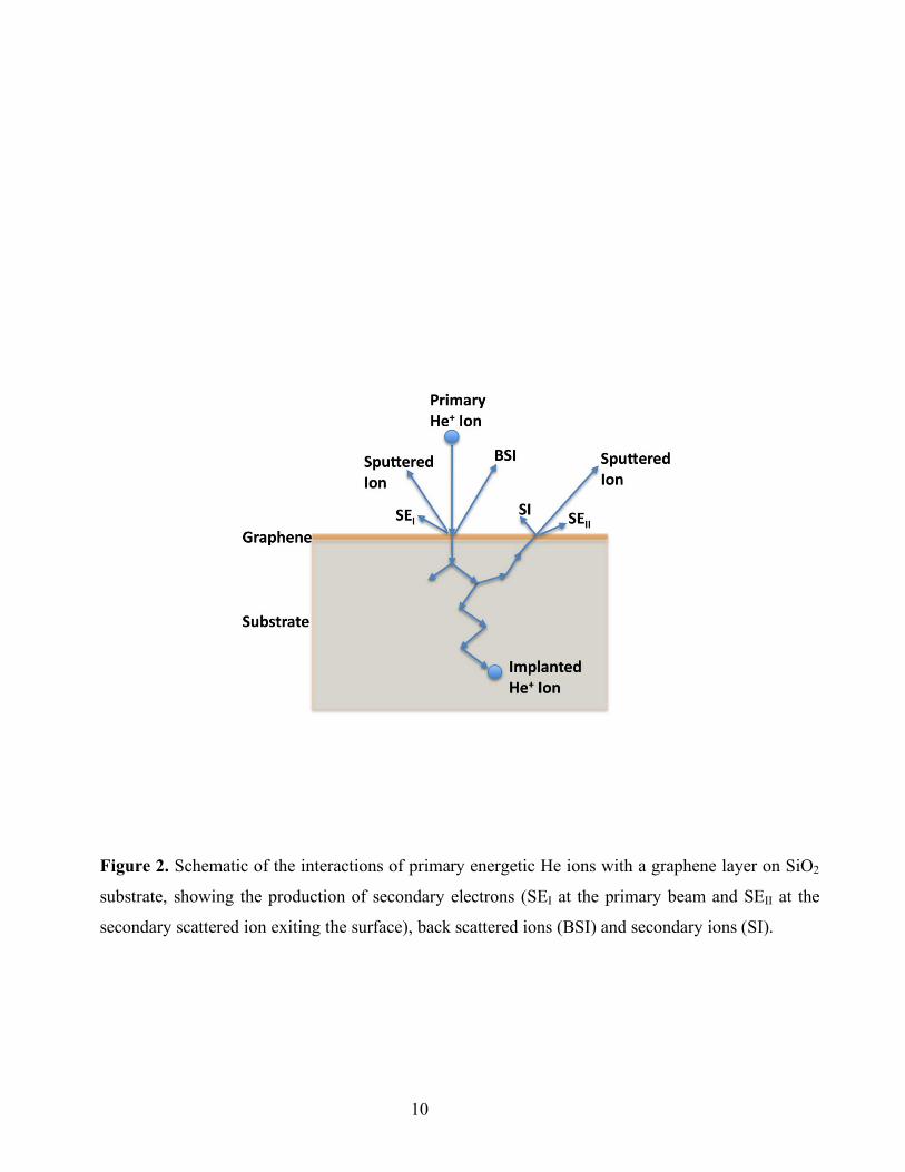
microscope as well as the minimum size of an etched line when used as a lithography tool. Figure
2. illustrates the interactions of primary energetic He ions with a graphene layer on SiO2 substrate
indicating the production of sputtered ions, secondary electrons (SEI at the primary beam and SEII
at the secondary scattered ion exiting the surface), back scattered ions (BSI) and secondary ions
(SI).
The size of the interaction region within the sample depends on the atomic mass and density of
the sample, and on the acceleration voltage. The interaction area at the sample surface is smaller
for HIL than for commercial electron-beam lithography or FIB systems by roughly a factor of
100.
Figure 3 shows a comparison of gallium and helium ion beam propagation into graphene on a
Si/SiO2 substrate, calculated using the TRIM software package [10][11]. For graphene on a
typical substrate of 285 nm SiO2 on silicon, the simulation shows the gallium atoms depositing
most of their kinetic energy in the upper most parts of the material (Fig. 3(a)). While this makes
gallium highly effective at bulk milling and etching, the resulting surface interaction area gives
feature sizes much larger than the actual beam diameter. TRIM calculations for helium ions on
an identical specimen, in contrast, show that 99.6% of the ions pass directly through the
graphene with no ion interaction at all. Instead, the majority of the ion energy is deposited deep
within the silicon substrate (Fig. 3(b)). These simulations suggest that the lighter mass and higher
speed of the helium ions results in smaller interaction volume with the surface layers and hence
better resolution and potential milling feature size. From the perspective of sputtering and
patterning, the result is a reduced proximity effect in the surface layer. The light ion mass results
in low energy transfer and hence a relatively lower sputtering yield compared to gallium.
Page 5
4
Figure 3(c) shows a simulation for a suspended layer of graphene over SiO2 and silicon substrate.
The thickness of the vacuum gap and the SiO2 add up to 285 nm, as would be the case in a
device fabricated from a typical substrate as in Fig. 3b. In this case, there is little to no
observable backscattering to the graphene layer. Experimental details of our suspended graphene
etching by helium ions have been described elsewhere [8] the inclusion of the modeling Fig. 3(c)
of suspended graphene is to show, for completeness the inherent differences of each etching
approach. In addition, the lack of interaction of backscattered ions with the graphene film should
make suspended devices particularly suitable for He ion etching.
Overall, these simulations suggest a factor of 10 reduction in feature size for helium ions
compared with gallium ions. Gallium ions also could leave ionic contamination in samples
which are problematic for graphene devices, Long-term trapping of helium ions is expected to be
much less severe. An important result from these simulations is the indication that the lack of
helium ion beam divergence in the vicinity of the surface of the sample down to a depth of about
100 nm should enable nanometer scale fine etching and cutting, with minimal surrounding area
damage. Following from the simulations [11], a model of proximity effect during ion
bombardment showing the differences between gallium and helium ion bombardment for milling
and etching (Insets in Fig. 3).
Experiment
Helium ion lithography and microscopy was carried out using a Zeiss ORION system, operated
at 30kV acceleration voltage with a beam current of 1 to 1.6 pA. While hydrocarbons have been
used previously to write patterns onto graphene [12], here such contamination is avoided: The
chamber is cleaned with air plasma overnight prior to sample patterning using an Evactron
plasma cleaner at 12 W with a least 10 on/off (15 minutes/45 minutes) cycles [13]. Beam control
for HIL used a modified Nabity Nanometer Pattern Generation System (NPGS). The Nabity
system allowed for dose computer-based pattern design, dosage variations, and alignment to
existing features, including sample edges [8]. Test writing was performed on 285 nm-thick SiO2
on a Si substrate. Initial dose exposures indicated a dose of 1.2 nC/cm as an optimal initial
setting for ion beam and dwell times in the pattern generation system. Atomic force microscope
(AFM) and helium ion microscopy images (Fig. 4(a,b)) shown sharp, well-defined patterned
etched in SiO2. AFM data was taken in tapping mode using a Digital Instruments Nanoscope III
Page 6
5
instrument. We used Veeco Tapping Mode Etched Silicon Probes (TESP) with a specified
nominal tip radius of curvature of 5-10 nm
Graphene flakes were then deposited onto the SiO2 by mechanical exfoliation, similar to the
method described in [3] with the modifications of the process as described in [8]. Next, mono-
and multi-layer graphene flakes were identified with an optical microscope.
Results and Discussion
In an initial experiment, a ion beam spot was focused on a SiO2 supported multi-layer graphene
flake, resulting in small holes in the material. Fig. 5 shows a helium ion micrograph of one such
hole with a diameter of ~ 15 nm. Variations of this dose were performed to ascertain the optimal
operation point for He ion etching. Figure 6(a) shows a helium ion micrograph of lines etched in
graphene sample, showing changes in the pattern with increasing beam dose from left to right at
a measured probe current of 1.6 pA. The dose was varied from 3 nC/cm to 15 nC/cm in 3 nC/cm
steps. Total patterning time varying between 3 and 6 seconds. The result indicates that a suitable
dose for etching a graphene sample with the present set-up is 10-15 nC/cm. A larger dose
variation performed with 20, 100 and 200 nC/cm is shown in Fig. 6(b). The scanning electron
microscope (SEM) image shows that all doses lead to a cut in the single-layer graphene.
However, the combination of SEM and AFM images further reveals that for very high doses the
underlying substrate can swell by at least 50 nm from the effect of ion knock-on damage to the
underlying silicon. The detailed AFM analysis for the single-layer graphene cut with the low
dose rate of 20 nC/cm for test lines resulted in a measured depth of 4 nm (Fig. 7).
NPGS software allows patterning of highly complex structures, as an example this is
demonstrated in Fig. 8 with a Harvard logo etched into a multi-layer graphene flake with line
widths of order 15 nm. The overall dimensions of the logo are about 4 µm x 5 µm.
Conclusions
We have shown that it is possible to precisely cut and pattern graphene using 30kV helium ions
using a modified helium ion microscope, configured with a commercial beam-patterning package
that allows control of beam dose, pattern configuration, and alignment to existing features. We
have demonstrated the technique by patterning single-layer and multilayer graphene samples,
Page 7
6
yielding sub-20nm feature sizes. We expect that this technique will facilitate graphene-based
electronic devices that take advantage of the unique physical properties of graphene.
Acknowledgements
MCL acknowledges the support of the Alexander von Humboldt foundation through a Feodor
Lynen Research Fellowship. Research also supported in part by the NRI INDEX program. The
authors thank S. Nakaharai for fruitful discussions regarding the process.
Page 8
7
References
[1] D.C. Bell, “Contrast Mechanisms and Image Formation in Helium Ion Microscopy”,
Microscopy and Microanalysis, 15 (2), pp 147-153, 2009.
[2] L. Scipioni, L.A. Stern, J. Notte, S. Sijranddij, B.J. Griffin, “Helium ion microscope”. Adv
Mater Proc 166, 27–30. 2008.
[3] K. S. Novoselov, A. K. Geim, S. V. Morozov, D. Jiang, Y. Zhang, S. V. Dubonos, I. V.
Grigorieva, and A. A. Firsov, “Electric Field Effect in Atomically Thin Carbon Films”,
Science, 306, pp. 666-669, October 2004.
[4] M.Y. Han, B. Özylimaz, Y. Zhang, P. Kim, “Energy band-gap engineering of graphene
nanoribbons“, Phys. Rev. Lett., Vol. 98, 2007.
[5] Z. Chen, Y.-M. Lin, M. J. Rooks, P. Avouris, “Graphene nano-ribbon electronics”, Physica
E, Vol. 40, Iss. 2, 2007.
[6] L.A. Ponomarenko, F. Schedin, M.I. Katsnelson, R. Yang, E.W. Hill, K.S. Novoselov,
A.K. Geim, “Chaotic Dirac Billard in Graphene Quantum Dots”, Science, Vol. 320, 2008.
[7] M.D. Fischbein, M. Drndi!, “Electron beam nanosculpting of suspended graphene sheets”,
Appl. Phys. Lett. 93, 113107, 2008.
[8] M.C. Lemme, D.C. Bell, J.R. Williams, L.A. Stern, B.W.H. Baugher, P. Jarillo-Herrero,
C.M. Marcus, “Etching of Graphene Devices with a Helium Ion Beam”, DOI
arXiv:0905.4409 May 2009.
[9] J.R. Williams, L. DiCarlo, C.M. Marcus, “Quantum Hall Effect in a Gate-Controlled p-n
Junction of Graphene”, Science, 317(5838):638-641, 2007.
[10] R.S. Averbeck, M. Ghaky, “A model for Surface Damage in Ion-Irradiated Solids”, Journal
of Applied Physics, 76 6, 3908 (1994).
[11] J. Zeigler, J. Biersack, U. Littmark, “The Stopping Range of Ions in Matter. New York
Pergamon Press (also at http://srim.org)
Page 9
8
[12] J.C. Meyer, C.O. Girit, M.F. Crommie, A. Zettl, “Hydrocarbon lithography on graphene
membranes”, Appl. Phys. Lett. 92, 123110, 2008.
[13] R Vane, “Immobilization and Removal of Hydrocarbon Contamination Using the Evactron
De-Contaminator”, Microscopy and Microanalysis, 12,(S02), pp. 1662-1663, 2006.
Page 10
9
Figure 1. Schematic of the Zeiss ORION helium ion microscope column, showing the ion source,
apertures, Everhart-Thornley secondary electron (E-T SE) detector and microchannel plate (MCP)
detector configuration. (Inset) Image of atomic trimer on a tungsten tip, where ionization occurs.
Page 11
10
Figure 2. Schematic of the interactions of primary energetic He ions with a graphene layer on SiO2
substrate, showing the production of secondary electrons (SEI at the primary beam and SEII at the
secondary scattered ion exiting the surface), back scattered ions (BSI) and secondary ions (SI).
Page 12
11
Figure 3. Simulations using TRIM software [10] comparing a) 30 kV Ga ions and b) 30kV He ions
for range and trajectory in graphene layers on SiO2 on silicon substrate. c) Range and trajectory of
30 kV He ions through a suspended graphene layer over vacuum, SiO2 and silicon substrate. (Insets)
Schematic comparison between Ga+ ion and He+ ion interaction with graphene samples from
molecular dynamics simulations [11].
Page 13
12
Figure 4. a) Test patterns written into a 285 nm SiO2 film on silicon substrate as measured with
AFM and b) Secondary electron image showing etching of boxes and line box patterns.
Page 14
13
Figure 5. Helium ion micrograph imaged with the secondary electrons of a hole etched into a multi
layer graphene flake (grey) on a SiO2 substrate (black).
Page 15
14
Figure 6. a) Helium ion micrographs of a dose variation test pattern in single-layer graphene, on
SiO2 substrate covering a range of linear doses from 3 nC/cm to 15 nC/cm in 3 nC/cm steps (left to
right). b) AFM image with corresponding SEM image of a pattern etched with 20, 100 and
200 nC/cm line dose variation (from left to right).
Page 16
15
Figure 7. a) AFM step profile analysis for the single-layer graphene cut in Fig. 6(b) with a dose rate
of 20 nC/cm resulting in a depth of 4 nm. b) AFM image used for the step profile. The profile was
taken along the upper part of the image, in the position and direction indicated by the arrow.
Page 17
16
Figure 8. Helium ion micrograph of a high resolution Harvard University logo etched by HIL into
multi-layer graphene flake.