• The Multiple Cycle Machine cannot be implemented simply as combinational logic. Why?
Because each instruction requires 3 -5 states (clock cycles) to complete.
• It will require a Finite State machine (FSM). A set of states. How many? Combinational logic for control signals. Combinational logic for next state inputs.
• It can be implemented with a PLA(s).
The Multicycle Datapath with Control Signals
Address
Read Data(Instr. or Data)
Memory
PC
Write Data
Read Addr 1
Read Addr 2
Write Addr
Register
File
Read Data 1
Read Data 2
ALU
Write Data
IRM
DR
AB
AL
Uo
ut
SignExtend
Shiftleft 2 ALU
control
Shiftleft 2
ALUOpControl
IRWriteMemtoReg
MemWriteMemRead
IorD
PCWrite
PCWriteCond
RegDstRegWrite
ALUSrcAALUSrcB
zero
PCSource
1
1
1
1
1
10
0
0
0
0
0
2
2
3
4
Instr[5-0]
Instr[25-0]
PC[31-28]
Instr[15-0]
Instr[3
1-2
6]
32
28
Multiple Clock Cycle Finite State Machine
Comparing Single and Multiple Clock Machines
Generating the Next State Equations
PLA Implementation of Multi Clock PLA
PLA Implementation of Multi Clock FSM
• An alternative to a FSM implementation.
• Most Computers today are at least partially implemented with Micro-program control
• The concept is to build a simpler internal computer (micro-computer) that implements the control sequences (micro-instructions) that are stored in a micro-computer memory (ROM)
• The advantage is ease of design, flexibility, and adaptability to “families of computers”.
• Particularly useful in CICS Machine Implementation.
Micro-Programmed Control
Control Unit Organization
Tasks of Control Unit:
• Microinstruction sequencing
• Microinstruction execution
The Control Memory contains sequences of microinstructions that provide the control signals to execute instruction cycles, e.g. Fetch, Indirect, Execute, and Interrupt.
Typical Microinstruction Formats
Microinstruction Encoding: Direct Encoding
Horizontal Micro-programming
• Wide control memory word
• High degree of parallel operations possible
• Little encoding of control information
• Relatively Fast
Microinstruction Encoding: Indirect Encoding
Vertical Micro-programming
• Word width can be much narrower
• Control signals encoded into function codes – need to be decoded
• More complex, more complicated to program, less flexibility
• More difficult to modify
• Slower
Next Address Decision ?
• Like a normal computer, we want to allow branches. Why?
• Target address depends upon “ALU flags” and control buffer register bits:
Get next instruction– Add 1 to control address register
Jump to machine instruction routine– Load control address register based on opcode in IR
Jump to other new routine based on jump microinstruction– Load address field of control buffer register into control
address register
Branch Control: Two Address Fields
Branch based upon:
• Instruction Opcode
• Address 1
• Address 2
Does require a wide microinstruction, but no address calculation is needed
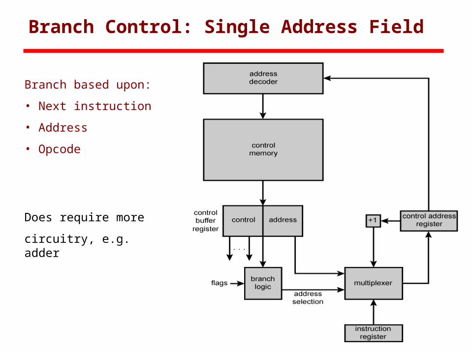
Branch Control: Single Address Field
Branch based upon:
• Next instruction
• Address
• Opcode
Does require more
circuitry, e.g. adder
Branch Control: Variable Format
One bit determines microinstruction format:
• Control signal format
• Branch format
Does require even more circuitry, and is slowest.
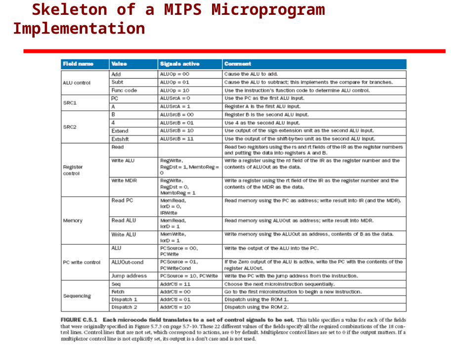
Skeleton of a MIPS Microprogram Implementation
Reflection on Microprogramming Control
• The advantage is ease of design, flexibility, and adaptability to “families of computers”.
• The disadvantage is speed.
• Particularly useful in CICS Machine implementation, since they have a lot of complex instructions and hence complex design requirements.
• One of the advantages of RISC machines is that they intrinsically simple and don’t need a lot of complex options and huge numbers of states to implement.
• In reality, our view of the MIPS RISC machine is distorted by the simplicity of the subset of the MIPS machine that we looked at.