20
Publication Number: BM45ADA Revision:1.1 Issue Date Feb. 16 ,2015 Pressure Sensor BM45ADA Bestow Mascot

Publication Number: BM45ADA Revision:1.1 Issue Date Feb. 16 ,2015
Pressure Sensor
BM45ADA
Bestow Mascot

Preliminary Datasheet BM45ADA
Publication Number: BM45ADA Revision:1.1 Issue Date Feb. 16 ,2015
General Description:
The BM45ADA is the pressure sensor which measures absolute pressures. It consists of a silicon
micro-machined sensing element chip and a signal conditioning ASIC. The ASIC is equipped with a 24-
bit resolution Σ-∆ ADC and outputs a highly precise pressure value as a digital value. The pressure
sensor element and the ASIC are mounted inside a system-in-package and wire-bonded to appropriate
contacts. The BM45ADA provides the digital output data with the format of I2C/SPI interface. It can
achieve ESD robustness, fast response time, high accuracy and linearity as well as long-term stability. All
measurement data is fully calibrated and temperature compensated. In addition, it allows for easy
system integration.
Features:
Piezo-resistive silicon micro-machined sensor
Absolute type pressure sensor
Pressure range : 260 to 1260 mBar
24-bit data output access I2C/SPI(3-wire/4-wire) interface
Supply voltage:1.7 to 3.6V
Embedded temperature compensation
Fast power up to first data ready : 15ms
Fast data update rate : 200Hz
QFN-8 pin package (2.5*2.5*1mm)
RoHS compliant and Halogen-free Package
Applications:
Altitude and Barometer for portable device
GPS application
Air Conditioning
Weather stations
Pneumatic control

Preliminary Datasheet BM45ADA
Publication Number: BM45ADA Revision:1.1 Issue Date Feb. 16 ,2015
Pin Configuration:
8
7
5
6
1
2
4
3
Top View
Pin No. Pin Name I/O Function description
1 GND P Connected to GND
2 CSB I SPI chip select; active low. When it is high, chip is in I2C mode.
Otherwise, chip is in SPI mode
3 SDA/SDI/SDI
O I/O I2C SDA/SPI SDI in 4-wire mode/SPI SDIO in 3-wire mode
4 SCL/SCK I I2C SCL/SPI SCK
5 I2C_AOPT/S
DO I/O I2C address bit 0 select in I2C mode/SDO in SPI mode
6 VDD_IO P Digital I/O power
7 GND P Connected to GND
8 GND P Positive supply voltage

Specification BM45ADA
Publication Number: BM45ADA Revision:1.1 Issue Date Feb. 16 ,2015
Block Diagram
Sensor bias
MUX
Temperature sensor
Pre‐Amplifier
ADC+Digitalfilter
UC coreIICSPI
Voltage Clock and Timing
p
Pressure sensor

Specification BM45ADA
Publication Number: BM45ADA Revision:1.1 Issue Date Feb. 16 ,2015
Maximum Ratings VDD ...................................................................................................................................... -0.3 V to +4.1 V
Voltage at Digital IO Pins............................................................................... ................ -0.3 V to VDD+0.3 V
Operating Temperature Range ............................................................................................. -40°C to +85°C
Storage Temperature Range................................................... ...................... ..................... -40°C to +125°C
Voltage (with respect to GND unless otherwise noted)
Electrical Characteristics
Symbol Parameter Test Conditions
Min. Typ. Max. Unit VDD Conditions
VDD Operating Voltage --- --- 1.7 3.0 3.6 V
IDD Operating Current 3.0V --- --- 1.6 --- mA
1.8V --- --- 0.7 --- mA
ISTB1 Standby Current 3.0V Sleep state at 25℃ --- 5 --- μA
TOP Full accuracy temperature
range --- --- -20 --- 85 ℃
PPRO Proof pressure --- --- --- --- 3000 mBar
POP Operating pressure range 3.0V --- 260 --- 1260 mBar
DR Data Resolution --- --- --- 24 --- bit
Psenty Pressure sensitivity --- --- --- 0.001 --- mBar/LSB
Pacc Accuracy pressure over
temperature 3.0V
T:25℃
P:900~1260mBar -3 --- +3 mBar
T:25℃
P:260~1260mBar -5 --- +5 mBar
T:0℃~50℃
P:260~1260mBar -10 --- +10 mBar
T:-20℃~85℃
P:260~1260mBar -17 --- +17 mBar
tADC AD conversion 3.0V T=25℃,FSYS(8MHz) --- 4.12 ---- mS
FSYS System Frequency 2.5~3.6V T:0℃~85℃ 7.96 8.00 8.04 MHz
Fc.I2C I2C clock frequency 3.0V --- --- 400 3400 KHz
Fscp SPI bus speed 3.0V except bit to bit
delay --- --- 10 MHz
ESD Human Body Mode --- MIL-STD-883E
Method 3015.7 -2 --- +2 kV

Specification BM45ADA
Publication Number: BM45ADA Revision:1.1 Issue Date Feb. 16 ,2015
I2C operation BM45ADA supports a bi-direction two wire bus and data transmission protocol to output data. A
processor sends data onto the bus is defined as transmitter, BM45ADA receives data is defined receiver.
The bus must be controlled by a master processor which generates the serial clock(SCL), controls the bus
access, and generates the START and STOP conditions, while the BM45ADA works as slave.
The following bus protocol has been defined:
Data transfer may be initiated only when the bus is not busy.
During data transfer, the data line must remain stable whenever the clock is HIGH level. Changes in
the data line while the clock line is HIGH will be interpreted as a START or STOP condition.
Following bus conditions have been defined
Bus not busy as condition(A)
Both data and clock lines remain HIGH.
Start data transfer as condition(B)
A HIGH to LOW transition of the SDA line while the clock (SCL) is HIGH determines as START
condition. Reading data must be begun by START condition.
Stop data transfer as condition(C)
A LOW to HIGH transition of the SDA line while the clock (SCL) is HIGH determines as STOP
condition.
Data valid as condition(D)
After a START condition, the data line is stable for the duration of the HIGH period of the clock signal.
The data on the line must be changed during the LOW period of the clock signal. There is one clock
pulse per bit of data. The number of valid data bytes transferred between the START and STOP
conditions.
Acknowledge signal
Each BM45ADA receiving, when addressed, is obliged to generate an acknowledge bit after the
reception of each byte. The processor must generate an extra clock pulse which is associated with
this acknowledge bit. The BM45ADA has to pull down the SDA line during the acknowledge clock
pulse. The way is the SDA line is stable LOW during the HIGH period of acknowledge related clock
pulse. A processor must signal an end of data to the slave by not generating an acknowledge bit on
the last byte.
BM45ADA I2C slave address
The seven bit is as slave address after START condition. The BM45ADA slave address is 1001101B
(7 bits). The eighth bit of control address is read or written bit that processor wants. The processor

Specification BM45ADA
Publication Number: BM45ADA Revision:1.1 Issue Date Feb. 16 ,2015
read data sequence refers as below:

Specification BM45ADA
Publication Number: BM45ADA Revision:1.1 Issue Date Feb. 16 ,2015
I2C Read/Write Format
Notation
S Start
P Stop
SAD+W Slave Address (1001 101) + Write bit ( 0 )
SAD+R Slave Address (1001 101) + Read bit ( 1 )
REG Register Address
DATA Data
A Master acknowledge
~A Master non-acknowledge
SAK Slave acknowledge
Master is writing one Byte to slave
Master S SAD+W REG DATA P
Slave SAK SAK SAK
Master is writing Multiple Bytes to slave
Master S SAD+W REG DATA DATA DATA P
Slave SAK SAK SAK SAK SAK
Master is reading one Byte from slave
Master S SAD+W REG S SAD+R ~A P
Slave SAK SAK SAK SAK DATA
Master is reading Multiple Bytes from slave
Master S SAD+W REG S SAD+R A A ~A P
Slave SAK SAK SAK SAK DATA DATA DATA
Read pressure data Format (I2C Interface)
Master S SAD+W
(100110
REG
(28H) S
SAD+R
(100110 A A ~A P
Slave SAK SAK SAK SAKP_DATA
<7:0>
P_DATA
<15:8>
P_DATA
<23:16>

Specification BM45ADA
Publication Number: BM45ADA Revision:1.1 Issue Date Feb. 16 ,2015
Read-out data format represents
Pressure Value Reading Data
<23:16> <15:8> <7:0>
260mBar 0x03 0xF7 0xA0
500mBar 0x07 0xA1 0x20
1000mBar 0x0F 0x42 0x40
1260mBar 0x13 0x39 0xE0
I2C Operation sequence
Step 1:
First, DRDY enable. Writing register address 21H as 0x2cH to BM45ADA access I2C interface.
Second, Control REG1 setting. Writing register address 20H as 0x98H to BM45ADA access I2C
interface.
Third, I2C Page Enable Register enable. Writing register address 3FH as 0x80H to BM45ADA
access I2C interface.
Step 2:
Fourth, I2C Page 0 setting. Writing register address 3EH as 0x00H to BM45ADA access I2C interface.
Fifth, Measurement Mode setting. Writing register address 46H as 0x0010H to BM45ADA access I2C
interface.
Step 3:
-1186Sixth, read-out digital pressure value after detecting rising edge of DRDY (Bit 6 Of STATUS
Register).
Reading 24-bit pressure data in register address 28H from BM45ADA access I2C interface.
Repeat step 3 to continue reading 24-bit pressure data from BM45ADA access I2C interface.
After pressure measurement completely, write register address 20H as 18H to BM45ADA going to
standby mode.

Specification BM45ADA
Publication Number: BM45ADA Revision:1.1 Issue Date Feb. 16 ,2015
System reading data diagram
*DRDY(Bit 6 Of STATUS Register ) switches to low form high while host read out the pressure data.
Symbol Parameter Min. Typ. Max. Unit
tpd Power on
delay time 11 - - ms
td1 Delay time for
1st data ready 4 - - ms
Td2 Data update
rate time - 5 - ms
I2C interface timing
Symbol Parameter Fast mode High speed mode
UnitMin Max Min Min
fSCL SCL clock frequency --- 400 --- 3400 Hz
tL(SCL) SCL clock low time 1.3 --- 0.16 --- us
tH(SCL) SCL clock high time 0.6 --- 0.06 --- us
tr(SCL) / tr(SDA) SCL and SDA rise time --- 300 --- 10 ns
tf(SCL) / tf(SDA) SCL and SDA fall time --- 300 --- 10 ns
ts(SDA) SDA setup time 100 --- 10 --- ns
th(SDA) SDA hold time 0 --- 0 --- ns
ts(STA) Setup time for START condition 0.6 --- 0.16 --- us

Specification BM45ADA
Publication Number: BM45ADA Revision:1.1 Issue Date Feb. 16 ,2015
Command table description Register Address Bit Command Description
CTRL_1 0x20 7:0 Write 0x98 Start measurement, ODR: 200Hz
Write 0x18 System Stand by
CTRL_2 0x21 CTRL_2Write 0x24 Disable DRDY function
Write 0x2c Enable DRDY (Active High).
CTRL_3 0x46 15:0 Write
0x0010 Measurement Mode Enable
Pressure Output
Data L 0x28 7:0 Read Pressure Output Low Byte Data
Pressure Output
Data M 0x29 7:0 Read Pressure Output Medium Byte Data
Pressure Output
Data H 0x2A 7:0 Read Pressure Output High Byte Data
I2C Page Register 0x3E 7:0 Write 0x00
Changed to I2C Page 0
*The I2C page is changeable while
I2C Page Enable Register = 0x80.
I2C Page Enable
Register 0x3F 7:0 Write 0x80
After enable, user can change I2C
Page number.
CTRL_1
CTRL_REG1(0x20)
Bit Description Attr Default Attr Default
7
PC1: Stand-by or Active mode
0 = Stand-by –mode (default after POR)
1 = Active-mode
R/W 0
6:5 Reserved R/W 0
4:3
ODR12: Pressure measurement Output Data Rates
11 = ODR3 =200 Hz
10 = ODR2 = 50 Hz
00 = ODR1 =5 Hz (default after POR)
01 = ODR0 = 1 Hz
R/W 0
2 Reserved R 0
1
FS1: Functional State
0 = Normal -Mode
1 = Normal –Mode Disable (default after POR)
R/W 1
0 Reserved R 0

Specification BM45ADA
Publication Number: BM45ADA Revision:1.1 Issue Date Feb. 16 ,2015
STATUS Register STAT(0x27)
Bit Description Attr Default Attr Default
7 Reserved R 0
6
DRDY:
Data ready status
0 = data not ready, 1 = data ready valid
- data ready signal is following stream data ODR selection
- Data ready physical signal disabled/enabled in register
/CNTL2, bit DREN
R 0
5 Reserved R 0
4 Reserved R 0
3 Reserved R 0
2 Reserved R 0
1 Reserved R 0
0 Reserved R 0
I2C Page Register
I2C Page Register (0x3E)
Bit Description Attr Default Attr Default
7:4 I2C PAGE: I2C page number
*This 4 bits are changeable while I2C_PAGE_CHANGE_EN= 1 R/W 0xF
3
SPI_BANK_BIT:
SPI_PAGE/BANK = { I2C_PAGE, SPI_BANK_BIT}
*This bit is changeable while I2C_PAGE_CHANGE_EN = 1
R/W 0x0
2:0 Reserved R 0
I2C_PAGE_EN Register
I2C_Page_EN Register 1 (0x3F)
Bit Description Attr Default Attr Default
7
I2C(SPI)_PAGE_CHANGE_EN
When this bit is set, user can change the I2C_PAGE. Once
user writes the I2C_PAGE/SPI_BANK_BIT/SPI_3_WIRE, this bit will be
cleared.
R/W 0
6:0 Reserved 0 0
Specification BM45ADA
Publication Number: BM45ADA Revision:1.1 Issue Date Feb. 16 ,2015
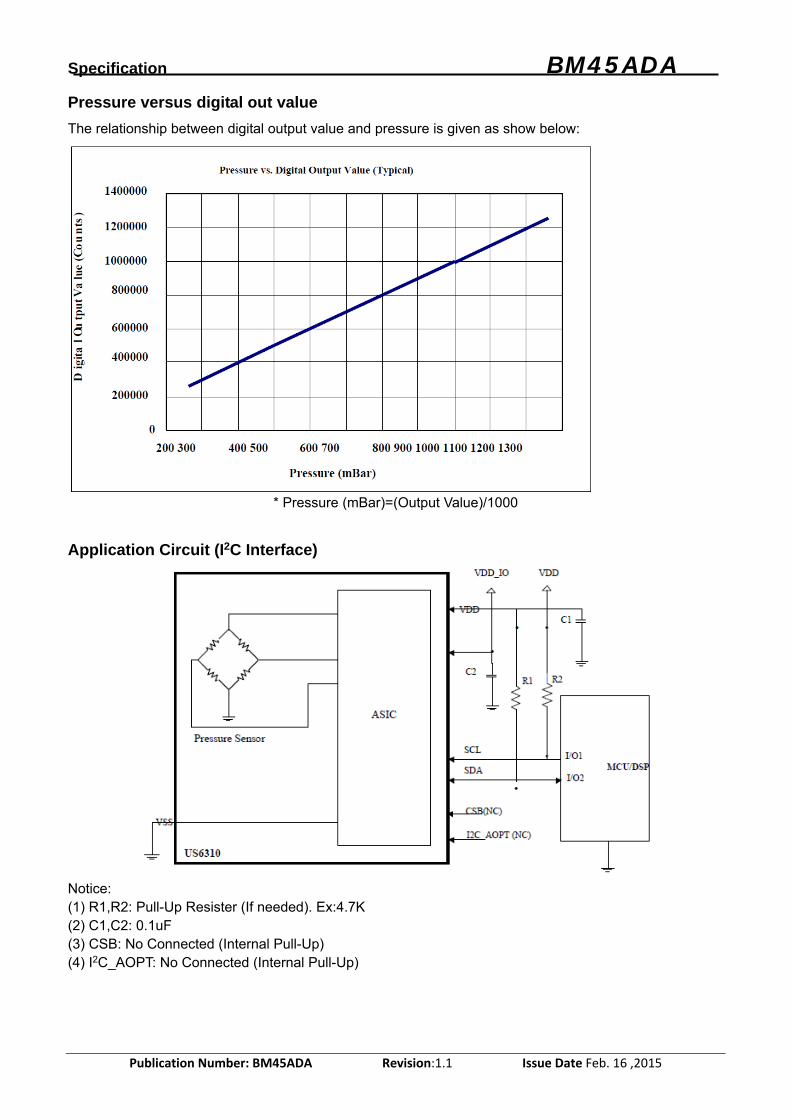
Pressure versus digital out value
The relationship between digital output value and pressure is given as show below:
* Pressure (mBar)=(Output Value)/1000
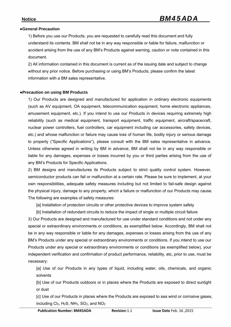
Application Circuit (I2C Interface)
Notice: (1) R1,R2: Pull-Up Resister (If needed). Ex:4.7K (2) C1,C2: 0.1uF (3) CSB: No Connected (Internal Pull-Up) (4) I2C_AOPT: No Connected (Internal Pull-Up)

Ordering Information BM45ADA
Publication Number: BM45ADA Revision:1.1 Issue Date Feb. 16 ,2015
BM 45 A D A Q R G
Series Name
Bestow Mascot Technology Ltd.
Company Prefix
45: Pressure Sensor
Measure Type
A‐Absolute Type
Package Type
Q‐QFN
Pack Type
R‐Tape&Reel
Plating Technology
R‐RoHS compliant G‐Green (Halogen‐free)
Version
Output Data Type
D‐Digital Data

Package Information BM45ADA
Publication Number: BM45ADA Revision:1.1 Issue Date Feb. 16 ,2015
Package Information (Unit:mm)
QFN Package Outline Dimension
Notice BM45ADA
Publication Number: BM45ADA Revision:1.1 Issue Date Feb. 16 ,2015
●General Precaution
1) Before you use our Products, you are requested to carefully read this document and fully
understand its contents. BM shall not be in any way responsible or liable for failure, malfunction or
accident arising from the use of any BM’s Products against warning, caution or note contained in this
document.
2) All information contained in this document is current as of the issuing date and subject to change
without any prior notice. Before purchasing or using BM’s Products, please confirm the latest
information with a BM sales representative.
●Precaution on using BM Products
1) Our Products are designed and manufactured for application in ordinary electronic equipments
(such as AV equipment, OA equipment, telecommunication equipment, home electronic appliances,
amusement equipment, etc.). If you intend to use our Products in devices requiring extremely high
reliability (such as medical equipment, transport equipment, traffic equipment, aircraft/spacecraft,
nuclear power controllers, fuel controllers, car equipment including car accessories, safety devices,
etc.) and whose malfunction or failure may cause loss of human life, bodily injury or serious damage
to property (“Specific Applications”), please consult with the BM sales representative in advance.
Unless otherwise agreed in writing by BM in advance, BM shall not be in any way responsible or
liable for any damages, expenses or losses incurred by you or third parties arising from the use of
any BM’s Products for Specific Applications.
2) BM designs and manufactures its Products subject to strict quality control system. However,
semiconductor products can fail or malfunction at a certain rate. Please be sure to implement, at your
own responsibilities, adequate safety measures including but not limited to fail-safe design against
the physical injury, damage to any property, which a failure or malfunction of our Products may cause.
The following are examples of safety measures:
[a] Installation of protection circuits or other protective devices to improve system safety
[b] Installation of redundant circuits to reduce the impact of single or multiple circuit failure
3) Our Products are designed and manufactured for use under standard conditions and not under any
special or extraordinary environments or conditions, as exemplified below. Accordingly, BM shall not
be in any way responsible or liable for any damages, expenses or losses arising from the use of any
BM’s Products under any special or extraordinary environments or conditions. If you intend to use our
Products under any special or extraordinary environments or conditions (as exemplified below), your
independent verification and confirmation of product performance, reliability, etc, prior to use, must be
necessary:
[a] Use of our Products in any types of liquid, including water, oils, chemicals, and organic
solvents
[b] Use of our Products outdoors or in places where the Products are exposed to direct sunlight
or dust
[c] Use of our Products in places where the Products are exposed to sea wind or corrosive gases,
including Cl2, H2S, NH3, SO2, and NO2

Notice BM45ADA
Publication Number: BM45ADA Revision:1.1 Issue Date Feb. 16 ,2015
[d] Use of our Products in places where the Products are exposed to static electricity or
electromagnetic waves
[e] Use of our Products in proximity to heat-producing components, plastic cords, or other
flammable items
[f] Sealing or coating our Products with resin or other coating materials
[g] Use of our Products without cleaning residue of flux (even if you use no-clean type fluxes,
cleaning residue of flux is recommended); or Washing our Products by using water or water-
soluble cleaning agents for cleaning residue after soldering
[h] Use of the Products in places subject to dew condensation
4) The Products are not subject to radiation-proof design.
5) Please verify and confirm characteristics of the final or mounted products in using the Products.
6) In particular, if a transient load (a large amount of load applied in a short period of time, such as
pulse) is applied, confirmation of performance characteristics after on-board mounting is strongly
recommended. Avoid applying power exceeding normal rated power; exceeding the power rating
under steady-state loading condition may negatively affect product performance and reliability.
7) De-rate Power Dissipation (Pd) depending on Ambient temperature (Ta). When used in sealed
area, confirm the actual ambient temperature.
8) Confirm that operation temperature is within the specified range described in the product
specification.
9) BM shall not be in any way responsible or liable for failure induced under deviant condition from
what is defined in this document.
●Precaution for Mounting / Circuit board design
1) When a highly active halogen us (chlorine, bromine, etc.) flux is used, the residue of flux may
negatively affect product performance and reliability.
2) In principle, the reflow soldering method must be used; if flow soldering method is preferred,
please consult with the BM representative in advance. For details, please refer to BM Mounting
specification
●Precautions Regarding Application Examples and External Circuits
1) If change is made to the constant of an external circuit, please allow a sufficient margin
considering variations of the characteristics of the Products and external components, including
transient characteristics, as well as static characteristics.
2) You agree that application notes, reference designs, and associated data and information
contained in this document are presented only as guidance for Products use. Therefore, in case you
use such information, you are solely responsible for it and you must exercise your own independent
verification and judgment in the use of such information contained in this document. BM shall not be
in any way responsible or liable for any damages, expenses or losses incurred by you or third parties
arising from the use of such information.

Notice BM45ADA
Publication Number: BM45ADA Revision:1.1 Issue Date Feb. 16 ,2015
●Precaution for Electrostatic
This Product is electrostatic sensitive product, which may be damaged due to electrostatic discharge.
Please take proper caution in your manufacturing process and storage so that voltage exceeding the
Products maximum rating will not be applied to Products. Please take special care under dry
condition (e.g. Grounding of human body / equipment / solder iron, isolation from charged objects,
setting of Ionizer, friction prevention and temperature / humidity control).
●Precaution for Storage / Transportation
1) Product performance and soldered connections may deteriorate if the Products are stored in the
places where:
[a] the Products are exposed to sea winds or corrosive gases, including Cl2, H2S, NH3, SO2, and
NO2
[b] the temperature or humidity exceeds those recommended by BM
[c] the Products are exposed to direct sunshine or condensation
[d] the Products are exposed to high Electrostatic
2) Even under BM recommended storage condition, solder ability of products out of recommended
storage time period may be degraded. It is strongly recommended to confirm solder ability before
using Products of which storage time is exceeding the recommended storage time period.
3) Store / transport cartons in the correct direction, which is indicated on a carton with a symbol.
Otherwise bent leads may occur due to excessive stress applied when dropping of a carton.
4) Use Products within the specified time after opening a humidity barrier bag. Baking is required
before using Products of which storage time is exceeding the recommended storage time period.
●Precaution for Product Label
QR code printed on BM Products label is for BM’s internal use only.
●Precaution for Disposition
When disposing Products please dispose them properly using an authorized industry waste company.
●Precaution for Foreign Exchange and Foreign Trade act
Since our Products might fall under controlled goods prescribed by the applicable foreign exchange
and foreign trade act, please consult with BM representative in case of export.
●Precaution Regarding Intellectual Property Rights
1) All information and data including but not limited to application example contained in this document
is for reference only. BM does not warrant that foregoing information or data will not infringe any
intellectual property rights or any other rights of any third party regarding such information or data.
BM shall not be in any way responsible or liable for infringement of any intellectual property rights or
other damages arising from use of such information or data.
2) No license, expressly or implied, is granted hereby under any intellectual property rights or other

Notice BM45ADA
Publication Number: BM45ADA Revision:1.1 Issue Date Feb. 16 ,2015
rights of BM or any third parties with respect to the information contained in this document.
●Other Precaution
1) The information contained in this document is provided on an “as is” basis and BM does not
warrant that all information contained in this document is accurate and/or error-free. BM shall not
be in any way responsible or liable for any damages, expenses or losses incurred by you or third
parties resulting from inaccuracy or errors of or concerning such information.
2) This document may not be reprinted or reproduced, in whole or in part, without prior written
consent of BM.
3) The Products may not be disassembled, converted, modified, reproduced or otherwise changed
without prior written consent of BM.
4) In no event shall you use in any way whatsoever the Products and the related technical
information contained in the Products or this document for any military purposes, including but not
limited to, the development of mass-destruction weapons.
5) The proper names of companies or products described in this document are trademarks or
registered trademarks of BM, its affiliated companies or third parties.

Version Information BM45ADA
Publication Number: BM45ADA Revision:1.1 Issue Date Feb. 16 ,2015
Version Publication date Pages Revise Description
1.0 Jan.2015 19 Initial Document Release
1.1 Feb.2015 13 Update ordering information


