of the microstrip line and the misalignment of the via arrays in
the substrate ought to be examined. Simulation results indicate
that the performance of the proposed transition can tolerate fab-
rication and assembly errors to a reasonable amount. For a
microstrip line fabricated on a substrate thinner than the gap,
solder on the via arrays is required to prevent sideward leakage
through the additional air space above the substrate within the
gap. Thicker substrates are not discussed here because they usu-
ally are not considered for high-frequency applications. The new
connector is also proved to be suitable for the transitions
between various coaxial cables/connectors and different planar
transmission lines, such as K-to-microstrip, semi-rigid cable-to-
microstrip, and SMA-to-CPW transitions as well.
5. CONCLUSION
A new SMA connector designed for coaxial-to-microstrip transi-
tions is presented. The connector is combined with two via
arrays embedded in the substrate of the microstrip line to facili-
tate the transformation of the field distributions of the two trans-
mission lines. Hence, the high-frequency performance of the
transition is improved significantly. The design offers reasonable
amount of tolerances for the fabrication errors of the new con-
nector and the via arrays. It can apply to the transitions between
other cables/connectors and planar transmission lines as well.
These features make the proposed design most suitable for high-
frequency applications.
REFERENCES
1. R.L. Eisenhart, A better microstrip connector, In: Proc IEEE-MTT
Symp, 1978, pp. 318–320.
2. J. Chenkin, dc to 40 GHz coaxial-to-microstrip transition for 100-
l-thick GaAs substrates, IEEE Trans Microwave Theory Tech 37
(1989), 1147–1150.
3. J.-C. Cheng, E.S. Li, W.-F. Chou, and K.-L. Huang, Improving the
high-frequency performance of coaxial-to-microstrip transitions,
IEEE Trans Microwave Theory Tech 59 (2011), 1468–1477.
4. HFSS (High frequency structure synthesizer) ver. 11, Ansoft Cor-
poration, Pittsburgh, PA, 2007.
5. F. Shigeki, Waveguide line, (in Japanese) Japan Patent 06-053 711,
1994.
6. R.A. Soares, P. Gouzien, P. Leguad, and G. Follot, A unified mathe-
matical ap- proach to two-port calibration techniques and some appli-
cations, IEEE Trans. Microwave Theory Tech 37 (1989), 1669–1674.
VC 2012 Wiley Periodicals, Inc.
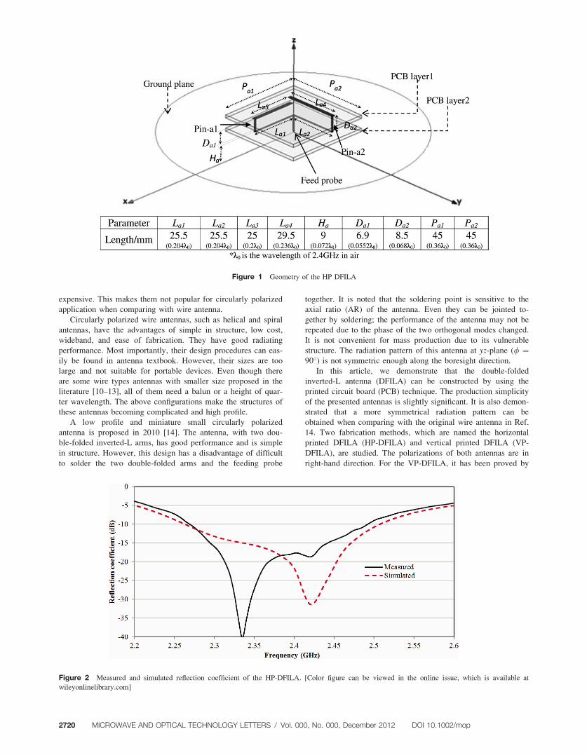
PRINTED CIRCULARLY POLARIZED WIREANTENNAS WITH DC GROUNDED STUB
Song Wang,1 Ka Ming Mak,2 Hau Wah Lai,2,3 Kwok Kan So,2,3
Quan Xue,2,3 and Guisheng Liao1
1National Laboratory of Radar Signal Processing, Xidian University,Xi’an 710071, China2 State Key Laboratory of Millimeter waves (HK), City University ofHong Kong SAR, China3 Shenzhen Research Institute, City University of Hong Kong,Shenzhen, China; Corresponding author: [email protected]
Received 13 March 2012
ABSTRACT: Two new printed circuit board types double-folded
inverted-L antennas (DFILAs), which are the horizontal printed DFILAand the vertical printed DFILA, have been proposed. By takingadvantage of the printed circuit technologies, the manufacturing
processes of the DFILAs can be simplified. The proposed antennas arelow profile, lightweight, and simple in structure. Both antennas perform
right-hand circular polarization with center frequency of 2.4 GHz. Bothantennas have impedance bandwidths of over 7% (S11<�10dB) andaxial ratios of 2.5% (< 3dB). The gains of the two antennas are higher
than 6.4 dBi. One of the designs has a simple feeding network with aDC grounded stub, which can improve the impedance matching andprovide static discharges for the DFILA. VC 2012 Wiley Periodicals, Inc.
Microwave Opt Technol Lett 54:2719–2725, 2012; View this article
online at wileyonlinelibrary.com. DOI 10.1002/mop.27181
Key words: wire antenna; printed circuit board; circular polarization
1. INTRODUCTION
Circular polarization has the advantages of reducing multipath
effect, inclement weather, and suitable for line-of-sight between
a transmitter and receiver. Therefore, it is suitable for satellite
communication, global positioning system, radar tracking, and
RFID. For wireless communication, the use of a circularly polar-
ized antenna with the same corresponding hand is necessary to
optimize the quality. Wire antennas, such as helix [1–3] and spi-
ral [4, 5], are some classical examples of circularly polarized
antenna. Patch [6, 7] and dielectric resonator antenna [8, 9] can
be utilized to produce circularly polarized radiation; however,
they, respectively, have the weakness of narrow band and
Figure 7 Phase and group delay responses of the back-to-back con-
nection of two proposed coaxial-to-microstrip transitions
Figure 8 Frequency responses of a single proposed coaxial-to-micro-
strip transition
DOI 10.1002/mop MICROWAVE AND OPTICAL TECHNOLOGY LETTERS / Vol. 000, No. 000, December 2012 2719
expensive. This makes them not popular for circularly polarized
application when comparing with wire antenna.
Circularly polarized wire antennas, such as helical and spiral
antennas, have the advantages of simple in structure, low cost,
wideband, and ease of fabrication. They have good radiating
performance. Most importantly, their design procedures can eas-
ily be found in antenna textbook. However, their sizes are too
large and not suitable for portable devices. Even though there
are some wire types antennas with smaller size proposed in the
literature [10–13], all of them need a balun or a height of quar-
ter wavelength. The above configurations make the structures of
these antennas becoming complicated and high profile.
A low profile and miniature small circularly polarized
antenna is proposed in 2010 [14]. The antenna, with two dou-
ble-folded inverted-L arms, has good performance and is simple
in structure. However, this design has a disadvantage of difficult
to solder the two double-folded arms and the feeding probe
together. It is noted that the soldering point is sensitive to the
axial ratio (AR) of the antenna. Even they can be jointed to-
gether by soldering; the performance of the antenna may not be
repeated due to the phase of the two orthogonal modes changed.
It is not convenient for mass production due to its vulnerable
structure. The radiation pattern of this antenna at yz-plane (/ ¼90�) is not symmetric enough along the boresight direction.
In this article, we demonstrate that the double-folded
inverted-L antenna (DFILA) can be constructed by using the
printed circuit board (PCB) technique. The production simplicity
of the presented antennas is slightly significant. It is also demon-
strated that a more symmetrical radiation pattern can be
obtained when comparing with the original wire antenna in Ref.
14. Two fabrication methods, which are named the horizontal
printed DFILA (HP-DFILA) and vertical printed DFILA (VP-
DFILA), are studied. The polarizations of both antennas are in
right-hand direction. For the VP-DFILA, it has been proved by
Figure 1 Geometry of the HP DFILA
Figure 2 Measured and simulated reflection coefficient of the HP-DFILA. [Color figure can be viewed in the online issue, which is available at
wileyonlinelibrary.com]
2720 MICROWAVE AND OPTICAL TECHNOLOGY LETTERS / Vol. 000, No. 000, December 2012 DOI 10.1002/mop
both simulation and experiment that by introducing a simple
matching network, the impedance matching of the antenna can
be improved effectively.
2. HORIZONTAL PRINTED DFILA
2.1. Antenna GeometryThe geometry of the HP-DFILA is shown in Figure 1. It shows
that the antenna has two square PCB layers, two pins, a feeding
probe, and a ground plane. The material of the PCB is FR4 (er
¼ 4.4) and its thickness is 1.6 mm. There are two strip lines,
which have widths of 1.5 mm, printed on the top and bottom
surface of PCB layer 1. They, respectively, have length La4 ¼29.5 mm (0.236 k0) and La3 ¼ 25 mm (0.2 k0), and they are
located along y and x direction. There is a V-shape strip line
with arm lengths La1 ¼ 25.5 mm (0.204 k0) and La2 ¼ 25.5 mm
(0.204 k0) and width 1mm (0.008 k0) etching orthogonally on
the bottom side of PCB layer 2. The strip lines on PCB layer 1
are connected to this V-shape strip line on PCB layer 2 by sol-
dering the conducting pin-a1 and pin-a2. Both conducting pins
have diameter of 1 mm (0.008 k0) and their lengths Da1 and Da2
are 6.9 mm (0.0552 k0) and 8.5 mm (0.068 k0), respectively.
The lengths of the two square PCBs are the same and equal to
45 mm (0.36 k0). These PCBs are supported by plastic spacers
and fixed by plastic screws. For the excitation, there is a feeding
probe linked between a SMA connector and the intersection
point between La1 and La2 of the V shape strip line. The length
of the feeding probe is Ha and is equal to 9 mm (0.072 k0). It
can be seen in Figure 1 that the feeding position is the center of
the circular ground plane. The diameter of the circular ground
plane is 130 mm (1.04 k0). The total lengths of the double-
folded inverted-L lines at the x direction and y direction are,
respectively, 0.53 k0 (¼ Ha þ La1 þ Da1 þ La3) and 0.58 k0
(¼ Ha þ La2 þ Da2 þ La4).
2.2. Simulated and Experimental ResultsThe performances of the two antennas (HP-DFILA and VP-
DFILA) were modeled and validated by a commercial finite-ele-
ment analysis software HFSS. The measured impedance match-
ing is obtained by a VNA E5071C; while the gain and radiation
pattern of the antennas are measured by the Satimo STARLAB
near-field measurement system.
Figure 2 shows the simulated and measured reflection coeffi-
cient of the HP-DFILA. Results show that the simulated fre-
quency range for reflection coefficient below �10dB is between
2.26 and 2.52 GHz, which is 11%; while the corresponding
range by measurement is between 2.27 and 2.49 GHz and has a
bandwidth of 9.24%. In Figure 3, it is shown that the simulated
and measured AR bandwidths (less than 3dB) are 3.74%
(�2.36–2.45 GHz) and 2.7% (�2.4–2.465 GHz). The frequency
with minimum AR is 2.4 GHz by simulation and is 2.43 GHz
by measurement. The percentage error between simulation and
experiment is 1.25%. Figure 3 also shows the simulated and
measured gains of the antenna in the boresight direction. It is
noted that the gain is 6.8 dBi at 2.43 GHz. The simulated gain
is around 0.4 dB less than the measured gain. The difference
between theoretical and experiment is only 5%.
In Figure 4(a), the simulated radiation pattern of the antenna
at 2.4 GHz is plotted. It can be seen that the antenna is right
hand circularly polarized as the right-hand circularly polarized
radiation is much stronger than the left-hand circularly polarized
radiation. The simulated 3 dB beamwidth is about 74.5� in / ¼0� plane (xz-plane) and 69� in / ¼ 90� plane (yz-plane). In Fig-
ure 4(b), the measured radiation pattern at 2.43 GHz of the HP-
DFILA is shown. The radiation pattern at this frequency is
shown because minimum AR is obtained by measurement. The
measured 3 dB beamwidth is about 80� in / ¼ 0� plane and
74� in / ¼ 90� plane. The LHCP level is 14 dB lower than the
RHCP level and the back lobe level of the antenna is below
16 dB across the operating bandwidth. The results show that the
Figure 3 Measured and simulated gain and AR of the HP-DFILA.
[Color figure can be viewed in the online issue, which is available at
wileyonlinelibrary.com]
Figure 4 Radiation pattern of the HP-DFILA (a) simulated at 2.4 GHz and (b) measured at 2.43 GHz
DOI 10.1002/mop MICROWAVE AND OPTICAL TECHNOLOGY LETTERS / Vol. 000, No. 000, December 2012 2721
3-dB beamwidth of the antenna is stable in both 0 and 90�
planes across the operating bandwidth.
3. VERTICAL PRINTED DFILA
3.1. Antenna GeometryThe geometry of the VP-DFILA is shown in Figure 5. The
antenna has three PCBs, a feeding probe, and a ground plane.
As shown in Figure 5, the material of the two vertical PCBs is
FR4 with thicknesses of 1.6 mm. The two PCBs, which are
PCB-X and PCB-Y, are intersected together orthogonally and
form a ‘‘X’’ shape structure. Both FR4 PCBs have a double-
folded inverted-L strip line etching on one surface. A bended
portion is designed at Lb3. It is bended downward with e ¼ 2
mm to prevent the two double-folded inverted-L lines overlap-
ping together at point E; while the two metal lines are soldered
together at point ‘‘C’’. The widths of the lines are 1 mm. The
total length of the double-folded inverted-L lines at x and ydirection are 0.48 and 0.52 k0, respectively. Their detail lengths
are clearly shown in Figures 5(c) and 5(d). The size of the VP-
DFILA is the same as the HP-DFILA in Section 2
Even though the AR bandwidth of the VP-DFILA has been
optimized, its impedance cannot be matched to 50 X at 2.4
GHz. It is because when the two double-folded inverted-L lines
are located vertically, the resistive impedance reduced and the
reactive impedance increased. The impedance matching of the
antenna cannot be optimized to 50 X by tuning the parameters
of the two double-folded inverted-L lines on PCB-X and PCB-
Y. To optimize the impedance of the antenna, an extra matching
network printed on MN-PCB is used. The thickness of the MN-
PCB is 1 mm and its dielectric constant is 2.65. For the resistive
impedance, a microstrip line with quarter wavelength is used to
increase the resistive impedance. The width and length of the
quarter wavelength are, respectively, 3.5 mm (0.046 kg) and 21
mm (0.27 kg). While to reduce the reactive impedance, a short
circuit stub is introduced. The width and length of the short cir-
cuit stub are, respectively, 2 mm (0.026 kg) and 7.5 mm (0.098
kg). The microstrip line with quarter wavelength transform has
one end connected to the DFILA at point ‘‘J’’ and one end con-
nected to a SMA connector by a feeding probe.
3.2. Simulated and Experimental ResultsFigure 6 gives the simulated as well as the measured reflection
coefficients of the VP-DFILA. It can be seen that the measured
impedance bandwidth (reflection coefficient < �10dB) is 7.6%,
which is from 2.345 to 2.535 GHz; while the corresponding
simulated result is 8.8% and the range is between 2.34 and
Figure 5 Geometry of the VP DFILA. [Color figure can be viewed in the online issue, which is available at wileyonlinelibrary.com]
Figure 6 Measured and simulated reflection coefficient of the VP-
DFILA. [Color figure can be viewed in the online issue, which is avail-
able at wileyonlinelibrary.com]
2722 MICROWAVE AND OPTICAL TECHNOLOGY LETTERS / Vol. 000, No. 000, December 2012 DOI 10.1002/mop
2.555 GHz. Both of them can cover 2.4 GHz. Figure 8 shows
the 3-dB AR bandwidths of the VP-DFILA by measurement
and HFSS simulation. It can be seen that the measured and
simulated AR bandwidth is 2.5 and 2.9%. The minimum AR is
achieved at 2.4 GHz by simulation and at 2.415 by experiment.
It is demonstrated in Figure 7 that the VP-DFILA has meas-
ured gain of 6.5 dBi and simulated gain of 6 dBi at the þzdirection.
The simulated and measured radiation patterns of the VP-
DFILA are illustrated in Figure 8. For a fair comparison, the
radiation patterns with minimum AR are studied. The simulated
radiation pattern at 2.4 GHz and measured radiation pattern at
2.415 GHz are plotted. The difference between simulation and
experiment in percentage is 0.625%, which is very low. The
data show that the polarization of this antenna is right hand,
which is same as the HP-DFILA in Section 2.
From the simulated radiation in Figure 8(a), it shows that the
antenna has simulated half power beamwidths of 81.5� at / ¼0� plane and 77.5� at / ¼ 90� plane. The measured half power
beamwidths at / ¼ 0� and 90� plane are both 74�, which is
shown in Figure 8(b). The measured LHCP level is 16 dB lower
than the RHCP level and the back lobe level of the antenna is
below 18 dB across the operating bandwidth. Results show that
the 3-dB beamwidth of the antenna is stable in both 0� and 90�
planes across the operating bandwidth.
Figure 7 Measured and simulated gain and AR of the VP-DFILA.
[Color figure can be viewed in the online issue, which is available at
wileyonlinelibrary.com]
Figure 8 Radiation pattern of the VP-DFILA (a) simulated at 2.4 GHz (b) measured at 2.415 GHz
Figure 9 Prototype of the HP-DFILA. [Color figure can be viewed in the online issue, which is available at wileyonlinelibrary.com]
DOI 10.1002/mop MICROWAVE AND OPTICAL TECHNOLOGY LETTERS / Vol. 000, No. 000, December 2012 2723
4. DISCUSSION
By using PCB technique, two simple and practical circularly
polarized antennas are fabricated. They are the HP-DFILA and
VP-DFILA. Their prototypes are shown in Figures 9 and 10,
respectively. It is commonly known that fabrication by PCB is
very suitable for mass production as the manufacturing process
becoming simpler. By using PCB to fabricate antenna, the per-
formances can also be repeatable.
Other than having several advantages in manufacturing, the
results in this article also show that the performance of the
DFILA [14] can be improved, which is mainly in the radiation
pattern. Figure 5 shows the radiation pattern of the HP-DFILA.
It is noted that the radiation pattern is very symmetric at / ¼ 0�
plane; while there is a two or three degree rotation toward the
anticlockwise direction at / ¼ 90�. Figure 8 shows the radiation
pattern of the VP-DFILA. It is demonstrated that the symmetric
radiation pattern has been obtained at / ¼ 0� plane. However,
there is a one degree rotation toward the anticlockwise direction
at / ¼ 90�. Even though no perfectly symmetric radiation pat-
terns have been obtained by both HP-DFILA and VP-DFILA,
they are already very symmetric when compared with the origi-
nal DFILA. The data of the DFILA in Ref. 14 show that the
radiation pattern in the xz plane (/ ¼ 0�) is symmetric along
the þz direction. However, the radiation pattern in the yz plane
(/ ¼ 90�) is not symmetric enough along the þz direction,
which has an angle of eight rotation toward the anticlockwise
direction. Results show that the use of PCB can produce a more
symmetric radiation pattern than the original wire version.
Both of the two proposed antennas have good performance
and suitable for mass production. VP-DFILA is more preferable
than HP-DFILA if we have to choose a better one among them.
First, the numbers of soldering points of the VP-DFILA are
lesser than the HP-DFILA. It is commonly known that the more
soldering points, the more errors appear. In addition, the struc-
ture of the VP-DFILA is more robust and the numbers of sup-
porting spacers are lesser.
The VP-DFILA also has DC grounded stub. It can provide
impedance matching to the antenna and can help to control
static discharges from the antenna. The other advantage of add-
ing DC ground is for safety issue. If the antenna were to come
into contact with a live overhead power line, the DC ground can
help to prevent damage of the RF circuitry or other equipment.
5. CONCLUSION
In this article, two printed wire antennas are proposed for mass
production in industry. The impedance and AR bandwidth of
both proposed antennas are over 7 (S11 < �10dB) and 2.5%
(AR < 3 dB). The gains of the two antennas are higher than 6.4
dBi. The antennas are ease of fabrication and have a symmetri-
cal radiation patterns. As the proposed antennas have center fre-
quency of around 2.4 GHz, which is suitable for RFID or WiFi
systems.
ACKNOWLEDGMENT
This project is supported by the National Natural Science Founda-
tion of China (Grant No. 61002005) and the Shenzhen Science and
Technology Planning Project for the Establishment of Key Labora-
tory in 2009 (CXB 200903090021A).
REFERENCES
1. C. Gerst and R.A. Worden, Helix antenna take turn for better,
Electronics (1996), 100–110.
2. H. Nakano, Y. Samada, and J. Yamauchi, Axial mode helical
antennas, IEEE Trans Antennas Propag 34 (1986), 1143–1148.
3. J.M. Tranquilla and S.R. Best, A study of the quadrifilar helix
antenna for global positioning system (GPS) applications, IEEE
Trans Antennas Propag 38 (1990), 1545–1549.
4. H. Nakano, K. Nogami, S. Arai, H. Mimaki, and J. Yamauchi, A
spiral antenna backed by a conducting plane reflector, IEEE Trans
Antennas Propag 34 (1986), 791–796.
5. C.H. Liu, Y.G. Lu, C.L. Du, J.B. Cui, and X.M. Shen, The broad-
band spiral antenna design based on hybrid backed-cavity, IEEE
Trans Antennas Propag 58 (2010), 1876–1882.
6. J.H. Lu, C.L. Tand, and K.L. Wong, Single-feed slotted equilat-
eral-triangular microstrip antenna for circular polarization, IEEE
Trans Antennas Propag 47 (1999), 1174–1178.
7. H. Wong, K.K. So, K.B. Ng, K.M. Luk, C.H. Chan, and Q. Xue,
Virtually shorted patch antenna for circular polarization, IEEE
Antennas Wireless Propag Lett 9 (2010), 1213–1216.
8. B. Li, K. K. So, and K.W. Leung, A circularly polarized dielectric
resonator antenna excited by an asymmetrical U-slot with a back-
ing cavity, IEEE Antennas Wireless Propag Lett 2 (2003),
133–135.
9. K.W. Leung and K.K. So, Frequency-tunable designs of the line-
arly and circularly polarized dielectric resonator antennas using a
parasitic slot, IEEE Trans Antennas Propag 53 (2005), 572–576.
Figure 10 Prototype of the VP-DFILA. [Color figure can be viewed in the online issue, which is available at wileyonlinelibrary.com]
2724 MICROWAVE AND OPTICAL TECHNOLOGY LETTERS / Vol. 000, No. 000, December 2012 DOI 10.1002/mop
10. R.L. Li and V.F. Fusco, Circularly polarized twisted loop antenna,
IEEE Trans Antennas Propag 50 (2002), 1377–1381.
11. R.L. Li and V.F. Fusco, Printed figure-of-eight wire antenna for
circular polarization, IEEE Trans Antennas Propag 50 (2002),
1487–1490.
12. V.F. Fusco, R. Cahill, and R.L. Li, Quadrifilar loop antenna, IEEE
Trans Antennas Propag 51 (2003), 115–120.
13. Y. B. Zhang and L. Zhu, Printed dual spiral-loop wire antenna for
broadband circular polarization, IEEE Trans Antennas Propag 54
(2006), 284–288.
14. X. Yang, Y.Z. Yin, W. Hu, and S.L. Zuo, Low-profile, small circu-
larly polarized inverted-L antenna with double-folded arms, IEEE
Antennas Wireless Propag Lett 9 (2010), 767–770.
VC 2012 Wiley Periodicals, Inc.
JITTER IN ANALOG OPTICAL LINKSUSING A QUADRATURE-BIASEDMACH–ZEHNDER MODULATOR
Jong-Dug Shin,1 Young-Min Yoon,1 Jaehee Park,2
and Ray T. Chen3
1 School of Electronic Engineering, Soongsil University, 369Sangdo-ro, Dongjak-gu, Seoul 156-743, Korea; Correspondingauthor: [email protected] Department of Electronic Engineering, Keimyung University,Sindang-dong, Dalseo-gu, Daegu 704-701, Korea3Department of Electrical and Computer Engineering, theUniversity of Texas at Austin, Austin, TX 78758
Received 13 March 2012
ABSTRACT: Characteristics of jitter have been investigated in a 10-GHz analog optical link using a quadrature-biased Mach–Zehnder
modulator followed by an erbium-doped fiber amplifier (EDFA) and aPIN photodiode. For the case of low optical input power, jitter variesinversely with input power, indicating the thermal noise limited
characteristic. For high input optical power, jitter saturates at aminimum for different RF power levels for the configuration without
EDFA. For the configuration using EDFA, jitter is also inverselyproportional to EDFA gain but shows different minima for differentinput optical power with output power fixed by adjusting EDFA gain
because of amplified spontaneous noise noise. VC 2012 Wiley Periodicals,
Inc. Microwave Opt Technol Lett 54:2725–2727, 2012; View this article
online at wileyonlinelibrary.com. DOI 10.1002/mop.27196
Key words: analog optical link; erbium-doped fiber amplifier; jitter;quadrature bias; Mach–Zehnder modulator
1. INTRODUCTION
Analog optical links operating in the intensity-modulation and
direct-detection mode have many applications such as in signal
distribution systems and antenna remoting systems [1]. The
transmitters in these links have a common configuration consist-
ing of a Mach–Zehnder modulator (MZM) followed by an er-
bium-doped fiber amplifier (EDFA). For broadband applications,
the MZM is quadrature-biased to have the maximum linearity
by eliminating second-order distortion [2]. The EDFA is used to
generate high optical power for better link performance such as
loss compensation and higher dynamic range.
In general, analog optical link performance has been consid-
ered in terms of gain, bandwidth, noise figure, and dynamic
range. Short pulse transmission such as ultrashort optical clock,
optical sampling pulse, and signals for broadband phased array
antennas is increasing in analog optical links. Timing accuracy
is an important factor for these cases. For example, the main
beam direction changes due to timing error caused by noise in a
phased array antenna system controlled by a true-time delay
beam-former [3]. Therefore, we need to consider the link per-
formance at a different perspective, jitter. Jitter is a random dis-
turbance of signal from an ideal timing position in a short period
of time and a function of noise, slew rate, bandwidth, and so
forth [4]. The noise sources contributing to jitter are phase noise
around the carrier frequency, spur, and broadband white noise.
Noise in electronic circuits is generally modeled as a random
Gaussian process and jitter is linearly proportional to the root-
mean-square noise and inversely proportional to the slew rate if
the noise power is much smaller than the signal power [5]. As
signal-to-noise ratio (SNR) is inversely proportional to noise
power, we can relate SNR with jitter. It has been known that the
SNR of an optical receiver using a PIN diode varies as the square
of input optical power in the thermal noise limit, which is the
usual case. However, at higher optical power the relative intensity
noise (RIN) of optical source sets the maximum SNR [2]. EDFA
induces the phase noise due to the amplified spontaneous noise
(ASE), resulting in the main beam jitter around a mean direction
in an optically fed phased array antenna [6].
In this article, we investigate jitter characteristics for broad-
band analog optical links consisting of a laser and a quadrature-
biased MZM followed by an EDFA at the transmitter, and a
PIN photodiode at the receiver. In Section 2, we examine how
RF power and optical power input to the MZM would influence
jitter characteristics in a 10-GHz optical link. Second, the effect
of EDFA gain on jitter has been studied for different optical
power levels. Finally, Section 3 summarizes the article.
2. EXPERIMENTS AND DISCUSSION
The experimental setup for measuring jitter is shown in
Figure 1.
A distributed feedback laser diode operating at a wavelength
of 1554.93 nm with an output power of 8 mW is intensity
modulated by a MZM. The RIN of the laser is �145 dB/Hz,
typ. A variable optical attenuator is used to adjust the optical
power level at the MZM input. The MZM is a LiNbO3-based
modulator operating at 1550 nm with a typical insertion loss of
about 8.2 dB, Vp of 3.6 V, and an offset voltage of 2.5 V. The
MZM was quadrature-biased at 4.3 V and driven by a 10-GHz
RF carrier signal. Because the 10-dB electrical bandwidth of the
modulator is about 16-GHz, an electrical low pass filter with a
cutoff frequency of 10.2-GHz was inserted in the RF gain block
to limit the system bandwidth. The overall gain and noise figure
of the RF gain block were measured to be about 36.3 and 8.8
dB at 10-GHz, respectively.
Jitter was measured in both frequency and time domain. An
Agilent E4440A PSA series spectrum analyzer was used for the
frequency domain measurement. As the frequency range of the
system is 10 MHz–10.2 GHz, we have to separate the spectral
range into two regions to obtain jitter, that is, one in 9.9–10.1
GHz where the frequency dependent components are present
and the other for the rest spectral region where only white noise
is present. The phase jitter rDtu ¼ 12pf0
ffiffiffiffiffiffiffiffiffiffiffiffiffiffiffiffiffiffiffiffiffiffiffiffiffi2R fhflLuðf Þdf
qin 9.9–
10.1 GHz region is directly measured utilizing the phase jitter
measurement option of the spectrum analyzer from the lower
offset frequency of 10 Hz (fl) to the higher offset frequency of
100 MHz (fh) around the center frequency of 10 GHz (f0) [7].
Lu(f) is the single sideband phase noise. For the rest of the fre-
quency range, the jitter due to white noise rDtn was calculated
using the measured RF signal power and noise floor with the RF
signal turned off. As the jitters at both regions are independent
each other, the total jitter was then calculated using the
DOI 10.1002/mop MICROWAVE AND OPTICAL TECHNOLOGY LETTERS / Vol. 000, No. 000, December 2012 2725