Probing Photocurrent Nonuniformities in the Subcells of MonolithicPerovskite/Silicon Tandem Solar CellsZhaoning Song,† Jeremie Werner,‡ Niraj Shrestha,† Florent Sahli,‡ Stefaan De Wolf,‡,⊥ Bjorn Niesen,*,‡,§
Suneth C. Watthage,† Adam B. Phillips,† Christophe Ballif,‡,§ Randy J. Ellingson,†
and Michael J. Heben*,†
†Wright Center for Photovoltaics Innovation and Commercialization, Department of Physics and Astronomy, University of Toledo,2801 West Bancroft Street, Toledo, Ohio 43606 United States‡Institute of Microengineering (IMT), Photovoltaics and Thin-Film Electronics Laboratory (PV-Lab), Ecole Polytechnique Federalede Lausanne (EPFL), Rue de la Maladiere 71b, 2002 Neuchatel, Switzerland§CSEM, PV-Center, Jaquet-Droz 1, 2002 Neuchatel, Switzerland
*S Supporting Information
ABSTRACT: Perovskite/silicon tandem solar cells with high power conversionefficiencies have the potential to become a commercially viable photovoltaic option inthe near future. However, device design and optimization is challenging becauseconventional characterization methods do not give clear feedback on the localizedchemical and physical factors that limit performance within individual subcells, especiallywhen stability and degradation is a concern. In this study, we use light beam inducedcurrent (LBIC) to probe photocurrent collection nonuniformities in the individualsubcells of perovskite/silicon tandems. The choices of lasers and light biasing conditionsallow efficiency-limiting effects relating to processing defects, optical interference withinthe individual cells, and the evolution of water-induced device degradation to be spatiallyresolved. The results reveal several types of microscopic defects and demonstrate thateliminating these and managing the optical properties within the multilayer structures willbe important for future optimization of perovskite/silicon tandem solar cells.
After more than 60 years of progress, photovoltaic (PV)solar cells, with a cumulative capacity of more than ∼260
GW, have become an economically viable means of generatingelectricity for the whole world.1 To date, nearly all of theinstalled PV systems consist of single-junction solar cells basedon either crystalline silicon or thin films [e.g., CdTe andCuIn1−xGax(S,Se)2]. Continued research has allowed these PVtechnologies to provide power conversion efficiencies (PCEs)ranging from ∼12 to 25% at different cost-to-performanceratios.2 Despite this and anticipated future progress, it isimportant to note that the PCE of single-junction solar cellscannot surpass the Shockley−Queisser limit of ∼33% under 1sun illumination.3 To become more competitive with conven-tional power generation technologies, a low-cost solution toboost the PCE of solar cells is needed. One viable approach isto develop two-junction tandem solar cells that cantheoretically reach 42% efficiency under 1 sun illumination.4
While a 1 sun efficiency of 38.8% has been demonstrated by afour-junction tandem cell based on III−V materials (e.g.,GaInAs),5 such materials may be practically limited toaerospace or concentrator PV applications due to extremelyhigh manufacturing and materials costs. Widespread deploy-ment of high-efficiency tandem PV technology will likelyrequire thin-film materials that can be monolithically integratedand manufactured economically.
Among all of the promising candidates for thin-film PVtechnologies, organic−inorganic hybrid metal halide perov-skites, such as methylammonium lead iodide (CH3NH3PbI3),have attracted great attention in the past 5 years due to highsingle-junction device efficiencies (>22%),6 simple fabricationprocesses,7−10 and low manufacturing costs.11−14 In addition,with a tunable band gap between 1.2 and 2.3 eV and low-temperature solution-processing routes,15−19 there is greatpotential for monolithically integrating perovskite solar cellsinto commercially viable PV modules.Recently, several different designs for perovskite tandem
solar cells have been described with a wide-band-gap perovskitecell on top of a lower-band-gap cell comprised of crystallinesilicon,20−28 Cu chalcogenides,20,29−32 polymers,33 or anotherperovskite material.34,35 Two and four terminal configurationswith theoretical efficiencies well beyond 30% have beenproposed,36 with the former promising better light couplingand balance of system cost reductions while the latter offersflexibility of operation and construction. Among these, the two-terminal monolithic perovskite/Si tandem solar cell architecturemay offer the best promise for near-term commercialization.
Received: October 17, 2016Accepted: November 23, 2016Published: November 23, 2016
Device design, fabrication, and subcell compatibility are ofmajor importance for producing high-performance, low-costmonolithic tandem solar cells. One constraint for monolithictandem cells is that each subcell must generate the same currentunder a given operating condition; this is the so-called currentmatching requirement. This consideration affects layer thick-ness decisions and is conventionally applied at the subcell level,but it must also be considered at the microscopic level. Forexample, photocurrent nonuniformities due to processingdefects and local areas containing weak diodes can limit theperformance of a subcell and adversely impact current matchingand, thus, the performance of the entire tandem device.Conventional characterization techniques such as currentdensity−voltage (J−V) and external quantum efficiency(EQE) measurements focus on the overall PV response ofthe complete tandem or the individual subcells and yield area-integrated data. Processing defects and weak diodes in thetandem structure may be difficult to analyze and locate withthese conventional tools, especially if there are subtlenonuniformities in current generation and collection in thesolution-processed subcell.Light beam induced current (LBIC) imaging has been
demonstrated as a versatile method for identifying processingdefects in cells and modules by spatially resolving thephotocurrent generation and collection.37−42 In the presentcontribution, we use LBIC to probe photocurrent nonun-iformities in the individual subcells of perovskite/Si tandemsolar cells. By using laser light at different wavelengths incombination with background light bias, we can identifyprocessing defects and efficiency-limiting regions and providein-depth quantitative analysis of current generation andtransport in the individual subcells. The results provide criticalfeedback that is needed for device optimization.Monolithic perovskite/crystalline silicon heterojunction
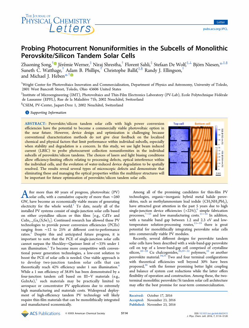
(SHJ) tandem solar cells (Figure 1a), prepared as previouslyreported,28 were used for this study. In brief, these tandem cellsconsisted of a front-emitter SHJ bottom cell based on a double-side-polished (DSP) wafer, an indium zinc oxide (IZO)intermediate recombination layer, and a CH3NH3PbI3 perov-skite top cell with polyethylenimine ethoxylated (PEIE)/phenyl-C60-butyric acid methyl ester (PCBM) and 2,2′,7,7′-tetrakis(N,N-di-4-methoxyphenylamino)-9,9′-spirobifluorene(spiro-OMeTAD) electron and hole transport layers, respec-tively. The transparent front electrode was composed of aMoOx buffer layer and a bilayer of hydrogenated indium oxide(IO:H) and indium tin oxide (ITO). To quantify thephotocurrent in the individual subcells, we measured theEQE of each subcell and the optical reflectance and J−V curve
of the entire device (Figures 1b,c). Some factors limiting thephotocurrent of the subcells can be identified from the spectra.For the top cell, the overall EQE (∼70% maximum) is less thanthe state-of-art transparent perovskite cells (>80%),27 likely dueto the presence of defects in the solution-processed layers (videinfra). At longer wavelengths (>850 nm), strong opticalinterference effects give rise to modulations in the reflectivitywith complementary reductions in the EQE.To gain further insight, a custom LBIC system was used to
spatially resolve current generation in the tandem cells.42 Laserlight at different wavelengths (532 and 1064 nm) and at arelatively low power density (∼800 mW/cm2, to avoid possibleillumination damage of the perovskite cell)43 was used to excitecharge carriers in the perovskite and Si subcells. Thephotogenerated current was calibrated for EQE to constructLBIC maps using a reference photodiode (Figure S1). A biaslight with a controlled optical spectrum was applied toselectively generate carriers in only one of the subcells44 sothat the LBIC of the entire device was limited by the laser-generated current in the measured subcell (see the Exper-imental Methods section for details).Figure 2 shows LBIC maps for a tandem device probed with
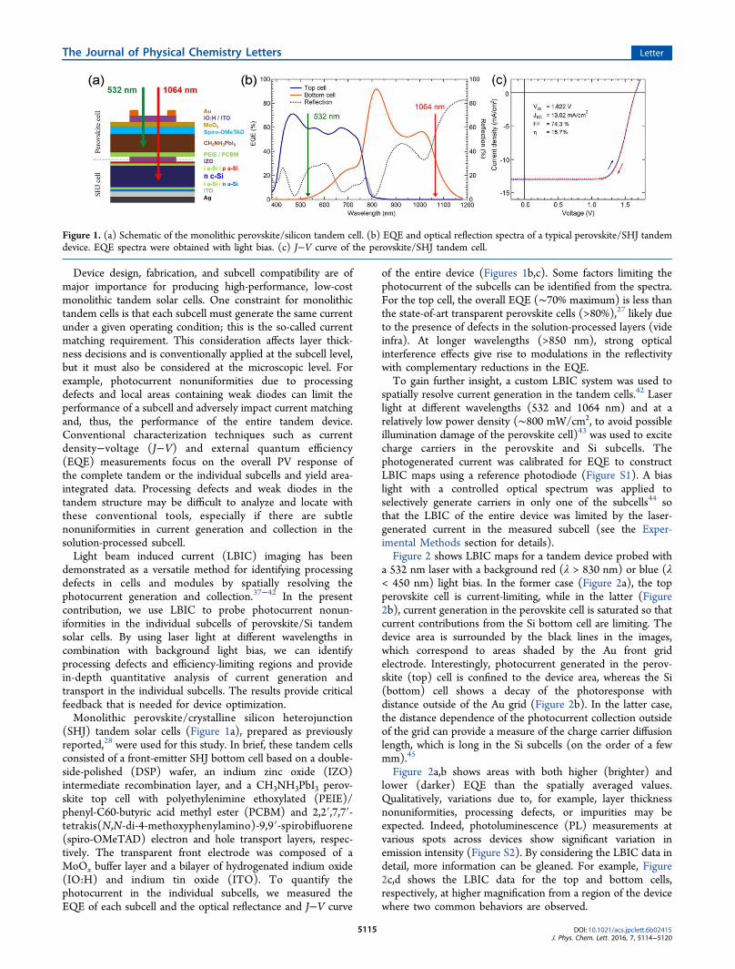
a 532 nm laser with a background red (λ > 830 nm) or blue (λ< 450 nm) light bias. In the former case (Figure 2a), the topperovskite cell is current-limiting, while in the latter (Figure2b), current generation in the perovskite cell is saturated so thatcurrent contributions from the Si bottom cell are limiting. Thedevice area is surrounded by the black lines in the images,which correspond to areas shaded by the Au front gridelectrode. Interestingly, photocurrent generated in the perov-skite (top) cell is confined to the device area, whereas the Si(bottom) cell shows a decay of the photoresponse withdistance outside of the Au grid (Figure 2b). In the latter case,the distance dependence of the photocurrent collection outsideof the grid can provide a measure of the charge carrier diffusionlength, which is long in the Si subcells (on the order of a fewmm).45
Figure 2a,b shows areas with both higher (brighter) andlower (darker) EQE than the spatially averaged values.Qualitatively, variations due to, for example, layer thicknessnonuniformities, processing defects, or impurities may beexpected. Indeed, photoluminescence (PL) measurements atvarious spots across devices show significant variation inemission intensity (Figure S2). By considering the LBIC data indetail, more information can be gleaned. For example, Figure2c,d shows the LBIC data for the top and bottom cells,respectively, at higher magnification from a region of the devicewhere two common behaviors are observed.
Figure 1. (a) Schematic of the monolithic perovskite/silicon tandem cell. (b) EQE and optical reflection spectra of a typical perovskite/SHJ tandemdevice. EQE spectra were obtained with light bias. (c) J−V curve of the perovskite/SHJ tandem cell.
The Journal of Physical Chemistry Letters Letter
DOI: 10.1021/acs.jpclett.6b02415J. Phys. Chem. Lett. 2016, 7, 5114−5120
Area 1 shows a common type of defect in which thephotocurrent is reduced in both the top and bottom cells.These 100−200 μm features are ubiquitous. Note that thecollection properties of the top cell and the interconnectionbetween cells at the defect site are irrelevant to currentcollection from the bottom cell because the long carrier
diffusion lengths in the Si would allow current to be collectedaway from the defect if the underlying Si were indeedphotoexcited. Scanning electron microscopy and elementalanalysis revealed several different types of defects (Figure S3),and each one was found to be deficient in either Pb, Si, N, or I.We can speculate that the defect in Area 1 is related to a light-blocking impurity particle or component aggregate that wasintroduced during solution-based processing of the PEIE/PCBM, spiro-OMeTAD, or perovskite layers. It is unlikely thatsuch a large particle could be introduced through the air duringprocessing because the samples are handled in a clean roomenvironment. Figure 2e,f shows distribution histograms for theLBIC data from Area 1 in comparison to the area-averaged datafor the device. Clearly, higher performance for the tandemcould be achieved if these defects could be eliminated. Thismight be achieved by simply adjusting the solubility/viscosity ofthe solution or by filtering prior to deposition.Area 2 in Figure 2c,d shows another type of behavior. Here, a
comet streak is seen where the EQE is enhanced in both thetop and bottom cells. At least eight features like this areobserved in Figure 2a,b. The orientation of the features, withthe half-ellipse pointing toward the rotational axis of the sampleduring spinning, makes it clear that these features are developedduring a spinning process. Possible origins include heightvariation in an underlying layer that could affect thehydrodynamics of material distribution during a spinning stepor use of a precursor solution with nonuniform viscosity.Variations in the perovskite film thickness are not expected tobe responsible for this behavior because such variations shouldimpact the EQE from the top and bottom cells oppositely, asexplained below. Thus, we are left with assigning the features tobehavior associated with spinning application of the spiro-OMeTAD. Note that the comet-shaped defect is anchored on adefect like the one found in Area 1. Interestingly, the thicknessvariation of the spiro-OMeTAD creates a local variation in thefilm thickness, as shown in the optical microscopic image(Figure S4). Clearly, more study of these “defects” is warranted;the data in Figure 2h,g suggest that the overall device efficiencycould be significantly enhanced if the EQE benefits could beharvested across the entire device area.
Figure 2. LBIC maps of the top (a,c) and bottom (b,d) cells of atypical perovskite/silicon tandem solar cell probed with a 532 nm laserlight under red or blue light bias, respectively. Histograms ofphotocurrent distribution from two selected areas (1 and 2 in panelsc and d) that show different behaviors for the top (e,g) and bottom(f,h) cells. The dashed curves in the histograms show the currentdistribution averaged across the device area.
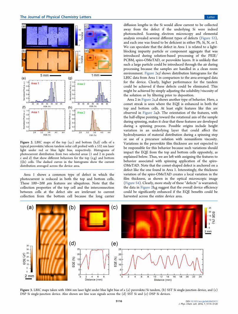
Figure 3. LBIC maps taken with 1064 nm laser light under blue light bias of a (a) perovskite/Si tandem, (b) SST Si single-junction device, and (c)DSP Si single-junction device. Also shown are line scan signals across the (d) SST Si and (e) DSP Si devices.
The Journal of Physical Chemistry Letters Letter
DOI: 10.1021/acs.jpclett.6b02415J. Phys. Chem. Lett. 2016, 7, 5114−5120
Another type of defect (Figure S5) shows a local reduction inthe photocurrent in the top cell and a corresponding increase inthe bottom cell. This can be explained by considering that thesolution-processed perovskite layer may be locally thin, missing,or degraded,37,46 such that light absorption in the perovskitecell is decreased. Reduced absorption in the top cell wouldallow more light to pass through, leading to more photocurrentgeneration in the bottom cell. Additionally, reduced thicknessor incomplete coverage of the perovskite layer may introducelocal shunts in the top cell, improving the transport of chargecarriers generated in the bottom cell. To ameliorate this type ofdefect, the formation of a compact and phase-pure perovskitelayer should be precisely controlled.46
Similar LBIC analyses were performed on other devices withsmall (0.17 cm2) and large (1.22 cm2) areas (Figures S6 andS7). As expected, the large-area devices generally exhibitedmore severe current nonuniformities than the smaller ones.Quantifying the LBIC results shows that if all top cell defectscould be eliminated by optimization of the processing andoptical design, the overall current generation in the perovskitecell could be improved by up to 3 mA/cm2, which would boostthe efficiency of that tandem cell from ∼16 to ∼19% (FigureS8)The LBIC maps obtained with the 1064 nm laser reveal new,
interesting behaviors (Figure 3a). No signal was collected fromthe top cell because the perovskite subcell is transparent to1064 nm light. In the bottom cell, however, although there isevidence for the same defects observed using the 532 nm laserlight (Figure 2d), optical interference fringes were dominant(Figure 3a). The patterns persisted after the sample was rotatedor moved relative to the laser beam’s axis (Figure S9),indicating that the optical fringes originated from the devicestructure. The fringes are most likely caused by the non-parallelism of the two mirror polished surfaces of the siliconbottom cell.45 Analysis of the optical path length betweenadjacent maxima shows that the nonparallelism from fringemaximum to fringe maximum is ∼0.6 μm (SupportingInformation). This variation arises due to the particular DSPSi wafers (260−300 μm thickness) that were used with aspecified total thickness variation of 5−10 μm across wafers.To confirm the origin of the optical fringes, we compared the
LBIC maps of two SHJ cells that were prepared with single-side-textured (SST) and DSP surfaces. It is notable that thebottom cells with front surface texture are not currentlycompatible with solution processing of the perovskite cells;thus, only the back surface of the SHJ cell can be textured withrandom pyramids. The SST cell (Figure 3b) exhibits a high anduniform photocurrent over the active area. The DSP cell(Figure 3c), on the contrary, shows optical interferencepatterns similar to those of the perovskite/Si tandem device.To quantify the photocurrent nonuniformities caused by opticalinterference of the bottom cells, the line scan profiles of thesetwo devices are shown in Figure 3d,e. The peak-to-peakvariations of photocurrent generated by the 1064 nm laser inthe SST and DSP cells are 5 and 36%, respectively. The largevariation in the DSP cell indicates that the tandem devicesusing the DSP bottom cells suffer a significant monochromaticefficiency loss due to the absence of light trapping, which isqualitatively consistent with the EQE spectra of the tandemdevice (Figure 1b). This optical loss can be recovered by theaddition of an antireflective coating (e.g., MgF2) or micro-textured foil47 to the device and/or the use of the textured backsurface of bottom cells.27
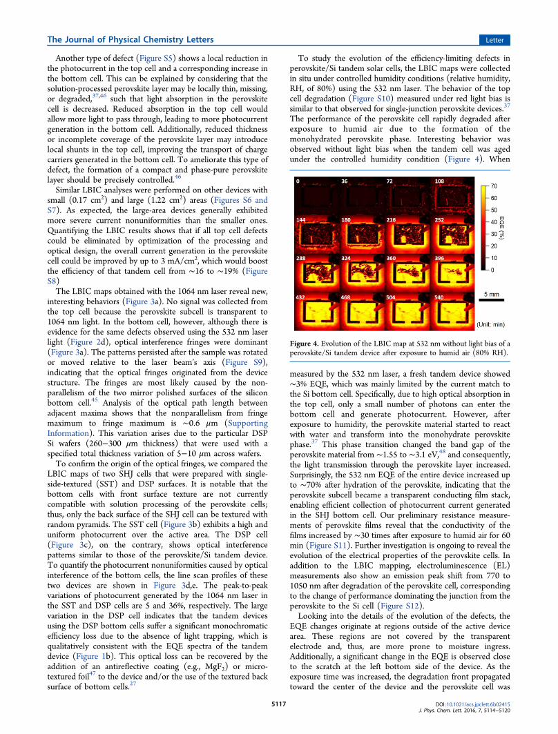
To study the evolution of the efficiency-limiting defects inperovskite/Si tandem solar cells, the LBIC maps were collectedin situ under controlled humidity conditions (relative humidity,RH, of 80%) using the 532 nm laser. The behavior of the topcell degradation (Figure S10) measured under red light bias issimilar to that observed for single-junction perovskite devices.37
The performance of the perovskite cell rapidly degraded afterexposure to humid air due to the formation of themonohydrated perovskite phase. Interesting behavior wasobserved without light bias when the tandem cell was agedunder the controlled humidity condition (Figure 4). When
measured by the 532 nm laser, a fresh tandem device showed∼3% EQE, which was mainly limited by the current match tothe Si bottom cell. Specifically, due to high optical absorption inthe top cell, only a small number of photons can enter thebottom cell and generate photocurrent. However, afterexposure to humidity, the perovskite material started to reactwith water and transform into the monohydrate perovskitephase.37 This phase transition changed the band gap of theperovskite material from ∼1.55 to ∼3.1 eV,48 and consequently,the light transmission through the perovskite layer increased.Surprisingly, the 532 nm EQE of the entire device increased upto ∼70% after hydration of the perovskite, indicating that theperovskite subcell became a transparent conducting film stack,enabling efficient collection of photocurrent current generatedin the SHJ bottom cell. Our preliminary resistance measure-ments of perovskite films reveal that the conductivity of thefilms increased by ∼30 times after exposure to humid air for 60min (Figure S11). Further investigation is ongoing to reveal theevolution of the electrical properties of the perovskite cells. Inaddition to the LBIC mapping, electroluminescence (EL)measurements also show an emission peak shift from 770 to1050 nm after degradation of the perovskite cell, correspondingto the change of performance dominating the junction from theperovskite to the Si cell (Figure S12).Looking into the details of the evolution of the defects, the
EQE changes originate at regions outside of the active devicearea. These regions are not covered by the transparentelectrode and, thus, are more prone to moisture ingress.Additionally, a significant change in the EQE is observed closeto the scratch at the left bottom side of the device. As theexposure time was increased, the degradation front propagatedtoward the center of the device and the perovskite cell was
Figure 4. Evolution of the LBIC map at 532 nm without light bias of aperovskite/Si tandem device after exposure to humid air (80% RH).
The Journal of Physical Chemistry Letters Letter
DOI: 10.1021/acs.jpclett.6b02415J. Phys. Chem. Lett. 2016, 7, 5114−5120
completely degraded after ∼480 min. The observations areconsistent with recent findings by Bush et al. that show that theimpacts of moisture can be mitigated to some degree bycombining a compact ITO layer, a hydrophobic chargetransport layer, and more stable perovskite compositions.24
In summary, we used LBIC combined with light bias toprobe photocurrent nonuniformities within the subcells ofhigh-efficiency perovskite/Si tandem devices. A variety ofphenomena including light-blocking, defects, and potentialenhancements were observed. Strong optical interferenceintroduced by 1064 nm laser light was observed when DSPbottom cells were used. This optical loss can be mitigated bydeveloping tandems on the textured SHJ cells. Additionally, weobserved the evolution of a LBIC map of a tandem device afterexposure to humid air, showing the importance of protectingthe device from water ingress. For full realization of the promiseof high-efficiency perovskite/Si tandems, management of thematerial uniformity, interface integrity, current collection andgeneration, and optics of the interfaces and layers will beessential.
■ EXPERIMENTAL METHODSDevice Fabrication. The perovskite/silicon tandem solar cellswere fabricated following a previously published method.28 Inbrief, a DSP n-type-doped silicon wafer was used to prepare aSHJ solar cell, serving as the bottom cell for the tandems. A 40nm IZO was sputtered on the front side of the silicon bottomcells to act as a recombination layer. Then, the perovskite topcell was deposited as follows. The electron contact wasprepared by spin-coating of a PEIE/PCBM bilayer. Theperovskite absorber layer was fabricated with a hybridsequential method, consisting of an evaporated 150 nm PbI2layer subsequently transformed in the perovskite phase by spincoating a 50 mg/mL methylammonium iodide solution. Thehole contact was prepared by spin coating of spiro-OMeTADsolution. The transparent front electrode was deposited bythermal evaporation of a 10 nm MoOx buffer layer, followed bysputtering of a bilayer of 110 nm IO:H/ITO. A 100 nm goldframe was finally evaporated through a shadow mask.LBIC Measurement. The LBIC system as previously reported
was used to spatially resolve the current collection efficiencymap.42 Nd:YAG lasers at 532 and 1064 nm operating in the Q-switching mode were used to generate a light beam with anaverage power of 0.01 mW and a 40 μm diameter. The laserbeam was used to scan across the tandem solar cells at a speedof 1 mm/s with a 30 μm spacing between two lateral scans. Thephotocurrent was collected by a Keithley 2601 source meter atan acquisition rate of 5 kHz and converted into local externalquantum efficiencies using a reference Si photodiode (Model:S2281-8D083) with a calibrated EQE (Figure S1). The top/bottom cell was measured with infrared/blue (λ > 830 nm/<450 nm) light bias generated using a white 100 W light sourcewith the corresponding long/short wavelength pass opticalfilter. The procedure for the in situ degradation study wassimilar to that in our previous work.37
Other Characterization Methods. EQE spectra were obtainedfrom 320 to 1150 nm (PV Measurements IVQUE8-C) with thesame light bias conditions as that in the LBIC measurements.J−V curves were measured using a Keithley 2440 source meterand a solar simulator (Newport model 91195A-1000)calibrated to simulate AM1.5 illumination. The opticalreflection spectrum was measured by a UV−vis spectrometer(PerkinElmer Lambda 1050) in the range of 350−2000 nm.
Scanning electron microscopic (SEM) images and energy-dispersive X-ray (EDX) spectroscopy were obtained using afield emission electron microscope (Hitachi S-4800). The PL/EL measurements were recorded (integration time = 0.5 s) by aHoriba Symphony-II CCD detector after a 300 g/mm gratingmonochromator (iHR-320). For PL measurement, a 532 nmcw laser beam (beam diameter ≈ 84 μm) at 79 mW/cm2 wasused as a source of excitation for steady state. For ELmeasurement, a tandem solar cell was forward biased whilemonitoring the applied voltage. The resistance of the perovskitefilms was measured using a Keithley 2601 source meter bysweeping the voltage from −20 to 20 V and recording thecurrent.
■ ASSOCIATED CONTENT*S Supporting InformationThe Supporting Information is available free of charge on theACS Publications website at DOI: 10.1021/acs.jpclett.6b02415.
LBIC to EQE calibration; PL spectra; SEM and EDXanalysis on defects; LBIC analysis of a particular defect;LBIC maps of cells with different areas; LBIC statistics ofcells with different areas; quantifying the potentialcurrent improvement; LBIC maps of optical interference;interference path length calculation; degradation of theperovskite top cell; resistivity evolution of a perovskitefilm; EL of tandem cells before and after degradation(PDF)
■ AUTHOR INFORMATIONCorresponding Authors*E-mail: [email protected] (B.N.).*E-mail: [email protected] (M.J.H.).ORCIDZhaoning Song: 0000-0002-6677-0994Michael J. Heben: 0000-0002-3788-3471Present Address⊥S.D.W.: King Abdullah University of Science and Technology(KAUST), KAUST Solar Center (KSC), Thuwal 23955-6900,Saudi Arabia.NotesThe authors declare no competing financial interest.
■ ACKNOWLEDGMENTSThis work is financially supported by the Wright CenterEndowment for Photovoltaics Innovation and Commercializa-tion, U.S. Air Force Research Laboratory, Space VehiclesDirectorate (Contract No. FA9453-11-C-0253), U.S. NationalScience Foundation (Contract No. CHE-1230246), SwissNational Science Foundation, Nano-Tera.ch, and Swiss FederalOffice of Energy, under Grant SI/501072-01.
■ REFERENCES(1) Fraunhofer Institute for Solar Energy Systems Photovoltaic Report.https://www.ise.fraunhofer.de/en/downloads-englisch/pdf-files-englisch/photovoltaics-report-slides.pdf (accessed 11 October 2016).(2) Jean, J.; Brown, P. R.; Jaffe, R. L.; Buonassisi, T.; Bulovic, V.Pathways for Solar Photovoltaics. Energy Environ. Sci. 2015, 8, 1200−1219.(3) Shockley, W.; Queisser, H. J. Detailed Balance Limit of Efficiencyof p-n Junction Solar Cells. J. Appl. Phys. 1961, 32, 510−519.(4) Vos, A. D. Detailed Balance Limit of the Efficiency of TandemSolar Cells. J. Phys. D: Appl. Phys. 1980, 13, 839.
The Journal of Physical Chemistry Letters Letter
DOI: 10.1021/acs.jpclett.6b02415J. Phys. Chem. Lett. 2016, 7, 5114−5120
(5) Green, M. A.; Emery, K.; Hishikawa, Y.; Warta, W.; Dunlop, E. D.Solar Cell Efficiency Tables (Version 48). Prog. Photovoltaics 2016, 24,905−913.(6) Yang, W. S.; Noh, J. H.; Jeon, N. J.; Kim, Y. C.; Ryu, S.; Seo, J.;Seok, S. I. High-Performance Photovoltaic Perovskite LayersFabricated through Intramolecular Exchange. Science 2015, 348,1234−1237.(7) Lee, M. M.; Teuscher, J.; Miyasaka, T.; Murakami, T. N.; Snaith,H. J. Efficient Hybrid Solar Cells Based on Meso-SuperstructuredOrganometal Halide Perovskites. Science 2012, 338, 643−647.(8) Burschka, J.; Pellet, N.; Moon, S.-J.; Humphry-Baker, R.; Gao, P.;Nazeeruddin, M. K.; Graetzel, M. Sequential Deposition as a Route toHigh-Performance Perovskite-Sensitized Solar Cells. Nature 2013,499, 316−319.(9) Song, Z.; Watthage, S. C.; Phillips, A. B.; Heben, M. J. Pathwaystoward High-Performance Perovskite Solar Cells: Review of RecentAdvances in Organo-Metal Halide Perovskites for PhotovoltaicApplications. J. Photonics Energy 2016, 6, 022001.(10) Li, X.; Bi, D.; Yi, C.; Decoppet, J.-D.; Luo, J.; Zakeeruddin, S.M.; Hagfeldt, A.; Gratzel, M. A Vacuum Flash−Assisted SolutionProcess for High-Efficiency Large-Area Perovskite Solar Cells. Science2016, 353, 58.(11) Snaith, H. J. Perovskites: The Emergence of a New Era for Low-Cost, High-Efficiency Solar Cells. J. Phys. Chem. Lett. 2013, 4, 3623−3630.(12) Gao, P.; Gratzel, M.; Nazeeruddin, M. K. Organohalide LeadPerovskites for Photovoltaic Applications. Energy Environ. Sci. 2014, 7,2448−2463.(13) Green, M. A.; Ho-Baillie, A.; Snaith, H. J. The Emergence ofPerovskite Solar Cells. Nat. Photonics 2014, 8, 506−514.(14) Gong, J.; Darling, S. B.; You, F. Perovskite Photovoltaics: Life-Cycle Assessment of Energy and Environmental Impacts. EnergyEnviron. Sci. 2015, 8, 1953−1968.(15) Zhang, W.; Anaya, M.; Lozano, G.; Calvo, M. E.; Johnston, M.B.; Míguez, H.; Snaith, H. J. Highly Efficient Perovskite Solar Cellswith Tunable Structural Color. Nano Lett. 2015, 15, 1698−1702.(16) Sutton, R. J.; Eperon, G. E.; Miranda, L.; Parrott, E. S.; Kamino,B. A.; Patel, J. B.; Horantner, M. T.; Johnston, M. B.; Haghighirad, A.A.; Moore, D. T.; et al. Bandgap-Tunable Cesium Lead HalidePerovskites with High Thermal Stability for Efficient Solar Cells. Adv.Energy Mater. 2016, 6, 1502458.(17) Xing, G.; Mathews, N.; Lim, S. S.; Yantara, N.; Liu, X.; Sabba,D.; Gratzel, M.; Mhaisalkar, S.; Sum, T. C. Low-TemperatureSolution-Processed Wavelength-Tunable Perovskites for Lasing. Nat.Mater. 2014, 13, 476−480.(18) Noh, J. H.; Im, S. H.; Heo, J. H.; Mandal, T. N.; Seok, S. I.Chemical Management for Colorful, Efficient, and Stable Inorganic-Organic Hybrid Nanostructured Solar Cells. Nano Lett. 2013, 13,1764−1769.(19) Liao, W.; Zhao, D.; Yu, Y.; Shrestha, N.; Ghimire, K.; Grice, C.R.; Wang, C.; Xiao, Y.; Cimaroli, A. J.; Ellingson, R. J.; et al.Fabrication of Efficient Low-Bandgap Perovskite Solar Cells byCombining Formamidinium Tin Iodide with MethylammoniumLead Iodide. J. Am. Chem. Soc. 2016, 138, 12360−12363.(20) Bailie, C. D.; Christoforo, M. G.; Mailoa, J. P.; Bowring, A. R.;Unger, E. L.; Nguyen, W. H.; Burschka, J.; Pellet, N.; Lee, J. Z.;Gratzel, M.; et al. Semi-Transparent Perovskite Solar Cells forTandems with Silicon and CIGS. Energy Environ. Sci. 2015, 8, 956−963.(21) Mailoa, J. P.; Bailie, C. D.; Johlin, E. C.; Hoke, E. T.; Akey, A. J.;Nguyen, W. H.; McGehee, M. D.; Buonassisi, T. A 2-TerminalPerovskite/Silicon Multijunction Solar Cell Enabled by a SiliconTunnel Junction. Appl. Phys. Lett. 2015, 106, 121105.(22) Loper, P.; Moon, S.-J.; Martin de Nicolas, S.; Niesen, B.;Ledinsky, M.; Nicolay, S.; Bailat, J.; Yum, J.-H.; De Wolf, S.; Ballif, C.Organic-Inorganic Halide Perovskite/Crystalline Silicon Four-Termi-nal Tandem Solar Cells. Phys. Chem. Chem. Phys. 2015, 17, 1619−1629.
(23) Albrecht, S.; Saliba, M.; Correa Baena, J. P.; Lang, F.;Kegelmann, L.; Mews, M.; Steier, L.; Abate, A.; Rappich, J.; Korte,L.; et al. Monolithic Perovskite/Silicon-Heterojunction Tandem SolarCells Processed at Low Temperature. Energy Environ. Sci. 2016, 9, 81−88.(24) Bush, K. A.; Bailie, C. D.; Chen, Y.; Bowring, A. R.; Wang, W.;Ma, W.; Leijtens, T.; Moghadam, F.; McGehee, M. D. Thermal andEnvironmental Stability of Semi-Transparent Perovskite Solar Cells forTandems Enabled by a Solution-Processed Nanoparticle Buffer Layerand Sputtered Ito Electrode. Adv. Mater. 2016, 28, 3937−3943.(25) Chen, B.; Bai, Y.; Yu, Z.; Li, T.; Zheng, X.; Dong, Q.; Shen, L.;Boccard, M.; Gruverman, A.; Holman, Z.; et al. Efficient Semi-transparent Perovskite Solar Cells for 23.0%-Efficiency Perovskite/Silicon Four-Terminal Tandem Cells. Adv. Energy Mater. 2016, 6,1601128.(26) McMeekin, D. P.; Sadoughi, G.; Rehman, W.; Eperon, G. E.;Saliba, M.; Horantner, M. T.; Haghighirad, A.; Sakai, N.; Korte, L.;Rech, B.; et al. A Mixed-Cation Lead Mixed-Halide PerovskiteAbsorber for Tandem Solar Cells. Science 2016, 351, 151−155.(27) Werner, J.; Barraud, L.; Walter, A.; Brauninger, M.; Sahli, F.;Sacchetto, D.; Tetreault, N.; Paviet-Salomon, B.; Moon, S.-J.; Allebe,C.; et al. Efficient near-Infrared-Transparent Perovskite Solar CellsEnabling Direct Comparison of 4-Terminal and Monolithic Perov-skite/Silicon Tandem Cells. ACS Energy Lett. 2016, 1, 474−480.(28) Werner, J.; Weng, C.-H.; Walter, A.; Fesquet, L.; Seif, J. P.; DeWolf, S.; Niesen, B.; Ballif, C. Efficient Monolithic Perovskite/SiliconTandem Solar Cell with Cell Area > 1 cm2. J. Phys. Chem. Lett. 2016, 7,161−166.(29) Todorov, T.; Gershon, T.; Gunawan, O.; Sturdevant, C.; Guha,S. Perovskite-Kesterite Monolithic Tandem Solar Cells with HighOpen-Circuit Voltage. Appl. Phys. Lett. 2014, 105, 173902.(30) Todorov, T.; Gershon, T.; Gunawan, O.; Lee, Y. S.; Sturdevant,C.; Chang, L.-Y.; Guha, S. Monolithic Perovskite-CIGS Tandem SolarCells via in situ Band Gap Engineering. Adv. Energy Mater. 2015, 5,1500799.(31) Kranz, L.; Abate, A.; Feurer, T.; Fu, F.; Avancini, E.; Lockinger,J.; Reinhard, P.; Zakeeruddin, S. M.; Gratzel, M.; Buecheler, S.; et al.High-Efficiency Polycrystalline Thin Film Tandem Solar Cells. J. Phys.Chem. Lett. 2015, 6, 2676−2681.(32) Fu, F.; Feurer, T.; Jager, T.; Avancini, E.; Bissig, B.; Yoon, S.;Buecheler, S.; Tiwari, A. N. Low-Temperature-Processed EfficientSemi-Transparent Planar Perovskite Solar Cells for Bifacial andTandem Applications. Nat. Commun. 2015, 6, 8932.(33) Liu, Y.; Renna, L. A.; Bag, M.; Page, Z. A.; Kim, P.; Choi, J.;Emrick, T.; Venkataraman, D.; Russell, T. P. High Efficiency TandemThin-Perovskite/Polymer Solar Cells with a Graded RecombinationLayer. ACS Appl. Mater. Interfaces 2016, 8, 7070−7076.(34) Yang, Z.; Rajagopal, A.; Chueh, C.-C.; Jo, S. B.; Liu, B.; Zhao,T.; Jen, A. K. Y. Stable Low-Bandgap Pb−Sn Binary Perovskites forTandem Solar Cells. Adv. Mater. 2016, 28, 8990−8997.(35) Eperon, G. E.; Leijtens, T.; Bush, K. A.; Green, T.; Wang, J. T.-W.; McMeekin, D. P.; Volonakis, G. Perovskite-Perovskite TandemPhotovoltaics with Ideal Bandgaps. ArXiv 2016, https://arxiv.org/abs/1608.03920.(36) Bailie, C. D.; McGehee, M. D. High-Efficiency TandemPerovskite Solar Cells. MRS Bull. 2015, 40, 681−686.(37) Song, Z.; Abate, A.; Watthage, S. C.; Liyanage, G. K.; Phillips, A.B.; Steiner, U.; Graetzel, M.; Heben, M. J. Perovskite Solar CellStability in Humid Air: Partially Reversible Phase Transitions in thePbI2-CH3NH3I-H2O System. Adv. Energy Mater. 2016, 6, 1600846.(38) Vorasayan, P.; Betts, T. R.; Tiwari, A. N.; Gottschalg, R. Multi-Laser LBIC System for Thin Film PV Module Characterisation. Sol.Energy Mater. Sol. Cells 2009, 93, 917−921.(39) Krebs, F. C.; Jørgensen, M. 2D Characterization of OPV fromSingle and Tandem Cells to Fully Roll-to-Roll Processed Moduleswith and without Electrical Contact. Adv. Opt. Mater. 2014, 2, 465−477.(40) Larsen-Olsen, T. T.; Andersen, T. R.; Dam, H. F.; Jørgensen,M.; Krebs, F. C. Probing Individal Subcells of Fully Printed and
The Journal of Physical Chemistry Letters Letter
DOI: 10.1021/acs.jpclett.6b02415J. Phys. Chem. Lett. 2016, 7, 5114−5120
Coated Polymer Tandem Solar Cells Using Multichromatic Opto-Electronic Characterization Methods. Sol. Energy Mater. Sol. Cells2015, 137, 154−163.(41) Reinhardt, J.; Apilo, P.; Zimmermann, B.; Rousu, S.; Wurfel, U.Determining the Photocurrent of Individual Cells within an OrganicSolar Module by LBIC and the Filtering Approach: Experiments andSimulations. Sol. Energy Mater. Sol. Cells 2015, 134, 157−164.(42) Phillips, A. B.; Song, Z.; DeWitt, J. L.; Stone, J. M.; Krantz, P.W.; Royston, J. M.; Zeller, R. M.; Mapes, M. R.; Roland, P. J.; Dorogi,M. D.; et al. High Speed, Intermediate Resolution, Large Area LaserBeam Induced Current Imaging and Laser Scribing System forPhotovoltaic Devices and Modules. Rev. Sci. Instrum. 2016, 87, 093708.(43) Ledinsky, M.; Loper, P.; Niesen, B.; Holovsky, J.; Moon, S.-J.;Yum, J.-H.; De Wolf, S.; Fejfar, A.; Ballif, C. Raman Spectroscopy ofOrganic−Inorganic Halide Perovskites. J. Phys. Chem. Lett. 2015, 6,401−406.(44) Meusel, M.; Baur, C.; Letay, G.; Bett, A. W.; Warta, W.;Fernandez, E. Spectral Response Measurements of Monolithic GaInP/Ga(In)As/Ge Triple-Junction Solar Cells: Measurement Artifacts andTheir Explanation. Prog. Photovoltaics 2003, 11, 499−514.(45) Holovsky, J.; De Wolf, S.; Jirícek, P.; Ballif, C. Attenuated TotalReflectance Fourier-Transform Infrared Spectroscopic Investigation ofSilicon Heterojunction Solar Cells. Rev. Sci. Instrum. 2015, 86, 073108.(46) Song, Z.; Watthage, S. C.; Phillips, A. B.; Tompkins, B. L.;Ellingson, R. J.; Heben, M. J. Impact of Processing Temperature andComposition on the Formation of Methylammonium Lead IodidePerovskites. Chem. Mater. 2015, 27, 4612−4619.(47) Ulbrich, C.; Gerber, A.; Hermans, K.; Lambertz, A.; Rau, U.Analysis of Short Circuit Current Gains by an Anti-Reflective TexturedCover on Silicon Thin Film Solar Cells. Prog. Photovoltaics 2013, 21,1672−1681.(48) Leguy, A. M. A.; Hu, Y.; Campoy-Quiles, M.; Alonso, M. I.;Weber, O. J.; Azarhoosh, P.; van Schilfgaarde, M.; Weller, M. T.; Bein,T.; Nelson, J.; et al. Reversible Hydration of CH3NH3PbI3 in Films,Single Crystals, and Solar Cells. Chem. Mater. 2015, 27, 3397−3407.
The Journal of Physical Chemistry Letters Letter
DOI: 10.1021/acs.jpclett.6b02415J. Phys. Chem. Lett. 2016, 7, 5114−5120