Probing the conductance superposition lawin single-molecule circuits with parallel pathsH. Vazquez1‡, R. Skouta2‡, S. Schneebeli2, M. Kamenetska1†, R. Breslow2*, L. Venkataraman1*and M.S. Hybertsen3*
According to Kirchhoff ’s circuit laws, the net conductance oftwo parallel components in an electronic circuit is the sum ofthe individual conductances. However, when the circuit dimen-sions are comparable to the electronic phase coherence length,quantum interference effects play a critical role1, as exemplifiedby the Aharonov–Bohm effect in metal rings2,3. At the molecu-lar scale, interference effects dramatically reduce the electrontransfer rate through a meta-connected benzene ring whencompared with a para-connected benzene ring4,5. For longerconjugated and cross-conjugated molecules, destructive inter-ference effects have been observed in the tunnelling conduc-tance through molecular junctions6–10. Here, we investigatethe conductance superposition law for parallel components insingle-molecule circuits, particularly the role of interference.We synthesize a series of molecular systems that containeither one backbone or two backbones in parallel, bondedtogether cofacially by a common linker on each end. Single-mol-ecule conductance measurements and transport calculationsbased on density functional theory show that the conductanceof a double-backbone molecular junction can be more thantwice that of a single-backbone junction, providing clear evi-dence for constructive interference.
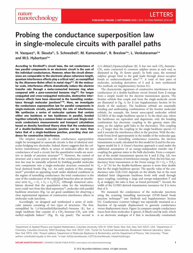
The simplest example in which conductance superpositionmight be investigated in nanoscale circuits is that of identical mol-ecules bridging two electrodes. Indeed, theory suggests that the col-lective (interference) effects in arrays of molecules affect the netconductance of such a circuit, but the quantitative results are sensi-tive to details of junction structure11–16. However, the control ofstructure and a more precise probe of the conductance superposi-tion law may be naturally achieved by building parallel molecularwire components into a single-molecular structure connected bylocal chemical bonds (Fig. 1a). An early analysis of this arrange-ment12 provided an appealing result under idealized conditions inthe regime of tunnelling conductance: the total conductance is thesum of the conductance of the individual branches plus an interfer-ence term Gtot = G1 + G2 + 2
������G1G2
√. Although numerical calcu-
lations showed that the quantitative value for the interferenceterm could vary from this ideal expression12, molecules with parallelbackbone structures (Fig. 1a) are good candidates for observing aclear experimental signature of constructive interference effects inmolecular-scale junctions.
Accordingly, we designed and synthesized a series of mole-cular systems consisting of two types of structures. The first,exemplified by 1,4-bis(methyl(thio)methyl)–benzene (1), has asingle backbone that consists of a CH2–benzene–CH2 unit withmethyl-sulphide linkers17 (Fig. 1b, top panel). The second is
2,11-dithia(3,3)paracyclophane (2). It has two such CH2–benzene–CH2 units connected to common sulphur atoms at each end, asillustrated in Fig. 1b (lower panel). In both cases, the terminalsulphur groups bind to the gold leads through donor–acceptorbonds to undercoordinated sites17,18. A total of four pairs ofmolecules, including derivatives of 1 and 2, were synthesized(for methods see Supplementary Section S1).
The characteristic signatures of constructive interference in theconductance of a double-backbone circuit formed from 2 emergefrom a simple model for the electron transmission spectra. Thefrontier orbitals that couple and form the single-molecule circuitare illustrated in Fig. 1c for 2 (see Supplementary Section S4 fordetails of the analysis). The backbone orbitals are essentiallybonding and antibonding combinations of the frontier molecularorbitals, for example, the lowest unoccupied molecular orbital(LUMO) of the single-backbone species 1. In the ideal case, wherethe backbones are equivalent and degenerate, only the bondingcombination has electronic coupling to the gateway states (thestates on the sulphur–gold links to the electrodes). This couplingis
��2
√larger than the coupling in the single-backbone species (t)
and it encodes the interference effect in the junction. With the elec-trode Fermi level approximately in the middle of the molecular gap,characteristic of tunnelling conductance scenarios, the electrontransmission is easily calculated for this model for 2 and for the ana-logous model for 1. A Green’s function approach is used under theadditional assumption of an energy-independent transfer rate G
coupling the gateway states to the bulk electrodes. From a compari-son of the model transmission spectra for 1 and 2 (Fig. 1d), twocharacteristic features of interference emerge. First, the low bias con-ductance from transmission at the Fermi energy (G¼G0 × T(EF),G0¼ 2e2/h) for the double-backbone species is more than doublethat for the single-backbone species. The specific value of the con-ductance ratio G(2)/G(1) depends on the details, but in the mostidealized limit (degenerate backbone levels with small throughspace coupling, vanishing t, large and energy-independent G andEF at midgap), the ratio is four, as found previously12. Second, thewidth of the LUMO-derived transmission resonance for 2 is twicethat of 1.
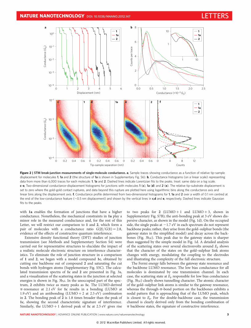
We measured the conductance of the molecular junctionsusing the scanning tunnelling microscope (STM)-based breakjunction technique19 (see Methods and Supplementary SectionS3). Conductance (current/voltage) was repeatedly measured as afunction of tip–sample displacement to generate conductanceversus displacement traces. Figure 2a compares sample conductancetraces from three molecules: 1 (green), 2 (black) and 1a (red), whichis an electronic analogue of 1 that is mechanically constrained,
1Department of Applied Physics and Applied Mathematics, Columbia University, 500 W. 120th Street, New York, New York 10027, USA, 2Department ofChemistry, Columbia University, 3000 Broadway, New York 10027, USA, 3Center for Functional Nanomaterials, Brookhaven National Laboratory, Upton,New York 11973, USA; †Present address: Department of Molecular Biophysics & Biochemistry and the Department of Physics, Yale University; ‡Theseauthors contributed equally to this work. *e-mail: [email protected]; [email protected]; [email protected]
LETTERSPUBLISHED ONLINE: 2 SEPTEMBER 2012 | DOI: 10.1038/NNANO.2012.147
like 2. 1a is a two-backbone molecule with one side conjugated(CH2–benzene–CH2) and the other saturated (C4H8). We seeconductance features at integer multiples of G0, as well as featuresbelow G0 at molecule-specific values. The measured data frommore than 6,000 independent traces for each molecule, withoutdata selection, were used to form histograms that represent theconductance characteristics of a statistically significant ensembleof junctions (for details see Supplementary Section S3). These areshown in Fig. 2b on a linear scale. We see a low conductancepeak for all three molecules, and also a higher conductancefeature, similar to that observed in measurements of 4,4′-bipyri-dine20,21. Lorentzian fits to the low conductance peak are alsoshown in Fig. 2b. We find the most probable conductances(peak of the Lorentzian fit) to be 3.3 × 1024G0, 2.9 × 1024G0 and9.0 × 1024G0 for 1, 1a and 2, respectively, giving a conductanceratio of G(2)/G(1) ≈ 3.
Because we see a broad, higher conductance feature in additionto the low conductance peak, we created two-dimensional conduc-tance–displacement histograms to better understand the evolutionof conductance with junction elongation20,22. Figure 2c–e presentstwo-dimensional conductance–displacement histograms for mol-ecules 1, 1a and 2, respectively. All molecules exhibit conductancefeatures starting at �1022G0, immediately after the gold–goldcontact is broken. Upon elongation, the junction conductancedecreases for all molecules until a fully extended junction is
formed, at a displacement of �0.5–0.55 nm, just before the junctionruptures. Previous measurements with pyridine-terminated mol-ecules have shown that broad, sloped conductance features thatfollow the gold–gold rupture result from enhanced gold–moleculecoupling through a direct interaction between the p-system andthe electrode20,21. The inter-electrode separation is smaller thanthe molecular backbone length, constraining the junction structure.The junction just before rupture (at �0.5 nm elongation), on theother hand, consists of a molecule trapped between the tip and sub-strate in a fully extended configuration20,21. In this junction geome-try, electronic coupling between the electrodes and the molecule issolely through the sulphur–gold link bond, as visualized inFig. 1b, and representative of the conditions for the conductancesuperposition law under investigation. This portion of the dataalso corresponds to the low conductance peaks in Fig. 2b.
To isolate the data from fully extended junctions, we determinedthe conductance from a profile of the two-dimensional histograms,as shown in Fig. 2f. These profiles integrate all counts within a0.1 nm window demarcated by the lines in Fig. 2c–e at an extensionof �0.5 nm, chosen to capture the final junction conductance.At this extension, the conductance of 1 peaks at 3.5 × 1024G0,the conductance of 1a at 2.8 × 1024G0 and the conductance of 2at 9.7 × 1024G0. The conductance of 1 determined both from theone- and two-dimensional histograms is slightly higher than thatof 1a, indicating that the additional flexibility of 1 when compared
M1
M1
M2
EF EF2τ
L
a b
c d
L
1
2
L L
Δ
Г Г
Δ
− 2τ−
2τ− + 2τ
100
10−1
10−2
Tran
smis
sion
10−3
10−4
−3 −2 −1 0 1
12
Energy relative to EF
2 3
Gateway
Figure 1 | Single-molecule circuits containing one and two conducting backbones connected in parallel. a, Schematic representation of circuits with one
(top) and two (bottom) molecular backbones (M) connected in parallel through common links L. b, Chemical structure of exemplary molecules with single- (1)
and double- (2) backbone molecules as studied in this work, visualized with a selective donor–acceptor bond between the sulphur link atom and idealized
pyramidal gold tips. c, Model and schematic energy level diagram for the double-backbone junction formed from 2. Through-space coupling results in the
formation of bonding (bottom contour plot) and antibonding (top contour plot) combinations of the lowest empty backbone states, which split by an energy
D. Only the bonding combination couples through bond to the suphur–gold gateway states on the links (��2
√t). Electrons on the gateway states are
approximately resonant with the Fermi energy (EF) of the metal electrodes and escape to the electrodes with rate G. Highest occupied backbone state energy
levels are also indicated. d, Model transmission spectra for a single- (green) and double- (black) backbone circuit showing the contribution from each
backbone state and the gateway states. The antibonding combinations of the backbone energy levels appear as dispersive peaks split by D from the
dominant bonding combination because the degeneracy was slightly broken to provide weak coupling to them. The model Hamiltonian and the numerical
parameters used are given in Supplementary Section S4.
with 1a enables the formation of junctions that have a higherconductance. Nonetheless, the mechanical constraints in 1a play aminor role in the measured conductance and, for the rest of thisLetter, we will restrict our comparison to 1 and 2, which form apair of molecules with a conductance ratio G(2)/G(1)¼ 2.8,evidence of the effects of constructive quantum interference.
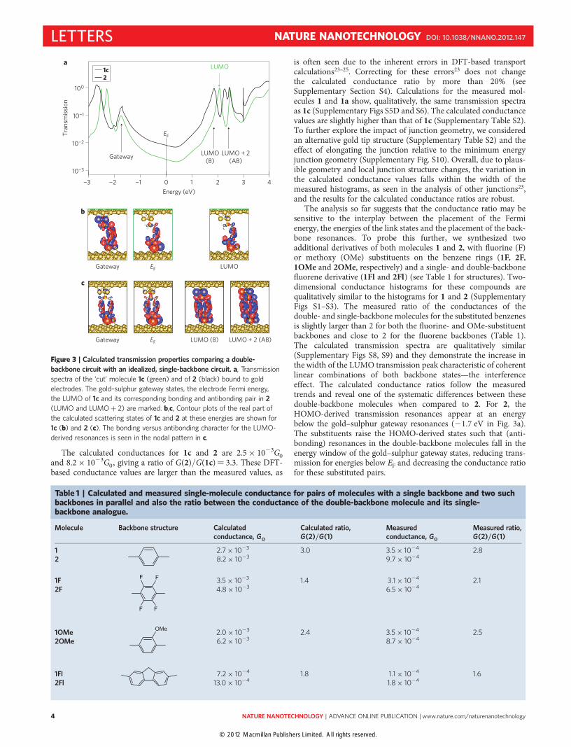
Extensive density functional theory (DFT) studies of junctiontransmission (see Methods and Supplementary Section S4) werecarried out for representative structures to elucidate the impact ofa realistic molecule electronic structure on interference character-istics. To eliminate the role of junction structure in a comparisonof 1 and 2, we began with a model compound 1c, obtained bycutting one backbone out of compound 2 and saturating the cutbonds with hydrogen atoms (Supplementary Fig. S5C). The calcu-lated transmission spectra of 1c and 2 are presented in Fig. 3a,and a visualization of the scattering states in the junction at selectedenergies is shown in Fig. 3b,c. In the unoccupied part of the spec-trum, 2 exhibits twice as many peaks as 1c. The LUMO-derivedp-resonance at 2.1 eV for 1c results in a bonding (LUMO at1.9 eV) and an antibonding (LUMOþ 2 at 2.5 eV) combinationin 2. The bonding peak of 2 is 1.8 times broader than the peak of1c, showing the second characteristic signature of interference.Similarly, the LUMOþ 1 derived peak of 1c at 2.5 eV gives rise
to two peaks for 2 (LUMOþ 1 and LUMOþ 3, shown inSupplementary Fig. S7B); the anti-bonding peak at 3 eV shows dis-persive character, as shown in the model (Fig. 1d). On the occupiedside, the single peaks at 21.7 eV in each spectrum do not representbackbone peaks; rather, they arise from the gold–sulphur bonds (thegateway states in the simplified model) and decay across the back-bones (Fig. 3b,c). This peak due to the gateway states is sharperthan suggested by the simple model in Fig. 1d. A detailed analysisof the scattering states over several electronvolts around EF showsthat the character of the states on the gold–sulphur link atomschanges with energy, modulating the coupling to the electrodesand illustrating the complexity of the full electronic structure.
The Fermi energy falls between the gateway state resonance andthe backbone LUMO resonance. The low bias conductance for allmolecules is dominated by one transmission channel. In eachcase, the scattering state at EF responsible for low bias conductance(Fig. 3b,c) clearly shows tunnelling character. The atomic characterof the gold–sulphur link atoms is similar to the gateway resonance,whereas the through-p-bond portion on the backbones exhibits anodal pattern that is approaching that of the LUMO peak, whichis closest to EF. For the double-backbone case, the transmissionchannel is clearly derived only from the bonding combination ofp backbone states, the signature of constructive interference.
Figure 2 | STM break-junction measurements of single-molecule conductance. a, Sample traces showing conductance as a function of relative tip–sample
displacement for molecules 1, 1a and 2 (the structure of 1a is shown in Supplementary Fig. S6). b, Conductance histograms (on a linear scale) representing
data from more than 6,000 traces for each molecule: 1, 1a and 2. Dashed lines indicate Lorentzian fits to the peaks. Inset: same data on a log scale.
c–e, Two-dimensional conductance–displacement histograms for junctions with molecules 1 (c), 1a (d) and 2 (e). The relative tip–substrate displacement is
set to zero where the gold–gold contact ruptures, and data beyond this rupture are plotted here using logarithmic bins along the conductance axis and
linear bins along the displacement axis. f, Conductance profile determined from two-dimensional histograms for 1, 1a and 2 over a width of 0.1 nm centred at
the end of the low-conductance feature (�0.5 nm displacement) and shown by the vertical lines in c,d and e, respectively. Dashed lines indicate Gaussian
The calculated conductances for 1c and 2 are 2.5 × 10²³G0and 8.2 × 10²³G0, giving a ratio of G(2)/G(1c)¼ 3.3. These DFT-based conductance values are larger than the measured values, as
is often seen due to the inherent errors in DFT-based transportcalculations23–25. Correcting for these errors23 does not changethe calculated conductance ratio by more than 20% (seeSupplementary Section S4). Calculations for the measured mol-ecules 1 and 1a show, qualitatively, the same transmission spectraas 1c (Supplementary Figs S5D and S6). The calculated conductancevalues are slightly higher than that of 1c (Supplementary Table S2).To further explore the impact of junction geometry, we consideredan alternative gold tip structure (Supplementary Table S2) and theeffect of elongating the junction relative to the minimum energyjunction geometry (Supplementary Fig. S10). Overall, due to plaus-ible geometry and local junction structure changes, the variation inthe calculated conductance values falls within the width of themeasured histograms, as seen in the analysis of other junctions23,and the results for the calculated conductance ratios are robust.
The analysis so far suggests that the conductance ratio may besensitive to the interplay between the placement of the Fermienergy, the energies of the link states and the placement of the back-bone resonances. To probe this further, we synthesized twoadditional derivatives of both molecules 1 and 2, with fluorine (F)or methoxy (OMe) substituents on the benzene rings (1F, 2F,1OMe and 2OMe, respectively) and a single- and double-backbonefluorene derivative (1Fl and 2Fl) (see Table 1 for structures). Two-dimensional conductance histograms for these compounds arequalitatively similar to the histograms for 1 and 2 (SupplementaryFigs S1–S3). The measured ratio of the conductances of thedouble- and single-backbone molecules for the substituted benzenesis slightly larger than 2 for both the fluorine- and OMe-substituentbackbones and close to 2 for the fluorene backbones (Table 1).The calculated transmission spectra are qualitatively similar(Supplementary Figs S8, S9) and they demonstrate the increase inthe width of the LUMO transmission peak characteristic of coherentlinear combinations of both backbone states—the interferenceeffect. The calculated conductance ratios follow the measuredtrends and reveal one of the systematic differences between thesedouble-backbone molecules when compared to 2. For 2, theHOMO-derived transmission resonances appear at an energybelow the gold–sulphur gateway resonances (21.7 eV in Fig. 3a).The substituents raise the HOMO-derived states such that (anti-bonding) resonances in the double-backbone molecules fall in theenergy window of the gold–sulphur gateway states, reducing trans-mission for energies below EF and decreasing the conductance ratiofor these substituted pairs.
100
10−1
10−2
10−3
−3 −2 −1 0 21 3 4Energy (eV)
Gateway
EF
LUMO(B)
LUMO + 2(AB)
LUMO1c2
Tran
smis
sion
Gateway EF
Gateway EF
LUMO
LUMO (B) LUMO + 2 (AB)
a
b
c
Figure 3 | Calculated transmission properties comparing a double-
backbone circuit with an idealized, single-backbone circuit. a, Transmission
spectra of the ‘cut’ molecule 1c (green) and of 2 (black) bound to gold
electrodes. The gold–sulphur gateway states, the electrode Fermi energy,
the LUMO of 1c and its corresponding bonding and antibonding pair in 2
(LUMO and LUMOþ 2) are marked. b,c, Contour plots of the real part of
the calculated scattering states of 1c and 2 at these energies are shown for
1c (b) and 2 (c). The bonding versus antibonding character for the LUMO-
derived resonances is seen in the nodal pattern in c.
Table 1 | Calculated and measured single-molecule conductance for pairs of molecules with a single backbone and two suchbackbones in parallel and also the ratio between the conductance of the double-backbone molecule and its single-backbone analogue.
In summary, we have probed the conductance superpositionlaw in single-molecule junctions by combining chemical syn-thesis, single-molecule measurements and transport calculations.Constructive quantum interference in molecules with two parallelbackbones is observed to lead to a characteristic conductance thatis more than twice that of a molecule with a single backbone.Transport calculations also show a characteristic broadening ofthe primary transmission resonances for the double-backbonecase and indicate that the electronic structure of the linker groupplays a subtle but important quantitative role in determining theconductance value. Our experiments and calculations illustratesome of the complexity involved in teasing out clear signatures ofinterference effects in single-molecule junctions.
MethodsExperiments. Single-molecule junctions were created by repeatedly formingand breaking a gold point contact in a solution of the target molecules in1,2,4-trichlorobenzene under 350 mV bias with a velocity of 15 nm s21 in ahome-built STM26. Thousands of traces were collected and presented asconductance histograms, with the peaks corresponding to the most frequentlyobserved conductance values. A freshly cut gold wire (diameter, 0.25 mm; 99.999%purity, Alfa Aesar) was used as the tip, and an ultraviolet/ozone-cleaned goldsubstrate (mica with 100 nm gold, 99.999% purity, Alfa Aesar) was used as thesubstrate. The STM operated under ambient conditions at room temperature. Toensure that each measurement started from a different initial atomic configuration ofthe electrodes, the electrodes were pulled apart only after being brought into contactwith the gold surface, indicated by a conductance greater than a few G0. Beforeadding a molecular solution between the tip and substrate, 1,000 conductance traceswere first collected without molecules to ensure that there were no contaminations inthe STM set-up. Further details are provided in Supplementary Section S3.
Calculations. DFT-based first-principles calculations of electronic transmission27,28
were carried out with a gradient-corrected exchange-correlation functional29 anda non-equilibrium Green’s function approach. Junction structures all correspondedto local energy minima. The real part of the scattering states, calculated forsurface k¼ 0, were presented for analysis30. Further details are presented inSupplementary Section S4.
Received 16 May 2012; accepted 27 July 2012;published online 2 September 2012
References1. Beenakker, C. W. J. & van Houten, H. Quantum transport in semiconductor
nanostructures. Solid State Phys. 44, 1–228 (1991).2. Aharonov, Y. & Bohm, D. Significance of electromagnetic potentials in the
quantum theory. Phys. Rev. 115, 485–491 (1959).3. Webb, R. A., Washburn, S., Umbach, C. P. & Laibowitz, R. B. Observation of h/e
Aharonov–Bohm oscillations in normal-metal rings. Phys. Rev. Lett. 54,2696–2699 (1985).
4. Sautet, P. & Joachim, C. Electronic interference produced by a benzeneembedded in a polyacetylene chain. Chem. Phys. Lett. 153, 511–516 (1988).
5. Patoux, C., Coudret, C., Launay, J-P., Joachim, C. & Gourdon, A. Topologicaleffects on intramolecular electron transfer via quantum interference. Inorg.Chem. 36, 5037–5049 (1997).
6. Mayor, M. et al. Electric current through a molecular rod—relevance of theposition of the anchor groups. Angew. Chem. Int. Ed. 42, 5834–5838 (2003).
7. Kiguchi, M., Nakamura, H., Takahashi, Y., Takahashi, T. & Ohto, T. Effectof anchoring group position on formation and conductance of a singledisubstituted benzene molecule bridging Au electrodes: change of conductivemolecular orbital and electron pathway. J. Phys. Chem. C 114,22254–22261 (2010).
8. Fracasso, D., Valkenier, H., Hummelen, J. C., Solomon, G. C. & Chiechi, R. C.Evidence for quantum interference in SAMs of arylethynylene thiolates intunneling junctions with eutectic Ga–In (EGaIn) top-contacts. J. Am. Chem. Soc.133, 9556–9563 (2011).
9. Guedon, C. M. et al. Observation of quantum interference in molecular chargetransport. Nature Nanotech. 7, 305–309 (2012).
10. Aradhya, S. V. et al. Dissecting contact mechanics from quantum interferencein single-molecule junctions of stilbene derivatives. Nano Lett. 12,1643–1647 (2012).
11. Yaliraki, S. N. & Ratner, M. A. Molecule–interface coupling effects on electronictransport in molecular wires. J. Chem. Phys. 109, 5036–5043 (1998).
12. Magoga, M. & Joachim, C. Conductance of molecular wires connected orbonded in parallel. Phys. Rev. B 59, 16011–16021 (1999).
13. Lang, N. D. & Avouris, P. Electrical conductance of parallel atomic wires. Phys.Rev. B 62, 7325–7329 (2000).
14. Liu, R., Ke, S-H., Baranger, H. U. & Yang, W. Intermolecular effect in molecularelectronics. J. Chem. Phys. 122, 044703 (2005).
15. Landau, A., Kronik, L. & Nitzan, A. Cooperative effects in molecular conduction.J. Comput. Theor. Nanosci. 5, 535–544 (2008).
16. Reuter, M. G., Seideman, T. & Ratner, M. A. Molecular conduction throughadlayers: cooperative effects can help or hamper electron transport. Nano Lett.11, 4693–4696 (2011).
17. Park, Y. S. et al. Contact chemistry and single-molecule conductance: acomparison of phosphines, methyl sulfides, and amines. J. Am. Chem. Soc. 129,15768–15769 (2007).
18. Park, Y. S. et al. Frustrated rotations in single-molecule junctions. J. Am. Chem.Soc. 131, 10820–10821 (2009).
19. Xu, B. Q. & Tao, N. J. Measurement of single-molecule resistance by repeatedformation of molecular junctions. Science 301, 1221–1223 (2003).
20. Quek, S. Y. et al. Mechanically controlled binary conductance switching of asingle-molecule junction. Nature Nanotech. 4, 230–234 (2009).
21. Kamenetska, M. et al. Conductance and geometry of pyridine-linked single-molecule junctions. J. Am. Chem. Soc. 132, 6817–6821 (2010).
22. Martin, C. A. et al. Fullerene-based anchoring groups for molecular electronics.J. Am. Chem. Soc. 130, 13198–13199 (2008).
23. Quek, S. Y. et al. Amine-gold linked single-molecule circuits: experiment andtheory. Nano Lett. 7, 3477–3482 (2007).
24. Quek, S. Y., Choi, H. J., Louie, S. G. & Neaton, J. B. Length dependenceof conductance in aromatic single-molecule junctions. Nano Lett. 9,3949–3953 (2009).
25. Strange, M., Rostgaard, C., Hakkinen, H. & Thygesen, K. S. Self-consistent GWcalculations of electronic transport in thiol- and amine-linked molecularjunctions. Phys. Rev. B 83, 115108 (2011).
26. Venkataraman, L. et al. Single-molecule circuits with well-defined molecularconductance. Nano Lett. 6, 458–462 (2006).
27. Soler, J. M. et al. The SIESTA method for ab initio order-N materials simulation.J. Phys. Condens. Matter 14, 2745–2779 (2002).
28. Brandbyge, M., Mozos, J. L., Ordejon, P., Taylor, J. & Stokbro, K. Density-functional method for nonequilibrium electron transport. Phys. Rev. B 65,165401 (2002).
29. Perdew, J. P., Burke, K. & Ernzerhof, M. Generalized gradient approximationmade simple. Phys. Rev. Lett. 77, 3865–3868 (1996).
30. Paulsson, M. & Brandbyge, M. Transmission eigenchannels fromnonequilibrium Green’s functions. Phys. Rev. B 76, 115117 (2007).
AcknowledgementsThis work was supported primarily by the Nanoscale Science and Engineering Initiative ofthe National Science Foundation (NSF, CHE-0641523), the New York State Office ofScience, Technology, and Academic Research (NYSTAR) and an NSF Career Award to L.V.(CHE-07-44185). L.V. also thanks the Packard Foundation for support. This work wascarried out in part at the Center for Functional Nanomaterials, Brookhaven NationalLaboratory, which is supported by the US Department of Energy, Office of Basic EnergySciences (contract no. DE-AC02-98CH10886). R.S. acknowledges financial support fromthe Canadian postdoctoral fellowship FQRNT programme. S.T.S. acknowledges supportfrom an Arun Guthikonda Memorial graduate fellowship. The authors thank the NSF(CHE-0619638) for the acquisition of an X-ray diffractometer, and G. Parkin and W. Sattlerfor obtaining our crystal structures.
Author contributionsThe experiments were conceived by R.S., S.S., M.K., R.B. and L.V. Theory and calculationswere conceived by H.V. and M.S.H. Synthesis and chemical analysis were performed by R.S.and S.S. Conductance measurements and analysis were performed by M.K and L.V.Calculations were performed by H.V. The manuscript was written by H.V., L.V. and M.S.H.,with comments and input from all other authors.
Additional informationSupplementary information is available in the online version of the paper. Reprints andpermission information is available online at http://www.nature.com/reprints. Correspondenceand requests for materials should be addressed to R.B., L.V. and M.S.H.
Competing financial interestsThe authors declare no competing financial interests.