Probing Topological Magnetism with Transmission Electron Microscopy A Dissertation Presented by Shawn Pollard to The Graduate School in Partial Fulfillment of the Requirements for the Degree of Doctor of Philosophy in Physics Stony Brook University August 2015
Transcript
Probing Topological Magnetism with Transmission Electron Microscopy
A Dissertation Presented
by
Shawn Pollard
to
The Graduate School
in Partial Fulfillment of the
Requirements
for the Degree of
Doctor of Philosophy
in
Physics
Stony Brook University
August 2015
ii
Stony Brook University
The Graduate School
Shawn Pollard
We, the dissertation committee for the above candidate for the
Doctor of Philosophy degree, hereby recommend
acceptance of this dissertation.
Yimei Zhu – Dissertation Advisor
Senior Scientist, CMPMSD, Brookhaven National Laboratory
Adjunct Professor, Department of Physics and Astronomy
Matthew Dawber - Chairperson of Defense
Associate Professor, Department of Physics and Astronomy
Alan Calder
Associate Professor, Department of Physics and Astronomy
Elio Vescovo
Physicist, NSLS-II, Brookhaven National Laboratory
This dissertation is accepted by the Graduate School
Charles Taber
Dean of the Graduate School
iii
Abstract of the Dissertation
Understanding Ordering and Dynamics of Topological Magnetism with Transmission
Electron Microscopy
by
Shawn Pollard
Doctor of Philosophy
in
Physics
Stony Brook University
2015
With recent advances in phase imaging techniques and the development of new, novel specimen
holders in which a variety of stimuli can be applied to magnetic samples in situ, the transmission
electron microscope (TEM) has become a useful tool in studying the properties of magnetic
materials at nanoscale. The resolution afforded by electron microscopy techniques allows for
subtle changes to spin textures to be observed. Here, work on understanding the dynamic
motion of spin-torque and magnetic field driven resonant vortex motion is presented, as well as
experiments in regards to the role of defects in the ordering processes of artificial spin ices.
First, the role that defects and charge ordering play in the ordering processes in artificial spin ice
lattices will be discussed. Experimentally, we find that reversal along the (11) symmetry axis
results in local ground state ordering but long range frustration. Furthermore, defect interactions
ultimately limit their maximum density within the lattice.
Next, while essential to understanding current driven domain wall motion, non-adiabatic spin-
torque effects are poorly understood. In spin-torque driven magnetic vortices, subtle changes to
the magnitude of the resonant orbits with varying chirality allow for the separation of adiabatic,
non-adiabatic, and Oersted field contributions to the motion, as well as for the direct
measurement of the non-adiabatic parameter with the greatest precision to date. Off-resonance
effects are also probed for the first time. Additionally, despite field-driven dynamics of single
vortices near equilibrium being well understood, far-from-equilibrium and coupled dynamics are
significantly more complex, and due to experimental constraints, poorly understood. The
dynamic response in both interlayer exchange coupled vortices in a stack geometry and direct
exchange coupled vortices in a lateral geometry will be explored, and far-from-equilibrium
results will be presented.
iv
Table of Contents
TABLE OF FIGURES ................................................................................................................ VI
ACKNOWLEDGMENTS ....................................................................................................... VIII
PUBLICATIONS ........................................................................................................................ IX
1.1 Context of current work ................................................................................................... 1 1.2 Outline of this dissertation ............................................................................................... 6
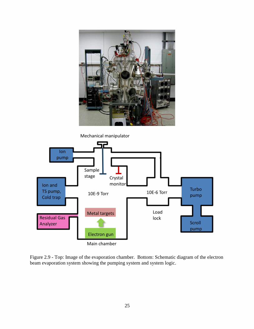
CHAPTER 2. EXPERIMENTAL AND THEORETICAL METHODS .............................. 8
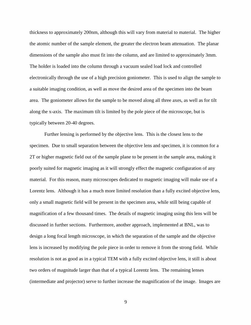
2.1 Basics of TEM .................................................................................................................. 8
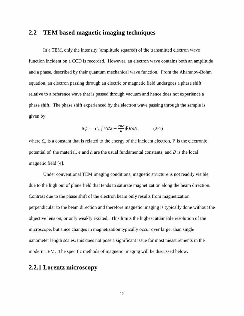
2.2 TEM based magnetic imaging techniques ..................................................................... 12 2.2.1 Lorentz microscopy ................................................................................................ 12
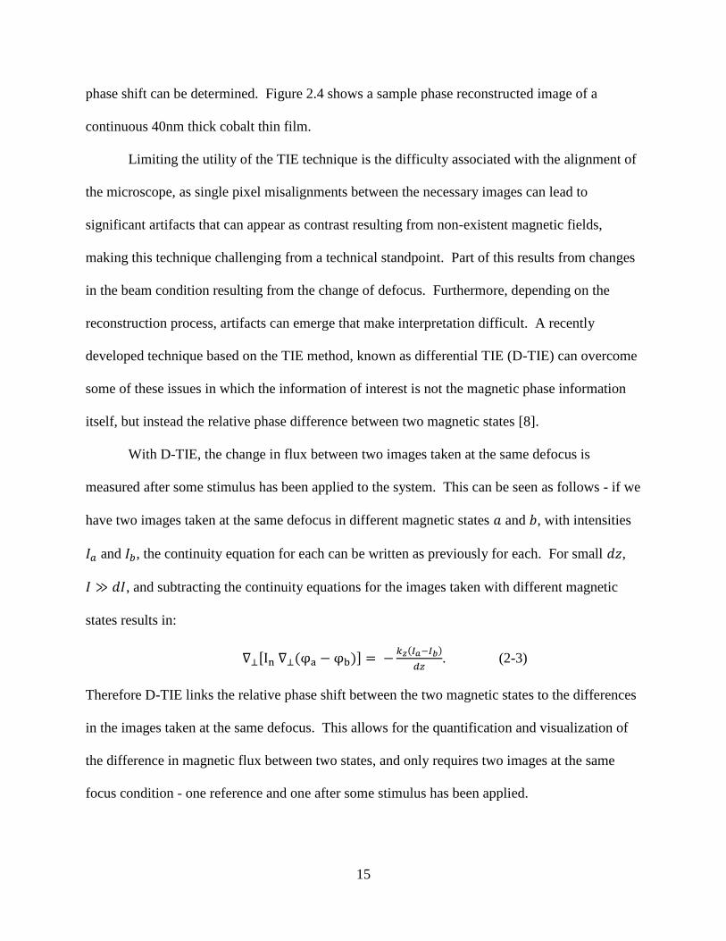
2.2.2 Transport of intensity .............................................................................................. 14
2.2.3 Magnetic imaging with a hole-free carbon phase plate .......................................... 16 2.2.4 Application of magnetic fields and spin excitations in TEM ................................. 19
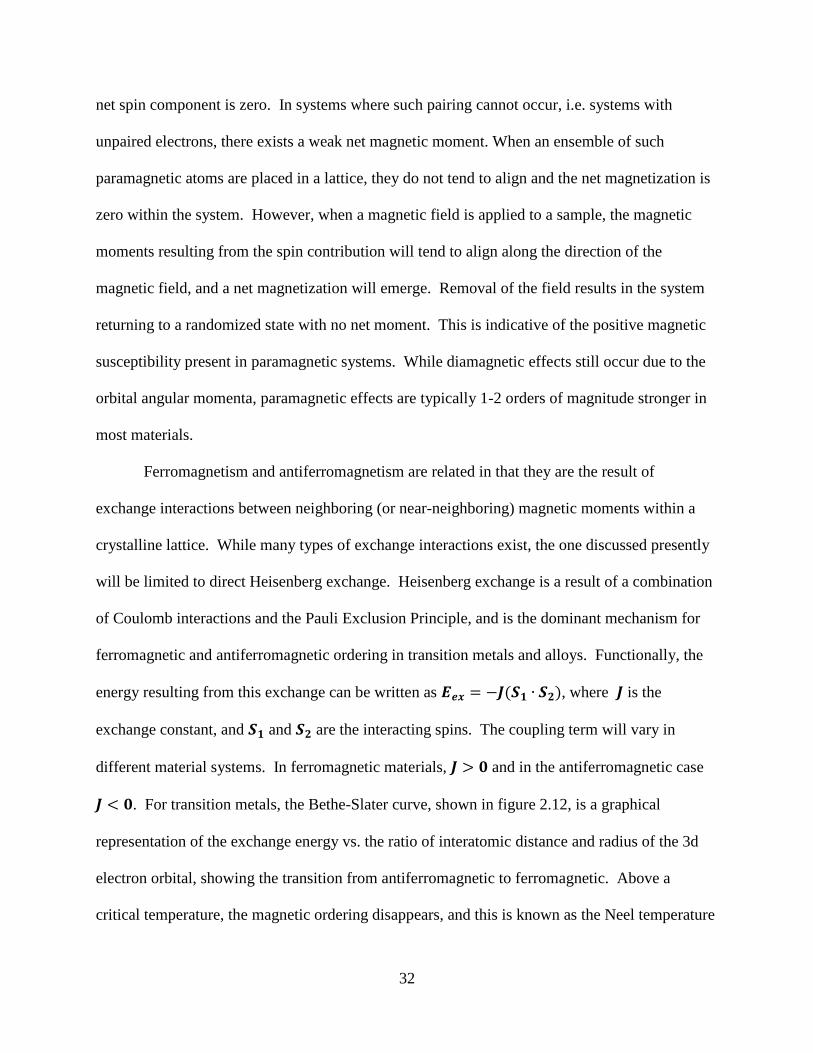
2.5.1 Energies in ferromagnetic materials ....................................................................... 34
2.5.2 The Landau-Lifshitz-Gilbert Equation ......................................................................... 38
2.5.3 Magnetic domains and the role of shape anisotropy ............................................... 40
CHAPTER 3. ORDERING IN ARTIFICIAL SPIN ICE LATTICES .............................. 43
3.1 Introduction to artificial spin ices................................................................................... 43
3.1.1 The magnetic vector potential ................................................................................. 43 3.1.2 The Aharanov-Bohm effect and magnetic monopoles ............................................ 43
3.1.3 Introduction to spin ices .......................................................................................... 47 3.2 Reversal in artificial spin ice lattices.............................................................................. 51
3.2.1 Experimental set-up ................................................................................................ 51 3.2.2 Reversal along the (01)-axis ................................................................................... 55 3.2.3 Reversal along the (11)-axis ................................................................................... 56
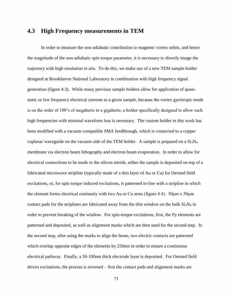
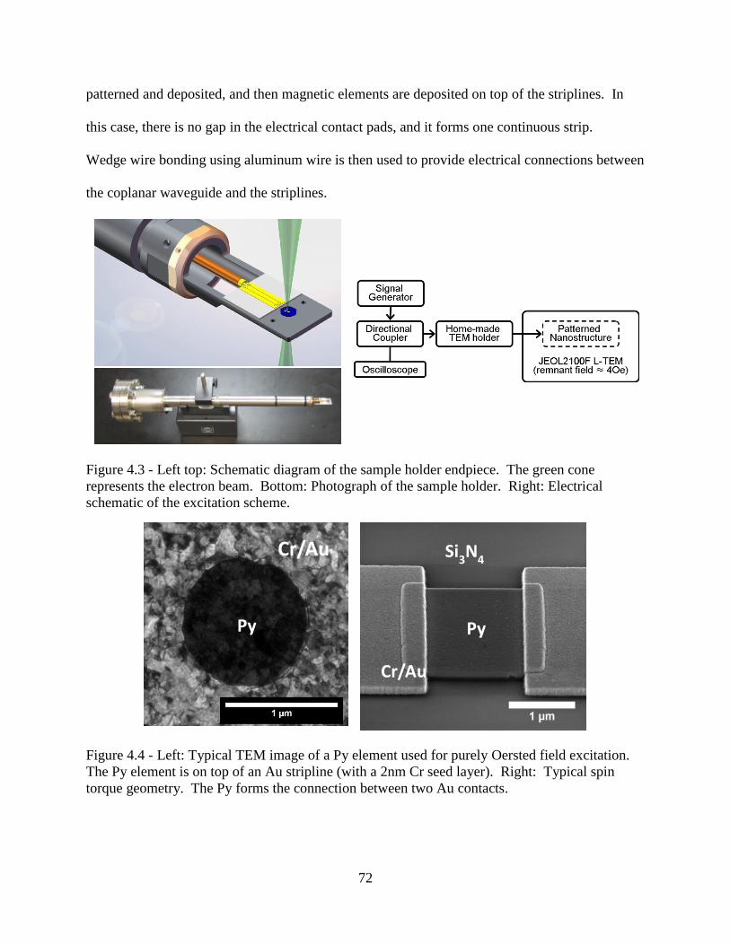
4.2 Introduction to resonant vortex dynamics ...................................................................... 67 4.3 High Frequency measurements in TEM ......................................................................... 71
4.4 General resonance behavior and the determination of 𝜶 ............................................... 73
Figure 4.4 - Left: Typical TEM image of a Py element used for purely Oested field excitation.
The Py element is on top of an Au stripline (with a 2nm Cr seed layer). Right: Typical spin
torque geometry. The Py forms the connection between two Au contacts. ................................. 72
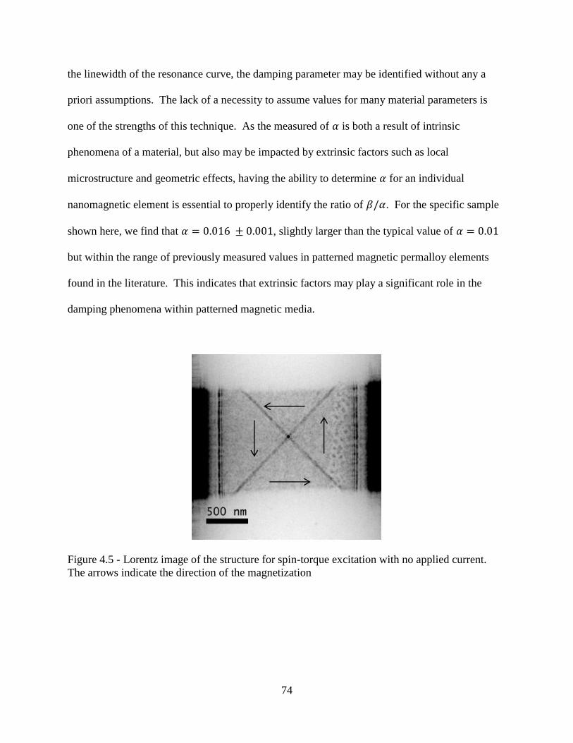
Figure 4.5 - Lorentz image of the structure for spin-torque excitation with no applied current. . 74
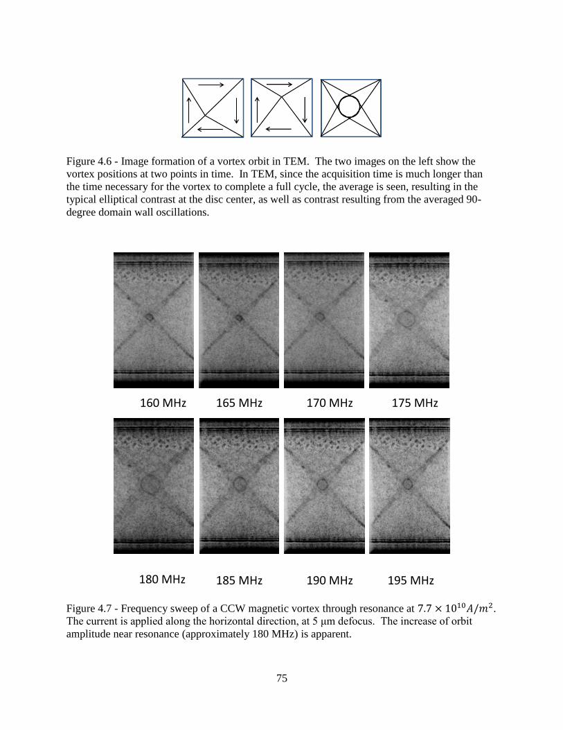
Figure 4.6 - Image formation of a vortex orbit in TEM................................................................ 75
Figure 4.7 - Frequency sweep of a CCW magnetic vortex through resonance at 7.7 ×10¹⁰𝐴/𝑚2. ................................................................................................................................... 75
Figure 4.8 - Resonance curve for the sweep given in Fig. 4.7. ..................................................... 76
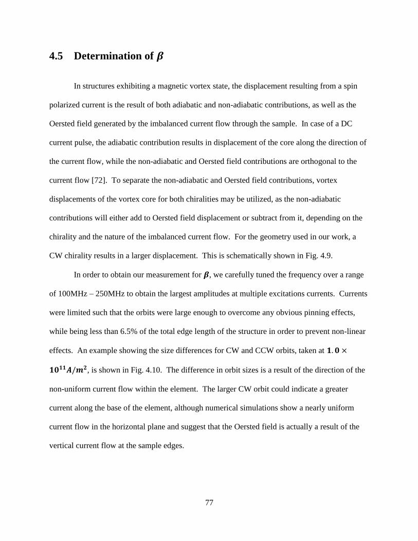
Figure 4.9 - Schematic showing how the three contributions to the vortex displacement add
Figure 4.12 - Ratio of 𝛽 over the full range of possible spin polarizations. A minimum of 𝑃 =0.4 is determined from the literature............................................................................................. 80
Figure 4.13 - Off resonant vortex orbits taken at a current density of 7.9 × 10¹⁰A/m2. .......... 81
Figure 4.14 – Tilt and ellipticity of the vortex orbit vs. frequency taken at 7.9 × 10¹⁰A/m2. .. 82
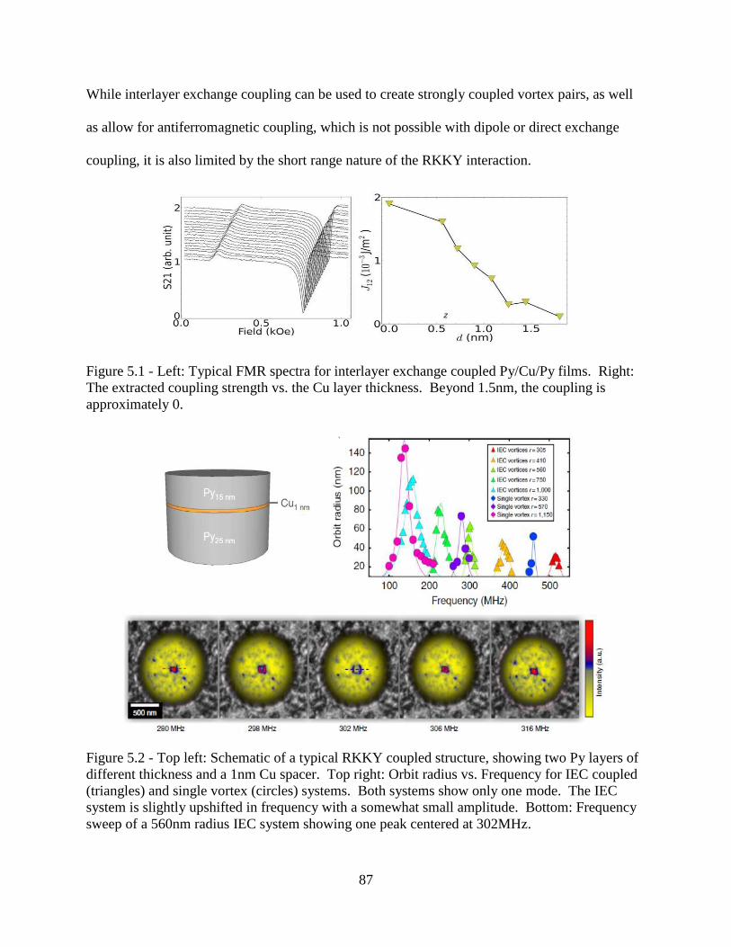
Figure 5.1 – FMR measurements used to determine the RKKY coupling strength in multilayer
In most magnetic systems, the Gibbs free energy can be expressed as the sum of four primary
terms,
𝐸𝑡𝑜𝑡 = 𝐸𝑒𝑥 + 𝐸𝑎𝑛 + 𝐸𝐻 + 𝐸𝑑𝑒𝑚𝑎𝑔, (2-5)
where 𝑬𝒆𝒙 is the total Heisenberg exchange energy, 𝑬𝒂𝒏 is the magneto-crystalline anisotropy
energy, 𝑬𝑯 is the energy resulting from interactions with an externally applied field, and 𝑬𝒅𝒆𝒎𝒂𝒈
is the energy associated with the demagnetizing dipolar interactions. Further energy terms, such
as that which results from the Dzyaloshinkii-Moriya interaction, may be added as necessary, but
typically are small compared to the four energies listed above, and will be ignored in this thesis.
2.5.1 Energies in ferromagnetic materials
35
The Exchange Energy
In ferro- and antiferromagnets, the exchange energy is a result of the strong but short-
range Heisenberg exchange interaction. For two macrospins, 𝑆1 and 𝑆2
, this is typically
expressed as 𝐸𝑒𝑥 = −𝐽(𝑆1 ∙ 𝑆2
), where 𝐽 is the coupling constant and is material specific. The
sign of 𝐽 determines the coupling between neighboring spins. If 𝐽 > 0, parallel spin alignment is
preferred, as is the case in ferromagnetism. If 𝐽 < 0, the coupling is antiferromagnetic. In the
continuum limit, 𝐸𝑒𝑥 may be expressed as
𝐸𝑒𝑥 = 𝐴 ∫ ((∇α)2 +𝑉
(∇β)2 + (∇γ)2)𝑑𝑉, (2-6)
where A is the exchange stiffness constant for the given material, and the integral is taken over
the volume of the magnetic material. When 𝐽 > 0, the energy is minimized if the local
magnetization lies parallel to neighboring magnetic regions.
Magneto-crystalline anisotropy energies
The magneto-crystalline anisotropy energy, 𝐸𝑎𝑛 arises due to coupling between spin and
orbital moments, typically referred to as L-S coupling. Due to this coupling, different crystal
structures will have different preferential magnetization axis depending on their symmetry. The
preferred magnetization axis is known as the crystalline easy axis. For hexagonally closed
packed (hcp) lattices (such as Co), the c-axis represents the easy axis, while it is the <111>- axis
for cubic lattices (such as Ni and Py). Furthermore, the electronic structure plays a vital role in
determining the strength of this anisotropy. For example, for 4f materials, the enhanced L-S
coupling results in strong anisotropies. The energy associated with the magneto-crystalline
anisotropy is usually expressed as a Taylor series. For uniaxial anisotropy, this energy is given
by
36
𝐸𝑎𝑛 = 𝐾1𝑉𝑠𝑖𝑛2𝜃 + 𝐾2𝑉𝑠𝑖𝑛4𝜃 + ⋯, (2-7)
where 𝐸𝑎𝑛 is the anisotropy energy, 𝐾1 and 𝐾2 are the first and second order anisotropy
constants, respectively, 𝑉 is the magnetization volume, and 𝜃 is the angle by which the
magnetization deviates from the crystalline easy axis. For most materials, higher order terms can
be neglected.
Zeeman Energies
The energy from external fields, 𝐸𝐻, is also known as the Zeeman energy. It is a result of
the interactions of a material’s magnetic moments with an externally applied magnetic field, and
is given by
𝐸𝐻 = − ∫ (𝑀 (𝑟 ) ∙ 𝐻 𝑒𝑥(𝑟 ))𝑉
𝑑𝑉, (2-8)
where 𝐻 𝑒𝑥(𝑟 ) is the external magnetic field. This energy is minimized when 𝑀 (𝑟 ) and 𝐻 𝑒𝑥(𝑟 )
lie parallel to one another, and is the reason why a magnet will align along the magnetic field
direction.
Demagnetization Energies
Finally, the demagnetization or dipole energy, 𝐸𝑑𝑒𝑚𝑎𝑔, is the energy resulting from the
interaction of magnetic moments with the magnetic fields resulting from discontinuous
magnetization distributions. This term has contributions from both surface and bulk. The
potential, 𝑈(𝑟 ), related to these contributions is
𝑈(𝑟 ) =1
4𝜋(∫
𝜌(𝑟′ )
|𝑟 −𝑟′ |𝑉𝑑𝑉′ + ∫
𝜎(𝑟′ )
|𝑟 −𝑟′ |𝑆𝑑𝑆′) (2-9)
37
where 𝜌(𝑟 ) = −∇ ∙ 𝑀 (𝑟 ) is the volume charge density and 𝜎(𝑟 ) = 𝑀 (𝑟 ) ∙ 𝑛 is the surface charge
density. From the potential 𝑈(𝑟 ),the demagnetization field 𝐻 𝑑𝑒𝑚𝑎𝑔(𝑟 ) may be derived as
𝐻 𝑑𝑒𝑚𝑎𝑔(𝑟 ) = −∇𝑈(𝑟 ). (2-10)
The demagnetization energy, 𝐸𝑑𝑒𝑚𝑎𝑔, is therefore given by
𝐸𝑑𝑒𝑚𝑎𝑔 = −1
2∫ 𝑀 (𝑟 ) ∙ 𝐻 𝑑𝑒𝑚𝑎𝑔(𝑟 )𝑉
. (2-11)
The dipole energy is long range in nature, and is heavily influenced by the boundary conditions
of a finite structure, and for this reason is sometimes referred to as shape anisotropy energy for
nanostructured materials. From the previously described energy terms, an effective field
experienced by a macrospin may be determined by 𝐻𝑒𝑓𝑓 =𝑑𝐸𝑡𝑜𝑡
𝑑𝑀 𝐸𝑡𝑜𝑡.
Other Energies
It should be noted here that specific energy terms have been omitted as they are not
relevant to the work discussed in this thesis, and only play significant roles in a small subset of
materials or systems. These include indirect exchange energies, which results from RKKY
(Ruderman-Kittel-Kasuya-Yosida) coupling between two ferromagnetic materials separated by a
metallic spacer, and energy resulting from anti-symmetric exchange, present only in certain
materials with strong spin-orbit coupling. In many ferromagnetic patterned structures, it is the
interplay between the demagnetization and exchange energies that lead to the formation of
magnetic domains – the domain structure decreasing the total demagnetization energy, while the
presence of sharp changes in magnetization at domain walls result an increase of the exchange
energy.
38
2.5.2 The Landau-Lifshitz-Gilbert Equation
The Landau-Lifshitz-Gilbert (LLG) equations, initially described by Landau and Lifshitz
in 1935, and modified by Gilbert in 1954 to include a more accurate damping term, is a highly
non-linear ordinary differential equation used to solve the dynamics of macrospins within a bulk
material. Typically, these equations are used to determine possible domain configurations in
micron and submicron sized thin films, observe dynamic properties, or determine resonance
frequencies and spin-wave spectra.
From the standard equation for the torque exerted on a magnetic object with magnetization of
𝑀𝑠 , 𝐿 = −𝑀𝑠
× 𝐻 , where 𝐻 is a magnetic field, and 𝐿 the magnetic torque acting on the body.
Substituting 𝛾𝐿 =𝑑𝑀𝑠
𝑑𝑡 gives the equation for the motion of an undamped macrospin,
𝑑𝑀𝑠
𝑑𝑡=
−𝛾𝑀𝑠 × 𝐻 , where 𝛾 is the gyromagnetic ration. Including a phenomenological damping term,
the full expression for the damped precessional motion of a macrospin influenced by an effective
field may be written as:
𝑑𝑀
𝑑𝑡= −𝛾𝑀 × 𝐻 𝑒𝑓𝑓 +
𝛼
𝑀𝑠𝑀 ×
𝑑𝑀
𝑑𝑡, (2-12)
where 𝛼 is the standard damping constant. The first term describes a precessional motion of 𝑀
about the effective field, while the second term describes the relaxation of 𝑀 towards the
effective field (figure 2.13).
Later, the above model was expanded by Slonczewski to include the effects of spin
transfer torque, by which spin angular momentum carried by electrons within an electric current
could impart angular momentum to a macrospins within a magnetic material and will be
discussed later in this thesis. Most commonly, this equations is solved with the publicly
available software package OOMMF, available from the National Institute of Standards and
39
Technology, in which a given magnetic element is discretized into rectangular cells determined
by the user. For thin films composed of a single material, the thickness is typically neglected,
and the lateral cell sizes should be less than the exchange length of the magnetic material. To
determine a static magnetization distribution, the cells are relaxed iteratively until a convergence
criteria, given by the user, is reached. This is typically set to when 𝑀 × 𝐻 𝑒𝑓𝑓 is below a
specified value. Furthermore, dynamic responses to time varying magnetic fields may also be
simulated. It must be noted that, in cases where the dynamics of the system are important, the
damping parameter plays a key role, and determines how fast and in what manner the
magnetization, when perturbed, relaxes to its new equilibrium state. If the temporal dynamics
are not essential, damping is commonly set to 0.5 or faster so that the system relaxes much more
rapidly, decreasing the total simulation time.
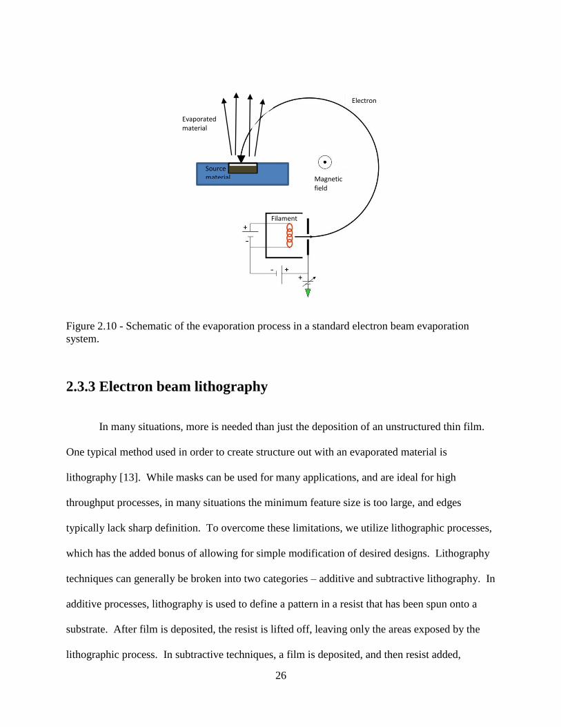
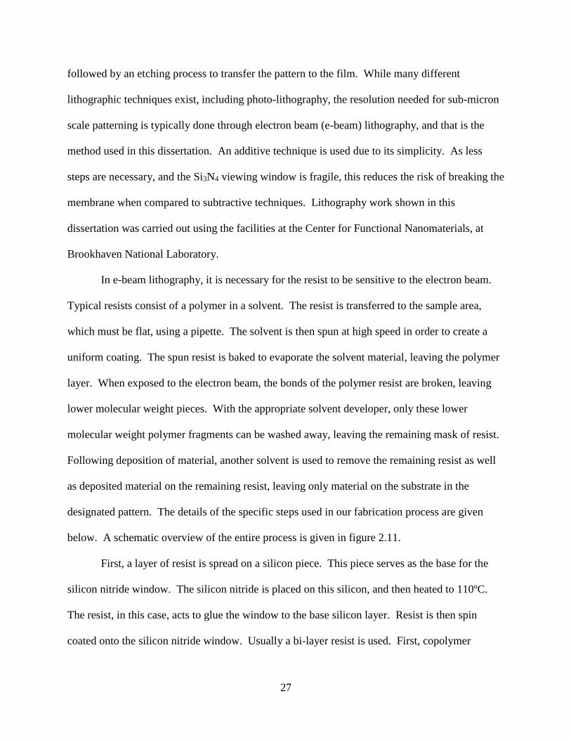
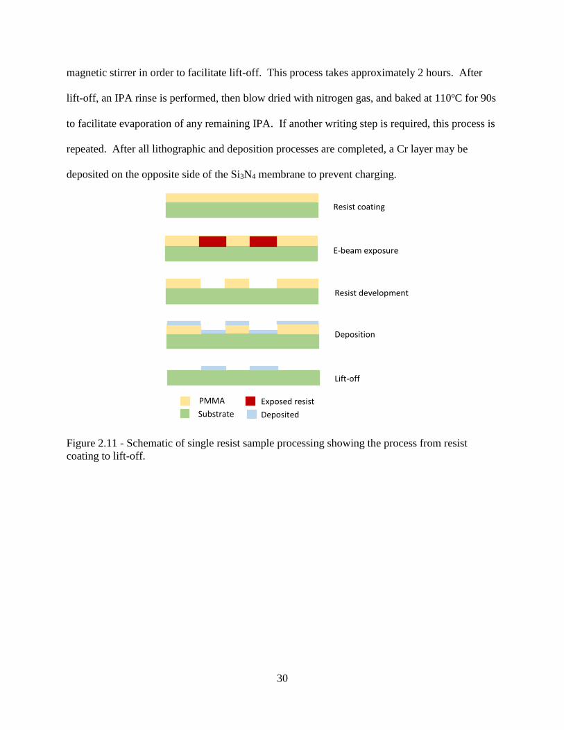
Figure 2.13 - Diagram showing the directions of both the precessional and damping terms in the
LLG equation introduced above. The path of the magnetization is also shown (blue dashed line).
40
2.5.3 Magnetic domains and the role of shape anisotropy
The magnetization distribution of in any magnet is determined via the minimization of
total free energy, which originates from the previously mentioned contributions – exchange,
magneto-crystalline, Zeeman, and demagnetization. The importance of each term depends
heavily on both intrinsic material parameters as well as extrinsic properties such as shape and
externally applied fields. For the majority of the work performed in this thesis, the material of
interest was permalloy (Ni81Fe19), a soft magnetic material with an exchange energy 𝑨 = 𝟏𝟑 ×
𝟏𝟎−𝟏𝟐𝑱/𝒎 and a magnetization saturation of 𝑴𝒔 = 𝟖𝟎𝟎 × 𝟏𝟎𝟑𝑨/𝒎. In this material, a
damping coefficient of 𝜶 = 𝟎. 𝟎𝟏 is typically used, although measurements have shown a range
of values dependent on shape and microstructure of the film. The magneto-crystalline anisotropy
is approximately zero, and can be completely neglected due to the polycrystalline nature of the
films under study.
In general, any large ferromagnetic material at remnance will break into magnetic
domains. These domains are regions within the material in which the magnetic moments lie in
approximately the same direction. For a demagnetized sample, these domains will be randomly
arranged such that the average net magnetization is zero, and is the reason for which many
magnetic materials that are commonly available commercially do no exhibit macroscopic
magnetism. As the dimensions of the magnet shrink, the number of domains present decreases
as well.
At the micron and sub-micron scale, for zero applied field and no magneto-crystalline
anisotropy, the magnetic domain structure is controlled largely via the interplay between
exchange and demagnetization energies. The energetic anisotropies introduced by the shape is
simply known as shape anisotropy. In these thin film structures, the magnetization will lie
41
predominantly in-plane in order to minimize charges on the surface of the film, which would
result in large increases in the demagnetization energy.
Furthermore, in highly symmetric structures such as patterned discs and rectangles, in
order to minimize charges at the edge, will result in the magnetization circulating about a central
point. In the center, the magnetization will cant out-of-plane to avoid generation of a singularity
in which the exchange penalty would be significant. This structure is known as a magnetic
vortex, and the central point is the vortex core. The circulating magnetization can rotate either
clockwise or counterclockwise (CW/CCW) and this is known as the chirality of the vortex, while
the central point can cant either direction perpendicular to the film plane (±1), and this is known
as the polarity (figure 2.14). In other elongated structures, such as nanowires or ellipses with
large aspect ratios, this can result in single domain states where the magnetization points along
the long axis of the element. Single domain magnets may also be generated by decreasing the
element size beyond a critical size limit. In this case, the exchange energy associated with the
creation of a domain wall is prohibitively high, so despite the presence of edge charges, a single
domain structure is maintained. In other shapes, much more complex domain configurations can
be controllably generated via modulations of the physical structure. As the elements increase in
lateral dimensions, multiple domain shapes can be generated. With proper tuning of the in-plane
dimensions of a magnetic thin film, a predefined domain state can be formed in order to further
the understanding of domain dynamics in a controlled fashion.
42
Figure 2.14 - Left: In-plane magnetization of a magnetic vortex structure in a circular disc.
Right. Line scan showing the out-of-plane magnetization in the same disc. The core width is
approximately of 20nm.
43
Chapter 3. Ordering in artificial spin ice lattices
3.1 Introduction to artificial spin ices
3.1.1 The magnetic vector potential
First introduced in the 1800’s by Maxwell, the meaning of magnetic vector potential, 𝐴 ,
and whether it represented a meaningful quantity, was a controversial subject. It was soon
discarded by Heaviside and Hertz as being physically meaningless [14]. However, in the 20th
century vector potentials came in vogue again. Starting with Weyl’s failed attempts to unify
gravity and electromagnetism through the use of a vector potential, eventually Yang and Mills
made use of them in the initial steps towards unifying the nuclear and electromagnetic
forces [15]. In this context, the vector potentials are known as gauge fields, and are now viewed
as fundamental in a variety of settings such as particle and high energy physics. The potential is
related to the phase factor of the electron’s wave function by
exp [−𝑖𝑒
ℏ(∮ 𝐴 𝑑𝑠 − ∮ 𝑉𝑑𝑡)] (3-1)
where 𝑒 is the electron charge, ℏ is the reduced Plank constant, 𝐴 is the vector potential, and 𝑉 is
the scalar potential. The Aharonov-Bohm effect, described in the next section, offers the first
and most complete experimental evidence of the theory of gauge fields.
3.1.2 The Aharanov-Bohm effect and magnetic monopoles
44
The ability to directly measure and image the magnetic and electronic structure of materials in
real space has proven to be invaluable in understanding the fundamental properties of a variety
of systems, ranging from ferromagnets and ferroelectrics to superconductors [16]. In electron
microscopy, a variety of phase imaging techniques exist, ranging from the less quantitative
Fresnel mode [17], to more quantitative methods such as electron holography and the transport-
of-intensity approach [18]. At the root of all of these methods lies the Aharanov-Bohm (AB)
effect, a counterintuitive and fundamentally quantum mechanical phenomenon [4,19]. It is well
known that an electron wave passing through a sample acquires a phase shift. The phase shift is
given by
𝜑 = 𝐶𝑒𝑉𝑡 −𝑒
ℏ∮ 𝐴 𝑑𝑠 , (3-2)
where 𝐶𝑒 is a constant determined by the accelerating voltage of the electron beam, V is the
average potential across the specimen thickness, t is the thickness, and 𝐴 is the vector
potential [16]. Of note, this is the same as the phase factor described in Yang and Mills gauge
theories, and is also the same used in electron interference experiments such as holography.
Commonly, the second term is written in regards to the magnetic field,𝐵 , as
𝜑 = 𝐶𝑒𝑉𝑡 −𝑒
ℏ∫ 𝐵 𝑑𝑆 . (3-3)
However, this form of the equation disregards a fact realized by the individuals for which
the effect is named. In space where 𝐵 = 0, 𝐴 may still have a nonzero value and result in a
phase shift of an electron, which can then be measured via an interference experiment. The
typical description of such an experiment consists of an electron source, a detector, and, in-
between, a solenoidal field that is shielded from the electron wave-front. In theory, the solenoid
should be infinite to eliminate the leakage field, however this is difficult to achieve in
practice [20]. Contrary to intuition, the electrons can experience a phase shift despite
45
experiencing no magnetic field, and, if real, the detector should record an interference pattern
(Fig. 3.1a). Whether this effect was purely mathematical or if it was corresponding to a
physically observable phenomena was heavily debated for many years [21–23], and remained
elusive to experimental verification due to difficulties associated with the measurement. The AB
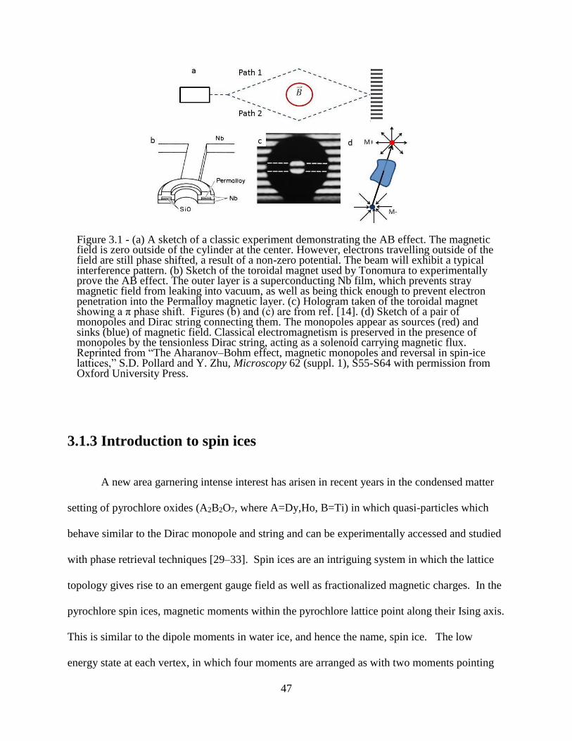
effect was finally proven by Dr. Tonomura in an experimental tour-de-force using a toroidal
permalloy magnet grown on SiO substrate coated by a niobium superconducting film (Fig. 3.1b,
c) [24]. This layer of superconductor not only shielded the toroidal magnet from the incident
electron beam, but the Meissner effect precluded leakage of stray magnetic flux to the
surrounding vacuum. Use of a toroidal magnet also avoided the inherent difficulties in working
with an infinite solenoid, which is experimentally unattainable. While the toroidal magnet itself
was not electron transparent, the beam still passed through vacuum external the toroid and
internally in the circular gap, and the relative phase shift in the gap and external to it could be
measured. In this set-up, the phase shift should be quantized in multiples of π. Electron
interference measured with electron holography showed a clear phase shift of exactly 0 or π. Not
only did this solve a problem in physics that had stood for over 30 years, it also provided
evidence for the theory of gauge fields by demonstrating that the gauge itself, not the magnetic
field, was responsible for the observed phase shift.
Of further importance is the AB effect’s roll in understanding the properties of magnetic
monopoles. Since their prediction by Dirac in 1931 [25,26], the Dirac monopole and Dirac
string have been sought after by physicists in a variety of settings, from the Relativistic Heavy
Ion Collider at Brookhaven National Laboratory to the Large Hadron Collider, to detectors
meant for monopoles produced not by colliders, but as relics from the early universe [27,28].
This special interest is primarily a result of their relation to the quantization of the electric
46
charge. In Dirac’s formulation, the vector potential is that of a standard monopole charge,
producing a field which is the magnetic equivalent to a Coulomb charge. However, to reconcile
quantum mechanics with electromagnetism, Dirac added a line singularity, the Dirac string,
carrying a flux 4πm opposite the monopole flux, preserving ∇ ∙ 𝐵 = 0 (Fig. 3.1d). Gauge
invariance of the string under rotations then implies that 𝑚 =ℏ𝑐
2|𝑒|, where 𝑚 is the magnetic
charge, and 𝑒 is the electron charge. This implies that if a Dirac monopole were to be found, it
would imply the quantization of the electric charge. As we know, electric charges are indeed
quantized. However, despite the intense interest, to this date all studies related to high energy or
particle physics have given a null result with no evidence for a fundamental magnetic charge.
At first glance, the AB effect seems like a useful technique to observe monopole charges
and Dirac strings. While the monopole itself would be observable to the AB effect and give the
correct flux distribution, the Dirac string itself is invisible. By noting that 𝜑 =𝑒
ℏ𝑐∮ 𝐴 𝑑𝑠 =
𝑒
ℏ𝑐(4𝜋𝑚) = 2𝜋𝑛, with n being an integer, after replacing m using the quantization condition,
because phase differences of multiples of 2π are invisible to the AB effect, and hence the
monopole itself would, in fact, be unobservable.
47
Figure 3.1 - (a) A sketch of a classic experiment demonstrating the AB effect. The magnetic field is zero outside of the cylinder at the center. However, electrons travelling outside of the field are still phase shifted, a result of a non-zero potential. The beam will exhibit a typical interference pattern. (b) Sketch of the toroidal magnet used by Tonomura to experimentally prove the AB effect. The outer layer is a superconducting Nb film, which prevents stray magnetic field from leaking into vacuum, as well as being thick enough to prevent electron penetration into the Permalloy magnetic layer. (c) Hologram taken of the toroidal magnet showing a π phase shift. Figures (b) and (c) are from ref. [14]. (d) Sketch of a pair of monopoles and Dirac string connecting them. The monopoles appear as sources (red) and sinks (blue) of magnetic field. Classical electromagnetism is preserved in the presence of monopoles by the tensionless Dirac string, acting as a solenoid carrying magnetic flux. Reprinted from “The Aharanov–Bohm effect, magnetic monopoles and reversal in spin-ice lattices,” S.D. Pollard and Y. Zhu, Microscopy 62 (suppl. 1), S55-S64 with permission from Oxford University Press.
3.1.3 Introduction to spin ices
A new area garnering intense interest has arisen in recent years in the condensed matter
setting of pyrochlore oxides (A2B2O7, where A=Dy,Ho, B=Ti) in which quasi-particles which
behave similar to the Dirac monopole and string and can be experimentally accessed and studied
with phase retrieval techniques [29–33]. Spin ices are an intriguing system in which the lattice
topology gives rise to an emergent gauge field as well as fractionalized magnetic charges. In the
pyrochlore spin ices, magnetic moments within the pyrochlore lattice point along their Ising axis.
This is similar to the dipole moments in water ice, and hence the name, spin ice. The low
energy state at each vertex, in which four moments are arranged as with two moments pointing
48
into, and two out of, the vertex (Fig. 3.2a). In such a situation the ice rules are satisfied
(2in/2out). Defects arise when a moment is switched, resulting in 3 moments into one vertex, and
3 out of another, violating the ice rules. These charges are then separated by switching
subsequent adjacent magnetic moments. It was realized by Castelnova, et. al [31] that these
defects would interact via a coulomb-like interaction and furthermore could be separated without
any tension between them, behaving as free charges. In this situation, the defects could behave
similar to the Dirac monopole and Dirac string, and hence, the ice-rule violating vertices have
been termed monopole defects. These predictions were confirmed experimentally in neutron
scattering, muon spin relaxation, and heat capacity measurements in Dy2Ti2O7 and
Ho2Ti2O7 [30,33]. It should be noted that there are key differences between these emergent
monopoles and flux channels and the Dirac monopole and strings proposed by Dirac himself.
The monopoles that arise in spin ices are unquantized, and therefore observable to the Aharonov-
Bohm effect, provided that the initial and final magnetic configurations of the lattice are known
before and after application of some stimulus that leads to defects (i.e. reversal by a magnetic
field) [34]. Despite the divergence between the emergent monopoles in spin-ices and the
fundamental monopole, their existence in condensed matter systems has opened up a new field in
which magnetic charges interacting via coulombic forces can be studied, as well as the behavior
of flux tubes which are reminiscent of the Dirac string.
In atomic spin ices, these studies are limited due to the inability to use direct imaging
techniques due to the need for atomic scale phase imaging techniques. However, a new
approach has recently been implemented – simulating these atomic scale magnetic moments
using micron-scale magnetic islands which act as analogs to the atomic scale spins of true spin
ices [35]. These micron-scaled islands, when placed in either a square or kagome lattice [36],
49
form the basis for artificial spin ices. In these islands, the shape anisotropy leads to the
magnetization lying along their long axis, and effectively behaving as Ising spins. All islands
point into a vertex, with three elements forming the vertex in the kagome lattice, and four in the
square lattice (Fig. 3.2b). The relative ease of the fabrication process has opened up a wide
variety of parameter space, where coupling at vertices can be varied, disorder controlled, or even
the ice rules can be modified (2 in/1 out or 1 in/2 out in Kagome, 2 in/2 out in the square [36–
40]. Great interest has been devoted to the ordering of these systems, either through the use of a
magnetic field or by thermal excitation [40–43]. Additional studies have focused on how the
excitation and subsequent propagation of the macroscopic analogs to atomic scale spin-ice
monopoles effect the ordering, of which real space imaging can give new insights [44–47].
Beginning with a known initial state, it is relatively straightforward to determine the location of
not only the monopole defects, but also to determine the path that they have taken through the
lattice. It is observed that the monopole defects are connected by chains of switched islands,
which act as magnetic flux tubes. These flux tubes are similar in appearance to the solenoid field
within a Dirac string, but macroscopic, observable, and unquantized. This makes electron
microscopy an ideal tool to study these systems, due to both the scale of the islands and the
change in phase of the electron being observable with the AB effect.
50
Figure 3.2 - (a) Schematic of possible magnetic moment configurations of a tetrahedron in the
pyrochlore spin ice. Where the ice rules are satisfied (top left), there is no net moment (grey).
Where the ice rules are violated, a net moment exists, either negative (blue) when 3 moments
point into a vertex (middle), or positive (red) where 3 moments point out of a vertex. These
vertices behave as magnetic monopoles. (b) Possible vertex combinations in a square artificial
spin ice lattice showing four vertex types with different energies. T-I and T-II vertices satisfy the
2-in/2-out ice rules while the two others violate them. Vertex types are labeled in terms of
increasing energy.
51
3.2 Reversal in artificial spin ice lattices
3.2.1 Experimental set-up
To directly observe ice rule violating defects, the associated connective flux channels,
and related ordering during magnetic reversal, we perform an experiment on artificial square spin
ice that is analogous to that performed on the pyrochlore spin ice in the work by Morris, et.
al [33]. In that case, a field was applied along the (001) axis leading to saturation. It is apparent
that in this configuration the ice rules are satisfied, and no monopole type defects are present.
The system is then removed from saturation by decreasing the field, and the energy is minimized
by the creation of monopole-antimonopole defect pairs connected by chains of switched
elements – “Dirac strings (Fig. 3.3a).” We study a 14x14 vertex array of 100 nm wide, 300 nm
long, and 30 nm thick Permalloy islands arranged in a “square” array by saturating the 2d lattice
shown in figure 3.3b along the (11) axis. Following saturation, a field is applied in either the
(01) direction or the (11) direction until the reordering process is complete. In the intermediate
regime, we track the creation and propagation of monopole type defects in real space as they
traverse the lattice. This behavior is what governs the reversal in these highly frustrated lattices.
It must be noted that the analogy between this artificial spin ice and the pyrochlores is
incomplete. The asymmetry in nearest-neighbor and next-nearest neighbor coupling results in a
non-zero string tension. This can only be removed by adding a height offset between the
different axes of the array [48], which is extremely challenging from an experimental standpoint
and to date has not been achieved.
The array considered was created with standard electron beam lithography and
evaporation techniques. Elements were fabricated such that the center to center spacing of
52
neighboring elements along the same axis was 450nm. Studies were performed in-situ using a
JEOL3000F transmission electron microscope as well as dedicated JEOL2100F-LM Lorentz
microscope. To image local moment configurations, we utilize phase retrieval electron
microscopy – both with Lorentz imaging (Fig. 3.4a-c) and differential transport of intensity (D-
TIE, Fig. 3.4d). As monopole type defects and the connecting strings are defined only by their
excitations above the initial ground state, D-TIE represents a unique technique in which these
excitations may be imaged directly, without convolution of extraneous background fields that
complicate the identification of individual defects. These real space imaging techniques further
allowed for vertex fractions, remnant magnetization, and correlations between individual islands
to be quantified throughout the reversal cycle.
We also link our experimental measurements to numerical results in order to obtain
further insights. In the artificial system, various methods have been used to simulate the system
under different situations, most commonly a simple point dipole model [38,49]. In this method,
used in this work, each individual element of the array is modeled as a point dipole with a critical
switching field. The critical switching field is varied from element to element using a random
Gaussian distribution centered at the critical field, which is determined from experiment.
Switching occurs when the critical switching field (𝐻𝑐,𝑖 ) of the i-th element is exceeded by the
sum of the external field plus the dipole fields of all other elements within the array, i.e. 𝐻𝑒𝑥𝑡 +
∑ 𝐻𝑖𝑗 > 𝐻𝑐,𝑖, where 𝐻𝑒𝑥𝑡 is the external magnetic field component along the (x,y) axes of the i-
th element. The summation is performed over dipolar fields from all j-th elements relative to i-th
element of interest, assuming that i j.
The vertices in the square array consist of four types, labeled as TI to TIV, in order of
increasing energy (Fig. 3.2b). TI and TII obey the 2in/2out ice rules with a net vertex charge Q =
53
0, TIII and TIV do not, with Q = ±2 and Q = ±4 respectively, and are energetically unfavorable.
In this geometry, the asymmetric nature of the four elements composing a vertex results in TI
and TII vertices having different energies despite both following the ice rules, which results in
the nonzero string tension. The ground state of this system consists of a tiling of the lattice with
TI vertices, and due to the frustrated nature of such a system, has been difficult to obtain in
experiment but of great interest for studying frustration physics in real space. A variety of
methods have been used to achieve a pseudo-ground state - most commonly AC demagnetization
protocols in which the sample is spun in a decaying AC magnetic field [35,46,49]. Additionally,
thermal ordering processes during growth appear to show promise in achieving a low energy
ground state [40,42]. To reveal the nature of the switching process in the square ice lattice
studied here, the sample was subjected to magnetic fields along its (01) and (11) and symmetry
axes, respectively, by tilting the sample within the magnetic field generated by the JEOL3000F
microscope’s objective lens [12], and the static state after field application was imaged.
54
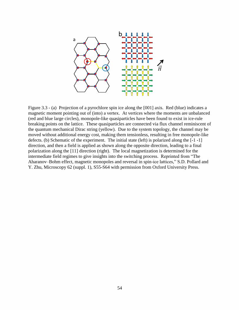
Figure 3.3 - (a) Projection of a pyrochlore spin ice along the [001] axis. Red (blue) indicates a
magnetic moment pointing out of (into) a vertex. At vertices where the moments are unbalanced
(red and blue large circles), monopole-like quasiparticles have been found to exist in ice-rule
breaking points on the lattice. These quasiparticles are connected via flux channel reminiscent of
the quantum mechanical Dirac string (yellow). Due to the system topology, the channel may be
moved without additional energy cost, making them tensionless, resulting in free monopole-like
defects. (b) Schematic of the experiment. The initial state (left) is polarized along the [-1 -1]
direction, and then a field is applied as shown along the opposite direction, leading to a final
polarization along the [11] direction (right). The local magnetization is determined for the
intermediate field regimes to give insights into the switching process. Reprinted from “The
Aharanov–Bohm effect, magnetic monopoles and reversal in spin-ice lattices,” S.D. Pollard and
Y. Zhu, Microscopy 62 (suppl. 1), S55-S64 with permission from Oxford University Press.
b
55
Figure 3.4 - (a) Lorentz TEM image of the square spin ice lattice of the Permalloy specimen.
The arrows indicate the direction of the magnetization of each island. (b) Schematic of two
oppositely magnetized bar elements in Lorentz imaging mode, showing the principle of the
contrast asymmetry of bright(B) and dark(D) depending on the magnetization. (c) Linescan of
the area shown in (a) demonstrating the contrast asymmetry for two oppositely magnetized
elements. This asymmetry (or the location of the white contrast) can be used to determine the
magnetization of each individual element, as marked by the arrows. (d) D-TIE image of the
array, showing only flux associated with the switched elements. The ends of the chains
correspond to the locations of ice rule breaking vertices, with the chains acting as flux channels
between them. Reprinted from “The Aharanov–Bohm effect, magnetic monopoles and reversal
in spin-ice lattices,” S.D. Pollard and Y. Zhu, Microscopy 62 (suppl. 1), S55-S64 with
permission from Oxford University Press.
3.2.2 Reversal along the (01)-axis
When a field was applied along the (01) direction, only elements oriented along that axis
are reversed. Here, the different axes can be viewed as uncoupled. The only effect of the other
axis present is to contribute a position dependent offset to the field required for switching.
Switching occurs through the excitation of a defect pair, which propagates along the applied field
direction. Defects with a charge of -2q (+2q) move opposite (along) the direction of the applied
56
field. In the case of the field being applied along the (01) axis, these chains are limited to the
line of elements in which they nucleated. Nucleation typically, although not always, originates
along edges, where pinning fields from neighboring elements are reduced. Two chains join when
a +2q and a -2q defect come together and annihilate, forming a T-II vertex with no net charge,
and a reduced vertex energy. Low energy T-I vertices and high energy T-IV vertices were never
observed.
3.2.3 Reversal along the (11)-axis
The (11) axis fundamentally differs from the (01) axis due to the nature of its symmetry,
allowing for the formation of low energy vertices which is not possible in the (10) or (01)
reversal. Interactions and correlations between neighboring elements were studied by observing
the in-plane component of the fringing fields of the individual magnetic islands as well as the
local magnetization direction from Lorentz images (Fig. 3.4). This ability to image the field,
unique from other common magnetic imaging techniques such as magnetic force microscopy or
various X-ray techniques, allows for new insights in the physical processes governing to the
frustration to be obtained.
The reversal initiates with the switching of single elements, creating a pair of defects with
opposite charge. As the field is subsequently ramped, these defects propagate through the lattice
in opposite directions, depending on their charge, and leaving behind a tail of switched elements
(Fig. 3.5). These strings act as the channels of magnetic flux between the charges at the ends
(Fig. 3.4d), similar to the solenoidal Dirac string in the classical monopole description. Initially,
there is a marked increase in T-III vertex populations (monopole defects), at the expense of the
57
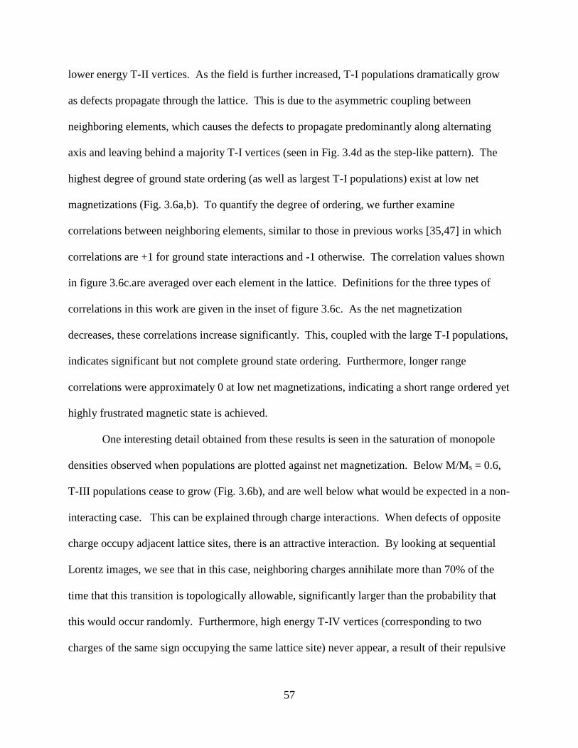
lower energy T-II vertices. As the field is further increased, T-I populations dramatically grow
as defects propagate through the lattice. This is due to the asymmetric coupling between
neighboring elements, which causes the defects to propagate predominantly along alternating
axis and leaving behind a majority T-I vertices (seen in Fig. 3.4d as the step-like pattern). The
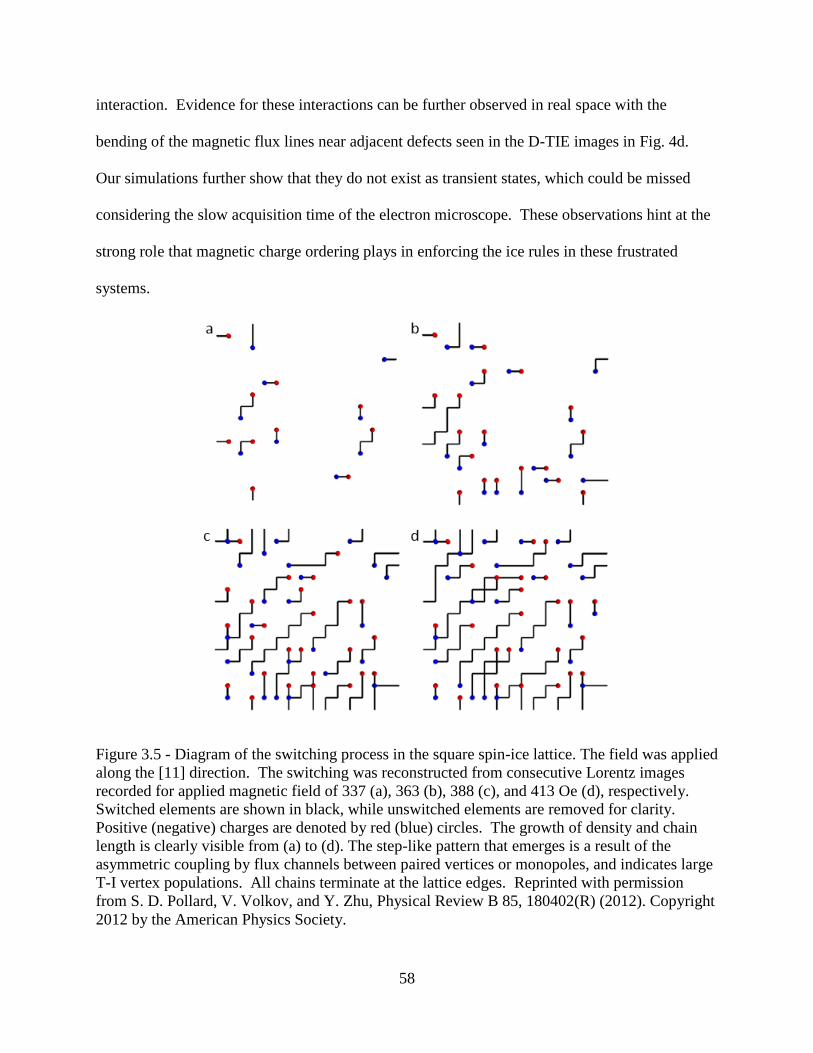
highest degree of ground state ordering (as well as largest T-I populations) exist at low net
magnetizations (Fig. 3.6a,b). To quantify the degree of ordering, we further examine
correlations between neighboring elements, similar to those in previous works [35,47] in which
correlations are +1 for ground state interactions and -1 otherwise. The correlation values shown
in figure 3.6c.are averaged over each element in the lattice. Definitions for the three types of
correlations in this work are given in the inset of figure 3.6c. As the net magnetization
decreases, these correlations increase significantly. This, coupled with the large T-I populations,
indicates significant but not complete ground state ordering. Furthermore, longer range
correlations were approximately 0 at low net magnetizations, indicating a short range ordered yet
highly frustrated magnetic state is achieved.
One interesting detail obtained from these results is seen in the saturation of monopole
densities observed when populations are plotted against net magnetization. Below M/Ms = 0.6,
T-III populations cease to grow (Fig. 3.6b), and are well below what would be expected in a non-
interacting case. This can be explained through charge interactions. When defects of opposite
charge occupy adjacent lattice sites, there is an attractive interaction. By looking at sequential
Lorentz images, we see that in this case, neighboring charges annihilate more than 70% of the
time that this transition is topologically allowable, significantly larger than the probability that
this would occur randomly. Furthermore, high energy T-IV vertices (corresponding to two
charges of the same sign occupying the same lattice site) never appear, a result of their repulsive
58
interaction. Evidence for these interactions can be further observed in real space with the
bending of the magnetic flux lines near adjacent defects seen in the D-TIE images in Fig. 4d.
Our simulations further show that they do not exist as transient states, which could be missed
considering the slow acquisition time of the electron microscope. These observations hint at the
strong role that magnetic charge ordering plays in enforcing the ice rules in these frustrated
systems.
Figure 3.5 - Diagram of the switching process in the square spin-ice lattice. The field was applied
along the [11] direction. The switching was reconstructed from consecutive Lorentz images
recorded for applied magnetic field of 337 (a), 363 (b), 388 (c), and 413 Oe (d), respectively.
Switched elements are shown in black, while unswitched elements are removed for clarity.
Positive (negative) charges are denoted by red (blue) circles. The growth of density and chain
length is clearly visible from (a) to (d). The step-like pattern that emerges is a result of the
asymmetric coupling by flux channels between paired vertices or monopoles, and indicates large
T-I vertex populations. All chains terminate at the lattice edges. Reprinted with permission
from S. D. Pollard, V. Volkov, and Y. Zhu, Physical Review B 85, 180402(R) (2012). Copyright
2012 by the American Physics Society.
59
Figure 3.6 - (a) Vertex populations as a function of applied field. (b) Vertex populations as a
function of normalized net magnetization (M/Ms). Data points are shown for four different
samples during a reversal cycle. In both experimental and numerical results, T-III populations
saturate below a net magnetization of about 0.5. (c) Correlation effects as a function of applied
field. In all plots experimental data are shown by discrete symbols, while theoretical calculations
are shown by solid lines of the appropriate color. Reprinted with permission from S. D. Pollard,
V. Volkov, and Y. Zhu, Physical Review B 85, 180402(R) (2012). Copyright 2012 by the
American Physics Society.
60
3.3 Demagnetization cycling
Due to the high degree of ordering that we have observed during a single reversal cycle
along the (11) axis, comparable to that achieved by a more complicated AC demagnetization
cycle, we use simulations to study how a decaying AC field applied along the (11) axis further
orders the frustrated system. Here we discuss the results of these simulations. Following each
semi-cycle of the hysteresis loop, the maximal field is decreased. The demagnetization using a
(11) cycling is distinctly different from the mechanism that drives the more common AC
demagnetization protocol. Whereas the standard AC demagnetization protocol alternatingly
switches the (10) and (01) axis for different angles during the sample rotation [49], the (11)
cycling simultaneously switches both axis, exploiting the asymmetric coupling of the vertices
along with the symmetry of the (11) axis to achieve local ground state ordering. During
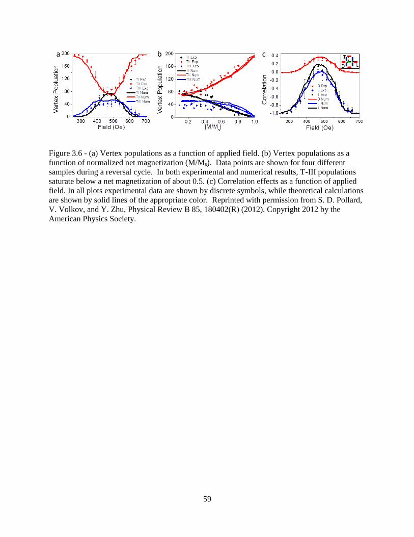
successive cycles, low energy T-I vertices become frozen for subsequent field steps. Meanwhile,
TII vertex links between monopoles can “break”, separating the string into two sets of defect
pairs that then may propagate through the lattice to form more T-I vertices (Fig. 3.7). At the end
of the cycling, the majority of T-III vertices remaining are the results of trapped defects, in which
their motion is only possible through the destruction of a low energy T-I vertex or the creation of
high energy T-IV vertices. This results in the low T-II and T-III populations, while achieving
large populations of T-I vertices as well as large ground state correlations. For the case we
simulated in this work, we used parameters identical to the (11) reversal - a 300Oe switching
field with 60Oe variation with the same misalignment from the (11) axis. The field cycles such
that the maximal amplitude decreases by 20 Oe each half-cycle (Fig. 3.7c). Initial iterations
show no change in correlations of vertex populations from the single cycle reversal, as the
applied field is too large, leaving all T-I vertices unfrozen. However, for intermediate regions,
61
T-I vertices become frozen, and do not change for subsequent cycling. This results in much
larger final T-I populations and correlations at the end of the ordering process as compared to the
simple reversal (Fig, 3.7d, e). Using the (11) AC cycling procedure, we are able to achieve a
near zero net magnetization, along with TI vertex fractions of approximately 62%, with T-III
populations minimized at less than 10% of the total vertex populations. Furthermore,
correlations rise to about 0.60 for D, 0.32 for L, and 0.42 for T, suggesting a high degree of
ground state ordering and a suppression of frustration. This opens up a new method for
achieving a quasi-ground state in which the behavior of emergent monopoles, and their relation
to frustration physics, can be studied on the macroscale.
Figure 3.7 - (a) Definitions for diagonal (D), transverse (T), and Longitudinal (L) correlations in
the square spin-ice lattice. (b) Schematic of the multiple step switching in a (11)
demagnetization. A chain is broken by switching an unfrozen T-II vertex. This creates two new
defects which may propagate, creating new T-I vertices. (c) The demagnetization field cycle
protocol. Each half cycle the field is decreased by 2 mT until it falls below the field required to
switch elements. (d) Vertex population vs. the amplitude of the field for each cycle. (e)
Correlations vs. Field. It is apparent that the end of the cycling results in a high degree of ground
state ordering, but complete ordering is blocked due to frustration effects. Lines in (d) and (c)
correspond to vertex populations and correlations, respectively, at maximal ordering during a
single experimental cycle as reference. Reprinted from “The Aharanov–Bohm effect, magnetic
monopoles and reversal in spin-ice lattices,” S.D. Pollard and Y. Zhu, Microscopy 62 (suppl. 1),
S55-S64 with permission from Oxford University Press.
62
3.4 Summary
In this section, we presented results that give insight into ordering processes in artificial
square spin ice lattices. Specifically, the reversal was tracked using a combination of Lorentz
imaging and D-TIE. This allowed for vertex populations and correlations to be tracked as a
function of field and net magnetization. Short range interactions between defects limit the
overall population of defects within the lattice, as attractive interactions between defects of
opposite charge tend to lead to annihilation of defect pairs for neighboring vertices.
Furthermore, we found that by proper selection of applied field direction, a high degree of local
ground state ordering could be achieved, although long ordering was still blocked due to
frustration effects. With this in mind, we have proposed a simple method in which an even
larger degree of ground state ordering could be achieved, and tested this using a numerical model
based on treating the elements as Ising spins that interact solely through dipole-dipole
interactions.
63
Chapter 4. Spin torque driven magnetic vortex dynamics
4.1 Motivation
In ferromagnets, imbalances between spin populations of conduction electrons result in
the spin polarization of an electrical current that flows through a ferromagnet. This spin
polarized current imparts spin angular momenta, in addition to the charge current, to the local
magnetic moments composing the ferromagnet, and as such can cause changes in the local spin
texture. In the LLG equations, this is accounted for via the introduction of two new
phenomenological terms representing adiabatic and non-adiabatic contributions, respectively.


![Probing topological transitions in HgTe/CdTe quantum wells ... · Since the first theoretical predictions of the quantum spin Hall(QSH)effectingraphene[1,2]andininvertedHgTe/CdTe](https://static.documents.pub/doc/80x56/6004444aa404b8463202aae5/probing-topological-transitions-in-hgtecdte-quantum-wells-since-the-irst.jpg)


