RF-Powered Micromechanical Clock Generator Ruonan Liu, Jalal Naghsh Nilchi, and Clark T.-C. Nguyen Dept. of Electrical Engineering and Computer Sciences University of California at Berkeley Berkeley, California, USA [email protected]Abstract—A micromechanical circuit has been demonstrated that harnesses resonant mechanical impact switching to convert received RF energy (at −58dBm) into a local 1-kHz clock output while consuming less than 17.5nW of local battery power, which is 57 times lower than the 1W of a typical real-time clock (RTC). The principal enabler here is a micromechanical resonant switch ("resoswitch") that first accepts incoming ASK or FSK clock- modulated RF energy at a carrier frequency, filters it to remove unwanted interferers, provides power gain via resonant impact switching, and finally envelop detects impact impulses to demodulate and recover the clock waveform from the carrier. Since the resulting time domain waveform derives from the presumably very stable clock signal that originally modulated the RF carrier, the resulting local clock can share its accuracy. By dispensing with the need for a positive feedback sustaining amplifier, such a 1-kHz RF-powered mechanical clock generator driving an on-chip inverter gate capacitance of 5fF can potentially operate with only 5pW of battery power, which is 200,000 times lower than the typical RTC! Using an off-chip inverter with 17.5pF of effective capacitance, the current laboratory demonstration at 1-kHz consumes a still tiny 17.5nW. Keywords—clock recovery, real-time clock, MEMS, wireless, low power, squegging, time transfer. I. INTRODUCTION The widespread expectation that autonomous sensor networks will fuel massively accessible information technology, such as the Internet of Things (IoT) [1], comes with the daunting realization that huge numbers of sensor nodes will be required, perhaps approaching one trillion. Needless to say, besides cost, energy will likely pose a major constraint in such a vision. If sleep/wake strategies can adequately limit a given node’s sensor and wireless power consumption, the power bottleneck then comes down to the real-time clock (RTC) that synchronizes sleep/wake cycles. With typical RTC battery consumption on the order of 1W, a low-cost printed battery with perhaps 1J of energy would last only 11.5 days. On the other hand, if a clock could bleed only 10nW from this battery, it would last 3 years. Pursuant to attaining such a clock, this work explores a wireless approach that dispenses with the conventional closed- loop positive feedback approach to realizing an RTC (along with its associated power consumption) and removes the need for a sustaining amplifier altogether. Fig. 1 illustrates how such a clocking scheme might work. Here, applications that employ RTC’s—which include virtually every electronic device, from phones, to televisions, to appliances—now no longer house positive feedback oscillator RTC's. Rather, RF receiver circuits replace the clocks, while base stations supply the timing waveform remotely. If the carrier frequency used is sufficiently low, transmitted RF clock signals can penetrate buildings and other structures, even into some tunnels. Existing infrastructure, such as AM or FM radio towers, could broadcast clock signals in addition to their usual content. If frequencies are low enough, e.g., WWVB signals already transmitted by NIST in Colorado, then cross-country transmission is even possible. Of course, receivers for WWVB signals already exist, and unfortunately, they consume 300W of power when on and listening. This is much more than the 1 W of the typical RTC and is obviously why the proposed Fig. 1 clock distribution scheme for everyday electronics is not presently desirable. To fix this problem, this work explores the use of a MEMS- based RF receiver to eliminate quiescent power consumption and greatly reduce the power needed to recover a clock waveform from a suitable RF input. The clock generator specifically employs a micromechanical resoswitch as a filter- LNA combination [2], pictured and summarized in Fig. 2, to first absorb incoming FSK signal energy at its resonance frequency (cf. Fig. 2(c)), block other RF components not at resonance, then convert the FSK waveform to a lower frequency clock waveform (cf. Fig. 2(e)). A final low power inverter then converts the output to a square wave to remove amplitude noise components. Unlike a conventional transistor receiver, this mechanical version consumes no dc power while “listening” for a valid RF clock signal. When it receives the RF clock signal, it then generates the needed clock waveform with considerably less power than otherwise consumed by a positive-feedback RTC Fig. 1: Illustration of a wireless clock vision, where instead of carrying power hungry local clocks based on positive feedback circuits, electronics and appliances receive clock signals remotely via ultra-low power mechanical receivers. As long as their frequencies are low enough, transmitted RF clock carriers can penetrate obstacles and travel over large distances, even cross- country. R. Liu, J. N. Nilchi, and C. T.-C. Nguyen, “RF-powered micromechanical clock generator,” Proceedings, IEEE Int. Frequency Control Symp., New Orleans, Louisiana, May 9-12, 2016, pp. 73-78. (best paper award winner)
Transcript
RF-Powered Micromechanical Clock Generator
Ruonan Liu, Jalal Naghsh Nilchi, and Clark T.-C. Nguyen
Dept. of Electrical Engineering and Computer Sciences
The widespread expectation that autonomous sensor networks will fuel massively accessible information technology, such as the Internet of Things (IoT) [1], comes with the daunting realization that huge numbers of sensor nodes will be required, perhaps approaching one trillion. Needless to say, besides cost, energy will likely pose a major constraint in such a vision. If sleep/wake strategies can adequately limit a given node’s sensor and wireless power consumption, the power bottleneck then comes down to the real-time clock (RTC) that synchronizes sleep/wake cycles. With typical RTC battery consumption on the
order of 1W, a low-cost printed battery with perhaps 1J of energy would last only 11.5 days. On the other hand, if a clock could bleed only 10nW from this battery, it would last 3 years.
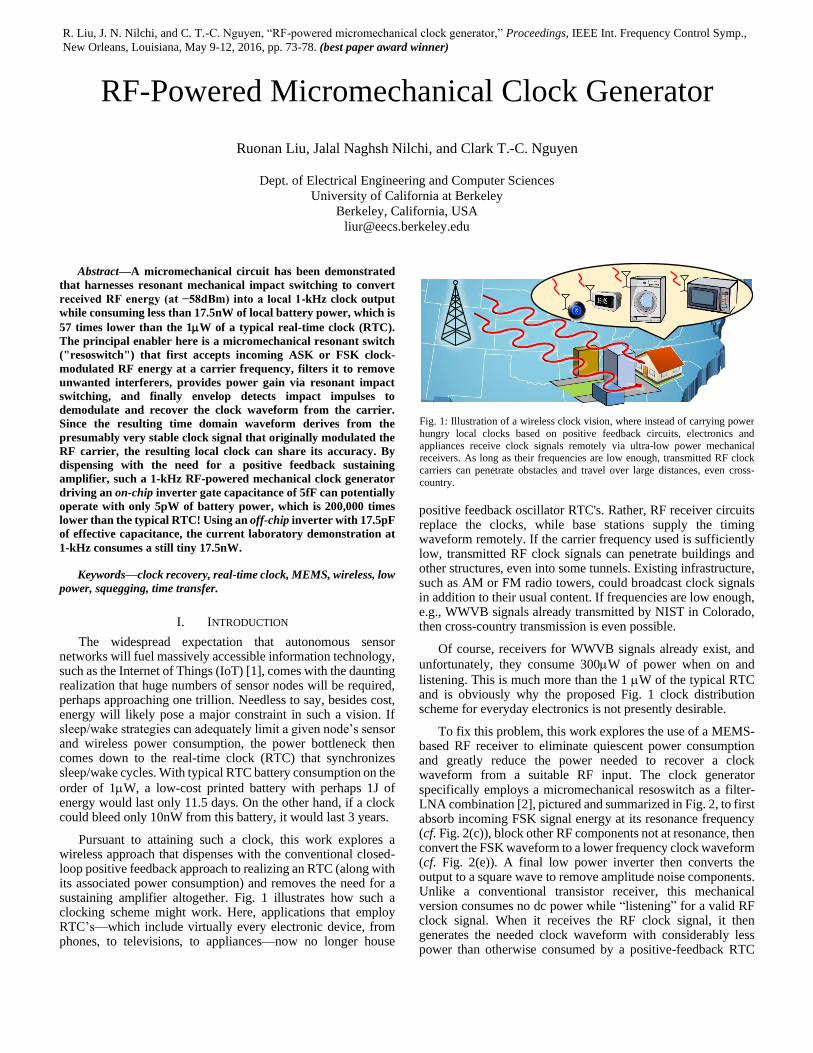
Pursuant to attaining such a clock, this work explores a wireless approach that dispenses with the conventional closed-loop positive feedback approach to realizing an RTC (along with its associated power consumption) and removes the need for a sustaining amplifier altogether. Fig. 1 illustrates how such a clocking scheme might work. Here, applications that employ RTC’s—which include virtually every electronic device, from phones, to televisions, to appliances—now no longer house
positive feedback oscillator RTC's. Rather, RF receiver circuits replace the clocks, while base stations supply the timing waveform remotely. If the carrier frequency used is sufficiently low, transmitted RF clock signals can penetrate buildings and other structures, even into some tunnels. Existing infrastructure, such as AM or FM radio towers, could broadcast clock signals in addition to their usual content. If frequencies are low enough, e.g., WWVB signals already transmitted by NIST in Colorado, then cross-country transmission is even possible.
Of course, receivers for WWVB signals already exist, and
unfortunately, they consume 300W of power when on and
listening. This is much more than the 1 W of the typical RTC and is obviously why the proposed Fig. 1 clock distribution scheme for everyday electronics is not presently desirable.
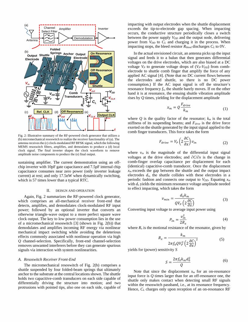
To fix this problem, this work explores the use of a MEMS-based RF receiver to eliminate quiescent power consumption and greatly reduce the power needed to recover a clock waveform from a suitable RF input. The clock generator specifically employs a micromechanical resoswitch as a filter-LNA combination [2], pictured and summarized in Fig. 2, to first absorb incoming FSK signal energy at its resonance frequency (cf. Fig. 2(c)), block other RF components not at resonance, then convert the FSK waveform to a lower frequency clock waveform (cf. Fig. 2(e)). A final low power inverter then converts the output to a square wave to remove amplitude noise components. Unlike a conventional transistor receiver, this mechanical version consumes no dc power while “listening” for a valid RF clock signal. When it receives the RF clock signal, it then generates the needed clock waveform with considerably less power than otherwise consumed by a positive-feedback RTC
Fig. 1: Illustration of a wireless clock vision, where instead of carrying power
hungry local clocks based on positive feedback circuits, electronics and
appliances receive clock signals remotely via ultra-low power mechanical receivers. As long as their frequencies are low enough, transmitted RF clock
carriers can penetrate obstacles and travel over large distances, even cross-
country.
R. Liu, J. N. Nilchi, and C. T.-C. Nguyen, “RF-powered micromechanical clock generator,” Proceedings, IEEE Int. Frequency Control Symp.,
New Orleans, Louisiana, May 9-12, 2016, pp. 73-78. (best paper award winner)
sustaining amplifier. The current demonstration using an off-chip inverter with 10pF gate capacitance and 7.5pF internal chip capacitance consumes near zero power (only inverter leakage current) at rest; and only 17.5nW when dynamically switching, which is 57 times lower than a typical RTC.
II. DEISGN AND OPERATION
Again, Fig. 2 summarizes the RF-powered clock generator, which comprises an all-mechanical receiver front-end that detects, amplifies, and demodulates clock-modulated RF input power; followed by an optional inverter that converts an otherwise triangle-wave output to a more perfect square wave clock output. The key to low power consumption lies in the use of a micromechanical resoswitch [3] (shown in Fig. 2(b)) that demodulates and amplifies incoming RF energy via nonlinear mechanical impact switching while avoiding the deleterious effects commonly associated with nonlinear operation via high Q channel-selection. Specifically, front-end channel-selection removes unwanted interferers before they can generate spurious signals via interaction with system nonlinearities.
A. Resoswitch Receiver Front-End
The micromechanical resoswitch of Fig. 2(b) comprises a shuttle suspended by four folded-beam springs that ultimately anchor to the substrate at the central locations shown. The shuttle holds two capacitive-comb transducers on each side capable of differentially driving the structure into motion; and two protrusions with pointed tips, also one on each side, capable of
impacting with output electrodes when the shuttle displacement exceeds the tip-to-electrode gap spacing. When impacting occurs, the conductive structure periodically closes a switch between the power supply VDD and the output node, delivering power from VDD to CL and charging it in the process. When impacting stops, the bleed resistor Rbleed discharges CL to 0V.
In the actual envisioned circuit, an antenna picks up the input signal and feeds it to a balun that then generates differential voltages on the drive electrodes, which are also biased at a DC voltage VP to generate voltage drops of (VP-VDD) from comb-electrode to shuttle comb finger that amplify the force of any applied AC signal [4]. (Note that no DC current flows between the electrodes and shuttle, so there is no DC power consumption.) If the AC input signal is off the structure’s resonance frequency fo, the shuttle barely moves. If on the other hand it is at resonance, the ensuing shuttle vibration amplitude rises by Q times, yielding for the displacement amplitude
𝑥𝑚 = 𝑄
𝐹𝑑𝑟𝑖𝑣𝑒𝑘𝑚
(1)
where Q is the quality factor of the resonator; km is the total stiffness of its suspending beams; and Fdrive is the drive force exerted on the shuttle generated by the input signal applied to the comb finger transducers. This force takes the form
𝐹𝑑𝑟𝑖𝑣𝑒 = 𝑉𝑃 (2
𝜕𝐶
𝜕𝑥) 𝑣𝑖𝑛 (2)
where vin is the magnitude of the differential input signal
voltages at the drive electrodes; and C/x is the change in comb-finger overlap capacitance per displacement for each (identical) capacitive-comb transducer. Once the displacement xm exceeds the gap between the shuttle and the output impact electrodes do, the shuttle collides with these electrodes in a periodic fashion and connects one output to VDD. Equating xm with do yields the minimum resonance voltage amplitude needed to effect impacting, which takes the form
𝑣𝑚𝑖𝑛 =
𝑑0𝑘𝑚
𝑄𝑉𝑃 (2𝜕𝐶𝜕𝑥) (3)
Converting input voltage to average input power using
𝑃𝑖𝑛 =
𝑣𝑖𝑛2
2𝑅𝑥 (4)
where Rx is the motional resistance of the resonator, given by
𝑅𝑥 =
𝑘𝑚
2𝜋𝑓0𝑄𝑉𝑃2 (2
𝜕𝐶𝜕𝑥)2 (5)
yields for (power) sensitivity S
𝑆 =2𝜋𝑓0𝑘𝑚𝑑0
2
𝑄 (6)
Note that since the displacement xm for an on-resonance input force is Q times larger than for an off-resonance one, the shuttle only makes contact when detecting small RF signals within the resoswitch passband, i.e., at its resonance frequency. Hence, CL charges only upon reception of an on-resonance RF
Fig. 2: Illustrative summary of the RF-powered clock generator that utilizes a (b) micromechanical resoswitch to realize the receiver functionality of (a). The
antenna receives the (c) clock-modulated RF BFSK signal, which the following
MEMS resoswitch filters, amplifies, and demoulates to produce a (d) local clock signal. The final inverter shapes the clock waveform to remove
amplitude noise components to produce the (e) final output.
(a)
(b)
Channel
Select FilterAmplifier
Antenna
Inverter
Demodulation
(b)
On Resonance
Vin
Anchor
VP
VDD
Rb
lee
d
CL
VCLK
Vout VDD
Off Resonance
Shuttle
Output
Electrode
Output
ElectrodeShuttle
Folded
Springs
Comb
Transducers
(e)
VinVout VCLK
tt t
Off Resonance(c) (d)Ref. CLKOutput CLK
input, but otherwise discharges to 0V. So effectively, the resoswitch first channel-select filters the input signal, rejecting practically all out-of-band power; amplifies any in-band signal via impact switching to VDD, sending power from VDD to the output; and charges/discharges capacitor CL according to RF input temporal frequency changes and the bleed rate of Rbleed, all of which amounts to FM demodulation. In effect, we have a filter-LNA-demodulator function in one device.
B. Clock Generator
Given the above description of resoswitch operation, one input scheme (perhaps transmitted by a base station) that generates the desired square-wave clock output is a simple clock-modulated BFSK signal (Fig. 2(c)) that simply hops back-and-forth between an on-resonance mark frequency fmark (representing a '1') and an off-resonance space frequency fspace
(representing a '0') with a period corresponding to the desired clock rate fCLK. Here, each time span at fmark induces impacts and charges CL to VDD; while each at fspace stops impacts, allowing CL to discharge to 0V via bleed resistor Rbleed; all resulting in a square wave with amplitude VDD and period governed by the originally modulating source clock. This means the accuracy of the demodulated (local) clock should be practically the same as that of the source clock, which could be extremely good.
C. Clock Stability
Although the received clock signal can be quite accurate, its stability is subject to numerous events. In particular, if the output signal is taken at the Vout node indicated in Fig. 2(b), then for a given value of bleed resistance Rbleed the output waveform might resemble the sawtooth shown in Fig. 2(d), with fast rise times and slow fall times. Here, consistency of the rising edge of each sawtooth governs to some extent the stability of the local clock.
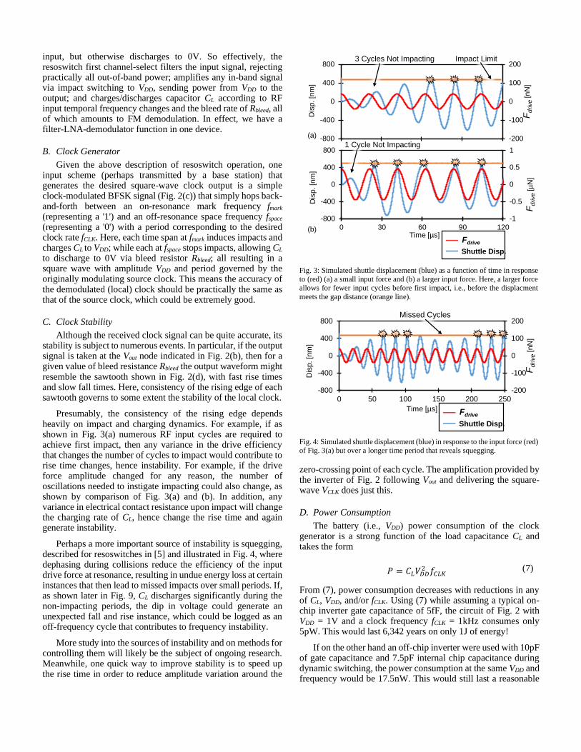
Presumably, the consistency of the rising edge depends heavily on impact and charging dynamics. For example, if as shown in Fig. 3(a) numerous RF input cycles are required to achieve first impact, then any variance in the drive efficiency that changes the number of cycles to impact would contribute to rise time changes, hence instability. For example, if the drive force amplitude changed for any reason, the number of oscillations needed to instigate impacting could also change, as shown by comparison of Fig. 3(a) and (b). In addition, any variance in electrical contact resistance upon impact will change the charging rate of CL, hence change the rise time and again generate instability.
Perhaps a more important source of instability is squegging, described for resoswitches in [5] and illustrated in Fig. 4, where dephasing during collisions reduce the efficiency of the input drive force at resonance, resulting in undue energy loss at certain instances that then lead to missed impacts over small periods. If, as shown later in Fig. 9, CL discharges significantly during the non-impacting periods, the dip in voltage could generate an unexpected fall and rise instance, which could be logged as an off-frequency cycle that contributes to frequency instability.
More study into the sources of instability and on methods for controlling them will likely be the subject of ongoing research. Meanwhile, one quick way to improve stability is to speed up the rise time in order to reduce amplitude variation around the
zero-crossing point of each cycle. The amplification provided by the inverter of Fig. 2 following Vout and delivering the square-wave VCLK does just this.
D. Power Consumption
The battery (i.e., VDD) power consumption of the clock generator is a strong function of the load capacitance CL and takes the form
𝑃 = 𝐶𝐿𝑉𝐷𝐷
2 𝑓𝐶𝐿𝐾 (7)
From (7), power consumption decreases with reductions in any of CL, VDD, and/or fCLK. Using (7) while assuming a typical on-chip inverter gate capacitance of 5fF, the circuit of Fig. 2 with VDD = 1V and a clock frequency fCLK = 1kHz consumes only 5pW. This would last 6,342 years on only 1J of energy!
If on the other hand an off-chip inverter were used with 10pF of gate capacitance and 7.5pF internal chip capacitance during dynamic switching, the power consumption at the same VDD and frequency would be 17.5nW. This would still last a reasonable
Fig. 3: Simulated shuttle displacement (blue) as a function of time in response
to (red) (a) a small input force and (b) a larger input force. Here, a larger force
allows for fewer input cycles before first impact, i.e., before the displacment
meets the gap distance (orange line).
Fig. 4: Simulated shuttle displacement (blue) in response to the input force (red)
of Fig. 3(a) but over a longer time period that reveals squegging.
-200
-100
0
100
200
-800
-400
0
400
800
Fd
rive
[nN
]
Dis
p. [n
m]
-1
-0.5
0
0.5
1
-800
-400
0
400
800
0 30 60 90 120
Fd
rive
[µ
N]
Dis
p. [n
m]
Time [µs]Fdrive
Shuttle Disp.
3 Cycles Not Impacting Impact Limit
(a)
(b)
1 Cycle Not Impacting
-200
-100
0
100
200
-800
-400
0
400
800
0 50 100 150 200 250
Fd
rive
[nN
]
Dis
p. [n
m]
Time [µs] Fdrive
Shuttle Disp.
Missed Cycles
1.8 years on 1J. If the clock frequency were reduced to 1 Hz (for a 1 second period), then only 17.5pW would be needed, and the clock would again last quite long on 1J—1,812 years, to be exact.
III. EXPERIMENTAL RESULTS
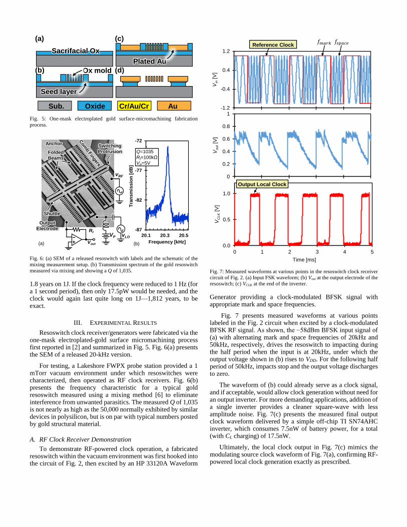
Resoswitch clock receiver/generators were fabricated via the one-mask electroplated-gold surface micromachining process first reported in [2] and summarized in Fig. 5. Fig. 6(a) presents the SEM of a released 20-kHz version.
For testing, a Lakeshore FWPX probe station provided a 1 mTorr vacuum environment under which resoswitches were characterized, then operated as RF clock receivers. Fig. 6(b) presents the frequency characteristic for a typical gold resoswitch measured using a mixing method [6] to eliminate interference from unwanted parasitics. The measured Q of 1,035 is not nearly as high as the 50,000 normally exhibited by similar devices in polysilicon, but is on par with typical numbers posted by gold structural material.
A. RF Clock Receiver Demonstration
To demonstrate RF-powered clock operation, a fabricated resoswitch within the vacuum environment was first hooked into the circuit of Fig. 2, then excited by an HP 33120A Waveform
Generator providing a clock-modulated BFSK signal with appropriate mark and space frequencies.
Fig. 7 presents measured waveforms at various points labeled in the Fig. 2 circuit when excited by a clock-modulated BFSK RF signal. As shown, the −58dBm BFSK input signal of (a) with alternating mark and space frequencies of 20kHz and 50kHz, respectively, drives the resoswitch to impacting during the half period when the input is at 20kHz, under which the output voltage shown in (b) rises to VDD. For the following half period of 50kHz, impacts stop and the output voltage discharges to zero.
The waveform of (b) could already serve as a clock signal, and if acceptable, would allow clock generation without need for an output inverter. For more demanding applications, addition of a single inverter provides a cleaner square-wave with less amplitude noise. Fig. 7(c) presents the measured final output clock waveform delivered by a simple off-chip TI SN74AHC inverter, which consumes 7.5nW of battery power, for a total (with CL charging) of 17.5nW.
Ultimately, the local clock output in Fig. 7(c) mimics the modulating source clock waveform of Fig. 7(a), confirming RF-powered local clock generation exactly as prescribed.
Fig. 6: (a) SEM of a released resoswitch with labels and the schematic of the
mixing measurement setup. (b) Transmission spectrum of the gold resoswitch
measured via mixing and showing a Q of 1,035.
Fig. 7: Measured waveforms at various points in the resoswitch clock receiver
circuit of Fig. 2. (a) Input FSK waveform; (b) Vout at the output electrode of the
resoswitch; (c) VCLK at the end of the inverter.
Sacrifacial Ox
Ox mold
Seed layer
Plated Au
Impact
Point
Output
50µm
Switch
Gap d0
Sub. Oxide Cr/Au/Cr Au
(a) (c)
(b) (d)
-87
-82
-77
-72
20.1 20.3 20.5
Tra
ns
mis
sio
n [
dB
]
Frequency [kHz]
Anchor
Shuttle
Folded
Beams
Output
Electrode
Switching
Protrusion
Rf
Vout
VP vLO
Q=1035
Rf=100kΩ
VP=5V
vRF
(a) (b)
0
0.2
0.4
0.6
0.8
1
Vout[V
]
0.0
0.5
1.0
0 1 2 3 4 5
VC
LK
[V]
Time [ms]
-1.2
-0.4
0.4
1.2
Vin
[V]
Reference Clock
Output Local Clock
B. Allan Deviation Measurements
To gauge the stability of the received and down-converted local clock, Fig. 8 presents the preliminary measured Allan deviation for the local clock when excited by an RF BPSK signal modulated by an HP33120A Waveform Generator against that of the reference clock used to modulate the input RF carrier. Clearly, the stability of the local clock signal is poorer than that of the reference clock. This is not unexpected given the stability discussion of Section II.C.
To explore the hypothesis of Section II.C that squegging can contribute to instability, Fig. 9 presents an oscilloscope snapshot of a few representative clock cycles at the Vout and VCLK nodes of Fig. 2. Here, squegging [7] leads to missed impacts every now and then, which then inserts unexpected fall and rise transitions, hence alters the frequency over this instance and compromises clock stability.
To further confirm this squegging-based source of instability, Fig. 10(a) and (b) present plots of the local RF-powered clock Allan deviation for varying values of input drive voltage vin and DC-bias VP. Given that larger drive voltage reduces squegging [5], the improvement in Allan deviation with increasing drive voltage seen in Fig. 10(a) does further attest to a squegging-based mechanism for instability. The Allan deviation dependence on DC-bias, on the other hand, is less conclusive, although there does seem to be a sweet spot at 8V where Allan deviation is best.
That squegging might be the principal reason for clock instability is actually encouraging, since recent research has identified methods by which squegging can be reduced. These include the use of a symmetric drive (which the Fig. 2 device already uses), reduction of the output impact gap [8], and the use of soft or compliant impact electrodes [5]. Work to incorporate these fixes into future resoswitch clock designs is underway that should lead to significant improvements in stability.
Fig. 8: Measured Allan deviation of the RF-powered clock generator alongside
that of the reference clock used to modulate the input RF carrier of the
HP33120A signal generator.
Fig. 9: Measured RF-powered clock generator output waveform, showing an
instance where squegging generates an undue clock transition, effectively
destabilizing the clock frequency.
Fig. 10: (a) Measured clock generator Allan deviation at various input voltage amplitudes vin while maintaining constant DC-bias VP at 9V. (b) Measured
Allan Deviation of the clock generator at different DC-bias values VP while
maintaining a constant drive voltage amplitude vin at 800mVpp.
1.E-09
1.E-07
1.E-05
1.E-03
1.E-01
5.E-03 5.E-02 5.E-01
σ
τ [sec]
Allan Deviation
MEMS CLK gen
HP33120A Ref CLK
0
0.4
0.8
1.2
2.5 3.5 4.5 5.5 6.5 7.5
Voltage [V
]
Time[ms]VCLK
Vout
Squegging Induces
Frequency Instability
vCLK
vout
1.E-06
1.E-04
1.E-02
1.E+00
5.E-03 5.E-02 5.E-01
Sig
ma
Tau [sec]
Allan Deviation VP=9V
Pin=-58dBm
Pin=-52dBm
Pin=-48dBm
1.E-05
1.E-03
1.E-01
5.E-03 5.E-02 5.E-01
Sig
ma
Tau [sec]
Allan Deviation vd=800mVpp
Vp=7V
Vp=8V
Vp=9V
(a)
(b)
IV. CONCLUSIONS
The 17.5nW of battery power used by the demonstrated RF-powered mechanical clock is already 57 times smaller than the
typical 1W RTC. If an on-chip inverter (with much less capacitance) were available, the total dynamic power consumption could potentially drop to only 5pW—15,000 times smaller. Since this power value would allow a 1J printed battery to last more than 6,000 years, battery self-discharge would more likely determine ultimate lifetime.
Although the demonstrated clock shares the accuracy of the modulating source clock, there are sources of instability that compromise the short-term performance of the local generated clock. Among the list of possible destabilizing phenomena, squegging seems to dominate in the demonstrated prototype. That squegging is the main culprit is somewhat encouraging, since it means there is opportunity for improvement, especially given the approaches to reducing resoswitch squegging already in the literature.
ACKNOWLEDGMENT
The authors are grateful for funding and support from the DARPA N-ZERO program.
REFERENCES
[1] E. Lee and J. Rabaey, "The Swarm at the Edge of the Cloud," IEEE Design & Test, vol. 31, no. June, pp. 8-20, June 2014.
[2] R. Liu, J. Naghsh Nilchi, T. Naing and C.-C. Nguyen, "Zero Quiescent Power VLF Mechanical Communication Receiver," in Transducers, Anchorage, 2015.
[3] W. Tang, T.-C. H. Nguyen, M. Judy and R. Howe, "Electro- static-comb drive of lateral polysilicon resonators," Sensors and Actuators, Vols. A21-23, pp. 328-331, 1990.
[4] R. Liu, J. Naghsh Nilchi, W.-C. Li and C.-C. Nguyen, "Soft-Impacting Micromechanical Resoswitch," in MEMS, Shanghai, 2016.
[5] A.-C. Wong and C.-C. Nguyen, "Micromechanical mixer-filters ("mixlers")," J. Microelectromech. Syst., vol. 13, no. Feb., pp. 100-112, 2004.
[6] S. Shaw and P. Holmes, "A periodically forced piecewise linear oscillator," Journal of Sound and Vibration, vol. 90, no. 1, pp. 129-155, 1983.
[7] Y. Lin, R. Liu, W.-C. Li and C.-C. Nguyen, "Polycide contact interface to suppress squegging in micromechanical resoswitches," in MEMS, San Francisco, 2014.
[8] Y. Lin, W.-C. Li, Z. Ren and C.-C. Nguyen, "The micromechanical resonant switch (“resoswitch”)”," in Hilton Head, 2008.