1/21/11 1 1 tanford araswat EE410 - 2011 Process and Device Simulations Krishna Saraswat Stanford University 2 tanford araswat EE410 - 2011 CMOS Process Flow Arsenic Mask 4 - Active PMOS shield. Arsenic implant for NMOS source /drain formation and gate doping. 7 Phosphosilicate glass deposition. Final "do-all" anneal. Mask 5 - Definition of contact holes Al/Si metallization by sputtering. Mask 6 - Patterning of Al/Si interconnect. 8 9 10 BF2 BF2 implant for PMOS source/ drain formation and gate doping. Phosphorus ions Phosphorus blanket substrate implant. Thin oxide and silicon nitride deposition. Mask 1- active area definition. 1 2 3 Field oxidation (LOCOS) 4 Mask 2 - P-well definition. boron p-well implant and drive- 5 Boron ions 6 Silicon nitride n-substrate p-well n+ source/drain Al/Si alloy p+ source/drain photoresist field oxide LTO-PSG thin oxide p-poly n-poly undoped poly Gate oxidation, gate a-Si deposition
Transcript
1/21/11
1
1 tanford araswat !
EE410 - 2011
Process and Device Simulations
Krishna Saraswat Stanford University
2 tanford araswat !
EE410 - 2011
CMOS Process Flow Arsenic
Mask 4 - Active PMOS shield. Arsenic implant for NMOS source/drain formation and gate doping.
7
Phosphosilicate glass deposition. Final "do-all" anneal. Mask 5 - Definition of contact holes
Al/Si metallization by sputtering.Mask 6 - Patterning of Al/Si interconnect.
8
9
10
BF2
BF2 implant for PMOS source/ drain formation and gate doping.
p-poly
n-poly
field oxide LTO-PSG
thin oxide
n-substrate p-well
n+ source/drain
Al/Si alloy
p+ source/drain photoresist
undoped poly
Silicon nitride
Fig. 1 (cont'd). CIS/CMOS-II process summary. Refer to text for details.
________________________________________________________________________ Appendix B: Pad Assignments 7
Phosphorus ions
Phosphorus blanket substrate implant.
Thin oxide and silicon nitride deposition.
Mask 1- active area definition.
1
2
3
Field oxidation (LOCOS)
4
Mask 2 - P-well definition. boron p-well implant and drive-
5
Boron ions
Amorphous-Si gate deposition.
6
Silicon nitride
n-substrate p-well
n+ source/drain
Al/Si alloy
p+ source/drain photoresist
field oxide LTO-PSG
thin oxide
p-poly
n-poly
undoped poly
Fig. 1. CIS/CMOS-II process summary. Refer to text for details.
________________________________________________________________________ Appendix B: Pad Assignments 6
Gate oxidation, gate a-Si deposition
1/21/11
2
3 tanford araswat !
EE410 - 2011
1. Analytical calculations based on EE212 a) Field and gate oxide thicknesses b) Ion implant profiles c) Junction depths d) Sheet resistance of junctions and poly-Si gate
- Mobility is a function of doping density. Use either Irwin’s curves or analytical model given in text books, for example in Pirret’s book.
- Note that mobility in poly-Si is lower. Assume half that of crystalline Si. - Dopant diffusivity in poly-Si is several orders of magnitude higher than crystalline Si
e) Threshold voltages 2. TSUPREM or Sentaurus simulations on the same topics as in 1 3. Comparison between analytical calculations and simulations
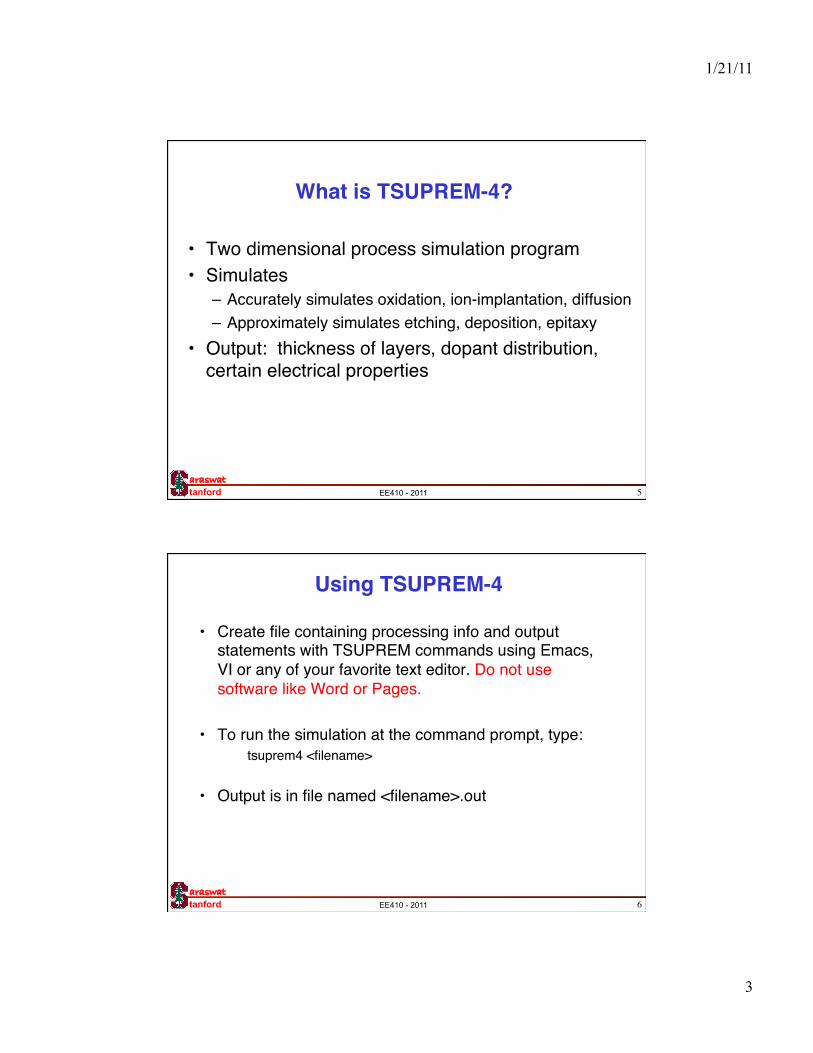
• Output: thickness of layers, dopant distribution, certain electrical properties"
6 tanford araswat !
EE410 - 2011
Using TSUPREM-4"
• Create file containing processing info and output statements with TSUPREM commands using Emacs, VI or any of your favorite text editor. Do not use software like Word or Pages. "
• To run the simulation at the command prompt, type:"" "tsuprem4 <filename>"
"• Output is in file named <filename>.out"
1/21/11
4
7 tanford araswat !
EE410 - 2011
Using TSUPREM-4 in 1-D mode: Gridding"
• We will use TSUPREM-4 in1-D mode, and grid the structure, e.g., in x-direction"
• Denser grid in areas where a lot of action occurs and where precision of information is important"
• i.e. thin layers, areas with steep dopant profiles"
8 tanford araswat !
EE410 - 2011
Creating a TSUPREM Input File"• Initialize (required before other steps)"
<100> Silicon, 5µm thick, .01µm grid spacing at top of layer, phosphorus concentration of 1e15"
Initialize <100> material=silicon width=5 dx=.01 – units in µm"+ phosphor=1e15 – Initialize Statement!Initialize <100> in.file=struct2 – Read structure from file struct2!
• Process steps"Diffusion with Transient Enhanced Diffusion effect:"
"Method PD.TRANS – diffusion model""Diffusion Temperature=1000 Time=10 DryO2– units in °C and minutes"
Diffusion with temperature ramp: ""Diffusion Temperature=800 T.Final=900 Time=20 Inert"
Examples of other steps""Deposition Thickness=0.6 Aluminum Dx=.02 Spaces=5""Implant Dose=5e15 Energy=45 BF2 Gaussian – units in cm-3 and keV""Etch oxide all"
1/21/11
5
9 tanford araswat !
EE410 - 2011
Creating a TSUPREM input file (2)"• Output commands"
Print Layers"Electrical – Lists out the thicknesses of the various layers and
their sheet resistance!Print Layers""Comment Vt measurement"+ Sweep bias from -10 to 10V in 0.2V step"+ Interface charge Qss concentration of 5e10 added"Electrical x=0 threshold nmos v=“-10 10 0.2”"+ " " Qss=5e10 (Default is 1e10/cm2)!+ " " Out.file=struct2"$ " " "Another way to do comments""Plot.1d electric "$This command plots the resistivity of the region under the
gate as a function of the voltage!
10 tanford araswat !
EE410 - 2011
$ EE410 Diode
$ This creates a simple diode
$ Initialize the siliconInitialize <100> material=Silicon width=5 dx=.01+ phosphor=1e15
$ Boron ImplantImplant Dose=5e15 Energy=45 BF2
$ Anneal using transient modelsmethod pd.transDiffusion Temperature=950 Time=30 Nitrogen
$ Grow 500nm field oxide.$ CIS furnaces use argon instead of nitrogen.Diffusion Time= 35 Temperature= 800 T.Rate=+5.714N i t r o g e nDiffusion Time= 10 Temperature=1000 DryO2Diffusion Time=100 Temperature=1000 WetO2Diffusion Time= 10 Temperature=1000 DryO2Diffusion Time= 35 Temperature=1000 T.Rate=-5.714 Nitrogen
$ Output results.Option device=postscript plot.out=”EE410Substrate.ps”Print L a y e r sS e l e c t z = l o g 1 0 ( a c t i v e ( p h o s p o r u s ) )P l o t . 1 d bottom=14 top=21 right=2
S a v e f i l e o u t . f i l e = c r e a t e _ s u b . s t r
Useful tips"• Create sub-structures (use loadfile or initialize to
load structure and savefile to save structure) • Skip steps (freckle etch) and ignore effects (layer
undercutting) that TSUPREM cannot simulate • Do not simulate furnace cycles below 800°C • Use gaussian or 2-gaussian implant profiles
instead of pearson profiles for all implants • See handout on CMOS-LOCOS Manual for more
details on TSUPREM • Simulation report will be due on 2/7/2011
18 tanford araswat !
EE410 - 2011
Writing the report"
• Donʼt spend your time trying to get your hand calculations to match your SUPREM results"
• Focus on differences between hand calculations and SUPREM results and explain why they are different"
1/21/11
10
19 tanford araswat !
EE410 - 2011
Getting help"
• Enter the following line in a file and run the file in TSUPREM. Help info will appear in the output file."help <command_name> "example: help implant ""Examples in the directory: /usr/class/ee410/examples"