Overview For over 40 years, designers of industrial process control systems and Analog Devices have worked together to define, develop, and deploy complete signal chain solutions, optimized for a wide array of applications. We bring reliability and innovation to this process with precision control and monitor- ing solutions based on our industry-leading technologies and systems-level expertise. Now you can quickly implement turnkey process control building blocks with Circuits from the Lab ™ reference circuits from Analog Devices. Circuits from the Lab reference circuits are engineered and tested for quick and easy system integra- tion to help solve today’s analog, mixed-signal, and RF design challenges. Each circuit is carefully documented with test data, design considerations, and evaluation setup; many circuits also include free design files and low cost evaluation hardware. Analog Devices has developed hundreds of reference circuits. This brochure includes a collection of these circuits specific to process control. Visit www.analog.com/circuits for the full collection. Contents Overview ....................... 1 PLC Challenges ................. 2 Input Module ................... 4 Output Module ................. 10 Industrial Automation ............ 15 PLC Reference Design ........... 19 Circuits from the Lab Reference Circuit Tips ........... 20 Process Control Circuits from the Lab Reference Circuits www.analog.com/circuitsPCTL-br
Transcript
OverviewFor over 40 years, designers of industrial process control systems and Analog Devices have worked together to define, develop, and deploy complete signal chain solutions, optimized for a wide array of applications. We bring reliability and innovation to this process with precision control and monitor-ing solutions based on our industry-leading technologies and systems-level expertise. Now you can quickly implement turnkey process control building blocks with Circuits from the Lab™ reference circuits from Analog Devices.
Circuits from the Lab reference circuits are engineered and tested for quick and easy system integra-tion to help solve today’s analog, mixed-signal, and RF design challenges. Each circuit is carefully documented with test data, design considerations, and evaluation setup; many circuits also include free design files and low cost evaluation hardware.
Analog Devices has developed hundreds of reference circuits. This brochure includes a collection of these circuits specific to process control. Visit www.analog.com/circuits for the full collection.
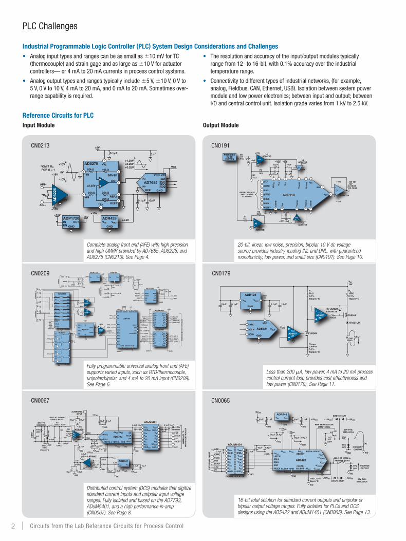
Complete analog front end (AFE) with high precision and high CMRR provided by AD7685, AD8226, and AD8275 (CN0213). See Page 4.
Fully programmable universal analog front end (AFE) supports varied inputs, such as RTD/thermocouple, unipolar/bipolar, and 4 mA to 20 mA input (CN0209). See Page 6.
Distributed control system (DCS) modules that digitize standard current inputs and unipolar input voltage ranges. Fully isolated and based on the AD7793, ADuM5401, and a high performance in-amp (CN0067). See Page 8.
PLC Challenges
Industrial Programmable Logic Controller (PLC) System Design Considerations and Challenges• Analog input types and ranges can be as small as ±10 mV for TC
(thermocouple) and strain gage and as large as ±10 V for actuator controllers— or 4 mA to 20 mA currents in process control systems.
• Analog output types and ranges typically include ±5 V, ±10 V, 0 V to 5 V, 0 V to 10 V, 4 mA to 20 mA, and 0 mA to 20 mA. Sometimes over-range capability is required.
• The resolution and accuracy of the input/output modules typically range from 12- to 16-bit, with 0.1% accuracy over the industrial temperature range.
• Connectivity to different types of industrial networks, (for example, analog, Fieldbus, CAN, Ethernet, USB). Isolation between system power module and low power electronics; between input and output; between I/O and central control unit. Isolation grade varies from 1 kV to 2.5 kV.
Reference Circuits for PLCInput Module Output Module
ADR125
AD5621
VIN VOUT
GND
AD8657
AD8657
SYNC
SCLK
SDIN
VDD
VOUTVDAC
GNDIRFU024N
RSENSE2.49k0.1%10ppm/°C
R11k0.1%10ppm/°C
R21000.1%10ppm/°C
RLOAD250
BAS21LT1
IRFU9014
10F0.1F0.1F10F
1/2
A1
1/2
A2
18V ZENERBZX84C18
VSY18V
IOUT
VREF5V
100
VDD2
GND2
VOADVCC
DVCCSELECT
VIN VOUT
VOUT
RSET
AVDD
+VSENSE
–VSENSE
0V
3.3V
DINDOUT
SCLK
SYNC
3.3V0.1F
VOBVOC SDIN
SDO
FAULT CLEAR GNDCLEARSELECT
VID
VE2
GND2
VDD1
GND1
VIA
VIB
VIC
VOD
VE1
GND1
+
0.1F
600 AT 100MHzFERRITE BEAD
TVS20V
20V TVS:SMBJ20CA
TVS20V
15VISO
+5VISO10F 0.1F
ISO
ISO
ISO
ISO
ISOISOISO
ISO
22nF
1k 10
15k, 0.1%5ppm/°C
BC
E
+ 10F 0.1F
+ 10F 0.1F
ISO
+ 10F 0.1F
ISO
+ 10F 0.1F
ISO
ISO
LATCHSCLK AD5422
ADuM1401
DIGITAL ISOLATOR
EX
TE
RN
AL
INP
UT
ADR445
AVSS REFIN BOOST
+15VISO –15VISO
+15VISO –15VISO
BAS70-04LT1
4nF
CCOMP
+15VISO –15VISO
BAS70-04LT1
NPN TRANSISTOR:MMBT8099L
20V TVS:SMBJ20CA
CURRENTOUTPUT
VOLTAGEOUTPUT
ISO
RL
IOUT
20-bit, linear, low noise, precision, bipolar 10 V dc voltage source provides industry-leading INL and DNL, with guaranteed monotonicity, low power, and small size (CN0191). See Page 10.
Less than 200 μA, low power, 4 mA to 20 mA process control current loop provides cost effectiveness and low power (CN0179). See Page 11.
16-bit total solution for standard current outputs and unipolar or bipolar output voltage ranges. Fully isolated for PLCs and DCS designs using the AD5422 and ADuM1401 (CN0065). See Page 13.
2 | Circuits from the Lab Reference Circuits for Process Control
Industrial Automation
AD7982AD8475
20V
–10V
0V
+10V
+7V TO +18V
+0.5V
+2.5V
+4.5V
NC
NC
+IN 0.4x
–IN 0.4x
+IN 0.8x
–IN 0.8x
4V
+0.5V
2.5V
+4.5V
4V
–OUTIN–
IN++OUT
VOCM
+VS
+5V
–VS
ADR435
20
20
270pF
270pF
1.3nF
VIO
CNVGNDREF
VDD
SDO
SCK
SDI
+5V
+2.5V +1.8V TO +5V
10k
10k0.1F
+5V
1k
ADuC7061
P1.
1/S
OU
T
P1.
0/S
IN
IEXC0AVDD DVDD
ADC0
RxD
RxD
TxD
TxD
/RST
nTRST/BM
S2
S1
VREF +
RREF
VREF –
ADC1
5.62k0.1%
100PtRTD
ADC2
THERMOCOUPLEJUNCTION
ADC3
DACGND
BEAD
2.5V
BEAD
USB HEADER
1k10
10
10
0.01F
0.01F
0.1F
4.7F4.7F
0.1F4.7F
IN5V
D–
D+
GND
OUT
ADP3333-2.5
FT232R
BEAD
FERRITE BEADS:1k @ 100MHzTAIYO YUDENBK2125HS102-T
0.1FSHIELD
CN0214 CN0180
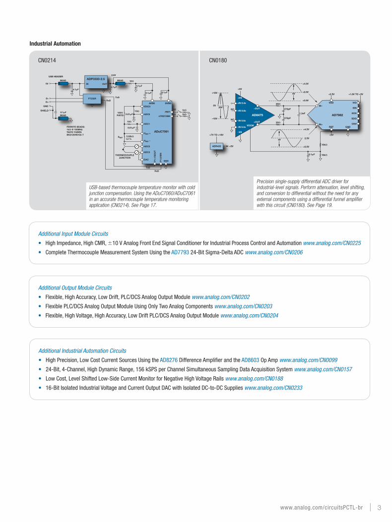
USB-based thermocouple temperature monitor with cold junction compensation. Using the ADuC7060/ADuC7061 in an accurate thermocouple temperature monitoring application (CN0214). See Page 17.
Precision single-supply differential ADC driver for industrial-level signals. Perform attenuation, level shifting, and conversion to differential without the need for any external components using a differential funnel amplifier with this circuit (CN0180). See Page 19.
Additional Industrial Automation Circuits
• High Precision, Low Cost Current Sources Using the AD8276 Difference Amplifier and the AD8603 Op Amp www.analog.com/CN0099
• 24-Bit, 4-Channel, High Dynamic Range, 156 kSPS per Channel Simultaneous Sampling Data Acquisition System www.analog.com/CN0157
• Low Cost, Level Shifted Low-Side Current Monitor for Negative High Voltage Rails www.analog.com/CN0188
• 16-Bit Isolated Industrial Voltage and Current Output DAC with Isolated DC-to-DC Supplies www.analog.com/CN0233
Additional Output Module Circuits
• Flexible, High Accuracy, Low Drift, PLC/DCS Analog Output Module www.analog.com/CN0202
• Flexible PLC/DCS Analog Output Module Using Only Two Analog Components www.analog.com/CN0203
• Flexible, High Voltage, High Accuracy, Low Drift PLC/DCS Analog Output Module www.analog.com/CN0204
Additional Input Module Circuits
• High Impedance, High CMR, ±10 V Analog Front End Signal Conditioner for Industrial Process Control and Automation www.analog.com/CN0225
• Complete Thermocouple Measurement System Using the AD7793 24-Bit Sigma-Delta ADC www.analog.com/CN0206
Complete, High Speed, High CMRR Precision Analog Front End (AFE) for Process Control (CN0213)
Author: Colm Slattery—Systems Applications Engineer, Industrial and Instrumentation
Circuit Function and Benefits
Signal levels in industrial process control systems generally fall into one of the following categories: single-ended current (4 mA to 20 mA), single-ended, differential voltage (0 V to 5V, 0 V to 10 V, ±5 V, ±10 V), or small signal inputs from sensors such as thermocouples or load cells. Large common-mode voltage swings are also typical, especially for small signal differential inputs; therefore good common-mode rejection is an important specification in the analog signal processing system.
The analog front-end circuit shown in is optimized for high precision and high common-mode rejection ratio (CMRR) when pro-cessing these types of industrial-level signals. The circuit level shifts and attenuates the signals so they are compatible with the input range requirements of most modern single-supply SAR ADCs, such as the AD7685 high performance 16-bit, 250 kSPS PulSAR® ADC. With an 18 V p-p input signal, the circuit achieves approximately 105 dB common-mode rejection (CMR) at 100 Hz and 80 dB CMR at 5 kHz.
High precision, high input impedance, and high CMR are provided by the AD8226 instrumentation amplifier. For high precision applications, a high input impedance is required to minimize system gain errors and also to achieve good CMR. The AD8226 gain is resistor-programmable from 1 to 1000.
A resistive level shifter/attenuator stage directly on the input would inevitably degrade CMR performance due to the mismatch between the resistors. The AD8226 provides the excellent CMR required for both small signal and large signal inputs. The AD8275 level shifter/attenuator/driver performs the attenuation and level shifting function in the circuit, without any need for external components.
Traditionally, Σ-∆ ADCs have been used in high resolution measurement systems because signal bandwidths are quite low, and the Σ-∆ architecture provides excellent noise performance at low update rates. However, there is an increased trend for higher update rates, especially in multichannel systems, to allow faster per-channel update, or for increased channel density. In such cases a high performance SAR ADC is a good alternative. The circuit uses the AD7685 250 kSPS, 16-bit ADC, with the AD8226 high performance in-amp, and the AD8275 attenuator/level shifter amplifier implemented as a complete system solution without the need for any external components.
Circuit Description
This circuit is comprised of an AD8226 rail-to-rail output in-amp, connected to the positive input of the AD8275 G = 0.2 difference amplifier, whose output is then connected to the input of the AD7685, a 16-bit, 250 kSPS PulSAR ADC in MSOP/QFN. The AD8226 is set for a gain-of-one mode (high voltage/cur-rent inputs), and its output is referenced to ground. Single-ended or differential inputs can be used. The output of the AD8226 is a bipolar signal, which drives the AD8275 input. The AD8275 acts to attenuate and level shift the bipolar input, providing for a gain of 0.2. Hence, differential inputs of 20 V p-p at its inputs will yield a 4 V p-p single-ended range on the output. The ADR439 precision 4.5 V reference is used to provide both the internal common-mode bias voltage for the AD8275 (VREF/2 = 2.25 V), as well as the external reference voltage for the AD7685 ADC. Under these conditions, the output of the AD8275 swings from +0.25 V to +4.25 V, which is within the range of the AD7685, 0 V to +4.5 V.
The ADP1720 is used to provide the 5 V supply for the AD8275 and the AD7685. The ADP1720 was chosen because it has a high input voltage range (up to 28 V). In this circuit, the ADP1720 is only required to supply approximately 4 mA to the AD8275 and AD7685, so the worst case power dissipation in the regulator with 28 V input is about 90 mW. This allows the complete system to run from the external ±15 V supplies.
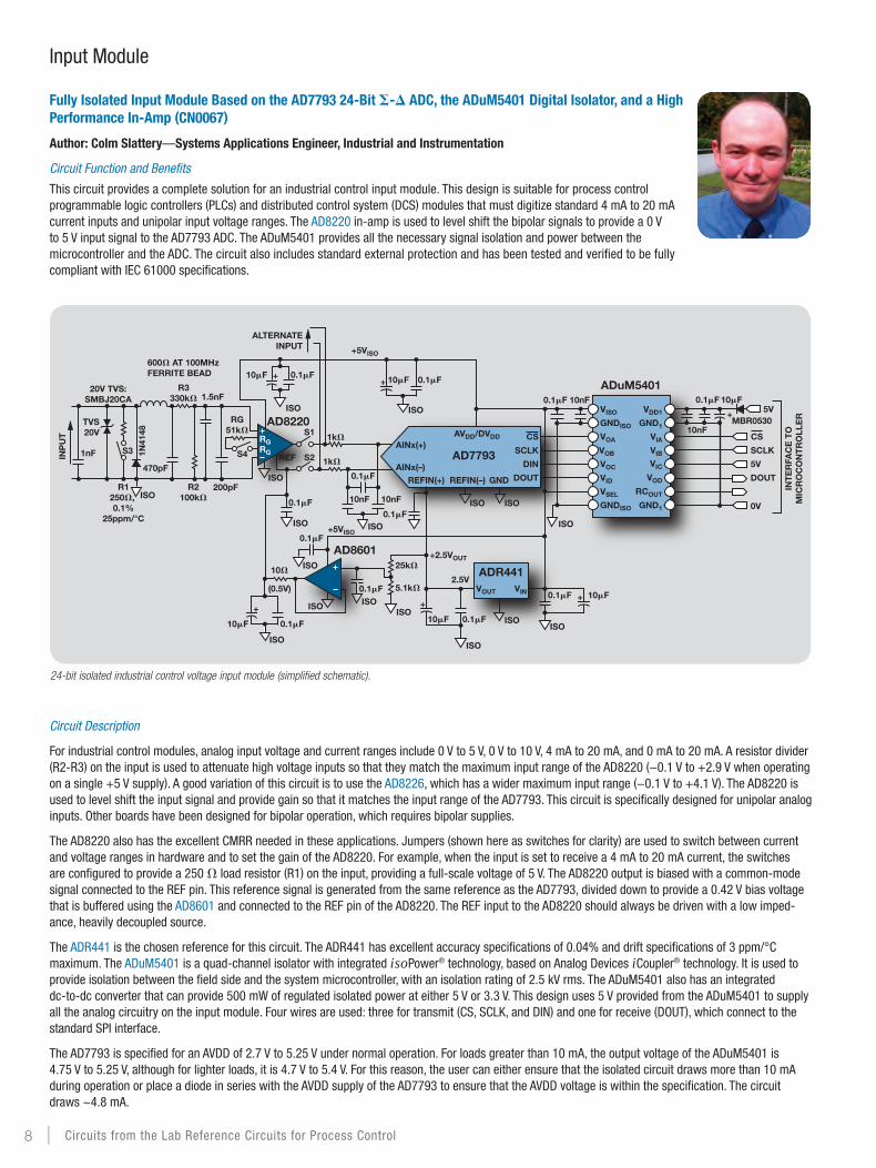
24-bit isolated industrial control voltage input module (simplified schematic).
AD82757
5
6
8
250k
0.1F
50k
20k
20k
10k
3
+IN
–IN
REF2
REF1–VS
+VS
+5V
OUT
SENSE
1F
10F
AD7685
VDD
GNDREF
IN+
IN–
ADP1720
VIOSDI
SCKSDOCNV
+15V
−15V
+15V+15V
+5V+4.5V
+4.25V+2.25V+0.25V
ADR439
+10V
−10V
0V
AD
8226
VIO
+2.25V
0.1F
INEN
OUT
GND
VIN VOUT
GND
AIN+
AIN−
*RG
*OMIT RG FOR G = 1
REF 1
4
4 | Circuits from the Lab Reference Circuits for Process Control
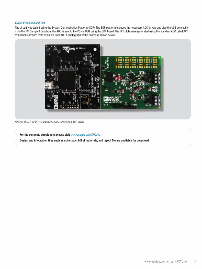
The circuit was tested using the System Demonstration Platform (SDP). The SDP platform includes the necessary ADC drivers and also the USB connectiv-ity to the PC. Sampled data from the ADC is sent to the PC via USB using the SDP board. The FFT plots were generated using the standard ADC LabVIEW®
evaluation software tools available from ADI. A photograph of the boards is shown below.
Photo of EVAL-A-INPUT-1AZ evaluation board connected to SDP board.
For the complete circuit note, please visit www.analog.com/CN0213.
Design and integration files such as schematic, bill of materials, and layout file are available for download.
www.analog.com/circuitsPCTL-br | 5
Input Module
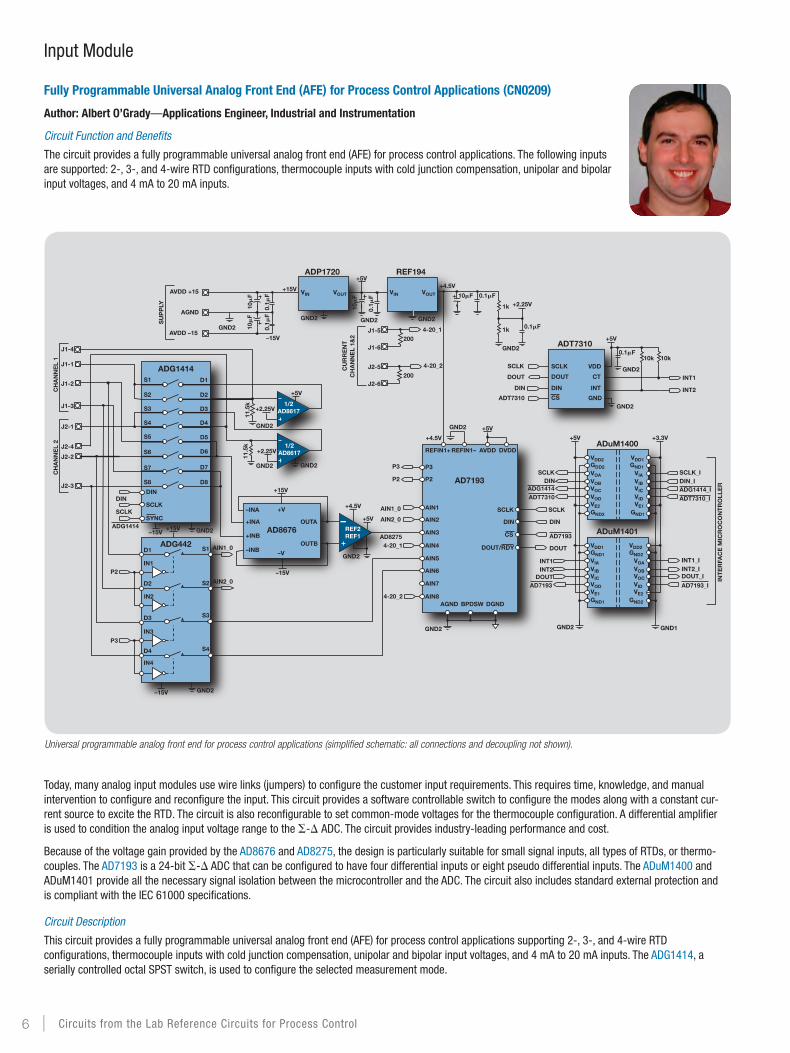
Fully Programmable Universal Analog Front End (AFE) for Process Control Applications (CN0209)
Author: Albert O’Grady—Applications Engineer, Industrial and Instrumentation
Circuit Function and Benefits
The circuit provides a fully programmable universal analog front end (AFE) for process control applications. The following inputs are supported: 2-, 3-, and 4-wire RTD configurations, thermocouple inputs with cold junction compensation, unipolar and bipolar input voltages, and 4 mA to 20 mA inputs.
Today, many analog input modules use wire links (jumpers) to configure the customer input requirements. This requires time, knowledge, and manual intervention to configure and reconfigure the input. This circuit provides a software controllable switch to configure the modes along with a constant cur-rent source to excite the RTD. The circuit is also reconfigurable to set common-mode voltages for the thermocouple configuration. A differential amplifier is used to condition the analog input voltage range to the Σ-∆ ADC. The circuit provides industry-leading performance and cost.
Because of the voltage gain provided by the AD8676 and AD8275, the design is particularly suitable for small signal inputs, all types of RTDs, or thermo-couples. The AD7193 is a 24-bit Σ-∆ ADC that can be configured to have four differential inputs or eight pseudo differential inputs. The ADuM1400 and ADuM1401 provide all the necessary signal isolation between the microcontroller and the ADC. The circuit also includes standard external protection and is compliant with the IEC 61000 specifications.
Circuit Description
This circuit provides a fully programmable universal analog front end (AFE) for process control applications supporting 2-, 3-, and 4-wire RTD configurations, thermocouple inputs with cold junction compensation, unipolar and bipolar input voltages, and 4 mA to 20 mA inputs. The ADG1414, a serially controlled octal SPST switch, is used to configure the selected measurement mode.
Universal programmable analog front end for process control applications (simplified schematic: all connections and decoupling not shown).
INT
ER
FAC
E M
ICR
OC
ON
TR
OLL
ER
P3
P2
AIN1
AIN2
AIN3
AIN4
AIN5
AIN6
AIN7
AIN8
SCLK
DIN
REFIN1+ REFIN1– AVDD DVDD
DOUT/RDY
CS
ADP1720
AD7193
AD8275AD8676
–INA
–INB
+INA
+INB
OUTA
OUTB
+V
–V
+5V
+5V
+15V
–15V
1/2AD8617
+4.5V
REF2REF1
AGND
+4.5V
REF194
+4.5V
+5V
11.5
k11
.5k
1k
1k
+2.25V
0.1F
+2.25V
+2.25V
0.1
F
DGNDBPDSW
0.1F10F
10
F
ADuM1400
VDD2GDD2VOAVOBVOCVODVE2GND2
VDD1
VIA
GND1
VIBVICVIDVE1
GND1
ADuM1401
VDD1GND1VIAVIBVICVODVE1GND1
VDD2
VOA
GND2
VOBVOCVIDVE2
GND2
ADG1414D1
D2
D3
D4
D5
D6
D7
D8
S1
S2
S3
S4
S5
S6
S7
S8
+15V
–15V
–15V
DIN
SCLKDIN
SCLKSYNC
SCLK_IDIN_IADG1414_IADT7310_I
INT1_IINT2_IDOUT_I
AD7193_I
INT1INT2
DOUTAD7193
SCLKDIN
ADG1414ADT7310
+5V
GND2
SCLK
AD7193
DIN
DOUT
+5V +3.3V
GND2 GND1
+15V
–15V
ADG1414
P3
P2
AIN1_0
AIN1_0
AIN2_0
J1-4
J1-1
J1-2
J1-3
J2-3
J2-2
J2-1
J2-4
CH
AN
NE
L 1
CH
AN
NE
L 2
ADT7310
SCLK
DOUT
SCLK
DOUT
ADT7310
DIN DIN
CS
VDD
CT
INT
GND
+5V
10k 10k
INT1
INT2
AVDD +15
AGND
AVDD –15
10
F10
F
SU
PP
LY
J1-5
J1-6
J2-5
J2-6
200
200
4-20_1
4-20_2
4-20_1
4-20_2
CH
AN
NE
L 1&
2C
UR
RE
NT
ADG442
IN1
S1D1
P2
P3
AIN2_0
S3
S2
S4D4
D3
D2
IN4
IN3
IN2
GND2
GND2
GND2GND2GND2
GND2
GND2
GND2
GND2
GND2
GND2
GND2
GND2
GND2
1/2AD8617
VIN VOUTVIN VOUT
0.1F
0.1
F0.
1F +
6 | Circuits from the Lab Reference Circuits for Process Control
This circuit supports the measurement of unipolar and bipolar signal ranges up to ±10 V. The input signal goes through a signal conditioning stage before conversion by the AD7193 ADC. The AD8676 amplifier buffers the inputs before the gain stage. The AD8275 is used to level shift the input signal and provides gain so that it matches the input range of the AD7193. The AD8275 output is biased with a common-mode voltage connected to its REF pin. This voltage is generated by the REF194 precision 4.5 V reference.
RTD Measurement
This circuit supports 2-, 3-, and 4-wire RTD configurations. In this case, the transducer is a 1000 Ω platinum (Pt) RTD (resistive temperature device). The most accurate arrangement is a 4-lead RTD configuration. In the application shown, an external 200 μA current source provides the excitation current for the RTD, and the AD7193 is operated at gain of 16 to maximize the dynamic range in the circuit. The AD8617 amplifier is configured as a current source when the RTD measurement mode is selected. It is reconfigured in closed-loop to set the common-mode voltage when the thermocouple measurement is selected. The AD8617 is a dual low noise amplifier so that it can drive both input channels available on the board. The resistor configuring the current source must have a low temperature coefficient to avoid drift errors in the measurement circuit.
Thermocouple Measurement
In a thermocouple application, the voltage generated by the thermocouple is measured with respect to an absolute reference, provided externally to the ADC. The cold junction compensation is implemented using the ADT7310 16-bit temperature sensor. Because the signal from the thermocouple is small, and to maximize the dynamic range in the circuit, the AD7193 is operated at its highest gain range of 128. Because the input channel is buffered, large decoupling capacitors can be placed on the front end, if required, to eliminate any noise pickup that may be present in the thermocouple leads. The common-mode voltage for the thermocouple measurement is provided by the AD8617 amplifier.
4 mA to 20 mA Current Measurement
This circuit also supports 4 mA to 20 mA current measurement. The current is converted to a voltage using an on-board sense resistor. To use the full dynamic range of the ADC in the current measurement mode, a 200 Ω resistor is used. The sense resistor must have a low temperature coefficient to avoid temperature drift errors in the measurement circuit.
Regulator and Reference Selection
The ADP1720 was chosen as the 5 V regulator for this circuit. The ADP1720 is a high voltage micropower linear regulator particularly suitable for industrial application. The 4.5 V REF194 was chosen as the reference for this circuit, and the E-grade device has an initial accuracy ±2 mV at 25°C and a drift of 5 ppm/°C maximum. It is a low dropout device and consumes less than 45 μA, with performance specifications over −40°C to +125°C.
Isolation
The ADuM1400 and the ADuM1401 are quad-channel digital isolators based on Analog Devices’ iCoupler® technology. These are used to provide isolation between the field side and the system microcontroller, with an isolation rating of 2.5 kV rms. Four wires are used through the ADuM1400, all for transmit (SCLK, DIN, ADG1414, ADT7310). Four wires are used through the ADuM1401: one for transmit (AD7193) and three for receive (INT1, INT2, DOUT). The DIN, DOUT, and SCLK lines are connected to the SPORT interface.
Circuit Evaluation and Test
This circuit uses the EVAL-CN0209-SDPZ circuit board and the EVAL-SDP-CB1Z System Demonstration Platform (SDP) evaluation board. The two boards have 120-pin mating connectors, allowing for the quick setup and evaluation of the circuit’s performance. The EVAL-CN0209-SDPZ board contains the circuit to be evaluated, as described in this note, and the SDP evaluation board is used with the CN0209 evaluation software to capture the data from the EVAL-CN0209-SDPZ circuit board.
For the complete circuit note, please visit www.analog.com/CN0209.
Design and integration files such as schematic, bill of materials, and layout file are available for download, and low cost circuit evaluation hardware is available for purchase.
Fully Isolated Input Module Based on the AD7793 24-Bit 𝚺-𝚫 ADC, the ADuM5401 Digital Isolator, and a High Performance In-Amp (CN0067)
Author: Colm Slattery—Systems Applications Engineer, Industrial and Instrumentation
Circuit Function and Benefits
This circuit provides a complete solution for an industrial control input module. This design is suitable for process control programmable logic controllers (PLCs) and distributed control system (DCS) modules that must digitize standard 4 mA to 20 mA current inputs and unipolar input voltage ranges. The AD8220 in-amp is used to level shift the bipolar signals to provide a 0 V to 5 V input signal to the AD7793 ADC. The ADuM5401 provides all the necessary signal isolation and power between the microcontroller and the ADC. The circuit also includes standard external protection and has been tested and verified to be fully compliant with IEC 61000 specifications.
Circuit Description
For industrial control modules, analog input voltage and current ranges include 0 V to 5 V, 0 V to 10 V, 4 mA to 20 mA, and 0 mA to 20 mA. A resistor divider (R2-R3) on the input is used to attenuate high voltage inputs so that they match the maximum input range of the AD8220 (−0.1 V to +2.9 V when operating on a single +5 V supply). A good variation of this circuit is to use the AD8226, which has a wider maximum input range (−0.1 V to +4.1 V). The AD8220 is used to level shift the input signal and provide gain so that it matches the input range of the AD7793. This circuit is specifically designed for unipolar analog inputs. Other boards have been designed for bipolar operation, which requires bipolar supplies.
The AD8220 also has the excellent CMRR needed in these applications. Jumpers (shown here as switches for clarity) are used to switch between current and voltage ranges in hardware and to set the gain of the AD8220. For example, when the input is set to receive a 4 mA to 20 mA current, the switches are configured to provide a 250 Ω load resistor (R1) on the input, providing a full-scale voltage of 5 V. The AD8220 output is biased with a common-mode signal connected to the REF pin. This reference signal is generated from the same reference as the AD7793, divided down to provide a 0.42 V bias voltage that is buffered using the AD8601 and connected to the REF pin of the AD8220. The REF input to the AD8220 should always be driven with a low imped-ance, heavily decoupled source.
The ADR441 is the chosen reference for this circuit. The ADR441 has excellent accuracy specifications of 0.04% and drift specifications of 3 ppm/°C maximum. The ADuM5401 is a quad-channel isolator with integrated isoPower® technology, based on Analog Devices iCoupler® technology. It is used to provide isolation between the field side and the system microcontroller, with an isolation rating of 2.5 kV rms. The ADuM5401 also has an integrated dc-to-dc converter that can provide 500 mW of regulated isolated power at either 5 V or 3.3 V. This design uses 5 V provided from the ADuM5401 to supply all the analog circuitry on the input module. Four wires are used: three for transmit (CS, SCLK, and DIN) and one for receive (DOUT), which connect to the standard SPI interface.
The AD7793 is specified for an AVDD of 2.7 V to 5.25 V under normal operation. For loads greater than 10 mA, the output voltage of the ADuM5401 is 4.75 V to 5.25 V, although for lighter loads, it is 4.7 V to 5.4 V. For this reason, the user can either ensure that the isolated circuit draws more than 10 mA during operation or place a diode in series with the AVDD supply of the AD7793 to ensure that the AVDD voltage is within the specification. The circuit draws ~4.8 mA.
24-bit isolated industrial control voltage input module (simplified schematic).
VDD1
GND1
VIA
VOUT VIN
VIB
VIC
VOD
RCOUT
GND1
VISO
GNDISO
VOB
VOC
VID
VSEL
GNDISO
+
10nF
0.1F 10F
+2.5VOUT
+5VISO
+5VISO
10F0.1F
ISOISO
ISO
0.1F
+MBR0530
0.1F 10nF
ISO
ISOISO
ISO
ISO
ISOISO ISO
2.5V
+ 10F10F 0.1F
ISO
+ 0.1F
ISO
+
10F 0.1F
ISO
ISOISO
0.1F
10nF 10nF
1nF
470pF
1.5nF
200pF
1N41
48
TVS20V
20V TVS:SMBJ20CA
600 AT 100MHzFERRITE BEAD
S3
S1 1k
1k
25k
5.1k
S2S4
R3330k
R2100k
R1250, 0.1%
25ppm/°C
RG51k
0.1F
0.1F
ADuM5401
ALTERNATEINPUT
INP
UT
INT
ER
FAC
E T
OM
ICR
OC
ON
TR
OLL
ER
ADR441
CS
SCLK
DIN
DOUT
CS
SCLK
5V
DOUT
0V
5V
VOA
GND
AD7793
AD8220
AD8601
RGRG
REF
+
10F 0.1F
0.1F
ISO
10
(0.5V)
AINx(+)
AINx(–)
AVDD/DVDD
REFIN(+) REFIN(–)
8 | Circuits from the Lab Reference Circuits for Process Control
Shown bleow is a noise plot of the input module when a 2.5 V input signal is connected using the 0 V to +10 V input range. The measured noise on the output is in peak-to-peak resolution. The 19.5 bit peak-to-peak noise-free code resolution means there are 4.5 bits of noise flicker on the output of the ADC with respect to the ADC’s 24-bit resolution. Therefore, the ADC’s noise-free code resolution is 19.5 bits. In terms of contributing to the overall system error, the measured noise of 4.5 bits contributes ~0.00014% error with respect to the full-scale range of the ADC. The integral nonlinearity error of the AD7793 is 0.0015%.
Input module histogram, 4.7 Hz update rate, gain = 1, input = 2.5 V reference.
For the complete circuit note, please visit www.analog.com/CN0067.
Linux driver for AD7792 and AD7793 is available for download.
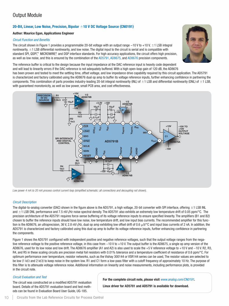
20-Bit, Linear, Low Noise, Precision, Bipolar ±10 V DC Voltage Source (CN0191)
Author: Maurice Egan, Applications Engineer
Circuit Function and Benefits
The circuit shown in Figure 1 provides a programmable 20-bit voltage with an output range −10 V to +10 V, ±1 LSB integral nonlinearity, ±1 LSB differential nonlinearity, and low noise. The digital input to the circuit is serial and is compatible with standard SPI, QSPI™, MICROWIRE®, and DSP interface standards. For high accuracy applications, the circuit offers high precision, as well as low noise, and this is ensured by the combination of the AD5791, AD8675, and AD8676 precision components.
The reference buffer is critical to the design because the input impedance at the DAC reference input is heavily code dependent and will lead to linearity errors if the DAC reference is not adequately buffered. With a high open-loop gain of 120 dB, the AD8676 has been proven and tested to meet the settling time, offset voltage, and low impedance drive capability required by this circuit application. The AD5791 is characterized and factory calibrated using the AD8676 dual op amp to buffer its voltage reference inputs, further enhancing confidence in partnering the components. This combination of parts provides industry-leading 20-bit integral nonlinearity (INL) of ±1 LSB and differential nonlinearity (DNL) of ±1 LSB, with guaranteed monotonicity, as well as low power, small PCB area, and cost effectiveness.
Circuit Description
The digital-to-analog converter (DAC) shown in the figure above is the AD5791, a high voltage, 20-bit converter with SPI interface, offering ±1 LSB INL and ±1 LSB DNL performance and 7.5 nV/√Hz noise spectral density. The AD5791 also exhibits an extremely low temperature drift of 0.05 ppm/°C. The precision architecture of the AD5791 requires force-sense buffering of its voltage reference inputs to ensure specified linearity. The amplifiers (B1 and B2) chosen to buffer the reference inputs should have low noise, low temperature drift, and low input bias currents. The recommended amplifier for this func-tion is the AD8676, an ultraprecision, 36 V, 2.8 nV/√Hz, dual op amp exhibiting low offset drift of 0.6 μV/°C and input bias currents of 2 nA. In addition, the AD5791 is characterized and factory calibrated using this dual op amp to buffer its voltage reference inputs, further enhancing confidence in partnering the components.
Figure 1 shows the AD5791 configured with independent positive and negative reference voltages, such that the output voltage ranges from the nega-tive reference voltage to the positive reference voltage, in this case from −10 V to +10 V. The output buffer is the AD8675, a single op amp version of the AD8676, used for its low noise and low drift. The AD8676 amplifier (A1 and A2) is also used to scale the +5 V reference voltage to +10 V and −10 V. R2, R3, R4, and R5 in these scaling circuits are precision metal foil resistors with 0.01% tolerance and a temperature coefficient of resistance of 0.6 ppm/°C. For optimum performance over temperature, resistor networks, such as the Vishay 300144 or VSR144 series can be used, The resistor values are selected to be low (1 kΩ and 2 kΩ) to keep noise in the system low. R1 and C1 form a low-pass filter with a cutoff frequency of approximately 10 Hz. The purpose of this filter is to attenuate voltage reference noise. Additional information on linearity and noise measurements, including performance plots, is provided in the circuit note.
Circuit Evaluation and Test
The circuit was constructed on a modified AD5791 evaluation board. Details of the AD5791 evaluation board and test meth-ods can be found in Evaluation Board User Guide, UG-185.
Low power 4 mA to 20 mA process control current loop (simplified schematic: all connections and decoupling not shown).
AD5791B
VR
EFP
F
VR
EFP
S
VR
EFN
F
RFB
INVV
RE
FNS
1/2AD8676B
1/2AD8676B
AG
ND
DG
ND
VS
S
VOUT
IOV
CC
VC
C
VD
D7
8
11
14
13
12
6
2
1
2034510
15 18 16 19
CLR
LDAC
SDO
SYNC
SCLK
SDIN
RESET
+
+
+
+15V+3.3V
–15V
+
AD8675A
1/2AD8676B
1/2AD8676B
+ –
+ –
+
–
A1
C1
B1
B2
PRECISION5V DC
SOURCE
SPI INTERFACEAND DIGITAL
CONTROL
–10V TO +10VOUTPUTVOLTAGE
0.1F
10F
10F 10F
0.1F 0.1F
10F
1k
R1
1.5k
R3
2kR5
R21k
C1
+15V
−15V
+15V
−15V
+15V −15V
+
–
+
–A2
1kR4
9
17
For the complete circuit note, please visit www.analog.com/CN0191.
Linux driver for AD5781 and AD5791 is available for download.
10 | Circuits from the Lab Reference Circuits for Process Control
Less Than 200 𝛍A, Low Power, 4 mA to 20 mA, Process Control Current Loop (CN0179)
Author: Vicky Wong— Applications Engineer, Precision Amplifiers and References
Circuit Function and Benefit
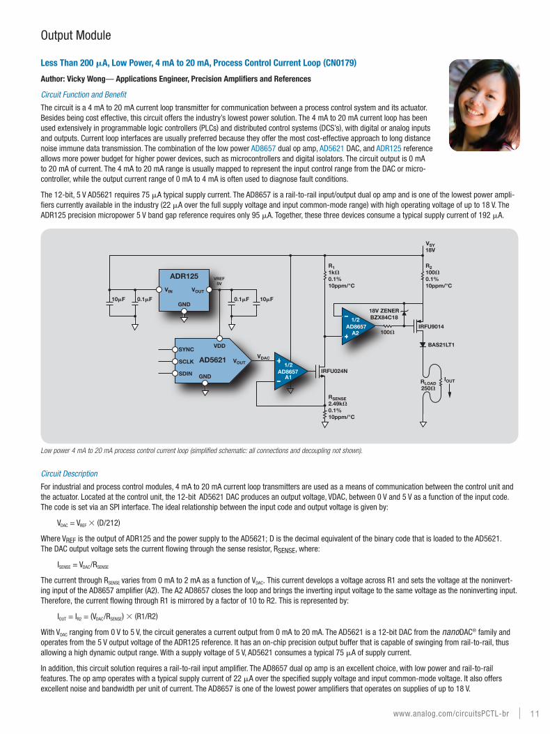
The circuit is a 4 mA to 20 mA current loop transmitter for communication between a process control system and its actuator. Besides being cost effective, this circuit offers the industry’s lowest power solution. The 4 mA to 20 mA current loop has been used extensively in programmable logic controllers (PLCs) and distributed control systems (DCS’s), with digital or analog inputs and outputs. Current loop interfaces are usually preferred because they offer the most cost-effective approach to long distance noise immune data transmission. The combination of the low power AD8657 dual op amp, AD5621 DAC, and ADR125 reference allows more power budget for higher power devices, such as microcontrollers and digital isolators. The circuit output is 0 mA to 20 mA of current. The 4 mA to 20 mA range is usually mapped to represent the input control range from the DAC or micro-controller, while the output current range of 0 mA to 4 mA is often used to diagnose fault conditions.
The 12-bit, 5 V AD5621 requires 75 μA typical supply current. The AD8657 is a rail-to-rail input/output dual op amp and is one of the lowest power ampli-fiers currently available in the industry (22 μA over the full supply voltage and input common-mode range) with high operating voltage of up to 18 V. The ADR125 precision micropower 5 V band gap reference requires only 95 μA. Together, these three devices consume a typical supply current of 192 μA.
Circuit Description
For industrial and process control modules, 4 mA to 20 mA current loop transmitters are used as a means of communication between the control unit and the actuator. Located at the control unit, the 12-bit AD5621 DAC produces an output voltage, VDAC, between 0 V and 5 V as a function of the input code. The code is set via an SPI interface. The ideal relationship between the input code and output voltage is given by:
VDAC = VREF × (D/212)
Where VREF is the output of ADR125 and the power supply to the AD5621; D is the decimal equivalent of the binary code that is loaded to the AD5621. The DAC output voltage sets the current flowing through the sense resistor, RSENSE, where:
ISENSE = VDAC/RSENSE
The current through RSENSE varies from 0 mA to 2 mA as a function of VDAC. This current develops a voltage across R1 and sets the voltage at the noninvert-ing input of the AD8657 amplifier (A2). The A2 AD8657 closes the loop and brings the inverting input voltage to the same voltage as the noninverting input. Therefore, the current flowing through R1 is mirrored by a factor of 10 to R2. This is represented by:
IOUT = IR2 = (VDAC/RSENSE) × (R1/R2)
With VDAC ranging from 0 V to 5 V, the circuit generates a current output from 0 mA to 20 mA. The AD5621 is a 12-bit DAC from the nanoDAC® family and operates from the 5 V output voltage of the ADR125 reference. It has an on-chip precision output buffer that is capable of swinging from rail-to-rail, thus allowing a high dynamic output range. With a supply voltage of 5 V, AD5621 consumes a typical 75 μA of supply current.
In addition, this circuit solution requires a rail-to-rail input amplifier. The AD8657 dual op amp is an excellent choice, with low power and rail-to-rail features. The op amp operates with a typical supply current of 22 μA over the specified supply voltage and input common-mode voltage. It also offers excellent noise and bandwidth per unit of current. The AD8657 is one of the lowest power amplifiers that operates on supplies of up to 18 V.
Low power 4 mA to 20 mA process control current loop (simplified schematic: all connections and decoupling not shown).
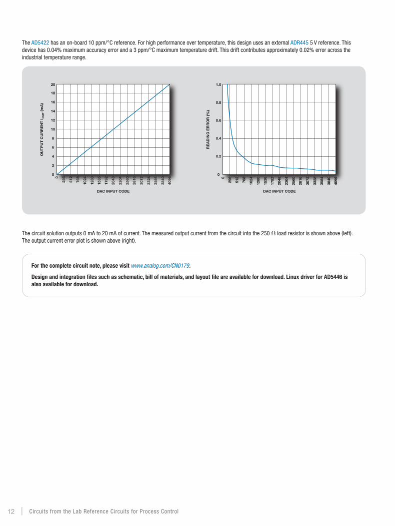
The AD5422 has an on-board 10 ppm/°C reference. For high performance over temperature, this design uses an external ADR445 5 V reference. This device has 0.04% maximum accuracy error and a 3 ppm/°C maximum temperature drift. This drift contributes approximately 0.02% error across the industrial temperature range.
The circuit solution outputs 0 mA to 20 mA of current. The measured output current from the circuit into the 250 Ω load resistor is shown above (left). The output current error plot is shown above (right).
1.0
0.8
0.6
0.4
0.2
0
0
4096
3840
3584
3328
3072
281625
6
512
768
1024
1280
1536
1792
2048
2304
2560
RE
AD
ING
ER
RO
R (%
)
DAC INPUT CODE
20
18
16
14
12
10
8
6
4
2
0
0
4096
3840
3584
3328
3072
281625
6
512
768
1024
1280
1536
1792
2048
2304
2560
OU
TP
UT
CU
RR
EN
T I
OU
T (m
A)
DAC INPUT CODE
For the complete circuit note, please visit www.analog.com/CN0179.
Design and integration files such as schematic, bill of materials, and layout file are available for download. Linux driver for AD5446 is also available for download.
12 | Circuits from the Lab Reference Circuits for Process Control
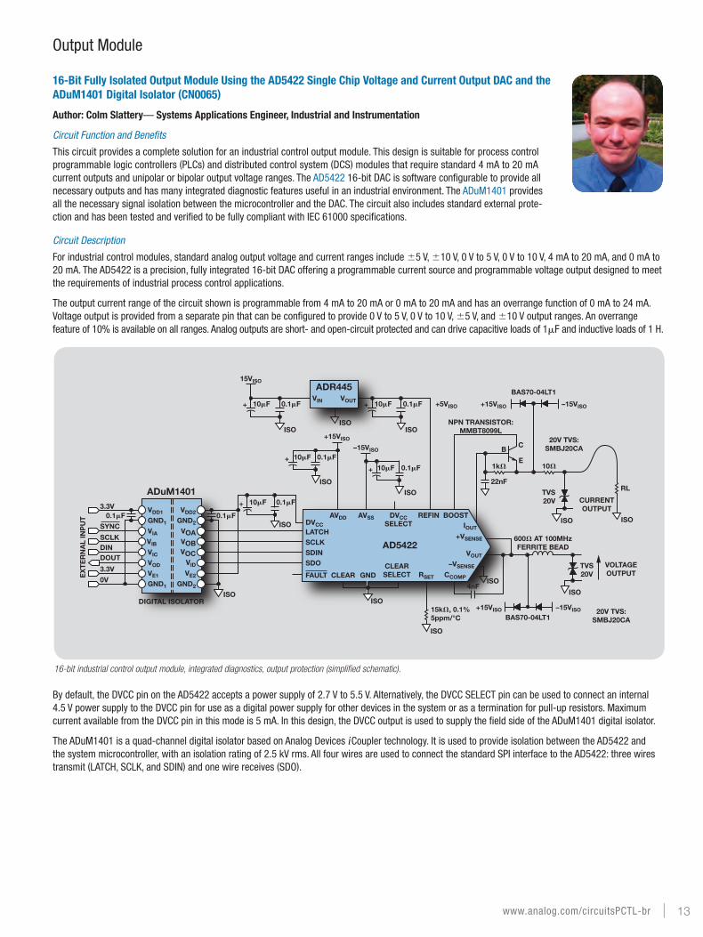
16-Bit Fully Isolated Output Module Using the AD5422 Single Chip Voltage and Current Output DAC and the ADuM1401 Digital Isolator (CN0065)
Author: Colm Slattery— Systems Applications Engineer, Industrial and Instrumentation
Circuit Function and Benefits
This circuit provides a complete solution for an industrial control output module. This design is suitable for process control programmable logic controllers (PLCs) and distributed control system (DCS) modules that require standard 4 mA to 20 mA current outputs and unipolar or bipolar output voltage ranges. The AD5422 16-bit DAC is software configurable to provide all necessary outputs and has many integrated diagnostic features useful in an industrial environment. The ADuM1401 provides all the necessary signal isolation between the microcontroller and the DAC. The circuit also includes standard external prote-ction and has been tested and verified to be fully compliant with IEC 61000 specifications.
Circuit Description
For industrial control modules, standard analog output voltage and current ranges include ±5 V, ±10 V, 0 V to 5 V, 0 V to 10 V, 4 mA to 20 mA, and 0 mA to 20 mA. The AD5422 is a precision, fully integrated 16-bit DAC offering a programmable current source and programmable voltage output designed to meet the requirements of industrial process control applications.
The output current range of the circuit shown is programmable from 4 mA to 20 mA or 0 mA to 20 mA and has an overrange function of 0 mA to 24 mA. Voltage output is provided from a separate pin that can be configured to provide 0 V to 5 V, 0 V to 10 V, ±5 V, and ±10 V output ranges. An overrange feature of 10% is available on all ranges. Analog outputs are short- and open-circuit protected and can drive capacitive loads of 1μF and inductive loads of 1 H.
By default, the DVCC pin on the AD5422 accepts a power supply of 2.7 V to 5.5 V. Alternatively, the DVCC SELECT pin can be used to connect an internal 4.5 V power supply to the DVCC pin for use as a digital power supply for other devices in the system or as a termination for pull-up resistors. Maximum current available from the DVCC pin in this mode is 5 mA. In this design, the DVCC output is used to supply the field side of the ADuM1401 digital isolator.
The ADuM1401 is a quad-channel digital isolator based on Analog Devices iCoupler technology. It is used to provide isolation between the AD5422 and the system microcontroller, with an isolation rating of 2.5 kV rms. All four wires are used to connect the standard SPI interface to the AD5422: three wires transmit (LATCH, SCLK, and SDIN) and one wire receives (SDO).
The ADR125 is a precision, micropower, low dropout (LDO) voltage reference. With an 18 V input voltage, quiescent current is only 95 μA, typical. An LDO voltage reference is preferred because more voltage drop can be tolerated across the loop wires from the control unit to the actuators. The ADR125 requires a small 0.1 μF capacitor at its output for stability. An additional 0.1 μF to 10 μF capacitor in parallel can improve load transient response. Input capacitors, though not required, are recommended. A 1 μF to 10 μF capacitor on the input improves transient response if there is a sudden supply voltage change. An additional 0.1 μF capacitor in parallel also helps reduce noise from the supply.
Bypass capacitors (not shown in figure) are required. In this case, a 10 μF tantalum capacitor in parallel with a 0.1 μF ceramic capacitor should be placed on each power pin of each dual op amp. Details of proper decoupling techniques can be found in Tutorial MT-101 at www.analog.com/MT-101.
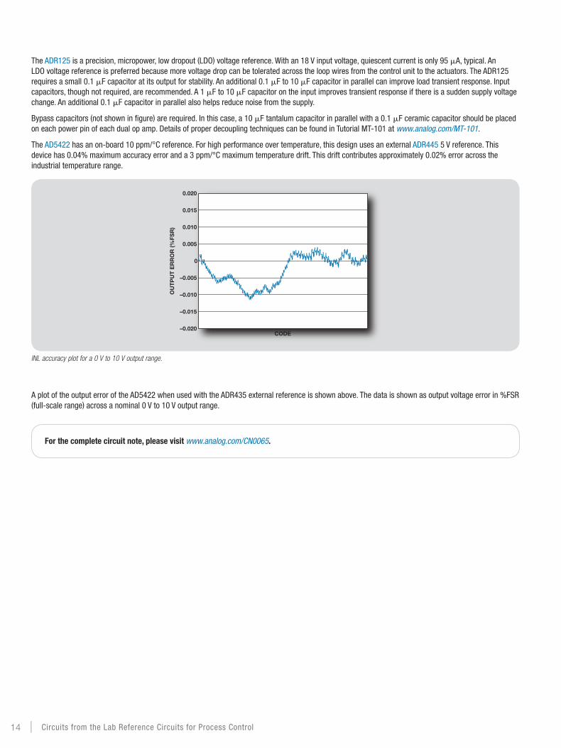
The AD5422 has an on-board 10 ppm/°C reference. For high performance over temperature, this design uses an external ADR445 5 V reference. This device has 0.04% maximum accuracy error and a 3 ppm/°C maximum temperature drift. This drift contributes approximately 0.02% error across the industrial temperature range.
A plot of the output error of the AD5422 when used with the ADR435 external reference is shown above. The data is shown as output voltage error in %FSR (full-scale range) across a nominal 0 V to 10 V output range.
0.020
0.015
0.010
0.005
0
–0.005
–0.010
–0.015
–0.020CODE
OU
TP
UT
ER
RO
R (%
FSR
)
INL accuracy plot for a 0 V to 10 V output range.
For the complete circuit note, please visit www.analog.com/CN0065.
14 | Circuits from the Lab Reference Circuits for Process Control
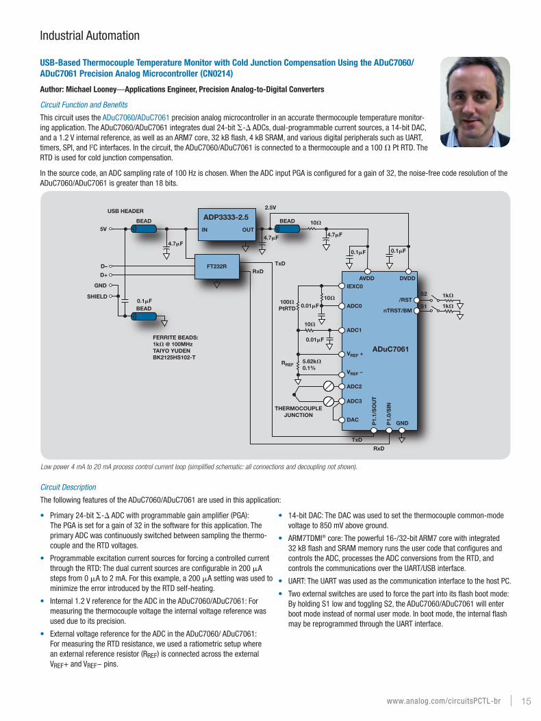
USB-Based Thermocouple Temperature Monitor with Cold Junction Compensation Using the ADuC7060/ADuC7061 Precision Analog Microcontroller (CN0214)
Author: Michael Looney—Applications Engineer, Precision Analog-to-Digital Converters
Circuit Function and Benefits
This circuit uses the ADuC7060/ADuC7061 precision analog microcontroller in an accurate thermocouple temperature monitor-ing application. The ADuC7060/ADuC7061 integrates dual 24-bit Σ-∆ ADCs, dual-programmable current sources, a 14-bit DAC, and a 1.2 V internal reference, as well as an ARM7 core, 32 kB flash, 4 kB SRAM, and various digital peripherals such as UART, timers, SPI, and I2C interfaces. In the circuit, the ADuC7060/ADuC7061 is connected to a thermocouple and a 100 Ω Pt RTD. The RTD is used for cold junction compensation.
In the source code, an ADC sampling rate of 100 Hz is chosen. When the ADC input PGA is configured for a gain of 32, the noise-free code resolution of the ADuC7060/ADuC7061 is greater than 18 bits.
Circuit Description
The following features of the ADuC7060/ADuC7061 are used in this application:
• Primary 24-bit Σ-∆ ADC with programmable gain amplifier (PGA): The PGA is set for a gain of 32 in the software for this application. The primary ADC was continuously switched between sampling the thermo-couple and the RTD voltages.
• Programmable excitation current sources for forcing a controlled current through the RTD: The dual current sources are configurable in 200 µA steps from 0 µA to 2 mA. For this example, a 200 µA setting was used to minimize the error introduced by the RTD self-heating.
• Internal 1.2 V reference for the ADC in the ADuC7060/ADuC7061: For measuring the thermocouple voltage the internal voltage reference was used due to its precision.
• External voltage reference for the ADC in the ADuC7060/ ADuC7061: For measuring the RTD resistance, we used a ratiometric setup where an external reference resistor (RREF) is connected across the external VREF+ and VREF− pins.
• 14-bit DAC: The DAC was used to set the thermocouple common-mode voltage to 850 mV above ground.
• ARM7TDMI® core: The powerful 16-/32-bit ARM7 core with integrated 32 kB flash and SRAM memory runs the user code that configures and controls the ADC, processes the ADC conversions from the RTD, and controls the communications over the UART/USB interface.
• UART: The UART was used as the communication interface to the host PC.
• Two external switches are used to force the part into its flash boot mode: By holding S1 low and toggling S2, the ADuC7060/ADuC7061 will enter boot mode instead of normal user mode. In boot mode, the internal flash may be reprogrammed through the UART interface.
Low power 4 mA to 20 mA process control current loop (simplified schematic: all connections and decoupling not shown).
Both the thermocouple and the RTD generate very small signals; therefore, a PGA is required to amplify those signals. As the auxiliary ADC on the ADuC7060/ADuC7061 does not have a PGA, both were connected to the primary ADC, and switching between the two was done in software.
The thermocouple used in this application is a type T (copper-constantan), which has a temperature range of −200°C to +350°C. Its sensitivity is about 40 μV/°C, which means that the ADC in the bipolar mode with a PGA gain of 32 can cover the entire temperature range of the thermocouple.
The RTD was used for cold junction compensation. The particular one used in this circuit was a platinum 100 Ω RTD, model number Enercorp PCS 1.1503.1. It is available in an 0805 surface-mount package. This RTD has a temperature variation of 0.385 Ω/°C.
Note that the reference resistor, RREF, should be a precision 5.62 kΩ (±0.1%).
The USB interface to the ADuC7060/ADuC7061 is implemented with an FT232R UART to USB transceiver, which converts USB signals directly to the UART. In addition to the decoupling shown, the USB cable itself should have a ferrite bead for added EMI/RFI protection. The ferrite beads used in the circuit were Taiyo Yuden, #BK2125HS102-T, which have an impedance of 1000 Ω at 100 MHz.
The circuit must be constructed on a multilayer PC board with a large area ground plane. Proper layout, grounding, and decoupling techniques must be used to achieve optimum performance.
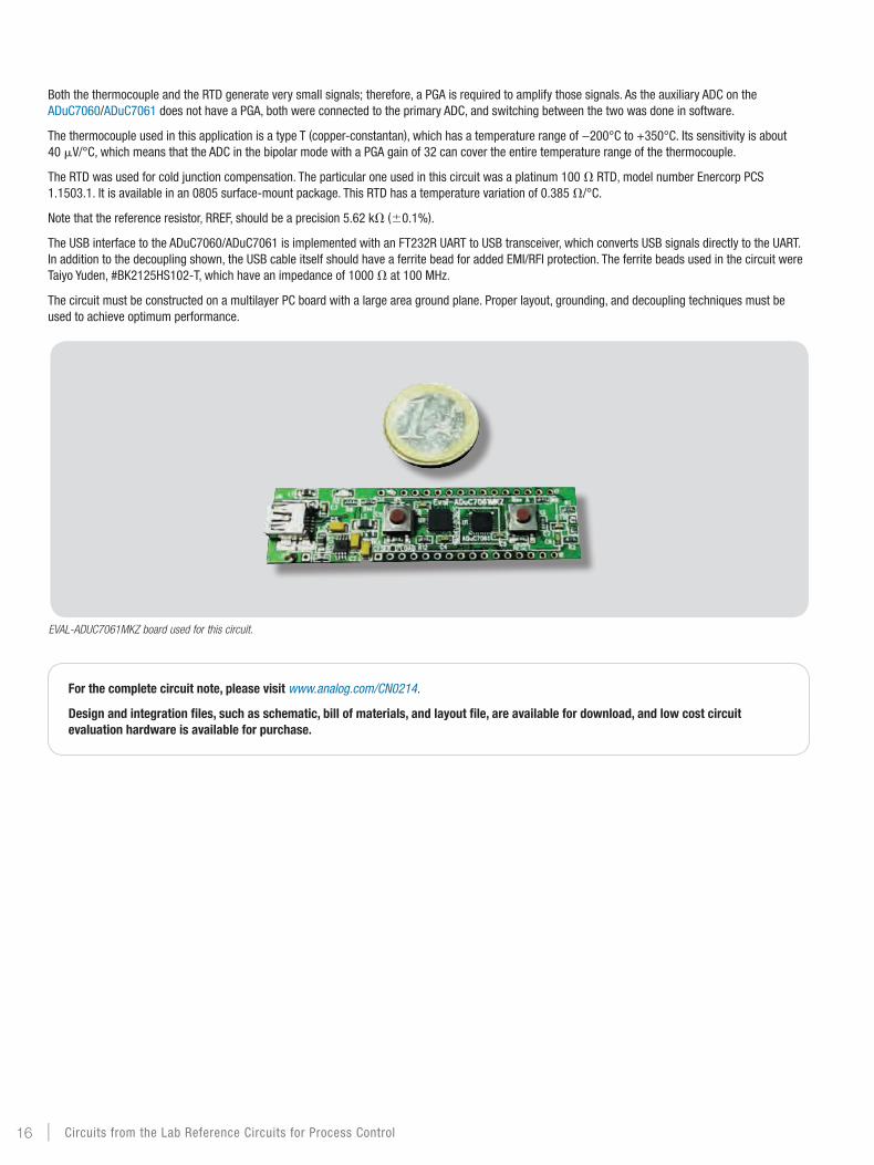
EVAL-ADUC7061MKZ board used for this circuit.
For the complete circuit note, please visit www.analog.com/CN0214.
Design and integration files, such as schematic, bill of materials, and layout file, are available for download, and low cost circuit evaluation hardware is available for purchase.
16 | Circuits from the Lab Reference Circuits for Process Control
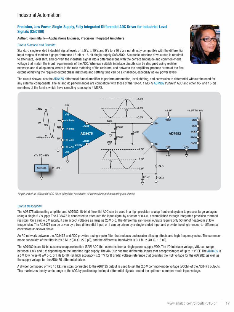
Standard single-ended industrial signal levels of ±5 V, ±10 V, and 0 V to +10 V are not directly compatible with the differential input ranges of modern high performance 16-bit or 18-bit single-supply SAR ADCs. A suitable interface drive circuit is required to attenuate, level shift, and convert the industrial signal into a differential one with the correct amplitude and common-mode voltage that match the input requirements of the ADC. Whereas suitable interface circuits can be designed using resistor networks and dual op amps, errors in the ratio matching of the resistors, and between the amplifiers, produce errors at the final output. Achieving the required output phase matching and settling time can be a challenge, especially at low power levels.
The circuit shown uses the AD8475 differential funnel amplifier to perform attenuation, level shifting, and conversion to differential without the need for any external components. The ac and dc performances are compatible with those of the 18-bit, 1 MSPS AD7982 PulSAR® ADC and other 16- and 18-bit members of the family, which have sampling rates up to 4 MSPS.
Circuit Description
The AD8475 attenuating amplifier and AD7982 18-bit differential ADC can be used in a high precision analog front-end system to process large voltages using a single 5 V supply. The AD8475 is connected to attenuate the input signal by a factor of 0.4×, accomplished through integrated precision trimmed resistors. On a single 5 V supply, it can accept voltages as large as 25 V p-p. The differential rail-to-rail outputs require only 50 mV of headroom at low frequencies. The AD8475 can be driven by a true differential input, or it can be driven by a single-ended input and provide the single-ended-to-differential conversion as shown above.
An RC network between the AD8475 and ADC provides a single-pole filter that reduces undesirable aliasing effects and high frequency noise. The common-mode bandwidth of the filter is 29.5 MHz (20 Ω, 270 pF), and the differential bandwidth is 3.1 MHz (40 Ω, 1.3 nF).
The AD7982 is an 18-bit successive approximation (SAR) ADC that operates from a single power supply, VDD. The I/O interface voltage, VIO, can range between 1.8 V and 5 V, depending on the interface logic supply. The AD7892 has true differential inputs that accept voltages of up to ±VREF. The ADR435 is a 5 V, low noise (8 μV p-p, 0.1 Hz to 10 Hz), high accuracy (±2 mV for B grade) voltage reference that provides the REF voltage for the AD7982, as well as the supply voltage for the AD8475 differential driver.
A divider composed of two 10 kΩ resistors connected to the ADR435 output is used to set the 2.5 V common-mode voltage (VOCM) of the AD8475 outputs. This maximizes the dynamic range of the ADC by positioning the input differential signals around the optimum common-mode input voltage.
Single-ended-to-differential ADC driver (simplified schematic: all connections and decoupling not shown).
This circuit is tested using the AD8475 evaluation board (EVAL-AD8475Z) connected to the Analog Devices PulSAR evaluation board and software. The EVAL-AD8475Z is a customer evaluation board intended to ease standalone testing of AD8475 performance and functionality. The board also enables quick testing with any of the Analog Devices SAR converters—it provides output connectors that mate directly with the analog input connectors (SMB) of the PulSAR evaluation board (EVAL-AD7982CBZ). The ADC converter evaluation and development board (EVAL-CED1Z) connects the setup to a PC through a USB, as shown.
SAR ADC converter evaluation platform (note that the AD8475 differential amplifier evaluation board connects to the SMB analog input connectors of the PulSAR ADC evaluation board).
PC EQUIPPED WITH:
• WINDOWS XP OR WINDOWS 2000
• 1 USB 2.0 SLOT
CONVERTER EVALUATION AND DEVELOPMENT BOARD (EVAL-CEDZ)
• NOT REQUIRED FOR STANDALONE EVALUATION
• COMMON TO MANY ANALOG DEVICES’ ADCs
• SOLD SEPERATELY FROM THE EVALUATION BOARD
• INCLUDES USB CABLES
PULSAR EVALUATION BOARD (EVAL-AD76XX-CBZ)
ANALOG INPUT CONNECTORS (SMB) UNIVERSAL WORLD COMPATIBLE DC POWER SUPPLY (INCLUDED):
INCLUDES ADAPTERS FOR DIFFERENT COUNTRIES
USB 2.0 CABLE
(INCLUDED)
For the complete circuit note, please visit www.analog.com/CN0180.
Design and integration files, such as schematic, bill of materials, and layout file, are available for download, and low cost circuit evaluation hardware is available for purchase.
18 | Circuits from the Lab Reference Circuits for Process Control
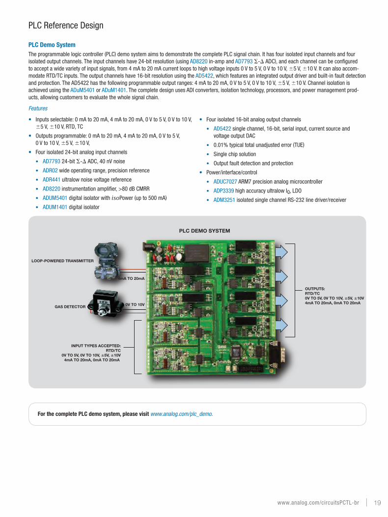
PLC Demo System The programmable logic controller (PLC) demo system aims to demonstrate the complete PLC signal chain. It has four isolated input channels and four isolated output channels. The input channels have 24-bit resolution (using AD8220 in-amp and AD7793 Σ-∆ ADC), and each channel can be configured to accept a wide variety of input signals, from 4 mA to 20 mA current loops to high voltage inputs 0 V to 5 V, 0 V to 10 V, ±5 V, ±10 V. It can also accom-modate RTD/TC inputs. The output channels have 16-bit resolution using the AD5422, which features an integrated output driver and built-in fault detection and protection. The AD5422 has the following programmable output ranges: 4 mA to 20 mA, 0 V to 5 V, 0 V to 10 V, ±5 V, ±10 V. Channel isolation is achieved using the ADuM5401 or ADuM1401. The complete design uses ADI converters, isolation technology, processors, and power management prod-ucts, allowing customers to evaluate the whole signal chain.
Features
• Inputs selectable: 0 mA to 20 mA, 4 mA to 20 mA, 0 V to 5 V, 0 V to 10 V, ±5 V, ±10 V, RTD, TC
• Outputs programmable: 0 mA to 20 mA, 4 mA to 20 mA, 0 V to 5 V, 0 V to 10 V, ±5 V, ±10 V,
• Four isolated 24-bit analog input channels
• AD7793 24-bit Σ-∆ ADC, 40 nV noise
• ADR02 wide operating range, precision reference
• ADR441 ultralow noise voltage reference
• AD8220 instrumentation amplifier, >80 dB CMRR
• ADUM5401 digital isolator with isoPower (up to 500 mA)
• ADUM1401 digital isolator
• Four isolated 16-bit analog output channels
• AD5422 single channel, 16-bit, serial input, current source and voltage output DAC
• 0.01% typical total unadjusted error (TUE)
• Single chip solution
• Output fault detection and protection
• Power/interface/control
• ADUC7027 ARM7 precision analog microcontroller
• ADP3339 high accuracy ultralow IQ, LDO
• ADM3251 isolated single channel RS-232 line driver/receiver
For the complete PLC demo system, please visit www.analog.com/plc_demo.
INPUT TYPES ACCEPTED:RTD/TC
0V TO 5V, 0V TO 10V, ±5V, ±10V4mA TO 20mA, 0mA TO 20mA
0V TO 10V
4mA TO 20mA
LOOP-POWERED TRANSMITTER
GAS DETECTOR
OUTPUTS:RTD/TC0V TO 5V, 0V TO 10V, ±5V, ±10V4mA TO 20mA, 0mA TO 20mA
What Is a Reference Circuit? • Circuit designs that have been built and tested to ensure function and performance.
• Address common analog, RF/IF, and mixed-signal design challenges by applying ADI’s vast applications expertise.
• Thoroughly documented for easy learning, understanding, and integration.
How Is a Reference Circuit Different from a Reference Design?Reference circuits are intended for subsystem level integration, whereas reference designs are typically used as a complete system-level solution. Functioning as a smaller, modular design, a reference circuit can be used as a building block to be integrated in larger systems. Because it is not a standalone system, a reference circuit is more broadly applicable than an application-specific reference design. Also, while reference designs can be expensive, reference circuit documentation and design files are available for free, and some are available with low cost evaluation hardware.
New Enhancements• New reference circuits include
schematics, bill of materials, and layout files.
• Evaluation hardware available for most new circuits.
• Linux device drivers included when applicable.
How to Find a Reference CircuitTo browse the entire collection of circuits, visit www.analog.com/circuits where you can filter and select circuits based on your specific design and desired optimization criteria. Or you may also type the circuit note number directly into the URL: www .analog.com/CNxxxx.
How to Evaluate a Reference CircuitDetailed circuit evaluation, setup, and test informa-tion is included in each circuit note. In some cases, a low cost circuit evaluation board has been developed to enable quick evaluation of the entire circuit. To communicate with the PC via USB 2.0, a controller board may also be available for purchase, as part of the System Demonstration Platform (SDP). This universal evaluation platform provides an easy to use, low cost method for customers to evaluate ADI components and circuits which are SDP-compatible. Once obtained, the SDP can be reused with a variety of ADI product and circuit evaluation boards. For more information on the SDP, please visit www.analog.com/SDP.
To watch an introductory video for Circuits from the Lab, please visit www.analog.com/circuits-video.
For more videos, please visit videos.analog.com.
www.analog.com/circuitsPCTL-br
Analog Devices, Inc.Worldwide HeadquartersAnalog Devices, Inc. One Technology Way P.O. Box 9106 Norwood, MA 02062-9106 U.S.A. Tel: 781.329.4700 (800.262.5643, U.S.A. only) Fax: 781.461.3113
Analog Devices, Inc. Europe HeadquartersAnalog Devices, Inc. Wilhelm-Wagenfeld-Str. 6 80807 Munich Germany Tel: 49.89.76903.0 Fax: 49.89.76903.157
Analog Devices, Inc. Japan HeadquartersAnalog Devices, KK New Pier Takeshiba South Tower Building 1-16-1 Kaigan, Minato-ku, Tokyo, 105-6891 Japan Tel: 813.5402.8200 Fax: 813.5402.1064
Analog Devices, Inc. Southeast Asia HeadquartersAnalog Devices 22/F One Corporate Avenue 222 Hu Bin Road Shanghai, 200021 China Tel: 86.21.2320.8000 Fax: 86.21.2320.8222i2c refers to a communications protocol originally
developed by Philips Semiconductors (now NXP Semiconductors).