115
Helsinki University of Technology Reports in Electron Physics 2001/28 Espoo, October 2001 PROCESSING OF HIGH EFFICIENCY SILICON SOLAR CELLS Jaakko Härkönen

Helsinki University of Technology Reports in Electron Physics 2001/28 Espoo, October 2001
PROCESSING OF HIGH EFFICIENCY SILICON SOLAR CELLS Jaakko Härkönen

Helsinki University of Technology Reports in Electron Physics 2001/28 Espoo, October 2001
PROCESSING OF HIGH EFFICIENCY SILICON SOLAR CELLS Jaakko Härkönen Dissertation for the degree of Doctor of Science in Technology to be presented with due permission for public examination and debate in Auditorium S4 at Helsinki University of Technology on the 9th of November 2001 at 12 o’clock noon. Helsinki University of Technology Department of Electrical and Communications Engineering Electron Physics Laboratory Teknillinen korkeakoulu Sähkö- ja tietoliikennetekniikan osasto Elektronifysiikan laboratorio

Distribution: Helsinki University of Technology Electron Physics Laboratory P.O.Box 3000 FIN-02015 HUT Tel. +358-9-451 2322 Fax. +358-9-451 5008 http://www.hut.fi/Units/Electron/
ISBN 951-22-5680-0 ISSN 0781-4984
Otamedia Oy Espoo 2001

i
HELSINKI UNIVERSITY OF TECHNOLOGY ABSTRACT OF THE
DOCTORAL THESIS
Author: Title: Date:
Jaakko Härkönen Processing of silicon solar cells 20.3.2001 Number of pages: 106
Department: Professorship:
Department of Electrical and Communications Engineering Microelectronics (semiconductor technology) Code: S-69
Supervisor:
Professor Pekka Kuivalainen
Abstract: Fabrication technology of high efficiency silicon solar cells has been studied in this work. Process development work has been carried out since 1997 within a project “Development of high -efficiency low -cost silicon solar cells”, which was funded by TEKES, Fortum Advanced Energy Systems and Okmetic Ltd. Co –operation with photovoltaic research group of Fortum Surface Chemistry has been very close during the project. Target of this project is to demonstrate by low cost processing technologies, the feasibility of the fabrication of solar cells with a conversion efficiency as high as possible. Three different solar cell configurations and their processing technologies are discussed in this content. The solar cells processed by industrially feasible methods on the low cost multicrystalline silicon wafers are the main focus of this work. Solar cells made of single crystalline silicon are studied in order to reveal the capability of the fabrication process in scope of the conversion efficiency. The third cell technology is the devices made by Rapid Thermal Processing of silicon wafers. That topic has been studied because of its possible potential for excellent manufacturability. Processing of the solar cells has been carried out in the clean room facilities of Microelectronics Center at HUT. In addition to device processing, a special issue in this project has been characterization of metallic impurities and defects in multicrystalline silicon material. Minimization of unwanted impurities and defects as well as understanding their interactions is necessary when processing high performance devices. Process induced contamination sources has been charted by µPCD ( microwave Photoconductive Decay ) and SPV ( Surface Photovoltage ) measurements. Other special issues in this thesis are investigation of passivation properties of PECVD grown Si3N4 films, optimization of emitter diffusion and Cr/Cu front contact metallization. During three years, several hundreds of single and multicrystalline silicon wafers have been processed to solar cells. Best conversion efficiencies were 15,1 % ( mc-Si ), 16,4 % ( c-Si ) and 14,5% ( RTP mc-Si ). Keywords:
Solar cells, Multicrystalline silicon, Silicon processing, Lifetime.

ii
Preface I would like to thank professor Juha Sinkkonen for possibility to carry out the research for this work at the Electron Physics Laboratory. Professor Pekka Kuivalainen deserves a big thanks for being my supervisor. This Doctoral Thesis is a result of project which has been funded by TEKES, Fortum Advanced Energy Systems and Okmetic Ltd. I would like to warmly thank these instances for their funding and sympathy for photovoltaic research at the Electron Physics Laboratory. Among the steering group of the project, I would especially like to thank Dr. Emmanuel Fabre and Dr. Tuomo Suntola for many fruitful discussions and advices. The results presented in this work would not have been possible without very close co-operation between the photovoltaic research groups of HUT and Fortum. The co –operation used to be unusual informal, flexible and constructive. In other words, it was a pleasure to make solar cells together with Dr. Pentti Passiniemi, M.Sc. Markko Rajatora and M.Sc. Teemu Marjamäki. The experimental research on the semiconductor devices is a team work. The results to be presented in this work are results of the team. I warmly thank all the members of the photovoltaic research group of the Electron Physics Laboratory that have given their contributions to this work. Especially, it was my privilegde to conduct the research for the Master’s Thesis of Tuuli Juvonen and Kimmo Solehmainen. The results of their studies are referred in Chapters 10 and 11. The process development of semiconductor devices requires a great number of samples to be processed. The clean room work was mostly done by skillfull professionals. I would like to thank the laboratory technicians Janne Kylmäluoma and Helena Karppinen for their very important work that made us possible to demonstrate high efficiency silicon solar cells. M.Sc. Kukka Banzuzi corrected my English which is far away from perfect. I appreciate very much her efforts. I thank my colleagues at the Electron Physics Laboratory for the good athmosphere and “Jenny ja Antti Wihurin säätiö”, “Väisälän säätiö” and “ Ulla Tuomisen säätiö” for the economical support. I would also like to thank my family for the encouragment during my studies. This work is dedicated to memory of my mother. Jaakko Härkönen Geneve 22.03.2001

iii
List of Symbols A Area of the solar cell AFM Atomic Force Microscope AM1.5G Air Mass 1.5 Global ARC Antireflection Coating α Absorption coefficent αν Coefficient of thermal expansion BSF Back Surface Field GaAs Gallium Arsenide C(z) Spatial collection efficiency function of the solar cell σ Capture cross sections CdTe Cadmium Telluride CIS Copper Indium diSelenide DI Deionized water CH3COOH Acetic acid CO2 Carbon dioxide CVD Chemical Vapor phase Deposition Cu Copper Cr Chromium Cz-Si Czochralski silicon Dn,p Diffusion constant of electrons and holes DS Direct solidification d Strain rate E Electric field Ea Activation energy Ei Intrinsic Fermi level E* Young’s modulus eV Electron volt ε Dielectric constant Fe –B Iron boron pair Fz-Si Float Zone silicon F(λ),Φ(λ) Flux of the incident light FF Fill factor G Generation rate HF Hydrofluoric acid Is Diode saturation current Isc Short circuit current IL Light generated current IQE Internal Quantum Efficiency J Current density kB Bolzmann’s constant L Diffusion constants λ Wavelength LBIC Laser Beam Induced Current MWp Mega Watt Peak, nominal output power of the solar cell mc-Si Multicrystalline silicon NaOH Sodium hydroxide NH4OH Nitric acid

iv
NA Acceptor doping density ND Donor doping density Nit Interface trap density ni Intrinsic doping concentration n Concentration of electrons OH- Hydroxide ion Ω Ohm PECVD Plasma Enhanced Chemical Vapour Deposition p Concentration of holes PCD Photoconductivity Decay PC1D Device simulator η Conversion efficiency of the solar cell R Recombination rate R(λ) Reflection coefficent RIE Reactive Ion Etching RTO Rapid Thermal Oxidation ρ Charge density µn,p Mobility of electrons and holes σrr,θθ Thermoelastic stress Sn,p Surface recombination velocity for electrons and holes SC Standard Cleaning SEM Scanning Electron Microscope SF6 Sulphurichexafluoride SiO2 Silicon dioxide SOD Spin –on Dopant SR(λ) Spectral response of the solar cell Si3N4 Silicon Nitride SiNx Non –stoichiometric silicon nitride SPV Surface Photovoltage τ Lifetime τeff Effective lifetime τB Bulk lifetime T Absolute temperature V Voltage Voc Open circuit voltage of the solar cell vth Thermal velocity ν Poisson’s ratio Wscr Width of the space charge region WB Width of the base region WE Thickness of the emitter z,x Distance

v
Contents 1. Introduction 1
2. Physics of pn –junction solar cells 5
3. Lifetime characterization 17
3.1 Photoconductivity Decay ( PCD ) method 18 3.2 Surface Photovoltage measurement 21
4. Efficiency losses 25
5. Multicrystalline silicon 28
6. Wafer cleaning and wet etching 35
7. High temperature processing of solar cells 41
7.1 Lifetime characterization of high temperature processing 49 7.1.1 Experimental procedure 51 8. Antireflection coating 55
8.1 Properties of silicon nitride thin films grown by PECVD 55 8.2 Characterization of PECVD grown Si3N4 57
9. Contacts of solar cells 63 9.1 Processing of the front contact 66 9.2 Processing of the back contact and Back Surface Field ( BSF ) 68 10. Rapid Thermal Processing ( RTP ) of solar cells 71
10.1 Experimental 75
11. Processing of single crystalline silicon solar cells 77
11.1 Substrate technology 77 11.2 Processing of high efficiency single crystalline silicon solar cells 81
12.Characterization of solar cells 87 13. Results 90 13.1 Comparison of measured and simulated parameters 91

vi
14. Conclusions 98 References 103

1
1. Introduction
Environmental awareness has traditionally motivated the research of renewable energy
sources. Solar cells convert sunlight directly to electrical power without any pollution,
exhaust, fuel, noise or moving parts. Benefits of this elegant form of the energy
conversion from cost free solar radiation to the most usable form of the energy, electrical
current, have been recognized decades ago. However, despite of three decades of
intensive research, photovoltaic devices correspond today only to a very small amount of
the global energy production, and it has been widely accepted that solar cells cannot be
implemented as a primary energy source in the industrialized countries. This is mainly
due to the lack of methods to store electricity and the high expenses of solar energy
system components. There can still be, however, a great environmental impact if solar
cells reduce effectively the use of fossil fuels in developing countries, which are
predicted to be responsible for a major part of global CO2 emissions in the future.
Solar energy markets show significant annual growth numbers. Renewable
energies oriented business seems to have reached a certain degree of maturity, i.e.
moving from governmentally subsidized activity towards a truly market steered industry.
Cumulation of installed photovoltaic energy production capacity
0
50
100
150
200
250
300
350
400
1990 1991 1992 1993 1994 1995 1996 1997 1998
Year
MW
p ( n
omin
al p
ower
)
Figure 1. Annual installed PV power according to the Reference [1].
2
Photovoltaic markets clearly have two mainstreams. One is to produce electricity as
cheaply as possible and the other one is to maximize the performance of the solar energy
system at the moderate level of costs. Statistics of the solar energy system production is
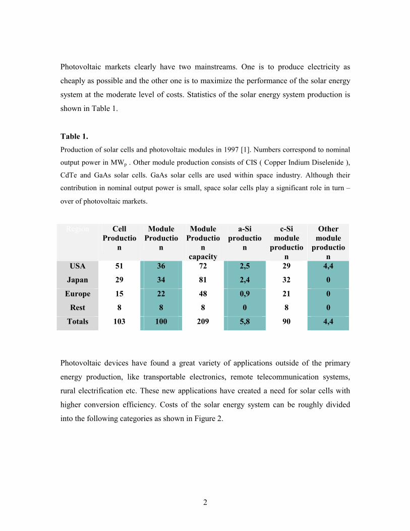
shown in Table 1.
Table 1. Production of solar cells and photovoltaic modules in 1997 [1]. Numbers correspond to nominal
output power in MWp . Other module production consists of CIS ( Copper Indium Diselenide ),
CdTe and GaAs solar cells. GaAs solar cells are used within space industry. Although their
contribution in nominal output power is small, space solar cells play a significant role in turn –
over of photovoltaic markets.
Region Cell Productio
n
Module Productio
n
Module Productio
n capacity
a-Si productio
n
c-Si module
production
Other module
production
USA 51 36 72 2,5 29 4,4
Japan 29 34 81 2,4 32 0
Europe 15 22 48 0,9 21 0
Rest 8 8 8 0 8 0
Totals 103 100 209 5,8 90 4,4
Photovoltaic devices have found a great variety of applications outside of the primary
energy production, like transportable electronics, remote telecommunication systems,
rural electrification etc. These new applications have created a need for solar cells with
higher conversion efficiency. Costs of the solar energy system can be roughly divided
into the following categories as shown in Figure 2.

3
Figure 2. Cost distribution of solar energy system [2].
According to Fig. 2 , about one fifth of the total costs of a photovoltaic module is
attributed to the silicon substrate. One multicrystalline wafer ( 100cm2 ), costed about 1,8
USD in 1999. If a conversion efficiency of 14% is assumed a total number of 37 mc –Si
solar cells are required for a 50 Wp ( nominal output power under AM1.5G illumination
conditions ) module. Total costs of the module would then be 333 USD . According to
the Reference [3], daily solar radiation in Southern Finland in September is about 3
kWh/m2 . The photovoltaic module would therefore produce 3 kWh/m2 * 0,37m2 * 14%
of electrical energy which is about 0,15 kWh. In photovoltaic costs analysis, the lifetime
of solar energy system is usually assumed to be 30 years. If average solar radiation in
September is assumed to be the same as average radiation throughout the year, the
module would produce about 1700 kWh in 30 years. That would lead to a price of 5 USD
/ kWh which is at least 50 times more than the price of electricity in Finland in 1999.
Wide utilization of solar electricity is apparently not economically competitive at
the moment in Finland. It is, however, difficult to predict the future of solar energy from
the global point of view. Obviously most of the world’s population could be regarded as
potential users of photovoltaic energy. It is characteristic that in densely populated areas,
for example India or China, energy consumption per capita is much less than in the
industrialized countries. Also, in these areas the power density of solar radiation is
typically larger by a factor of two compared to Finland. It is definitely not insignificant

4
whether the energy demand in developing areas is fulfilled by burning fossil fuels or by
renewables.
5
2. Physics of pn –junction solar cell
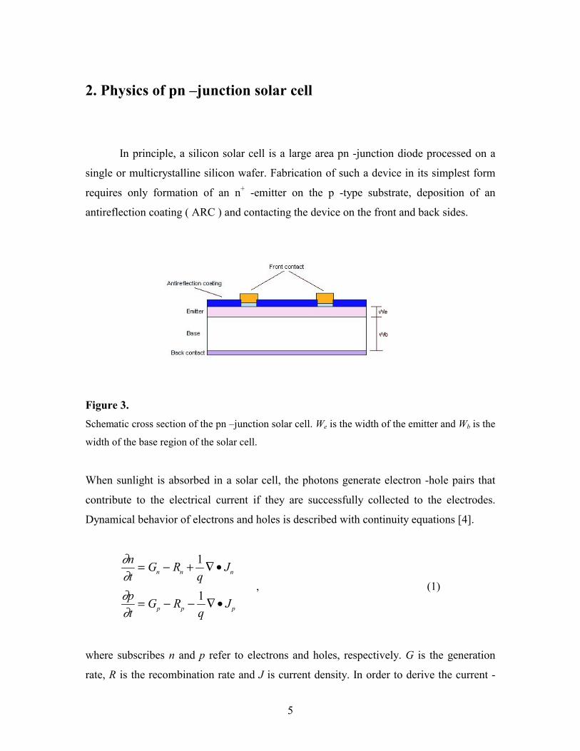
In principle, a silicon solar cell is a large area pn -junction diode processed on a
single or multicrystalline silicon wafer. Fabrication of such a device in its simplest form
requires only formation of an n+ -emitter on the p -type substrate, deposition of an
antireflection coating ( ARC ) and contacting the device on the front and back sides.
Figure 3. Schematic cross section of the pn –junction solar cell. We is the width of the emitter and Wb is the
width of the base region of the solar cell.
When sunlight is absorbed in a solar cell, the photons generate electron -hole pairs that
contribute to the electrical current if they are successfully collected to the electrodes.
Dynamical behavior of electrons and holes is described with continuity equations [4].
∂∂∂∂
nt
G Rq
J
pt
G Rq
J
n n n
p p p
= − + ∇ •
= − − ∇ •
1
1 , (1)
where subscribes n and p refer to electrons and holes, respectively. G is the generation
rate, R is the recombination rate and J is current density. In order to derive the current -
6
voltage relationship of semiconductor devices, three more equations are needed. The
Poisson equation is a special case of the Maxwell's equations when no magnetic field is
present. The Poisson equation gives the relationship between charge density and electric
field.
∇ • =E 1ε
ρ , (2)
where E is the electric field, ε is the dielectric constant of the semiconductor and ρ is the
charge density. Current in a semiconductor device is a result of the flow of electrons and
holes which is caused by the electric field and the gradient of the carrier density.
J q nE qD nJ q nE qD p
n n n
p p p
= + ∇= − ∇
µµ
, (3)
where Dn,p is the diffusion constant of the given semiconductor. The first component of
the current density is the so called drift current and second term is the diffusion current.
The diffusion constant depends on the temperature and mobility of the charge carriers
and can be expressed with the so called Einstein’s relation.
D k Tqn pB
n p, ,= µ , (4)
where µn,p is the mobility of electrons and holes and kB is the Boltzmann’s constant. The
mobility of the charge carriers in silicon is a well -known material parameter and it is
affected by different scattering processes. Schematic illustration of charge carrier
densities in an illuminated pn –junction structure is shown in Figure 4.
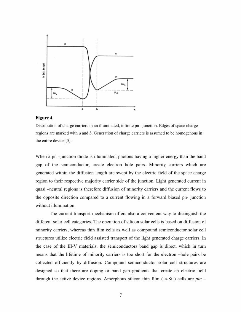
7
Figure 4. Distribution of charge carriers in an illuminated, infinite pn –junction. Edges of space charge
regions are marked with a and b. Generation of charge carriers is assumed to be homogenous in
the entire device [5].
When a pn –junction diode is illuminated, photons having a higher energy than the band
gap of the semiconductor, create electron hole pairs. Minority carriers which are
generated within the diffusion length are swept by the electric field of the space charge
region to their respective majority carrier side of the junction. Light generated current in
quasi –neutral regions is therefore diffusion of minority carriers and the current flows to
the opposite direction compared to a current flowing in a forward biased pn- junction
without illumination.
The current transport mechanism offers also a convenient way to distinguish the
different solar cell categories. The operation of silicon solar cells is based on diffusion of
minority carriers, whereas thin film cells as well as compound semiconductor solar cell
structures utilize electric field assisted transport of the light generated charge carriers. In
the case of the III-V materials, the semiconductors band gap is direct, which in turn
means that the lifetime of minority carriers is too short for the electron –hole pairs be
collected efficiently by diffusion. Compound semiconductor solar cell structures are
designed so that there are doping or band gap gradients that create an electric field
through the active device regions. Amorphous silicon thin film ( a-Si ) cells are pin –
8
diodes where the electron -hole pairs are collected from the intrinsic layer by drift
current. It is possible to make efficient solar cells of materials having a non –orientated
crystallographic structure or a direct band gap, because the absorption of light is
significantly stronger in these material systems. Detrimental high recombination rate can
be circumvented by using the drift current transportation provided by the internal electric
fields that penetrate through the relatively thin device regions.
In a simple analysis of the ideal pn –junction diode, recombination in the space
charge region as well as the drift –current component in Eq (3) are neglected. For
minority carriers in the n- side of the illuminated pn -junction
D d pdx
p G
p p p
pp
n n
2
2
0
∆ ∆
∆
= −
= +
τ , (5)
where τp is the lifetime of holes and pn0 is the minority carrier concentration at the
thermal equilibrium. General solution of this differential equation is
∆p G Ae Bep
xL
xLp p= + +
−
τ , (6)
where Lp is the diffusion constant for holes. The diffusion constant connects diffusion
length to another important parameter, the lifetime, with the following relation
L Dn p n p n p, , ,= τ . (7)
A and B in Eq (6) are constants which are determined from boundary conditions.
Constant A is zero because there must be some finite concentration of holes when x
approaches infinity in the given geometry. In order to find out the constant B, it is
necessary to find out the hole concentration at the edge of the space charge region at the n
–side of the diode which is marked with b in Figure 4. According to [3], concentration of
holes depends exponentially on the voltage across the diode at x=0.
9
p p en b n
qVk T
a
B, = 0 , (8)
where T is temperature, Va is the voltage over the diode and the subscribe b refers to
Figure 4. Solution of Eq (5) with the above mentioned boundary conditions is
p p G p e G en n p n
qVk T
p
xL
a
b p= + + −
−
−
0 0 1τ τ , (9)
If the minority carrier distributions on both sides of the junction are known as in Eq (9),
the total diffusion current can be calculated.
J J J
J xqD p
Le e qGL e
J xqD n
Le e qGL e
tot n p
pp n
p
qVk T
xL
n
xL
nn p
n
qVk T
xL
n
xL
a
B p p
a
B n n
= +
= −
−
= −
−
− −
− −
( )
( )
0
0
1
1
. (10)
The total current density is uniform through the entire diode. In the space charge region
recombination is neglected, but generation is included and it is given by
J qW Gscr scr= , (11)
where Wscr is the width of the space charge region. Current density in the diode can be
obtained by adding the minority carrier current densities at x= 0 to the current density
generated in the space charge region. The relationship between current and voltage in a
solar cell under illumination can be now written as
10
I I e I
I qG L W L
s
qVk T
L
L n scr p
a
B= −
−
= + +
1
( )
, (12)
where Is is a so called diode saturation current which is caused by different recombination
mechanisms. This can be obtained from Eq (10) and it is given by
I A qD nL N
qD nL Ns
n i
n A
p i
p D
= +
2 2
, (13)
where NA is the acceptor doping density, ND is the donor doping density, A is the area of
the solar cell and ni is the intrinsic carrier concentration of silicon given by
kTE
VCi
g
eNNn−
=2 , (14)
where NC,V are the densities of states in the conduction and valence bands, respectively.
Eg is the band gap of the semiconductor in electron volts. It can be seen that there is an
exponential dependence of the intrinsic carrier concentration on the temperature.
Consequently there is a similar dependence of diode saturation current i.e leakage
current. This, in turn, leads to the fact that the conversion efficiency of solar cells is
sensitive to temperature. The problematics related with the temperature dependence is
discussed in Chapter 12 , where the measurement technology of solar cells is described.
Efficiency of a solar cell is the ratio of electrical output power and incident optical
power. It is usually expressed in terms of short circuit current, open circuit voltage and
fill factor.
η = = =
=
PP
I VP
I V FFP
FF I VI V
out
in in
sc oc
in
sc oc
max max
max max
(15)

11
As shown in Eq (22) , fill factor FF is defined to be the ratio between maximum
operation points and short circuit current and open circuit voltage. Fill factor is reduced
by series resistance, leakage current over the edges of the solar cell or leakage current
caused by recombination. The electrical parameters of the solar cell are visualized in a
schematic current-voltage characteristics shown in Figure 5.
Figure 5. Schematic IV –curve of the solar cell under illumination. The parameters Voc , Isc , Vmax and Imax
are defined in Equations (12) and (15) .
The above analysis of the current –voltage characteristic of the illuminated pn –
junction diode is based on a very simple model and several approximations. More
detailed analysis, which takes into account an important device parameter, namely the
surface recombination velocity, is carried out in the Appendixes of Reference [3], and
only the results are presented here. A more realistic picture of solar cell operation is
obtained if the first term on the right hand side in Eq (13) is multiplied by constant FN
and second term is multiplied by FP.

12
F
S WL
DLp
WL
DL
WL
S WL
N
pE
p
p E
p
h
p
E
pp
E
p
=
+
+
cosh( ) sinh( )
cosh( ) sinh( ) , (16)
and
FS W
LDLn
WL
DL
WL
S WL
P
nB
n
n B
n
n
n
B
nn
B
n
=+
+
cosh( ) sinh( )
cosh( ) sinh( ) , (17)
where WB is the width of the base region of the diode i.e. the thickness of the silicon
wafer and WE is the thickness of the emitter as presented in Figure 2. In practice, WB is
several hundreds of micrometers and WE is essentially the same as the depth of the
diffused pn -junction. Sn,p is the surface recombination velocity for electrons and holes,
respectively.
The IL in Eq (12) is current generated by incident light. In addition to carrier
generation rate, it can be also expressed in terms of Spectral Response ( SR ).
( )I Aq SR R F dL = − ( ) ( ) ( )λ λ λ λλ
λ
10
1
, (18)
where A is the area of the solar cell, λ is the wavelength of light, SR(λ) is the spectral
response of the solar cell, F(λ) is the flux of the incident light and R(λ) is the reflection
coefficient of the solar cell. The output current of the solar cell as a function of the
wavelength of light is called spectral response. Internal spectral response can be
expressed with [6]

13
( ) ( ) ( )SR z C z dzα α α= −∞
exp0
, (19)
where α is the absorption coefficient of silicon and it can be expressed in terms of
wavelength of the light, C(z) is spatial collection efficiency function of the solar cell and
z is the distance. The collection efficiency function describes solar cells ability to
generate electrical current from the absorbed sunlight. The function is defined separately
for different regions of the solar cell
( ) ( ) ( )( ) ( )
( )
( ) [ ] [ ]( ) ( )
C zK z L z L
K W L W Lz W
C z W z L W
C zK L z L L z L
K W L W LL W z L
p p p
p E p E pE
E B
n n n
n B n B nB
=+ −
+ −≤ ≤
= ≤ ≤ −
=− + − −
+ −− ≤ ≤
exp / exp /
exp / exp /,
,
exp ( ) / exp ( ) /exp / exp /
, .
0
1 (20)
where Kn and Kp are constants, defined by
KS L DS L Dn p
n p n p n p
n p n p n p,
, , ,
, , ,
//
.=+−
11
(21)
In Equations (12)-(19) there are four parameters that can be influenced by device
processing. These parameters are the reflection properties of the front surface, the
diffusion length in the silicon material, the geometrical dimensions of the solar cell and
the surface recombination velocity.
The open circuit voltage of the solar cell is obtained by setting the current I in
Eq.(12) to zero and solving the voltage.

14
V kTq
IIoc
L
s= +
ln 1 . (22)
This equation implies that the open circuit voltage is determined by logarithmic ratio of
light generated current and diode saturation current. Diffusion length and surface
recombination velocities are present in Equations (12),(13),(15) and (16). These
equations determine the diode saturation current as well as the light generated current.
Therefore in order to maximize the voltage of the solar cell, recombination in the bulk
and at both surfaces need to be minimized. Apparently, an important material parameter
determining the conversion efficiency of the solar cell is the diffusion length in processed
silicon wafer.
As it can be seen in Equations (16) and (17), the dependence of the efficiency on
the lifetime is not linear. Apparently, numerical methods need to be utilized in order to
reveal a reliable prediction of the lifetime versus efficiency relationship. At the given
substrate resistivity, diffusion length is related to the minority carrier lifetime which is a
measure of silicon material quality. Figure 6 presents the simulated dependence between
minority carrier lifetime and conversion efficiency of a solar cell. The simulation has
been carried out with the one -dimensional device simulator PC1D. The relevant
simulation parameters are the same as the ones used for simulation of 15% efficient mc-
Si solar sell in Chapter 12. The parameters are listed in Table 6.

15
Figure 6. Simulated dependence between minority carrier lifetime and conversion efficiency of a solar cell.
It can be seen in Figure 6. that the efficiency of a solar cell is a strong function of the
lifetime in the 1-30µs range. This range of the lifetime, expressed in terms of diffusion
length, corresponds to the thickness of the solar cell or less. Within this range of
deviation, the efficiency varies from 12,7% to 15%. On the other hand, within the range
of lifetime from 30µs to 70µs, the efficiency is improved only about 0,6% and the
increase in the efficiency seems to saturate towards the higher lifetime values. The
conclusion is that, when the diffusion length of the minority carriers approaches the wafer
thickness, the efficiency of the solar cell becomes more and more limited by the
recombination at the back and front surfaces instead of the bulk recombination.
These notifications are fundamentally important when thinking of a low –cost
concept for solar cells. The efficiency gap between world record solar cells and
commercially available cells is about 9-10%. The material as well as the processing cost
can be kept on a reasonable level in scope of solar energy production when a lower class,
i.e. lifetime between 1-30µs, material quality is accepted. It is still possible to achieve a
relatively high efficiency , e.g. 15%. In other words, the production cost can be manifold,
for instance, eight to ten times higher if an efficiency as high as e.g. 16% is urgently
wanted. The challenging task trying to increase the utilization of the solar energy is to
Simulated efficiency vs. bulk lifetime
12
12.5
13
13.5
14
14.5
15
15.5
16
0 10 20 30 40 50 60 70
Lifetime(us)
Effic
ienc
y(%
)
16
push the efficiency of economically produced solar cell up to the limits, near the 15%.
That requires expertise on semiconductor processing technologies and a knowledge of
lifetime behavior in low cost silicon. This work is mainly focused on these topics. Unless
otherwise mentioned, all processes or process recipes, presented in this work are
developed by the author.
17
3. Lifetime characterization
High minority carrier lifetime is the key factor when striving for a good
operational performance of solar cells. Lifetime influences the open circuit voltage, the
short circuit current as well as the fill factor. Despite of the lifetime’s apparent
importance, measurement of the minority carrier lifetime is very seldom straightforward.
In this chapter, two common measurement technologies are shortly presented. A
comprehensive overview of different minority carrier lifetime measurement techniques
and detailed analysis of measurement physics can be found in references [7] and [8] .
Contents of this Chapter is based mainly on these two sources.
Recombination lifetime is a time constant that corresponds to the average decay
time of the excess carriers to be captured by some recombination centers. Recombination
can take place due to impurity atoms in the semiconductors crystal lattice, lattice defects
or surfaces. An excess of minority carriers can be generated by absorption of light or by a
forward biased pn -junction.
All semiconductors contain impurities. As a matter of fact, every foreign atom but
the host atom of the perfect periodic crystal can be considered as an impurity. The
crystallographic point defects and structural defects can be also regarded as impurities.
Impurities can be added to semiconductors in order to change the electrical properties of
the material in different ways, such as diffusion or ion implantation. Doping is a crucial
part of semiconductor processing. On the other hand, a large part of the impurities are
unwanted in the semiconductor material. These impurities are incorporated during the
crystal growth or device processing.
The dopant impurities, usually phosphorous, boron, antimony or arsenide, form so
called shallow -levels to semiconductors band gap. In contrast to dopant atoms, the other
impurities usually form deep -levels to the band gap. In some applications deep -level
impurities are added in a controlled way to the base region of the bipolar devices in order
to decrease the base transit time. Semi -insulating compound semiconductor substrates
are also fabricated by adding some deep -level impurities to the substrate. Excluding
these two applications, deep -level impurities are generally unwanted. In addition to the
18
crystal imperfections, the deep -level impurities in semiconductors include e.g. transition
or refractory metals like copper, iron, gold or chromium. According to the Shockley –
Read –Hall recombination statistics, most efficient recombination centers are the ones
that form deep levels near the mid band gap and have large capture cross sections.
3.1 Photoconductivity Decay ( PCD ) method
In the Photoconductivity Decay method, effective lifetime is measured by
illuminating the wafer by laser pulse, the transient of the decaying minority carrier is
monitored and effective lifetime is extracted from the conductivity transient.
When a silicon wafer is illuminated by monochromatic light having an energy
larger than the band gap, the absorbed photons generate a three dimensional cloud of
electron -hole pairs which decays exponentially within the lifetime.
∆ ∆n t n et
eff( ) ( )=−
0 τ , (23)
where
1 1 2
τ τβ
eff B
D= + , (24)
where τeff is the effective lifetime and τB is the bulk lifetime. Measurement of the
conductive decay therefore gives the value of the effective lifetime. Effective lifetime is a
quantity which depends on the bulk lifetime and parameter β which is defined as
β βtan( )T sD
r
2= , (25)
where D is the so called ambipolar diffusion coefficient and it is given by
19
DD D n pnD pD
n p
n p
=+
+( )
, (26)
and sr is the surface recombination velocity. Surface recombination is caused by the
interruptions in the periodic lattice structure at the end of the wafer or at different silicon /
thin film interfaces which are constantly added to the wafer because of different device
processing purposes. In addition to the interface properties, surface recombination
velocity is also affected by the number of charge carriers in the vicinity of the surface. In
other words, surface recombination velocity is an illumination level dependent quantity.
ss s p n n
s n n n s p p prn p s s s
n s s s p s s s
=+ +
+ + + + +( )
( ) ( )0 0
0 1 0 1
∆∆ ∆
, (27)
where
s v Nn ns th it= σ , (28)
s v Np ps th it= σ , (29)
where σns and σps are capture cross sections of the interface traps, vth is thermal velocity
of charge carriers and Nit is the interface trap density. The n1s and p1s are defined as
n n es i
E EkT
T i
1 =−
, (30)
p n es i
E EkT
T i
1 =−
−
, (31)
where ET is the energy level of the surface trap and Ei is an intrinsic Fermi level. Number
of charge carriers in the vicinity of the surface can be reduced by introducing a depletion
region close to the surface. Silicon surfaces can be depleted for example by certain
20
chemical treatments, corona charging the surface or by providing a fixed charge to a
dielectric film next to the silicon. The latter method is called field-effect passivation.
Commonly used dielectric thin films used in silicon processing are SiO2 and Si3N4 , but
basically all dielectric films have some fixed charge that can be usually tuned by
changing the deposition conditions.
Recombination lifetime of the silicon wafer is a good measure of the material
quality and an important parameter in device modeling of solar cells. Therefore accurate
determination of the bulk lifetime from the PCD measurement data is of special interest.
However, as shown in Eq. (24), the measured lifetime is a combination of bulk lifetime
and a time constant which is determined by surface recombination velocity. There are
only two special cases where bulk lifetime of commercial silicon wafers can easily be
measured with PCD method. This occurs when the bulk lifetime is so short that the
corresponding diffusion length does not exceed the penetration depth of the exciting laser
pulse or when the surface recombination velocity is negligibly small. In the first case, all
the excess carriers have been recombined in the bulk before reaching the front or back
surface of the silicon wafer. The second case is due to the elimination of the surface
recombination, which can only be achieved by very high quality silicon dioxide
passivation that can be obtained by thermal dry oxidation process at high temperatures.
Unfortunately, high temperature processing changes the properties of the silicon wafer
and the measured lifetime is not anymore the original bulk lifetime.
One way to measure lifetimes that give higher diffusion lengths than sample
thickness is to passivate wafer surfaces chemically. In practice, during the PCD
measurement the wafer is placed in a plastic envelope containing a passivation solution.
Iodine in ethanol and HF are commonly used chemical passivators that keep silicon
surfaces terminated by hydrogen. Drawback of the chemical passivation concept is the
questionable stability and reproducibility of this passivation method. Additionally, it can
be inconvenient to return the chemically passivated samples back to a process having
high temperature treatments.
In a lifetime mapping measurement systems, conductivity transient is usually
detected by measuring the reflection of microwave signal. Resistivity of the silicon wafer
must then be more than 1 Ω*cm before PCD measurement can be carried out by

21
commercially available equipment’s. This serious drawback of the PCD method is due to
the detection limits of available microwave antennas and the finite power of exciting
laser pulse.
3.2 Surface Photovoltage measurement
Solar cell substrates have often lower resistivity than 1 Ω*cm. In these cases,
PCD measurements produce lifetime maps which are corrupted by noise because the
amplitude of the conductivity transient is below the detection limit of the measurement
system. In contrast to PCD measurements, Surface Photovoltage (SPV) is a steady state
method which allows the measurement of low resistivity samples.
SPV measurement directly gives a value for the diffusion length. The difference
between injection levels in PCD and SPV are around five to six orders of magnitude.
Many metallic impurities in silicon show some characteristic illumination level behavior.
Therefore the comparison of measurement data obtained by both of these two methods
may give valuable information of the origin of the contamination in solar cells.
If the silicon wafer is continuously illuminated with monochromatic light having
energy larger than band gap, the charge carriers that have diffused to the illuminated
surface are separated by space charge region which is present close to the wafers surface.
The separated carriers create a surface potential VSPV which is within certain limits
linearly proportional to the number of the excess carriers at the space charge regions
edge. The number of the excess carriers at the space charge regions edge can be solved
from the one dimensional continuity equation
D d n xdx
n x G x2
2 0∆ ∆( ) ( ) ( )− + =τ
, (32)
with the boundary conditions determined by surface recombination

22
d n x
dxs n
D∆ ∆( ) ( )= 1
0 at x = 0
(33)
d n x
dxs n t
D∆ ∆( ) ( )= − 2 at x = t .
The generation rate depends on the photon flux of the incident light, the reflectance of the
wafer surface and the wavelength of the light. It is a good assumption that every photon
creates an electron -hole pair. Generation rate in terms of position x and wavelength λ is
then given by
[ ]G x R e x( , ) ( ) ( ) ( )λ λ α λ α λ= − −Φ 1 , (34)
where Φ(λ) is the flux of the incident light. The solution of Eq. 31 with the given
boundary conditions is
∆ Φn x RL
AD
e BD
et t( ) ( )( )
= −−
+ −
− −112 2
1
1
1
1
ατα
α α , (35)
where
A s s LD
s L t xL
s D t xL1
1 22 1= +
−
+ + −
α αsinh ( ) cosh
B s s LD
s L xL
s D xL1
1 21 2= −
+ −
α αsinh ( ) cosh (36)
D s s LD
DL
tL
s s tL1
1 21 2= +
+ +
sinh ( )cosh

23
The Eq. (35) is non -linear and therefore quite impractical for extraction of diffusion
length. However, in order to make successful estimations of the diffusion length only a
linear relationship between the surface photovoltage and the number of excited charge
carriers at the edge of the surface space charge region need to be known. In this analysis,
diffusion length is assumed to be smaller than wafer thickness, and exciting wavelength
is chosen in such a way that the photons are not absorbed within the surface space charge
region nor near of the back side of the wafer. With these assumptions quite complicated
Eq. (35) can be simplified and a linear relationship between surface photovoltage and
carrier concentration can be found.
V C R L
s DL
LSPV
n
n
nn
=−
+ +1
1
11
( )
( )( )
Φ
α
, (37)
where C1 is a constant. Equation (37) is valid for quite restricted values of VSPV. Linear
relationship between the photon flux and surface photovoltage needs to be examined
separately for every sample.
Surface photovoltage is a steady state measurement method. During one SPV
measurement, the surface voltage is kept constant which leaves the photon flux and
absorption coefficient to be the only variables in Eq. 38.
Φ = +
C L2
1α
(38)
where C2 is a constant. When the sample is illuminated by at least two monochromatic
light sources while the surface voltage is kept constant, the diffusion length can be
extracted from interception of the x -axis of the photon flux -absorption coefficient graph
as shown in Fig. 7.
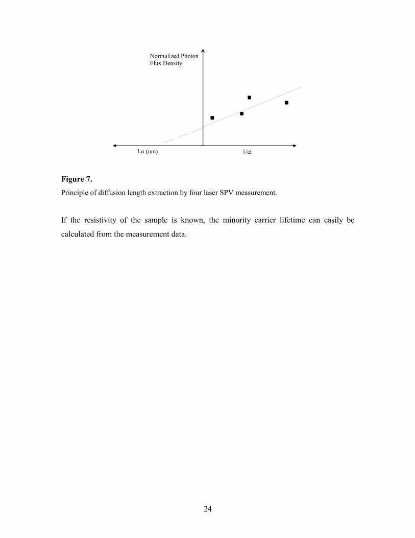
24
Figure 7. Principle of diffusion length extraction by four laser SPV measurement.
If the resistivity of the sample is known, the minority carrier lifetime can easily be
calculated from the measurement data.

25
4. Efficiency losses
In order to experimentally demonstrate high efficiency devices, optical and
electrical losses in silicon material need to be minimized by using semiconductor
processing technologies available. Schematic presentation of the relevant loss mechanism
in solar cells is presented in Figure 8.
Figure 8 Different loss mechanisms in a solar cell [5]. Optical losses in silicon solar cells consist of reflection of light at the front surface of the
solar cell and finite ability of silicon to utilize the radiation spectrum of sunlight. The
latter is caused by the fact that photons having lower energy than silicon’s band gap

26
basically pass through the solar cell. Threshold wavelength of the photons to be absorbed
is 1107 nm.
Figure 9. AM1.5 Global spectrum . The portion of the light that silicon solar cells are able to convert into
electricity is dashed.
Some absorption may also take place at longer wavelengths but its contribution to the
output current is negligibly small. Generation of electron –hole pairs by light having an
energy lower than the band gap requires energy levels to be present between the
conduction and valence bands. Although such levels usually exist in large densities in
non –ideal solar cells, the charge collection properties are so degraded in these cases
badly that sub band gap generation cannot be measured electrically.
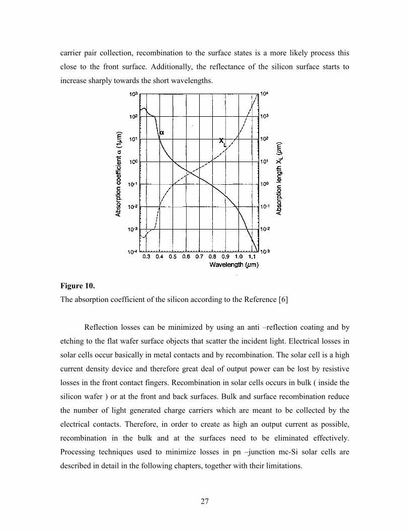
The lowest usable wavelength of light for silicon solar cells is about 350-370nm .
The lower limit is set by the fact that short wavelength photons are absorbed very close to
the front surface. As shown in Figure 10, the absorption length, reciprocal of the
absorption coefficient, is only about 10nm for photons at 370nm. Instead of excited
Am 1.5G spectrum
0
10
20
30
40
50
60
310
340
390
450
510
590
710
762.5
831.5 92
599
3.5 1137
1320
1497
1610
1860
2065
2450
3056
3344
Wavelenght ( nm )
Irrad
ianc
e ( 0
.1W
/ m
^2*n
m )
Air Mass 1.5 Global
Fraction of AM1.5G (370-1120nm)
27
carrier pair collection, recombination to the surface states is a more likely process this
close to the front surface. Additionally, the reflectance of the silicon surface starts to
increase sharply towards the short wavelengths.
Figure 10.
The absorption coefficient of the silicon according to the Reference [6]
Reflection losses can be minimized by using an anti –reflection coating and by
etching to the flat wafer surface objects that scatter the incident light. Electrical losses in
solar cells occur basically in metal contacts and by recombination. The solar cell is a high
current density device and therefore great deal of output power can be lost by resistive
losses in the front contact fingers. Recombination in solar cells occurs in bulk ( inside the
silicon wafer ) or at the front and back surfaces. Bulk and surface recombination reduce
the number of light generated charge carriers which are meant to be collected by the
electrical contacts. Therefore, in order to create as high an output current as possible,
recombination in the bulk and at the surfaces need to be eliminated effectively.
Processing techniques used to minimize losses in pn –junction mc-Si solar cells are
described in detail in the following chapters, together with their limitations.
28
5. Multicrystalline silicon
Multicrystalline silicon ( mc-Si ) wafers consist of single crystalline grains having
different crystallographic orientations separated by grain boundaries. Approximately one
third of the commercial photovoltaic cells are made of mc –Si [9]. Mc –Si has been
predicted in many contents to become the dominant substrate material in the future. That
is mainly due to significantly lower price of the mc-Si compared to the single crystalline
material. Availability of solar grade silicon may also play a crucial role in the future
because the markets of photovoltaic energy systems have been predicted to grow more
than 20% annually. Solar grade silicon has been traditionally fabricated from the "scrap"
of the electronics grade silicon. In order to meet the frequently presented predictions
about solar cell production, there is simply not enough available waste silicon from the
microelectronics industry.
The raw material of the mc –Si and single crystalline silicon ( c-Si ) is basically
similar, semiconductor –grade polysilicon which costs approximately 14-15 USD / kg in
1999 [10]. Mc –Si wafers of 100 cm2 typically cost about ten times less than four inch
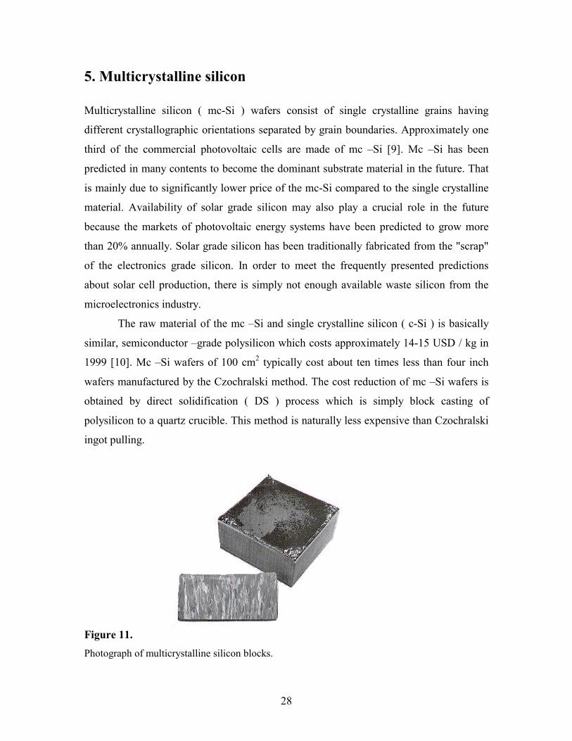
wafers manufactured by the Czochralski method. The cost reduction of mc –Si wafers is
obtained by direct solidification ( DS ) process which is simply block casting of
polysilicon to a quartz crucible. This method is naturally less expensive than Czochralski
ingot pulling.
Figure 11. Photograph of multicrystalline silicon blocks.

29
A desired property of the multicrystalline block is a grain size as large as possible.
Commercially available mc –Si wafers consist of grains that usually are two orders of
magnitude larger than average minority carrier diffusion lengths in grains. The
multicrystalline silicon blocks are cut by wire saw to wafers having thickness of about
300µm. In addition to simple fabrication process, the low price of mc –Si wafers is
consequence of fact that the solar cell substrates do not need to be polished. Schematic
flow chart of mc-Si and Cz-Si wafer processes are shown in Fig 12.
Figure 12. Simple process flow chart of the fabrication sequence of solar cells substrates and silicon wafers
used for microelectronics [11].

30
The cost reduction of the starting material is obtained at the cost of material
quality which has a strong influence on the electrical characteristics of the solar cells.
Concentrations of different impurities in multicrystalline materials are much higher than
in Czochralski silicon, because almost all of the polysilicon raw material, including its
impurities, is transferred to block casts during the solidification. In contrast to direct
solidification, Czochralski process utilizes the advantageous property of silicon melt
enrichment through the impurity segregation during the ingot pulling process. Example of
lifetime distribution in a multicrystalline silicon block is shown in Figure 13.
Figure 13. Example of lifetime distribution in silicon block cast. Picture is from application notes of Semilab
R.T.
It can clearly be seen in Fig 13. that lower lifetime regions are found near the edges of the
ingot. It is obvious that the defected outer edge of the ingot is the result of interaction
between quartz crucible and silicon melt during the solidification. Prior to wafering, the
edge regions are typically removed from the ingot which naturally means lower process
yield. Therefore the optimization of the DS thermal budget and crucible design are
subject of intensive research [11].
Solar cell substrates are boron doped with resistivity of typically 0,5 – 1,0 Ω*cm
which corresponds to doping density of about 1016 cm-3 . Value of base resistivity is a

31
trade off between diffusion length and open circuit voltage and typically needs to be
optimized for each fabrication process. The open circuit voltage increases with
decreasing base resistivity whereas the lifetime tend to decrease drastically when doping
density exceeds 1016 cm-3 . In low cost production of solar cells, the processing is not
carried out in clean rooms and consumption of wet chemicals used for substrate cleaning
is minimized. In such an environment, long diffusion lengths cannot be achieved and
therefore the process is optimized to maximize the open circuit voltage by employing
heavy emitter doping and low base resistivity.
Average µPCD lifetime in non –processed mc-Si wafers is typically about 5µs
which corresponds to about 70µm in diffusion length. Iron has been commonly
recognized to be a lifetime dominant metallic contaminant in solar grade silicon. The
relationship between iron concentration and bulk lifetime has been extensively studied. A
widely accepted experimental relationship between iron concentration and minority
carrier lifetime is presented in Figure 14 [12].
Figure 14.
Experimentally found relationship between iron concentration and µPCD lifetime. 1011cm-3 is the
lowest limit of intentionally introduced iron contamination. Therefore, the influence of iron to
long lifetimes remains therefore to some extent unclear.
32
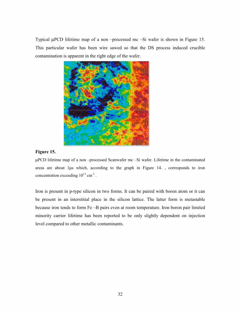
Typical µPCD lifetime map of a non –processed mc –Si wafer is shown in Figure 15.
This particular wafer has been wire sawed so that the DS process induced crucible
contamination is apparent in the right edge of the wafer.
Figure 15.
µPCD lifetime map of a non –processed Scanwafer mc –Si wafer. Lifetime in the contaminated
areas are about 1µs which, according to the graph in Figure 14. , corresponds to iron
concentration exceeding 1013 cm-3 .
Iron is present in p-type silicon in two forms. It can be paired with boron atom or it can
be present in an interstitial place in the silicon lattice. The latter form is metastable
because iron tends to form Fe –B pairs even at room temperature. Iron boron pair limited
minority carrier lifetime has been reported to be only slightly dependent on injection
level compared to other metallic contaminants.

33
Figure 16.
Injection level dependence for different contaminants, according to reference [14]
Injection level dependence similar to Fe-B pairs presented in Figure 17 is found from
SPV and µPCD measurements carried out for the mc-Si wafers used for solar cell
processing.
a) b)
Figure 17.
SPV lifetime map of an unprocessed mc-Si wafer a) and µPCD map of the same wafer. Average
lifetime in the SPV map is 0,9 µs and in the µPCD chart 4,6 µs. The wafer resistivity is about 1
Ω*cm . Therefore the µPCD measurement has been carried out at highest possible injection level
in order to achieve an acceptable signal to noise ratio of the reflected microwave signal.

34
The measurement results presented in the above figure support strongly the conclusion
that the dominant lifetime killer in solar cell substrates is iron.
It is evident that high conversion efficiency cannot be obtained if the diffusion
length in the solar cell is less than 100µm. Lifetime can be improved by correct device
processing. This technique is called gettering which means removing the unwanted
impurities to non -active device regions or outside the substrate. It is well known that a
heavily phosphorous doped layer works as a sink for many metallic impurities in silicon.
At high temperatures metallic impurities diffuse fast in the silicon lattice, but very slowly
in the phosphorous doped regions. Therefore during the emitter diffusion process
unwanted lifetime killers are effectively collected to the emitter region and an increase in
bulk lifetime can be observed by µPCD or SPV measurements.
Figure 18. Cumulative lifetime distributions in mc-Si material after different processing steps. Average
minority carrier lifetime after processing ( n+-diffusion, PECVD silicon nitride deposition,
sputtering and aluminum sintering ) is about 20µs which corresponds to a diffusion length equal
or higher than the thickness of the solar cell.
Cumulative lifetime distribution
0
100
200
300
400
500
600
700
800
900
3 8 13 18 23 28 33 38 43 48
Lifetime (us)
Cou
nts
non -processed
after phosporous diffusion
processd solar cell

35
6. Wafer cleaning and wet etching
In order to obtain a high conversion efficiency, minority carrier lifetime in
multicrystalline silicon wafers must be as high as possible. Bulk lifetime in starting
wafers varies typically from 1µs to 10µs which correspond to diffusion lengths less than
the solar cells thickness. With correct device processing, however, lifetime can be
increased by an order of magnitude, which is mainly due to the phosphorous and
aluminum gettering that automatically occur during the processing. Lifetime
improvement is directly related to the reduction of metallic impurities in silicon.
Concentration of iron in solar grade mc –Si is typically 1011 – 1013 atoms per cubic
centimeter. In other words, less than one part per billion. It is obvious that when
processing solar cells having a high minority carrier lifetime, extreme cleanliness must be
maintained throughout the device processing. Annual worldwide production of silicon
wafers was estimated to be about 10 000 tons in 1992 [15]. For example, one metal coin
would therefore contain enough impurity atoms to contaminate the whole of world’s
silicon production for one year.
The fabrication process described in this thesis has two high temperature furnace
steps, emitter diffusion and aluminum drive –in . Minority carrier lifetime can basically
be degraded during only these two process steps which are carried out at the temperature
high enough for diffusion of solid substances into silicon. Possible sources of unwanted
impurities are naturally numerous, e.g. process equipment, chemicals, DI water, wafer
carriers and wafer handling tools. During device processing, wafer contamination can
never be totally avoided, and proper cleaning process needs to be implemented prior to
the furnace steps. In the fabrication process of mc-Si solar cells, there are three different
mechanism used for wafer cleaning: chemical dissolution of metallic impurities, chemical
oxidation of silicon followed by oxide removal and wet etching of silicon.
The first process step is the anisotropic wet etching of as –cut mc-Si wafers. After
wafering of mc –Si block cast, a damage etching needs to be carried out in order to
remove crystallographic damages which are produced by the wafer saw. Sawing damages
can be as deep as 10µm, and if they are not removed, this results a significant leakage
current. Surface of the wafer is also contaminated by oil and metallic residuals from the

36
wafer saw. Sawing damages, as well as contamination, can effectively be removed
simply by etching enough silicon from both surfaces. During the alkaline etching , OH-
ions provide a significant negative charge to the silicon surface. Cleaning of the wafer
occurs when particles are removed from the surface electrostatically. The principle is
illustrated in Figure 19.
Figure 19. The principle of particle removal during alkaline etching. Picture is from Reference [16].
Damage etching has been carried out by a weak alkaline solution. The etching recipe has
been developed by Fortum Surface Chemistry and it is based on NaOH –isopropanol – DI
water solution. In this etching procedure only a few micrometers of silicon is removed
from the wafer surfaces at a relatively low etching rate. This results in randomized
pyramids to be created in the grains which have (100) or (111) crystal orientations. About
30 – 40 % of the wafer surface becomes effectively textured. SEM picture of randomized
pyramids created by NaOH texturation is shown in Figure 20.

37
Figure 20.
NaOH wet etch textured mc-Si surface.
In addition to surface texturation, significant cost savings are obtained if an alkaline
damage etch is used instead of an acidic etch. Solution containing HF , HNO3 and
CH3COOH is usually called as "acid etchant". Acid etchant planarizes the silicon surface
and it generally results in lower surface recombination velocities, but unfortunately it is
also about ten times more expensive than alkaline based solutions [17] .
After the damage etch and prior to the emitter diffusion mc-Si wafers need to be
cleaned, because the sodium containing etch solution is an extremely harmful
contaminant itself. Sodium is a slow diffusant in silicon and silicon dioxide if compared
to trace metals ( Cu, Ni, Cr, Zn, Au etc ). It means that in addition to reduced lifetime,
once the alkaline metals have entered for example into the quartz parts of the diffusion
system they are difficult to get rid of by any cleaning or gettering process. A RCA
cleaning process is carried out on regular basis before the first high temperature process
step in order to remove alkaline residuals left from the damage etching as well as trace
metals which are probably still present in harmful quantities on the wafer surface. RCA
cleaning, also known as Standard Cleaning ( SC ), has been widely used in
semiconductor industry for more than twenty years. RCA cleaning consists of three steps
and it is carried out in the heated quartz containers. There are many versions of RCA
cleaning. The following recipe has been used at the Electron Physics Laboratory.

38
RCA 1:
6 l DI water
1,2 l NH4OH
1,2 l H2O2
800C / 10min
DI water rinse 10min
HF-dip:
3.5 l DI-water
70 ml HF (aqueous 50%)
RT / 30s
DI water rinse 10min
RCA 2:
6,2 l DI water
1,1 l HCl
1,1 l H2O2
800C / 15min
DI water rinse 10min
RCA 1 clean removes organic contamination and dissolves particles by chemical
oxidation of the silicon. It is important to remove any organic contamination in the
beginning of the cleaning cycle, because some types of organic contamination cause
incomplete oxidation of silicon and therefore lead to partial contamination. In a RCA 1
bath, hydrogen peroxide acts as an oxidizing agent and OH- ions from NH4OH leave a
negative surface charge which repulses particles [18]. Some ion exchange processes
between metals and ammonia can also take place during RCA 1. For example, RCA 1 has

39
been reported to remove copper contamination effectively [19] . The principle of the
particle removal by chemical oxidation is presented in Figure 21.
Figure 21. Particle removal by chemical oxidation.
Next, chemical oxide formed during RCA 1 is removed by a short HF dip. After rinsing
in DI water, the wafers are placed in RCA 2 bath. Cleaning mechanism of RCA 2 is
based on Cl- ions which form volatile metal chlorides that are desorbed from the wafer
surface.
After cleaning, the wafers are ready for emitter diffusion which is described in
Chapter 7. Spin –on Dopant ( SOD ) is basically phosphorous doped silicon dioxide
dissolved in liquid, but despite of baking the SOD at 1200C for 30 minutes, all organic
solvents that are incorporated into the SOD for adjusting the viscosity are not totally
evaporated. During the high temperature treatment, organic residuals adhere strongly to
the silicon surface and as a result, the SOD is very difficult to remove after the diffusion.
Most of the SOD is first removed by buffered HF ( BHF ) which is typically aqueous
NH4F ( 40% ) and HF ( 49% ) with a ratio of 7:1 [16]. Buffered HF removes silicon
dioxide at the rate of about 100nm / min, but does not etch any organic residuals. The
duration of the BHF treatment depends on the thickness of the SOD layer and flatness of
the surface. Removal of spinned SOD from a planar ( acid etched ) mc-Si surface takes
about 10 minutes, whereas sprayed SOD removal from a textured surface may take up to
one hour. Optical microscope picture of SOD residuals is shown in Figure 22.

40
Figure 22. Figure of phosphorous glass residuals on mc-Si wafer. Wafer has been coated with silicon nitride
in order to make the residuals visible. Glass residuals can be seen as bright areas.
The spin –on glass residuals, presented in the figure above, are unacceptable because they
shadow light, prevent contact formation and increase leakage current significantly. RCA
1 clean is an effective method for SOD residual removal, because of its ability to strip
away organic contamination. Hydroxide ions, however, provide a negative surface
potential which is unfortunately opposite to what is needed for field effect passivation of
solar cells. Therefore the SOD removal is finished with a RCA 2 clean.
An alternative method for SOD stripping is oxygen plasma treatment. Plasma
stripping can, however, cause some surface damage because of ion bombardment. Glass
residuals are typically very undefined structures which may create reproducibility
problems in terms of the RIE macro loading effect.
41
7. High temperature processing of solar cells
Fabrication process of multicrystalline silicon solar cells described in this thesis
contains two high temperature furnace steps. The first furnace step is carried out in order
to create a phosphorous doped emitter and the second one is needed for sintering
sputtered aluminum to the back side of solar cells. Emitter diffusion process plays a
crucial role determining the conversion efficiency mainly because of the following
reasons: first, if the emitter doping is too low, good front ohmic contacts are not formed.
This is especially true in the case of screen printed solar cells which require a
phosphorous concentration in the emitter region well above of 1020 cm-3 to achieve a
contact resistance between silicon and thick film paste which is acceptably low.
Additionally, an important component of the series resistance of a solar cell is caused by
the lateral carrier flow in the emitter region. Naturally it depends on the distance between
the contact fingers and on the sheet resistance of the emitter which is in turn a function of
the doping concentration and depth of the diffusion. Effects caused by lateral carrier flow
in the emitter region are very difficult to predict because of lack of two dimensional
modeling tools. Optimization of the emitter diffusion gets even more difficult if the front
surface is textured. On the other hand, too high a concentration of phosphorous leads to
many unwanted effects, such as an increased photon absorption near the front surface due
to band gap narrowing.
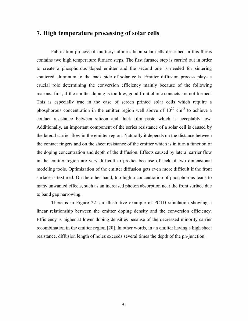
There is in Figure 22. an illustrative example of PC1D simulation showing a
linear relationship between the emitter doping density and the conversion efficiency.
Efficiency is higher at lower doping densities because of the decreased minority carrier
recombination in the emitter region [20]. In other words, in an emitter having a high sheet
resistance, diffusion length of holes exceeds several times the depth of the pn-junction.
42
Figure 23. One dimensional simulation of conversion efficiency dependence on emitter doping density.
Increased resistive losses which occur at the lower doping densities are neglected from this
simulation.
Phosphorous atoms can be transported to silicon wafers in gaseous or in liquid phase. Gas
phase diffusion is carried out in quartz tube furnaces by leading phosphine or
phosphorous oxycloride to the furnace tube. An alternative method is to use solid
phosphorous source wafers which are stacked between the silicon wafers. At high
temperatures phosphorous is transported to silicon wafers with the help of inert carrier
gas. The advantage of gas phase diffusion is the homogeneous doping profile it gives, and
the cleanliness of the diffusion sources compared to the liquid phase diffusion. In a tube
furnace, filled with a gas containing phosphorous, doping takes place on both sides of the
wafers resulting in a parasitic npn –structure. Parasitic junction on the back side of the
solar cell can be tolerated under some circumstances. First, an appropriate edge isolation
needs to be applied in order to prevent the pn –junction to be shunted to the back contact
of the solar cell. Edge isolation can be carried out simultaneously for a large number of
eff iciency vs emitter doping concentration
10
11
12
13
14
15
16
17
18
1,0E+19 6,0E+19 1,1E+20 1,6E+20 2,1E+20 2,6E+20 3,1E+20 3,6E+20 4,1E+20 4,6E+20 5,1E+20
Emitter peak doping density 1/cm^3
effic
ienc
y %

43
solar cells by plasma etching. Solar cells are stacked tightly against each other in a
vacuum chamber, and a couple of micrometers of silicon is etched in fluorine containing
plasma. The parasitic pn –junction on the back side is punched through by sintering or
alloying aluminum. There is currently at least one commercial manufacturer who uses a
fabrication process based on combination of gas phase diffusion of both sides of the solar
cells and edge isolation [21]. Floating junction passivation of the rear side of the solar
cell is a novel application of parasitic phosphorous diffusion. However, this concept
requires photolithography and is therefore excluded from commercial production. A
detailed description of this device concept is given in Reference [22]
In the scope of processing low cost photovoltaic devices, use of liquid phase
dopant sources is more common than gas phase diffusion. All of the solar cells described
in this thesis have been diffused by using Spin-on –Dopant ( SOD ) sources. Diffusion of
solid material in silicon lattice can be described by one dimensional differential equation
which is known as Fick's second law.
∂∂
∂∂
N x tt
D N x tx
( , ) ( , )=2
2 (39)
Where N(x,t) is the concentration of thediffusant as a function of time and position, and D
is the diffusion constant which depends strongly on temperature and to some extent on
the concentration of diffusing species.
D D eEkT
a
=−
0 (40)
Where Ea is the activation energy and D0 is a constant. D0 and Ea are characteristic for
each diffusing species and host material. Since the dopant source in the case of mc-Si
solar cells is a relatively thick phosphorous doped silicon dioxide glass layer, the surface
concentration of phosphorous, Ns can be assumed to be constant during the diffusion. In
this case, the solution of Fick's second law takes the following form.

44
N x t N e ds
xDt
( , ) = −
−1 2 2
0
2
παα (41)
The bracketed expression above is the so called complementary error function and it can
be appreviated by letters.
N x t N erfc xDts( , ) =
2 (42)
In practical case, however, phosphorous diffusion does not follow this simple model
accurately. This phenomena has been extensively studied and it has been explained to be
a consequence of concentration dependence of the diffusion coefficient. With high
phosphorous concentrations, the diffusion coefficient increases rapidly [23].
Emitter diffusion with SOD is carried out in the temperature range from 8400C to
8700C. Sheet resistivities of the mc-Si solar cells are typically varied from 30 Ω⁄ sqr to
100 Ω⁄ sqr, yielding diffusion times at the peak temperature from 30 min to 60min.
Figure 23 shows simulated ( ICECREM process simulator ) diffusion profiles of typical
solar cells emitters.

45
Figure 24. Simulated diffusion profiles when a diffusion source has been a 1021 cm-3 phosphorous doped
silicon dioxide film. Curves represent from left to right 8400C / 35min , 8400C / 60min and 8700C
/ 60min. Simulated thermal cycle starts at 7500C and it is followed by a ramp up with a rate of
150C / min. Cooling is simulated to occur at a rate of 50C / min.
The spin –on dopant used in this process has been supplied by Filmtronics Inc. The
concentration of phosphorous in SOD ( product code P509 ) is 2,0 *1021 cm-3 . Prior to
the diffusion SOD is spinned or sprayed on the RCA cleaned mc –Si wafers. Spraying is
the preferred deposition method because of better step coverage on textured wafers. It is
also very difficult to spin films on the square substrates without special equipment. Some
portion of the rear of the wafer tend to be coated while corners on the front side may
remain partially uncoated resulting a leaking pn –junction. Harmful drawback of the
spray technique is the slightly acidic nature of the SOD which may corrode metallic parts
of the spray equipment. After SOD coating wafers are baked in an air convection oven
for 30min at 1200C . During the baking, liquid solvents in SOD are evaporated and SOD
takes the form of a solid film. The temperature profiles of the furnace recipes used in this
work are summarized in Table 2.

46
Table 2. The diffusion profiles and corresponding recipe names used in this work.
Diffusion/Al-
sintering recipes
Push in T 0C
Ramp up rate. 0C
Peak T 0C
Ramp down rate 0C/min
Pull out T 0C
D2GET
750 8 860 1) 20C/min(→→→→8000
C) 2) 10C/min(→→→→7000
C)
700
D3GET
750 8 850 3) 20C/min(→→→→8000
C) 4) 10C/min(→→→→7000
C)
700
D4GET
750 8 870 5) 20C/min(→→→→8000
C) 6) 10C/min(→→→→7000
C)
700
DTUULI 750 8 820 7) 30C/min(→→→→8000
C) 8) 20C/min(→→→→7000
C)
700
SCAL1
300 10 550 3 0C/min
400
BSF800 (in 4% H2 in N2 )
450 8 800 3 0C/min
450
Wafers were pushed in to tube furnace at 7500C. Diameter of quartz tube is 135mm and
therefore 100cm2 square wafers had to be stacked perpendicular to the quartz tube.
Special quartz boats were designed for this purpose. Temperature was ramped up at the
rate of 150C/min. Ramp rate during the cooling phase has been much slower because of
large thermal mass of the diffusion furnaces. Fastest possible cooling rate is about 3-40C /
min. After diffusions, the sheet resistances of the diffused wafers were checked on a
regular basis with four point probe measurements. Figure 25. shows the sheet resistance
distribution of a heavily phosphorous doped mc-Si wafer.

47
Figure 25. Sheet resistance distribution of diffused mc-Si wafer. Average sheet resistance is 27 Ohm/ sqr,
the minimum is 25 Ohm/ sqr and the maximum is 28 Ohm/ sqr. The sheet resistance scan has
been taken from 78mm diameter circular area from wafer center, although the wafer is 100mm x
100mm square. The measurement has been performed by Tarja Rahikainen at Micro Analog
Systems Ltd.
Figure 26. shows a measured diffusion profile.

48
Figure 26. The diffusion profile measured by spreading resistance equipment. The sample has been diffused
by Filmtronics P509 SOD in a resistively heated belt carrier furnace. The temperature profile has
been essentially the same as in tube furnaces at the Electron Physics Laboratory. Temperature has
first been ramped up rapidly to 8600C and the cooled down at rate of about 20C/min. Resulting
sheet resistance has been 60 –65 Ω / sqr. Measurement data has been supplied by Fortum Surface
Chemistry.
The diffusion profile presented above has been measured from the test sample which is a
polished (100) orientated single crystalline silicon wafer having a base resistivity of 3-7
Ω*cm. Spreading resistance measurement is a spatially resolved four point probe
resistivity measurement. Prior to the measurement the sample needs to be cleaved so that
there is a certain well -known angle within couple of millimeters. Measurement system
steps the probe heads along this cleaved angle and registers values of sheet resistance.
Spreading resistance measurement is possible only for polished samples. Surface
roughness of mc-Si wafers would lead to unmeaningfull measurement results because of
the undetermined start point of the cleaved angle.
49
Comparing the measured and simulated diffusion profiles, it can be observed that the
depths of the pn –junctions are consistent within a reasonable accuracy. On the other
hand, the measured maximum concentration of phosphorous is about an order of
magnitude different from the simulated one. The spreading resistance measurement
shows a peak concentration of about 2*1020 cm-3 , while the computer simulation predicts
that the doping concentration near the surface should be the same as in a SOD layer
which is in Filmtronics P509 2*1021 cm-3 . This is due to a so called "dead layer" effect.
If the concentration of phosphorous exceeds the limit of solid solubility in silicon at the
given diffusion temperature, the excess phosphorous will not be electrically active donor
atoms. Excess phosphorous tends to form precipitates that effectively reduce the solar
cells collection probability near the front surface [24], reducing the conversion efficiency
by about 10 % [25].
7.1 Lifetime characterization of high temperature processing
The minority carrier lifetime in an as –grown, low –cost multicrystalline wafers is
typically only in the range of some microseconds. It is obvious that high efficiency
devices cannot be processed from starting material with such a high concentration of
electrically active impurities and defects, unless lifetime is increased during the
processing.
The “low –cost” fabrication process of pn –junction multicrystalline silicon solar
cells described in this work includes one dopant diffusion and heat treatment of the
metallized wafer. These process steps are known to getter metallic impurities from the
base of the pn –junction diode devices. Especially, phosphorous gettering is a well
established method for reducing the concentration of transition metals in the bulk of the
silicon. Gettering efficiency of phosphorous is also known to increase as function of
concentration of gettering species. Heavily n –doped emitters realized by of phosphorous
diffusion are preferred in practically every commercial mc-Si solar cell configurations.
Phosphorous concentration exceeding 1020 cm-3 ensures low contact resistance of the
screen printed front contacts, small series resistance caused by lateral carrier flow in the
50
emitter and high open circuit voltage of the solar cell. Current gain of the solar cell,
however, shows an opposite behavior as a function of the emitter doping. That is caused
mainly by heavy doping effects described in previous Chapter and by the fact that the
short wavelength collection probability of solar cells is drastically reduced as the pn –
junction penetrates deeper into the base region. Conversion efficiency of the solar cell is
therefore very sensitive to the properties of the phosphorus diffused emitter and typically
the full benefit of gettering cannot be implemented as a part of industrial fabrication
processes.
In this content an experimental evidence of a method which combines emitter
diffusion and a significant enhancement of the minority carrier lifetime in commercially
available multicrystalline silicon wafers is presented. In this experiment minority carrier
lifetime behavior in two groups of multicrystalline silicon wafers, made by the Direct
Solidification ( DS ) method, is investigated. The wafers are made by the same
manufacturer but they are sawed from different ingots. The first group ( class A ), is from
high quality starting material. The base resistivity of class A material is 2,0 Ω*cm and the
average minority carrier lifetime in as –grown wafers is about 10µs. Processed from class
A substrates 100 cm2 solar cells gives conversion efficiencies that clearly exceeds 14%
[24]. The second group of wafers ( class B ) has base resistivity from 0,5 - 1,5 Ω*cm
depending on the position in the ingot. Class B wafers do not meet the wafer
manufacturer's product specifications which guarantee average minority carrier lifetime
to be at least 2µs. This kind of substrate can be considered to be scrap. The solar cells
processed from class B wafers exhibited efficiencies lower than class A cells, typically
between 12 – 13% .
The as –cut wafers are first damage etched and partially textured by a NaOH –
based wet etch which is described in detail in Chapter 6 . Sodium contamination is
removed by an HCl dip followed by RCA clean. Also in this experiment, Spin –On
Dopant has been used for the diffusion source. Filmtronics P509 SOD is deposited onto
wafers and baked 30 minutes at 1200C. Diffusion has been carried out in quartz tube
furnaces with the following temperature profile; push in at 7000C , ramp up to 8700C at
80C / min followed by immediate ramp down to 7000C at 3 0C/min.
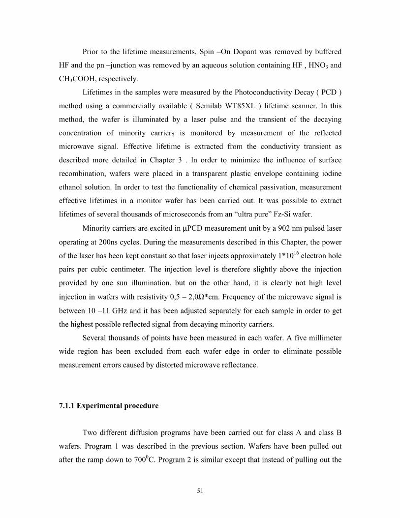
51
Prior to the lifetime measurements, Spin –On Dopant was removed by buffered
HF and the pn –junction was removed by an aqueous solution containing HF , HNO3 and
CH3COOH, respectively.
Lifetimes in the samples were measured by the Photoconductivity Decay ( PCD )
method using a commercially available ( Semilab WT85XL ) lifetime scanner. In this
method, the wafer is illuminated by a laser pulse and the transient of the decaying
concentration of minority carriers is monitored by measurement of the reflected
microwave signal. Effective lifetime is extracted from the conductivity transient as
described more detailed in Chapter 3 . In order to minimize the influence of surface
recombination, wafers were placed in a transparent plastic envelope containing iodine
ethanol solution. In order to test the functionality of chemical passivation, measurement
effective lifetimes in a monitor wafer has been carried out. It was possible to extract
lifetimes of several thousands of microseconds from an “ultra pure” Fz-Si wafer.
Minority carriers are excited in µPCD measurement unit by a 902 nm pulsed laser
operating at 200ns cycles. During the measurements described in this Chapter, the power
of the laser has been kept constant so that laser injects approximately 1*1016 electron hole
pairs per cubic centimeter. The injection level is therefore slightly above the injection
provided by one sun illumination, but on the other hand, it is clearly not high level
injection in wafers with resistivity 0,5 – 2,0Ω*cm. Frequency of the microwave signal is
between 10 –11 GHz and it has been adjusted separately for each sample in order to get
the highest possible reflected signal from decaying minority carriers.
Several thousands of points have been measured in each wafer. A five millimeter
wide region has been excluded from each wafer edge in order to eliminate possible
measurement errors caused by distorted microwave reflectance.
7.1.1 Experimental procedure
Two different diffusion programs have been carried out for class A and class B
wafers. Program 1 was described in the previous section. Wafers have been pulled out
after the ramp down to 7000C. Program 2 is similar except that instead of pulling out the

52
wafers, the process was continued at constant temperature for a relatively long time. A
low temperature is chosen so that phosphorous does not diffuse essentially deeper into
the silicon. In this study, wafers were kept 14 hours at 7000C. Important device design
parameters, emitter sheet resistance and junction depth, remain virtually unchanged as
shown in Figure 27.
Simulated diffusion profile
1.0E+16
1.0E+17
1.0E+18
1.0E+19
1.0E+20
1.0E+21
0 0.2 0.4 0.6 0.8Distance (um)
Con
cent
ratio
n
Diffusion + 14hannealDiffusion
Base doping
Figure 27. Simulated diffusion profiles; a) temperature profile described in previous section b) same
temperature profile followed by 14 hours soak at 7000C. Simulations have been carrier out with
ICECREM process simulator.
According to the simulations, 14 hours heat treatment reduces sheet resistance from 56,7
Ω/sqr to 55,0 Ω/sqr.
In multicrystalline silicon, extended defects like grain boundaries and dislocations
offer preferred sites for precipitation of metallic impurities. Electrical activity of these
defects is known to be strongly dependent on impurities [25], [26]. High temperature
annealing is needed in order to release significant amount of these precipitated impurities.
After cooling down to 7000C, however, many released lifetime killers still have a
significant diffusion velocity and gettering may take place assisted by a large segregation
coefficient between phosphorous doped emitter and moderately boron doped bulk. The
principle of this gettering process as well as detailed theoretical analysis has been
presented in Ref [24].
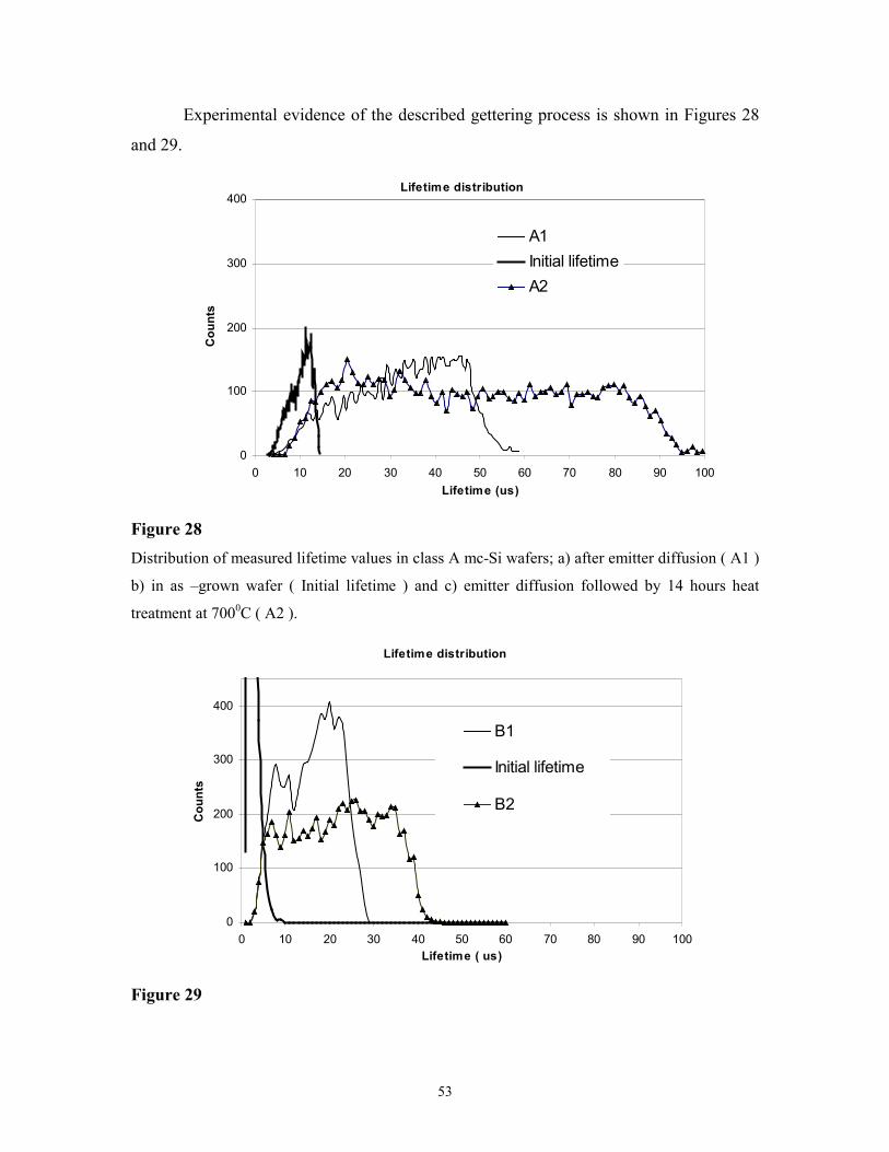
53
Experimental evidence of the described gettering process is shown in Figures 28
and 29.
Lifetime distribution
0
100
200
300
400
0 10 20 30 40 50 60 70 80 90 100Lifetime (us)
Cou
nts
A1Initial lifetimeA2
Figure 28 Distribution of measured lifetime values in class A mc-Si wafers; a) after emitter diffusion ( A1 )
b) in as –grown wafer ( Initial lifetime ) and c) emitter diffusion followed by 14 hours heat
treatment at 7000C ( A2 ).
Lifetime distribution
0
100
200
300
400
0 10 20 30 40 50 60 70 80 90 100Lifetime ( us)
Cou
nts
B1
Initial lifetime
B2
Figure 29
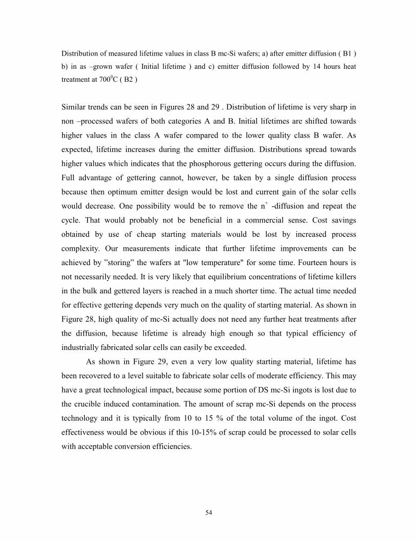
54
Distribution of measured lifetime values in class B mc-Si wafers; a) after emitter diffusion ( B1 )
b) in as –grown wafer ( Initial lifetime ) and c) emitter diffusion followed by 14 hours heat
treatment at 7000C ( B2 )
Similar trends can be seen in Figures 28 and 29 . Distribution of lifetime is very sharp in
non –processed wafers of both categories A and B. Initial lifetimes are shifted towards
higher values in the class A wafer compared to the lower quality class B wafer. As
expected, lifetime increases during the emitter diffusion. Distributions spread towards
higher values which indicates that the phosphorous gettering occurs during the diffusion.
Full advantage of gettering cannot, however, be taken by a single diffusion process
because then optimum emitter design would be lost and current gain of the solar cells
would decrease. One possibility would be to remove the n+ -diffusion and repeat the
cycle. That would probably not be beneficial in a commercial sense. Cost savings
obtained by use of cheap starting materials would be lost by increased process
complexity. Our measurements indicate that further lifetime improvements can be
achieved by ”storing” the wafers at "low temperature" for some time. Fourteen hours is
not necessarily needed. It is very likely that equilibrium concentrations of lifetime killers
in the bulk and gettered layers is reached in a much shorter time. The actual time needed
for effective gettering depends very much on the quality of starting material. As shown in
Figure 28, high quality of mc-Si actually does not need any further heat treatments after
the diffusion, because lifetime is already high enough so that typical efficiency of
industrially fabricated solar cells can easily be exceeded.
As shown in Figure 29, even a very low quality starting material, lifetime has
been recovered to a level suitable to fabricate solar cells of moderate efficiency. This may
have a great technological impact, because some portion of DS mc-Si ingots is lost due to
the crucible induced contamination. The amount of scrap mc-Si depends on the process
technology and it is typically from 10 to 15 % of the total volume of the ingot. Cost
effectiveness would be obvious if this 10-15% of scrap could be processed to solar cells
with acceptable conversion efficiencies.

55
8. Anti Reflection Coating
8.1 Properties of silicon nitride thin films grown by PECVD.
Plasma Enhanced Chemical Vapor Deposition ( PECVD ) has been recognized for many
years to be a key technology for deposition of passivating Si3N4 antireflection coatings.
The PECVD technique offers numerous advantages for processing of low cost solar cells.
First of all, PECVD is generally regarded as a low –cost processing technique, because
equipment throughput rates are high and large areas can be deposited during a process
cycle. PECVD deposition can be carried out within a temperature range from room
temperature up to more than 5000C. Dielectric thin films are usually grown at about
3000C, because at this temperature the density of pinholes is acceptably small and
formation of most common metal silicides does not take place. The low operating
temperature together with typically small thermal mass of the PECVD system offers the
above mentioned advantage of high throughput rate. Most importantly, low process
temperature enables to maintain a high minority carrier lifetime in low cost photovoltaic
grade silicon.
One general feature of plasma assisted deposition techniques compared to the
thermal processing of thin films, is the ability to adjust the film properties by changing
the process parameters. Relevant process parameters of PECVD are deposition pressure,
temperature, reactant gas mixture and power of the RF field exciting the plasma.
Reflection losses of the solar cell are mainly determined by the
optical properties of the antireflection coating. Thickness and refractive index of Si3N4
are chosen so that quarter wavelength destructive interference occurs at the wavelength
corresponding to the maximum of the solar cells internal quantum efficiency. Maximum
of the internal quantum efficiency depends on the sheet resistance of the emitter and the
diffusion length in the solar cell base region, but it is typically found between 500 –
600nm. Refractive index of the PECVD grown SiNx layer can be easily tuned between
1.9 and 2.1 giving film thickness of 60nm – 79nm.
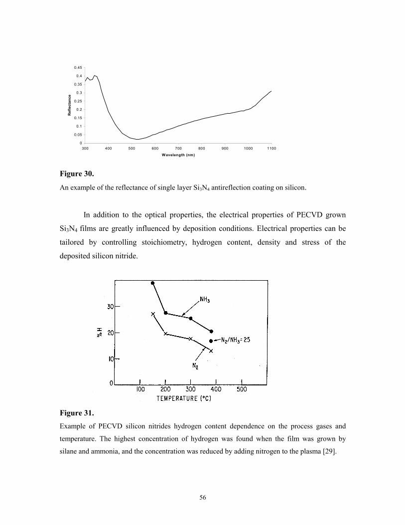
56
0
0.05
0.1
0.15
0.2
0.25
0.3
0.35
0.4
0.45
300 400 500 600 700 800 900 1000 1100
Wavelength (nm)
Ref
lect
ance
Figure 30.
An example of the reflectance of single layer Si3N4 antireflection coating on silicon.
In addition to the optical properties, the electrical properties of PECVD grown
Si3N4 films are greatly influenced by deposition conditions. Electrical properties can be
tailored by controlling stoichiometry, hydrogen content, density and stress of the
deposited silicon nitride.
Figure 31. Example of PECVD silicon nitrides hydrogen content dependence on the process gases and
temperature. The highest concentration of hydrogen was found when the film was grown by
silane and ammonia, and the concentration was reduced by adding nitrogen to the plasma [29].

57
High hydrogen content is wanted in photovoltaic applications, because hydrogen
can be diffused to the silicon –silicon nitride interface or to bulk by post deposition heat
treatment. Hydrogen is known to have beneficial effect in terms of reduced
recombination at the surface and bulk caused by passivation of dangling bonds and
defects [30].
8.2 Characterization of PECVD grown Si3N4
The Si3N4 antireflection coatings used in this work have been grown by parallel
plate type PECVD reactor operating at 13,56 MHz. This PECVD system is a single wafer
reactor equipped with sample holder designed especially for mc-Si substrates. Shower
head used for the process gas injection has been originally designed for round 2'' wafers
which seriously limits the ability of this system to deposit homogenous thin films on the
large surface area of square wafers.
Process gases used for ARC depositions were silane ( 1% in argon ), ammonia
and nitrogen. Silane is extremely reactive with oxygen. Because of safety issues a weak
gas solution has been chosen. Silicon nitride can be grown by using only silane and
ammonia, but it was very soon observed that the thickness variations in the Si3N4 films
were visible unless nitrogen was added to the plasma.
Another important factor determining the homogeneity of the Si3N4 films is the
substrate potential. During the deposition, the substrate is subjected to ion bombardment
which induces a negative surface potential. Ion bombardment affects film properties such
as stress, composition and structure [31]. The amount of ion bombardment can be

58
Effect of surface recombination velocity and fixed charge to IQE
0.0
10.0
20.0
30.0
40.0
50.0
60.0
70.0
80.0
90.0
100.0
380.0 480.0 580.0 680.0 780.0 880.0 980.0 1080.0 1180.0Wavelenght(nm)
IQE
neutral, no texturation,100 000cm/s
neutral, 100 000cm/s
0.1eV barrier, 100 000cm/s
0.1eV barrier, 10 0cm/s
Figure 32. Effect of surface recombination velocity and fixed dielectric charge to internal quantum
efficiency of solar cell. The simulation has been carried out with PC1D.
adjusted to some extent by controlling the proportion of inert gas species in the plasma. If
nitrogen and argon are added to the plasma, ion bombardment is significant. It is
therefore important that the whole rear side of the substrate is contacted with sample
holder in order to ensure homogeneous potential distribution across the wafer. Prior to the
Si3N4 deposition the vacuum chamber was cleaned by SF6 plasma which removes
insulating residuals from the chamber walls and the sample holder. Plasma cleaning was
followed by test deposition using a dummy wafer. During the test deposition the chamber
wall and the sample holder became coated everywhere except under the substrate. The
growth rate and the refractive index of the Si3N4 films were checked by ellipsometer. All
depositions have been carried out at 3000C. RF power has been varied from 50W to
150W, giving a growth rate of about 8 – 12 nm/min , depending on the deposition
pressure.

59
In addition to antireflection properties of Si3N4 films, passivation is an important
feature which correlates strongly to the conversion efficiency. In the case of photovoltaic
devices, passivation means elimination of surface recombination velocity. Silicon –
silicon nitride interface of the solar cells can be passivated by two ways, reducing the
density of the interface states or by introducing an electric field which is repulsing
minority carriers from the surface. Surface recombination velocity, sample thickness and
bulk lifetime determine the effective lifetime which can be measured for example with
the µPCD method. These parameters are related to each other by Eq. (24) [7]. The
parameter β contains information about the surface recombination and if solved from Eq.
(24) is given by
βτ τ
= −
1 1 1D eff bulk
, (43)
where D is the diffusion coefficient for the minority carriers. β is a transcendental
function of wafer thickness, and the front and back surface recombination velocities
( )tan( ) ( )β ββ
T s sD s s
= +−
1 22 2
1 2
(44)
[ ]ss T
D T s12
22=
+−β
β ββ β
tan( )tan( ) . (45)
If the surface recombination velocity at the rear side of the wafer approaches zero, the
front surface recombination velocity can be approximated by the following expression:
s
s D TDeff bulk eff bulk
2
1
0
1 1 1 1 1
→
= −
−
τ τ τ τ
tan . (46)
Equation 46. implies that if the wafer thickness and the difference between effective and
bulk lifetimes are known, the surface recombination velocity can be easily calculated.

60
The following experiment was carried out in order to investigate the passivation
efficiency of PECVD grown silicon nitride. A 40nm thick Si3N4 layer was grown on a
polished Cz –wafer having a resistivity of 4-6 Ωcm. The deposition pressure was
600mTorr and the RF power was 200W at 13,56 MHz. The process gas flows were
chosen so that the refractive index of the silicon nitride was 2,0 . The effective lifetime
was mapped by a lifetime scanner so that the back side of the wafer was passivated by
iodine ethanol solution. After the measurement, the Si3N4 film was removed by HF.
Finally, the bulk lifetime was measured by putting the bare wafer to plastic envelope
filled with an iodine ethanol passivation solution. The Lifetime charts are presented in
Figure 32.
Figure 33.
µPCD lifetime charts. Back side of the wafer has been passivated by iodine ethanol solution and
front side by 40nm thick Si3N4 ( left ). Lifetime chart after removal of Si3N4 , the whole wafer
passivated by iodine ethanol ( right )
It can be clearly seen that both lifetime maps as well as numerical distributions of the
measurement points are very similar. For example, belt carrier contamination is identified
by two red stripes in the lower half of the maps. Since the only difference in these two
measurements is the passivation of the front surface, it can be concluded that PECVD
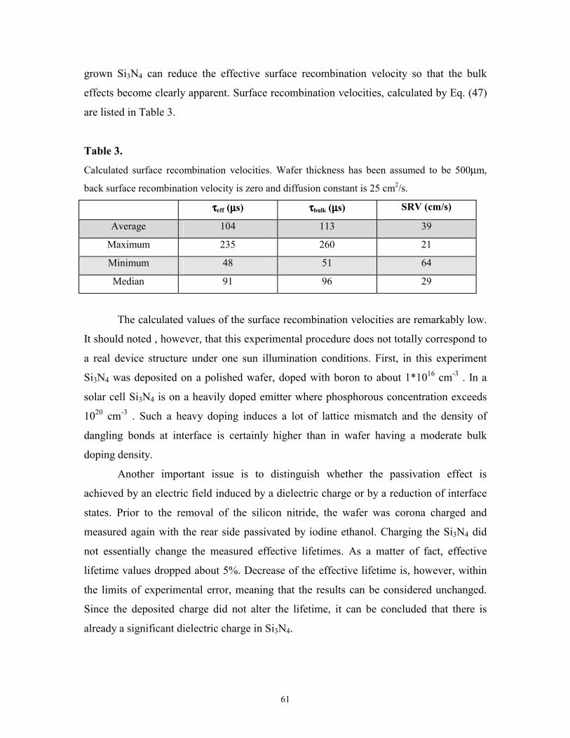
61
grown Si3N4 can reduce the effective surface recombination velocity so that the bulk
effects become clearly apparent. Surface recombination velocities, calculated by Eq. (47)
are listed in Table 3.
Table 3.
Calculated surface recombination velocities. Wafer thickness has been assumed to be 500µm,
back surface recombination velocity is zero and diffusion constant is 25 cm2/s.
ττττeff (µµµµs) ττττbulk (µµµµs) SRV (cm/s)
Average 104 113 39
Maximum 235 260 21
Minimum 48 51 64
Median 91 96 29
The calculated values of the surface recombination velocities are remarkably low.
It should noted , however, that this experimental procedure does not totally correspond to
a real device structure under one sun illumination conditions. First, in this experiment
Si3N4 was deposited on a polished wafer, doped with boron to about 1*1016 cm-3 . In a
solar cell Si3N4 is on a heavily doped emitter where phosphorous concentration exceeds
1020 cm-3 . Such a heavy doping induces a lot of lattice mismatch and the density of
dangling bonds at interface is certainly higher than in wafer having a moderate bulk
doping density.
Another important issue is to distinguish whether the passivation effect is
achieved by an electric field induced by a dielectric charge or by a reduction of interface
states. Prior to the removal of the silicon nitride, the wafer was corona charged and
measured again with the rear side passivated by iodine ethanol. Charging the Si3N4 did
not essentially change the measured effective lifetimes. As a matter of fact, effective
lifetime values dropped about 5%. Decrease of the effective lifetime is, however, within
the limits of experimental error, meaning that the results can be considered unchanged.
Since the deposited charge did not alter the lifetime, it can be concluded that there is
already a significant dielectric charge in Si3N4.

62
The importance of fixed dielectric charge is illustrated in Figure 31 which present
simulations of efficiency versus field effect passivation and surface recombination
velocity.
63
9. Contacts of solar cells
The front contact of the solar cell is a grid of metal fingers that cover typically 5 -
10 % of the area of the cell. Solar cells are designed to create electrical power. The
current density is therefore high in front contact fingers. For example, a 100cm2 solar cell
generates about 3A under AM1.5G illumination, the number of contact fingers is 100 and
there are two busbars collecting the current to the external circuit. The width of the finger
is 20µm and height is 10µm giving a cross sectional area of 2*10-6 cm2 . Current density
near the point where the finger and busbar are connected is then 3750 A/cm2.
In scope to get good device performance, the power losses due to the contacts
must be minimized. An additional requirement for the contacts is set by the economical
constraints of mass production feasibility. The coverage of the front contact determines
the shadowing losses that can be observed directly in the solar cells’ output
characteristics. Because the total area of the front contact is limited in order to keep the
shadowing losses on a reasonable level, the length and width of the contact fingers are
constant. Therefore there are two ways to reduce the resistance of the grid finger without
increasing the shadowing losses, to increase the thickness and to decrease the resistivity
of the contacting material.
The most common contact grid design for large area solar cells is the so called H
–figure. It consist of two wide busbars and fingers perpendicular to busbars. When the
solar cells are assembled to a module, the busbars are soldered with thick metal stripes
which are then connected to solder joints on the back contact of the next solar cell. Solar
cells made by “low cost” process described in this work are processed on 10cm X 10cm
square multicrystalline silicon substrates and all devices have the same contact grid
structure. The distance between the busbars is 4,8 cm and the width of the busbars is
1,5mm, giving a total shadowed area of 3cm2 . The number of fingers is 110 . The width
of the metal fingers is 10µm on the photomask. The fingers tend to spread modestly
during the lithography and etching, and significantly during the electroplating. Finger
width after electroplating of copper is determined by SEM and it is about 20µm when
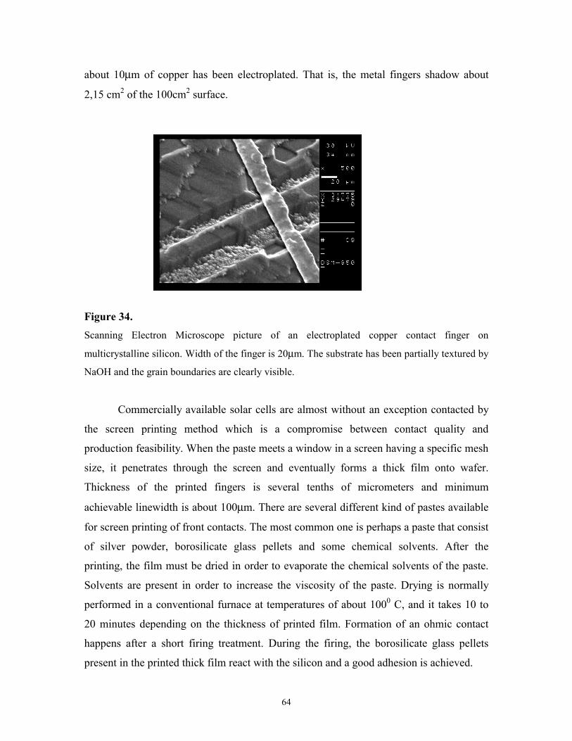
64
about 10µm of copper has been electroplated. That is, the metal fingers shadow about
2,15 cm2 of the 100cm2 surface.
Figure 34. Scanning Electron Microscope picture of an electroplated copper contact finger on
multicrystalline silicon. Width of the finger is 20µm. The substrate has been partially textured by
NaOH and the grain boundaries are clearly visible.
Commercially available solar cells are almost without an exception contacted by
the screen printing method which is a compromise between contact quality and
production feasibility. When the paste meets a window in a screen having a specific mesh
size, it penetrates through the screen and eventually forms a thick film onto wafer.
Thickness of the printed fingers is several tenths of micrometers and minimum
achievable linewidth is about 100µm. There are several different kind of pastes available
for screen printing of front contacts. The most common one is perhaps a paste that consist
of silver powder, borosilicate glass pellets and some chemical solvents. After the
printing, the film must be dried in order to evaporate the chemical solvents of the paste.
Solvents are present in order to increase the viscosity of the paste. Drying is normally
performed in a conventional furnace at temperatures of about 1000 C, and it takes 10 to
20 minutes depending on the thickness of printed film. Formation of an ohmic contact
happens after a short firing treatment. During the firing, the borosilicate glass pellets
present in the printed thick film react with the silicon and a good adhesion is achieved.

65
The disadvantages of the screen printing method are the questionable quality of
contacts and the process complexity. The conductivity of the screen printed grid fingers is
significantly lower than in those fabricated by depositing some bulk metal. The process
complexity arises from the fact that in addition to printing, the contacts need some drying
and firing. Both process steps are time consuming and especially the firing of the contacts
is known to be “ state of art “. It should also be noted that after each printing, the screen
printer needs careful cleaning.
The metallization scheme described in this chapter is in contrast to screen printing
realizable only by using optical lithography and by vacuum chamber based deposition
techniques. Basic idea of the metallization process described in this thesis is first to
deposit a thin metal layer that adheres well to silicon, is not, or is in a very small scale
alloying with the silicon and provides a low contact resistance. The second layer will be a
metal having a high conductivity. Typical widely used adhesion layer metals are for
example titanium, titanium tungsten, chromium and molybdenum. High conductivity
metals are for example copper, silver and gold.
The use of multilayer contact structures sets certain requirements to the metallization
process itself. First, the adhesion metals are unfortunately oxidized very rapidly. It means
that the second metal must be deposited in the same vacuum chamber. Otherwise the
interface between the first and the second films will be of a very low quality and results
in a poor ohmic contact. Secondly, typical adhesion metals have quite a low conductivity
and the deposited layers should be relatively thin. Thin adhesive metal films are usually
called flash -layers and their thicknesses are normally between 50nm and 150nm.
Chromium and copper forms a fascinating material system that has been widely
used for many IC chip packaging applications. This material system has not been widely
used for microelectronics fabrication itself, mostly because copper is known to be
extremely harmful contaminant and a effective charge carrier lifetime -killer in silicon.
However, if the processing after the copper deposition is done at low temperatures ( <
2000C ) and the operating temperatures of the device are low, the copper induced
contamination problems do not exist [30]. This allows to combine effectively the
excellent adhesion properties of chromium and the high conductivity of copper. In
addition, both materials are cheap and they can be utilized in solar cells in a cost -
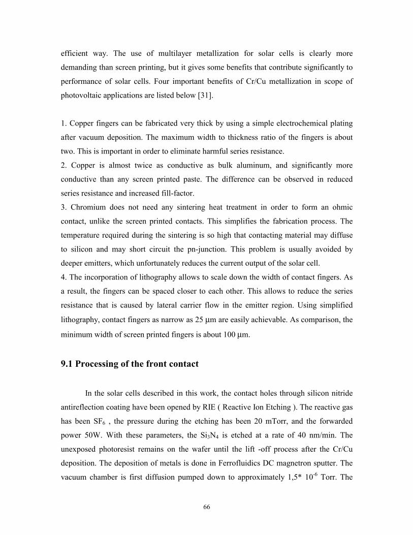
66
efficient way. The use of multilayer metallization for solar cells is clearly more
demanding than screen printing, but it gives some benefits that contribute significantly to
performance of solar cells. Four important benefits of Cr/Cu metallization in scope of
photovoltaic applications are listed below [31].
1. Copper fingers can be fabricated very thick by using a simple electrochemical plating
after vacuum deposition. The maximum width to thickness ratio of the fingers is about
two. This is important in order to eliminate harmful series resistance.
2. Copper is almost twice as conductive as bulk aluminum, and significantly more
conductive than any screen printed paste. The difference can be observed in reduced
series resistance and increased fill-factor.
3. Chromium does not need any sintering heat treatment in order to form an ohmic
contact, unlike the screen printed contacts. This simplifies the fabrication process. The
temperature required during the sintering is so high that contacting material may diffuse
to silicon and may short circuit the pn-junction. This problem is usually avoided by
deeper emitters, which unfortunately reduces the current output of the solar cell.
4. The incorporation of lithography allows to scale down the width of contact fingers. As
a result, the fingers can be spaced closer to each other. This allows to reduce the series
resistance that is caused by lateral carrier flow in the emitter region. Using simplified
lithography, contact fingers as narrow as 25 µm are easily achievable. As comparison, the
minimum width of screen printed fingers is about 100 µm.
9.1 Processing of the front contact
In the solar cells described in this work, the contact holes through silicon nitride
antireflection coating have been opened by RIE ( Reactive Ion Etching ). The reactive gas
has been SF6 , the pressure during the etching has been 20 mTorr, and the forwarded
power 50W. With these parameters, the Si3N4 is etched at a rate of 40 nm/min. The
unexposed photoresist remains on the wafer until the lift -off process after the Cr/Cu
deposition. The deposition of metals is done in Ferrofluidics DC magnetron sputter. The
vacuum chamber is first diffusion pumped down to approximately 1,5* 10-6 Torr. The

67
deposition pressure is set to about 1,3*10-3 Torr by balancing the argon flow and the out
pumping. This value of the sputtering pressure is as low as necessary to turn on the argon
plasma in the vacuum chamber. Low sputtering pressure has been observed to induce a
large tensile stress into the chromium film. The presence of the tensile stress was found to
be essentially important for the following lift off.
The lift off is carried out by placing the wafers in acetone in an ultra sonic bath.
Sputtering parameters and choice of the barrier materials determine the time needed for
the complete lift off of the metals elsewhere than in the opened contact areas. For
example, if the metallization was done by sputtering of chromium as described above, the
lift off time is about 1-2 minutes. If the metallization was done by sputtering of ,e.g.,
tungsten –copper or titaniumtungsten ( 10/90 ) –copper multilayer structures, more than
30 minutes in the acetone ultra sonic bath was required. Profilometer measurements of
the wafer bow indicated that there is 5-10 times larger tensile stress in Cr/Cu metallized
wafers than in W/Cu or TiW/Cu samples.
The thickness of the sputtered metal contact grid is less than 300nm which is at
least an order of magnitude less than the required thickness for suppression of the series
resistance of the solar cell to an acceptable level. The contact grid is reinforced by
electroplating more copper on the sputtered grid. Electroplating is metal deposition by
electrolysis from an aqueous metal salt solution [30]. It is generally carried out at near
room temperature. The electroplating setup used in this work is self constructed and it
consist of two electrodes immersed in a copper plating, external power supply, magnetic
stirrer and PC. The electrodes are made of copper in order to decrease the rate of
impoverishment of the copper bath. The counter electrode has a form of six-pronged fork,
approximately the same size as the solar cell. Electroplating takes place only on the
electrically conductive areas of the wafer when the positively charged metal ions flow to
the negatively biased Cr/Cu grid where they acquire electrons. Copper electroplating
recipe is based on the following commercially available ingredients and deionized water;
Copper Gleam Concentrate ( Coppersulphide )1020 ml Sulphuric Acid 98% 360 ml Copper Gleam 125T Additive 2,5 ml DIW 1400 ml

68
T=370C
The growth rate as well as the homogeneity of the plated film is sensitive to the applied
current density. The manufacturer of Copper Gleam concentrate guarantees a growth rate
of 1,25µm/min for a current density of 100mA/cm2 . It was, however, observed that when
the driving current of the plating was kept constant, the result was inhomogeneous
thickness of copper fingers. The current-voltage source was therefore programmed so that
the current increases linearly up to 0,5A during the first five minutes. The next five
minutes the current was kept constant at 0,5A which resulted in the final thickness of the
copper fingers to be approximately 10µm.
9.2 Processing of the back contact and the Back Surface Field ( BSF )
The back contacts of solar cells are made of aluminum. Commercially fabricated solar
cells are back contacted by screen printing of aluminum. Typically the aluminum
metallization covers the whole back surface and there are some silver solder joints on the
aluminum, also made by screen printing. The solder joints are needed for module
assembly. In view of the series resistance, the whole back surface would not need to be
completely contacted. As it is in the case of the front contacts, 5-10% of the total area is
required to provide series resistance low enough for solar cell applications. Therefore in
some commercial solar cell configurations, the back side metallization is printed through
a mesh grid because of material consumption savings. In this work, however, the solar
cells are back contacted by sputtered bulk aluminum. During the electroplating of the
front contact, there used to be some parasitic copper deposition also on the back side of
the wafers which indeed enabled to solder the module contact wires to the cells made by
this method.
The efficiency of the solar cell can be improved by processing techniques related
to the back contact formation. The lifetime can be improved by aluminum gettering
which takes place during the heat treatment necessary for ohmic contact formation. The
lifetime improvement is, however, limited because the gettering efficiency obviously
depends on the duration and the temperature of the annealing. The diffusion profile

69
should not be essentially altered during the aluminum annealing, which sets the upper
limit of the usable temperature to about 8000C. Another possibility to increase the
efficiency by aluminum annealing is to create a doping gradient near the back surface
which exhibits a high surface recombination velocity. This doping gradient which drifts
the minority carriers towards the pn-junction is called the Back Surface Field ( BSF ) and
it can be realized by aluminum because it is a p-type dopant in silicon. The other
possibilities to establish a low back surface recombination velocity to a silicon solar cell
is to process p+ -doping gradient by boron diffusion or passivate the back surface by
thermally grown SiO2 . The principle of BSF is illustrated in Figure 34 in terms of energy
band diagrams.
Figure 35. The energy band diagram obtained by PC1D simulation of a solar cell with BSF. For clarity, the
solar cell is hypothetically only 5µm thick.
The functionality of the BSF is nicely demonstrated in Figure 35, which shows a LBIC (
Laser Beam Induced Current ) map of a BSF solar cell. The LBIC map is basically a
position resolved measurement of the short circuit current. In this particular solar cell the
diffusion length exceeds the wafer thickness, the front surface is passivated by thermal
Energy Band diagram of BSF solar cell
-1.2
-1
-0.8
-0.6
-0.4
-0.2
0
0.2
0.4
0.6
0.00E+00 1.00E-06 2.00E-06 3.00E-06 4.00E-06 5.00E-06
Distance (m)
eV
Conduction Band Edge
Valence Band Edge
Electron Quasi-Fermi Energy
Hole Quasi-Fermi Energy

70
SiO2 and the BSF is made by screen printed aluminum. Screen printed silver solder joints
are clearly distinguished as high back surface recombination velocity areas.
Figure 36. LBIC map of a 14,9% efficient mc-Si solar cell. This solar cell is processed by ASE Ltd. and the
mc-Si substrate is from the same manufacturer as the wafers used in this work. High back surface
recombination velocity, i.e. silver metallized, areas are clearly visible.
Thickness of the aluminum used in this work has been about 2µm. The formation
of a Back Surface Field ( BSF ) by aluminum alloying process is in practice a very
difficult task. Therefore the solar cells described in this work have been sintered with
thermal cycles that result in a ohmic contact, but no BSF has been formed to the back
side of the solar cells. The front contact metallization contact holes are patterned to
PECVD grown silicon nitride antireflection coating by reactive ion etching in SF6. The
unexposed photoresist remains on the wafer until the lift -off process after the self –
aligned Cr/Cu deposition. The deposition of metals is done in a DC magnetron sputter.
The front contacts are finished by electrochemical deposition of copper.
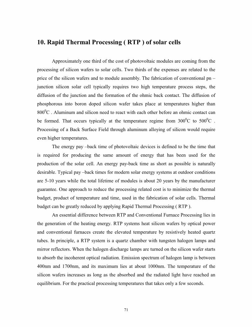
71
10. Rapid Thermal Processing ( RTP ) of solar cells
Approximately one third of the cost of photovoltaic modules are coming from the
processing of silicon wafers to solar cells. Two thirds of the expenses are related to the
price of the silicon wafers and to module assembly. The fabrication of conventional pn –
junction silicon solar cell typically requires two high temperature process steps, the
diffusion of the junction and the formation of the ohmic back contact. The diffusion of
phosphorous into boron doped silicon wafer takes place at temperatures higher than
8000C . Aluminum and silicon need to react with each other before an ohmic contact can
be formed. That occurs typically at the temperature regime from 3000C to 5000C .
Processing of a Back Surface Field through aluminum alloying of silicon would require
even higher temperatures.
The energy pay –back time of photovoltaic devices is defined to be the time that
is required for producing the same amount of energy that has been used for the
production of the solar cell. An energy pay-back time as short as possible is naturally
desirable. Typical pay –back times for modern solar energy systems at outdoor conditions
are 5-10 years while the total lifetime of modules is about 20 years by the manufacturer
guarantee. One approach to reduce the processing related cost is to minimize the thermal
budget, product of temperature and time, used in the fabrication of solar cells. Thermal
budget can be greatly reduced by applying Rapid Thermal Processing ( RTP ).
An essential difference between RTP and Conventional Furnace Processing lies in
the generation of the heating energy. RTP systems heat silicon wafers by optical power
and conventional furnaces create the elevated temperature by resistively heated quartz
tubes. In principle, a RTP system is a quartz chamber with tungsten halogen lamps and
mirror reflectors. When the halogen discharge lamps are turned on the silicon wafer starts
to absorb the incoherent optical radiation. Emission spectrum of halogen lamp is between
400nm and 1700nm, and its maximum lies at about 1000nm. The temperature of the
silicon wafers increases as long as the absorbed and the radiated light have reached an
equilibrium. For the practical processing temperatures that takes only a few seconds.
72
Figure 37. Principle of RTP system.
In view of photovoltaic applications, RTP technology offers several benefits.
According to its name, RTP is a rapid process thus potentially allowing very high
throughput rate of the process wafers. In contrast to conventional furnaces, process times
are usually counted in seconds or tens of seconds, when typical quartz tube furnace
diffusion may take up to several hours. High throughput rate sounds very fascinating if a
large scale production of solar cells is considered. Since the RTP is carried out in
atmospheric pressure conditions, a high degree of automation could be implemented.
Industrial manufacturing of solar cells is usually carried out by belt carrier furnaces
which could be easily equipped with tungsten discharge lamps.
Another advantage of RTP is its cold –wall reactor nature. In the first
approximation, in RTP only the substrate is heated, not the chamber wall or sample
holders etc. If cold –wall reactors are used for solar cell processing it is obvious that the
energy pay –back time will be reduced and no energy is lost for heating the large thermal
mass of the quartz tube furnace. Also process equipment induced contamination is a less
severe problem in a cold –wall reactor than in a hot –wall furnace tube.
Because of the benefits mentioned above, the RTP technology has been believed
to have potential for mass production of solar cells [32]. Rapid processing of silicon
73
wafers has therefore gained a lot of academic interest among photovoltaic researchers.
Despite of the fact that RTP is widely used in microelectronics for recrystallization of the
ion implanted layers and in epitaxial wafer production, it has not been used this far for
commercial manufacturing of silicon solar cells. RTP technology unfortunately has some
drawbacks that become crucial when large area and low cost silicon wafers come into
question. Fast thermal processing namely means not only high throughputs but also large
temperature gradients [33]. Temperature gradients in turn lead unavoidably to stress
within the volume of the silicon wafer. The thermoelastic stress generated by a
temperature gradient is expressed in terms of polar coordinates by the following
equations
−
−=
rr
wrr rdrrT
rrdrrT
rE w
02
02
*
)(1)(11 νασ ν , (48)
−+
−=
rr
w
rTrdrrTr
rdrrTr
E w
02
02
*
)()(1)(11 νασ ν
θθ , (49)
where 2rw is the wafer diameter, T(r) is the temperature gradient, E* is Young’s modulus,
ν is the Poisson’s ratio and αν is the coefficient of thermal expansion. If thermoelastic
stresses exceed a certain value, thermoplastic effects take place. That value is called yield
strength and it is given by
kTmE
mc
a
edcdT **1
* )(),( =σ , (50)
where Ea is the activation energy of line defect movement, d is the strain rate and m* and
c* are material constants. For silicon m* is 2,9 –3,4 in the temperature range between
8000C and 13000C. It should be noted that m* and c* are affected by impurities in the
silicon crystal.
The temperature gradients appear across the wafer because radiative heat loss is
larger at the edge regions than in the center of the substrate. The edge of the wafer is

74
cooler than the center. More dominating origin of the thermal gradient is, however, the
radially non –ideally uniform optical energy source of the halogen lamps. In a real RTP
system it is very difficult to control the homogeneity of the optical power transmitted by
the discharge lamps. The temperature of the silicon wafer is measured by a pyrometer or
by a thermocouple which is in physical contact with the back side of the substrate.
Temperature control is carried out by a feedbacked loop between the temperature sensor
and the power source of the discharge lamps. Since the number of temperature
measurement points and speed of the control electronics are limited, illumination of the
wafer is very seldom homogenous. That is especially true when large areas of silicon
need to be processed in short times, for instance in a couple of seconds. When the stresses
created by the thermal gradient exceed the yield strength, they will be relaxed by
generation of dislocations. These dislocations are called slip defects. Slip defects are line
defects whose startpoints are at the wafer edges and they are generated along certain well
–defined crystallographic directions. In the case of silicon, slips exist at (111) planes and
their direction is <110> . There are 12 different slip systems possible but because of
silicon’s diamond cubic lattice symmetry, only five slip directions are independent of
each other.
Figure 38 Five slip defect directions in (100) orientated silicon wafer. This kind of defects are often visible
by naked eye.
75
The temperature gradient induced defects are naturally harmful for solar cells operational
performance. Line defects at wafer edges short circuit the pn –junction and thus degrade
the conversion efficiency. Defect generation is the main drawback of the RTP technology
preventing its large scale utilization for solar cell processing.
10.1 Experimental
In this project, about seventy 100 cm2 mc –Si wafers have been rapid thermal
processed to solar cells in year 2000. The RTP system used for these experiments is
Heatpulse 2101 and it is located in the cleanroom of the Microelectronics Centre of HUT.
The useful temperature range of this system is from 4000C to 11500C, with a heating rate
of 100C – 3000C per second.
If high temperature process steps, emitter diffusion and back contact heat
treatment, are excluded, the processing of RTP solar cells is similar to conventional solar
cells. The wafers are first subjected to wet chemical treatments, alkaline damage etch
followed by RCA cleaning. Phosphorous diffusion source has been spin –on deposited.
Four milliliters of Filmtronics P509 Spin –On Dopant ( SOD ) was dispensed on the
wafers and spinned with 1500 rpm’s for 35 seconds. Prior to diffusion, the SOD film was
dried in an air convection furnace at 1200C for 30 minutes.
A set of different RTP diffusion profiles was realized in order to find out the near
optimum process parameters [34]. The temperature in RTP chamber was first ramped up
to about 7000C followed by a stabilization of 60 s. The best results were obtained by
ramping up at 1000C/min to the peak temperature of 8700C for 60 seconds yielding a
sheet resistance of about 100Ω/sqr. The diffusion is followed by fast ramping down at the
rate of about 1000C/min to 7000C stabilization temperature for 60 s.
The diffusion is followed by SOD removal, cleaning, silicon nitride PECVD
deposition and aluminum sputtering performed in the same manner as the corresponding
process steps in the “low cost” process described in previous Chapters. The aluminum
76
heat treatment was made by RTP at 4500C for five minutes. The attempts to process an
aluminum BSF at temperatures higher than 5770C were not successful. An excessive
reflow of aluminum took place during the rapid processing and the back contact of the
solar cells was partially degraded. The solar cells were finished by processing the front
contact as described in Chapter 8.
77
11. Processing of single crystalline silicon solar cells
The objective of process development of single crystalline silicon ( c –Si ) solar cells is to
evaluate the limits for the conversion efficiency. The process sequence of c –Si solar cells
is essentially more complex than the earlier described fabrication of mc –Si devices.
Although the relevance for the commercial production is possibly minimal, the
processing of high efficiency solar cells has provided lot of valuable information about
the efficiency loss mechanism in mc –Si cells.
The most significant contributor to the higher efficiency of cells made of single
crystalline material is the higher minority carrier lifetime. That is due to the well –
established Czochralski ( Cz ) ingot pulling technology which is only shortly described in
this work. The raw material of the cz –Si wafers, semiconductor grade polysilicon, is
basically the same as solar cell substrates. Semiconductor grade polysilicon is the third
phase of a complex manufacturing sequence starting from silica, the most abundant
compound on the earth, and leading to nearly perfect single crystals of extreme purity.
Silica is silicon dioxide containing lot of impurities.
11.1 Substrate technology
Oxygen is reduced from the silica in large furnaces at temperatures higher than
20000C . The resulting compound is called metallurgical silicon ( Mg-Si ) and its purity is
typically 99% . One percent impurity concentration consists mainly of iron, aluminum,
carbon and silicon carbide. This level of purity is far too low for any semiconductor
device applications. The further purification which is necessary for ” parts per billion ”
class of cleanliness is achieved with the help of hydrogen chloride ( HCl ) . HCl is passed
through pulverized Mg –Si in a special reactor. The resulting species are hydrogen, HCl,
unreacted silicon and at the proper process conditions, different cholorosilane
compounds. These compounds are trichlorosilane ( TCS ) and silicon tetrachloride ( STC
) . Purification of cheap Mg-Si by cheap HCl has now led to very pure chemicals that can
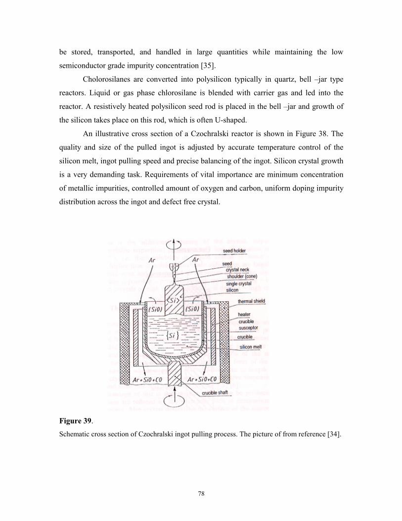
78
be stored, transported, and handled in large quantities while maintaining the low
semiconductor grade impurity concentration [35].
Cholorosilanes are converted into polysilicon typically in quartz, bell –jar type
reactors. Liquid or gas phase chlorosilane is blended with carrier gas and led into the
reactor. A resistively heated polysilicon seed rod is placed in the bell –jar and growth of
the silicon takes place on this rod, which is often U-shaped.
An illustrative cross section of a Czochralski reactor is shown in Figure 38. The
quality and size of the pulled ingot is adjusted by accurate temperature control of the
silicon melt, ingot pulling speed and precise balancing of the ingot. Silicon crystal growth
is a very demanding task. Requirements of vital importance are minimum concentration
of metallic impurities, controlled amount of oxygen and carbon, uniform doping impurity
distribution across the ingot and defect free crystal.
Figure 39.
Schematic cross section of Czochralski ingot pulling process. The picture of from reference [34].
79
Polysilicon fragments are placed into quartz crucible and melted by a heater. The melting
point of the silicon is 14150C. The whole system is sealed in an inert gas and the crucible
is placed in a graphite susceptor which is in a slow rotational movement. First a seed
crystal is immersed into the liquid silicon. Then the seed crystal is pulled slowly upwards
without breaking the solid –liquid interface. The slow cooling during pulling makes the
solidifying molten silicon to follow the crystallographic structure of the seed single
crystal. The pulling of a typically about two meters long ingot takes more than two days.
The polysilicon starting material has been purified by a sophisticated process but
it is not free of impurities. Single crystalline silicon grown by Czochralski method is
unquestionably the dominating substrate material for the modern microelectronics. One
reason for that is the effect of the material purification during the crystal growth. In
silicon technology, metals are typically the impurities of largest quantities and major
concerns. During the Czochralski ingot pulling there exist two phases, solid and liquid.
The interface region between solid and liquid silicon plays an important role in
determining the resulting material quality. Concentration of many metals around a given
temperature is usually different in a frozen solid than in molten silicon. Crystal growth
related impurity kinetics is modeled with an equilibrium distribution coefficient, often
referred to as the segregation coefficient, which is given by
)ln()ln( 0 γσ +∆−+∆−∆=R
SRT
HHKfsf
, (51)
where ∆Hf is the heat of the fusion between the melting point of the impurity and the
melting point of the silicon, ∆Hs is the differential heat of the solution of the impurity in
the silicon, ∆Sf is the entropy of the fusion of the impurity at its melting point, σ is the
change in vibrational entropy which results from the transfer of the impurity from its
lattice site to new one in silicon, R is the molar gas constant, T is the temperature and γ is
an activity coefficient. At the melting point of the silicon, the impurities will accumulate
at the solid-liquid interface region if the segregation coefficient of the impurity is less
than one. An opposite kinetics will take place if the impurity owns a segregation
coefficient greater than one. A list of experimentally determined segregation coefficients

80
of the most common impurities involved with silicon technology are presented in Table
4.
Table 4.
Segregation coefficients of some materials that have importance in silicon technology.
Impurity K0
Iron 8*10-6
Copper 4*10-4
Gold 2,5*10-5
Aluminum 0,002
Boron 0,8
Phosphorous 0,35
Arsenic 0.3
As it can be seen in Table 4, impurities that form the most active recombination centers
in silicon, i.e. metals, have fairly low values of segregation coefficient. Accumulation of
iron, copper, gold and many other metals into the solid-liquid boundary region is a
fortunate coincidence because that leads to a purification of the ingot to pulled.
Elsewhere, during the crystal growth process the molten silicon in the quartz crucible will
be enriched by these impurities. On the other hand, it is also inconsiderable that the
common doping impurities have segregation coefficients close to one unity. That makes
it possible to dope silicon crystals homogeneously. Commonly seen larger resistivity
variations in n –type ingots, doped by phosphorous or arsenic, compared to the boron
doped p –type ones are a consequence of different segregation coefficients.
Impurity segregation during the crystal processing explains the higher minority
carrier lifetime in Czochralski grown silicon compared with the multicrystalline wafers
made by Direct Solidification method. Minimal density of defects and high lifetime are
fundamental necessities when a conversion efficiency as high as possible is pursued.
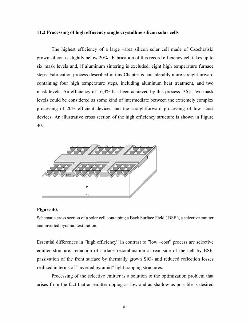
81
11.2 Processing of high efficiency single crystalline silicon solar cells
The highest efficiency of a large –area silicon solar cell made of Czochralski
grown silicon is slightly below 20% . Fabrication of this record efficiency cell takes up to
six mask levels and, if aluminum sintering is excluded, eight high temperature furnace
steps. Fabrication process described in this Chapter is considerably more straightforward
containing four high temperature steps, including aluminum heat treatment, and two
mask levels. An efficiency of 16,4% has been achieved by this process [36]. Two mask
levels could be considered as some kind of intermediate between the extremely complex
processing of 20% efficient devices and the straightforward processing of low –cost
devices. An illustrative cross section of the high efficiency structure is shown in Figure
40.
Figure 40. Schematic cross section of a solar cell containing a Back Surface Field ( BSF ), a selective emitter
and inverted pyramid texturation.
Essential differences in ”high efficiency” in contrast to ”low –cost” process are selective
emitter structure, reduction of surface recombination at rear side of the cell by BSF,
passivation of the front surface by thermally grown SiO2 and reduced reflection losses
realized in terms of ”inverted pyramid” light trapping structures.
Processing of the selective emitter is a solution to the optimization problem that
arises from the fact that an emitter doping as low and as shallow as possible is desired

82
because of the high current gain. This is contradictory with the demand for very high
doping levels required for good ohmic contacts. In a selective emitter of a solar cell there
is heavy and deep diffusion under the busbars and contact fingers, but moderate
concentration of phosphorous in the areas not covered by metal. An additional benefit is
obtained when the pn-junction distance is larger from the high recombination rate contact
area that takes up approximately 5% of the front surface.
The processing of single side polished wafers starts with potassiumhydroxide (
KOH ) wet etching which reduces the wafer thickness from the standard 500µm closer to
the optimal thickness of a solar cell. Optimal thickness of the solar cell is not an
unambiguous parameter but rather a variable that depends on the diffusion length of
electrons, the surface recombination rate at both surfaces and the absorption of light in
silicon. Best open circuit voltages can be theoretically obtained from cells which are
approximately 100µm thick. Mechanical rigidity of the silicon of this thickness is so poor
that the wafers are usually left 200 -250µm thick in high efficiency device experiments.
The thinning of the wafers in boiling KOH is followed by RCA cleaning. A short
dip in aqueous HCl is carried prior to RCA in order to prevent alkaline contamination of
the quartz cleaning solution containers. Filmtronics P509 spin on dopant is used as a
phosphorous source for the first diffusion. A relatively high diffusion temperature, 9000C,
is used to provide a low sheet resistance value of approximately 15 Ω / square. SOD
residuals are removed in BHF after the diffusion.
Selective anisotropic wet etching of silicon requires a mask material which is
resistant against the etchant itself. In the case of KOH etching, the erosion of the masking
material is often a subject of concern. Thermally grown silicondioxide and LPCVD (
Low Pressure Chemical Vapor Deposition ) deposited silicon nitride are commonly used
etch mask materials in silicon micromechanics. Both deposition methods are high
temperature processes and therefore potential sources of lifetime degradation. PECVD
deposited silicon nitride has been found to be a suitable mask for etching of inverted
pyramids. It has turned out that PECVD Si3N4 grown by our standard ARC recipe at
3000C is resistant enough for that application.
After the growth of the etch mask film, the wafers are subjected to the first
photolithography. The photomask has the same shape as the front contact grid. Contact
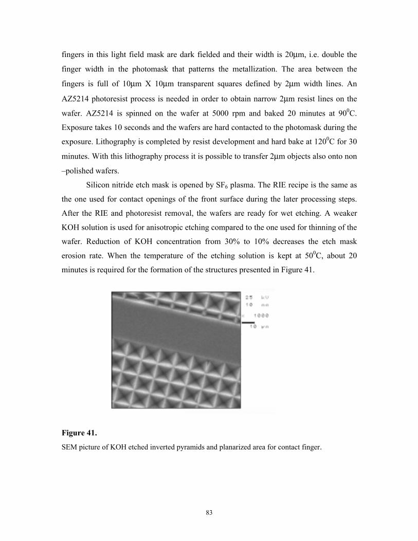
83
fingers in this light field mask are dark fielded and their width is 20µm, i.e. double the
finger width in the photomask that patterns the metallization. The area between the
fingers is full of 10µm X 10µm transparent squares defined by 2µm width lines. An
AZ5214 photoresist process is needed in order to obtain narrow 2µm resist lines on the
wafer. AZ5214 is spinned on the wafer at 5000 rpm and baked 20 minutes at 900C.
Exposure takes 10 seconds and the wafers are hard contacted to the photomask during the
exposure. Lithography is completed by resist development and hard bake at 1200C for 30
minutes. With this lithography process it is possible to transfer 2µm objects also onto non
–polished wafers.
Silicon nitride etch mask is opened by SF6 plasma. The RIE recipe is the same as
the one used for contact openings of the front surface during the later processing steps.
After the RIE and photoresist removal, the wafers are ready for wet etching. A weaker
KOH solution is used for anisotropic etching compared to the one used for thinning of the
wafer. Reduction of KOH concentration from 30% to 10% decreases the etch mask
erosion rate. When the temperature of the etching solution is kept at 500C, about 20
minutes is required for the formation of the structures presented in Figure 41.
Figure 41.
SEM picture of KOH etched inverted pyramids and planarized area for contact finger.
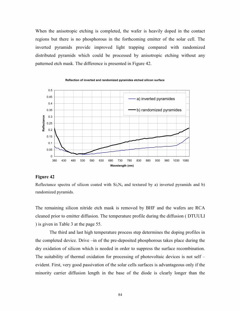
84
When the anisotropic etching is completed, the wafer is heavily doped in the contact
regions but there is no phosphorous in the forthcoming emitter of the solar cell. The
inverted pyramids provide improved light trapping compared with randomized
distributed pyramids which could be processed by anisotropic etching without any
patterned etch mask. The difference is presented in Figure 42.
Reflection of inverted and randomized pyramides etched silicon surface
0
0.05
0.1
0.15
0.2
0.25
0.3
0.35
0.4
0.45
0.5
380 430 480 530 580 630 680 730 780 830 880 930 980 1030 1080
Wavelength (nm)
Ref
lect
ance
a) inverted pyramides
b) randomized pyramides
Figure 42 Reflectance spectra of silicon coated with Si3N4 and textured by a) inverted pyramids and b)
randomized pyramids.
The remaining silicon nitride etch mask is removed by BHF and the wafers are RCA
cleaned prior to emitter diffusion. The temperature profile during the diffusion ( DTUULI
) is given in Table 3 at the page 55.
The third and last high temperature process step determines the doping profiles in
the completed device. Drive –in of the pre-deposited phosphorous takes place during the
dry oxidation of silicon which is needed in order to suppress the surface recombination.
The suitability of thermal oxidation for processing of photovoltaic devices is not self –
evident. First, very good passivation of the solar cells surfaces is advantageous only if the
minority carrier diffusion length in the base of the diode is clearly longer than the
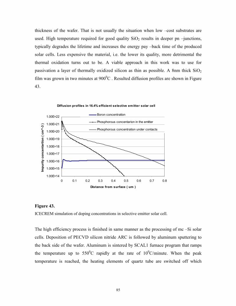
85
thickness of the wafer. That is not usually the situation when low –cost substrates are
used. High temperature required for good quality SiO2 results in deeper pn –junctions,
typically degrades the lifetime and increases the energy pay –back time of the produced
solar cells. Less expensive the material, i.e. the lower its quality, more detrimental the
thermal oxidation turns out to be. A viable approach in this work was to use for
passivation a layer of thermally oxidized silicon as thin as possible. A 8nm thick SiO2
film was grown in two minutes at 9000C . Resulted diffusion profiles are shown in Figure
43.
Figure 43. ICECREM simulation of doping concentrations in selective emitter solar cell.
The high efficiency process is finished in same manner as the processing of mc –Si solar
cells. Deposition of PECVD silicon nitride ARC is followed by aluminum sputtering to
the back side of the wafer. Aluminum is sintered by SCAL1 furnace program that ramps
the temperature up to 5500C rapidly at the rate of 100C/minute. When the peak
temperature is reached, the heating elements of quartz tube are switched off which
Diffusion profiles in 16.4% efficient selective emitter solar cell
1.00E+14
1.00E+15
1.00E+16
1.00E+17
1.00E+18
1.00E+19
1.00E+20
1.00E+21
1.00E+22
0 0.1 0.2 0.3 0.4 0.5 0.6 0.7 0.8
Distance from surface ( um )
Impu
rity
conc
enta
rtio
n ( c
m^-
3 )
Boron concentration
Phosphorous concentarion in the emitter
Phosphorous concentration under contacts

86
provide a ramp down rate of approximately 40C/minute. The front contact grid is
processed by Cr/Cu sputtering, lift off and electroplating of copper.
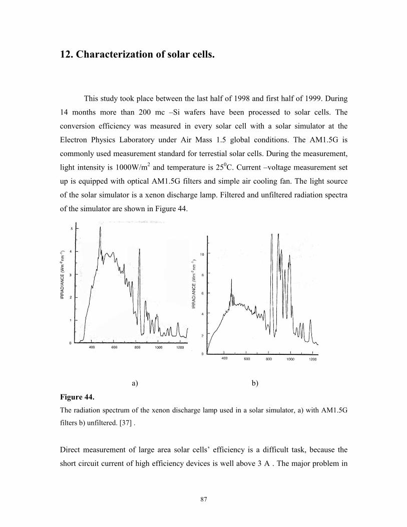
87
12. Characterization of solar cells.
This study took place between the last half of 1998 and first half of 1999. During
14 months more than 200 mc –Si wafers have been processed to solar cells. The
conversion efficiency was measured in every solar cell with a solar simulator at the
Electron Physics Laboratory under Air Mass 1.5 global conditions. The AM1.5G is
commonly used measurement standard for terrestial solar cells. During the measurement,
light intensity is 1000W/m2 and temperature is 250C. Current –voltage measurement set
up is equipped with optical AM1.5G filters and simple air cooling fan. The light source
of the solar simulator is a xenon discharge lamp. Filtered and unfiltered radiation spectra
of the simulator are shown in Figure 44.
a) b)
Figure 44. The radiation spectrum of the xenon discharge lamp used in a solar simulator, a) with AM1.5G
filters b) unfiltered. [37] .
Direct measurement of large area solar cells’ efficiency is a difficult task, because the
short circuit current of high efficiency devices is well above 3 A . The major problem in

88
accurate measurements is, however, sample heating. It is unavoidable because under the
standard measurement conditions, the solar cell is exposed to 10 W of optical power. In a
fortunate case, almost 15 percent of this radiation is converted into electricity. Since
about 1 W of the radiating power is reflected backwards, the solar cell is heated by about
7,5 W. Despite of air cooling, the temperature of the device usually increases above 250C
to some extent. Sample heating decreases the open circuit voltage because exponential
dependence on the intrinsic carrier concentration, which in turn increases the dark
saturation current of the pn –junction. For silicon, the temperature dependence of Voc is
about –2,3 mV/C0 [38]. According to independently confirmed measurements of open
circuit voltage, it can be concluded that at the Electron Physics Laboratory's air cooled
measurement unit the actual solar cells temperature during the measurement is 280C or
more.
An additional difficulty in the actual determination of the conversion efficiency is
found at the inhomogeneous intensity distribution of the xenon lamp. This can lead to an
overestimation of the output current, especially in the case of large area multicrystalline
devices which typically have local deviations of output current as shown in Figure 32. In
order to minimize the possible inaccuracies , the solar simulator was calibrated prior to
every measurement by a reference solar cell. The efficiency of the reference cell is 13,9%
which has been independently confirmed by the PV Calibration Laboratory of Fraunhofer
Institute for Solar Energy. The discharge lamp of the solar simulator was allowed to
stabilize at least for ten minutes prior to the calibration measurement. The current
potentiometer of the simulator power source was adjusted until the short circuit current of
the reference cell was the specified 3.14 A.
Most interesting samples were subjected to LBIC ( Laser Beam Induced Current )
mapping with a lifetime scanner and spectral response measurements. LBIC
measurement basically does not provide any analytical information, but it is a very useful
process monitor tool which can reveal processing problems. A typical processing
problem in the fabrication process described in this thesis is can be attributed to the
contact hole etching. Contact holes through silicon nitride antireflection coating need to
be opened by plasma etching because the annealed PECVD Si3N4 layer is very resistant
against HF based wet etchants. The HF etching rate of Si3N4 depends strongly on the
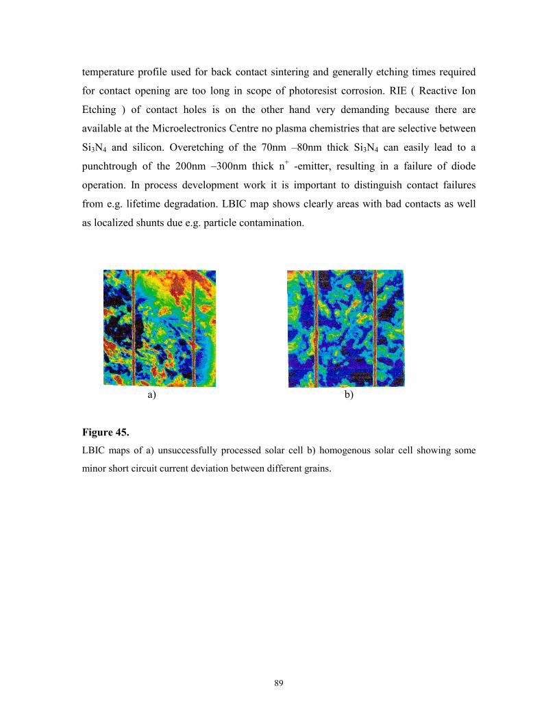
89
temperature profile used for back contact sintering and generally etching times required
for contact opening are too long in scope of photoresist corrosion. RIE ( Reactive Ion
Etching ) of contact holes is on the other hand very demanding because there are
available at the Microelectronics Centre no plasma chemistries that are selective between
Si3N4 and silicon. Overetching of the 70nm –80nm thick Si3N4 can easily lead to a
punchtrough of the 200nm –300nm thick n+ -emitter, resulting in a failure of diode
operation. In process development work it is important to distinguish contact failures
from e.g. lifetime degradation. LBIC map shows clearly areas with bad contacts as well
as localized shunts due e.g. particle contamination.
a) b)
Figure 45. LBIC maps of a) unsuccessfully processed solar cell b) homogenous solar cell showing some
minor short circuit current deviation between different grains.
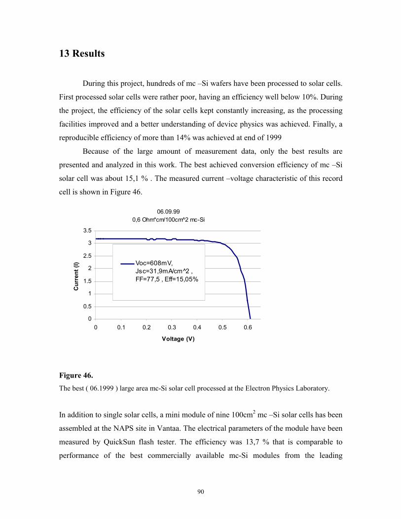
90
13 Results
During this project, hundreds of mc –Si wafers have been processed to solar cells.
First processed solar cells were rather poor, having an efficiency well below 10%. During
the project, the efficiency of the solar cells kept constantly increasing, as the processing
facilities improved and a better understanding of device physics was achieved. Finally, a
reproducible efficiency of more than 14% was achieved at end of 1999
Because of the large amount of measurement data, only the best results are
presented and analyzed in this work. The best achieved conversion efficiency of mc –Si
solar cell was about 15,1 % . The measured current –voltage characteristic of this record
cell is shown in Figure 46.
Figure 46. The best ( 06.1999 ) large area mc-Si solar cell processed at the Electron Physics Laboratory.
In addition to single solar cells, a mini module of nine 100cm2 mc –Si solar cells has been
assembled at the NAPS site in Vantaa. The electrical parameters of the module have been
measured by QuickSun flash tester. The efficiency was 13,7 % that is comparable to
performance of the best commercially available mc-Si modules from the leading
06.09.990,6 Ohm*cm/100cm^2 mc-Si
0
0.5
1
1.5
2
2.5
3
3.5
0 0.1 0.2 0.3 0.4 0.5 0.6
Voltage (V)
Cur
rent
(I) Voc=608mV,
Jsc=31,9mA/cm^2 ,FF=77,5 , Eff=15,05%

91
manufacturers. Through the module assembly, also the functionality of chromium
diffusion barrier against copper has been experimentally tested. Thin chromium barrier
prevented copper diffusion into silicon during the soldering of the module current
collection wires. This results was expected according to the studies published in
Reference [ 39 ]
13.1 Comparison of measured and simulated parameters
The exact determination of solar cells conversion efficiency is not always
straightforward. As a matter of fact, record efficiencies are claimed to be achieved and
results based on large measurement errors have been published in well –recognized
scientific journals. Afterwards these results have turned out to be false and the authors
have been subjected to severe criticism [40], [41] and [42].
In order to eliminate the possibility of misleading conclusions about the
performance of the fabrication process, it is advantageous to compare the measured solar
cells parameters with the results given by device simulator. Although the one
dimensional device simulators do not reveal the absolute truth about the solar cells
electrical parameters, the numerical calculations are based on the continuity equations of
semiconductors. Based on fundamental physics, the PC1D simulation software gives a
fast and often very accurate prediction about the efficiency of the device of interest.
Comparison of measured and PC1D simulation results as well as relevant
simulation parameters are listed in Tables 5 and 6.
Table 5. Summary of the best measured results ( bold and grey background ) and their simulated
equivalents.
Open Circuit Voltage (mV) Short Circuit Current (mA/cm2) Fill Factor (%) Efficiency (%)
measured 608 31,9 77,5 15,05 mc-Si
(100cm2) simulated 613 31,3 78,0 15,0
measured 615 34,6 77,0 16,4
92
c-Si (78cm2)
simulated 617 33,7 78,0 16,3
measured 590 32,2 77,0 14,5 RTP mc-Si
(100cm2) simulated 586 32,1 77,0 14,5
Table 6.
PC1D simulation parameters for the best mc-Si, c-Si and RTP mc –Si solar cells.
mc-Si c-Si RTP mc-Si
Thickness 300µµµµm 275µµµµm 300µµµµm
Base resistivity 0,6ΩΩΩΩ*cm 1,0ΩΩΩΩ*cm 1,5ΩΩΩΩ*cm
Shadowed area 5,25% 5,25% 5,25%
Emitter sheet resistance 43ΩΩΩΩ/sqr 40ΩΩΩΩ/sqr 100ΩΩΩΩ/sqr
Pn –junction depth 0,26µµµµm 0,87µµµµm 0,20µµµµm
Front surface recombination
velocity
100cm/s 10cm/s 100cm/s
Rear surface recombination
velocity
10000cm/s 10000cm/s 10000cm/s
Minority carrier diffusion
length 150µµµµm 350µµµµm 110µµµµm
Front surface barrier 0,1eV 0,01eV 0,1eV
Front contact series
resistance 1mΩΩΩΩ 1mΩΩΩΩ 1mΩΩΩΩ
Back contact series
resistance 1µµµµΩΩΩΩ 1µµµµΩΩΩΩ 1µµµµΩΩΩΩ
Shunt resistance 3,3ΩΩΩΩ 3,7ΩΩΩΩ 2,86ΩΩΩΩ
Reflectance data file Smc54_3r.ref Invp.txt Smc54_3r.ref

93
An important contributor to the conversion efficiency is the reflectivity of the front
surface. The reflectance data used in the PC1D simulations presented above are based on
the measured integrated reflectances. The Figure 47. visualizes the difference in the
reflection properties of differently processed silicon surfaces.
Figure 47. Reflectance spectra measured with an integrating sphere; a) smc54_3r.ref ( measured by M.Sc
Teemu Marjamäki ) was used for mc-Si and RTP mc-Si cells b) invp.txt ( measured by M.Sc
Vesa-Pekka Lempinen )was used for simulation of c-Si solar cell
As it can be seen in Table 6. , the conversion efficiencies of three differently realized
solar cell categories are within two percent. The efficiency deviation between process
technologies is essentially the same when the best results or average values of a larger
batch are compared. If the average efficiency of cells made in the same process batch is
calculated, the result is typically one percent below the record efficiency. That can be
easily explained by the irreproducibility of the non –automated and partially obsolete
process equipments as well as deviations in starting material quality.
Reflectance data used in PC1D simulations
0
0.1
0.2
0.3
0.4
0.5
0.6
0.7
0.8
300 400 500 600 700 800 900 1000 1100
Wavelenght (nm)
Ref
lect
ance
a) smc54_3r.refb) invp.txt

94
As expected, the best result for a large area silicon solar cell is obtained from a
device which is processed on the single crystalline substrate. The 1,5 % efficiency gap
between c-Si and mc-Si cells is principally a result of better silicon material purity,
higher current gain due to the inverted pyramid texturation and the very low surface
recombination velocity realized by thermal oxidation of silicon. The current gain
enhancement through the advanced light trapping structures is visualized in Figure 48.
Figure 48. PC1D simulated influence of different front surface texturation on the short circuit current of mc-
Si solar cell. The device parameters are shown in Table 6. The short circuit current density is a)
31,1 mA/cm2 b) 31,6 mA/cm2 and c) 33,0 mA/cm2
The lower efficiency of RTP mc-Si cell in contrast to conventionally processed mc-Si
device is explained by the lower minority carrier lifetime. According to the µPCD
measurements, only a slight improvement in lifetime could be achieved by rapid
processing. As described in Chapter 7, it is possible to increase significantly the lifetime
Simulated IV-curves of differently textured mc-Si solar cells
00.20.40.60.8
11.21.41.61.8
22.22.42.62.8
33.23.4
-0.1 0 0.1 0.2 0.3 0.4 0.5 0.6
Voltage (V)
Cur
rent
(A) a) SiN coated mc-Si
surface
b) randomizedpyramide textured
c) inverted pyramidetextured
95
by slow cooling of the silicon wafer after the phosphorous diffusion. The RTP technology
does not offer this advantage and the lifetime remains essentially the same as in a non –
processed mc –Si substrate which is typically from two to ten microseconds depending
on the success during the direct solidification. The emitter is, however, very shallow in
RTP cells. The shallow pn –junction compensates to some extent the effects caused by
the low lifetime, and short circuit current densities above 32 mA/cm2 were measured on a
regular basis from the RTP solar cells.
The open circuit voltage is 18mV lower in the RTP mc- Si cells in contrast to
conventionally processed device and 25mV lower compared to the c-Si one. According to
Eq. (22), the open circuit voltage of successfully processed, non –leaking solar cell is
practically determined by the diffusion length of the minority carries in base and by the
acceptor doping density of solar cells base. The effect of base doping can clearly be seen
in the measurement results presented in Table 7. A base resistivity of 1,5 Ω*cm gives a
Voc of 590mV, whereas 608 mV is measured from a cell made of 0,6 Ω*cm silicon wafer.
Similar behavior of Voc was observed in numerous measurements.
Table 7 Effect of the substrates resistivity on the solar cells performance. The solar cells measured on 5th
of May are made of same block casted multicrystalline ingot as the 15,1% efficient device.
Date/resistivity of
mc-si ingot
Voc (mV) Jsc (mA/cm2) FF (%) Eff (%)
5. May 2000 0,6 Ω*cm
602 31,2 75 14,1 5. May 2000
0,6 Ω*cm 602 30,3 76 14,0
5. May 2000 0,6 Ω*cm
602 29,8 76 13,6 5. May 2000
0,6 Ω*cm 601 31,4 73 13,7
7.September 2000 1,5 Ω*cm
584 31,8 76 14,1 7.September 2000
1,5 Ω*cm 589 32,1 74,5 14,1
7.September 2000 1,5 Ω*cm
588 32,0 74,5 14,0 7.September 2000
1,5 Ω*cm 589 31,3 75,5 13,9
2. August 2000 1,0-2,0 Ω*cm
572 32,1 75,5 13,9 2. August 2000 1,0-2,0 Ω*cm
577 32,3 74 13,8
96
2. August 2000 1,0-2,0 Ω*cm
578 32,4 75 14,0 2. August 2000 1,0-2,0 Ω*cm
576 32,1 71,5 13,2
The solar cell batches measured on 2nd of August and 7th of September are made of
substrates cut from different ingots. Processing of these batches has been essentially the
same, furnace recipe D3GET and Filmtronics P507 SOD for the diffusion. Although the
nominal resistivity is the same, 1,5 Ω*cm, it can be seen that Voc differs approximately
10mV between the batches. This 10mV deviation is apparently due to the inhomogeneous
resistivity distribution in the block casted ingots. This represents a typical fluctuation in
material quality of multicrystalline wafers. As a matter of fact, the wafer manufacturers
usually report the range of the resistivity, e.g 1,0 –2,0 Ω*cm . Low open circuit voltage
of the 2nd August batch gives the reason to believe that the resistivity of these wafers is
closer to 2,0 Ω*cm than 1,0 Ω*cm. It is also worthwhile to observe in the Table 8. the
trend of increasing current with respect to the decreasing open circuit voltage. This trend
is caused by the well –known fact that the lifetime decreases with respect to increasing
boron doping density. [43]
The opposite dependence on the resistivity of the open circuit voltage against the
short circuit current density gives rise to the conclusion that there is an optimal wafer
resistivity between 0,5 Ω*cm and 2,0 Ω*cm. Table 8 summarizes the results of the solar
cells processed differently but having the same substrate properties.
Table 8. List of solar cells electrical parameters. It is characteristic for a successful process batch that the
range of fluctuation of the results is small.
Diffusion/Al-
sintering recipes
Voc (mV) Jsc (mA/cm2) FF (%) Eff (%)
D2GET/ BSF800
594 32,4 77 14,8 D2GET/ BSF800
590 31,9 76,5 14,5 D4GET/ BSF800
592 31,5 78 14,5 D4GET/ BSF800
589 31,8 76 14,3

97
D3GET/ BSF800
592 32,5 76,5 14,8 D3GET/ BSF800
593 32,5 77 14,8 D3GET/ SCAL1
594 32,0 78,5 14,9 D3GET/ SCAL1
594 32,4 76 14,7 D4GET/ SCAL1
591 30,8 75 13,7
98
14 Conclusions
The highest experimentally demonstrated conversion efficiency of a silicon solar
cell is 24,4% . This solar cell has been fabricated at the University of New South Wales
by M.A. Green et al and it has been reported in many contents in the 1990's . The process
sequence for highest efficiency includes five high temperature oxidations, four other
furnace steps and six photolithography process steps of which five require mask
alignments. This world record solar cell has been processed from Fz –silicon ( Float Zone
) wafer and area of the device is only 4 cm2 . The highest efficiency obtained with Cz –
silicon is almost three percent lower than the record efficiency with Fz material [44].
Lower efficiency of solar cells processed from Cz –Si wafers is most likely due to
sensitivity of Cz material to the lifetime degradation during several high temperature
thermal oxidations. The essential difference between high quality Cz and Fz wafers lies
in the oxygen and carbon concentrations. Czochralski wafers always contain oxygen with
concentration that can exceed several ppm's ( parts per million ) when float zone wafers
can be fabricated to be almost free of oxygen. Because of highest quality starting material
and extremely demanding fabrication process, it is clear that these record devices are
ment to be only academic experiments that provide valuable information on fundamental
efficiency limits and device physics.
The highest conversion efficiency of a large area multicrystalline silicon solar cell
has been reported by Kyocera Ltd. to be 17,4 % [45]. Fabrication process of that solar
cell is very similar to the record single crystalline devices. The essential difference is
front surface texturation. The record mc-Si solar cell has been textured by RIE because
multicrystalline material cannot be anisotropically etched like (100) orientated single
crystalline material. Device configuration is shown in Figure 49.
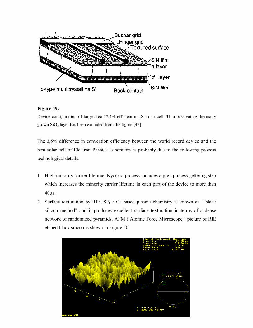
99
Figure 49. Device configuration of large area 17,4% efficient mc-Si solar cell. Thin passivating thermally
grown SiO2 layer has been excluded from the figure [42].
The 3,5% difference in conversion efficiency between the world record device and the
best solar cell of Electron Physics Laboratory is probably due to the following process
technological details:
1. High minority carrier lifetime. Kyocera process includes a pre –process gettering step
which increases the minority carrier lifetime in each part of the device to more than
40µs.
2. Surface texturation by RIE. SF6 / O2 based plasma chemistry is known as " black
silicon method" and it produces excellent surface texturation in terms of a dense
network of randomized pyramids. AFM ( Atomic Force Microscope ) picture of RIE
etched black silicon is shown in Figure 50.
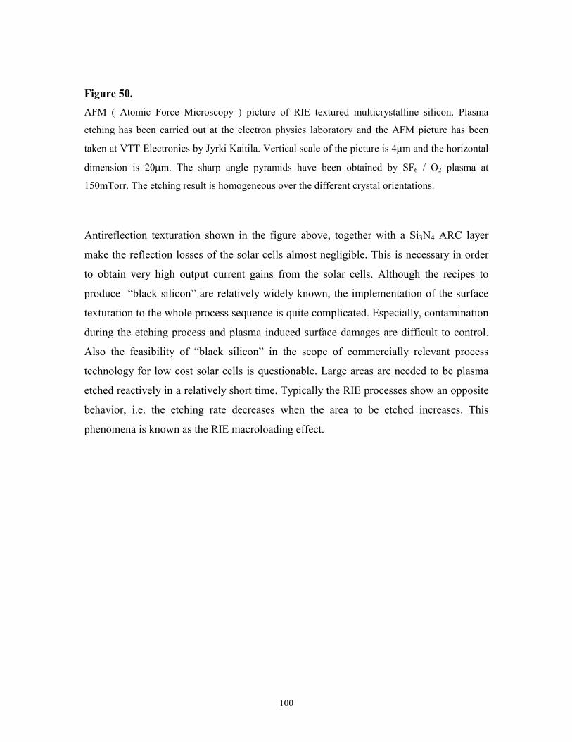
100
Figure 50. AFM ( Atomic Force Microscopy ) picture of RIE textured multicrystalline silicon. Plasma
etching has been carried out at the electron physics laboratory and the AFM picture has been
taken at VTT Electronics by Jyrki Kaitila. Vertical scale of the picture is 4µm and the horizontal
dimension is 20µm. The sharp angle pyramids have been obtained by SF6 / O2 plasma at
150mTorr. The etching result is homogeneous over the different crystal orientations.
Antireflection texturation shown in the figure above, together with a Si3N4 ARC layer
make the reflection losses of the solar cells almost negligible. This is necessary in order
to obtain very high output current gains from the solar cells. Although the recipes to
produce “black silicon” are relatively widely known, the implementation of the surface
texturation to the whole process sequence is quite complicated. Especially, contamination
during the etching process and plasma induced surface damages are difficult to control.
Also the feasibility of “black silicon” in the scope of commercially relevant process
technology for low cost solar cells is questionable. Large areas are needed to be plasma
etched reactively in a relatively short time. Typically the RIE processes show an opposite
behavior, i.e. the etching rate decreases when the area to be etched increases. This
phenomena is known as the RIE macroloading effect.

101
IQE's of textured and non textured solar cells
0
10
20
30
40
50
60
70
80
90
100
400.00 500.00 600.00 700.00 800.00 900.00 1000.00 1100.00
Wavelenght (nm)
IQE
non -textured IQE
Texture depth 9um
Texture depth 1um
Figure 51. Effect of surface texturation to the quantum efficiency. At the long wavelengths the response
seems to increase with increasing texturation depth. That increase is actually not involved with
internal quantum efficiency but rather with external quantum efficiency. PC1D simulation ,
however, is carried out with a separate data file, based on a measurement with an integrating ball,
for front surface reflectance. Therefore texturation effects become apparent in IQE simulation.
3. Electrical passivation of the front surface. Thermal oxidation of mc-Si solar cell, is
difficult to implement in the fabrication process, because of the high temperature
required. Multicrystalline material, with its high concentration of defects and impurities,
tends to degrade at the high temperatures required for high quality SiO2 passivation. An
additional detrimental effect is the drive –in of phosphorous during the oxidation which
leads to a deeper pn –junction and reduced output current. One possibility to carry out
SiO2 passivation of mc-Si solar cells is to use RTO ( Rapid Thermal Oxidation ) which
allows to grown thin oxide in about 20 seconds. In this case, the oxidation time is so short
that external contamination and phosphorous drive in do not significantly degrade solar
cells.
102
4. Selective emitter which means that under the contact fingers there is heavier doping
than in active device regions. Benefits are obtained in lower contact resistance and
reduced high doping effects in illuminated emitter region. Unfortunately formation of
selective emitter requires photolithography with mask alignment and it is therefore
excluded from low –cost processes.
5. Boron diffused Localized Back Surface Field ( LBSF ). This concept combines the
benefits of BSF and back surface passivation by thermal oxidation. Some minor
improvement can be obtained by enhanced long wavelength response, because
Si/SiO2 structure is very efficient mirror for photons that would otherwise pass
through the solar cell. Formation of LBSF require photolithography with mask
alignment and an additional masking by thermal oxidation.
There are only few reports on Rapid Thermal Processed large area solar cells processed
on multicrystalline substrates. There seems to be a clear 4-5% efficiency gap between 4
cm2 solar cells compared to any low cost, large area concepts .[47] . In the Reference [48]
a RTP based fabrication process of large area mc-Si has been reported. The results of this
IMEC group are similar to those presented in this work [33]. The efficiency of their RTP
solar cells is reported to be 14-14,8% . The minority carrier lifetime, measured by µPCD
method, is however significantly higher in the wafers used in that study [45]. The lifetime
in unprocessed mc-Si wafers used in this work is typically 2-6µs in contrast to IMEC’s
report which claims that the starting level is 25-30µs, and our low values were not
essentially improved during the processing of the solar cells. It is therefore reasonable to
conclude that the benefits of RTP technology are advantageous only when a relatively
high quality starting material, namely Cz-grown silicon, Fz-Si or mc-Si with low
impurity concentration, is used.

103
References
1. International Energy Agency. Report IEA PVPS 1-06, 1998.
2. "Crystalline Silicon Solar Cells", A. Goetzenberger, J. Knobloch and B. Voss, page
89.
3. "Operating Principles and System Applications". M.A.Green. Solar Cells , 1992
Page.10.
4. "Physics of Semiconductor Devices". S.M. Sze. 2nd Edition. 1981.
5. "Crystalline Silicon Solar Cells", A. Goetzenberger, J. Knobloch and B. Voss, page
69.
6. M.A.Green and M.J. Keevers. Progress in Photovoltaics 3, 1995 , p189.
7. "Characterization of Semiconductor Devices". D.K. Schröder.
8. " The Electrical Characterization of Semiconductors: Measurement of Minority
Carrier Properties". J.W. Orton and P. Blood.
9. "19,8% efficient "honeycomb" textured mc-Si and 24,4% c-Si solar cells". J.Zhao,
A.Wang, M.A.Green. Applied Physics Letters, vol 73, #14,1998.
10. M. Tilli. Okmetic Ltd. Personal communication.
11. "Cost Effective Solar Silicon Technology". E.Ferraza. Proceedings of 2nd World
Conference on Photovoltaic Energy Conversion. Page 1220. (1998).
12. " Influence of metal impurities on lifetime ". M. Miyazaki, et al . Sumitomo Sitix inc.
Proceedings of GADEST'97. Gettering and Defect Engineering in Semiconductor
Technology. Solid State Phenomena, Vol 57-58. 1997.
13. " Problems with Comparing µPCD and SPV Techniques" . T. Pavelka. Proceedings
of GADEST'97. Gettering and Defect Engineering in Semiconductor Technology.
Solid State Phenomena, Vol 57-58. 1997.
14. T.Suntola. Microchemistry Ltd. "Solar Energy-Dream or a Necessity".
15. W.Kern. "Handbook of Semiconductor Wafer Cleaning Technology". Page 18.
16. E.Lignell, M. Leppihalme. " Wet Etching of Poly-Si with Reference to Photovoltaic
Structures". Proceedings of 5th European Photovoltaic Solar Energy Conference. Page
1048. ( 1983 ).
17. C.Y. Chang and S.M. Sze. " ULSI Technology". Page 64.

104
18. S. Schwartzman, A. Mayer and W. Kern. " Megasonic Particle Removal from Solid –
State Wafers ". RCA review 46 , 81 (1985 ).
19. "Crystalline Silicon Solar Cells", A. Goetzenberger, J. Knobloch and B. Voss, page
95 .
20. M. Rajatora, Fortum Surface Chemistry, personal communication.
21. S.R.Wenham, L.M.Koschier and M.A. Green. " Thyristor Structure Solar Cells ".
Proceedings of 2nd World Conference on Photovoltaic Energy Conversion. 1998 . ).
22. R.B.Fair and S.C. Tsai, Journal of Electrochemical Society. 127, page 1107. 1977 )
23. J. Härkönen, V-P. Lempinen, J. Kylmäluoma, M. Rajatora and T. Mäkelä. " Large
area mc-Si solar cells with chromium copper contacts " . Proceedings of 16th
European Photovoltaic Specialist Conference.( 2001 )
24. “Modeling of gettering of precipitated impurities from Si for carrier lifetime
improvement in solar cell applications " P. S. Plekhakov, R. Gafiteanu, U. M. Gösele
and T. Y. Tan., Applied Physics Letters 86, No. 5 (1999). 2453.
25. "Formation and annihilation of oxygen donors in multicrystalline silicon for solar
cells." C. Hässler, H-U. Höfs, W. Koch, G. Stollwerck, A. Müller, D. Karg and G.
Pensl. Materials Science and Engineering B71 (2000) 39-46.
26. “Defects in multicrystalline silicon." R. Schindler and A. Räuber. Solid State
Phenomena. Vol 19&20. (1991). 341-352.
27. M.A.Green. Solar Cells: Operating Principles and System Applications. Page 151.
28. "Crystalline Silicon Solar Cells", A. Goetzenberger, J. Knobloch and B. Voss, page
151 .
29. R. Chow, W.A. Langford, W. Ke –Ming and R.S. Rosler. Journal of Applied
Physics. 53, pp.5630. (1982)
30. "Handbook of Deposition Technologies for Films and coatings". R.F.Bunshah. Noyes
Publications
31. J. Härkönen, M. Yli-Koski, E. Tuominen, Y. Ezer, V. Sokolov, J. Sinkkonen, T.
Marjamäki, and J. Kaitila. ”Silicon Solar Cells with Chromium Copper Contact”.
Proc. of 26th IEEE Photovoltaic Specialists Conference. (1997 )
32. P.Doshi, J. Mejia, K. Tate,S. Kamra, A. Rohatgi, R, Singh and S.Narayanan. “High
efficiency silicon solar cells by low-cost rapid thermal processing, screen printing
105
and PECVD “. Proceedinds of 25th IEEE Photovoltaic Specialist Conference, page
421. 1996
33. V.E. Borisenk and P.J. Hesketh. ”Rapid Thermal Processing of Semiconductors”.
Plenum Publishing Corp. Series of Microdevices. New York. 1997.
34. K. Solehmainen. “Rapid Thermal Processing of multicrystalline silicon solar cells”.
Master’s Thesis. Helsinki University of Technology. Electron Physics Laboratory.
2000
35. “Handbook of Semiconductor Silicon Technology” . Edited by W. O’Mara, R.
Herring and L. Hunt. Noyes Publications. 1990.
36. T. Juvonen. “ Processing of high efficiency singlecrystalline silicon solar cells”
Master’s Thesis. Helsinki University of Technology. Electron Physics Laboratory.
2000
37. Oriel Corporation. " Solar Simulation" . Product Catalog.
38. "Operating Principles and System Applications". M.A.Green. Solar Cells , 1992
39. Y. Ezer, J. Härkönen, V. Sokolov, J. Saarilahti, J. Kaitila and P. Kuivalainen. "
Diffusion Barrier Performance of Thin Cr Films in the Cu/Cr/Si Structure ".
Materials Research Bulletin. Vol 33. No 9. Page 1331. 1998.
40. A. Rohatgi, J. Monschner and M.A.Green. ”Correspondence and comments on
17.3% Efficiency Metal-Oxide-Semiconductor (MOS) Solar Cells with Liquid Phase
Deposited Silicon Dioxide ”, IEEE Electron Device Letters. Vol 19, No. 11,
November 1998.
41. J.Li, M. Chong, J. Zhu, Y.Li, J. Xu, P.Wang, Z. Shang, Z. Yang, R.Zhu and X.Cao. ”
35% Efficient Nonconcentrating Novel Silicon Solar Cell.” Appl.Phys.Lett.,Vol 60,
p.2240, 1992
42. Commets from various authors for [38] . Appl.Phys.Lett.,Vol 63, pp.848-852, 1993
43. “Crystalline Silicon Solar Cells", A. Goetzenberger, J. Knobloch and B. Voss, page
44 .
44. "Operating Principles and System Applications". M.A.Green. Solar Cells , 1992 Page
92.

106
45. J. Knobloch, S.W.Glunz, D. Biro, W. Warta, E. Schäffer and W. Wettling. " Solar
Cells with Efficiencies above 21% Processed from Cz Grown Silicon ". Proceedings
of 25th IEEE Photovoltaic Specialist Conference, page 405. 1996.
46. K. Shirasawa, K. Fukui, K. Okada, Y. Inomata and S. Fujii. " Over 17% Large Area
Multicrystalline Silicon Solar Cells." Proceedings of 14th European Photovoltaic
Specialist Conference, page 384, 1997.
47. P.Doshi, J. Moschener, J. Jeong, A. Rohatgi, R, Singh and S.Narayanan. “
Characterization and application of rapid thermal oxide surface passivation for the
highest efficiency RTP silicon solar cells “. Proceedinds of 26th IEEE Photovoltaic
Specialist Conference, page 87. 1997
48. S.Sivoththaman, J. Horzel, F. Duerinckx, P. De Schepper, W. Laureys, J. Szlufcik, J.
Nijs and R. Mertens. “ High Throughput processing of large area mc-Si solar cells by
Rapid Thermal Processing and Screenprinting”. Proceedings of 2nd World
Conference on Photovoltaic Energy Conversion. Page 1770. 1998


