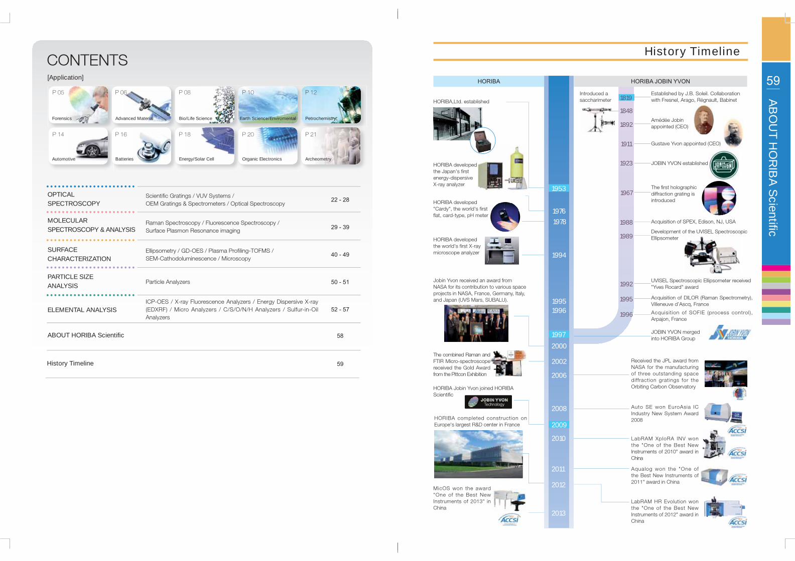
Established by J.B. Soleil. Collaboration with Fresnel, Arago, Régnault, Babinet
Introduced a saccharimeter
Acquisition of SPEX, Edison, NJ, USA
UVISEL Spectroscopic Ellipsometer received "Yves Rocard" award
Development of the UVISEL Spectroscopic Ellipsometer
The fi rst holographic diffraction grating is introduced
Acquisition of DILOR (Raman Spectrometry), Villeneuve d’Ascq, France
Acquisition of SOFIE (process control), Arpajon, France
1996
JOBIN YVON merged into HORIBA Group
HORIBA HORIBA JOBIN YVON
1819
1988
1989
1967
1923
1848
1892
1911
1992
19951995
1994
1996
2002
2006
2008
2012
2013
2011
2010
2009
1997
1953
2000
1976
1978
LabRAM XploRA INV won the "One of the Best New Instruments of 2010" award in China
HORIBA,Ltd. established
HORIBA developed the Japan's fi rst energy-dispersive X-ray analyzer
HORIBA developed "Cardy", the world's fi rst fl at, card-type, pH meter
HORIBA developed the world's fi rst X-ray microscope analyzer
Jobin Yvon received an award from NASA for its contribution to various space projects in NASA, France, Germany, Italy, and Japan (UVS Mars, SUBALU).
The combined Raman and FTIR Micro-spectroscope received the Gold Award from the Pittcon Exhibition
HORIBA Jobin Yvon joined HORIBA Scientifi c
HORIBA completed construction on Europe's largest R&D center in France
MicOS won the award "One of the Best New Instruments of 2013" in China
LabRAM HR Evolution won the "One of the Best New Instruments of 2012" award in China
Auto SE won EuroAsia IC Industry New System Award 2008
Aqualog won the "One of the Best New Instruments of 2011" award in China
Received the JPL award from NASA for the manufacturing of three outstanding space diffraction gratings for the Orbiting Carbon Observatory
ABOUT HORIBA Scientifi c
58
AB
OU
T HO
RIB
A S
cientifi c
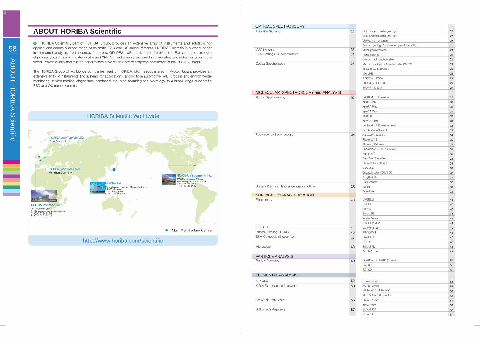
HORIBA Scientific, part of HORIBA Group, provides an extensive array of instruments and solutions for applications across a broad range of scientific R&D and QC measurements. HORIBA Scientific is a world leader in elemental analysis, fluorescence, forensics, GD-OES, ICP, particle characterization, Raman, spectroscopic ellipsometry, sulphur-in-oil, water quality and XRF. Our instruments are found in universities and industries around the world. Proven quality and trusted performance have established widespread confi dence in the HORIBA Brand.
The HORIBA Group of worldwide companies, part of HORIBA, Ltd, headquartered in Kyoto, Japan, provides an extensive array of instruments and systems for applications ranging from automotive R&D, process and environmental monitoring, in-vitro medical diagnostics, semiconductor manufacturing and metrology, to a broad range of scientifi c R&D and QC measurements.
http://www.horiba.com/scientifi c
HORIBA Scientifi c Worldwide
Main Manufacture Centre
Sulfur-in-Oil Analyzers
Ultima Expert
XGT-5200WR
MESA-50 / MESA-50K
XGT-7200V / XGT-5200
EMIA-920V2
EMGA-930
SLFA-2800
SLFA-60
LA-960 and LA-960 (Dry unit)
LA-300
SZ-100
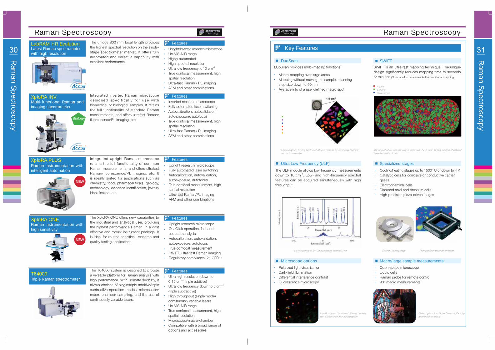
LabRAM HR Evolution
XploRA INV
XploRA Plus
XploRA One
T64000
XploRA Nano
LabRAM HR Evolution Nano
Combiscope XploRA
Aqualog® / Dual-FL
Fluorolog®-3
Fluorolog Extreme
FluoroMax®-4 / Plus (P/TCSPC)
NanoLog®
DeltaPro / DeltaFlex
FluoroCube / UltraFast
DeltaMyc
QuantaMaster 400 / 800
EasyRatioPro
RatioMaster
EzPlex
OpenPlex
UVISEL 2
UVISEL
Auto SE
Smart SE
In-situ Series
UVISEL 2 VUV
GD Profi ler 2
PP-TOFMS
Flex-CLUE
HCLUE
SmartSPM
CombiScope
Gold coated master gratings
Multi-layer dielectric gratings
VUV custom gratings
Custom gratings for astronomy and space fl ight
VUV Spectrometers
Plane gratings
Customized spectrometers
Microscope Optical Spectrometer (MicOS)
EasyLife X / EasyLife L
MicroHR
iHR320 / iHR550
FHR640 / FHR1000
1000M / 1250M
22
22
22
22
23
24
24
26
26
26
26
26
27
30
30
30
30
30
33
33
33
34
35
35
35
35
36
36
36
37
37
37
39
39
42
42
42
43
43
43
45
46
47
47
49
49
50
51
51
52
53
53
53
55
56
57
57
22
2324
25
29
34
38
40
4446
50
52
47
48
53
55
57
Scientifi c Gratings
VUV Systems
Optical Spectroscopy
Raman Spectroscopy
Surface Plasmon Resonance imaging (SPRi)
Fluorescence Spectroscopy
Ellipsometry
GD-OES
SEM-Cathodoluminescence
Microscopy
ICP-OES
X-Ray Fluorescence Analyzers
C/S/O/N/H Analyzers
Particle Analyzers
Plasma Profi ling-TOFMS
OEM Gratings & Spectrometers
OPTICAL SPECTROSCOPY
MOLECULAR SPECTROSCOPY and ANALYSIS
SURFACE CHARACTERIZATION
ELEMENTAL ANALYSIS
PARTICLE ANALYSIS
Products & Application
Measurement range: 0-9.9999 %Repeat accuracy: 15 ppm or less (with a 1 % sample)Lower detection limit: 20 ppmSample requirement: 4-10 mL Measurement time: User-set from 10 to 600 seconds
Measurement range: 0-0.999 %Repeat accuracy: 5 ppm or less (with a 1 % sample) 1.6 ppm or less (with a 0 % sample)Lower detection limit: 5 ppm or lessSample requirement: 4-10 mLMeasurement time: User-set from 10 to 600 seconds
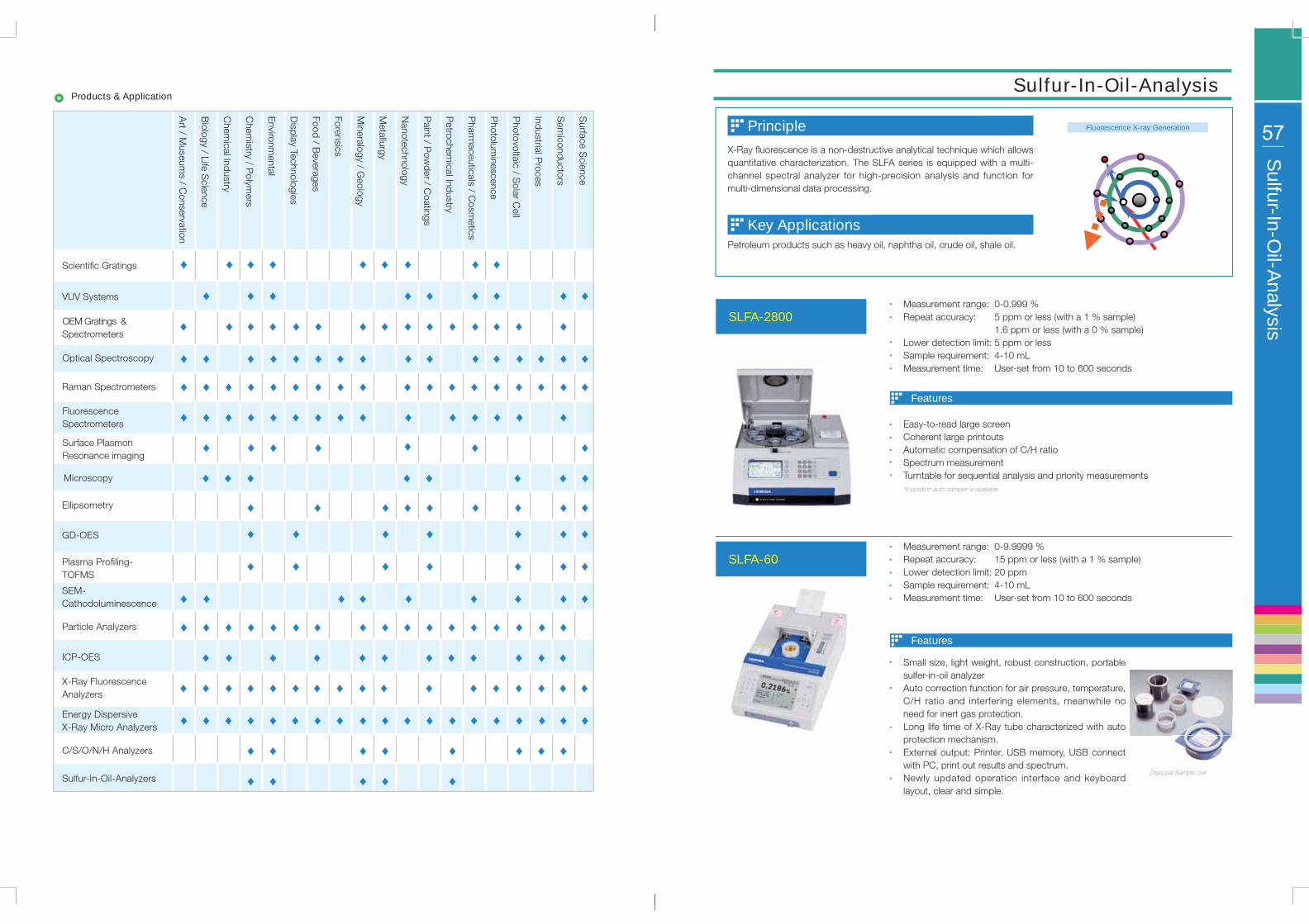
Sulfur-In-O
il-Analysis
Sulfur-In-Oil-Analysis
57
原子核
SLFA-2800
SLFA-60
Principle
Key Applications
X-Ray fl uorescence is a non-destructive analytical technique which allows quantitative characterization. The SLFA series is equipped with a multi-channel spectral analyzer for high-precision analysis and function for multi-dimensional data processing.
Petroleum products such as heavy oil, naphtha oil, crude oil, shale oil.
Features
Features
Easy-to-read large screenCoherent large printoutsAutomatic compensation of C/H ratioSpectrum measurement Turntable for sequential analysis and priority measurements*8 position auto sampler is available
Small size, light weight, robust construction, portable sulfer-in-oil analyzerAuto correction function for air pressure, temperature, C/H ratio and interfering elements, meanwhile no need for inert gas protection.Long life time of X-Ray tube characterized with auto protection mechanism.External output: Printer, USB memory, USB connect with PC, print out results and spectrum.Newly updated operation interface and keyboard layout, clear and simple.
Disposal Sample cell
Fluorescence X-ray Generation
EMGA-930Oxygen/Nitrogen/Hydrogen AnalyzerC
arbon/S
ulfur/Oxygen/N
itrogen/Hyd
rogen Analysis
56
Carbon/Sulfur/Oxygen/Nitrogen/Hydrogen Analysis
Features
Automated crucible supply system and auto cleaner achieve the full-automatic operation of EMGA.
Super high performanceUser-friendly softwareFully supported accessories offer simple operationImproved, easier to use mechanismDual Sample/Flux introduction mechanism
Measuring Range:Oxygen: 0.04 ppm-5 %Nitrogen: 0.04 ppm-3 %Hydrogen: 0.08 - 0.25 %Up to 100 % is possible by decreasing the sample weight.
Accuracy (repeatability):Oxygen/Nitrogen:SD ≦ 0.02 ppm or more RSD ≦ 0.5 % (Reference gas)HydrogenSD ≦ 0.04 ppm or more RSD ≦ 2.0 % (Reference gas)
Inert Gas Fusion in Impulse Furnace:Able to set the generating power 0-8.0 kWMaximum temperature: 3000 Celsius
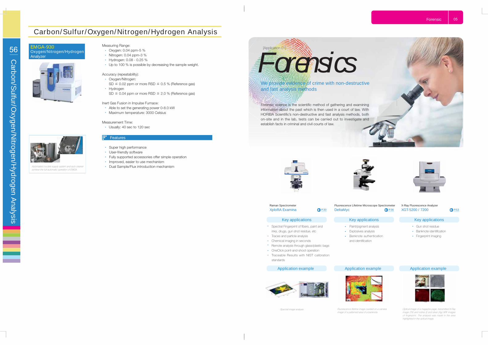
Forensic science is the scientifi c method of gathering and examining information about the past which is then used in a court of law. With HORIBA Scientifi c’s non-destructive and fast analysis methods, both on-site and in the lab, tests can be carried out to investigate and establish facts in criminal and civil courts of law.
We provide evidence of crime with non-destructive and fast analysis methods
Forensics
Key applications
Application example Application example Application example
Key applications Key applications
Gun shot residue
Banknote identifi cation
Fingerprint imaging
Paint/pigment analysis
Explosives analysis
Banknote authentication
and identifi cation
Spectral image analysis Optical image of a magazine page, transmitted X-Ray image (TX) and iodine (I) and silver (Ag) XRF images of fingerprint. The analysis was made in the area highlighted in the optical image.
Fluorescence lifetime image overlaid on a cameraimage of a patterned area of a banknote.
XploRA Nano AFM-Raman
Nanolog®Fluorescence Spectrometer
UVISEL 2Ellipsometry
P.30 P.35 P.42
AFM image Raman image
06 Advanced Material
[Application 02]
New materials such as ultra-fi ne particles, optical catalysts, hybrid materials and polymer gels are attracting the attention of research and development. In order to show the characteristics of these new materials, not only are manufacturing and forming processes important, but so are the analytical skills and analytic technologies that evaluate them. HORIBA contributes to the growth of the industry by supporting the development of cutting-edge materials based on the latest analysis systems and application development.
In the development of cutting-edge materials that attract the attention of the industry, various evaluations and analysis is required
Advanced Materials
Key applications
Application example Application example Application example
Key applications Key applications
Raman-AFM co-localization image of graphene
* Tip Enhanced Raman Spectroscopy
Micro spot on graphene with patented vision system3-D matrix of SWCNT
AFM-Raman simultaneous localization
imaging
TERS*- chemical fi ngerprint at the nanoscale
Physical property & chemical structure analysis
Nano material growth mechanism studies
Carbon nanotubes chirality and diameters
Carbon nanotubes luminescence
mechanism
Quantum dot size adjustment
Luminous effi ciency of nano-materials
Thickness, optical constants
Material / surface modifi cation
Roughness, porosity
Gradient layer, interface
Transmission, refl ectivity curve
Carb
on/Sulfur/O
xygen/Nitrogen/H
ydrogen A
nalysis
Carbon/Sulfur/Oxygen/Nitrogen/Hydrogen Analysis
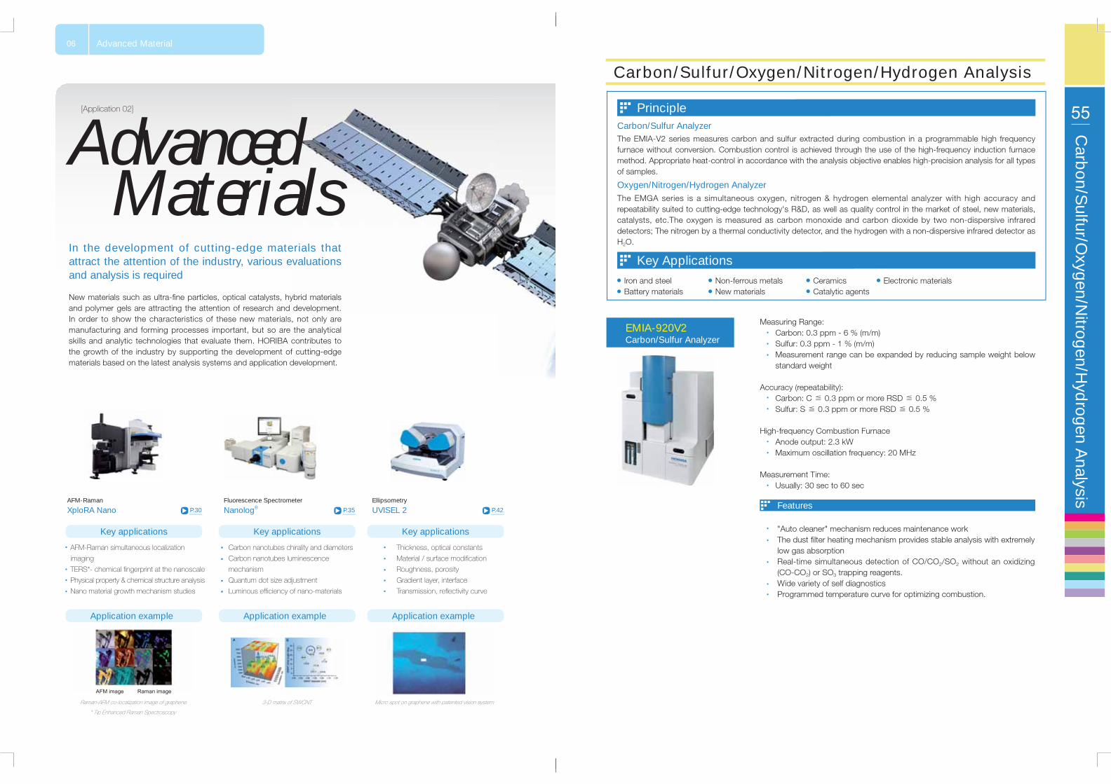
55Carbon/Sulfur AnalyzerThe EMIA-V2 series measures carbon and sulfur extracted during combustion in a programmable high frequency furnace without conversion. Combustion control is achieved through the use of the high-frequency induction furnace method. Appropriate heat-control in accordance with the analysis objective enables high-precision analysis for all types of samples.
The EMGA series is a simultaneous oxygen, nitrogen & hydrogen elemental analyzer with high accuracy and repeatability suited to cutting-edge technology's R&D, as well as quality control in the market of steel, new materials, catalysts, etc.The oxygen is measured as carbon monoxide and carbon dioxide by two non-dispersive infrared detectors; The nitrogen by a thermal conductivity detector, and the hydrogen with a non-dispersive infrared detector as H2O.
Oxygen/Nitrogen/Hydrogen Analyzer
EMIA-920V2Carbon/Sulfur Analyzer
Iron and steelBattery materials
Ceramics Electronic materialsCatalytic agents
Non-ferrous metalsNew materials
Principle
Key Applications
Features
"Auto cleaner" mechanism reduces maintenance work The dust fi lter heating mechanism provides stable analysis with extremely low gas absorption Real-time simultaneous detection of CO/CO2/SO2 without an oxidizing (CO-CO2) or SO3 trapping reagents.Wide variety of self diagnostics Programmed temperature curve for optimizing combustion.
Measuring Range:Carbon: 0.3 ppm - 6 % (m/m) Sulfur: 0.3 ppm - 1 % (m/m)Measurement range can be expanded by reducing sample weight below standard weight
Accuracy (repeatability):Carbon: C ≦ 0.3 ppm or more RSD ≦ 0.5 %Sulfur: S ≦ 0.3 ppm or more RSD ≦ 0.5 %
Optical image Analysis result with 1.2 mm Analysis result with 400 μm
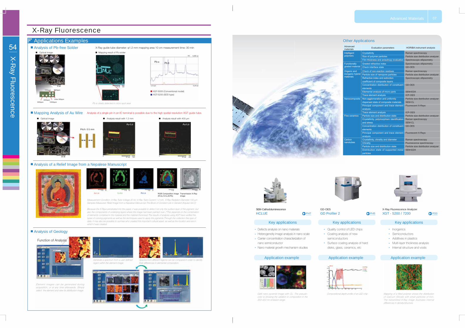
Mapping result of Pb solder
X-Ray guide tube diameter: φ1.2 mm mapping area 10 cm measurement time: 30 min
1000ppm
3000ppm
5000ppm
2000ppm10000ppm
under 500ppm
Analysis of a Relief Image from a Nepalese Manuscript
Analysis of Geology
Pb is clearly detected in micro spot area
XGT-5000 (Conventional model)XGT-5200 (SDD type)
Analysis of a single pin in an IC terminal is possible due to the high spatial resolution XGT guide tube.
Pitch: 0.5 mm
Measurement Condition: X-Ray Tube Voltage:30 kV; X-Ray Tube Current:1.0 mA; X-Ray Radiation Diameter:100 μmSamples Measured: Relief Image from a Nepalese Manuscript.The Book of Constant Life in Sanskrit (Kojukai Ver.C)
Because the X-Rays penetrated into the paper, it was possible to detect not only the surface layer of the pigment, but also the components of underlying layers where the image had been painted over. (*This depends on the combination of elements contained in the material and the material thickness) The results of analysis using XGT have verifi ed the types of coloring pigments as well as the techniques used to apply the pigments.Through the collection this type of data, it may also be possible to surmise who created this important cultural asset, as well as the location and era in which it was created.
Transmission X-Ray image
RGB Composition image(R:Au G:Cu B:Pb)
Function of Analysis
Generate a spectrum from a user defi ned region within the element image.
Spectra from different regions can be compared in order to identify their differences in elemental composition.
Element images can be generated dur ing acquisition, or at any time afterwards. SImply select the element and view its distribution image.
Applications Examples
GD Profi ler 2GD-OES
XGT - 5200 / 7200X-Ray Fluorescence Analyzer
P.47 P.45 P.53HCLUESEM-Cathodoluminescence
Other ApplicationsAdvanced materials Evaluation parameters HORIBA instrument analysis
Intelligent polymers
CrystallinitySize of polymer particlesFilm thickness and anisotropy evaluation
Raman spectroscopy Particle size distribution analyzerSpectroscopic ellipsometry
Spectroscopic ellipsometryGD-OES
Raman spectroscopy Particle size distribution analyzer Spectroscopic ellipsometry
GD-OES
SEM-EDX ICP-OES
Particle size distribution analyzerRaman spectroscopy SEM-CLGD-OES
Fluorescent X-Rays
Raman spectroscopy Fluorescence spectroscopy Particle size distribution analyzer SEM-EDX
Particle size distribution analyzerSEM-CLFluorescent X-Rays
ICP-OES
Graded refractive indexCheck interface state
Check of non-reaction residuesParticle size of nanopore particlesRefractive index and extinctioncoeffi cient of composite layers Concentration distribution of constituent elements Elemental analysis of micro parts Trace element analysisNon-agglomeration and uniformlydispersed state of composite materials Principal component and trace element analysisTrace element analysisParticle size and distribution stateCrystallinity, polymorphism identifi cation and stressConcentration distribution of constituent elements Principal component and trace element analysis Crystallinity, chirality and diameterChirality Particle size and distribution state Distribution state of supported metal particles
Functionally graded material
Nanocomposite
Fine ceramics
Carbon nanotubes
Organic and inorganic hybrid materials
07Advanced Materials
Key applications
Application example Application example Application example
Key applications Key applications
GaN nano pyramid image with CL. The pseudo-color is showing the variation in composition in the 350–450 nm emission range.
Mapping of a filled polymer shows the distribution of Calcium Silicate with small particles of Iron. The transmitted X-Ray image illustrates internal differences in density/structure.
Application example Application example Application example
Key applications Key applications
Biomacromolecule identifi cation
Bacteria, identifi cation and classifi cation
Drug distribution in cells/tissues
Early disease diagnosis
Label-free in-vivo and in-vitro analysis
Biomacromolecule conformational change
Quantifi cation of biomolecules
Enzymatic activity and cell viability
Molecular interactions
FRET
Protein aggregates
Liposomes and virus
Protein's Zeta potential
Nile Red distribution in Bovine embryo(Courtesy of Igor Chourpa, Pharmacy Faculty,University of Tours)
Measurement results of the particle size of lysozyme and isoelectric point
FLIM measurement (left, showing average lifetime) and representative decay profi les (right) from FITCBSA in and outside an irradiated area.
[Application 03]
Complex and elaborate mechanisms of l i fe phenomena that organisms perform are clarified through science and technology
Bio /Life Science
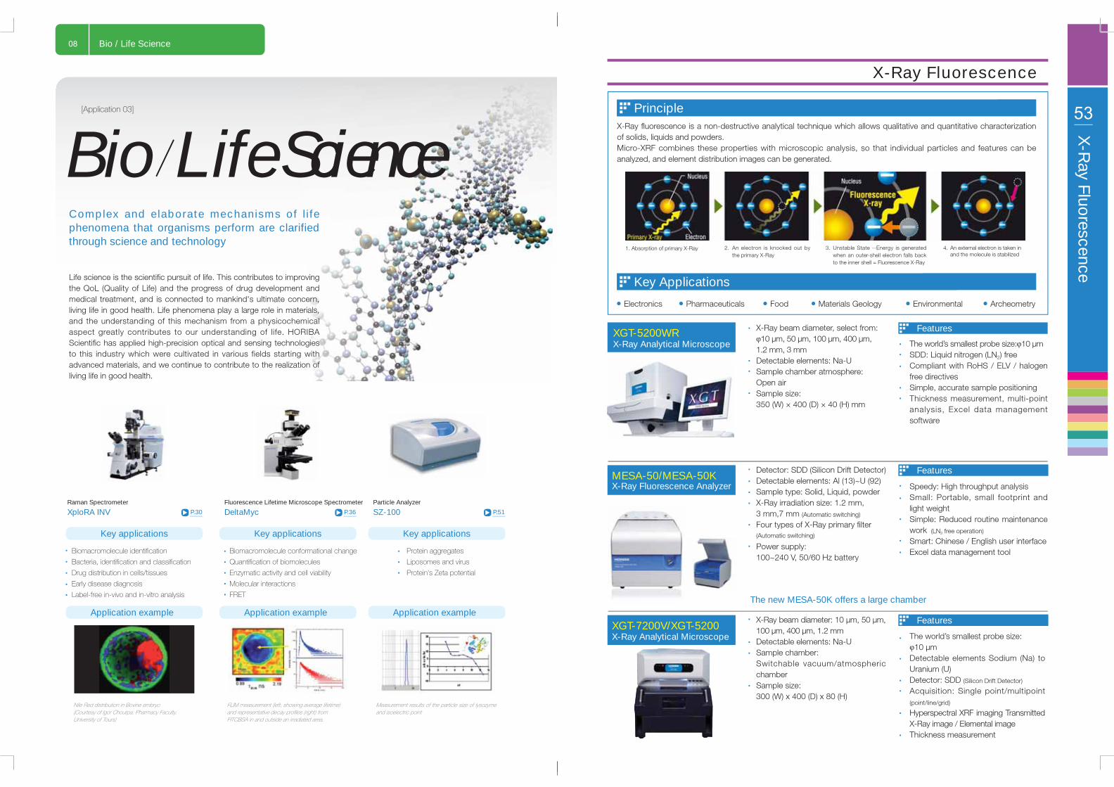
Life science is the scientifi c pursuit of life. This contributes to improving the QoL (Quality of Life) and the progress of drug development and medical treatment, and is connected to mankind's ultimate concern, living life in good health. Life phenomena play a large role in materials, and the understanding of this mechanism from a physicochemical aspect greatly contributes to our understanding of life. HORIBA Scientifi c has applied high-precision optical and sensing technologies to this industry which were cultivated in various fields starting with advanced materials, and we continue to contribute to the realization of living life in good health.
X-Ray fl uorescence is a non-destructive analytical technique which allows qualitative and quantitative characterization of solids, liquids and powders.Micro-XRF combines these properties with microscopic analysis, so that individual particles and features can be analyzed, and element distribution images can be generated.
4. An external electron is taken in and the molecule is stabilized
1. Absorption of primary X-Ray 2. An electron is knocked out by the primary X-Ray
3. Unstable State --Energy is generated when an outer-shell electron falls back to the inner shell = Fluorescence X-Ray
Features
Features
Features
X-Ray beam diameter, select from: φ10 μm, 50 μm, 100 μm, 400 μm, 1.2 mm, 3 mm Detectable elements: Na-USample chamber atmosphere: Open airSample size:350 (W) × 400 (D) × 40 (H) mm
The world’s smallest probe size:φ10 μmSDD: Liquid nitrogen (LN2) freeCompliant with RoHS / ELV / halogen free directivesSimple, accurate sample positioningThickness measurement, multi-point analysis, Excel data management software
Speedy: High throughput analysisSmall: Portable, small footprint and light weightSimple: Reduced routine maintenance work (LN2 free operation)
Smart: Chinese / English user interfaceExcel data management tool
The world’s smallest probe size:φ10 μmDetectable elements Sodium (Na) to Uranium (U)Detector: SDD (Silicon Drift Detector)
Acquisition: Single point/multipoint (point/line/grid)
Ultima Expert Unique plasma torch design offers the most versatile and accurate analysesAccessories for varied applicationsHigh resolution and full wavelength coverageEasy to handle, easy to maintain
Performance through a simplifi ed method developmentFlexibility in analysis with multiple tasks sequenceImage navigator displays the full spectra acquired and offers unique features for qualitative and semi-quantitative analysis
Simultaneous measurement of hydride and non-hydride forming elements without changing the introduction system. Easy to use.
Used in analysis of wear metal, oil, gasoline, biodiesel and suspension solution, etc.
Control sample analysis by software
Principle
Key Applications
Software
ICP-OES is an analytical technique used for the detection of trace elements. The sample is nebulized then transferred to an argon plasma. It is decomposed, atomized and ionized whereby the atoms and ions are excited. The intensity of the light emitted when the atoms or ions return to lower levels of energy is measured. Each element emits light at characteristic wavelengths and these lines can be used for quantitative or qualitative analysis.
The robustness of the Ultima Expert makes it ideal for applications common to mining, chemicals manufacture, salt production, wear metals in oil analysis, petrochemicals, metallurgical production and precious metal refi ning. Ultima Experts offers maximum effi ciency for your most demanding applications.
The analyst software package of the Ultima Expert extends instrument capability beyond analytical performance, featuring advanced user guidance from sample to results.
For elemental analysis in the presence of line-rich spectrum elements such as iron, tungsten or rare earth elements, the Ultima Expert delivers the highest performance.
Major and trace elements analysis in varying matrices along with reliability and confi dence in the fi nal results.
Ultima Expert is the only ICP-OES spectrometer on the market to provide ultimate accuracy for major precious metals analysis.
Ultima Expert is a unique combination of ultimate performance with comprehensive assistance tools designed to simplify method development. Ult ima Expert integrates our high efficiency Jobin Yvon optical design capable of achieving optimal performance for a large variety of sample types and matrices. More than 70 elements can be analyzed with ICP-OES, including Cl and Br.
Every compound has a function and a role, as do aggregates. HORIBA's technology helps to clarify the connection between these types of life phenomena (functions) and expression mechanisms.
Key applications
Application example Application example Application example
Key applications Key applications
Label-free analysis of protein and DNA
Intermolecular binding specifi city
Molecular modifi cation
Molecular dynamics analysis
Automatic biochemical analyzer
Chemiluminescence immunoassay
Real-time fl uorescence quantifi cation
The structure of macromolecules
Mechanic properties of macromolecule
Process of macromolecule activities
Cell and organelle topography
Direct comparison of binding parameters in only one experiment
Alternanthera mosaic potex virus. Sample courtesy of Prof. O. V. Karpova and Dr. M. V. Arhipenko, Lomonosov Moscow State University, Faculty of Biology
Grating effi ciency for biomed application
Life
Tissues / organs
Micro-organisms
Organelles
Compounds
Molecules
Atoms and ions
Sugars, Lipids etc.
Proteins, DNA etc.
XploRA PLUSRaman Spectrometer
P.30
CaCO3 Carbon
PbSO4/PbCO3
PbSO4/(Ca,Mn)CO3
Aqualog® / Dual-FLFluorescence Spectrometer
P.34 SZ-100Particle Analyzer
P.51
10 Earth Science / Environmental
Key applications
Application example Application example Application example
Key applications Key applications
Chemical composition of aerosols
Aerosol particles-atmospheric reaction
Polymers/organics degradation analysis
Contaminants/pesticide residue detection
Bacteria/microbiological analysis
Colored dissolved organic matter research
Disinfection by-products research
Organic pollutant analysis
Carbon migration mechanism
Analysis of suspended particles in
waste water treatment
Analysis and treatment of oil
refi nery waste water
Analysis of sediment particles
Molecular images of the lead-rich necrotic zone onthe leaf surface (Courtesy of Sophie Sobanska,University of Lille)
The relationship between the Zeta potential valueof suspended particles and the additives of wastewater treatment
3-D matrix of water sample
EnvironmentalEarth ScienceHORIBA ensures a safe living environment with multiple analysis
Our lives are affected by a variety of factors in our environment, such as the quality of food, medicines, crops, atmospheric and radioactive pollution, to name a few, all of which impact our survival.
y
[Application 04] 51
Particle Analysis
Particle A
nalysis
Fraction cell / cell holder:
Autofi ll pump:
LA-300Laser Scattering Particle Size Distribution Analyzer
Measurement Angles: 90° & 173° (automatic or manual selection)
Sample volume:12 μL to 4 ml
Measurement Principle: Laser Doppler ElectrophoresisMeasurement Range: –200 to +200 mV (no actual limits)
Sample Volume:100 μL
Measurement Principle: Debye plotMeasurement Range: 1000 to 2 ×10⁷ Da
A single device analyzes three parametersTwo angle system enables analysis of a wide range of high concentration and diluted samplesLowest sample volumeCell design minimizes EOF
Particle A
nalysis
50
Particle Analysis
Static Light Scattering (SLS)
Mini fl ow (Small volume circulation system, Solvent resistant):
LA-960Laser Scattering Particle Size Distribution Analyzer
LA-960 (Dry unit)Powder Jet Dry Feeder System
Ceramics Pigments & Inks
Cosmetics
Colloids
Pharmaceuticals
NanomaterialsBatteries
Macromolecules Nanocapsules
Principle
Key Applications
When light strikes particles, scattering (diffraction) occurs. Detectors can receive different electrical signals according to the intensity and angles of scattered light. And sample size distribution is calculated from these electrical signals based on Mie theory. Light scattering method has excellent reproducibility and accuracy.
Dynamic Light Scattering is the measurement of fl uctuations in scattered light intensity with time. These fl uctuations in intensity are due to the random Brownian motion of the nanoparticle. Since larger particles diffuse more slowly than small particles, one can readily relate particle size to measured fl uctuations in light scattering intensity. With modern instruments, the technique is rapid and reliable.
Minimize sample and dispersant volume requirements with all the convenience of a fully-automated circulation system.The software controls all sequences such as fi ll, rinse and drain; No manual operation required.
This accessory is ideal when the total sample amount is small, the sample or dispersant is toxic, or you wish to recover the measurement sample.
Features
Features
The world’s widest dynamic rangeThe world’s fastest analysisInnovative optical systemGuaranteed high data accuracy:± 0.6% and high data repeatability: ±0.1% performance with NIST-traceable standard particles down to 20 nm
Measurement Method:Mie scattered theoryMeasurement Range: 10 nm-5000 μmSample Amount: 10 mg~5 gDispersion Medium: 180 mL~250 mLMeasurement Time: 1 minute from dispersion liquid filling to measurement to rinseUltrasonic probe: 30 W (Max:130W) Frequency: 20 kHz, 7-levels selection
Automatic control of sample feeder rateQuick and easy switch between wet and dry measurementsOne instrument suits all sample requirementsInstalled on the main unit, requires no additional spaceEasy disassembly and easy maintenance
Dispersant method:Injector drive forced dispersion in airSample Supply Method: Vibrating feederMeasurement range:0.1 μm~5000 μmMeasurement time: 2 seconds from start to measurement
Accessories
Food
Catalysts
Flex-CLUESEM-Cathodoluminescence
XGT - 5200X-Ray Fluorescence Analyzer
P.47 P.53P.52Ultima Expert ICP-OES
Zircon CL Analysis Elemental and optical image of micrometeoritesOnly t race Ga wi l l a f fect the magnet ism and microstructure of NdFeB products In rare earth elements analysis: For rare earth elements, only high resolution ICP-OES can separate those spectral interferences. Left image: resolution of <5 pm. Right image: If resolution goes to about 10 pm, the Ga signal will be lost.
11Earth Science / Environmental
Key applications
Application example Application example Application example
Key applications Key applications
Identifi cation of minerals
Distribution analysis of minerals
Trace elements inside minerals
Analysis of mineral formation
Quantitative analysis of contaminants in soils
Marine/ocean sediments
Toxic element build up in tissue/cells
Airborne particles and air fi lters
Composition of minerals / rocks
Recycling materials
Rare earth elements analysis
Precious metals analysis
Alloy and mineral samples
XploRA PLUSRaman Spectrometer
Aqualog® / Dual-FLFluorescence Spectrometer
P.30 P.34 P.50LA-960Particle Analyzer
12 Petrochemistry
[Application 05]
The petrochemical industry refers to oil as a raw material to produce chemicals, mainly various fuels (gasoline, kerosene, diesel oil, lubricating oil, liquefied petroleum, gas petroleum, coke, paraffi n, asphalt, etc.). HORIBA Scientifi c offers a variety of analytical instruments for lubricating oil and other types of complex mixtures in the petrochemical industry.
Analysis of oil and its upstream and down stream products
Petrochemistry
Key applications
Application example Application example Application example
Key applications Key applicationsComposition analysis of oil
Grade of maturity analysis of kerogen
Structural analysis of chemicals
Monitoring reaction process
Catalysis study
Qualitative analysis of oil properties
Source rock maturity
Oil and gas properties discrimination
through aromatic hydrocarbons analysis
Analysis of sulfur content in crude oil
Water pollution
Petroleum coke
Catalyst
Spray drops generated from fuel injector
or spray nozzle
Oil drops of aqueous emulsion
Surface modifi ed polymer pellet(Courtesy of Dr Liangrong Yang, Institute of ProcessEngineering, CAS)
3-D matrix of a sample of petroleum Particle size distributions of asphalt emulsion
Microscopy
Microscop
y
49
Sample size: 2 mm thickness, 25 mm diameterHeating: up to 60 °CCooling: below room temperature down to 5 °CSample positioning range: 5x5 mmPositioning resolution: 1 μmCell size: 40x40x12 mmVolume of liquid: 3 mlCapability of liquid exchangeAutoclave and ultrasonic cleaning of cell parts
Humidity controlVacuum chamber, turbo-molecular pump, scroll pump, vacuum gaugeVacuum level 10-2 PaVacuum chamber can be used to create controlled environment with different gases (air, carbon dioxide, nitrogen, argon, helium) under required humidity.
Cantilever holder
Liquid cell Cooler / Heater
Operation in Liquids
Environmental Control
Accessories
The Smar tSPM Scann ing Probe Microscope is the fi rst 100% automated system that offers its cutting-edge technology of ultra-fast, metrological and high resolution measurements for the most advanced materials research at the nanoscale in all AFM and STM modes.
The CombiScope Scanning Probe Microscope is an advanced research instrument. I t perfectly combines inverted optical and atomic force microscopies, and unleashes the power of both techniques providing the i ns t rumen t ad jus tmen t and measu rement au tomat ion , h igh resolution and integration flexibility.
Fully automated High speed, high resolution 100x100x15 μm MagicScan piezo stack scannersAll SPM modes availableAdvanced closed-loop control Low driftNot sensitive to vibration1300 nm AFM laser Integration with RamanOpaque samples
Fully automated High resolution 100x100x15 μm fl exure guided scannersAll SPM modes availableAdvanced closed-loop control 1300 nm AFM laser Integration with RamanOpen system for different optical pathsTransparent, biological samples
Features
Features
Vacuum control
Principle
Microscop
y
48
Magnetic Force Microscopy (MFM)
Kelvin Probe (Surface Potential Microscopy)
Capacitance and Electric Force Microscopy (EFM)
Force curve measurementsPiezo Response Force MicroscopyNanolithography; Nanoindentation; Nanomanipulation
* Corresponding probes required for each measuring mode
Scanner’s performance at different scales
Magnetic structure of surface domains in Yttrium Iron Garnet (YIG) fi lm MFM image, closed loop active.
Magnetic Force Nanolithography
3 micron scan of Ag nanoparticles
Vector local anodic oxidation on CoCrfi lm. 4 microns scan
Atomic Resolution on HOPG, LFM. 3nm scan. NO fi ltering in Fourier space.
92 micron scan of patterned fi lm
Arrow shows START and END points. 1 micron scan
3 micron scan. Collagen (Type I) absorbed on mica from buffer solution.
Laser beam
4 Section Photodiode
AFM Probe
Atomic force microscopy is a very high-resolution type of scanning probe microscopy, providing 3D surface profiles with sub-nanometric resolution, more than 1000 times better than the optical diffraction limit.
A sharp tip attached to a relatively soft cantilever is brought near the surface of the sample. Cantilever defl ection is measured by detecting displacement of a laser beam refl ected on the back side of the cantilever.
Key Applications
AFM Modes and Applications
Material ScienceNanolithography
PolymersSurface Chemistry
SensorsLife Science
Microscopy
iHR550Optical spectroscopy
SLFA-60Sulfur-In-Oil-Analyzer
P.52 P.26 P.57Ultima Expert ICP-OES
13Petrochemistry
Key applications
Application example Application example Application example
Key applications Key applications
EQE spectra of amorphous and annealed Zn (OEP) fi lms
Result of petroleum measurement for shale oil, the mining process is different from the conventional mining process. At the same time,the sulfur content test is also very important.SLFA-60 is stable, solid and light, all of which help meet the demands of sulfur testing in mining, separating and transportation, to name a few
Above is the analysis of gasoline with and without oxygen kit for K analysis. Left image is without oxygen kit; Right image is with the oxygen kit, and shows a flatter background. This can improve the limits of detection (LoD) of K. Note: In undiluted lubricating oil, the LoD can achieve ppb level
Sulfur in oil measurementTunable light sources
Absorption/Transmission/Refl ectance
Quantum effi ciency measurements
For lubricating oil analysis:
Additive elements analysis
Wear metal elements analysis
ICP-OES is successfully used in
petrochemistry to determine the quality
of intermediate and fi nal products
LabRAM HR EvolutionRaman Spectrometer
UVISEL 2Ellipsometry
P.30 P.42 P.50LA-960Particle Analyzer
14 Automotive
Evaluation of DLC coating fi lm
Surface roughness
Structure of the sample
DLChardebed fi lm
Metal substate
Applications example Applications example Applications example
Graphite and polymer analysis of fuel cell. Diamond Like Carbon (DLC) fi lm used as a protective coating for automotive frictional parts was evaluated. It was determined from the analysis that the DLC hardened fi lm is 6000 Å and the surface roughness is 60 Å. In addition, it was not only possible to measure the fi lm thickness but also the correlation between the hardness and refractive index of DLC.
Catalysts for automobiles are used to remove the HC, CO, NOx in the exhaust gas. To assure the product quality of the catalyst, controlling the particle size distribution not only of the precious metal, but also of the ceramic particles, is important. To accomplish this task, particle size distribution analyzers are necessary.
Analysis of paint
Analysis of corrosion of metal
DLC coating analysis
Analysis of battery materials
Composite polymers
Thickness, optical constants
Roughness, porosity
Gradient layer, interface
Transmission, refl ectivity curve
Paints, coatings
Catalyst for exhaust gas treatment
Lithium battery materials used in
the new energy automobile
Coatings
Metal powder for alloy smelting
Tires
Particle size of the carbons (Particle size distribution analyzer) in aluminum (Hydrogen analysis analyzer)
Carbon and sulphur in the rubber (Carbon and sulphur analyzer)
Engine
Heavy metals in the engine oil (ICP-OES, Fluorescent X-Rays)
Carbon content in the casting (Carbon analyzer)
Particle size of the raw materials such as crude steel (Particle size distribution analyzer)
Carbon and hydrogen in titanium (Carbon and hydrogen
analyzers)
Gaseous adsorption on catalyst (Raman spectroscopy)
Battery (battery-related)Positive and negative electrode evaluation(Raman spectroscopy, SEM-EDX ,etc.)
Quality evaluation of separators (GD-OES, Fluorescent X-Rays, etc)
Degradation analysis of electrolytes (ICP-OES)
In recent years, new battery materials and power device materials that are used in electric vehicles and fuel cell vehicles have been actively researched. Moreover, in response to further fuel consumption improvements and exhaust emission regulations for existing internal combustion engine vehicles, weight reduction based on new material development and catalyst development for exhaust emission purification is being continued. HORIBA Scientific supports the research and development of next-generation vehicles with various analytical instruments, and offers technology that can contribute to development.
Supporting new material development that is indispensable to the enhanced performance of next-generation vehicles
[Application 06]
Automotive
(Sample:Ceramic,Medium size:10μm)
SEM-Cathodoluminescence
47
SE
M-C
athodolum
inescence
Principle
Key Applications
Cathodoluminescence (CL): photons (light) emitted from a luminescent sample in response to electron-beam impact. CL is collected by the optical interface and analyzed spectroscopically, providing detailed information on the physical properties of the sample down to the nanoscale.
SecondaryElectrons
BackscatteredElectrons
Auger Electrons
XrayPhotons(CL)
Electron Beam
CL is a powerful technique to characterize defects, trace elements, and impurities in materials across a large range of applications.
Mineralogy/Geology:
Life Sciences
Material Sciences:
Forensics
Semiconductor and optoelectronic materials, dielectrics/ceramics, the oxide fi lms, glass
CL spectroscopy is an outstanding method to detect and identify trace elements in natural and synthetic minerals.
SWIFT™-The fas t mapping for synchronization of the e-beam with the CCD.
The image (Fig. 3) is presented in pseudo-color, showing the variation in composition in the 350 nm~450 nm emission range.
Flex-CLUEFlexible CL spectral system
Flex-CLUE is the ideal fl exible package to handle high-performance CL analysis, for a wide range of applications. Based on a dedicated fiber-optic interface, Flex-CLUE offers a compact and remote CL solution perfectly adapted to an SEM environment where space or access is limited.
FeaturesHigh effi ciency optics designed to match fi ber with spectrometer aperturePoint measurement, mappingLarge choices of diffraction gratingsSpectrometer focal length from 140 to 320 mmSpectral range: UV-Visible optical fi ber 200 nm~1000 nm visible-near-IR optical fi ber 400 nm~1700 nm
HCLUEHigh-effi ciency CL system
FeaturesHCLUE, with its mirror-based optical interface, combines the modularity of our spectrometers with the high sens i t i v i ty o f our la rge range of detectors. HCLUE is the perfect tool to analyze very weak CL signals, keeping optimum performance over a wide spectral range.
All-refl ective opticsHigh sensitivityPoint measurement, mappingLarge choice of diffraction gratingsSpectrometer focal length from 320 to 550 mmSpectral range: Enhanced UV to extended near-IR 185 nm~2500 nm
PP-TOFMS
1 mbar
10-6 mbar
Example
Plasma Profi ling – TOFMS
Principle
Key Applications
Features
PP-TOFMS couples a glow discharge plasma to an ultra-fast Time of Flight Mass Spectrometer and provides chemical analysis of solid materials as a function of depth with high speed, high resolution and high sensitivity.
Dopants profi lingSurface and bulk contaminants identifi cation Corrosion science and technology Nanostructures characterization
Sample
Erosion rate 30 nm/s
Plasma Source
lnterface
Full Mass Spectrumevery 30 μs
Extraction
Detector
RF Generator
Ar
Isotopic Profi ling in 18O enriched Tantalum Oxide Impurities Identifi cation: i, Si, PV
Mg in InGaN Quantitative Measurement
Up to mid 1018 at/cm3 upon calibration
Quantitative Implanted Boron in Si
100 keV10B+-1014atom/cm2 Depth profi le in 15 seconds
Pisonero et al, Solar Energy Materials and Solar Cells, 94,1352(2010)
Courtesy of Prof. Bensaoula, University of Houston
Fast and direct analysis: Without any preliminary preparation and UHV chamberAll types of materials and coatingsFull mass coverage: Offers elemental (from H to U) and molecular information, including isotopic monitoring Unique 3D dataHigh depth resolution: layers as thin as 1 nm can be measuredThin and thick layers: thickness up to 100 μmSemi-quantitative analysis: Minimal matrix effects due to the separation of sputtering and ionization processes
Acquisition rate: 33 kHz to cover elements up to U (a full spectrum every 30 μs)
Mass resolving power: 3500 at m/s 208, high resolution 5000 at m/z 208Dynamic range: 107
Mass accuracy (m/z error/true m/z): 40 ppmSensitivity: 103 cps/ppmDepth resolution: nmBoth negative and positive ion mode Flexible blanking capability up to 4 ionsEasy and horizontal sample mounting
Specifi cations
Courtesy of C.VenzagoTempez & al., Surface and interface Analysis, 41,966 (2009)
Plasm
a Profi ling – TO
FMS
46
A1 3.8 x 10²⁰ 3.9 x 10²⁰ ± 2.1 x 10¹⁹
A2 -- 4.0 x 10²⁰ ± 2.8 x 10¹⁹
A3 1.7 x 10²⁰ 2.6 x 10²⁰ ± 1.3 x 10¹⁹
A4 4.4 x 10¹⁸ 4.6 x 10¹⁸ ± 1.6 x 10¹⁸
A5 1.8 x 10²⁰ 2.1 x 10²⁰ ± 1.0 x 10¹⁹
Sample PP-TOFMSElectrolyticCapacitance Voltage
WheelHydrogen in aluminium (hydrogen analyzer)
GD Profi ler 2GD-OES
XGT - 5200X-Ray Fluorescence Analyzer
P.45 P.53EMIA-920V2C/S/O/N/H Analyzer
P.55
15Automotive
Applications example Applications example Applications example
In a high temperature environment, the carbon in the nickel alloy affects the performance of the alloy. The deposition of carbon causes the materials to become brittle, reduces the corrosion resistance and reduces the mechanical strength.
Composition depth profi le of galvanized steel sheet Wear particles of magnesium and steel alloys
Coating thickness and composition of galvanized steel sheetsDetermination of harmful elements of color-coated sheetsProcess monitoring nitriding and carburizingDetermination of phosphate/passivation fi lms, etc
Engine wear analysis
ELV regulation analysis
Analysis of metal carbon and sulfur
Analysis of inorganic carbon and
sulfur elements
Analytical examples of all vehicle parts
BodyParticle size of paint (Particle size distribution analyzer)
Carbon, nitrogen and hydrogen in iron and steel (Carbon, nitrogen and hydrogen analyzers)
Elemental depth profi le of paint fi lm (GD-OES)
LabRAM HR EvolutionRaman Spectrometer
GD Profi ler 2GD-OES
P.30 P.45
Appearance of LiO2 (red) in lithium cell after manycharges and discharges
Optical constants of microcrystalline silicon Composition depth profile of lithium battery anode after discharging
UVISEL 2Ellipsometry
P.42
Depth (μm)
Concentration (at.%
)
Key applications
Application example Application example Application example
Key applications Key applications
Electrode/electrolyte materials
In-situ monitoring of charging
and discharging reaction
Research on electrode doping
Layer thickness, optic constants
Analysis of the effect of the process to the layer
Gradient, interface layer
Mapping of inhomogeneous layers
In-situ monitoring
Electrode composition of Li batteries
Concentration change of elements
after charging and discharging
Monitoring the lifetime of batteries
16 Battery
[Application 07]
Lithium battery usage has spread due to increased demand of portable electronic devices and computers. In the future, the market could further expand with the increased demand in power generation system storage batteries, including electric car batteries and renewable energy from solar batteries and wind power generation. HORIBA is contributing to the further improvement of lithium battery energy and power density, increased safety, and life span enhancement with complete solutions.
Improving energy and power density, as well as improving safety and increasing life span
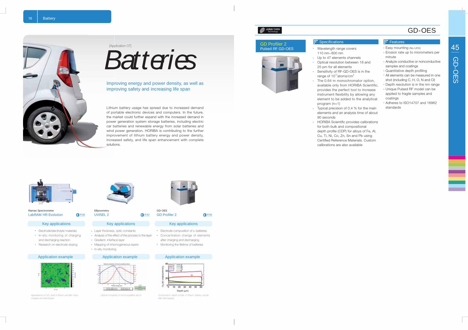
BatteriesGD Profi ler 2Pulsed RF GD-OES Easy mounting (No UHV)
Erosion rate up to micrometers per minuteAnalyze conductive or nonconductive samples and coatingsQuantitative depth profi lingAll elements can be measured in one shot (including C, H, O, N and Cl)Depth resolution is in the nm rangeUnique Pulsed RF model can be applied to fragile samples and coatingsAdheres to ISO14707 and 16962 standards
Wavelength range covers110 nm~800 nmUp to 47 elements channelsOptical resolution between 18 and 25 pm for all elementsSensitivity of RF-GD-OES is in the range of 1017atoms/cm2
The 0.64 m monochromator option, available only from HORIBA Scientific, provides the perfect tool to increase instrument flexibility by allowing any element to be added to the analytical program (n+1)Typical precision of 0.4 % for the main elements and an analysis time of about 90 secondsHORIBA Scientifi c provides calibrations for both bulk and compositional depth profi le (CDP) for alloys of Fe, Al, Cu, Ti, Ni, Co, Zn, Sn and Pb using Certifi ed Reference Materials. Custom calibrations are also available
FeaturesSpecifi cations
GD-OES
45
GD
-OE
S
GD Result SIMS Result
Thin fi lmsPowders
SemiconductorsMetallic alloys
Surface treatmentsCoated steel
Oxidation/Corrosion researchPolymer coatings
PVD/CVD coatingsCeramic/Glass
GD-OES
GD
-OE
S
44 Principle
Key Applications
Working Principle
RF-GD-OES systems are powerful tools to analyze material surface and interface elements. GD-OES combines a glow discharge powered by a radio frequency (RF) source with an optical emission spectrometer. Surface atoms of a sample are sputtered and eroded by Ar ions, layer by layer. The extracted atoms are excited by collisions in the plasma and emit some light. The emission light is detected by HDD through a polychromator (HDD: High Dynamic Range Detector).
Polychromater
Spectrometer Source
Sample
HJY Grating
Rowland circleHigh Dynamic Detector
Primary slit
Lens
Secondary slit
RF Glow Discharge Source
Sample
Cooling
Arwindow
Vacuum
vacuum
Anode
Hard disk analysis
A zoom of the near-surface region above (left) reveals the lubricant layer, diamond-like carbon protective layer, and the cobalt-chromium magnetic alloy and chromium layers, each layer approximately 20-30 nm thick, which were successively deposited over the disks. Sampling time of the near-surface region was 0.01 seconds. The image in (b) is a high magnifi cation view of the area in the red box at the top of (a) above.
Hard coating analysis
The above depth profi le shows the analysis of 25 layers of AIN/TIN (20 nm each) deposited on SI.
Comparison of the GD-OES and Secondary Ion Mass Spectrometry (SIMS)(Thin barrier anodic oxidation of aluminum)
A comparison of the GD-OES analysis and that of secondary ion mass spectrometry (SIMS) was made for this sample. The distribution of chromium in the fi lm compares well between the two techniques, however, the time of analysis was quite different. In GD-OES the time to reach the metal/oxide interface was 9 seconds, as compared to 60 minutes to reach this interface with SIMS.
Distance from oxide surface ( nm )
Cr
4.0
2.0
00 50
7nm
Inte
nsity
(a.u
.)
Distance from oxide surface ( nm )A film after anodizing in a sodium chromate solution
EMIA-920V2C/S/O/N/H Analyzer
XGT-5200X-Ray Fluorescence Analyzer
P.50 P.55 P.53
Evaluation of the effect on particle size distribution with different size ball-milling
Optical image, elements image and spectrum of separator of Li-ion battery
Lithium ion rechargeable batteries are one of the most popular types of rechargeable battery for portable electronics, like mobile phones and laptop computers.Carbon affects the lifetime of electrodes, so its concentration should be measured during the manufacturing process to confi rm that it's kept low.
LA-960Particle Analyzer Analyzer
Examples of HORIBA Scientifi c solutions
17Battery
Active Materials
Electrodes
Anodes
PVDF-based
SBR system
Positive electrode: AINegativeelectrode: CuPolyolefi n, etc.
Binders
Separator
Collecting foil
Causes of degradation HORIBA analysis instrument
Electrodes Anode
Key applications
Application example Application example Application example
Key applications Key applications
Particle size distribution of positive
electrode material
Particle size distribution of negative
electrode material
Foreign materials in separator
Metal particles inspection
Elements analysis in metal material
Elements analysis in inorganics
Crystallinity and crystal structural change based on Li-ion insertion and removalAtomization-based reactivity infl uence
Oxygen evolution in high-temperature environmentsElution of Mn ions (Mn system)Li Stoichiometry anomaly Contamination, moisture absorption and oxidation toward active materialsUneven distribution and gaps in active materialCrystallinity Evaluation of carbons based on Li-ion insertion and removalAtomization-based reactivity infl uence
Reactivity decrease due to SEI formationContamination, moisture absorption and oxidation toward active materialsUneven distribution and gaps in active material
Oxidation of cells based on residual NMPSeparation and uneven distribution due to binding failure
pH control of negative electrode slurry adjustment process and part ic le s ize managementSeparation and uneven distribution due to binding failure
Surface oxidation and corrosion
Separator damage from shattering and burrs
Surface oxidation and corrosion
Raman Spectroscopy
Particle size distribution analyzer, SEM-EDXOxygen analysis analyzer
ICP-OESGD-OESFluorescent X-Rays, carbon and sulphur analysis analyzerFluorescent X-rays, SEM-EDXRaman SpectroscopySEM-CLParticle size distribution measuring apparatus, SEM-EDXGD-OESFluorescent X-Rays, carbon and sulphur analysis analyzerFluorescent X-Rays, SEM-EDX
pH, Particle size distribution analyzer
SEM-EDX
GD-OES, SEM-EDX
GD-OES, SEM-EDX
Fluorescent X-Rays, SEM-EDX
Residual gas analyzerSEM-EDX
Separator (foreign matter)
Coating
Binders and conductive assistants
Binders
SEI
Anode active material (Crystallinity)
Cathode active materials (Composition)
Precipitated phase (Oxides)
LabRAM HR EvolutionRaman Spectrometer
GD Profi ler 2GD-OES
P.30 P.45UVISEL 2Ellipsometry
P.42
18 Energy / Solar cell
[Application 08]
Solar batteries are utilized as renewable energy, and HORIBA's analysis and control systems demonstrate superior performance. We are contributing to the high effi ciency and quality improvement of solar batteries in the semiconductor and FPD processes.
Improving the analysis, evaluation, cell lifespan and durability of solar cell materials, from semiconductor materials to dye-sensitization
EnergySolar Cells
Key applications
Application example Application example Application example
Key applications Key applications
Calculation of Si crystalline ratio Optical constants of microcrystalline silicon Compositional depth profi le of a solar cell
Si solar cells crystallinity ratio
measurement
Crystal size analysis of Si solar cells
Structure analysis of thin fi lm solar cells
Charge and discharge analysis
Deposition process of PV
Interlamination diffusion of PV
Surface and composition of PV
Fast depth profi ling
Layer thickness, optic constants
Analysis of the effect of the process on
the layer
Gradient, interface layer
Mapping of inhomogeneous layers
In-situ monitoring
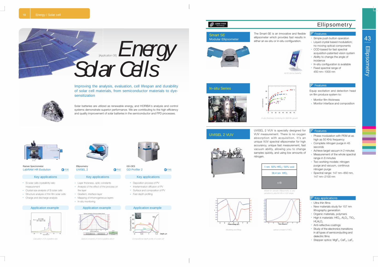
AUTO Soft & DeltaPsi
Smart SEModular Ellipsometer
GaN
TH
ICKN
ESS
(Å)
0
20
40
60
0 10 20 30 40 50 60 70
200 C
600 C
450 C
150 C 70 C
In-situ Series
UVISEL 2 VUV
Ellipsometry
Ellip
sometry
43Features
Features
Features
Key applications
The Smart-SE is an innovative and fl exible ellipsometer which provides fast results in either an ex-situ or in-situ confi guration.
Simple push button operationLiquid crystal based modulation; no moving optical componentsCCD-based for fast spectralacquisition-patented vision systemAbility to change the angle of incidenceIn-situ confi guration is availableFixed spectral range of450 nm~1000 nm
Monitor fi lm thicknessMonitor interface and composition
Equip excitation and detection head on fi lm produce system to:
In-situ thickness monitoring for GaN fi lm growth
UVISEL 2 VUV is specially designed for VUV measurement. There is no oxygen absorpt ion wi th acquis i t ion. I t ’s an unique VUV spectral ellipsometer for high accurancy, unique fast measurement, fast vacuum ability, allowing you to change samples quickly, and using low amounts of nitrogen.
1 nm 50% HfO2 / 50% void
c-Si
36.4 nm HfO2
Model for sample; Ellipsometry is very sensitive to ultra thin fi lm in VUV range.
Phase modulation with PEM at as high as 50 KHz frequencyComplete nitrogen purge in 45 secondsAchieve target vacuum in 2 minutesMeasurement of the whole spectral range in 8 minutesTwo working models: nitrogen purge and vacuum, continous nitrogen purgeSpectral range: 147 nm~850 nm, 147 nm~2100 nm
optical constant of HfO2 Modeling and fi tting
Ultra thin fi lmsNew materials study for 157 nm lithography generationOrganic materials, polymersHigh k materials: HfO2, Al2O3, TiO2, HfxAlyOz
Anti-refl ective coatingsStudy of the electronics transitions in all types of semiconducting and dielectric fi lmsStepper optics: MgF2, CaF2, LaF3
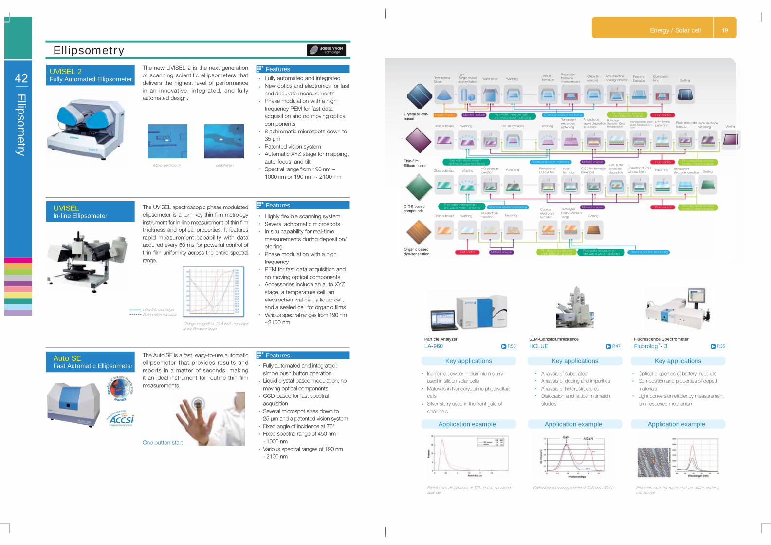
UVISEL 2Fully Automated Ellipsometer
UVISELIn-line Ellipsometer
Auto SEFast Automatic Ellipsometer
Ellipsometry
Ellip
sometry
42The new UVISEL 2 is the next generation of scanning scientific ellipsometers that delivers the highest level of performance in an innovative, integrated, and fully automated design.
Micro-electronics Graphene
Fully automated and integratedNew optics and electronics for fast and accurate measurementsPhase modulation with a high frequency PEM for fast data acquisition and no moving optical components8 achromatic microspots down to 35 μmPatented vision system Automatic XYZ stage for mapping, auto-focus, and tiltSpectral range from 190 nm ~ 1000 nm or 190 nm ~ 2100 nm
The UVISEL spectroscopic phase modulated ellipsometer is a turn-key thin fi lm metrology instrument for in-line measurement of thin fi lm thickness and optical properties. It features rapid measurement capability with data acquired every 50 ms for powerful control of thin fi lm uniformity across the entire spectral range.
Ultra-thin monolayerFused silica substrate
Change in signal for 10 A thick monolayer at the Brewster angle
Highly fl exible scanning systemSeveral achromatic microspotsIn situ capability for real-time measurements during deposition/etchingPhase modulation with a high frequency PEM for fast data acquisition and no moving optical componentsAccessories include an auto XYZ stage, a temperature cell, an electrochemical cell, a liquid cell, and a sealed cell for organic fi lmsVarious spectral ranges from 190 nm~2100 nm
Features
Features
FeaturesThe Auto SE is a fast, easy-to-use automatic ellipsometer that provides results and reports in a matter of seconds, making it an ideal instrument for routine thin film measurements.
One button start
Fully automated and integrated; simple push button operationLiquid crystal-based modulation; no moving optical componentsCCD-based for fast spectral acquisitionSeveral microspot sizes down to 25 μm and a patented vision systemFixed angle of incidence at 70°Fixed spectral range of 450 nm~1000 nmVarious spectral ranges of 190 nm~2100 nm
P.50LA-960Particle Analyzer
P.47HCLUESEM-Cathodoluminescence
Fluorolog®- 3Fluorescence Spectrometer
P.35
19Energy / Solar cell
Key applications
Application example Application example Application example
Key applications Key applications
Inorganic powder in aluminium slurry
used in silicon solar cells
Materials in Nanocrystalline photovoltaic
cells
Silver slurry used in the front gate of
solar cells
Analysis of substrates
Analysis of doping and impurities
Analysis of heterostructures
Dislocation and lattice mismatch
studies
Optical properties of battery materials
Composition and properties of doped
materials
Light conversion effi ciency measurement
luminescence mechanism
Particle size distributions of TiO2 in dye-sensitized solar cell
Emission spectra measured on wafer under a microscope
Film deposition process control/Thin fi lm analysis
Film deposition process control/Thin fi lm analysis
Film deposition process control/Thin fi lm analysis
Film deposition process control/Thin fi lm analysis
XploRA NanoAFM-Raman
Auto SEEllipsometry
Fluorolog®- 3Fluorescence Spectrometer
P.30 P.42 P.35
Colorimetric analysis of light-emitting devicesThiol Self Assembled Monolayer AFM (left) and Raman (right) mapping
Optical properties of AIN and the overlayer
20 Organic Electronics
[Application 09]
As a cost-effective and good-performance technology, organic electronics, such as OLED, OEL, TFT and OPV are making a profound influence on the information industry, in fact, on whole economy and society. HORIBA Scientifi c provides excellent solutions for the study and characterization of organic electronic materials.
Application example Application example Application example
Key applications Key applications
Crystal type analysis
Doping/defect research
Stress distribution
Identify pollutants
Photo- and electroluminescence
Layer thickness, optical constants
Anisotropy, crystalinity
Alloy ratio
Energy gap
Photoresistance, polymers
Optical properties of luminescence materials
Absolute quantum effi ciency measurement
Colorimetric analysis
Life-time analysis
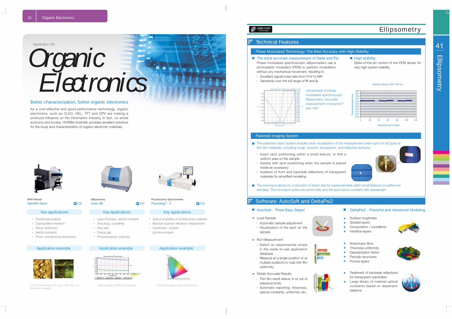
Phase modulated spectroscopic ellipsometers use a photoelastic modulator (PEM) to perform modulation without any mechanical movement, resulting in:
Uniqueness of phase modulated spectroscopicEllipsometry: Accurate measurement of around 0° and 180°
State-of-the-art control of the PEM allows for very high system stability
Measurement number
Stability (3days) -NIST 100 nm
0 20 40 60 80 100 120
980979978977976975974973972971970
Thic
knes
s(A
ngst
rom
s)
Excellent signal/noise ratio from FUV to NIRSensitivity over the full range of Ψ and Δ
Ellipsometry
Ellip
sometry
41Technical Features
Software: AutoSoft and DeltaPsi2
Phase Modulated Technology: The Best Accuracy with High Stability
Patented Imaging System
The most accurate measurement of Delta and Psi High stability
AutoSoft - Three Easy Steps! DeltaPsi2 - Powerful and Advanced Modeling
The patented vision system enables clear visualization of the measurement beam spot on all types of thin fi lm materials, including rough, smooth, transparent, and refl ective surfaces:
Exact spot positioning within a small feature, or find a uniform area on the sampleAssists with spot positioning when the sample is placed inside an accessoryIsolation of front and backside reflections of transparent materials for simplifi ed modeling
The microspot allows for a reduction in beam size for measurements within small features on patterned samples. The microspot optics are achromatic and the spot size is constant with wavelength.
Treatment of backside refl ections for transparent substratesLarge library of material optical constants based on dispersion relations
Anisotropic fi lmsThickness uniformityDepolarization factorPeriodic structuresPorous layers
Obtain Accurate Results
Run Measurement
Automatic sample adjustmentVisualization of the spot on the sample
Thin fi lm result status: in or out of tolerance limitsAutomatic reporting: thickness, optical constants, uniformity, etc.
Select an experimental recipe in the ready-to-use application databaseMeasure at a single position or at multiple positions to map thin fi lm uniformity
Film thickness from a few Angstroms to tens of micronsOptical constants (n,k)Material properties: compound alloy composition, porosity, crystallinity, anisotropy, optical bandgap
Ellipsometry
Ellip
sometry
40 Principle
Key Applications
Spectroscopic ellipsometry is a non-destructive and non-contact optical technique which is based on the change in the polarization state of light as it is refl ected obliquely from a thin fi lm sample. Ellipsometry utilizes a model-based approach to determine thin fi lm thickness, optical properties, and more.
Measurement Modeling Results
Light source
Polarizer
Detector
Analyzer
PEM
Sample
Optical constants
Film thickness
Information Obtained from EllipsometryNon-destructive and non-contactVery sensitive, especially to ultra-thin fi lms (<10 nm)In-situ real-time monitoring of thin film deposition or etching by rapid kinetic measurementsNo sample preparation
In the long annals of human history, countless works of art have been created by our ancestors, such as beautiful jade sculptures, paintings, ceramics, textiles, glass, and more. Investigating the minerals, pigments, enamel, fi bers and lacquer helps protect these priceless relics and helps us understand human culture. HORIBA Scientific can help analyze the cultural relics and artifacts, quickly and non-destructively.
Precious cultural relics and art need non-destructive and fast analysis
Archeometry
Key applications
Application example Application example Application example
Key applications Key applications
Paint/pigment analysis
Art and antiques restoration
Metals and alloys
Paints, inks and pigments
Gemstones
Corrosion products
Internal analysis of authenticity
Pigment analysis and authentication
Glaze color analysis of ceramic
Composition and aging of silk
Corrosion analysis of metalware
Mineral and fl uid inclusion
Red fresco pigment analysis of Pompeii Micro-XRF imaging of an ancient Nepalese manuscript
Fluorescence lifetime image overlaid on a camera image of a patterned area of a banknote.
About Us
Key Applications
Gold coated master gratings
VUV custom gratings
Custom gratings for astronomy and space fl ight
Multi-layer dielectric gratings
Products
Manufacturing
22
Scientifi c G
ratings
Scientifi c Gratings
Founded in 1819, HORIBA Scientifi c, formerly Jobin Yvon, has been leading the industry in optics for spectroscopy for over 190 years. Our leadership in optics has been demonstrated by the continuing development of both ruled and holographic grating technology, including the invention of aberration-corrected holographic gratings and ion-etched blazed holographic gratings.
We are partnering with leading researchers, worldwide, to explore new technology areas and to provide higher specifi cations.
HORIBA’s scientifi c/custom diffraction gratings are found in cutting-edge scientifi c applications including ultrafast and high-energy lasers, space fl ight instruments, astronomy, and synchrotron spectrometers.
Pulse compression for high power lasers360 mm x 565 mm1200 gr/mm, 1480 gr/mm, 1740 gr/mm800 nm, 1064 nm, 1550 nm>90 %
Application:
Maximum size: Groove density:
Wavelength:Effi ciency:
Application:
Application:
Provide custom design gratings for astronomy and space experiments
Application:
Maximum size: Groove density: Wavelength: Effi ciency:
Pulse compression for high power lasers430 mm x 470 mm1740 gr/mm1053 nm92-95 %
Provide custom design based on specific requirements:
Groove density: up to 5600 gr/mmRefl ection or transmission grating designLow stray light and high effi ciencySpectral range from EUV to Mid-IRSpace qualifi ed - TRL9
Astronomy and space experiments
The SPRi-CFM is an automatic printer that uses flow deposition for printing biomolecules. Samples are cycled over the surface and captured from solution, leading to higher biomolecule density, better spot uniformity and improved assay sensitivity.
SPRi-CFM printing of a protein from a low to a high concentration in quadruplicate
Surface Plasmon Resonance imaging (SPRi)
Surface P
lasmon R
esonance imaging (S
PR
i)
NEWNEW
Screenshot of the SPRi-View software
EzPlex is the ideal solution for label-free bio-assays. EzPlex combines the power of multiplexing (measuring multiple interactions
simultaneously) and the sensitivity of Surface Plasmon Resonance, resulting in high-resolution kinetic profi les.
Multiplex detection of several hundred interactionsLabel-free interaction detection of proteins, peptides, DNA, RNA, cells, small molecules Real-time monitoringDetermination of kinetic parameters and affi nityDifference image display gives a direct view of reactions as the experiment unfoldsTemperature controlSample recovery functionSample recyclingUser-friendly software
Features
Features
Features
Features
OpenPlex is a flexible Surface Plasmon Resonance imaging system. It is a robust and compact system designed for simplicity and versatility. Its open format, dedicated sensor chips and manual operation enables many types of experiments.
With the courtesy of Dr Marinella Sandros from JSNN, USA
Label-free interaction analysis Real-time monitoring of kinetic curves Determination of affi nity/kinetic parameters Multiplexed imaging (up to 400 spots)
Different fl ow cell confi gurationsMinimal maintenance
Easy to usePrints onto SPRi-Biochips, SPRi-Slides™ and standard glass slidesCapture and deposition ofmolecules from complex samplesNo cross-contaminationIncreased spotting reproducibility and uniformityEnhanced assay sensitivity
Easy to operate with fast system start up and simple installationRobust, compact and portable designOperates with uniquely optimized composite printing pinsIntegrated micro-array image processing and data analysis toolsPrints onto different supports
Accessories
SPRi-Arrayer makes it easy to print biological micro-arrays on a biochip surface to suit your experiment, whether it’s gold, glass or membrane substrate, thus adding versatility to your experiment or assay.
CRP_Specifi c Aptamer Control
38
Surface Plasmon Resonance imaging (SPRi)
Surface P
lasmon R
esonance imaging (S
PR
i)
Principle
Key Applications
PrincipleSurface Plasmon Resonance imaging (SPRi) is an optical detection process that occurs when a polarized light hits a prism covered by a thin (gold) metal layer. Under certain conditions (wavelength, polarization and incidence angle), free electrons at the surface of the biochip absorb incident light photons and convert them into surface plasmon waves. A dip in refl ectivity of the light is seen under these SPR conditions.
The SPR imaging technology takes SPR analysis a step further for biomolecular interaction analysis. It is a sensitive label-free method of visualizing the entire biochip via a video CCD camera. This design enables the biochips to be prepared in an array format with each active site (spot) providing SPR information simultaneously and in real-time.
Exit port Injection port
Prism
Light source
Detector
Features
SPRi Combined with MALDI Mass Spectrometry (MS)
Optimization and comparison parameters
Test for different concentrations, buffers or pH on the same sensor chip, and optimize the experimental conditions of your interaction models. Use as many replicate spots as you wish to be more confi dent in the results.
Spot up to several hundred different molecules on the biochipMonitor the biomolecular interactions of each spot simultaneously in real timeHave access to quantitative and qualitative information (kinetic curve and
difference image) simultaneously.
DNA / RNA
DNA / DNA
Protein / carbohydrate
DNA / Protein
Antibody / Bacteria Peptide / Protein
Protein / Protein
Combination of SPRi and MALDI-MS Analysis- Analysis on the same biochipDirect MS analysis on SPRi microarray chip- No recovery of the sampleMultiplexed analysis of many spatially resolved samples- Save time and consumables
Instant affi nity profi ling
By using a single-injection step the affinity of analytes binding to different ligands can be determined using only one analyte concentration injection (no regeneration step required) – saving you time and samples.
Small molecule detection
The revolutionary optical and fluidics units obtain unsurpassed performance for high-sensitivity measurements. The instrument is compatible with the use of solvents, such as DMSO.
Rank and screen your molecules
Multiplexing helps you to rank and screen molecules such as antibodies or aptamers according to affinity or kinetic rates, easily and rapidly.
TGM/TGS SeriesSpectrometer
PGM/PGS SeriesSpectrometer
VHR 640/1000Spectrometer
UVL Series Spectrometer
23
VUV Systems
VU
V S
ystems
About Us
Key Applications
Applications
Applications
Applications
Applications
HORIBA Scientifi c supplies vacuum spectroscopy components covering 1 nm to NIR in vacuum environment, such as light sources, sample chambers, monochromators, detectors, accessories, and more. Our instruments are designed using state-of-the-art spherical, plane, toroidal or cylindrical optics, gratings and mirrors with micro mechanic movements in High and Ultra High Vacuum chambers. We offer our technical expertise in customizing optical spectroscopy systems with high throughput, low aberration, and high resolution optimized for your spectral ranges and applications.
Tunable VUV light sources, VUV fl uorescence excitation, transmission/refl ection/absorption, XPS, plasma spectroscopy, VUV photoluminescence, VUV laser, high-order harmonic generation.HORIBA Scientifi c also offers customized VUV optical spectroscopy systems, including full synchrotron beamlines.
Optical design: single gratingsGrating: spherical type IV gratingSpectral range: 50 nm - 600 nmFocal length: 200 mm and 300 mmSpectral resolution: better than 0.1 nmVacuum: 10-5 mbar/10-9 mbarCompatible with single channel detectors & non-vacuum systems
Optical design: single gratingGrating: aberration-corrected toroidal master/replica gratingSpectral range: 1 nm - 400 nmFocal length: 300 mm - 4500 mmSpectral resolution: up to 0.01 nmVacuum: 10-6 mbar/10-9 mbarCompatible with single/multi-channel detectors & non-vacuum systems
Optical design: mirror + gratingGrating: aberration-corrected plane master/replica gratingMirror: toroidal mirrorSpectral range: 1 nm - 125 nmFocal length: 200 mm - 1000 mmSpectral resolution: up to 0.008 nmVacuum: 10-8 mbar/10-9 mbarCompatible with single/multi-channel detectors & non-vacuum systems
Optical design: Czemy-TurnerGrating: plane gratingMirror: toroidal mirrorSpectral range: 100 nm - 15 μmFocal length: 640 mm/1000 mmSpectral resolution: up to 0.005 nmVacuum: 10-5 mbarCompatible with single/multi-channel detectors
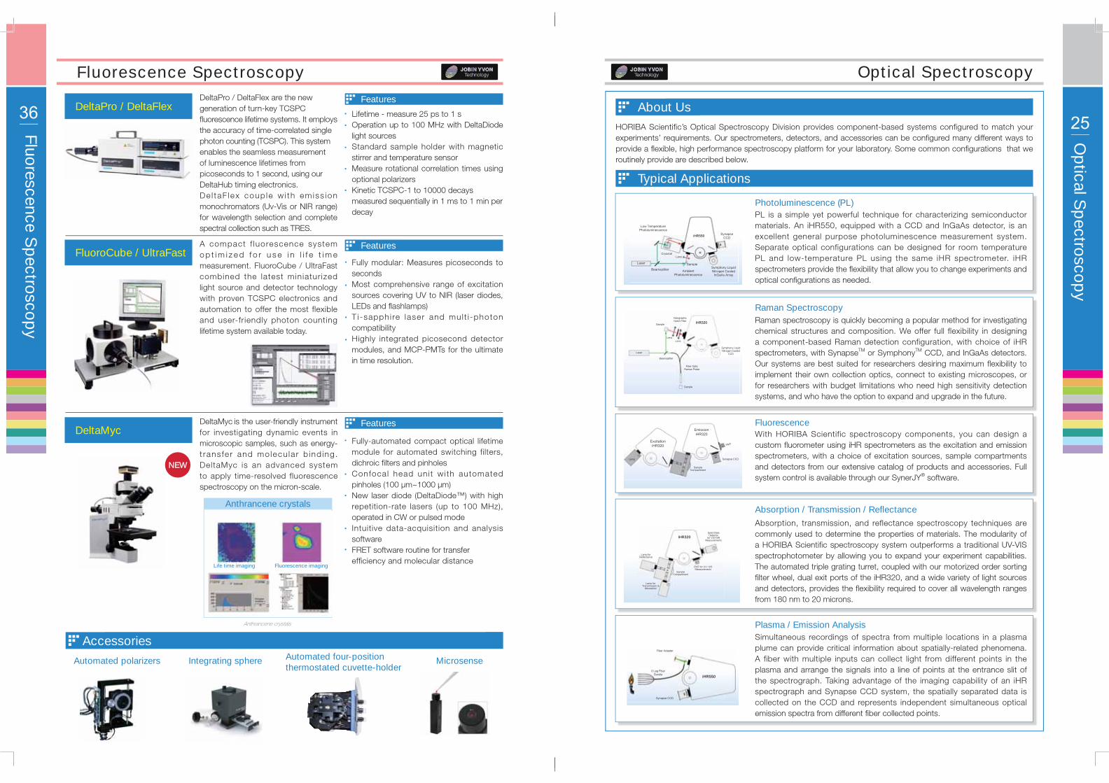
HORIBA Scientifi c, formerly Jobin Yvon, continues transferring its valuable knowledge obtained in the production of high-end scientifi c gratings and instruments to volume production of industry gratings and spectrometers. Thanks to its strong capability in research and development in optical spectroscopy design and production, HORIBA Scientifi c continuously cooperates with instrument manufacturers to help them update their own products, increasing their added value and developing their next generation of instrumentation.
HORIBA’s OEM products are widely used in many applications, including biomed, light source measurement, HPLC, water and gas analysis, telecom, ICP, Raman, fl uorescence, lasers, etc.
According to customers’ requirements and applications, HORIBA Scientific can provide gratings, spectrometer modules and complete solutions. Our experts in optical spectroscopy will share their experience, work with customized specifi cations, and help fi nalize products’ designs, all at a reasonable price.
As a major OEM provider in optical spectroscopy, HORIBA Scientifi c observes a strict confi dentiality policy and is fully compliant with the industry standards, including NDA, traceability, and quality control. Our OEM division pursues a long term win-win cooperation with customers and manufacturers, alike.
Type I holographic concave grating
Diffraction gratings
Type IV aberration-corrected monochromator grating
Customized spectrometers
Type IV aberration-corrected fl at fi eld grating
Customized optical spectroscopy solutions
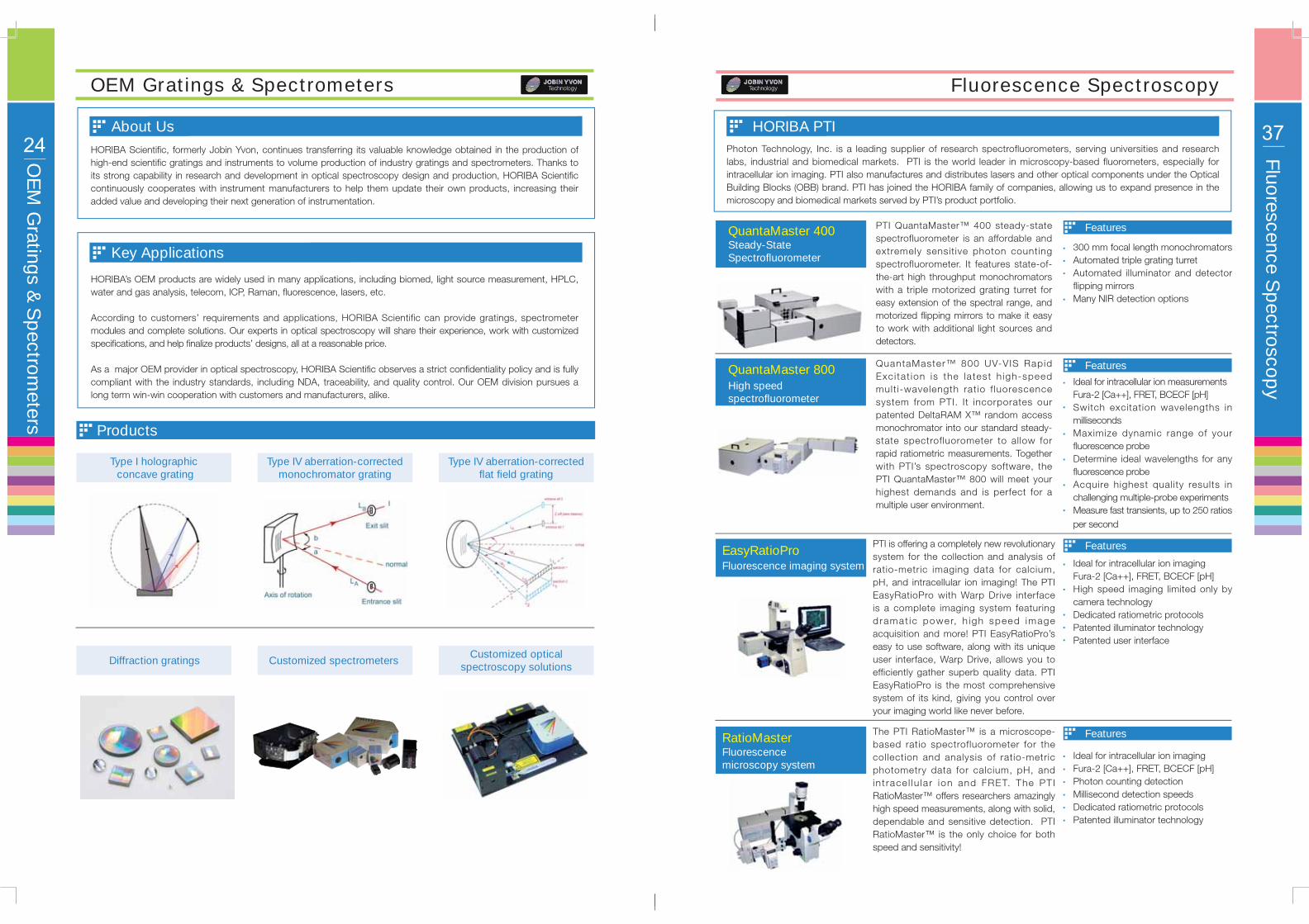
37
QuantaMaster 800
EasyRatioPro
RatioMaster
Fluorescence Spectroscopy
Fluorescence Sp
ectroscopy
300 mm focal length monochromatorsAutomated triple grating turretAutomated illuminator and detector fl ipping mirrorsMany NIR detection options
Ideal for intracellular ion imagingFura-2 [Ca++], FRET, BCECF [pH]High speed imaging limited only by camera technologyDedicated ratiometric protocolsPatented illuminator technologyPatented user interface
Ideal for intracellular ion imagingFura-2 [Ca++], FRET, BCECF [pH]Photon counting detectionMillisecond detection speedsDedicated ratiometric protocolsPatented illuminator technology
Ideal for intracellular ion measurementsFura-2 [Ca++], FRET, BCECF [pH]Switch excitation wavelengths in millisecondsMaximize dynamic range of your fl uorescence probeDetermine ideal wavelengths for any fl uorescence probeAcquire highest quality results in challenging multiple-probe experimentsMeasure fast transients, up to 250 ratios per second
HORIBA PTI Photon Technology, Inc. is a leading supplier of research spectrofluorometers, serving universities and research labs, industrial and biomedical markets. PTI is the world leader in microscopy-based fluorometers, especially for intracellular ion imaging. PTI also manufactures and distributes lasers and other optical components under the Optical Building Blocks (OBB) brand. PTI has joined the HORIBA family of companies, allowing us to expand presence in the microscopy and biomedical markets served by PTI’s product portfolio.
QuantaMaster 400Steady-State Spectrofl uorometer
PTI QuantaMaster™ 400 steady-state spectrofluorometer is an affordable and extremely sensit ive photon counting spectrofluorometer. It features state-of-the-art high throughput monochromators with a triple motorized grating turret for easy extension of the spectral range, and motorized flipping mirrors to make it easy to work with additional light sources and detectors.
QuantaMaster™ 800 UV-VIS Rapid Exci tat ion is the latest h igh-speed mult i-wavelength rat io f luorescence system from PTI. It incorporates our patented DeltaRAM X™ random access monochromator into our standard steady- state spectrofluorometer to allow for rapid ratiometric measurements. Together with PTI’s spectroscopy software, the PTI QuantaMaster™ 800 will meet your highest demands and is perfect for a multiple user environment.
PTI is offering a completely new revolutionary system for the collection and analysis of ratio-metric imaging data for calcium, pH, and intracellular ion imaging! The PTI EasyRatioPro with Warp Drive interface is a complete imaging system featuring dramat ic power, h igh speed image acquisition and more! PTI EasyRatioPro’s easy to use software, along with its unique user interface, Warp Drive, allows you to efficiently gather superb quality data. PTI EasyRatioPro is the most comprehensive system of its kind, giving you control over your imaging world like never before.
The PTI RatioMaster™ is a microscope-based ratio spectrofluorometer for the collection and analysis of ratio-metric photometry data for calcium, pH, and in t race l lu la r ion and FRET. The PTI RatioMaster™ offers researchers amazingly high speed measurements, along with solid, dependable and sensitive detection. PTI RatioMaster™ is the only choice for both speed and sensitivity!
Features
Features
Features
Features
High speed spectrofl uorometer
Fluorescence imaging system
Fluorescence microscopy system
36
FluoroCube / UltraFast
DeltaMyc
DeltaPro / DeltaFlex
Fluorescence Spectroscopy
Fluorescence Sp
ectroscopy
NEWNEW
Features
Features
Features
DeltaPro / DeltaFlex are the new generation of turn-key TCSPC fl uorescence lifetime systems. It employs the accuracy of time-correlated single photon counting (TCSPC). This system enables the seamless measurement of luminescence lifetimes from picoseconds to 1 second, using our DeltaHub timing electronics. De l taF lex coup le w i th emiss ion monochromators (Uv-Vis or NIR range)for wavelength selection and complete spectral collection such as TRES.
Lifetime - measure 25 ps to 1 sOperation up to 100 MHz with DeltaDiode light sourcesStandard sample holder with magnetic stirrer and temperature sensor Measure rotational correlation times using optional polarizers Kinetic TCSPC-1 to 10000 decaysmeasured sequentially in 1 ms to 1 min per decay
A compact f luorescence system o p t i m i z e d f o r u s e i n l i f e t i m e measurement. FluoroCube / UltraFast combined the latest miniatur ized light source and detector technology with proven TCSPC electronics and automation to offer the most flexible and user-friendly photon counting lifetime system available today.
Fully modular: Measures picoseconds to secondsMost comprehensive range of excitation sources covering UV to NIR (laser diodes, LEDs and fl ashlamps)T i -sapphi re laser and mul t i -photon compatibilityHighly integrated picosecond detector modules, and MCP-PMTs for the ultimate in time resolution.
Anthrancene crystals
Fluorescence imagingLife time imaging
Anthrancene crystals
DeltaMyc is the user-friendly instrument for investigating dynamic events in microscopic samples, such as energy-t ransfer and molecu lar b ind ing. DeltaMyc is an advanced system to apply time-resolved fluorescence spectroscopy on the micron-scale.
Accessories
Fully-automated compact optical lifetime module for automated switching filters, dichroic fi lters and pinholesConfocal head uni t with automated pinholes (100 μm~1000 μm) New laser diode (DeltaDiode™) with high repetition-rate lasers (up to 100 MHz), operated in CW or pulsed modeIntuitive data-acquisition and analysis software FRET software routine for transfer effi ciency and molecular distance
HORIBA Scientific’s Optical Spectroscopy Division provides component-based systems configured to match your experiments’ requirements. Our spectrometers, detectors, and accessories can be confi gured many different ways to provide a fl exible, high performance spectroscopy platform for your laboratory. Some common confi gurations that we routinely provide are described below.
PL is a simple yet powerful technique for characterizing semiconductor materials. An iHR550, equipped with a CCD and InGaAs detector, is an excellent general purpose photoluminescence measurement system. Separate optical configurations can be designed for room temperature PL and low-temperature PL using the same iHR spectrometer. iHR spectrometers provide the fl exibility that allow you to change experiments and optical confi gurations as needed.
Raman spectroscopy is quickly becoming a popular method for investigating chemical structures and composition. We offer full flexibility in designing a component-based Raman detection configuration, with choice of iHR spectrometers, with SynapseTM or SymphonyTM CCD, and InGaAs detectors. Our systems are best suited for researchers desiring maximum fl exibility to implement their own collection optics, connect to existing microscopes, or for researchers with budget limitations who need high sensitivity detection systems, and who have the option to expand and upgrade in the future.
With HORIBA Scientific spectroscopy components, you can design a custom fl uorometer using iHR spectrometers as the excitation and emission spectrometers, with a choice of excitation sources, sample compartments and detectors from our extensive catalog of products and accessories. Full system control is available through our SynerJY® software.
Absorption, transmission, and reflectance spectroscopy techniques are commonly used to determine the properties of materials. The modularity of a HORIBA Scientifi c spectroscopy system outperforms a traditional UV-VIS spectrophotometer by allowing you to expand your experiment capabilities. The automated triple grating turret, coupled with our motorized order sorting fi lter wheel, dual exit ports of the iHR320, and a wide variety of light sources and detectors, provides the fl exibility required to cover all wavelength ranges from 180 nm to 20 microns.
Simultaneous recordings of spectra from multiple locations in a plasma plume can provide critical information about spatially-related phenomena. A fiber with multiple inputs can collect light from different points in the plasma and arrange the signals into a line of points at the entrance slit of the spectrograph. Taking advantage of the imaging capability of an iHR spectrograph and Synapse CCD system, the spatially separated data is collected on the CCD and represents independent simultaneous optical emission spectra from different fi ber collected points.
Photoluminescence (PL)
Raman Spectroscopy
Fluorescence
Absorption / Transmission / Refl ectance
Plasma / Emission Analysis
26
Op
tical Sp
ectroscopy
Fully integrated, high throughputWide spectral range, simple to useVersatile and compatible with multiple lasersDown-looking or side-looking objective availableCost effective microspectrometer
Versatility, high performance in a small packageMicroHR compatible with CCD/IGA array, PMT or solid state detectorIdeal for at-line diagnostics, fi eld measurement, etc.
Superior imaging performancePatented on-axis grating drive Asymmetric layout eliminates re-diffracted lightChoice of 2 entrance and 2 exit portsIdeal for photoluminescence, Raman, fl uorescence, etc
MicOS
MicroHRSmall spectrometer
iHR320 / 550Imaging spectrometer
FHR640 / FHR1000High resolution spectrometer High spectral resolution
High scanning speed, reduces overall experiment timeRobust cast body for optimal performance without wavelength shifts and signal loss
Very easy to operateLow cost time-resolved fi lter-based fl uorometerIdeal for undergraduate teaching labsIdeal as a lifetime companion to any spectrofl uorometerComprehensive decay analysis software, MEM distribution analysis
EasyLife X / EasyLife LLow cost fl uorescencelifetime fi lter fl uorometer
Focal length: 640 mm / 1000 mmGrating size (mm): 80 x 110 or 110 x 110Aperture ratio: 5.4 / 9PMT resolution: 0.016 nm / 0.01 nmDispersion (nm/mm): 1.2 / 0.8Scan speed: 300 nm/s
Light source: 150 W Xenon lampSesitivity (SNR)- 6000:1 FSD method*- 16000:1 RMS methodAll-refl ective opticsTime-correlated single-photon counting (TCSPC) accessory for lifetime determinations Phosphorimeter accessory for long-lived luminescence determinations
Light source: 450W Xenon lampSpectra range: 185 nm~14 μmSensitivity (SNR)- 12000 > 10000:1 FSD method*- 30000 > 20000:1 RMS methodAll-refl ective opticsTotally computer-controlledInterchange wide range of computer-controlled accessories: spectrometers, detectors, sources, and more
Fluorolog Extreme
Fluorolog®-3
NanoLog®
FluoroMax®-4/Plus (P/TCSPC)
Fluorescence Spectroscopy
Fluorescence Sp
ectroscopy
35Features
Features
Features
Features
NEWNEW
The Fluorolog®-3 is a unique, modular system which al lows the researcher to in terchange a versat i le range of accessories to correspond perfectly with the characteristics of a given sample. From analysis of steady-state or molecular dynamics to IR probes, the Fluorolog®-3 comes equipped with a wide range and limitless configuration of accessories to enhance the accuracy and speed of your application.
The F luoro log® Extreme seamless ly combines our fluorometers with the high intensity and broad wavelength range of the supercontinuum lasers. It is a very bright source that simultaneously puts out light at a very wide spectral range from just above 400 nm to over 2 μm. Because of their brightness and broad spectral range, they make excellent sources for steady-state and lifetime (ps to 10 s) measurements.
The FluoroMax® ser ies is a compact spectrofl uorometer, yet it employs photon-counting for the ultimate sensitivity in f luorescence investigations as well as features not found in most table-top fl uorescence-detection systems.
3-D matrix scan over a range of excitation wavelengths of a sample of petroleum
Select any excitation wavelength (400 nm~2 μm)More excitation power for weak fl uorescence signals, especially in the NIRAll-refl ective opticsComplete optical, mechanical and software integration
The NanoLog® series of spectrofl uorometers are specif ically designed for research in nanotechnology and the frontiers of nanomaterials. A complete spectrum can be scanned as fast in as a few milliseconds, and a full excitation-emission matrix scan can be taken in as little as seconds.
Emission-excitation scan of a mixture of single-walled carbon nanotubes
*Note: This method considers that noise is also infl uenced by factors like the quality of the optics and scattered light in the system.
Rapid excitation-emission matrices in secondsHigh sensitivity in near-IR with InGaAs arrayAll-refl ective opticsEases qualifi cation and quantifi cation of species and families of SWCNTs Resolve mixtures of quantum dots simultaneously Modular design to accommodate any experimental setup Compatible with a variety of detectors from UV to near-IR
Excitation:360nm
Inte
nsity
Emission Wavelength (nm)
Fluo
resc
ence
(a.u
.) 1.14
1.12
1.10
1.08
1.06
1.04
1.02
1.00
800
900
1000
1100
1200
1300
1400
1500
1600
Wavelength (nm)
Fluo
resc
ence
0450 500 550 600 650
700
Wavelength (nm)
600000
500000
400000
300000
200000
100000
Aqualog® / Dual-FL
Fluorescence Spectroscopy
Fluorescence Sp
ectroscopy
34 Principle
Fluorescence is luminescence that results when an electron of a molecule absorbs energy of a specifi c wavelength, and then falls back from a higher energy-level to its original level, releasing the energy as light.
HORIBA Scientifi c, the global leader in Fluorescence Spectroscopy instrumentation, offers the most extensive line of Fluorescence Steady-State, Fluorescence Lifetime, hybrid instruments and microscope-based solutions.
Characterization of new organic moleculesFluorescent probesReaction mechanisms and quantum dotsAnalysis of nanoparticles
Characterization ofsunscreensPigmentationcharacterizationSkin-aging studiesSkin, hair, and tooth fl uorescence
Dosage of chemical solutions
Key Applications
Biology/Life science
Cell mechanismsInteractions of proteinsSinglet-oxygen detectionMembrane mobilityIntracellular calcium fl ow
EmissionExcitation
Collagen
Derm
Skin
Tryptophan
Fluorescence of the skin, hair and teeth
Analysis of nanoparticles of erbium in YbPO4 with the Fluorolog®-3
Emission spectra of quantum dots
Emission spectra of a wafer using the Fluorolog®-3 coupled with a microscope (Diameter of the zone studied: 1 μm)
Aqualog® / Dual-FL combine the world’s only CCD-based benchtop spectrofl uorometer with a UV-VIS spectrophotometer. It is the only instrument to simultaneously measure both absorbance spectra and fl uorescence Excitation-Emission Matrices.
EEMs are acquired up to 100 times faster than with other instruments. Dedicated software automates traceable Quinine Sulfate Unit calibration and correction of inner-fi lter effects and Rayleigh and Raman scattering lines.
Features
The only true simultaneousabsorbance-fl uorescence system availableThe fastest acquisition speed of EEMs (s~min)Light source: 150 W Xenon lampSpectra range: 200 nm~800 nm(UV-NIR model, full-range calibration)
Ultra bright optical powerIdeal for solar illuminatorsIdeal for tunable monochromator illuminationChoice of lamps (75 W Xe,100 W Hg, 100 W TH, 150 W Xe, 200 W Hg/Xe)Choice of ellipsoidal reflectors (f/1, f/2.5, f/4.5 )Air tight “ozone free” lamp housing6X better collection than traditional vertical lamp housings
Ultimate optical power (100 watts)Ideal for solar illuminatorsIdeal for tunable monochromator illuminationChoice of 1000 W Xe or 1000 W Hg/Xef/4 ellipsoidal refl ectorAir-cooled illuminatorQuick snap lamp replacement6X better collection than traditional vertical lamp housings
Sleek design with close coupled GHz pre-amplifier, CFD and fast rise-time PMT Instrument response function from <180 psSaturation limit of 10 MHzOptional interlock and overload protection featureWavelength range: 230 nm ~ 920 nm (3 models)
We provide deuterium lamps, xenon lamps, Tungsten-Halogen lamps, globar sources, and spectral range covers from 180 nm to 20 μm.
Spectral range: 200 nm-2200 nmIncluding: CCD/InGaAs array, with choice of pixel size and pixel number Choices include: open-electrode, front-illuminated, back-illuminated and deep-depleted High sensitivity, low noise, superior linearityCooling system: thermoelectric or liquid nitrogen
Highly specialized source for live cell fl uorescence dynamicsIdeal for intracellular ratio fl uorescence (excitation ratios)Fura-2 [Ca++], FRET, BCECF [pH]2 ms to switch between any two wavelengthsUltra high speed, up to 400 ratios/secondTunable from 250 nm to 650 nmIncludes liquid light guideAdapters for any fl uorescence microscopeCompatible with a variety of 3rd party software platforms
Various kinds of sources: SpectraLED, NanoLED, DeltaDiodePlug-and-play operationExcitation ranges available: 250 nm~1310 nmOptical pulses as short as 50 psRepetition rates up to 100 MHz
Providing a full line of spectroscopic accessories
Fastest commercially available TCSPC electronicsDeadtime of <10 ns - matched perfectly to 100 MHz repetition rate of DeltaDiode for nearly lossless photon countingCollect lifetimes from 25 ps to 1 s seamlessly - 11 orders of magnitude-great solution for multi-user facilityMeasure up to 10,000 decays sequentially, with acquisition times from 1 ms to 60 s per decay (Kinetic mode)
28
SynerJY® software: based on OriginTM
LabSpec-OSD software: extended Raman spectral processing functionalityIncludes software development kit to develop customized routinesLabVIEW VIs are available free of charge
33Fully automated operation, start measuring within minutes not hours!Compatible with red and NIR Raman excitation lines thanks to 1.3 μm AFM laser diodeTop and side* R-AFM optical coupling with high NA (up to 100X, 0.7 NA)Co-localized AFM-Raman image with optimized illumination spot size from the topTERS-ready label free chemical nano-imaging from top/sideFast TERS mapping with SWIFTTM
Integrated software platformHORIBA Scientifi c TERS tips (10 years experience with LPCIM)
XploRA Nano
LabRAM HR Evolution Nano
Combiscope XploRA
Composite Raman image a, b. Single Wall Carbon Nanotubes TERS images showing spatial resolution below 20 nm.c. Scanning Tunneling Microscope image (same as b)
**Top/Side and Bottom access can be proposed upon request
A. B. C.
Topography AFM image
See "Atomic Force Microscope" on page 48
AFM – Raman
AFM
– Ram
an
Conventional Micro-Raman provides diffraction limited sub-micron spatial resolution. Co-localized measurement is all about overlapping a Raman map with an AFM map (topography, phase, capacitance, etc.)
The better the mechanical and software coupling between the two instruments, the closer to the diffraction limited spot size, the better the information you get!
TERS is the unique way to obtain chemical-structural-stress information at the nanoscale, at ambient temperature and pressure, without labelling your samples with dyes or fl uorescent probes!
But a good TERS measurement requires the highest level of stability, the best collection effi ciency, and good TERS tips, which only HORIBA Scientifi c can offer!
Features
Features
XploRa Nano is a fully integrated compact AFM-Raman system. It combines high performance with ease-of-use, speed and reliability.
Combiscope XploRA is a fully integrated c o m p a c t A F M - R a m a n s y s t e m dedicated to transparent samples (sensors, biophysics, biochemistry, etc).
HR Evo Nano is a fully integrated AFM-Raman system. It offers full automation and versatile compatibility with outstanding performance.
Raman excitation lines from blue (473 nm) to NIR (785 nm)High spectral resolution
Raman excitation lines from blue (473 nm) to NIR (785 nm)
High spectral resolution
Raman excitation lines from DUV (229 nm) to NIR (1064 nm)
Ultra high spectral resolution
Co-localized image with highest spatial resolution with up to 1.4 NA objectives TERS-ready system for nanoscale spatial resolutions in Raman imagingBottom optical coupling with inverted microscopeFully automated operationOpen access for sample handling and other techniques couplingCompatible with DuoScanTM and SWIFTTM fast imaging
Colocalized Raman-AFM TERS: Tip Enhanced Raman Spectroscopy
NEWNEW
NEWNEW
NEWNEW
32
Raman Spectroscopy
Ram
an Sp
ectroscopy
Software
Transmission Raman
AFM - Raman
SEM - Raman
Auto calibrationMulti-language interface (including Chinese) FLAT correction (Real-time spectral optimization) One-click operation for multiple tasks and data analysisParticleFinder* Multivariate Analysis (MVA)*Spectrum database-searching and database-building*VBS and ActiveX for customization and remote control3D volume*Multiwell plate control * (*options)
LabSpec 6 is an innovative Raman software suite for complete instrument control and data-processing. It combines simplicity with powerful and versatile functionality, and opens up the full range of experiment protocols.
Fully integrated MVA module*ParticleFinder module* for automated particle location and analysis
FLAT correction for automated fl uorescence removal
FLAT correction for automated fl uorescence removal
Multiple-laser confi gurationOne-time fast acquisition to get full volume informationSuitable for applications in materials, polymers, pharmaceuticals, food, etc.
Transmission Raman is a macro sampling technique, specially designed for one-time acquisition of the full volume. It is ideally suited for bulk analysis of opaque/turbid materials, such as content uniformity or polymorphism in pharmaceutical tablets.
HORIBA Scientifi c partners with most of the world’s leading AFM/STM/NSOM manufacturers to provide multi-functional and reliable solutions for your requirements.
Refl ection mode Transmission mode
SEM - Raman
SEM providing morphology informationRaman for chemical analysisPL providing electronic structure informationUnique cathodoluminescence (CL) signal-collection mode
HORIBA Scientif ic partners with most of the world’s leading Scanning Electron Microscope (SEM) manufacturers to provide multicharacterization capabilities.
Raman Spectroscopy
29
Ram
an Sp
ectroscopy
Key Applications
Principle
Raman spectroscopy is a light-scattering technique. Interaction of laser light with a sample’s molecules results in a Raman spectrum which is extremely information rich, providing:
Chemical composition and distributionMolecular structures and functional group characterizationCrystal forms, chirality, stress, doping, defect/disorder, etc.Phase transformation/reaction monitoringSpectral imaging/multilayer analysis
Carbon nanotube
Graphene
Others
Carbon materials
Geology
Pharmaceuticals and Cosmetics
Semiconductors
Jewelry, Museum, Forensics
Life Sciences
sp2 and sp3 structure Hard disk driversDLC-coating propertiesDiamond quality and provenance
Layers, defects, etc.
Diameter, chirality, doping, etc.Stress/Strain AnalysisDoping/DefectContaminationsSuperlattice structureCrystal form analysisPhotoluminescence (PL)micro-analysis
Chemical identification and distributionAPI quantifi cation High-throughput screening Polymorphs, crystal-form transformation and thermal-stability analysis
Drug counterfeiting and additive detectionDrug-cell interactionReal-time reaction monitoring and terminal product detection
Drug distribution in cells/tissuesDiseases & early diagnosis, oncologyLabel-free in-vivo and in-vitro analysis
Rayleigh Scattering
Raman scattering
XploRA PLUS
XploRA ONE
T64000
LabRAM HR EvolutionLatest Raman spectrometer with high resolution30
2010
2011中国科学仪器发展年会组委会
2010
年度科学仪器优秀新品奖
年度科学仪器优秀新品奖
2012
中国科学仪器发展年会组委会
XploRA INVMulti-functional Raman and imaging spectrometer
Raman Spectroscopy
Ram
an Sp
ectroscopy
Biology
Raman Instrumentation with intelligent automation
Raman instrumentation with high sensitivity
Triple Raman spectrometer
NEWNEW
NEWNEW
The unique 800 mm focal length provides the highest spectral resolution on the single-stage spectrometer market. It offers fully automated and versatile capability with excellent performance.
Integrated inverted Raman microscope des i gned spec i f i ca l l y f o r use w i t h biomedical or biological samples. It retains the full functionality of standard Raman measurements, and offers ultrafast Raman/fl uorescence/PL imaging, etc.
Integrated upright Raman microscope retains the full functionality of common Raman measurements, and offers ultrafast Raman/fluorescence/PL imaging, etc. It is ideally suited for applications such as chemistry, food, pharmaceuticals, geology, archaeology, evidence identifi cation, jewelry identifi cation, etc.
The XploRA ONE offers new capabilities to the industrial and analytical user, providing the highest performance Raman, in a cost effective and robust instrument package. It is ideal for routine analytical, research and quality testing applications.
The T64000 system is designed to provide a versatile platform for Raman analysis with high performance. With ultimate fl exibility, it allows choices of single/triple additive/triple subtractive operation modes, microscope/macro-chamber sampling, and the use of continuously variable lasers.
Features
Features
Features
Features
Features
Upright/Inverted research microscopeUV-VIS-NIR rangeHighly automatedHigh spectral resolutionUltra low frequency < 10 cm–1
True confocal measurement, high spatial resolutionUltra-fast Raman / PL imagingAFM and other combinations
Inverted research microscopeFully automated laser switchingAutocalibration, autovalidation, autoexposure, autofocusTrue confocal measurement, high spatial resolutionUltra-fast Raman / PL imagingAFM and other combinations
Ultra high resolution down to 0.15 cm–1
(triple additive)Ultra low frequency down to 5 cm–1 (triple subtractive)High throughput (single mode)continuously variable lasersUV-VIS-NIR rangeTrue confocal measurement, high spatial resolution Microscope/macro-chamberCompatible with a broad range of options and accessories
Upright research microscopeFully automated laser switchingAutocalibration, autovalidation, autoexposure, autofocusTrue confocal measurement, high spatial resolutionUltra-fast Raman/PL imagingAFM and other combinations
Upright research microscopeOneClick operation, fast andaccurate analysisAutocalibration, autovalidation,autoexposure, autofocusTrue confocal measurementSWIFT, Ultra-fast Raman imagingRegulatory compliance: 21 CFR11
31DuoScan
Ultra Low Frequency (ULF)
Microscope options
SWIFT
Specialized stages
Macro/large sample measurements
Key Features
Macro-mapping over large areas Mapping without moving the sample, scanning step size down to 50 nmAverage info of a user-defi ned macro spot
SWIFT is an ultra-fast mapping technique. The unique design signifi cantly reduces mapping time to seconds or minutes (Compared to hours needed for traditional mapping).
DuoScan provides multi-imaging functions:
Macro-mapping for fast location of different minerals by combining DuoScan and motorized stage
Mapping of whole pharmaceutical tablet over 7×16 mm2 for fast location of different ingredients within 9 min.
Cooling/heating stages up to 1500° C or down to 4 KCatalytic cells for corrosive or conductive carrier gasesElectrochemical cellsDiamond anvil and pressure cells High-precision piezo-driven stages
The ULF module allows low frequency measurements down to 10 cm–1. Low- and high-frequency spectral features can be acquired simultaneously with high throughput.
Low frequency of Si / Ge superlattice, laser: 633 nm Cooling / heating stage High-precision piezo-driven stage