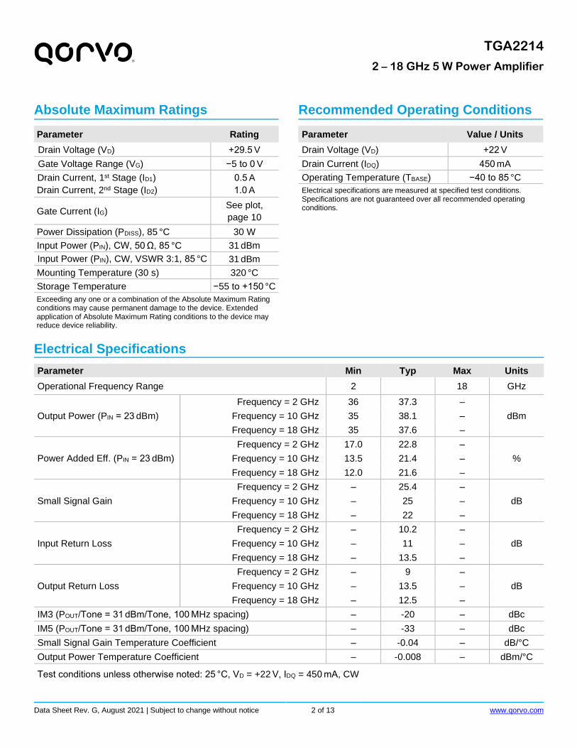
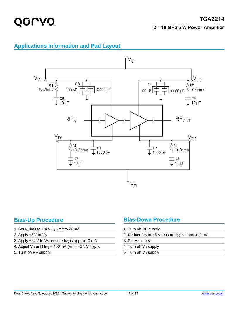
Data Sheet Rev. G, August 2021 | Subject to change without notice 1 of 13 www.qorvo.com
TGA2214
2 – 18 GHz 5 W Power Amplifier ®
Key Features • Frequency Range: 2 – 18 GHz
• POUT: 37 dBm @ PIN = 23 dBm
• PAE: 20 % @ PIN = 23 dBm
• Large Signal Gain (PIN = 23 dBm): 14 dB
• Small Signal Gain: 22 dB
• Return Loss: 7 dB
• Bias: VD = +22 V, IDQ = 450 mA, VG = −2.3 V Typical
• Chip Dimensions: 2.87 x 4.87 x 0.10 mm
• Performance under CW operation
Performance is typical across frequency. Please
reference electrical specification table and data plots for
more details.
Product Overview
Qorvo’s TGA2214 is a wideband power amplifier fabricated
on Qorvo’s QGaN15 GaN on SiC process. The TGA2214
operates from 2 – 18 GHz and achieves 5 W of saturated
output power with 14 dB of large signal gain and greater
than 20 % power-added efficiency.
This combination of wideband power, gain and efficiency
provides system designers the flexibility to improve system
performance while reducing size and cost.
The TGA2214 is matched to 50 Ω with integrated DC
blocking capacitors on both RF ports simplifying system
integration; it is ideally suited for electronic warfare, test
instrumentation and radar applications across both military
and commercial markets.
Lead free and RoHS compliant.
Functional Block Diagram
Applications • Test Equipment
• Electronic Warfare
• Military Radar
Ordering Information
Part No. Description
TGA2214 2 – 18 GHz 5 W GaN Power Amplifier
TGA2214EVB01 TGA2214 Evaluation Board
Data Sheet Rev. G, August 2021 | Subject to change without notice 2 of 13 www.qorvo.com
TGA2214
2 – 18 GHz 5 W Power Amplifier ®
Recommended Operating Conditions
Parameter Value / Units
Drain Voltage (VD) +22 V
Drain Current (IDQ) 450 mA
Operating Temperature (TBASE) −40 to 85 °C
Electrical specifications are measured at specified test conditions. Specifications are not guaranteed over all recommended operating conditions.
Absolute Maximum Ratings
Parameter Rating
Drain Voltage (VD) +29.5 V
Gate Voltage Range (VG) −5 to 0 V
Drain Current, 1st Stage (ID1)
Drain Current, 2nd Stage (ID2)
0.5 A
1.0 A
Gate Current (IG) See plot,
page 10
Power Dissipation (PDISS), 85 °C 30 W
Input Power (PIN), CW, 50 Ω, 85 °C 31 dBm
Input Power (PIN), CW, VSWR 3:1, 85 °C 31 dBm
Mounting Temperature (30 s) 320 °C
Storage Temperature −55 to +150 °C
Exceeding any one or a combination of the Absolute Maximum Rating conditions may cause permanent damage to the device. Extended application of Absolute Maximum Rating conditions to the device may reduce device reliability.
Electrical Specifications Parameter Min Typ Max Units
Operational Frequency Range 2 18 GHz
Output Power (PIN = 23 dBm)
Frequency = 2 GHz 36 37.3 –
dBm Frequency = 10 GHz 35 38.1 –
Frequency = 18 GHz 35 37.6 –
Power Added Eff. (PIN = 23 dBm)
Frequency = 2 GHz 17.0 22.8 –
% Frequency = 10 GHz 13.5 21.4 –
Frequency = 18 GHz 12.0 21.6 –
Small Signal Gain
Frequency = 2 GHz – 25.4 –
dB Frequency = 10 GHz – 25 –
Frequency = 18 GHz – 22 –
Input Return Loss
Frequency = 2 GHz – 10.2 –
dB Frequency = 10 GHz – 11 –
Frequency = 18 GHz – 13.5 –
Output Return Loss
Frequency = 2 GHz – 9 –
dB Frequency = 10 GHz – 13.5 –
Frequency = 18 GHz – 12.5 –
IM3 (POUT/Tone = 31 dBm/Tone, 100 MHz spacing) – -20 – dBc
IM5 (POUT/Tone = 31 dBm/Tone, 100 MHz spacing) – -33 – dBc
Small Signal Gain Temperature Coefficient – -0.04 – dB/°C
Output Power Temperature Coefficient – -0.008 – dBm/°C
Test conditions unless otherwise noted: 25 °C, VD = +22 V, IDQ = 450 mA, CW
Data Sheet Rev. G, August 2021 | Subject to change without notice 3 of 13 www.qorvo.com
TGA2214
2 – 18 GHz 5 W Power Amplifier ®
Performance Plots – Large Signal
Test conditions unless otherwise noted: 25 °C, VD = +22 V, IDQ = 450 mA, CW.
Data Sheet Rev. G, August 2021 | Subject to change without notice 4 of 13 www.qorvo.com
TGA2214
2 – 18 GHz 5 W Power Amplifier ®
Performance Plots – Large Signal
Test conditions unless otherwise noted: 25 °C, VD = +22 V, IDQ = 450 mA, CW.
12
13
14
15
16
17
18
2 4 6 8 10 12 14 16 18
Gain
(dB
)
Frequency (GHz)
Power Gain vs. Frequency vs. VD
Pin = 23 dBm, Temp = 25 °C
22 V
20 V
Data Sheet Rev. G, August 2021 | Subject to change without notice 5 of 13 www.qorvo.com
TGA2214
2 – 18 GHz 5 W Power Amplifier ®
Performance Plots – Large Signal
Test conditions unless otherwise noted: 25 °C, VD = +22 V, IDQ = 450 mA, CW.
Data Sheet Rev. G, August 2021 | Subject to change without notice 6 of 13 www.qorvo.com
TGA2214
2 – 18 GHz 5 W Power Amplifier ®
Performance Plots – Linearity
Test conditions unless otherwise noted: 25 °C, VD = +22 V, IDQ = 450 mA, CW.
Data Sheet Rev. G, August 2021 | Subject to change without notice 7 of 13 www.qorvo.com
TGA2214
2 – 18 GHz 5 W Power Amplifier ®
Performance Plots – Small Signal
Test conditions unless otherwise noted: 25 °C, VD = +22 V, IDQ = 450 mA, CW.
18
20
22
24
26
28
30
1 3 5 7 9 11 13 15 17 19
S21 (
dB
)
Frequency (GHz)
Gain vs. Frequency vs. Temperature
-40 °C
25 °C
85 °C
Data Sheet Rev. G, August 2021 | Subject to change without notice 8 of 13 www.qorvo.com
TGA2214
2 – 18 GHz 5 W Power Amplifier ®
Thermal and Reliability Information Parameter Test Conditions Value Units
Thermal Resistance (θJC) (1) TBASE = 85 °C, Freq = 9.5 GHz, VD = 22 V, PIN = 23 dBm, IDQ = 450 mA, IDRIVE = 1.28 A, POUT = 37.5 dBm, PDISS = 22.7 W
3.921 °C / W
Channel Temperature TCH (Quiescent) (1,2) 174 °C
Notes:
1. Die mounted to 20 mil CuMo carrier plate with eutectic die attach. Thermal resistance determined to the back of carrier (85 °C).
2. IR Scan equivalent temperature. Refer to the following document: GaN Device Channel Temperature, Thermal Resistance, and Reliability Estimates
Power Dissipation and Maximum Gate Current
Data Sheet Rev. G, August 2021 | Subject to change without notice 9 of 13 www.qorvo.com
TGA2214
2 – 18 GHz 5 W Power Amplifier ®
Applications Information and Pad Layout
Bias-Up Procedure Bias-Down Procedure
1. Set ID limit to 1.4 A, IG limit to 20 mA 1. Turn off RF supply
2. Apply −5 V to VG 2. Reduce VG to −5 V; ensure IDQ is approx. 0 mA
3. Apply +22 V to VD; ensure IDQ is approx. 0 mA 3. Set VD to 0 V
4. Adjust VG until IDQ = 450 mA (VG ~ −2.3 V Typ.). 4. Turn off VD supply
5. Turn on RF supply 5. Turn off VG supply
Data Sheet Rev. G, August 2021 | Subject to change without notice 10 of 13 www.qorvo.com
TGA2214
2 – 18 GHz 5 W Power Amplifier ®
Evaluation Board (EVB) Layout Assembly
Bill of Materials Reference Des. Value Description Manuf. Part Number
C1, C2 1000 pF Cap, +50 V, 10 %, SLCC Presidio MSA3535B102K2H5C-F
C3, C4 100 pF // 10000 pF
Cap, +50 V, 20 %, X7R, MLCC Presidio MVB3030X103M2H5C1F
C5, C6, C7, C8 10 F Cap, 1206, 20 %, +50 V, X5R Various –
R1, R2, R3, R4 10 Ohms Res, 0402, 5 % Various –
Data Sheet Rev. G, August 2021 | Subject to change without notice 11 of 13 www.qorvo.com
TGA2214
2 – 18 GHz 5 W Power Amplifier ®
Mechanical Information and Bond Pad Description
Units: millimeters Thickness: 0.100
Die x,y size tolerance: ± 0.008 Ground is backside of die
Bond Pad Description Pad No. Symbol Pad Size (mm) Description
1 RF IN 0.150 x 0.200 RF Input; matched to 50 Ω, DC blocked
2 VG1 (1) 0.200 x 0.100
Gate voltage for stage 1, bias network is required; see Application Circuit on page 9 as an example.
3 VG2 (1) 0.200 x 0.200
Gate voltage for stage 2, bias network is required; see Application Circuit on page 9 as an example.
4 RF OUT 0.150 x 0.200 RF Output; matched to 50 Ω, DC blocked
5 VD2 (2) 0.400 x 0.200
Drain voltage for stage 2, bias network is required; see Application Circuit on page 9 as an example
6 VD1 (2) 0.300 x 0.125
Drain voltage for stage 1, bias network is required; see Application Circuit on page 9 as an example
Notes:
1) VG1 & VG2 may be tied together off-chip.
2) VD1 & VD2 may be tied together off-chip.
2 3
1 4
6 5
Data Sheet Rev. G, August 2021 | Subject to change without notice 12 of 13 www.qorvo.com
TGA2214
2 – 18 GHz 5 W Power Amplifier ®
Assembly Notes
Component placement and die attachment assembly notes:
• Vacuum pencils and/or vacuum collets are the preferred method of pick up.
• Air bridges must be avoided during placement.
• The force impact is critical during auto placement.
• Conductive epoxy attachment may be used for small-signal low power dissipation die.
• Follow manufacture instructions for epoxy curing.
Reflow process assembly notes:
• Use AuSn (80/20) solder and limit exposure to temperatures above 300°C to 3-4 minutes, maximum.
• An alloy station or conveyor furnace with reducing atmosphere should be used.
• Do not use any kind of flux.
• Coefficient of thermal expansion matching is critical for long-term reliability.
• Devices must be stored in a dry nitrogen atmosphere.
Interconnect process assembly notes:
• Thermosonic ball bonding is the preferred interconnect technique.
• Force, time, and ultrasonic are critical parameters.
• Aluminum wire should not be used.
• Devices with small pad sizes should be bonded with 0.0007-inch wire.
Data Sheet Rev. G, August 2021 | Subject to change without notice 13 of 13 www.qorvo.com
TGA2214
2 – 18 GHz 5 W Power Amplifier ®
Handling Precautions Parameter Rating Standard
Caution! ESD-Sensitive Device ESD – Human Body Model (HBM) 1B ANSI/ESD/JEDEC JS-001
RoHS Compliance This part is compliant with 2011/65/EU RoHS directive (Restrictions on the Use of Certain Hazardous Substances in Electrical and Electronic Equipment) as amended by Directive 2015/863/EU. This product also has the following attributes:
• Lead Free
• Halogen Free (Chlorine, Bromine) • Antimony Free
• TBBP-A (C15H12Br402) Free
• SVHC Free
• PFOS Free
Contact Information For the latest specifications, additional product information, worldwide sales and distribution locations:
Web: www.qorvo.com
Tel: 1-844-890-8163
Email: [email protected]
Important Notice
The information contained in this Data Sheet and any associated documents (“Data Sheet Information”) is believed to be reliable; however, Qorvo makes no warranties regarding the Data Sheet Information and assumes no responsibility or liability whatsoever for the use of said information. All Data Sheet Information is subject to change without notice. Customers should obtain and verify the latest relevant Data Sheet Information before placing orders for Qorvo® products. Data Sheet Information or the use thereof does not grant, explicitly, implicitly or otherwise any rights or licenses to any third party with respect to patents or any other intellectual property whether with regard to such Data Sheet Information itself or anything described by such information. DATA SHEET INFORMATION DOES NOT CONSTITUTE A WARRANTY WITH RESPECT TO THE PRODUCTS DESCRIBED HEREIN, AND QORVO HEREBY DISCLAIMS ANY AND ALL WARRANTIES WITH RESPECT TO SUCH PRODUCTS WHETHER EXPRESS OR IMPLIED BY LAW, COURSE OF DEALING, COURSE OF PERFORMANCE, USAGE OF TRADE OR OTHERWISE, INCLUDING THE IMPLIED WARRANTIES OF MERCHANTABILITY AND FITNESS FOR A PARTICULAR PURPOSE. Without limiting the generality of the foregoing, Qorvo® products are not warranted or authorized for use as critical components in medical, life-saving, or life-sustaining applications, or other applications where a failure would reasonably be expected to cause severe personal injury or death. Applications described in the Data Sheet Information are for illustrative purposes only. Customers are responsible for validating that a particular product described in the Data Sheet Information is suitable for use in a particular application. © 2021 Qorvo US, Inc. All rights reserved. This document is subject to copyright laws in various jurisdictions worldwide and may not be reproduced or distributed, in whole or in part, without the express written consent of Qorvo US, Inc. | QORVO® is a registered trademark of Qorvo US, Inc.
Mouser Electronics
Authorized Distributor
Click to View Pricing, Inventory, Delivery & Lifecycle Information: Qorvo:
TGA2214