24

PRODUCT SPECIFICATION KPS-0035-A02
E-mail: [email protected] http:// www.visionox.com 2 / 24
CONTENT
REVISION RECORD ....................................................................................................................................................3
1 OVERVIEW ..........................................................................................................................................................4
2 FEATURES............................................................................................................................................................4
3 MECHANICAL DATA .........................................................................................................................................4
4 MECHANICAL DRAWING ................................................................................................................................5
5 MODULE INTERFACE.......................................................................................................................................6
6 FUNCTION BLOCK DIAGRAM .......................................................................................................................7
6.1 FUNCTION BLOCK DIAGRAM...............................................................................................................................7
6.2 PANEL LAYOUT DIAGRAM ...................................................................................................................................7
7 ABSOLUTE MAXIMUM RATINGS..................................................................................................................8
8 ELECTRICAL CHARACTERISTICS...............................................................................................................8
8.1 DC ELECTRICAL CHARACTERISTICS ...................................................................................................................8
8.2 ELECTRO-OPTICAL CHARACTERISTICS ................................................................................................................9
8.3 AC ELECTRICAL CHARACTERISTICS .................................................................................................................10
9 FUNCTIONAL SPECIFICATION AND APPLICATION CIRCUIT............................................................14
9.1 POWER ON AND POWER OFF SEQUENCE..........................................................................................................14
9.2 APPLICATION CIRCUIT.......................................................................................................................................15
9.3 DISPLAY CONTROL INSTRUCTION......................................................................................................................16
9.4 RECOMMENDED SOFTWARE INITIALIZATION .....................................................................................................16
10 PACKAGE SPECIFICATION...........................................................................................................................17
11 RELIABILITY ....................................................................................................................................................18
11.1 RELIABILITY TEST.............................................................................................................................................18
11.2 LIFETIME...........................................................................................................................................................18
11.3 FAILURE CHECK STANDARD..............................................................................................................................18
12 ILLUSTRATION OF OLED PRODUCT NAME ............................................................................................19
13 OUTGOING QUALITY CONTROL SPECIFICATIONS..............................................................................20
13.1 SAMPLING METHOD ..........................................................................................................................................20
13.2 INSPECTION CONDITIONS ..................................................................................................................................20
13.3 QUALITY ASSURANCE ZONES............................................................................................................................20
13.4 INSPECTION STANDARD.....................................................................................................................................21
14 PRECAUTIONS FOR OPERATION AND STORAGE..................................................................................23
14.1 PRECAUTIONS FOR OPERATION .........................................................................................................................23
14.2 SOLDERING .......................................................................................................................................................24
14.3 PRECAUTIONS FOR STORAGE.............................................................................................................................24
14.4 WARRANTY PERIOD ...........................................................................................................................................24
PRODUCT SPECIFICATION KPS-0035-A02
E-mail: [email protected] http:// www.visionox.com 3 / 24
REVISION RECORD
REV. REVISION DESCRIPTION REV. DATE REMARK
E01 Initial Release 2009-02-23
Y01 Updata content 2009-03-18
A01
Add the information of module weight. Add the information of electro-optical characteristics. Add the information of recommended software initialization. Add the information of operating lifetime.
2009-05-11
Page 4 Page 9 Page 16 Page 18
A02 Updata Pin define 2009-07-07 Page 6
PRODUCT SPECIFICATION KPS-0035-A02
E-mail: [email protected] http:// www.visionox.com 4 / 24
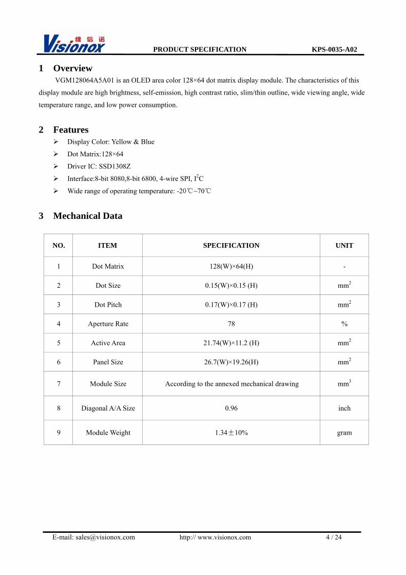
1 Overview VGM128064A5A01 is an OLED area color 128×64 dot matrix display module. The characteristics of this
display module are high brightness, self-emission, high contrast ratio, slim/thin outline, wide viewing angle, wide
temperature range, and low power consumption.
2 Features Display Color: Yellow & Blue
Dot Matrix:128×64
Driver IC: SSD1308Z
Interface:8-bit 8080,8-bit 6800, 4-wire SPI, I2C
Wide range of operating temperature: -20~70
3 Mechanical Data
NO. ITEM SPECIFICATION UNIT
1 Dot Matrix 128(W)×64(H) -
2 Dot Size 0.15(W)×0.15 (H) mm2
3 Dot Pitch 0.17(W)×0.17 (H) mm2
4 Aperture Rate 78 %
5 Active Area 21.74(W)×11.2 (H) mm2
6 Panel Size 26.7(W)×19.26(H) mm2
7 Module Size According to the annexed mechanical drawing mm3
8 Diagonal A/A Size 0.96 inch
9 Module Weight 1.34±10% gram
PRODUCT SPECIFICATION KPS-0035-A02
E-mail: [email protected] http:// www.visionox.com 5 / 24
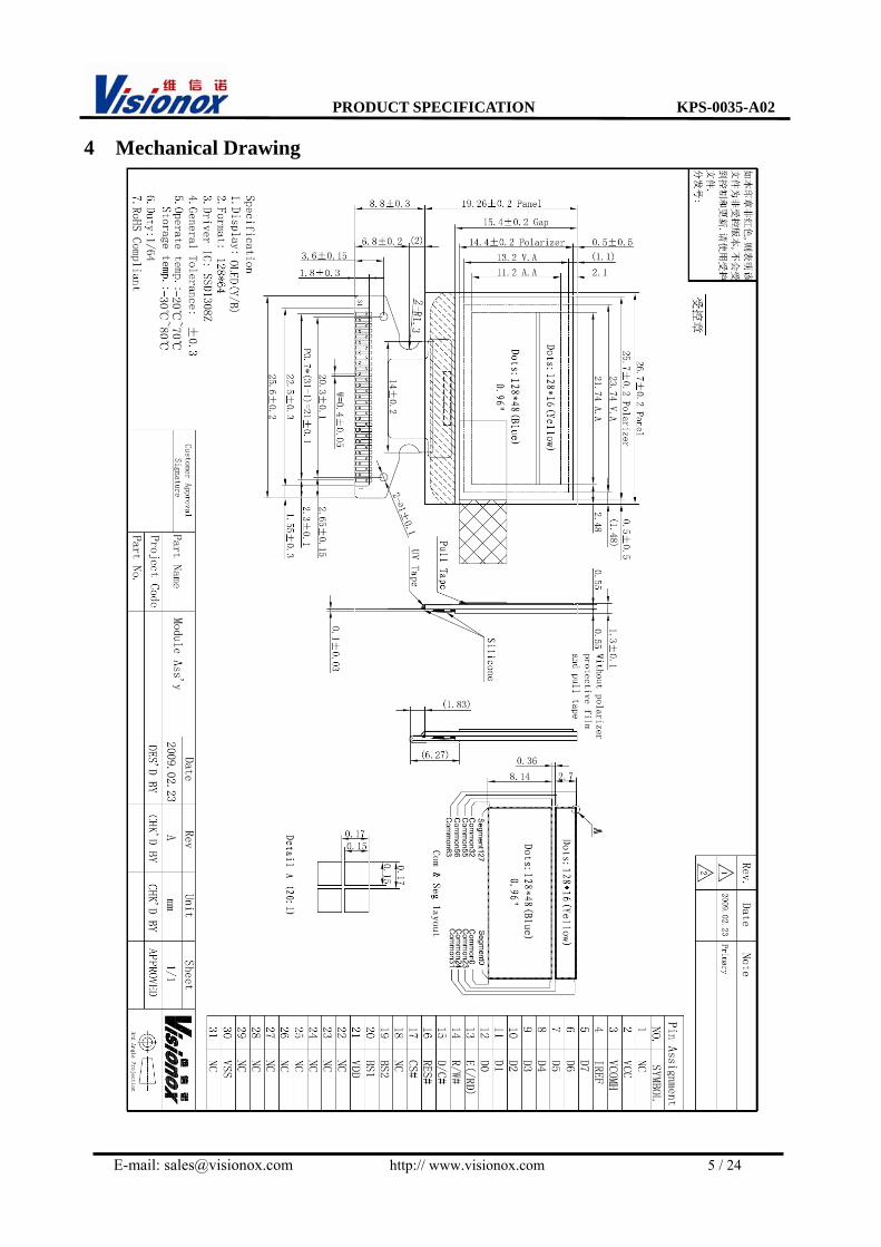
4 Mechanical Drawing
PRODUCT SPECIFICATION KPS-0035-A02
E-mail: [email protected] http:// www.visionox.com 6 / 24
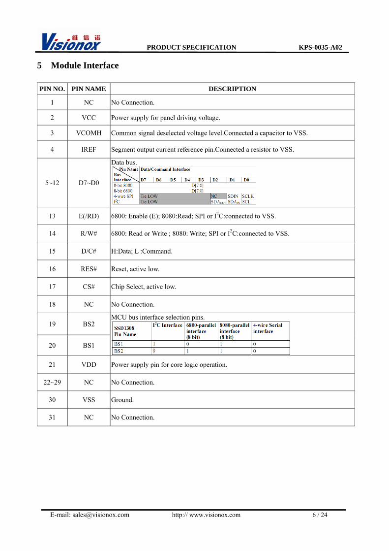
5 Module Interface PIN NO. PIN NAME DESCRIPTION
1 NC No Connection.
2 VCC Power supply for panel driving voltage.
3 VCOMH Common signal deselected voltage level.Connected a capacitor to VSS.
4 IREF Segment output current reference pin.Connected a resistor to VSS.
5~12 D7~D0
Data bus.
13 E(/RD) 6800: Enable (E); 8080:Read; SPI or I2C:connected to VSS.
14 R/W# 6800: Read or Write ; 8080: Write; SPI or I2C:connected to VSS.
15 D/C# H:Data; L :Command.
16 RES# Reset, active low.
17 CS# Chip Select, active low.
18 NC No Connection.
19 BS2
20 BS1
MCU bus interface selection pins.
21 VDD Power supply pin for core logic operation.
22~29 NC No Connection.
30 VSS Ground.
31 NC No Connection.
PRODUCT SPECIFICATION KPS-0035-A02
E-mail: [email protected] http:// www.visionox.com 7 / 24
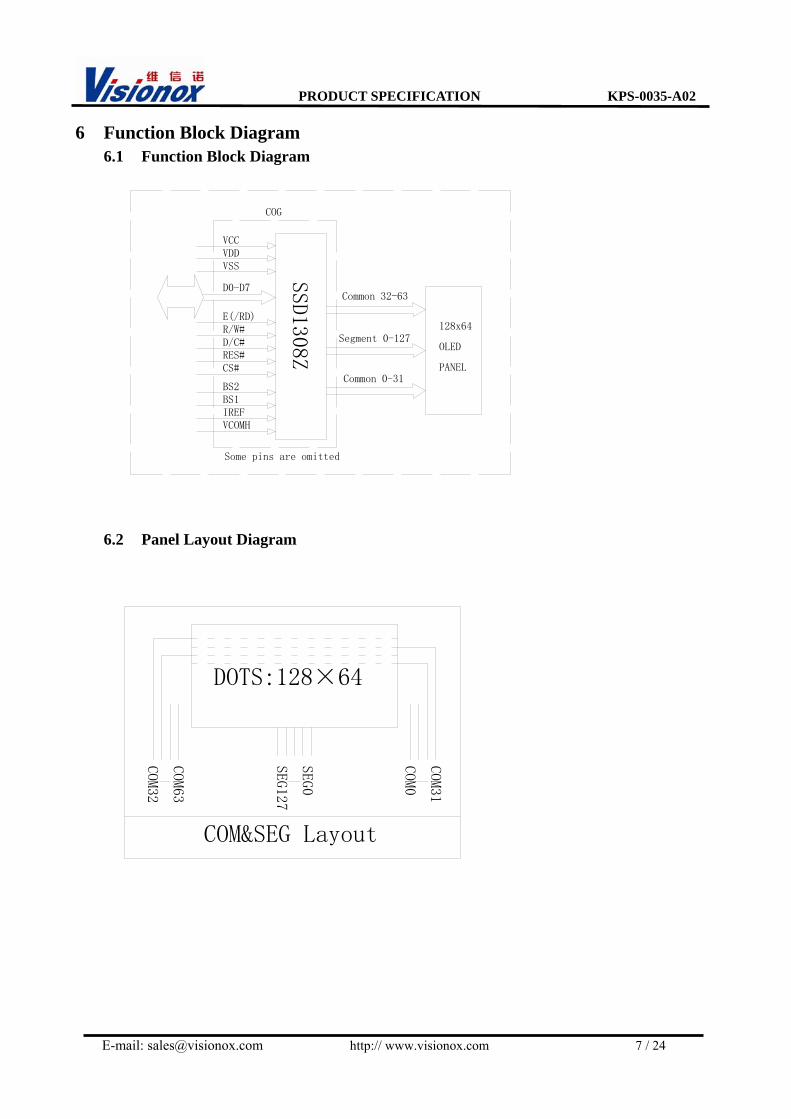
6 Function Block Diagram 6.1 Function Block Diagram
COG
VCOMHIREFBS1BS2
D0-D7
CS#RES#D/C#R/W#
VSSVDDVCC
Common 0-31
Common 32-63
PANEL
OLED
Some pins are omitted
SSD1308Z
Segment 0-127128x64
E(/RD)
6.2 Panel Layout Diagram
COM&SEG Layout
COM31
COM0
COM63
COM32
DOTS:128×64
SEG0
SEG127
PRODUCT SPECIFICATION KPS-0035-A02
E-mail: [email protected] http:// www.visionox.com 8 / 24
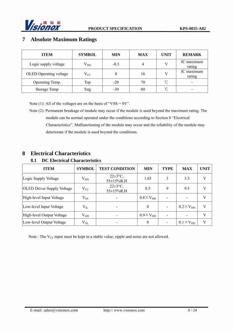
7 Absolute Maximum Ratings
ITEM SYMBOL MIN MAX UNIT REMARK
Logic supply voltage VDD -0.3 4 V IC maximum rating
OLED Operating voltage VCC 0 16 V IC maximum rating
Operating Temp. Top -20 70 -
Storage Temp Tstg -30 80 -
Note (1): All of the voltages are on the basis of “VSS = 0V”.
Note (2): Permanent breakage of module may occur if the module is used beyond the maximum rating. The
module can be normal operated under the conditions according to Section 8 “Electrical
Characteristics”. Malfunctioning of the module may occur and the reliability of the module may
deteriorate if the module is used beyond the conditions.
8 Electrical Characteristics 8.1 DC Electrical Characteristics
ITEM SYMBOL TEST CONDITION MIN TYPE MAX UNIT
Logic Supply Voltage VDD 22±3°C, 55±15%R.H 1.65 3 3.3 V
OLED Driver Supply Voltage VCC 22±3°C, 55±15%R.H 8.5 9 9.5 V
High-level Input Voltage VIH - 0.8×VDD - - V
Low-level Input Voltage VIL - 0 - 0.2×VDD V
High-level Output Voltage VOH - 0.9×VDD - - V
Low-level Output Voltage VOL - 0 - 0.1×VDD V
Note : The VCC input must be kept in a stable value; ripple and noise are not allowed.
PRODUCT SPECIFICATION KPS-0035-A02
E-mail: [email protected] http:// www.visionox.com 9 / 24
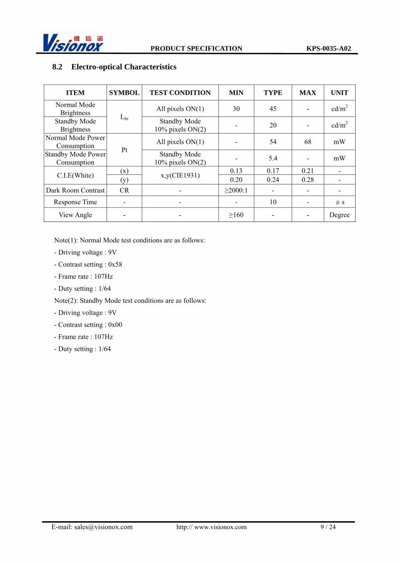
8.2 Electro-optical Characteristics
ITEM SYMBOL TEST CONDITION MIN TYPE MAX UNIT
Normal Mode Brightness All pixels ON(1) 30 45 - cd/m2
Standby Mode Brightness
Lbr Standby Mode 10% pixels ON(2) - 20 - cd/m2
Normal Mode Power Consumption All pixels ON(1) - 54 68 mW
Standby Mode Power Consumption
Pt Standby Mode 10% pixels ON(2) - 5.4 - mW
(x) 0.13 0.17 0.21 - C.I.E(White) (y) x,y(CIE1931) 0.20 0.24 0.28 -
Dark Room Contrast CR - ≥2000:1 - - -
Response Time - - - 10 - μs
View Angle - - ≥160 - - Degree
Note(1): Normal Mode test conditions are as follows:
- Driving voltage : 9V
- Contrast setting : 0x58
- Frame rate : 107Hz
- Duty setting : 1/64
Note(2): Standby Mode test conditions are as follows:
- Driving voltage : 9V
- Contrast setting : 0x00
- Frame rate : 107Hz
- Duty setting : 1/64
PRODUCT SPECIFICATION KPS-0035-A02
E-mail: [email protected] http:// www.visionox.com 10 / 24
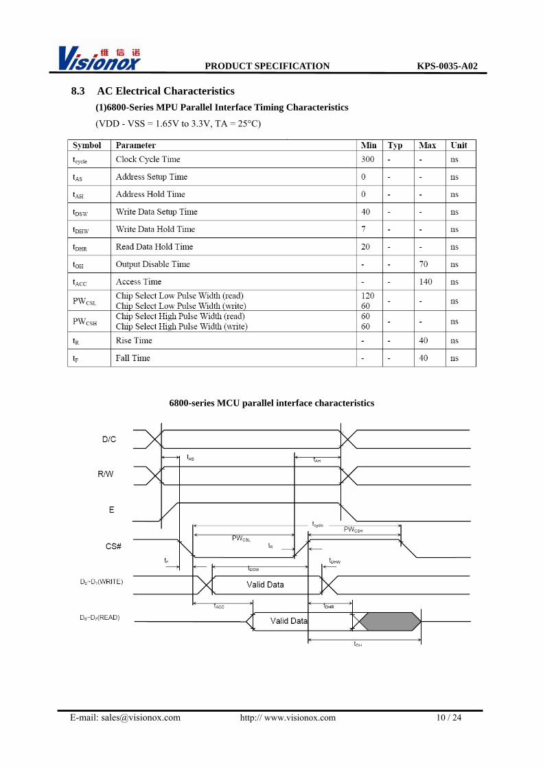
8.3 AC Electrical Characteristics (1)6800-Series MPU Parallel Interface Timing Characteristics
(VDD - VSS = 1.65V to 3.3V, TA = 25°C)
6800-series MCU parallel interface characteristics
PRODUCT SPECIFICATION KPS-0035-A02
E-mail: [email protected] http:// www.visionox.com 11 / 24
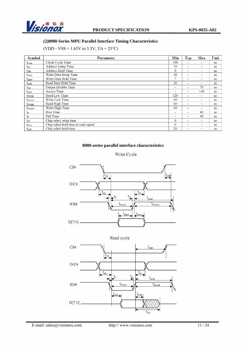
(2)8080-Series MPU Parallel Interface Timing Characteristics (VDD - VSS = 1.65V to 3.3V, TA = 25°C)
8080-series parallel interface characteristics
PRODUCT SPECIFICATION KPS-0035-A02
E-mail: [email protected] http:// www.visionox.com 12 / 24
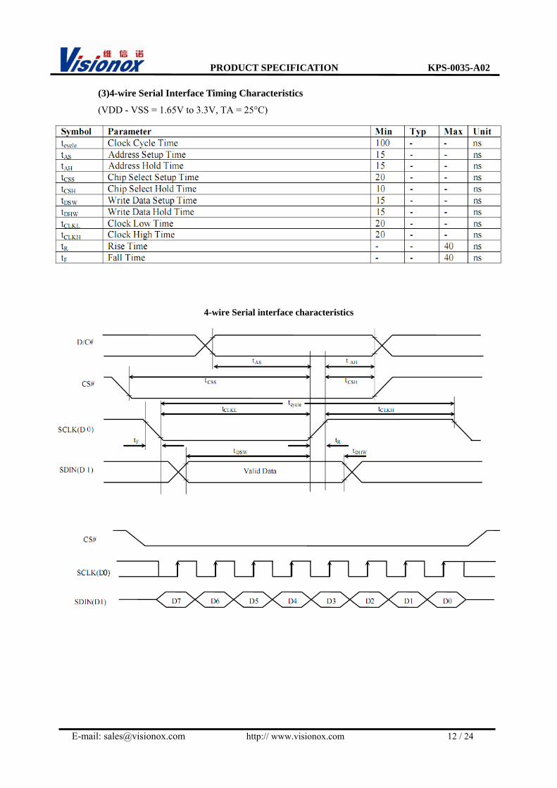
(3)4-wire Serial Interface Timing Characteristics
(VDD - VSS = 1.65V to 3.3V, TA = 25°C)
4-wire Serial interface characteristics
PRODUCT SPECIFICATION KPS-0035-A02
E-mail: [email protected] http:// www.visionox.com 13 / 24
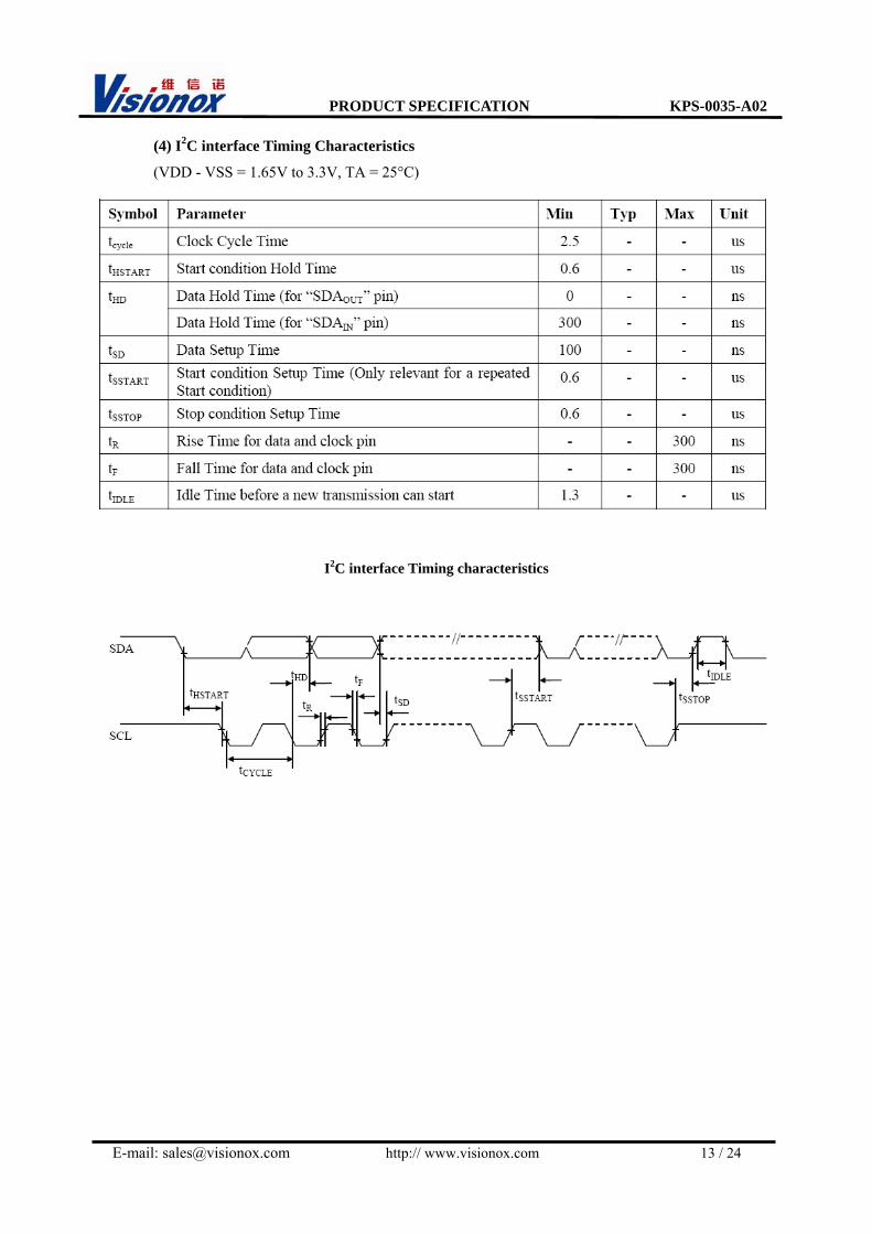
(4) I2C interface Timing Characteristics
(VDD - VSS = 1.65V to 3.3V, TA = 25°C)
I2C interface Timing characteristics

PRODUCT SPECIFICATION KPS-0035-A02
E-mail: [email protected] http:// www.visionox.com 14 / 24
9 Functional Specification and Application Circuit 9.1 Power ON and Power OFF Sequence
Power ON Sequence:
1. Power ON VDD
2. After VDD become stable, set RES# pin LOW (logic low) for at least 3us (t1)(4) and then HIGH
(logic high).
3. After set RES# pin LOW (logic low), wait for at least 3us (t2). Then Power ON VCC(1)
.
4. After VCC become stable, send command AFh for display ON. SEG/COM will be ON after 100ms(tAF).
Power OFF Sequence:
1. Send command AEh for display OFF.
2. Power OFF VCC(1),(2),(3).
3. Power OFF VDD after tOFF. (5) (Typical tOFF=100ms)
Note:
(1)Since an ESD protection circuit is connected between VDD and VCC, VCC becomes lower than VDD
whenever VDD is ON and VCC is OFF as shown in the dotted line of VCC in above figures.
(2) VCC should be kept float (disable) when it is OFF.
(3) Power Pins(VDD, VCC) can never be pulled to ground under any circumstance.
(4) The register values are reset after t1.
(5) VDD should not be Power OFF before VCC Power OFF
PRODUCT SPECIFICATION KPS-0035-A02
E-mail: [email protected] http:// www.visionox.com 15 / 24
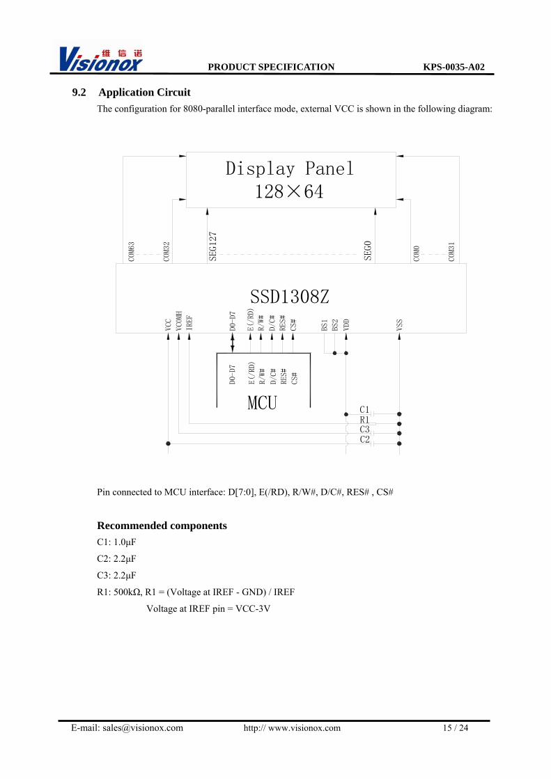
9.2 Application Circuit The configuration for 8080-parallel interface mode, external VCC is shown in the following diagram:
R1
C2C3
C1
VCC
VCOMH
IREF
D0-D7
D/C#
RES#
CS#
BS2
BS1
VDD
VSS
COM31
COM0
COM32
COM63
MCU
CS#
RES#
D/C#
D0-
D7
R/W#
R/W#
Display Panel128×64
SSD1308Z
E(/R
D)E(/
RD)
SEG127
SEG0
Pin connected to MCU interface: D[7:0], E(/RD), R/W#, D/C#, RES# , CS#
Recommended components
C1: 1.0μF
C2: 2.2μF
C3: 2.2μF
R1: 500kΩ, R1 = (Voltage at IREF - GND) / IREF
Voltage at IREF pin = VCC-3V
PRODUCT SPECIFICATION KPS-0035-A02
E-mail: [email protected] http:// www.visionox.com 16 / 24
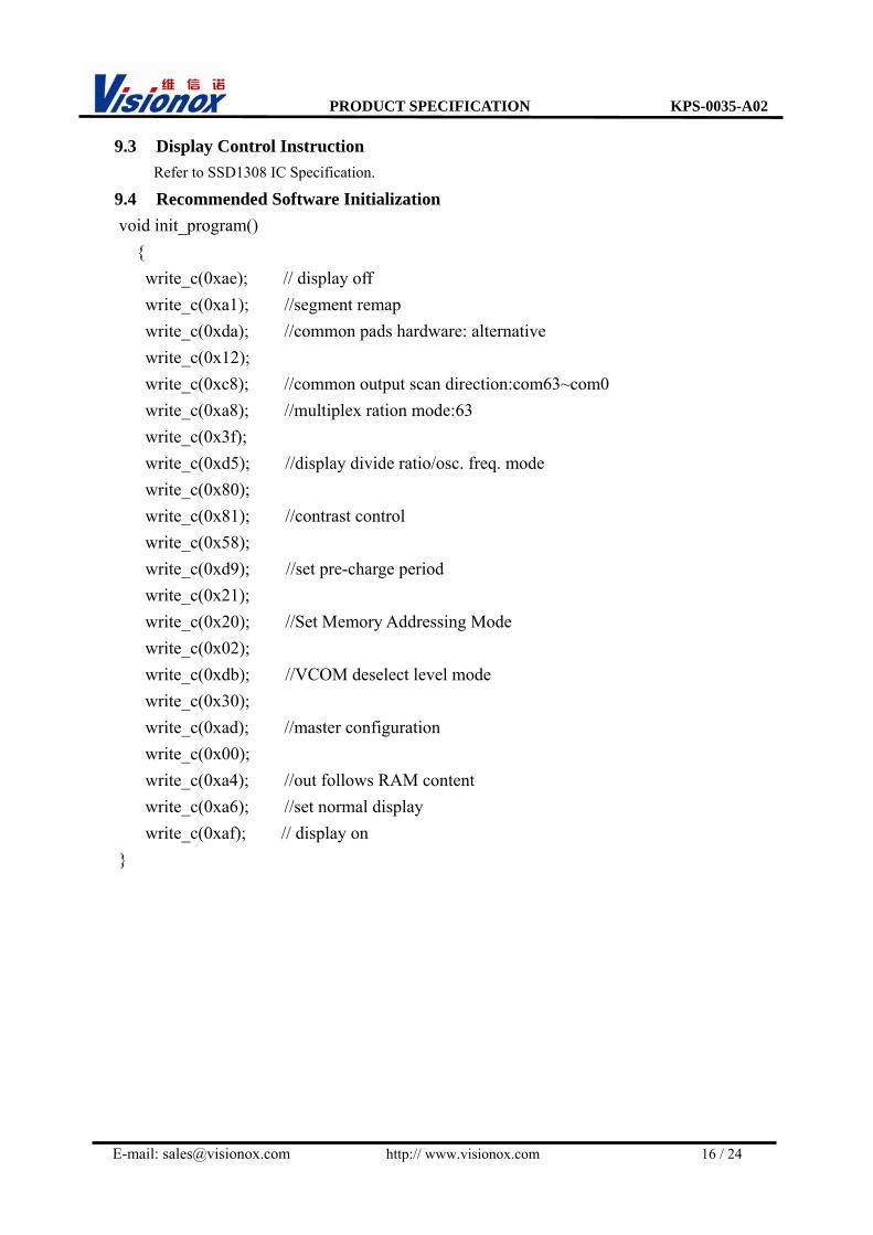
9.3 Display Control Instruction Refer to SSD1308 IC Specification.
9.4 Recommended Software Initialization void init_program() write_c(0xae); // display off write_c(0xa1); //segment remap write_c(0xda); //common pads hardware: alternative write_c(0x12); write_c(0xc8); //common output scan direction:com63~com0 write_c(0xa8); //multiplex ration mode:63 write_c(0x3f); write_c(0xd5); //display divide ratio/osc. freq. mode write_c(0x80); write_c(0x81); //contrast control write_c(0x58); write_c(0xd9); //set pre-charge period write_c(0x21); write_c(0x20); //Set Memory Addressing Mode write_c(0x02); write_c(0xdb); //VCOM deselect level mode write_c(0x30); write_c(0xad); //master configuration write_c(0x00); write_c(0xa4); //out follows RAM content write_c(0xa6); //set normal display write_c(0xaf); // display on

PRODUCT SPECIFICATION KPS-0035-A02
E-mail: [email protected] http:// www.visionox.com 17 / 24
10 Package Specification
*5
create a power vacuum
add five desiccants
package with plastic bags
fix tr
ays wit
h tape
small carton package
NOTE:Tape on the small carton & big carton
28 contained trays, 2 empty
( 9 )
2 small cartons in 1 big carton
Package finished
( 8 )
( 4 )
( 7 )
( 3 )
Package
quant
ity pro
ducts:
( 6 )
normal
1
( 2 )
180° revers
2
370*273
t=0.
8mm
( 5 )
( 1 )Tray:
TRAY
Package order(1)~(9)
Add
EPE in
every
contain
ed tray
order 1、 2、 1、 2
EPE
672 pc
s of 1
small
carton
1 tray
contai
n 48 p
cs14 c
ontaine
d tray
s, 1 em
pty tr
ay
trays,
Package quantity products:
1344 pcs of 1 big carton
L425*W330*L175 mm
L450*W350*L360 mm

PRODUCT SPECIFICATION KPS-0035-A02
E-mail: [email protected] http:// www.visionox.com 18 / 24
11 Reliability 11.1 Reliability Test
NO. ITEM CONDITION QUANTITY
1 High Temperature (Non-operation) 80,240hrs 4
2 Low Temperature (Non-operation) -30,240hrs 4
3 High Temperature (Operation) 70,240hrs 4
4 Low Temperature (Operation) -20,240hrs 4
5 High Temperature / High Humidity (Operation)
60,90%RH,240hrs 4
6 Thermal shock (Non-operation)
-30~80(-30/30min;transit/3min;80/30min;transit/3min) 1cycle: 66min,30cycles 4
7 Vibration
Frequency: 5~50Hz,0.5G Scan rate: 1 oct/min Time: 2 hrs/axis Test axis: X,Y, Z
1 Carton
8 Drop Height: 100 cm Sequence: 1 angle, 3 edges and 6 faces 1 Carton
Test and measurement conditions 1. All measurements shall not be started until the specimens attain to temperature stability, the stable
time is at least 15 minutes.
2. The degradation of polarizer is ignored for item 5.
3.The tolerance of temperature is ±3, and the tolerance of relative humidity is ±5%.
Evaluation criteria 1. The function test is OK.
2. No observable defects.
3. Luminance:≥50% of initial value.
4. Current consumption: within ± 50% of initial value.
11.2 Lifetime End of lifetime is specified as 50% of initial brightness and the test pattern at operating condition is
50% alternating checkerboard.
ITEM MIN MAX UNIT CONDITION
Operation Life Time 20000 - hrs 45 cd/m2,50% Checkerboard
An average operating lifetime of more than 10,000 hrs (checkerboard) at room temperature is
approached by 240 hrs @ 80°C operating.
11.3 Failure Check Standard After the completion of the described reliability test, the samples were left at room temperature for 2
hrs prior to conducting the failure test at 22±3°C; 55±15% RH.
PRODUCT SPECIFICATION KPS-0035-A02
E-mail: [email protected] http:// www.visionox.com 19 / 24
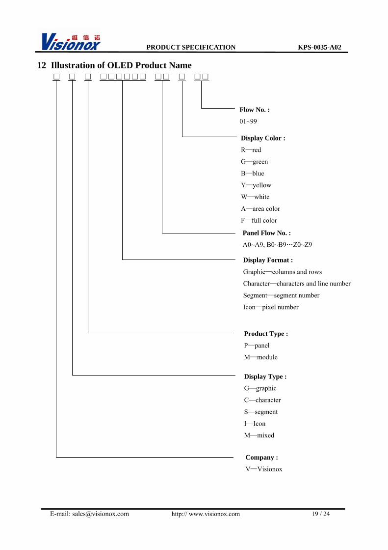
12 Illustration of OLED Product Name
Company :
V—Visionox
Display Type :
G—graphic
C—character
S—segment
I—Icon
M—mixed
Product Type :
P—panel
M—module
Display Format :
Graphic—columns and rows
Character—characters and line number
Segment—segment number
Icon—pixel number
Panel Flow No. :
A0~A9, B0~B9…Z0~Z9
Display Color :
R—red
G—green
B—blue
Y—yellow
W—white
A—area color
F—full color
Flow No. :
01~99
PRODUCT SPECIFICATION KPS-0035-A02
E-mail: [email protected] http:// www.visionox.com 20 / 24
13 Outgoing Quality Control Specifications
13.1 Sampling Method (1) GB/T 2828.1-2003/ISO2859-1:1999, inspection level , normal inspeⅡ ction, single sample
inspection
(2) AQL: Major 0.65; Minor 1.0
13.2 Inspection Conditions
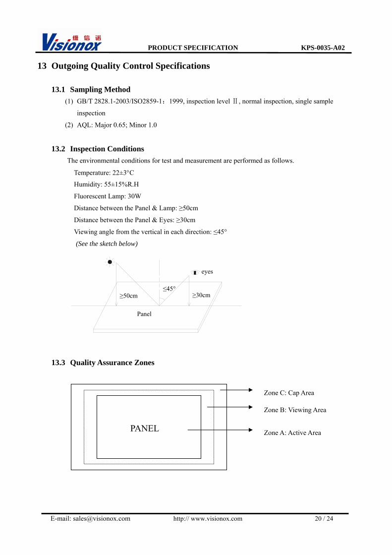
The environmental conditions for test and measurement are performed as follows.
Temperature: 22±3°C
Humidity: 55±15%R.H
Fluorescent Lamp: 30W
Distance between the Panel & Lamp: ≥50cm
Distance between the Panel & Eyes: ≥30cm
Viewing angle from the vertical in each direction: ≤45°
(See the sketch below)
≥30cm≥50cm≤45°
Panel
eyes
13.3 Quality Assurance Zones
Zone C: Cap Area
Zone B: Viewing Area
Zone A: Active Area PANEL
PRODUCT SPECIFICATION KPS-0035-A02
E-mail: [email protected] http:// www.visionox.com 21 / 24
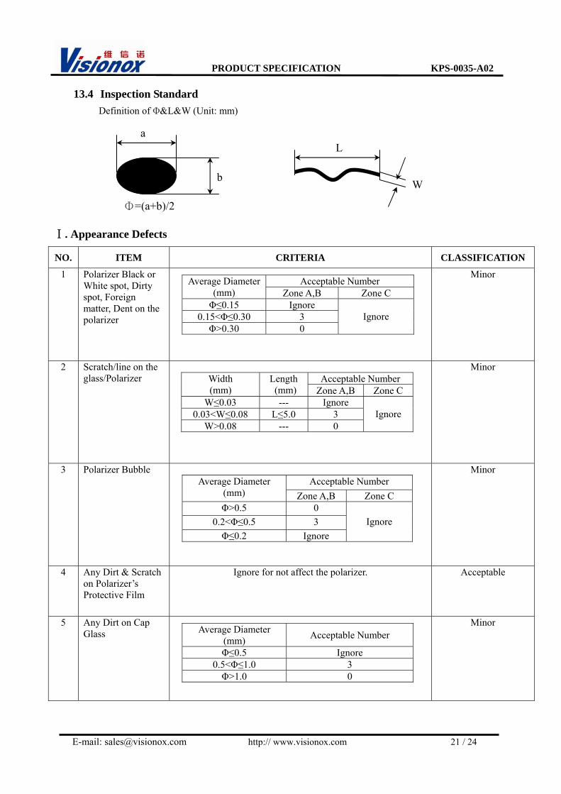
13.4 Inspection Standard Definition of Φ&L&W (Unit: mm)
. Appearance DefectsⅠ
NO. ITEM CRITERIA CLASSIFICATION
1 Polarizer Black or White spot, Dirty spot, Foreign matter, Dent on the polarizer
Acceptable Number Average Diameter
(mm) Zone A,B Zone C Φ≤0.15 Ignore
0.15<Φ≤0.30 3 Φ>0.30 0
Ignore
Minor
2 Scratch/line on the glass/Polarizer
Acceptable Number Width
(mm) Length
(mm) Zone A,B Zone C W≤0.03 --- Ignore
0.03<W≤0.08 L≤5.0 3 W>0.08 --- 0
Ignore
Minor
3 Polarizer Bubble Acceptable Number Average Diameter
(mm) Zone A,B Zone C Φ>0.5 0
0.2<Φ≤0.5 3 Φ≤0.2 Ignore
Ignore
Minor
4 Any Dirt & Scratch on Polarizer’s Protective Film
Ignore for not affect the polarizer. Acceptable
5 Any Dirt on Cap Glass
Average Diameter
(mm) Acceptable Number
Φ≤0.5 Ignore 0.5<Φ≤1.0 3 Φ>1.0 0
Minor
Φ=(a+b)/2
a
b W
L
PRODUCT SPECIFICATION KPS-0035-A02
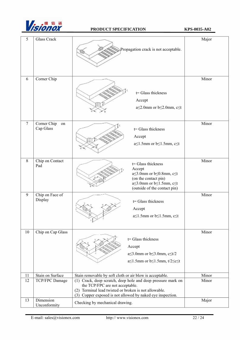
E-mail: [email protected] http:// www.visionox.com 22 / 24
5 Glass Crack
Major
6 Corner Chip
Minor
7 Corner Chip on Cap Glass
Minor
8 Chip on Contact Pad
Minor
9 Chip on Face of Display
Minor
10 Chip on Cap Glass
Minor
11 Stain on Surface Stain removable by soft cloth or air blow is acceptable. Minor 12 TCP/FPC Damage (1) Crack, deep scratch, deep hole and deep pressure mark on
the TCP/FPC are not acceptable. (2) Terminal lead twisted or broken is not allowable. (3) Copper exposed is not allowed by naked eye inspection.
Minor
13 Dimension Unconformity Checking by mechanical drawing. Major
t= Glass thickness Accept a≤3.0mm or b≤0.8mm, c≤t (on the contact pin) a≤3.0mm or b≤1.5mm, c≤t (outside of the contact pin)
t= Glass thickness
Accept
a≤1.5mm or b≤1.5mm, c≤t
t= Glass thickness
Accept
a≤2.0mm or b≤2.0mm, c≤t
t= Glass thickness
Accept
a≤1.5mm or b≤1.5mm, c≤t
t= Glass thickness
Accept
a≤3.0mm or b≤3.0mm, c≤t/2
a≤1.5mm or b≤1.5mm, t/2≤c≤t
Propagation crack is not acceptable.
PRODUCT SPECIFICATION KPS-0035-A02
E-mail: [email protected] http:// www.visionox.com 23 / 24
. Displaying DefectsⅡ
NO. ITEM CRITERIA CLASSIFICATION
1 Black/White spot Dirty spot
Foreign matter
Pieces Permitted Average Diameter
(mm) Zone A,B Zone C Φ≤0.10 Ignore
0.10<Φ≤0.20 3 Φ>0.20 0
Ignore
Minor
2 No Display Not allowable. Major 3 Irregular Display Not allowable. Major
4 Missing Line (row or column) Not allowable. Major
5 Short Not allowable. Major 6 Flicker Not allowable. Major 7 Abnormal Color Refer to the SPEC. Major 8 Luminance NG Refer to the SPEC. Major 9 Over Current Refer to the SPEC. Major
14 Precautions for operation and Storage
14.1 Precautions for Operation (1) Since OLED panel is made of glass, do not apply any mechanical shock or impact or excessive
force to it when installing the OLED module. Any strong mechanical impact due to falling dropping etc. may cause damage (breakage or cracking).
(2) The polarizer on the OLED surface is made of soft material and is easily scratched. Please take most care when handing. When the surface of the polarizer of OLED Module is contaminated, please wipe it off gently by using moisten soft cloth with isopropyl alcohol, do not use water, ketone or aromatics. If there is saliva or water on the OLED surface, please wipe it off immediately.
(3) When handling OLED module, please be sure that the body and the tools are properly grounded. And do not touch I/O pins with bare hands or contaminate I/O pins, it will cause disconnection or defective insulation of terminals.
(4) Do not attempt to disassemble or process the OLED module. (5) OLED module should be used under recommended operating conditions shown in the specification.
Since the higher voltage leads to the shorter lifetime, be sure to use the specified operating voltage. (6) Foggy dew, moisture condensation or water droplets deposited on surface and contact terminals will
cause polarizer stain or damage, the deteriorated display quality and electrochemical reaction then leads to shorter life time and permanent damage to the module probably. Please pay attention to the environmental temperature and humidity.
(7) An afterimage is created by the difference in brightness between unused dot and the fixed dot, according to the decrease of brightness of the emitting time. Therefore, to avoid having an afterimage, the full set should be thoroughly used instead of using a fixed dot. When the fixed dot emits, an afterimage can be created.
(8) Flicker could be come out at full on display. And it disappears when frame frequency increase, but brightness decreases too.
PRODUCT SPECIFICATION KPS-0035-A02
E-mail: [email protected] http:// www.visionox.com 24 / 24
14.2 Soldering (1) Soldering should be performed only on the I/O terminals. (2) Use soldering irons with proper grounding and no leakage. (3) Iron: no higher than 300 and 3~4 sec during soldering.
14.3 Precautions for Storage (1) Please store OLED module in a dark place. Avoid exposure to sunlight, the light of fluorescent lamp
or any ultraviolet ray. (2) Keep the environment temperature between 10 and 35 and the relative humidity less than
60%. Avoid high temperature and high humidity. (3) Keep the OLED modules stored in the container when shipped from supplier before using them is
recommended. (4) Do not leave any article on the OLED module surface for an extended period of time.
14.4 Warranty period Visionox Display Co., Ltd. warrants for a period of 12 months from the shipping date when stored or used under normal condition.