The PE64904 is a DuNE™-enhanced Digitally Tunable Capacitor (DTC) based on Peregrine’s UltraCMOS® technology. DTC products provide a monolithically integrated impedance tuning solution for demanding RF applications. The PE64904 offers high RF power handling and ruggedness, while meeting challenging harmonic and linearity requirements. This highly versatile product can be used in series or shunt configurations to support a wide variety of tuning circuit topologies. The device is controlled through the widely supported 3-wire (SPI compatible) interface. All decoding and biasing is integrated on-chip and no external bypassing or filtering components are required. Peregrine’s DuNE™ technology enables excellent linearity and exceptional harmonic performance. DuNE devices deliver performance superior to GaAs devices with the economy and integration of conventional CMOS.
Product Specification
UltraCMOS® Digitally Tunable Capacitor
(DTC) 100 - 3000 MHz
PE64904
Features
3-wire (SPI compatible) Serial Interface with built-in bias voltage generation and ESD protection
DuNE™-enhanced UltraCMOS® device
5-bit 32-state Digitally Tunable Capacitor
Series configuration C = 0.60 - 4.60 pF (7.7:1 tuning ratio) in discrete 129 fF steps
Shunt configuration C = 1.14 - 5.10 pF (4.6:1 tuning ratio) in discrete 129 fF steps
High RF Power Handling (up to 38 dBm, 30 Vpk RF) and High Linearity
Wide power supply range (2.3 to 3.6V) and low current consumption (typ. 140 μA at 2.6V)
Equivalent Series Resistance Series State = 00000 State = 11111
1.40 1.33
Ω
Quality Factor (Cmin)1 Shunt
100 MHz, with Ls removed 1 GHz, with Ls removed 2 GHz, with Ls removed 3 GHz, with Ls removed
10 35 32 25
Quality Factor (Cmax)1 Shunt
100 MHz, with Ls removed 1 GHz, with Ls removed 2 GHz, with Ls removed 3 GHz, with Ls removed
27 25 11 6
Self Resonant Frequency Shunt State 00000 State 11111
7.5 3.1
GHz
Harmonics (2fo)2 Series
100 MHz - 3 GHz -36 dBm
Harmonics (3fo)2 100 MHz - 3 GHz -36 dBm
Input Intercept Point (2nd Order) Series 100 MHz - 3 GHz, +18 dBm per tone, 1 MHz Spacing 105 dBm
Input Intercept Point (3rd Order) Series 100 MHz - 3 GHz, +18 dBm per tone, 1 MHz Spacing 65 dBm
Switching Time3, 4 Both 50% CTRL to 10/90% delta capacitance between any two states
12 µs
Start-up Time3 Both Time from VDD within specification to all performances within specification
100 µs
Wake-up Time3, 4 Both State change from standby mode to RF state to all perfor-mances within specification
100 µs
Notes: 1. Q for a Shunt DTC based on a Series RLC equivalent circuit. Q = XC/R = (X-XL)/R, where X = XL+XC , XL = 2*pi*f*L, XC = -1/(2*pi*f*C), which is equal to removing the effect of parasitic inductance LS.
2. In series or shunt between 50 Ω ports. Pulsed RF input with 4620 µs period, 50% duty cycle, measured per 3GPP TS 45.005.
3. DC path to ground at RF+ and RF- must be provided to achieve specified performance. 4. State change activated on falling edge of SEN following data word.
Exceeding absolute maximum ratings may cause permanent damage. Operation should be restricted to the limits in the Operating Ranges table. Operation between operating range maximum and absolute maximum for extended periods may reduce reliability.
Table 4. Absolute Maximum Ratings
Symbol Parameter/Conditions Min Max Units
VDD Power supply voltage -0.3 4.0 V
VI Voltage on any DC input -0.3 4.0 V
VESD ESD Voltage (HBM, MIL_STD 883 Method 3015.7)
1500 V
Electrostatic Discharge (ESD) Precautions
When handling this UltraCMOS® device, observe the same precautions that you would use with other ESD-sensitive devices. Although this device contains circuitry to protect it from damage due to ESD, precautions should be taken to avoid exceeding the specified rating. Latch-Up Avoidance
Unlike conventional CMOS devices, UltraCMOS® devices are immune to latch-up.
Moisture Sensitivity Level
The Moisture Sensitivity Level rating for the PE64904 in the 10-lead 2 x 2 x 0.45 mm QFN package is MSL1.
Note 1: Pins 1-2 and 8-9 must be tied together on PCB for optimal performance.
Parameter Min Typ Max Units
VDD Supply Voltage 2.3 2.6 3.6 V
IDD Power Supply Current (VDD = 2.6V) 140 200 µA
IDD Standby Current (VDD = 2.6V) 25 µA
VIH Control Voltage High 1.2 1.8 3.6 V
VIL Control Voltage Low 0 0 0.57 V
RF Input Power (50Ω)1 698 - 915 MHz
1710 -1910 MHz
+34 +32
dBm dBm
Peak Operating RF Voltage2 VP to VM
VP to RFGND VM to RFGND
30 30 30
Vpk Vpk Vpk
TOP Operating Temperature Range -40 +85 °C
TST Storage Temperature Range -65 +150 °C
Notes: 1. Maximum Power Available from 50Ω Source. Pulsed RF input with 4620 µS period, 50% duty cycle, measured per 3GPP TS 45.005.
2. Node voltages defined per Equivalent Circuit Model Schematic (Figure 18). When DTC is used as a part of reactive network, impedance transformation may cause the internal RF voltages (VP, VM) to exceed Peak Operating RF Voltage even with specified RF Input Power Levels. For operation above about +20 dBm (100 mW), the complete RF circuit must be simulated using actual input power and load conditions, and internal node voltages (VP, VM in Figure 18) monitored to not exceed 30 Vpk.
The PE64904 may be operated below the 100 MHz specified minimum operating frequency. The total capacitance and peak operating RF voltage are de-rated down to 1 MHz. Figure 13 shows the total shunt capacitance from 1 MHz through 100 MHz. As seen in Figure 14, the maximum RF voltage that can be placed across the RF terminals or across either RF terminal to Ground is de-rated as a function of frequency. Note: Table 1 performance specifications are not guaranteed below 100 MHz.
Figures 13, 14, and 15 reflect performance of a typical PE64904.
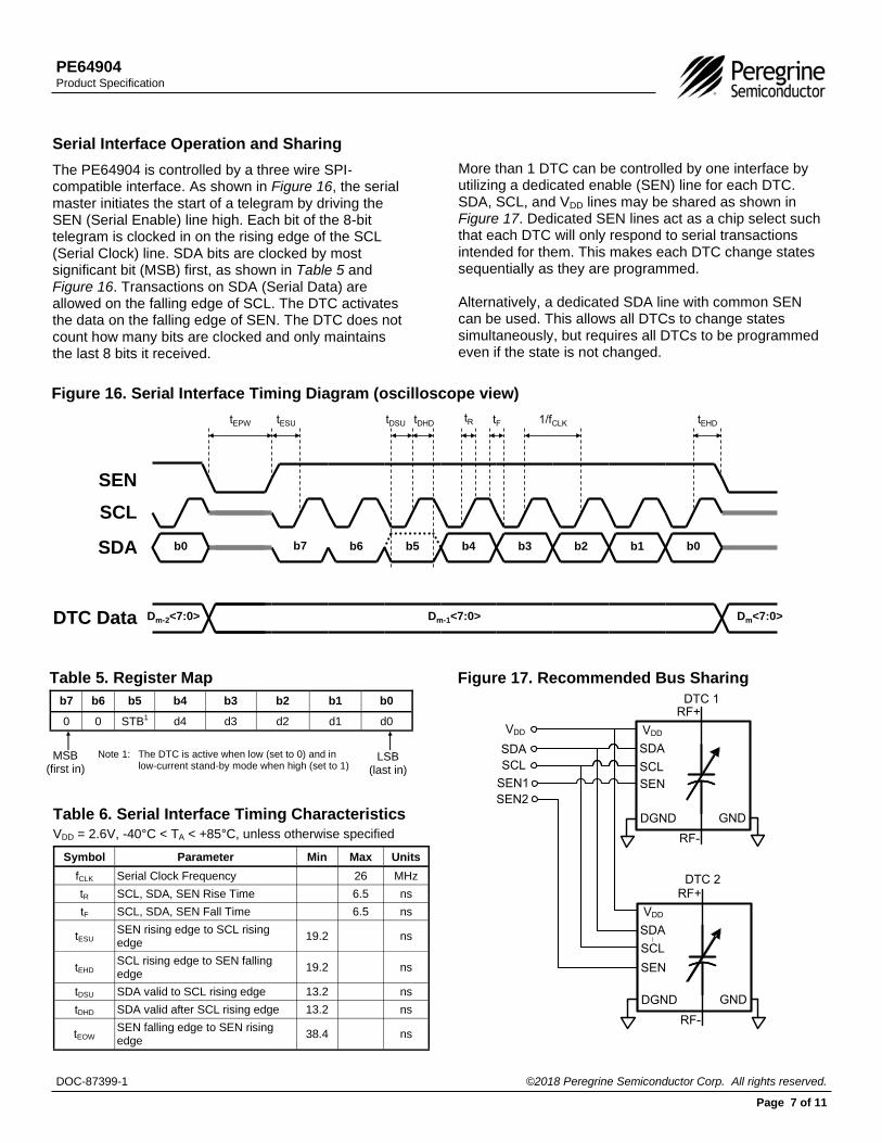
The PE64904 is controlled by a three wire SPI-compatible interface. As shown in Figure 16, the serial master initiates the start of a telegram by driving the SEN (Serial Enable) line high. Each bit of the 8-bit telegram is clocked in on the rising edge of the SCL (Serial Clock) line. SDA bits are clocked by most significant bit (MSB) first, as shown in Table 5 and Figure 16. Transactions on SDA (Serial Data) are allowed on the falling edge of SCL. The DTC activates the data on the falling edge of SEN. The DTC does not count how many bits are clocked and only maintains the last 8 bits it received.
Figure 17. Recommended Bus Sharing
SCL
SDA
VDD
GNDDGND
RF-
RF+
SCL
SDA
VDD
SEN
GNDDGND
RF-
RF+
SCL
SDA
VDD
DTC 1
SEN
SEN2
SEN1
DTC 2
More than 1 DTC can be controlled by one interface by utilizing a dedicated enable (SEN) line for each DTC. SDA, SCL, and VDD lines may be shared as shown in Figure 17. Dedicated SEN lines act as a chip select such that each DTC will only respond to serial transactions intended for them. This makes each DTC change states sequentially as they are programmed. Alternatively, a dedicated SDA line with common SEN can be used. This allows all DTCs to change states simultaneously, but requires all DTCs to be programmed even if the state is not changed.
Figure 16. Serial Interface Timing Diagram (oscilloscope view)
Note 1: The DTC is active when low (set to 0) and in low-current stand-by mode when high (set to 1)
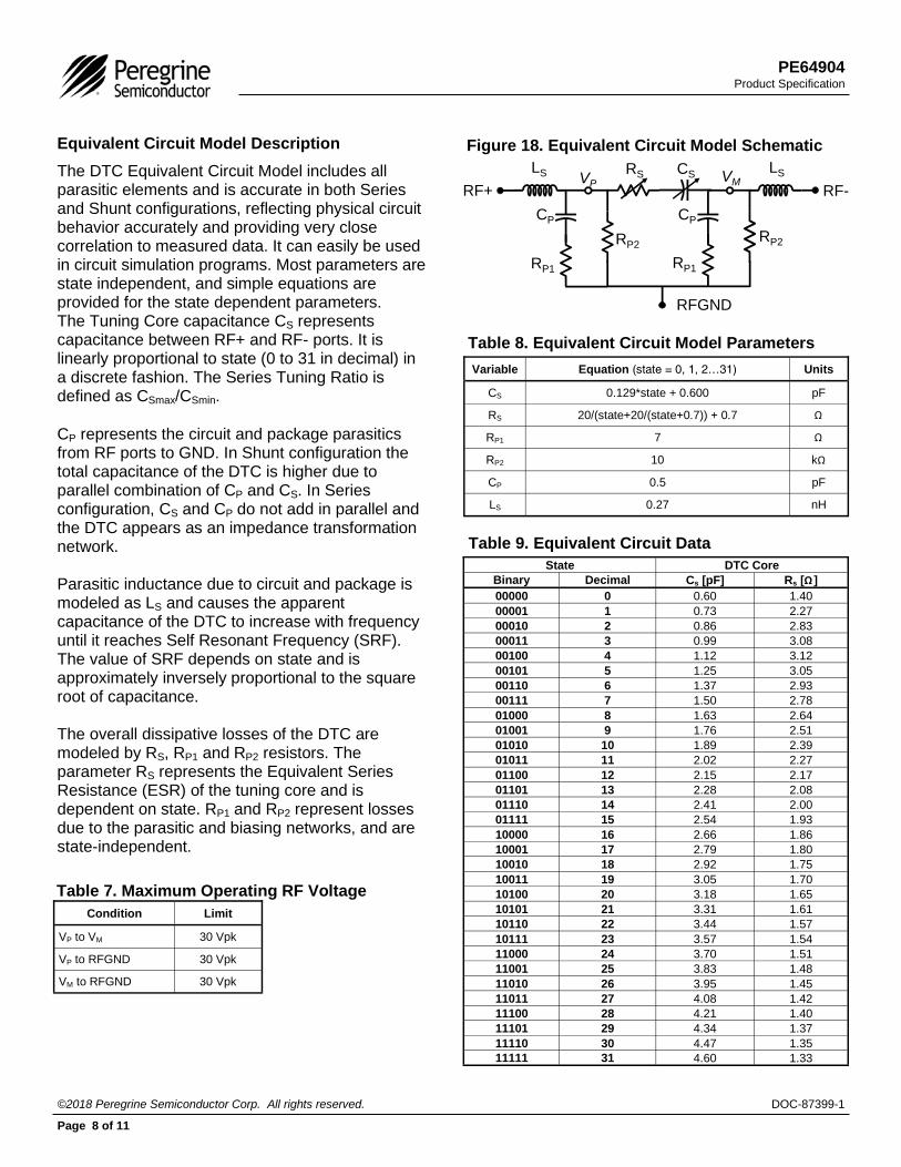
Figure 18. Equivalent Circuit Model Schematic Equivalent Circuit Model Description
The DTC Equivalent Circuit Model includes all parasitic elements and is accurate in both Series and Shunt configurations, reflecting physical circuit behavior accurately and providing very close correlation to measured data. It can easily be used in circuit simulation programs. Most parameters are state independent, and simple equations are provided for the state dependent parameters. The Tuning Core capacitance CS represents capacitance between RF+ and RF- ports. It is linearly proportional to state (0 to 31 in decimal) in a discrete fashion. The Series Tuning Ratio is defined as CSmax/CSmin.
CP represents the circuit and package parasitics from RF ports to GND. In Shunt configuration the total capacitance of the DTC is higher due to parallel combination of CP and CS. In Series configuration, CS and CP do not add in parallel and the DTC appears as an impedance transformation network. Parasitic inductance due to circuit and package is modeled as LS and causes the apparent capacitance of the DTC to increase with frequency until it reaches Self Resonant Frequency (SRF). The value of SRF depends on state and is approximately inversely proportional to the square root of capacitance. The overall dissipative losses of the DTC are modeled by RS, RP1 and RP2 resistors. The parameter RS represents the Equivalent Series Resistance (ESR) of the tuning core and is dependent on state. RP1 and RP2 represent losses due to the parasitic and biasing networks, and are state-independent.
For optimal results, place a ground fill directly under the DTC package on the PCB. Layout isolation is desired between all control and RF lines. When using the DTC in a shunt configuration, it is important to make sure the RF-pin is solidly grounded to a filled ground plane. Ground traces should be as short as possible to minimize inductance. A continuous ground plane is preferred on the top layer of the PCB. When multiple DTCs are used together, the physical distance between them should be minimized and the connection should be as wide as possible to minimize series parasitic inductance.
Evaluation Board
The 101-0597 Evaluation Board (EVB) was designed for accurate measurement of the DTC impedance and loss. Two configurations are available: 1 Port Shunt (J3) and 2 Port Series (J4, J5). Three calibration standards are provided. The open (J2) and short (J1) standards (104 ps delay) are used for performing port extensions and accounting for electrical length and transmission line loss. The Thru (J9, J10) standard can be used to estimate PCB transmission line losses for scalar de-embedding of the 2 Port Series configuration (J4, J5). The board consists of a 4 layer stack with 2 outer layers made of Rogers 4350B (εr = 3.48) and 2 inner layers of FR4 (εr = 4.80). The total thickness of this board is 62 mils (1.57 mm). The inner layers provide a ground plane for the transmission lines. Each transmission line is designed using a coplanar waveguide with ground plane (CPWG) model using a trace width of 32 mils (0.813 mm), gap of 15 mils (0.381 mm), and a metal thickness of 1.4 mils (0.051 mm).
For sales and contact information please visit www.psemi.com.
Advance Information: The product is in a formative or design stage. The datasheet contains design target specifications for product development. Specifications and features may change in any manner without notice. Preliminary Specification: The datasheet contains preliminary data. Additional data may be added at a later date. Peregrine reserves the right to change specifications at any time without notice in order to supply the best possible product. Product Specification: The datasheet contains final data. In the event Peregrine decides to change the specifications, Peregrine will notify customers of the intended changes by issuing a CNF (Customer Notification Form).
The information in this document is believed to be reliable. However, Peregrine assumes no liability for the use of this information. Use shall be entirely at the user’s own risk.