15
PCN IPG-PWR/14/8552 Dated 23 Jun 2014 DPAK Matrix Large Die Pad Back-End Capacity Extension - Nantong Fujitsu Microelectronics (China) 1/15 PRODUCT/PROCESS CHANGE NOTIFICATION ®

PCN IPG-PWR/14/8552Dated 23 Jun 2014
DPAK Matrix Large Die Pad Back-End Capacity Extension -
Nantong Fujitsu Microelectronics (China)
1/15
PRODUCT/PROCESSCHANGE NOTIFICATION®

PCN IPG-PWR/14/8552 - Dated 23 Jun 2014
Table 1. Change Implementation ScheduleForecasted implementation date for 16-Jun-2014 change
Forecasted availability date of samples 16-Jun-2014 for customer
Forecasted date for STMicroelectronicschange Qualification Plan results availability 16-Jun-2014
Estimated date of changed product first 22-Sep-2014 shipment
Table 2. Change IdentificationProduct Identification see attached list (Product Family/Commercial Product)
Type of change Package assembly process change
Reason for change Improve service to Customers
Description of the change Continuing in the aim of a constant process improvement, please beinformed that we’re going to use Automatic Assembly/Testing DPAKMatrix & Large Die Pad line for Selected Power BIPOLAR and PowerMOSFET Transistors produced in Nantong Fujitsu Microelectronics(China). You may already receive products in DPAK Matrix & Large DiePad line from Longgang or Shenzhen (China). DPAK device products,manufactured in Nantong Fujitsu Microelectronics (China), guaranteethe same quality and electrical characteristics as reported in therelevant data sheets. Devices used for qualification are available assamples.
Change Product Identification by data code.
Manufacturing Location(s)
® 2/15

PCN IPG-PWR/14/8552 - Dated 23 Jun 2014
Table 3. List of AttachmentsCustomer Part numbers list
Qualification Plan results
Qualification Plan Denied Name:
Qualification Plan Approved Title:
Customer Acknowledgement of Receipt PCN IPG-PWR/14/8552
Please sign and return to STMicroelectronics Sales Office Dated 23 Jun 2014
Company:
Change Denied Date:
Change Approved Signature:
Remark
.....................................................................................................................................................................................................
.....................................................................................................................................................................................................
.....................................................................................................................................................................................................
.....................................................................................................................................................................................................
.....................................................................................................................................................................................................
.....................................................................................................................................................................................................
.....................................................................................................................................................................................................
.....................................................................................................................................................................................................
® 3/15

PCN IPG-PWR/14/8552 - Dated 23 Jun 2014
DOCUMENT APPROVAL
Name Function
Mottese, Anna Marketing Manager
Aleo, Mario-Antonio Product Manager
Falcone, Giuseppe Q.A. Manager
® 4/15

1
Dear Customer,
Continuing in the aim of a constant process improvement, please be informed that we’re going to use
Automatic Assembly/Testing DPAK Matrix & Large Die Pad line for Selected Power BIPOLAR and Po-
wer MOSFET Transistors produced in Nantong Fujitsu Microelectronics (China). You may already receive
products in DPAK Matrix & Large Die Pad line from Longgang or Shenzhen (China). DPAK device pro-
ducts, manufactured in Nantong Fujitsu Microelectronics (China), guarantee the same quality and electrical
characteristics as reported in the relevant data sheets. Devices used for qualification are available as
samples.
The involved product series and affected packages are listed in the attached file.
Any other Product related to the above series, manufactured in Nantong Fujitsu Microelectronics (China),
even if not expressly included or partially mentioned in the attached table, is affected by this change.
Qualification program and results availability:
The reliability test report is provided in attachment to this document.
Samples availability:
Samples of the test vehicle devices will be available on request starting from week 23-2014.
Any other sample request will be processed and scheduled by Power Transistor Division upon request.
Product Family Description Package Part Number - Test Vehicle
Power MOSFET Transistors
Power BIPOLAR Transistors DPAK
STD5NK60ZT4
BUL742C
Change implementation schedule:
The production start and first shipments will be implemented according to our work in progress and
materials availability:
Product Family 1st Shipments
Power MOSFET Transistors
Power BIPOLAR Transistors From Week 36-2014
Lack of acknowledgement of the PCN within 30 days will constitute acceptance of the change. After
acknowledgement, lack of additional response within the 90 days period will constitute acceptance of the
change (Jedec Standard No. 46-C). In any case, first shipment may start earlier with customer written
agreement.

2
Marking and traceability:
Unless otherwise stated by customer specific requirement, traceability of Power BIPOLAR and Power
MOSFET Transistors produced in Nantong Fujitsu Microelectronics (China) will be ensured by the Q.A.
number marked on the package.
Sincerely Yours.

IPG (Industrial and Power Group) PTD (Power Transistor Division)
Quality and Reliability Rel 04-14
Page 1/8
Reliability Report DPAK Matrix Large Die Pad Back-End Capacity
Extension - Nantong Fujitsu Microelectronics (China)
General Information
Product Lines:
EZ63 – IV61
Product Families: Power MOSFET (EZ63) Power BIPOLAR (IV61)
P/Ns: STD5NK60ZT4 (EZ63) BULD742CT4 (IV61)
Product Group: IPG
Product division: Power Transistor Division
Package: DPAK
Silicon Process techn.: Zener-Protected SuperMESH™ MOSFET Power BIPOLAR
Locations Wafer Diffusion Plants:
Ang Mo Kio (Singapore)
EWS Plants:
Ang Mo Kio (Singapore)
Assembly and testing plant:
Nantong Fujitsu Microelectronics (NFME) (China)
Reliability Lab: IPG-PTD Catania Reliability Lab.
DOCUMENT INFORMATION
Version Date Pages Prepared by Approved by Comment 1.0 June 2014 8 A. Settinieri C. Cappello First issue
Note: This report is a summary of the reliability trials performed in good faith by STMicroelectronics in order to evaluate the potential reliability risks during the product life using a set of defined test methods. This report does not imply for STMicroelectronics expressly or implicitly any contractual obligations other than as set forth in STMicroelectronics general terms and conditions of Sale. This report and its contents shall not be disclosed to a third party without previous written agreement from STMicroelectronics.

IPG (Industrial and Power Group) PTD (Power Transistor Division)
Quality and Reliability Rel 04-14
Page 2/8
TABLE OF CONTENTS
1 APPLICABLE AND REFERENCE DOCUMENTS ............................................................................................3 2 GLOSSARY........................................................................................................................................................3 3 RELIABILITY EVALUATION OVERVIEW.........................................................................................................3
3.1 OBJECTIVES ...............................................................................................................................................3 3.2 CONCLUSION ..............................................................................................................................................3
4 DEVICE CHARACTERISTICS...........................................................................................................................4 4.1 DEVICE DESCRIPTION ..................................................................................................................................4 4.2 CONSTRUCTION NOTE .................................................................................................................................4
5 TESTS RESULTS SUMMARY...........................................................................................................................6 5.1 TEST VEHICLE.............................................................................................................................................6 5.2 RELIABILITY TEST PLAN SUMMARY ................................................................................................................6
6 ANNEXES 6.0.....................................................................................................................................................8 6.1TESTS DESCRIPTION ........................................................................................................................................8

IPG (Industrial and Power Group) PTD (Power Transistor Division)
Quality and Reliability Rel 04-14
Page 3/8
1 APPLICABLE AND REFERENCE DOCUMENTS
Document reference Short description JESD47 Stress-Test-Driven Qualification of Integrated Circuits
2 GLOSSARY DUT Device Under Test SS Sample Size HF Halogen Free
3 RELIABILITY EVALUATION OVERVIEW
3.1 Objectives Reliability evaluation for assembly and testing DPAK Matrix Large Die Pad Back-End Capacity Extension - Nantong Fujitsu Microelectronics (China)
3.2 Conclusion Qualification Plan requirements have been fulfilled without exception. It is stressed that reliability tests have shown that the devices behave correctly against environmental tests (no failure). Moreover, the stability of electrical parameters during the accelerated tests demonstrates the ruggedness of the products and safe operation, which is consequently expected during their lifetime.

IPG (Industrial and Power Group) PTD (Power Transistor Division)
Quality and Reliability Rel 04-14
Page 4/8
4 DEVICE CHARACTERISTICS
4.1 Device description N-channel Power MOSFET Power BIPOLAR
4.2 Construction note
D.U.T.: STD5NK60ZT4 LINE: EZ63 PACKAGE: DPAK
Wafer/Die fab. Information Wafer fab manufacturing location Ang Mo Kio (Singapore) Technology Zener-Protected SuperMESH™ MOSFET Die finishing back side Ti/Ni/Ag Die size 3900 x 2890 µm2 Metal Al/Si Passivation type Nitride
Wafer Testing (EWS) information
Electrical testing manufacturing location Ang Mo Kio (Singapore) Test program WPIS
Assembly information
Assembly site Nantong Fujitsu Microelectronics (NFME) Package description DPAK
Molding compound HF Epoxy Resin Frame material Raw Copper
Die attach process Soft Solder Die attach material Pb/Sn/Ag
Wire bonding process Ultrasonic Wires bonding materials Al/Mg Gate – Al Source Lead finishing/bump solder material Pure Tin
Final testing information
Testing location Nantong Fujitsu Microelectronics (NFME) Tester TESEC
IPG (Industrial and Power Group) PTD (Power Transistor Division)
Quality and Reliability Rel 04-14
Page 5/8
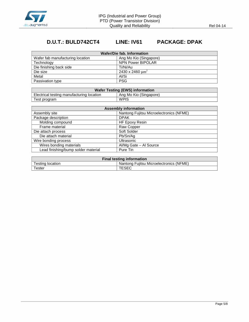
D.U.T.: BULD742CT4 LINE: IV61 PACKAGE: DPAK
Wafer/Die fab. Information
Wafer fab manufacturing location Ang Mo Kio (Singapore) Technology NPN Power BIPOLAR Die finishing back side Ti/Ni/Au Die size 2430 x 2460 µm2 Metal Al/Si Passivation type PSG
Wafer Testing (EWS) information
Electrical testing manufacturing location Ang Mo Kio (Singapore) Test program WPIS
Assembly information
Assembly site Nantong Fujitsu Microelectronics (NFME) Package description DPAK
Molding compound HF Epoxy Resin Frame material Raw Copper
Die attach process Soft Solder Die attach material Pb/Sn/Ag
Wire bonding process Ultrasonic Wires bonding materials Al/Mg Gate – Al Source Lead finishing/bump solder material Pure Tin
Final testing information
Testing location Nantong Fujitsu Microelectronics (NFME) Tester TESEC
IPG (Industrial and Power Group) PTD (Power Transistor Division)
Quality and Reliability Rel 04-14
Page 6/8
5 TESTS RESULTS SUMMARY
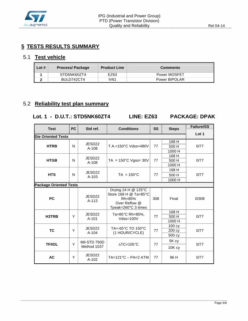
5.1 Test vehicle
Lot # Process/ Package Product Line Comments
1 STD5NK60ZT4 EZ63 Power MOSFET 2 BULD742CT4 IV61 Power BIPOLAR
5.2 Reliability test plan summary
Lot. 1 - D.U.T.: STD5NK60ZT4 LINE: EZ63 PACKAGE: DPAK
Failure/SS Test PC Std ref. Conditions SS Steps
Die Oriented Tests Lot 1
168 H 500 H HTRB N JESD22
A-108 T.A.=150°C Vdss=480V 77
1000 H 0/77
168 H 500 H HTGB N JESD22
A-108 TA = 150°C Vgss= 30V 77 1000 H
0/77
168 H 500 H HTS N JESD22
A-103 TA = 150°C 77 1000 H
0/77
Package Oriented Tests
PC JESD22 A-113
Drying 24 H @ 125°C Store 168 H @ Ta=85°C
Rh=85% Over Reflow @
Tpeak=260°C 3 times
308 Final 0/308
168 H 500 H H3TRB Y JESD22
A-101 Ta=85°C Rh=85%,
Vdss=100V 77 1000 H
0/77
100 cy 200 cy TC Y JESD22
A-104 TA=-65°C TO 150°C (1 HOUR/CYCLE) 77
500 cy 0/77
5K cy TF/IOL Y Mil-STD 750D
Method 1037 ∆TC=105°C 77 10K cy
0/77
AC Y JESD22 A-102 TA=121°C – PA=2 ATM 77 96 H 0/77

IPG (Industrial and Power Group) PTD (Power Transistor Division)
Quality and Reliability Rel 04-14
Page 7/8
Lot. 2 - D.U.T.: BULD742CT4 LINE: IV61 PACKAGE: DPAK
Failure/SS Test PC Std ref. Conditions SS Steps
Die Oriented Tests Lot 2
168 H 500 H HTRB N
JESD22 A-108 T.A.=150°C Vdss=480V 77
1000 H 0/77
168 H 500 H HTS N JESD22
A-103 TA = 150°C 77 1000 H
0/77
Package Oriented Tests
PC JESD22 A-113
Drying 24 H @ 125°C Store 168 H @ Ta=85°C
Rh=85% Over Reflow @
Tpeak=260°C 3 times
308 Final 0/308
168 H 500 H H3TRB Y JESD22
A-101 Ta=85°C Rh=85%,
Vdss=100V 77 1000 H
0/77
100 cy 200 cy TC Y JESD22
A-104 TA=-65°C TO 150°C (1 HOUR/CYCLE)
77 500 cy
0/77
5K cy TF/IOL Y Mil-STD 750D
Method 1037 ∆TC=105°C 77 10K cy
0/77
AC Y JESD22 A-102 TA=121°C – PA=2 ATM 77 96 H 0/77

IPG (Industrial and Power Group) PTD (Power Transistor Division)
Quality and Reliability Rel 04-14
Page 8/8
6 ANNEXES 6.0
6.1Tests Description
Test name Description Purpose
Die Oriented Tests
HTRB High Temperature
Reverse Bias
HTGB High Temperature
Forward (Gate) Bias
The device is stressed in static configuration, trying to satisfy as much as possible the following conditions: • low power dissipation; • max. supply voltage compatible with
diffusion process and internal circuitry limitations;
To determine the effects of bias conditions and temperature on solid state devices over time. It simulates the devices’ operating condition in an accelerated way. To maximize the electrical field across either reverse-biased junctions or dielectric layers, in order to investigate the failure modes linked to mobile contamination, oxide ageing, layout sensitivity to surface effects.
HTSL High Temperature
Storage Life
The device is stored in unbiased condition at the max. temperature allowed by the package materials, sometimes higher than the max. operative temperature.
To investigate the failure mechanisms activated by high temperature, typically wire-bonds solder joint ageing, data retention faults, metal stress-voiding.
Package Oriented Tests AC
Auto Clave (Pressure Pot)
The device is stored in saturated steam, at fixed and controlled conditions of pressure and temperature.
To investigate corrosion phenomena affecting die or package materials, related to chemical contamination and package hermeticity.
TC Temperature
Cycling
The device is submitted to cycled temperature excursions, between a hot and a cold chamber in air atmosphere.
To investigate failure modes related to the thermo-mechanical stress induced by the different thermal expansion of the materials interacting in the die-package system. Typical failure modes are linked to metal displacement, dielectric cracking, molding compound delamination, wire-bonds failure, die-attach layer degradation.
TF / IOL Thermal Fatigue /
Intermittent Operating Life
The device is submitted to cycled temperature excursions generated by power cycles (ON/OFF) at T ambient.
To investigate failure modes related to the thermo-mechanical stress induced by the different thermal expansion of the materials interacting in the die-package system. Typical failure modes are linked to metal displacement, dielectric cracking, molding compound delamination, wire-bonds failure, die-attach layer degradation.
H3TRB Temperature Humidity Bias
The device is biased in static configuration minimizing its internal power dissipation, and stored at controlled conditions of ambient temperature and relative humidity.
To evaluate the package moisture resistance with electrical field applied, both electrolytic and galvanic corrosion are put in evidence.

PCN IPG-PWR/14/8552 - Dated 23 Jun 2014
Please Read Carefully:
Information in this document is provided solely in connection with ST products. STMicroelectronics NV and its subsidiaries(‘‘ST’’) reserve theright to make changes, corrections, modifications or improvements, to this document, and the products and services described herein at anytime, without notice.
All ST products are sold pursuant to ST’s terms and conditions of sale.
Purchasers are solely responsible for the choice, selection and use of the ST products and services described herein, and ST assumes noliability whatsoever relating to the choice, selection or use of the ST products and services described herein.
No license, express or implied, by estoppel or otherwise, to any intellectual property rights is granted under this document. If any part of thisdocument refers to any third party products or services it shall not be deemed a license grant by ST for the use of such third party productsor services, or any intellectual property contained therein or considered as a warranty covering the use in any manner whatsoever of suchthird party products or services or any intellectual property contained therein.
UNLESS OTHERWISE SET FORTH IN ST’S TERMS AND CONDITIONS OF SALE ST DISCLAIMS ANY EXPRESS OR IMPLIEDWARRANTY WITH RESPECT TO THE USE AND / OR SALE OF ST PRODUCTS INCLUDING WITHOUT LIMITATION IMPLIEDWARRANTIES OF MERCHANTABILITY, FITNESS FOR A PARTICULAR PURPOSE ( AND THEIR EQUIVALENTS UNDER THE LAWSOF ANY JURISDICTION ), OR INFRINGEMENT OF ANY PATENT, COPYRIGHT OR OTHER INTELLECTUAL PROPERTY RIGHT.
ST PRODUCTS ARE NOT DESIGNED OR AUTHORIZED FOR USE IN: (A) SAFETY CRITICAL APPLICATIONS SUCH AS LIFESUPPORTING, ACTIVE IMPLANTED DEVICES OR SYSTEMS WITH PRODUCT FUNCTIONAL SAFETY REQUIREMENTS;(B) AERONAUTIC APPLICATIONS; (C) AUTOMOTIVE APPLICATIONS OR ENVIRONMENTS, AND/OR (D) AEROSPACEAPPLICATIONS OR ENVIRONMENTS. WHERE ST PRODUCTS ARE NOT DESIGNED FOR SUCH USE, THE PURCHASER SHALLUSE PRODUCTS AT PURCHASER’S SOLE RISK, EVEN IF ST HAS BEEN INFORMED IN WRITING OF SUCH USAGE, UNLESS APRODUCT IS EXPRESSLY DESIGNATED BY ST AS BEING INTENDED FOR ‘‘AUTOMOTIVE, AUTOMOTIVE SAFETY OR MEDICAL’’INDUSTRY DOMAINS ACCORDING TO ST PRODUCT DESIGN SPECIFICATIONS. PRODUCTS FORMALLY ESCC, QML ORJAN QUALIFIED ARE DEEMED SUITABLE FOR USE IN AEROSPACE BY THE CORRESPONDING GOVERNMENTAL AGENCY.
RESTRICTIONS OF USE AND CONFIDENTIALITY OBLIGATIONS:
THIS DOCUMENT AND ITS ANNEXES CONTAIN ST PROPRIETARY AND CONFIDENTIAL INFORMATION. THE DISCLOSURE,DISTRIBUTION, PUBLICATION OF WHATSOEVER NATURE OR USE FOR ANY OTHER PURPOSE THAN PROVIDED IN THISDOCUMENT OF ANY INFORMATION CONTAINED IN THIS DOCUMENT AND ITS ANNEXES IS SUBMITTED TO ST PRIOR EXPRESS AUTHORIZATION. ANY UNAUTHORIZED REVIEW, USE, DISCLOSURE OR DISTRIBUTION OF SUCH INFORMATION ISEXPRESSLY PROHIBITED.
Resale of ST products with provisions different from the statements and/or technical features set forth in this document shall immediately voidany warranty granted by ST for the ST product or service described herein and shall not create or extend in any manner whatsoever, anyliability of ST.
ST and the ST logo are trademarks or registered trademarks of ST in various countries.
Information in this document supersedes and replaces all information previously supplied.
The ST logo is a registered trademark of STMicroelectronics. All other names are the property of their respective owners
c 2014 STMicroelectronics - All rights reserved.
STMicroelectronics group of companies
Australia - Belgium - Brazil - Canada - China - Czech Republic - Finland - France - Germany - Hong Kong - India - Israel - Italy - Japan -
Malaysia - Malta - Morocco - Philippines - Singapore - Spain - Sweden - Switzerland - United Kingdom - United States of America
www.st.com
® 15/15


