P.Ravindran, PHY02E – Semiconductor Physics, Autum 2013 17 December : Introduction to Semiconductors http://folk.uio.no/ravi/semi2013 Prof.P. Ravindran, Department of Physics, Central University of Tamil Nadu, India Carrier Mobility and Hall Effect 1
Transcript
P.Ravindran, PHY02E – Semiconductor Physics, Autum 2013 17 December : Introduction to Semiconductors
http://folk.uio.no/ravi/semi2013
Prof.P. Ravindran, Department of Physics, Central University of Tamil
Nadu, India
Carrier Mobility and Hall Effect
1
P.Ravindran, PHY02E – Semiconductor Physics, Autum 2013 17 December : Introduction to Semiconductors
calculation
Calculate the hole and electron densities in a piece of p-type silicon
that has been doped with 5 x 10¹⁶ acceptor atoms per cm3 .
ni = 1.4 x 1010 cm-3 ( at room temperature)
Undoped
n = p = ni
p-type ; p >> n
n.p = ni2 NA = 5 x 10¹⁶ p = NA = 5 x 1016 cm-3
3
316
23102
109.3105
)104.1(x
cmx
cmx
p
nn i
electrons per cm3
p >> ni and n << ni in a p-type material. The more holes you put in the less e-’s you have and vice versa.
P.Ravindran, PHY02E – Semiconductor Physics, Autum 2013 17 December : Introduction to Semiconductors3
Diffusion current
Reasons:
– concentration difference
(gradient)
– thermal movement
Proportional to the gradient
D: diffusion constant [m2/s]
nDqJ nn grad
pDqJ pp grad
P.Ravindran, PHY02E – Semiconductor Physics, Autum 2013 17 December : Introduction to Semiconductors
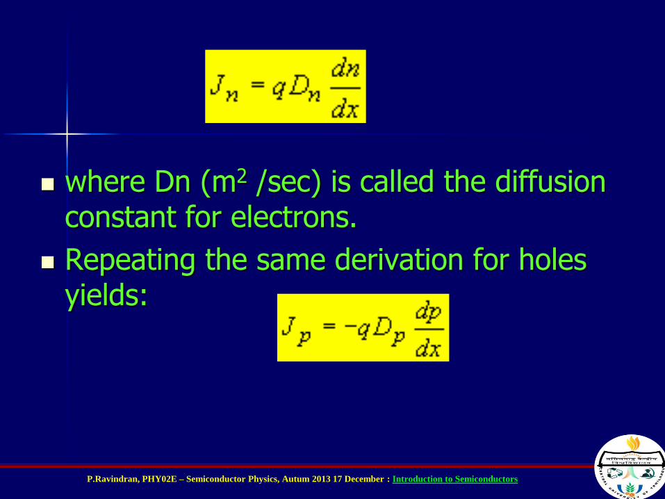
where Dn (m2 /sec) is called the diffusion constant for electrons.
Repeating the same derivation for holes yields:
P.Ravindran, PHY02E – Semiconductor Physics, Autum 2013 17 December : Introduction to Semiconductors
Total Current
It is possible for both a potential gradient and a concentration gradient to exist simultaneously within a semiconductor. In such a situation the total electron current density is:
And
The total current )( pntotal JJAI
P.Ravindran, PHY02E – Semiconductor Physics, Autum 2013 17 December : Introduction to Semiconductors6
Total currents
nDqEqnJ nnn grad
pDqEpqJ ppp grad
q
kTD Einstein's relationship
mV26V026.0[As]106.1
[K]300[VAs/K]1038.119
23
300
KT
Tq
kTU
Thermal voltage
P.Ravindran, PHY02E – Semiconductor Physics, Autum 2013 17 December : Introduction to Semiconductors
The Einstein Relationship
Since both diffusion and mobility are statistical thermodynamic phenomena, D and μ are not independent. The relationship between them is given by the Einstein equation
where VT is the "volt equivalent of temperature” defined by
where k is the Boltzmann constant in joules per Kelvin.
T
n
n
p
pV
DD
VT
q
TkVT
11600
P.Ravindran, PHY02E – Semiconductor Physics, Autum 2013 17 December : Introduction to Semiconductors
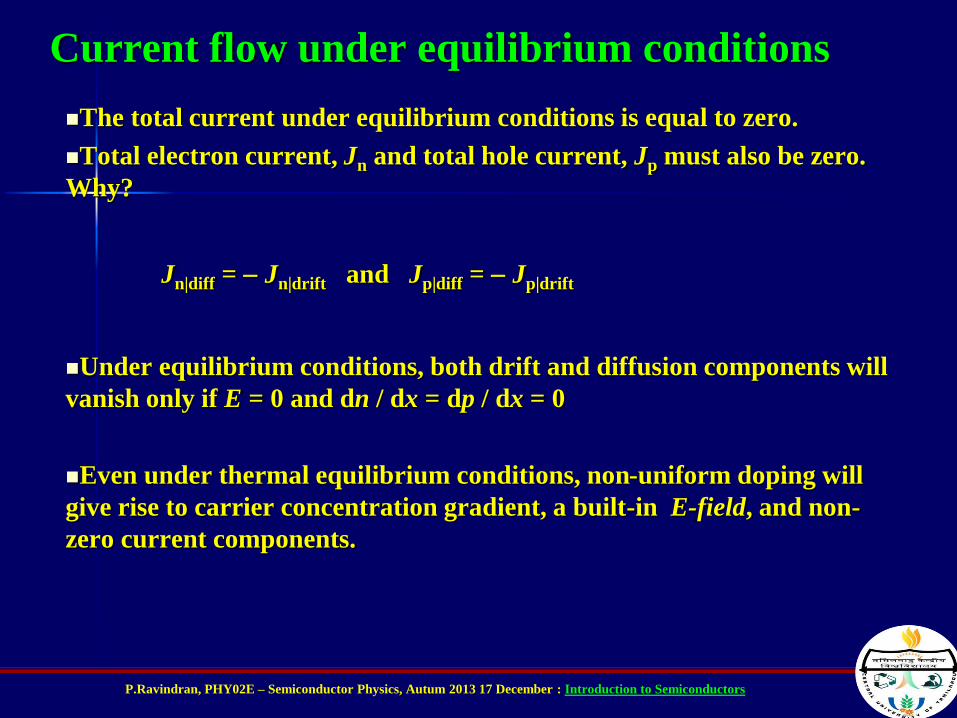
Current flow under equilibrium conditions
The total current under equilibrium conditions is equal to zero.
Total electron current, Jn and total hole current, Jp must also be zero.
Why?
Jn|diff = Jn|drift and Jp|diff = Jp|drift
Under equilibrium conditions, both drift and diffusion components will
vanish only if E = 0 and dn / dx = dp / dx = 0
Even under thermal equilibrium conditions, non-uniform doping will
give rise to carrier concentration gradient, a built-in E-field, and non-
zero current components.
P.Ravindran, PHY02E – Semiconductor Physics, Autum 2013 17 December : Introduction to Semiconductors
Under equilibrium conditions, dEF / dx = 0; the Fermi
level inside a material or a group of materials in intimate
contact is invariant as a function of position.
–EF appears as a horizontal line on equilibrium energy
band diagram.
–If the Fermi level is not constant with position, charge
transfer will take place resulting in a net current flow, in
contrast to the assumption of equilibrium conditions.
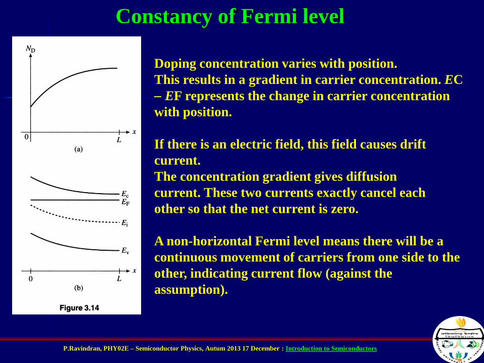
Constancy of Fermi level
P.Ravindran, PHY02E – Semiconductor Physics, Autum 2013 17 December : Introduction to Semiconductors10
Constancy of Fermi level
Doping concentration varies with position.
This results in a gradient in carrier concentration. EC
EF represents the change in carrier concentration
with position.
If there is an electric field, this field causes drift
current.
The concentration gradient gives diffusion
current. These two currents exactly cancel each
other so that the net current is zero.
A non-horizontal Fermi level means there will be a
continuous movement of carriers from one side to the
other, indicating current flow (against the
assumption).
P.Ravindran, PHY02E – Semiconductor Physics, Autum 2013 17 December : Introduction to Semiconductors
EXAMPLE: Given p = 470 cm2/V·s, what is the hole drift
velocity at E = 103 V/cm? What is tmp and what is the distance
traveled between collisions (called the mean free path) if the hole
velocity is 2.2107 cm/s? Hint: When in doubt, use the MKS
system of units.
Solution: n = pE = 470 cm2/V·s 103 V/cm = 4.7 105 cm/s
tmp = pmp/q =470 cm2/V ·s 0.39 9.110-31 kg/1.610-19 C
= 0.047 m2/V ·s 2.210-12 kg/C = 110-13s = 0.1 ps
mean free path = tmhnth ~ 1 10-13 s 2.2107 cm/s
= 2.210-6 cm = 220 Å = 22 nm
This is smaller than the typical dimensions of devices, but getting close.
Drift Velocity, Mean Free Time, Mean Free Path
P.Ravindran, PHY02E – Semiconductor Physics, Autum 2013 17 December : Introduction to SemiconductorsFrom Principles of Electronic Materials and
L = lattice vibration scattering limited mobility, T = temperature
L T3 / 2
Ionized Impurity Scattering Limited Mobility
I = ionized impurity scattering limited mobility, NI = concentration of the ionized
impurities (all ionized impurities including donors and acceptors)
I
IN
T 2/3
P.Ravindran, PHY02E – Semiconductor Physics, Autum 2013 17 December : Introduction to Semiconductors
Effective or Overall Mobility
e = effective drift mobility
I = ionized impurity scattering limited mobility
L = lattice vibration scattering limited mobility
1
e1
I
1
L
P.Ravindran, PHY02E – Semiconductor Physics, Autum 2013 17 December : Introduction to Semiconductors
Log-log plot of drift mobility versus temperature for n-type Ge and n-type Si samples.
Various donor concentrations for Si are shown. Nd are in cm-3. The upper right inset is
the simple theory for lattice limited mobility, whereas the lower left inset is the simple
theory for impurity scattering limited mobility.
P.Ravindran, PHY02E – Semiconductor Physics, Autum 2013 17 December : Introduction to Semiconductors
Drift mobility of Si at Τ= 300 K for various dopant concentration.
P.Ravindran, PHY02E – Semiconductor Physics, Autum 2013 17 December : Introduction to Semiconductors
Conductivity (σ), resistivity(ρ) , mobility (µ) and number of carrier (n)
with temperature in semiconductors.
P.Ravindran, PHY02E – Semiconductor Physics, Autum 2013 17 December : Introduction to Semiconductors
When we add carriers by doping, the number of additional carrers, Nd, far exceeds those in an intrinsic semiconductor, and we can treat conductivity as
s = 1/r = qdNd
Resistivity as a function of
charge mobility and number
carrier.
P.Ravindran, PHY02E – Semiconductor Physics, Autum 2013 17 December : Introduction to Semiconductors
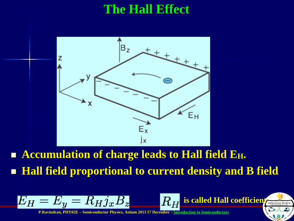
The Hall Effect
This phenomenon, discovered in 1879 by
American physics graduate student (!) Edwin
Hall, is important because it allows us to
measure the free-electron concentration n for
metals (and semiconductors!) and compare
to predictions of the FEG model.
The Hall effect is quite simple to
understand. Consider a B field applied
transverse to a thin metal sample carrying
a current:
I
P.Ravindran, PHY02E – Semiconductor Physics, Autum 2013 17 December : Introduction to Semiconductors
Hall effect
Hall effect was discovered in 1879 by Edward H. Hall
Exists in all conducting materials
It is particularly pronounced and useful in semiconductors.
Hall effect sensor is one of the simplest of all magnetic sensing devices
Used extensively in sensing position and measuring magnetic fields
P.Ravindran, PHY02E – Semiconductor Physics, Autum 2013 17 December : Introduction to Semiconductors
Hall effect
When a magnetic field is applied perpendicular to a current carrying
conductor or semiconductor, voltage is developed across the
specimen in a direction perpendicular to both the current and the
magnetic field. This phenomenon is called the Hall effect and voltage
so developed is called the Hall voltage.
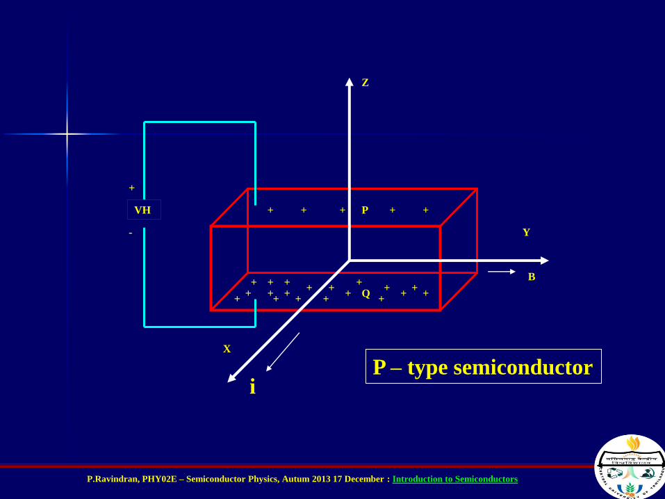
Let us consider, a thin rectangular slab carrying current (i) in the x-
direction.
If we place it in a magnetic field B which is in the y-direction.
Potential difference Vpq will develop between the faces p and q which
are perpendicular to the z-direction.
P.Ravindran, PHY02E – Semiconductor Physics, Autum 2013 17 December : Introduction to Semiconductors
i
B
P
Q
X
Y
Z
+ + ++ +VH
+++
++++
+ ++
++
+++
++ ++
+
-
P – type semiconductor
P.Ravindran, PHY02E – Semiconductor Physics, Autum 2013 17 December : Introduction to Semiconductors
i
B
X
Y
Z
VH
+
-
__
__
__
_
__
__
__
_
_
_
_ _ P
Q
N – type semiconductor
P.Ravindran, PHY02E – Semiconductor Physics, Autum 2013 17 December : Introduction to Semiconductors
Hall Effect in p & n-type semiconductors
Hall effect sign conventions for p-
type sample Hall effect sign conventions
for n-type sample
P.Ravindran, PHY02E – Semiconductor Physics, Autum 2013 17 December : Introduction to Semiconductors
Hall Effect Measurements
A hypothetical charge carrier of charge
q experiences a Lorentz force in the
lateral direction:
It
w
qvBFB
As more and more carriers are
deflected, the accumulation of charge
produces a “Hall field” EH that imparts
a force opposite to the Lorentz force:
HE qEF
Equilibrium is reached when these two
opposing forces are equal in magnitude,
which allows us to determine the drift
speed:
HqEqvBB
Ev H
From this we can write the current density:B
nqEnqvJ H
And it is customary to define the Hall
coefficient in terms of the measured
quantities:
nqJB
ER H
H
1
P.Ravindran, PHY02E – Semiconductor Physics, Autum 2013 17 December : Introduction to Semiconductors
Hall Effect Results!
In the lab we actually measure the Hall voltage VH and the current I, which gives
us a more useful way to write RH:
If we calculate RH from our
measurements and assume |q| = e
(which Hall did not know!) we can find
n. Also, the sign of VH and thus RH tells
us the sign of q!
nqIB
tV
BwtI
wV
JB
ER HHH
H
1
/
/wEV HH JwtJAI
RH (10-11 m3/As)
Metal n0 solid liquid FEG value
Na 1 -25 -25.5 -25.5
Cu 1 -5.5 -8.25 -8.25
Ag 1 -9.0 -12.0 -12.0
Au 1 -7.2 -11.8 -11.8
Be 2 +24.4 -2.6 -2.53
Zn 2 +3.3 -5 -5.1
Al 3 -3.5 -3.9 -3.9
The discrepancies between the FEG
predictions and expt. nearly vanish
when liquid metals are compared. This
reveals clearly that the source of these
discrepancies lies in the electron-lattice
interaction. But the results for Be and
Zn are puzzling. How can we have q >
0 ???
*
*
Stay tuned…..
P.Ravindran, PHY02E – Semiconductor Physics, Autum 2013 17 December : Introduction to Semiconductors
Hall Effect
0yj →
0y c x
q qE v
m q
t t
x x
qv E
m
t
0z z
qv E
m
t
y c x
qE E
q t
x
qBE
mct
Hall coefficient:
y
H
x
ER
j B
2
x
x
qBE
mc
nqE B
m
t
t
1
nqc
electrons
P.Ravindran, PHY02E – Semiconductor Physics, Autum 2013 17 December : Introduction to Semiconductors
P.Ravindran, PHY02E – Semiconductor Physics, Autum 2013 17 December : Introduction to Semiconductors
The Hall Effect
Accumulation of charge leads to Hall field EH.
Hall field proportional to current density and B field
is called Hall coefficient
P.Ravindran, PHY02E – Semiconductor Physics, Autum 2013 17 December : Introduction to Semiconductors
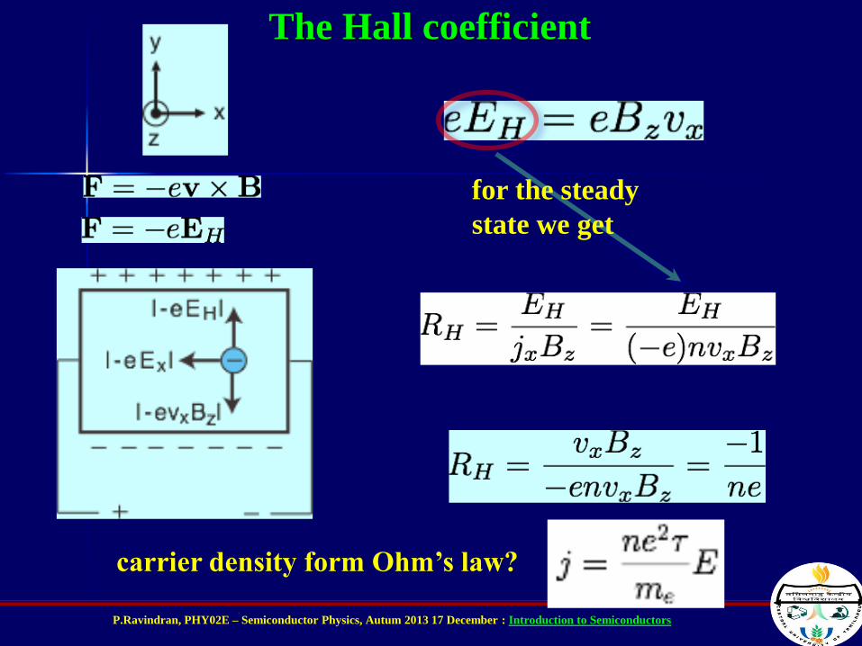
The Hall coefficient
carrier density form Ohm’s law?
for the steady
state we get
P.Ravindran, PHY02E – Semiconductor Physics, Autum 2013 17 December : Introduction to Semiconductors
The Hall coefficientOhm’s law contains e
2
But for RH the sign of e
is important.
P.Ravindran, PHY02E – Semiconductor Physics, Autum 2013 17 December : Introduction to Semiconductors
What would happen for positively charged carriers?
P.Ravindran, PHY02E – Semiconductor Physics, Autum 2013 17 December : Introduction to Semiconductors
Hall effect and magnetoresistance
Edwin Herbert Hall (1879): discovery of the Hall effect
HvF c
eL
the Lorentz force
in equilibrium jy = 0 → the transverse field (the Hall field) Ey due to the accumulated charges
balances the Lorentz force
quantities of interest:
magnetoresistance (transverse magnetoresistance)
Hall (off-diagonal) resistance
( ) xxx
x
y
yx
x
y
H
x
EH
j
E
j
ER
j H
r r
r
RH → measurement of the sign of the carrier charge
RH is positive for positive charges and negative for negative charges
the Hall effect is the electric
field developed across two
faces of a conductor
in the direction j×H
when a current j flows across
a magnetic field H
( ) xxx
x
y
yx
x
VR H R
I
VR
I
resistivity
Hall resistivity
the Hall coefficient
P.Ravindran, PHY02E – Semiconductor Physics, Autum 2013 17 December : Introduction to Semiconductors
mc
eH
ppeE
ppeE
mce
dt
d
ce
c
y
xcy
xycx
t
t
t
0
0
1
1
pHpE
p
HvEfforce acting on electron
equation of motion
for the momentum per electron
in the steady state px and py
satisfy
cyclotron frequency
frequency of revolution
of a free electron in the
magnetic field H
at H = 0.1 T
0yj xxc
y jnec
HjE
0s
t
multiply by
yxcy
xycx
jjE
jjE
ts
ts
0
0
m
ne
m
pnej
mne
ts
t
2
0
/
the Drude
model DC
conductivity
at H=0
Hrc
erm cc
2
weak magnetic fields – electrons can complete only a small part of revolution between collisions
strong magnetic fields – electrons can complete many revolutions between collisions1
1
t
t
c
c
1tcj is at a small angle f to E f is the Hall angle tan f ct
RH → measurement of the density
necRH
1xx Ej 0s
the resistance does not
depend on H
GHzcc 1~
2
n
P.Ravindran, PHY02E – Semiconductor Physics, Autum 2013 17 December : Introduction to Semiconductors
P.Ravindran, PHY02E – Semiconductor Physics, Autum 2013 17 December : Introduction to Semiconductors
P.Ravindran, PHY02E – Semiconductor Physics, Autum 2013 17 December : Introduction to Semiconductors
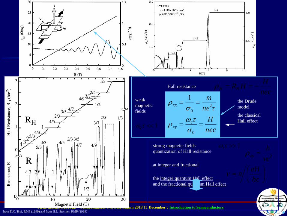
measurable quantity – Hall resistance HRHH r
ecn
H
I
V
Dx
y
H
2
r zD nLn 2for 3D systems
for 2D systems n2D=n
jE r Ej sin the presence of magnetic field the
resistivity and conductivity becomes tensors
yxcy
xycx
jjE
jjE
ts
ts
0
0
yyyx
xyxx
rr
rrr
0 0
0 0
1
1
cx x y
cy x y
E j j
E j j
t
s s
t
s s
for 2D:
00
00
1
1
sst
stsr
c
c
nec
H
ne
m
cxy
xx
0
2
0
1
s
tr
tsr
22
22
xyxx
xy
xy
xyxx
xxxx
rr
rs
rr
rs
2
0
2
0
)(1
)(1
t
tsss
t
sss
c
cyxxy
c
yyxx
1
yyyx
xyxx
yyyx
xyxx
rr
rr
ss
sss
x xx xy x
y yx yy y
E j
E j
r r
r r
0 0
0 0
1
1
x xc
y yc
E j
E j
s t s
t s s
x xx xy x
y yx yy y
j E
j E
s s
s s
P.Ravindran, PHY02E – Semiconductor Physics, Autum 2013 17 December : Introduction to Semiconductorsfrom D.C. Tsui, RMP (1999) and from H.L. Stormer, RMP (1999)