P.Ravindran, Nanomaterials and Nanotechnology, Spring 2016 1D Nanostructure – Nanowires/rods etc. . http://folk.uio.no/ravi/cutn/NMNT Prof.P. Ravindran, Department of Physics, Central University of Tamil Nadu, India & Center for Materials Science and Nanotechnology, University of Oslo, Norway 1D Nanostructure – Nanowires/rods etc. 1
Transcript
P.Ravindran, Nanomaterials and Nanotechnology, Spring 2016 1D Nanostructure – Nanowires/rods etc.
.
http://folk.uio.no/ravi/cutn/NMNT
Prof.P. Ravindran, Department of Physics, Central University of Tamil
Nadu, India
&Center for Materials Science and Nanotechnology,
University of Oslo, Norway
1D Nanostructure – Nanowires/rods etc.
1
P.Ravindran, Nanomaterials and Nanotechnology, Spring 2016 1D Nanostructure – Nanowires/rods etc.
.
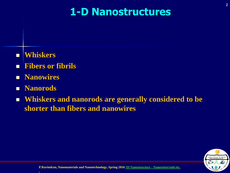
1-D Nanostructures
Whiskers
Fibers or fibrils
Nanowires
Nanorods
Whiskers and nanorods are generally considered to be
shorter than fibers and nanowires
2
P.Ravindran, Nanomaterials and Nanotechnology, Spring 2016 1D Nanostructure – Nanowires/rods etc.
.
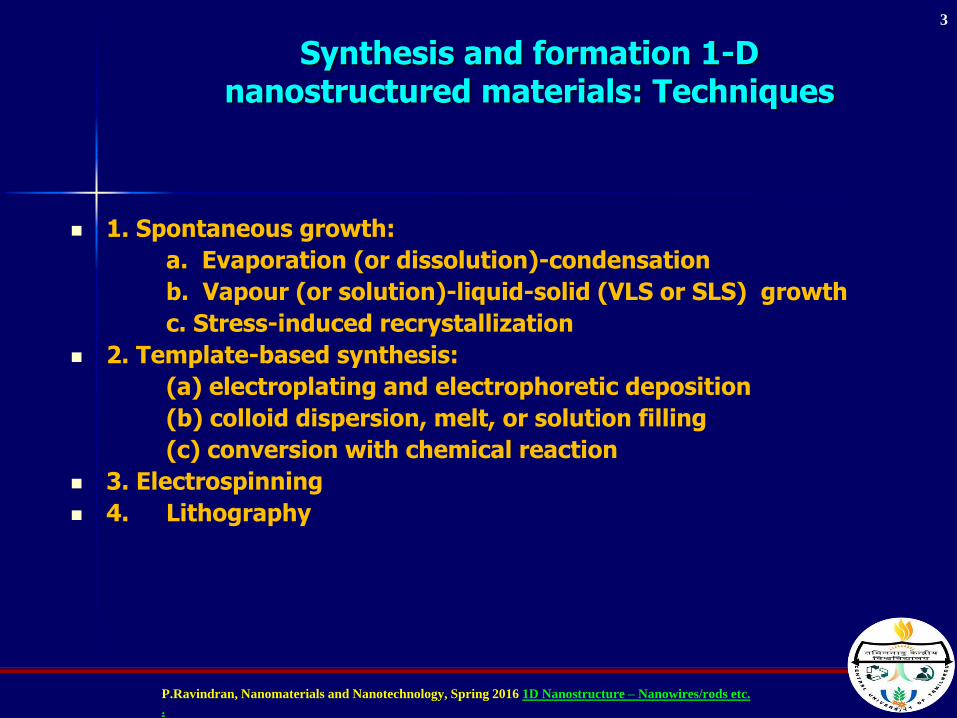
Synthesis and formation 1-D nanostructured materials: Techniques
1. Spontaneous growth:
a. Evaporation (or dissolution)-condensation
b. Vapour (or solution)-liquid-solid (VLS or SLS) growth
c. Stress-induced recrystallization
2. Template-based synthesis:
(a) electroplating and electrophoretic deposition
(b) colloid dispersion, melt, or solution filling
(c) conversion with chemical reaction
3. Electrospinning
4. Lithography
3
P.Ravindran, Nanomaterials and Nanotechnology, Spring 2016 1D Nanostructure – Nanowires/rods etc.
.
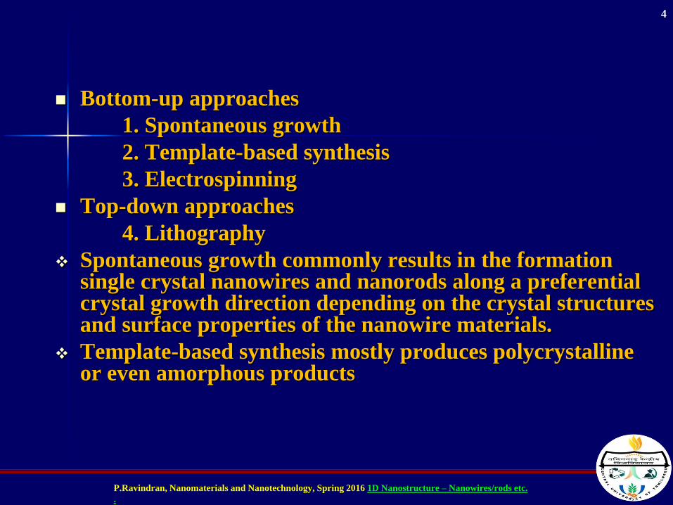
Bottom-up approaches
1. Spontaneous growth
2. Template-based synthesis
3. Electrospinning
Top-down approaches
4. Lithography
Spontaneous growth commonly results in the formation single crystal nanowires and nanorods along a preferential crystal growth direction depending on the crystal structures and surface properties of the nanowire materials.
Template-based synthesis mostly produces polycrystalline or even amorphous products
4
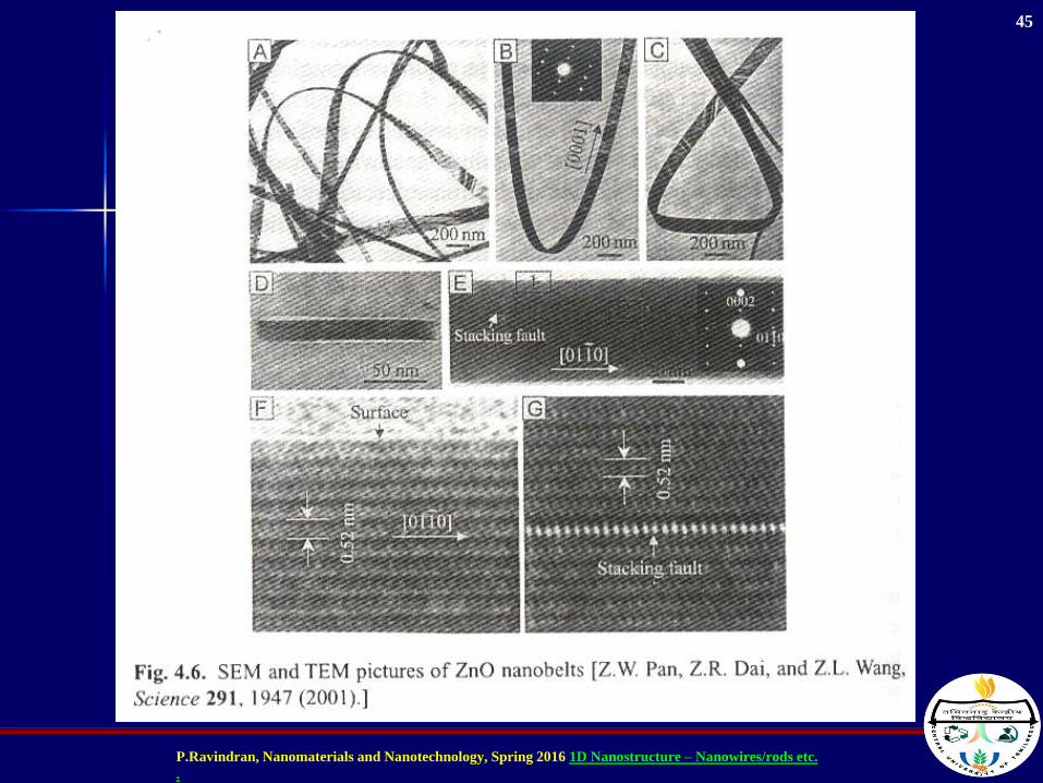
P.Ravindran, Nanomaterials and Nanotechnology, Spring 2016 1D Nanostructure – Nanowires/rods etc.
.
Spontaneous growth
Spontaneous growth is a process driven by the reduction of Gibbs free energy or chemical potential.
the reduction of Gibbs free energy is commonly realized by phase transformation or chemical reaction or the release of stress
For formation of nanowires or nanorods, anisotropic growth is required, i.e. the crystal grows along a certain orientation faster than other directions
Uniformly sized nanowires, i.e. the same diameter along the longitudinal direction of a given nanowire, can be obtained when crystal growth proceeds along one direction, whereas no growth along other directions
Morphology of final product affected by defects and impurities
5
P.Ravindran, Nanomaterials and Nanotechnology, Spring 2016 1D Nanostructure – Nanowires/rods etc.
.
Evaporation-condensation growth &
Dissolution-condensation growth
Evaporation-condensation process aka vapour-solid process
Driving force for the synthesis of nanorods and nanowires by spontaneous growth: a decrease in Gibbs free energy, arising from either recrystallization or a decrease in super saturation
Nanowires and nanorods grown by evaporation-condensation methods are commonly single crystals with fewer imperfections
The formation of nanowires, nanorods or nanotubules is due to anisotropic growth
6
P.Ravindran, Nanomaterials and Nanotechnology, Spring 2016 1D Nanostructure – Nanowires/rods etc.
.
Examples of mechanisms resulting
in anisotropic growth
Different facets in a crystal have different growth rate. e.g.
The growth of {111} facets is smaller than that of {110} in Si
with a diamond structure.
Presence of imperfections in specific crystal directions such
as screw dislocation
Preferential accumulation of or poisoning by impurities on
specific facets.
7
P.Ravindran, Nanomaterials and Nanotechnology, Spring 2016 1D Nanostructure – Nanowires/rods etc.
.
Vapour-Liquid-Solid (VLS) or Solution-
Liquid-Solid (SLS) Growth
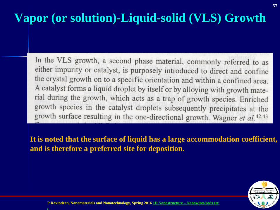
In the VLS growth an impurity/catalyst (2nd phase material) isintroduced to direct and confine the crystal growth on to a specificorientation and within a confined area. A catalyst forms a liquid dropletby itself or by alloying with growth material during the growth, whichacts a trap of growth species. Enriched growth species in the catalystdroplets subsequently precipitates at the growth surface resulting in theone-dimensional growth.
VLS theory proposed by Wagner (over 40 years ago)
8
P.Ravindran, Nanomaterials and Nanotechnology, Spring 2016 1D Nanostructure – Nanowires/rods etc.
.
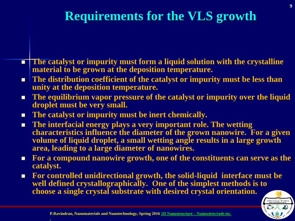
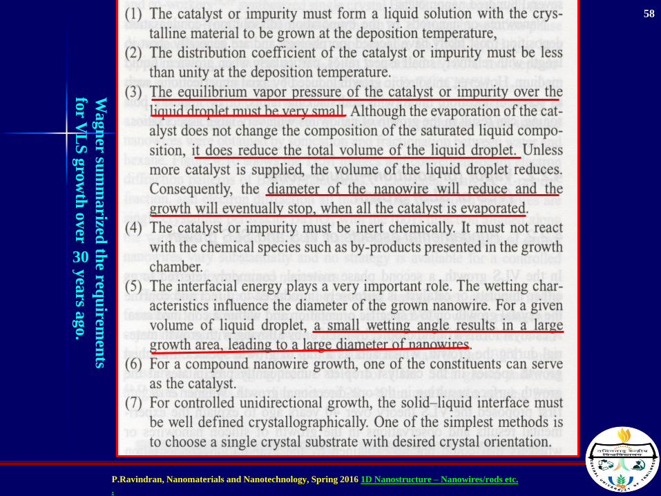
Requirements for the VLS growth
The catalyst or impurity must form a liquid solution with the crystalline material to be grown at the deposition temperature.
The distribution coefficient of the catalyst or impurity must be less than unity at the deposition temperature.
The equilibrium vapor pressure of the catalyst or impurity over the liquid droplet must be very small.
The catalyst or impurity must be inert chemically.
The interfacial energy plays a very important role. The wetting characteristics influence the diameter of the grown nanowire. For a given volume of liquid droplet, a small wetting angle results in a large growth area, leading to a large diameter of nanowires.
For a compound nanowire growth, one of the constituents can serve as the catalyst.
For controlled unidirectional growth, the solid-liquid interface must be well defined crystallographically. One of the simplest methods is to choose a single crystal substrate with desired crystal orientation.
9
P.Ravindran, Nanomaterials and Nanotechnology, Spring 2016 1D Nanostructure – Nanowires/rods etc.
.
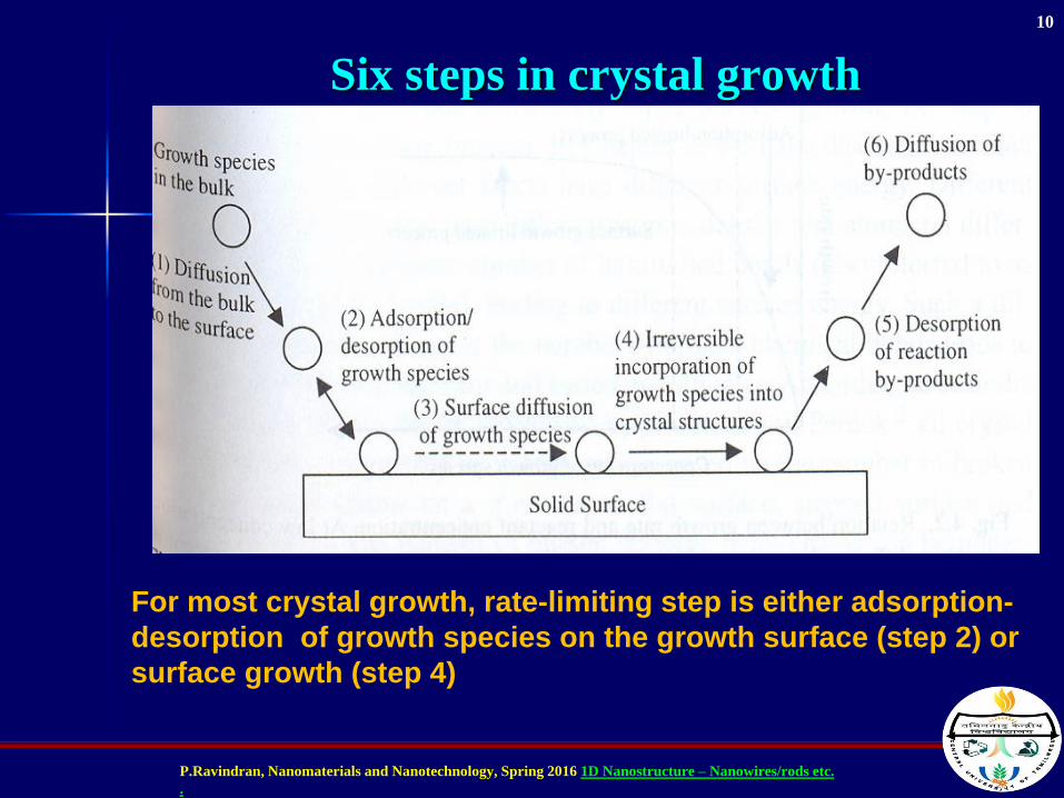
Six steps in crystal growth
For most crystal growth, rate-limiting step is either adsorption-
desorption of growth species on the growth surface (step 2) or
surface growth (step 4)
10
P.Ravindran, Nanomaterials and Nanotechnology, Spring 2016 1D Nanostructure – Nanowires/rods etc.
.
Nanowires
Nanowires are especially attractive for nanoscience studies as well
as for nanotechnology applications.
Because of their unique density of electronic states, nanowires in
the limit of small diameters are expected to exhibit significantly
different optical, electrical, and magnetic properties from their
bulk 3-D crystalline counterparts.
11
P.Ravindran, Nanomaterials and Nanotechnology, Spring 2016 1D Nanostructure – Nanowires/rods etc.
.
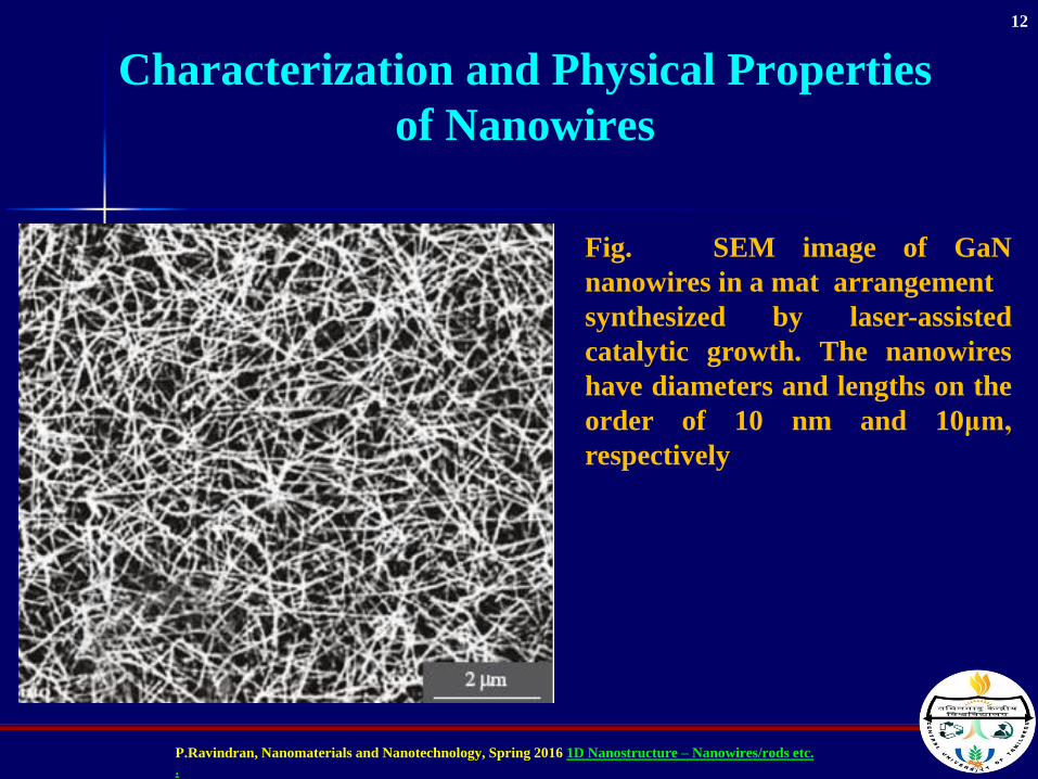
Characterization and Physical Properties
of Nanowires
Fig. SEM image of GaN
nanowires in a mat arrangement
synthesized by laser-assisted
catalytic growth. The nanowires
have diameters and lengths on the
order of 10 nm and 10μm,
respectively
12
P.Ravindran, Nanomaterials and Nanotechnology, Spring 2016 1D Nanostructure – Nanowires/rods etc.
.
Nanowires
The sizes of nanowires are typically large enough (> 1 nm in thequantum confined direction) to have local crystal structures closelyrelated to their parent materials.
Furthermore, nanowires have been shown to provide a promisingframework for applying the “bottom-up” approach for the design ofnanostructures.
Driven by:
the smaller and smaller length scales now being used in thesemiconductor, opto-electronics, and magnetics industries.
13
P.Ravindran, Nanomaterials and Nanotechnology, Spring 2016 1D Nanostructure – Nanowires/rods etc.
.
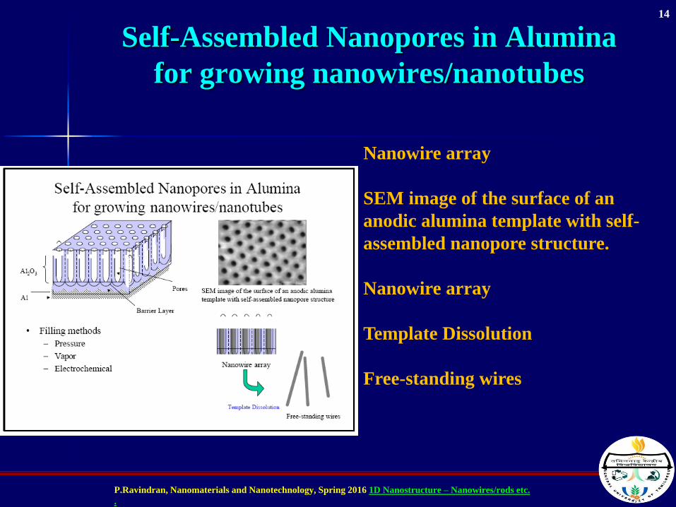
Self-Assembled Nanopores in Alumina
for growing nanowires/nanotubes
Nanowire array
SEM image of the surface of an
anodic alumina template with self-
assembled nanopore structure.
Nanowire array
Template Dissolution
Free-standing wires
14
P.Ravindran, Nanomaterials and Nanotechnology, Spring 2016 1D Nanostructure – Nanowires/rods etc.
.
Materials of Templates ( pores, self-assembled)
Al2O3 (anodic alumina )
nano-channel glass
ion track-etched polymers
and mica films
Nanowires -Template-Assisted
Synthesis
15
P.Ravindran, Nanomaterials and Nanotechnology, Spring 2016 1D Nanostructure – Nanowires/rods etc.
.
Materials of Nanowires (self-assembled)
Metal: Ag, Au, Cu, Fe, Ge, Bi, In, Sn, and Al
Semiconductors: Se, Te, GaSb, and Bi2Te3
Filling methods
– Pressure
– Vapor
– Electrochemical
Nanowires -Template-Assisted
Synthesis
16
P.Ravindran, Nanomaterials and Nanotechnology, Spring 2016 1D Nanostructure – Nanowires/rods etc.
.
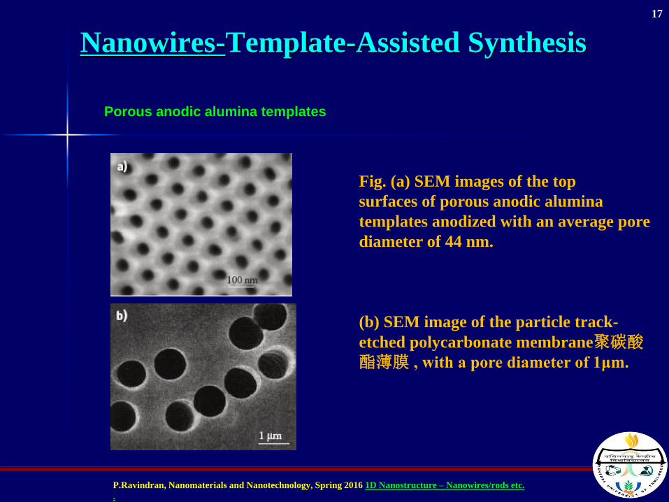
Nanowires-Template-Assisted Synthesis
Fig. (a) SEM images of the top
surfaces of porous anodic alumina
templates anodized with an average pore
diameter of 44 nm.
(b) SEM image of the particle track-
etched polycarbonate membrane聚碳酸酯薄膜 , with a pore diameter of 1μm.
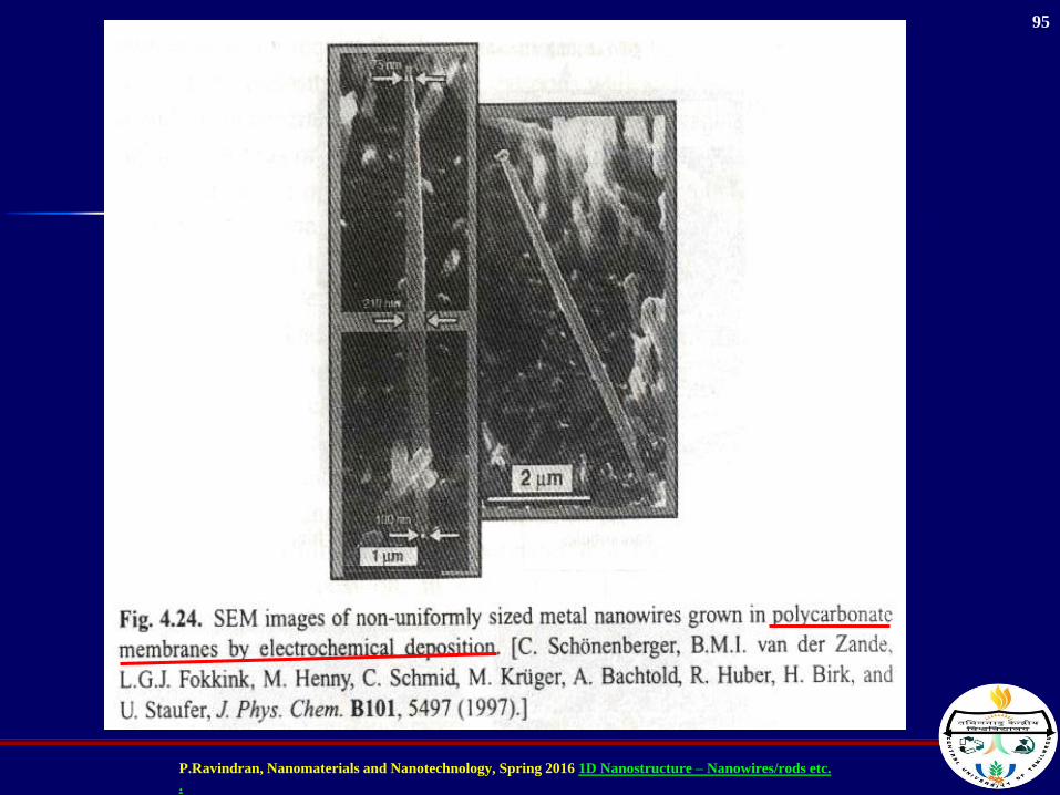
Porous anodic alumina templates
17
P.Ravindran, Nanomaterials and Nanotechnology, Spring 2016 1D Nanostructure – Nanowires/rods etc.
.
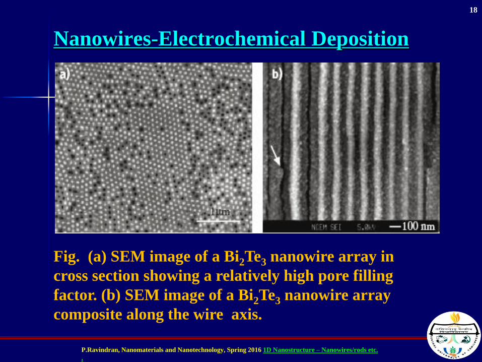
Nanowires-Electrochemical Deposition
Fig. (a) SEM image of a Bi2Te3 nanowire array in
cross section showing a relatively high pore filling
factor. (b) SEM image of a Bi2Te3 nanowire array
composite along the wire axis.
18
P.Ravindran, Nanomaterials and Nanotechnology, Spring 2016 1D Nanostructure – Nanowires/rods etc.
.
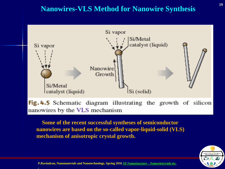
Nanowires-VLS Method for Nanowire Synthesis
Some of the recent successful syntheses of semiconductor
nanowires are based on the so-called vapor-liquid-solid (VLS)
mechanism of anisotropic crystal growth.
19
P.Ravindran, Nanomaterials and Nanotechnology, Spring 2016 1D Nanostructure – Nanowires/rods etc.
.
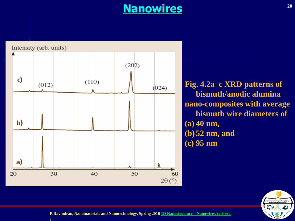
Nanowires
Fig. 4.2a–c XRD patterns of
bismuth/anodic alumina
nano-composites with average
bismuth wire diameters of
(a) 40 nm,
(b) 52 nm, and
(c) 95 nm
20
P.Ravindran, Nanomaterials and Nanotechnology, Spring 2016 1D Nanostructure – Nanowires/rods etc.
.
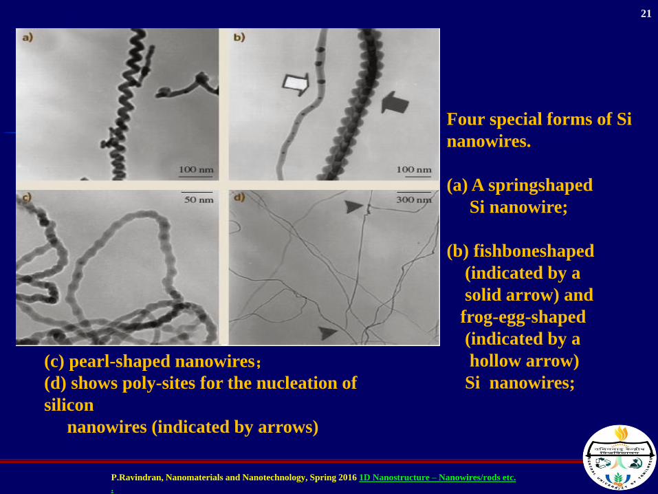
Four special forms of Si
nanowires.
(a) A springshaped
Si nanowire;
(b) fishboneshaped
(indicated by a
solid arrow) and
frog-egg-shaped
(indicated by a
hollow arrow)
Si nanowires;
(c) pearl-shaped nanowires;(d) shows poly-sites for the nucleation of
silicon
nanowires (indicated by arrows)
21
P.Ravindran, Nanomaterials and Nanotechnology, Spring 2016 1D Nanostructure – Nanowires/rods etc.
.
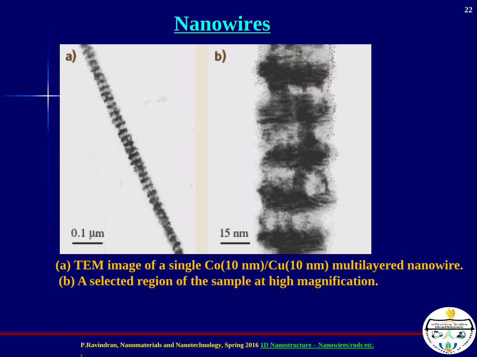
Nanowires
(a) TEM image of a single Co(10 nm)/Cu(10 nm) multilayered nanowire.
(b) A selected region of the sample at high magnification.
22
P.Ravindran, Nanomaterials and Nanotechnology, Spring 2016 1D Nanostructure – Nanowires/rods etc.
.
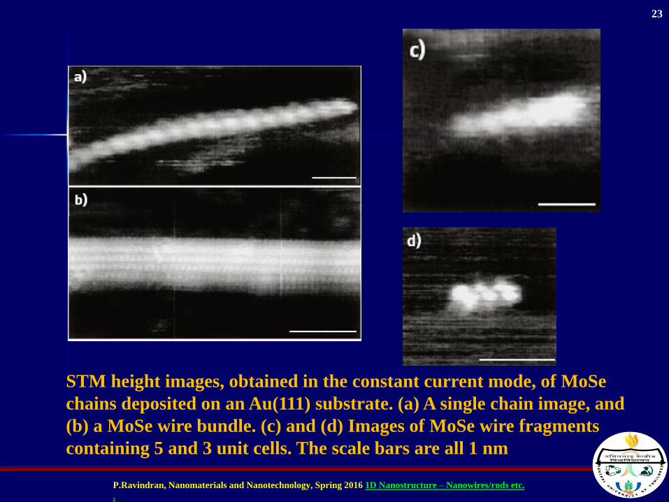
STM height images, obtained in the constant current mode, of MoSe
chains deposited on an Au(111) substrate. (a) A single chain image, and
(b) a MoSe wire bundle. (c) and (d) Images of MoSe wire fragments
containing 5 and 3 unit cells. The scale bars are all 1 nm
23
P.Ravindran, Nanomaterials and Nanotechnology, Spring 2016 1D Nanostructure – Nanowires/rods etc.
.
Nanowires
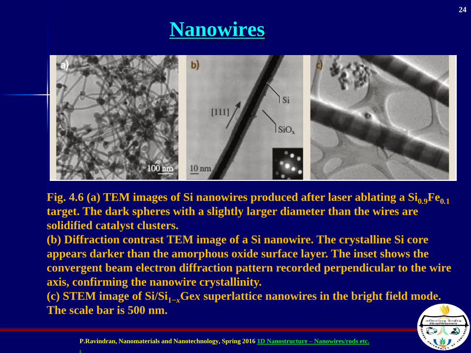
Fig. 4.6 (a) TEM images of Si nanowires produced after laser ablating a Si0.9Fe0.1
target. The dark spheres with a slightly larger diameter than the wires are
solidified catalyst clusters.
(b) Diffraction contrast TEM image of a Si nanowire. The crystalline Si core
appears darker than the amorphous oxide surface layer. The inset shows the
convergent beam electron diffraction pattern recorded perpendicular to the wire
axis, confirming the nanowire crystallinity.
(c) STEM image of Si/Si1−xGex superlattice nanowires in the bright field mode.
The scale bar is 500 nm.
24
P.Ravindran, Nanomaterials and Nanotechnology, Spring 2016 1D Nanostructure – Nanowires/rods etc.
.
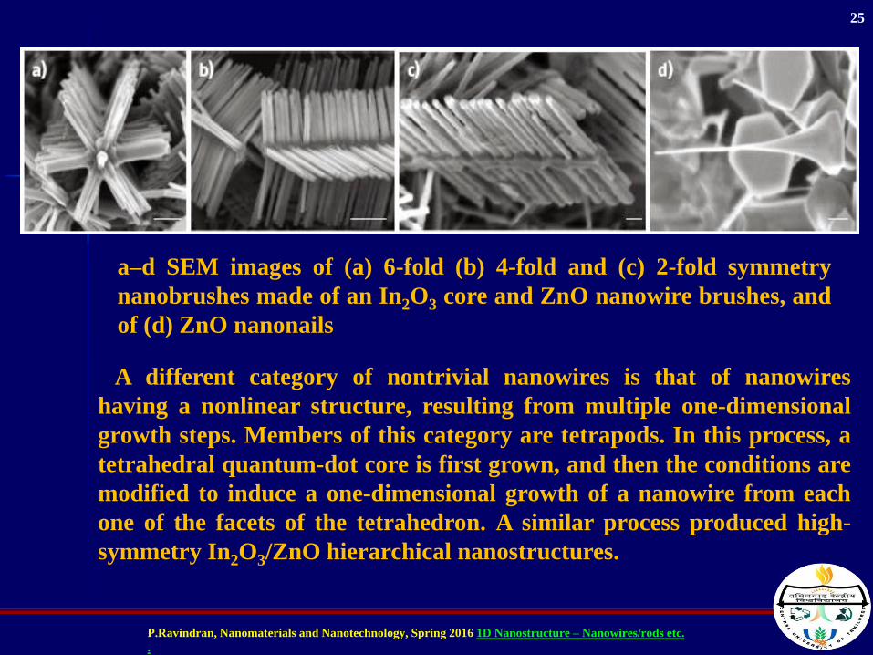
a–d SEM images of (a) 6-fold (b) 4-fold and (c) 2-fold symmetry
nanobrushes made of an In2O3 core and ZnO nanowire brushes, and
of (d) ZnO nanonails
A different category of nontrivial nanowires is that of nanowires
having a nonlinear structure, resulting from multiple one-dimensional
growth steps. Members of this category are tetrapods. In this process, a
tetrahedral quantum-dot core is first grown, and then the conditions are
modified to induce a one-dimensional growth of a nanowire from each
one of the facets of the tetrahedron. A similar process produced high-
symmetry In2O3/ZnO hierarchical nanostructures.
25
P.Ravindran, Nanomaterials and Nanotechnology, Spring 2016 1D Nanostructure – Nanowires/rods etc.
.
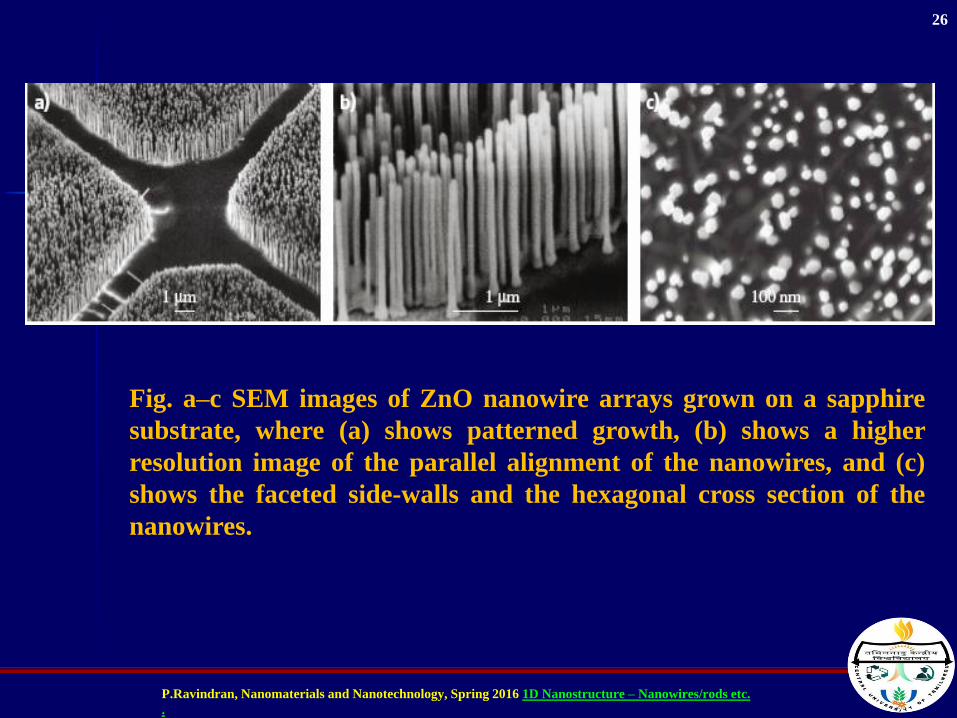
Fig. a–c SEM images of ZnO nanowire arrays grown on a sapphire
substrate, where (a) shows patterned growth, (b) shows a higher
resolution image of the parallel alignment of the nanowires, and (c)
shows the faceted side-walls and the hexagonal cross section of the
nanowires.
26
P.Ravindran, Nanomaterials and Nanotechnology, Spring 2016 1D Nanostructure – Nanowires/rods etc.
.
Nanowires -Characterization and Physical
Properties
Because of their unique density of electronic states, nanowires in thelimit of small diameters are expected to exhibit significantly differentoptical, electrical, and magnetic properties from their bulk 3-Dcrystalline counterparts.
Increased surface area, very high density of electronic states enhancedexciton binding energy, diameter-dependent bandgap, and increasedsurface scattering for electrons are just some of the ways in whichnanowires differ from their corresponding bulk materials.
27
P.Ravindran, Nanomaterials and Nanotechnology, Spring 2016 1D Nanostructure – Nanowires/rods etc.
.
Nanowires Applications
“Bottom-up” to form nanowire diodes
Schottky diodes can be formed by contacting a GaNnanowire with Al electrodes.
p-n junction diodes can be formed at the crossing of twonanowires, such as the crossing of n and p-type InP nanowiresdoped by Te and Zn, or Si nanowires doped by phosphorus(n-type) and boron (p-type).
28
P.Ravindran, Nanomaterials and Nanotechnology, Spring 2016 1D Nanostructure – Nanowires/rods etc.
.
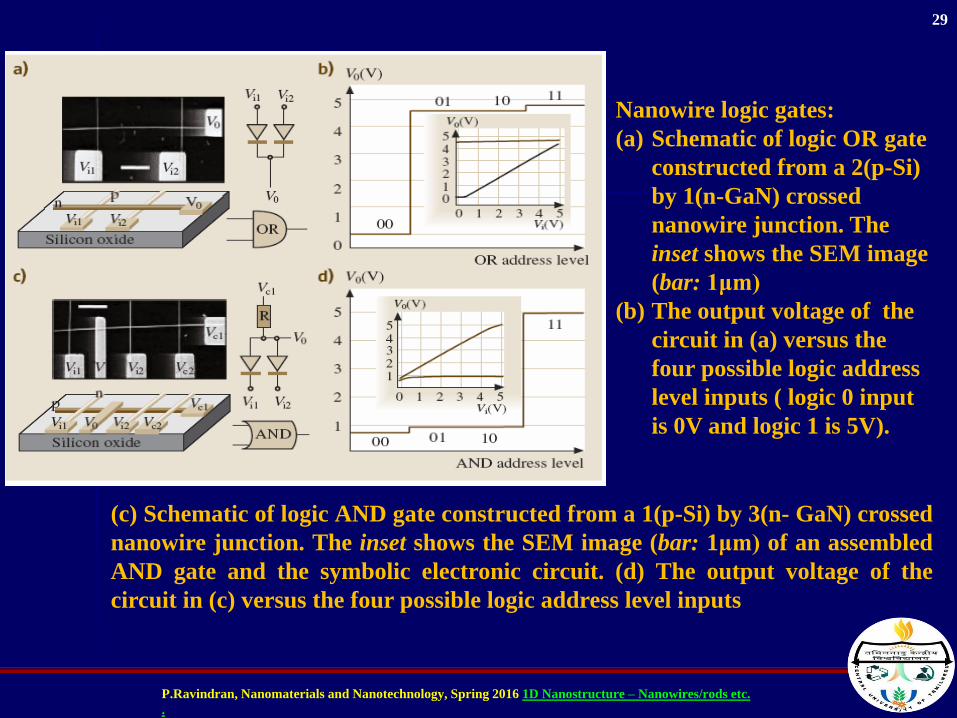
Nanowire logic gates:
(a) Schematic of logic OR gate
constructed from a 2(p-Si)
by 1(n-GaN) crossed
nanowire junction. The
inset shows the SEM image
(bar: 1μm)
(b) The output voltage of the
circuit in (a) versus the
four possible logic address
level inputs ( logic 0 input
is 0V and logic 1 is 5V).
(c) Schematic of logic AND gate constructed from a 1(p-Si) by 3(n- GaN) crossed
nanowire junction. The inset shows the SEM image (bar: 1μm) of an assembled
AND gate and the symbolic electronic circuit. (d) The output voltage of the
circuit in (c) versus the four possible logic address level inputs
29
P.Ravindran, Nanomaterials and Nanotechnology, Spring 2016 1D Nanostructure – Nanowires/rods etc.
.
Nanowires
In addition to the crossing of two distinctive nanowires, heterogeneousjunctions have also been constructed inside a singlewire, either along thewire axis in the form of a nanowire superlattice or perpendicular to thewire axis by forming a core-shell structure of silicon and germanium.
These various nanowire junctions not only possess similar currentrectifying properties as expected for bulk semiconductor devices, butthey also exhibit electro-luminescence (EL) as of a crossed junction of nand p-type InP nanowires that may be interesting for optoelectronicapplications.
30
P.Ravindran, Nanomaterials and Nanotechnology, Spring 2016 1D Nanostructure – Nanowires/rods etc.
.
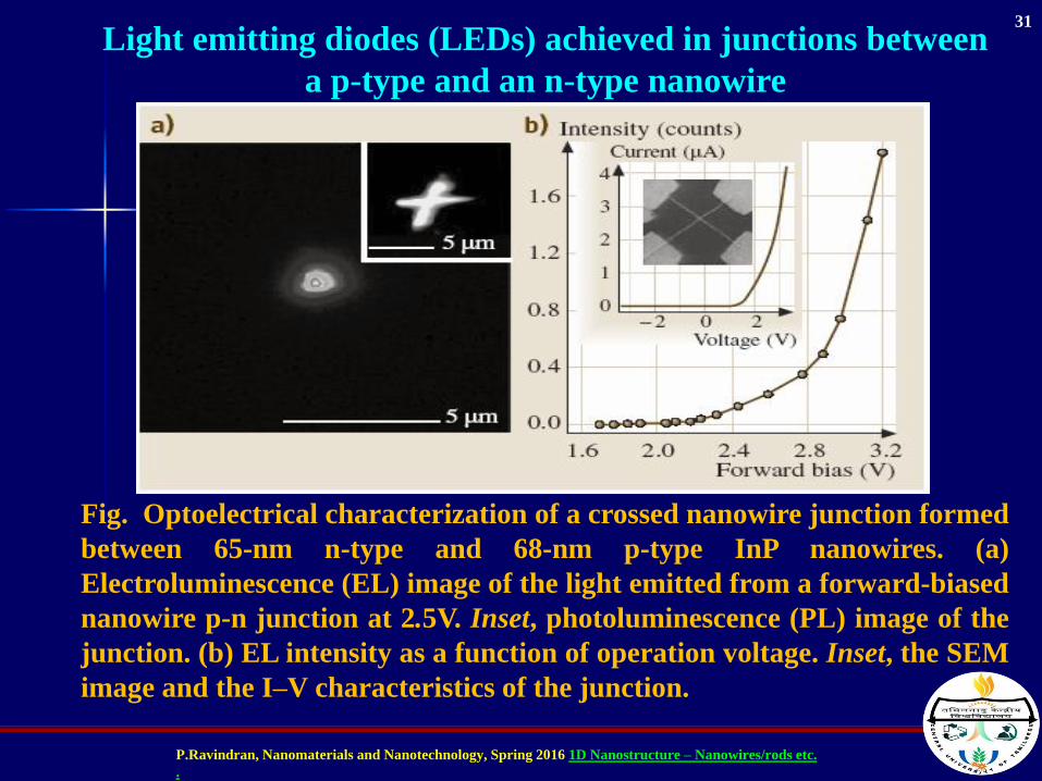
Fig. Optoelectrical characterization of a crossed nanowire junction formed
between 65-nm n-type and 68-nm p-type InP nanowires. (a)
Electroluminescence (EL) image of the light emitted from a forward-biased
nanowire p-n junction at 2.5V. Inset, photoluminescence (PL) image of the
junction. (b) EL intensity as a function of operation voltage. Inset, the SEM
image and the I–V characteristics of the junction.
Light emitting diodes (LEDs) achieved in junctions between
a p-type and an n-type nanowire
31
P.Ravindran, Nanomaterials and Nanotechnology, Spring 2016 1D Nanostructure – Nanowires/rods etc.
.
In addition to the two-terminal nanowire devices, such as the p-njunctions described above, it is found that the conductance of asemiconductor nanowire can be significantly modified by applyingvoltage at a third gate terminal, implying the utilization of nanowiresas a field-effect transistor (FET).
This gate terminal can either be the substrate, a separate metal contactlocated close to the nanowire, or another nanowire with a thick oxidecoating in the crossed nanowire junction configuration.
Nanowires as a field-effect transistor (FET)
32
P.Ravindran, Nanomaterials and Nanotechnology, Spring 2016 1D Nanostructure – Nanowires/rods etc.
.
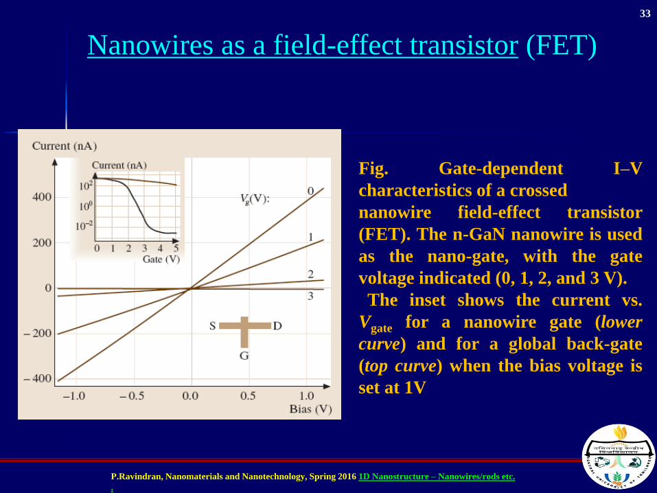
Fig. Gate-dependent I–V
characteristics of a crossed
nanowire field-effect transistor
(FET). The n-GaN nanowire is used
as the nano-gate, with the gate
voltage indicated (0, 1, 2, and 3 V).
The inset shows the current vs.
Vgate for a nanowire gate (lower
curve) and for a global back-gate
(top curve) when the bias voltage is
set at 1V
Nanowires as a field-effect transistor (FET)
33
P.Ravindran, Nanomaterials and Nanotechnology, Spring 2016 1D Nanostructure – Nanowires/rods etc.
.
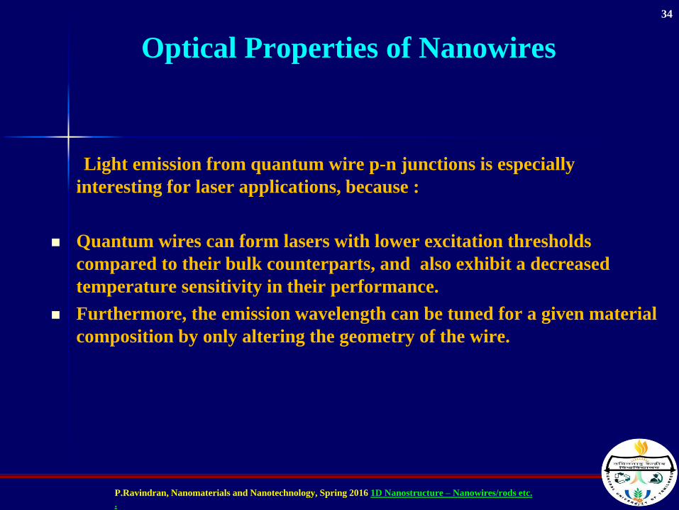
Optical Properties of Nanowires
Light emission from quantum wire p-n junctions is especially
interesting for laser applications, because :
Quantum wires can form lasers with lower excitation thresholds
compared to their bulk counterparts, and also exhibit a decreased
temperature sensitivity in their performance.
Furthermore, the emission wavelength can be tuned for a given material
composition by only altering the geometry of the wire.
34
P.Ravindran, Nanomaterials and Nanotechnology, Spring 2016 1D Nanostructure – Nanowires/rods etc.
.
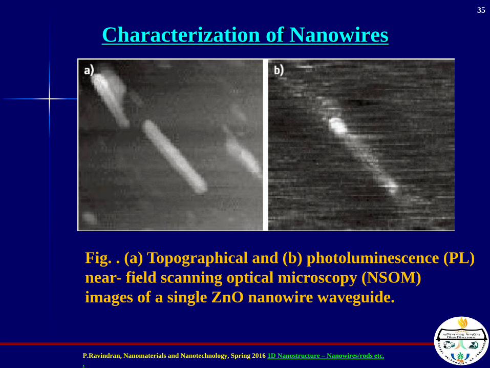
Fig. . (a) Topographical and (b) photoluminescence (PL)
near- field scanning optical microscopy (NSOM)
images of a single ZnO nanowire waveguide.
Characterization of Nanowires
35
P.Ravindran, Nanomaterials and Nanotechnology, Spring 2016 1D Nanostructure – Nanowires/rods etc.
.
Nanowires
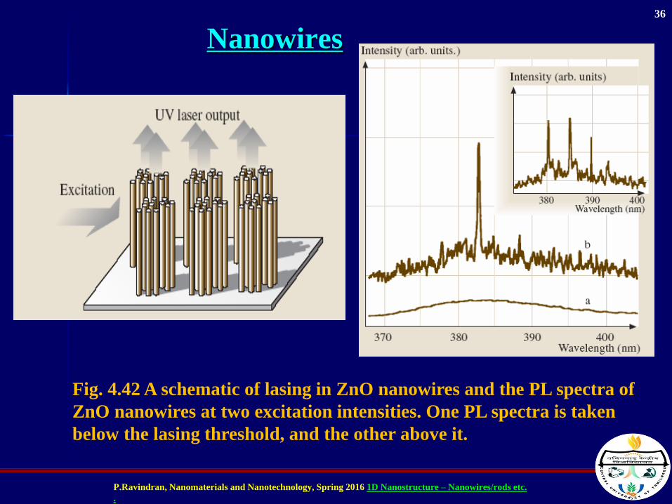
Fig. 4.42 A schematic of lasing in ZnO nanowires and the PL spectra of
ZnO nanowires at two excitation intensities. One PL spectra is taken
below the lasing threshold, and the other above it.
36
P.Ravindran, Nanomaterials and Nanotechnology, Spring 2016 1D Nanostructure – Nanowires/rods etc.
.
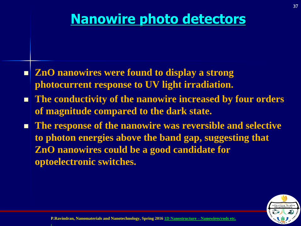
Nanowire photo detectors
ZnO nanowires were found to display a strong
photocurrent response to UV light irradiation.
The conductivity of the nanowire increased by four orders
of magnitude compared to the dark state.
The response of the nanowire was reversible and selective
to photon energies above the band gap, suggesting that
ZnO nanowires could be a good candidate for
optoelectronic switches.
37
P.Ravindran, Nanomaterials and Nanotechnology, Spring 2016 1D Nanostructure – Nanowires/rods etc.
.
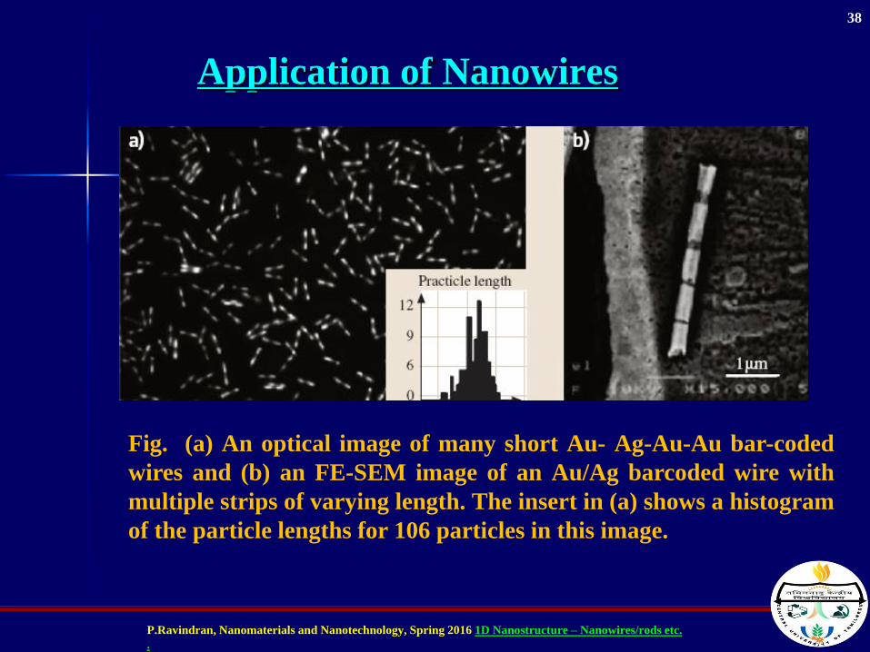
Application of Nanowires
Fig. (a) An optical image of many short Au- Ag-Au-Au bar-coded
wires and (b) an FE-SEM image of an Au/Ag barcoded wire with
multiple strips of varying length. The insert in (a) shows a histogram
of the particle lengths for 106 particles in this image.
38
P.Ravindran, Nanomaterials and Nanotechnology, Spring 2016 1D Nanostructure – Nanowires/rods etc.
.
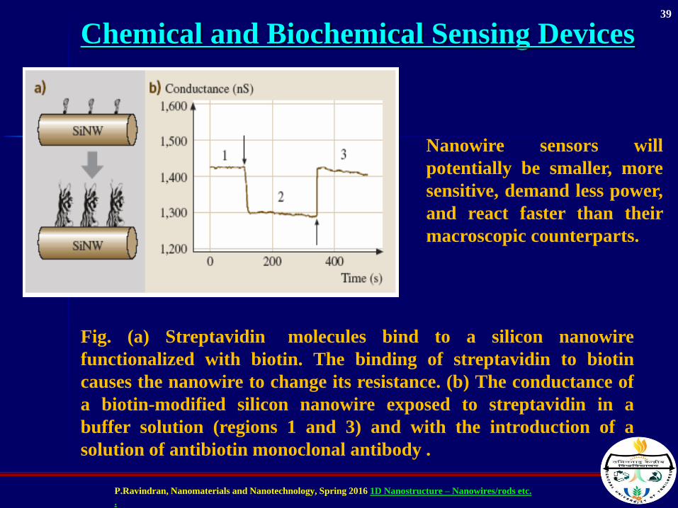
Chemical and Biochemical Sensing Devices
Fig. (a) Streptavidin molecules bind to a silicon nanowire
functionalized with biotin. The binding of streptavidin to biotin
causes the nanowire to change its resistance. (b) The conductance of
a biotin-modified silicon nanowire exposed to streptavidin in a
buffer solution (regions 1 and 3) and with the introduction of a
solution of antibiotin monoclonal antibody .
Nanowire sensors will
potentially be smaller, more
sensitive, demand less power,
and react faster than their
macroscopic counterparts.
39
P.Ravindran, Nanomaterials and Nanotechnology, Spring 2016 1D Nanostructure – Nanowires/rods etc.
.
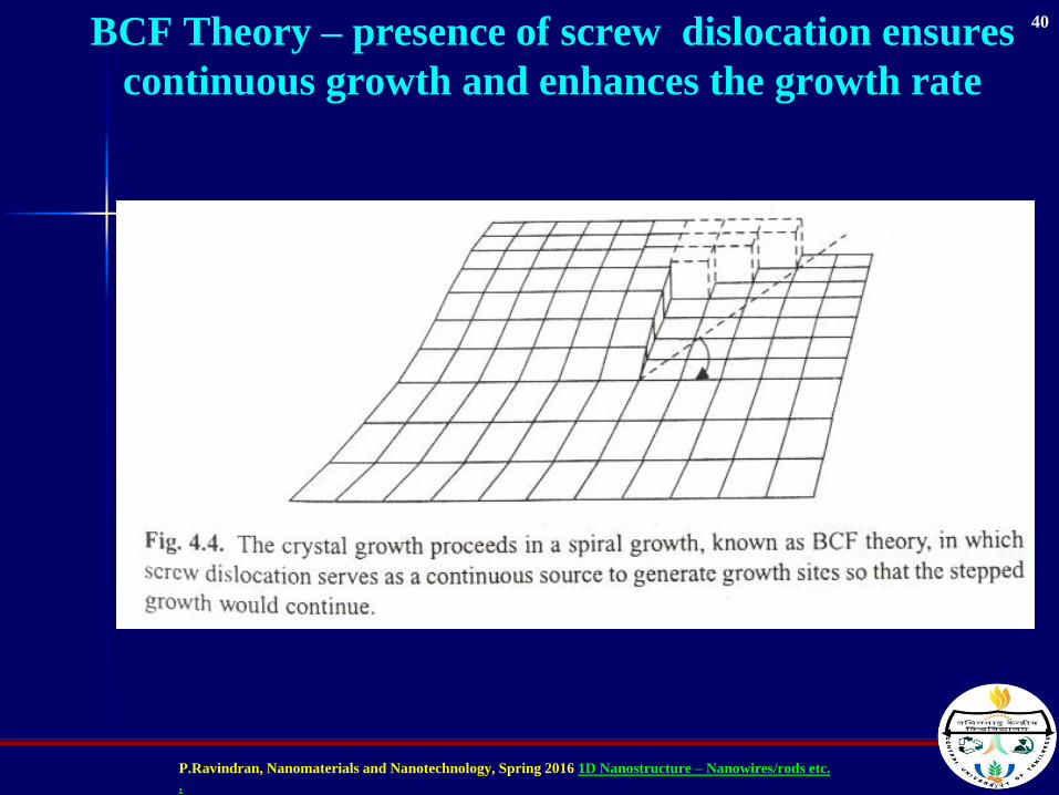
BCF Theory – presence of screw dislocation ensures
continuous growth and enhances the growth rate
40
P.Ravindran, Nanomaterials and Nanotechnology, Spring 2016 1D Nanostructure – Nanowires/rods etc.
.
Mechanism leading to formation of nanowire
The growth rate of a facet increases with an increased
density of screw dislocations parallel to the growth
direction. It is known that different facets can have a
significantly different ability to accommodate dislocations.
The presence of dislocations on a certain facet can result in
anisotropic growth, leading to the formation of nanowire
or nanorods.
41
P.Ravindran, Nanomaterials and Nanotechnology, Spring 2016 1D Nanostructure – Nanowires/rods etc.
.
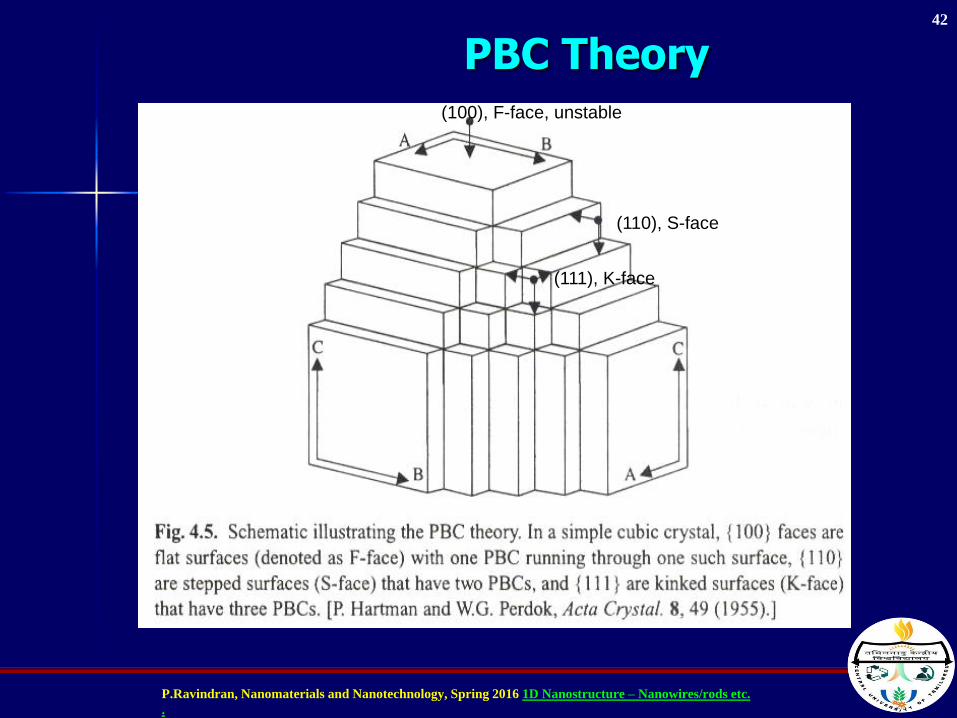
PBC Theory(100), F-face, unstable
(110), S-face
(111), K-face
42
P.Ravindran, Nanomaterials and Nanotechnology, Spring 2016 1D Nanostructure – Nanowires/rods etc.
.
Mechanism leading to Anisotropic Growth
Therefore, α = 1 for {111} and {110}, α< 1 for {100}. Thisleads to that growth rate for {111}, {110} is greater thanthat for {100}. For both {111} and {110}, the growthprocess is always adsorption limited. Facets with highgrowth rate (high surface energy) disappears while facetswith low growth rate (low surface energy) survives. Thisleads to anisotropic growth and results in nanowires. Inaddition, defects-induced growth and impurity-inhibitedgrowth are the possible mechanisms for growth along axisof nanowires. A low supersaturation is required foranisotropic growth. A higher supersaturation supportsbulk crystal growth or homogeneous nucleation leading toformation of polycrystalline or powder.
43
P.Ravindran, Nanomaterials and Nanotechnology, Spring 2016 1D Nanostructure – Nanowires/rods etc.
.
Growth of Single Crystal Nanobelts of
Semiconducting or metal oxides
Evaporating the metal oxides (ZnO, SnO2, In2O3, CdO) athigh temperatures under a vacuum of 300 torr andcondensing on an alumina substrate, placed inside thesame alumina tube furnace, at relatively low temperature.
Or heating the metal oxide or metal nanoparticles atT=780 - 820oC in air, Nanorods can be obtained dependingupon annealing T and time. Nanowires such as ZnO,Ga2O3, MgO, CuO or Si3N4 and SiC can be made by thismethod.
44
P.Ravindran, Nanomaterials and Nanotechnology, Spring 2016 1D Nanostructure – Nanowires/rods etc.
.
45
P.Ravindran, Nanomaterials and Nanotechnology, Spring 2016 1D Nanostructure – Nanowires/rods etc.
.
46
P.Ravindran, Nanomaterials and Nanotechnology, Spring 2016 1D Nanostructure – Nanowires/rods etc.
.
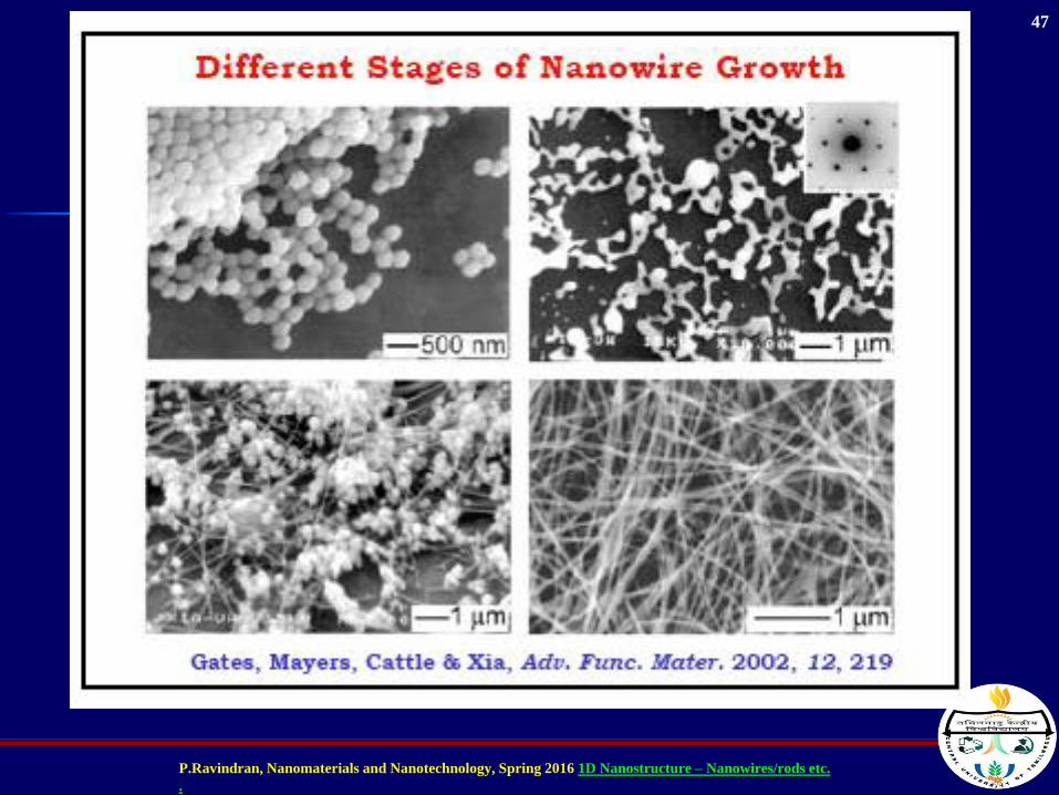
47
P.Ravindran, Nanomaterials and Nanotechnology, Spring 2016 1D Nanostructure – Nanowires/rods etc.
.
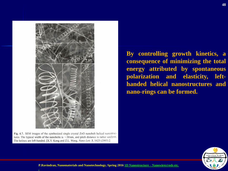
By controlling growth kinetics, a
consequence of minimizing the total
energy attributed by spontaneous
polarization and elasticity, left-
handed helical nanostructures and
nano-rings can be formed.
48
P.Ravindran, Nanomaterials and Nanotechnology, Spring 2016 1D Nanostructure – Nanowires/rods etc.
.
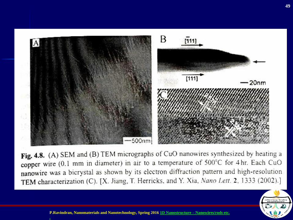
49
P.Ravindran, Nanomaterials and Nanotechnology, Spring 2016 1D Nanostructure – Nanowires/rods etc.
.
Dissolution and Condensation Growth
The growth species first dissolve into a solvent or a
solution, and then diffuse through the solvent and
deposit onto the surface resulting growth of
nanowires.
50
P.Ravindran, Nanomaterials and Nanotechnology, Spring 2016 1D Nanostructure – Nanowires/rods etc.
.
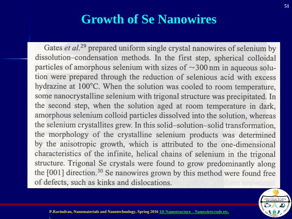
Growth of Se Nanowires
51
P.Ravindran, Nanomaterials and Nanotechnology, Spring 2016 1D Nanostructure – Nanowires/rods etc.
.
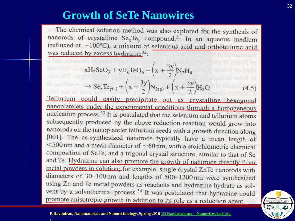
Growth of SeTe Nanowires52
P.Ravindran, Nanomaterials and Nanotechnology, Spring 2016 1D Nanostructure – Nanowires/rods etc.
.
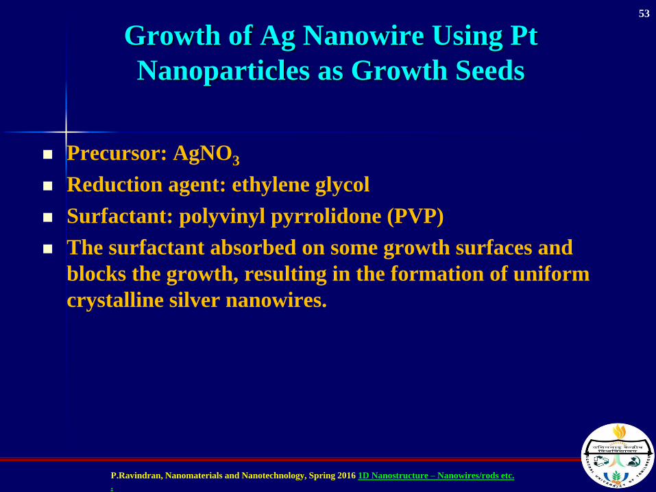
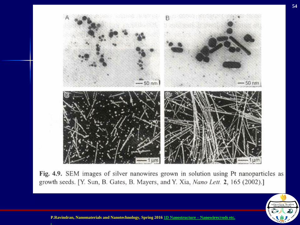
Growth of Ag Nanowire Using Pt
Nanoparticles as Growth Seeds
Precursor: AgNO3
Reduction agent: ethylene glycol
Surfactant: polyvinyl pyrrolidone (PVP)
The surfactant absorbed on some growth surfaces and
blocks the growth, resulting in the formation of uniform
crystalline silver nanowires.
53
P.Ravindran, Nanomaterials and Nanotechnology, Spring 2016 1D Nanostructure – Nanowires/rods etc.
.
54
P.Ravindran, Nanomaterials and Nanotechnology, Spring 2016 1D Nanostructure – Nanowires/rods etc.
.
55
P.Ravindran, Nanomaterials and Nanotechnology, Spring 2016 1D Nanostructure – Nanowires/rods etc.
.
Disadvantages of Evaporation – Condensation
Deposition
Nanowire grown by EC most likely have facetedmorphology and are generally short in length withrelatively small aspect ratios, particular when grown inliquid medium. However, anisotropic growth induced byaxial imperfections, such as screw dislocation, microtwinsand stacking faults, or by impurity poisoning, can result inthe growth of nanowires with large aspect ratios.
56
P.Ravindran, Nanomaterials and Nanotechnology, Spring 2016 1D Nanostructure – Nanowires/rods etc.
.
Vapor (or solution)-Liquid-solid (VLS) Growth
It is noted that the surface of liquid has a large accommodation coefficient,
and is therefore a preferred site for deposition.
57
P.Ravindran, Nanomaterials and Nanotechnology, Spring 2016 1D Nanostructure – Nanowires/rods etc.
.
Wagn
er sum
marized
the req
uirem
ents
for V
LS
gro
wth
over
30yea
rs ago.
58
P.Ravindran, Nanomaterials and Nanotechnology, Spring 2016 1D Nanostructure – Nanowires/rods etc.
.
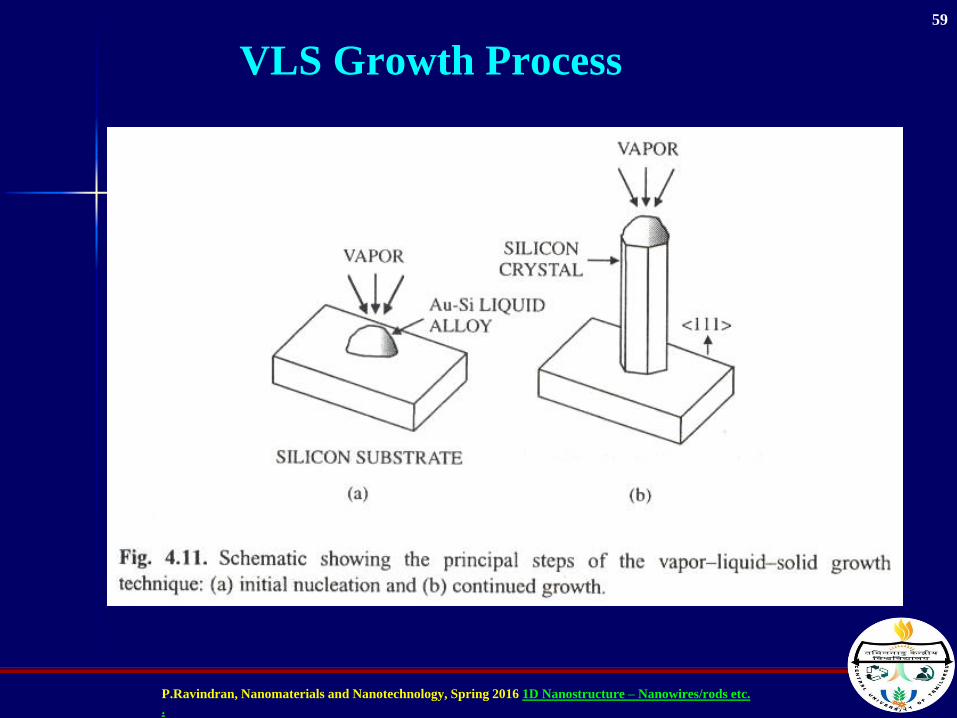
VLS Growth Process
59
P.Ravindran, Nanomaterials and Nanotechnology, Spring 2016 1D Nanostructure – Nanowires/rods etc.
.
60
P.Ravindran, Nanomaterials and Nanotechnology, Spring 2016 1D Nanostructure – Nanowires/rods etc.
.
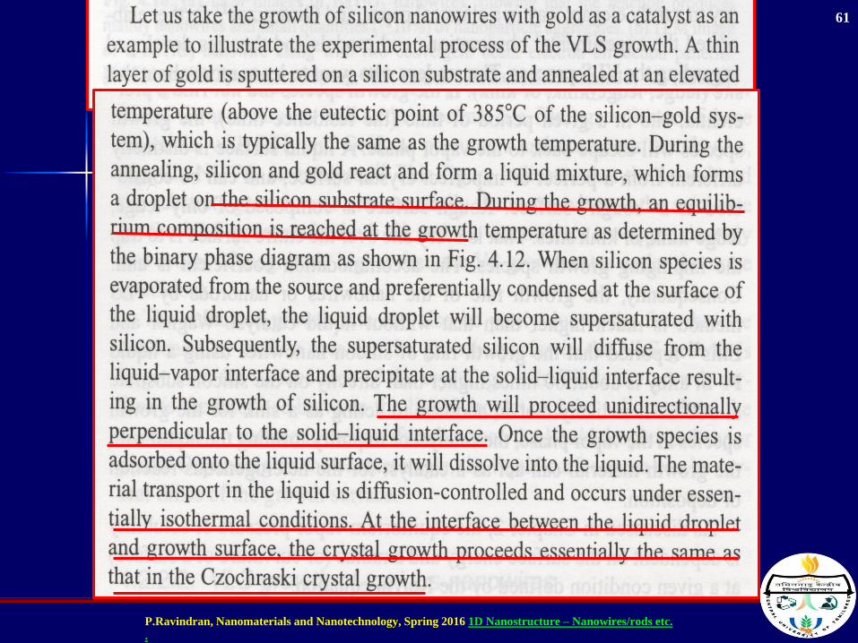
61
P.Ravindran, Nanomaterials and Nanotechnology, Spring 2016 1D Nanostructure – Nanowires/rods etc.
.
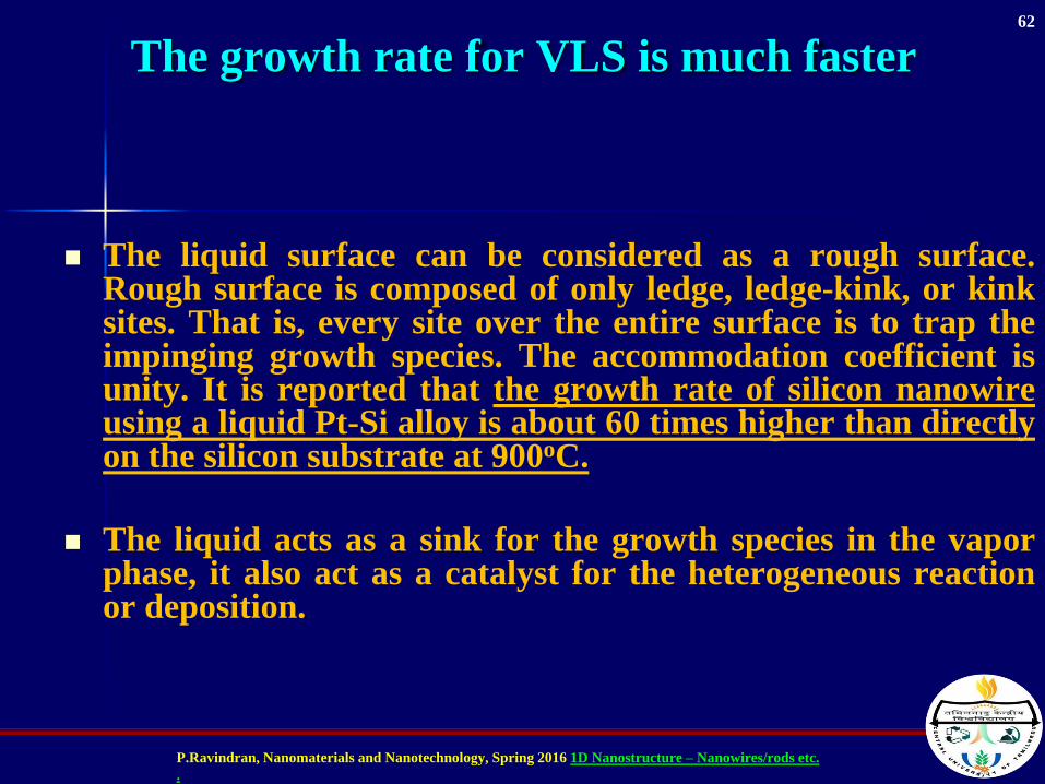
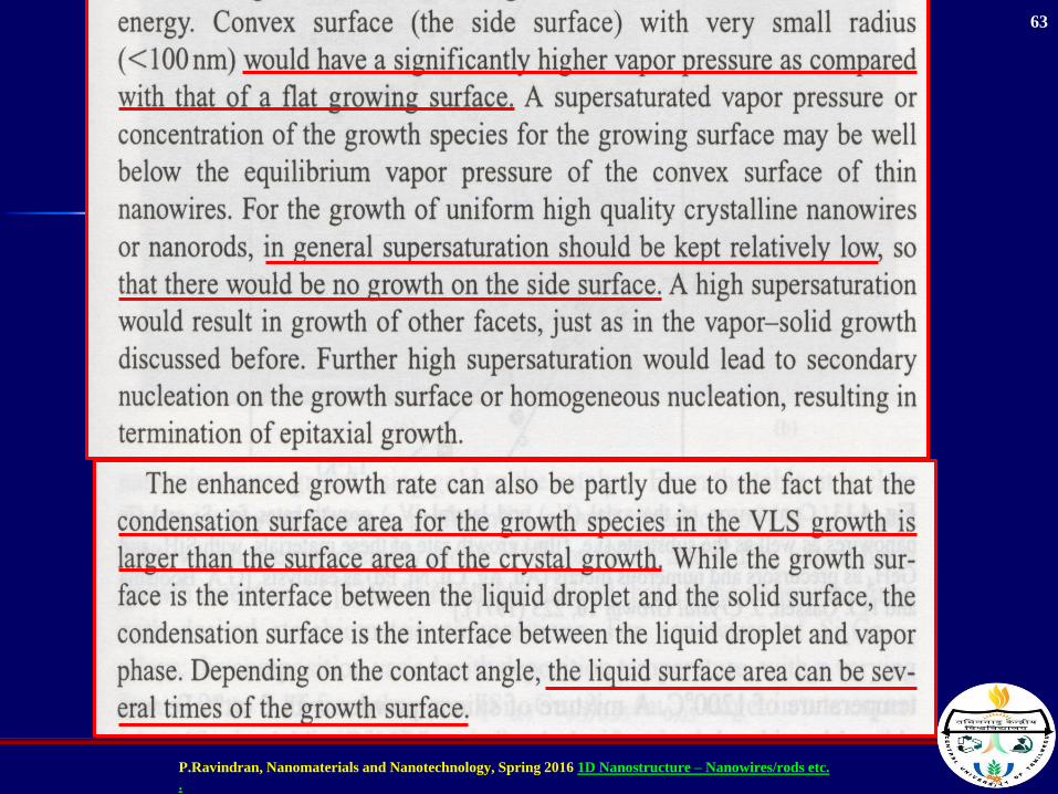
The growth rate for VLS is much faster
The liquid surface can be considered as a rough surface.Rough surface is composed of only ledge, ledge-kink, or kinksites. That is, every site over the entire surface is to trap theimpinging growth species. The accommodation coefficient isunity. It is reported that the growth rate of silicon nanowireusing a liquid Pt-Si alloy is about 60 times higher than directlyon the silicon substrate at 900oC.
The liquid acts as a sink for the growth species in the vaporphase, it also act as a catalyst for the heterogeneous reactionor deposition.
62
P.Ravindran, Nanomaterials and Nanotechnology, Spring 2016 1D Nanostructure – Nanowires/rods etc.
.
63
P.Ravindran, Nanomaterials and Nanotechnology, Spring 2016 1D Nanostructure – Nanowires/rods etc.
.
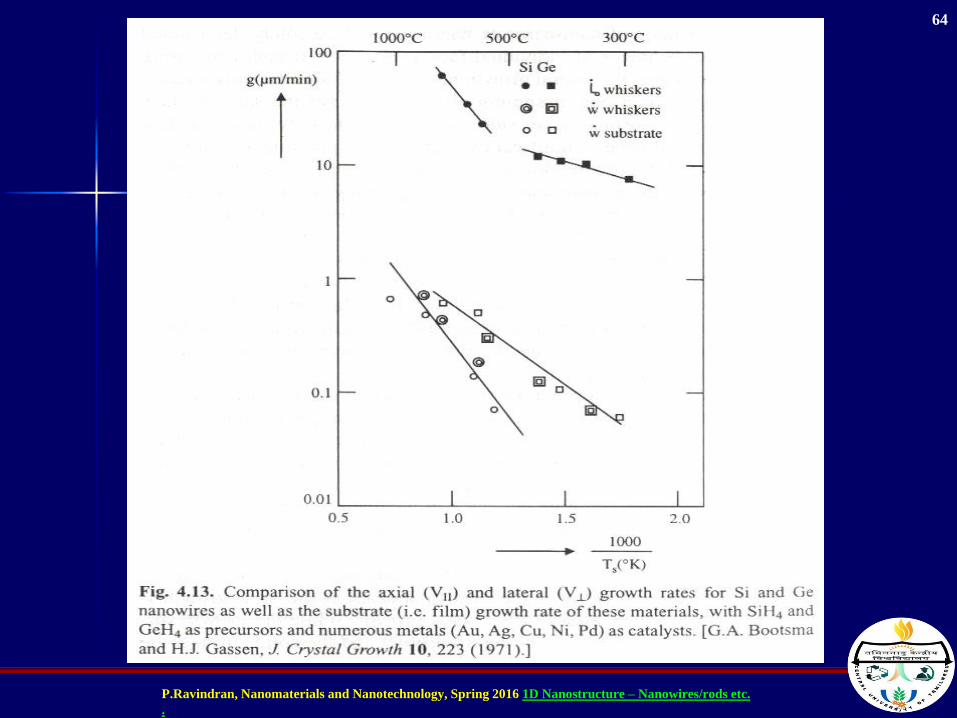
64
P.Ravindran, Nanomaterials and Nanotechnology, Spring 2016 1D Nanostructure – Nanowires/rods etc.
.
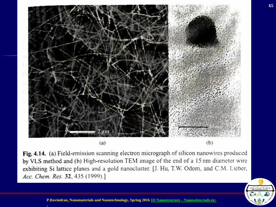
65
P.Ravindran, Nanomaterials and Nanotechnology, Spring 2016 1D Nanostructure – Nanowires/rods etc.
.
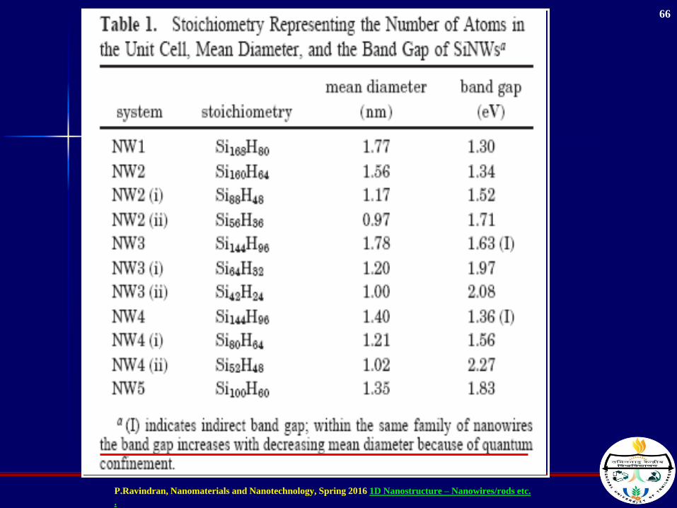
66
P.Ravindran, Nanomaterials and Nanotechnology, Spring 2016 1D Nanostructure – Nanowires/rods etc.
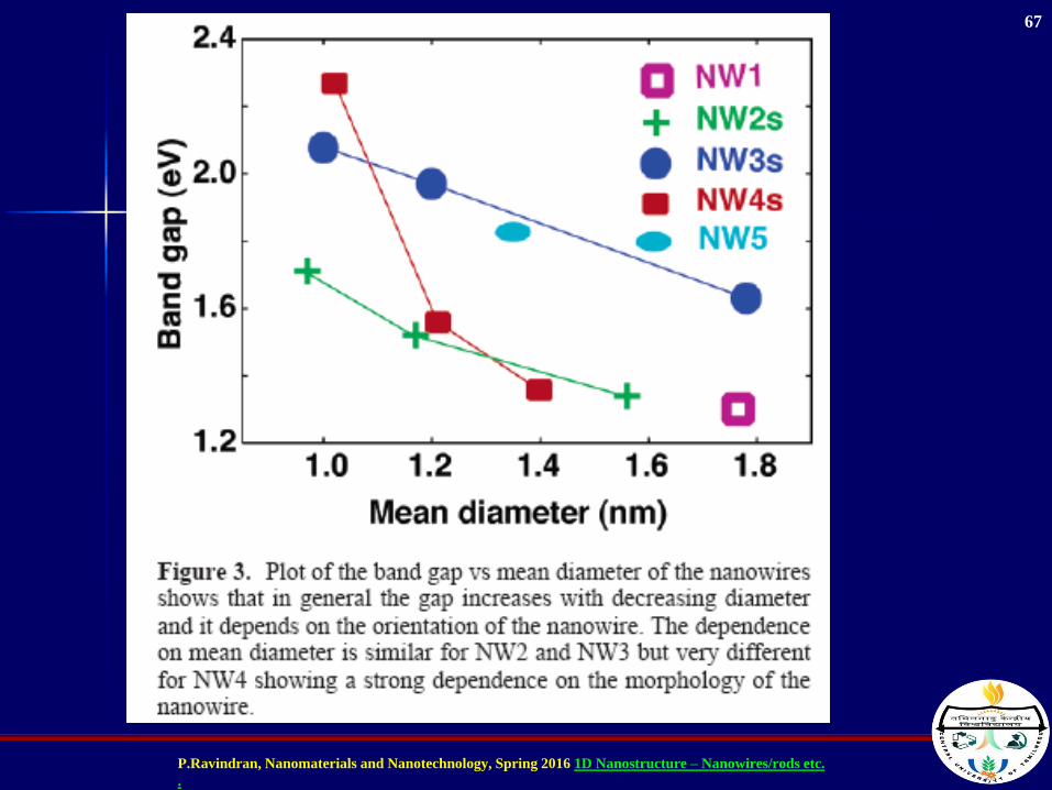
.
67
P.Ravindran, Nanomaterials and Nanotechnology, Spring 2016 1D Nanostructure – Nanowires/rods etc.
.
Compound Semiconductor Nanowires
Nanowires of binary group III-V materials (GaAs, GaP,
InAs, and InP), ternary III-V materials (GaAs/P,
InAs/P), binary II-VI compounds (ZnS, ZnSe, CdS, and
CdSe), and binary IV-IV SiGe alloys have been made in
bulk quantities as high purity (>90%) single crystals.
68
P.Ravindran, Nanomaterials and Nanotechnology, Spring 2016 1D Nanostructure – Nanowires/rods etc.
.
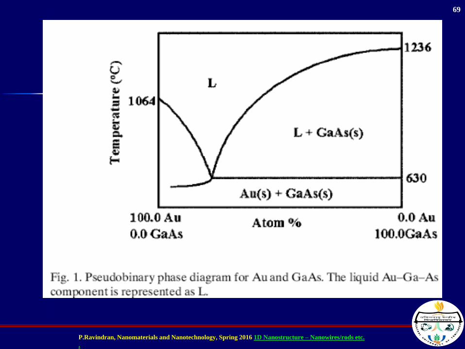
69
P.Ravindran, Nanomaterials and Nanotechnology, Spring 2016 1D Nanostructure – Nanowires/rods etc.
.
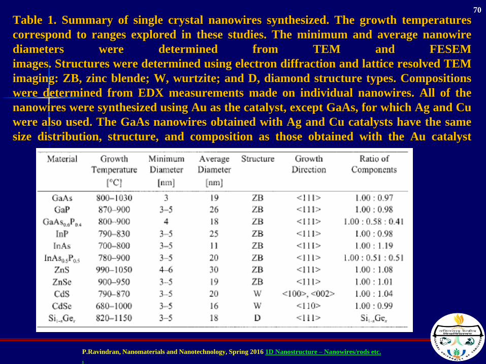
Table 1. Summary of single crystal nanowires synthesized. The growth temperatures
correspond to ranges explored in these studies. The minimum and average nanowire
diameters were determined from TEM and FESEM
images. Structures were determined using electron diffraction and lattice resolved TEM
were determined from EDX measurements made on individual nanowires. All of the
nanowires were synthesized using Au as the catalyst, except GaAs, for which Ag and Cu
were also used. The GaAs nanowires obtained with Ag and Cu catalysts have the same
size distribution, structure, and composition as those obtained with the Au catalyst
70
P.Ravindran, Nanomaterials and Nanotechnology, Spring 2016 1D Nanostructure – Nanowires/rods etc.
.
Choice of Catalyst
The catalysts for VLS growth can be chosen in the absenceof detailed phase diagrams by identifying metals in whichthe nanowire component elements are soluble in the liquidphase but that do not form solid compounds more stablethan the desired nanowire phase; i.e., the ideal metalcatalyst should be physically active but chemically stable.From this perspective the noble metal Au should representa good starting point for many materials. This noble metalalso has been used in the past for the VLS growth of surfacesupported nanowires by metal-organic chemical vapordeposition (MOCVD).
71
P.Ravindran, Nanomaterials and Nanotechnology, Spring 2016 1D Nanostructure – Nanowires/rods etc.
.
72
P.Ravindran, Nanomaterials and Nanotechnology, Spring 2016 1D Nanostructure – Nanowires/rods etc.
.
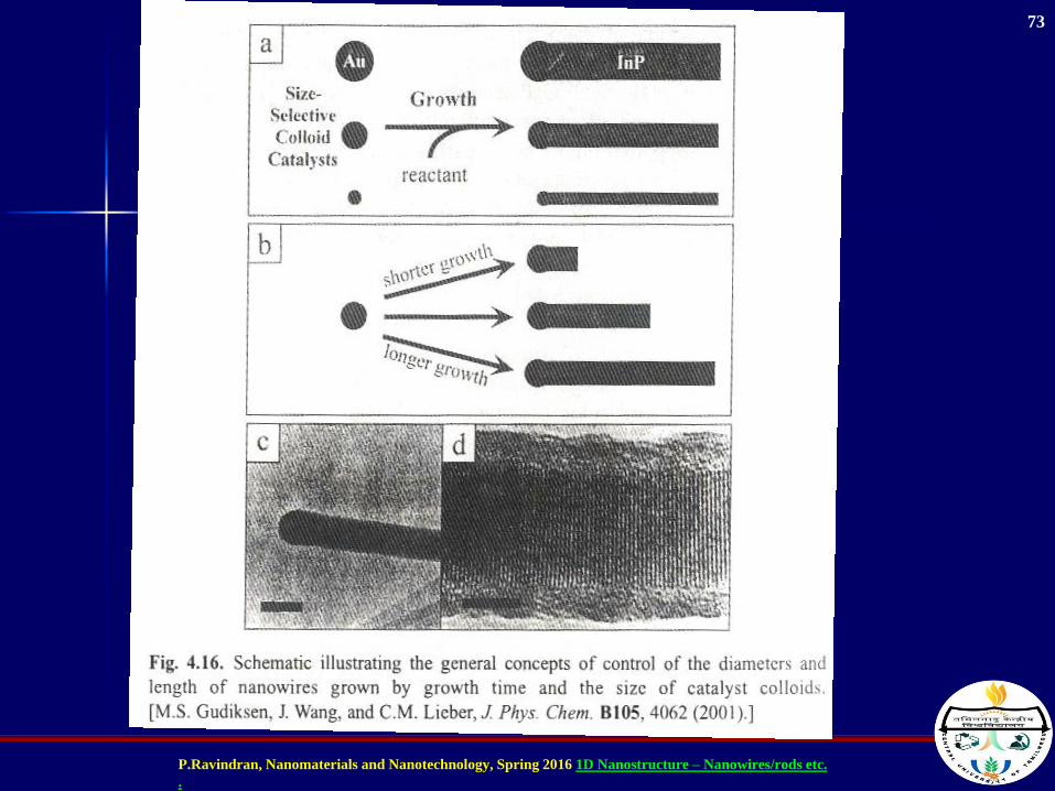
73
P.Ravindran, Nanomaterials and Nanotechnology, Spring 2016 1D Nanostructure – Nanowires/rods etc.
.
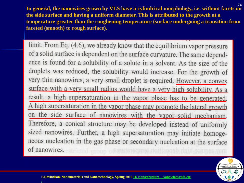
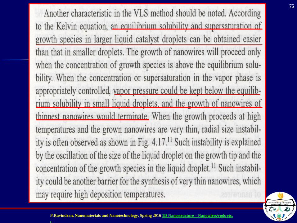
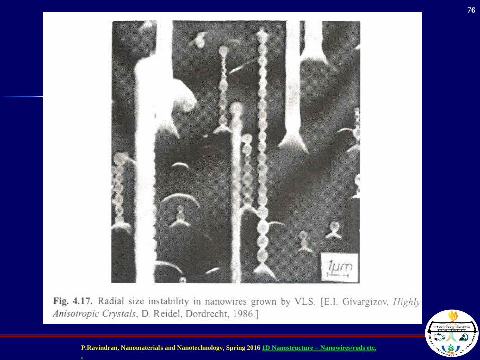
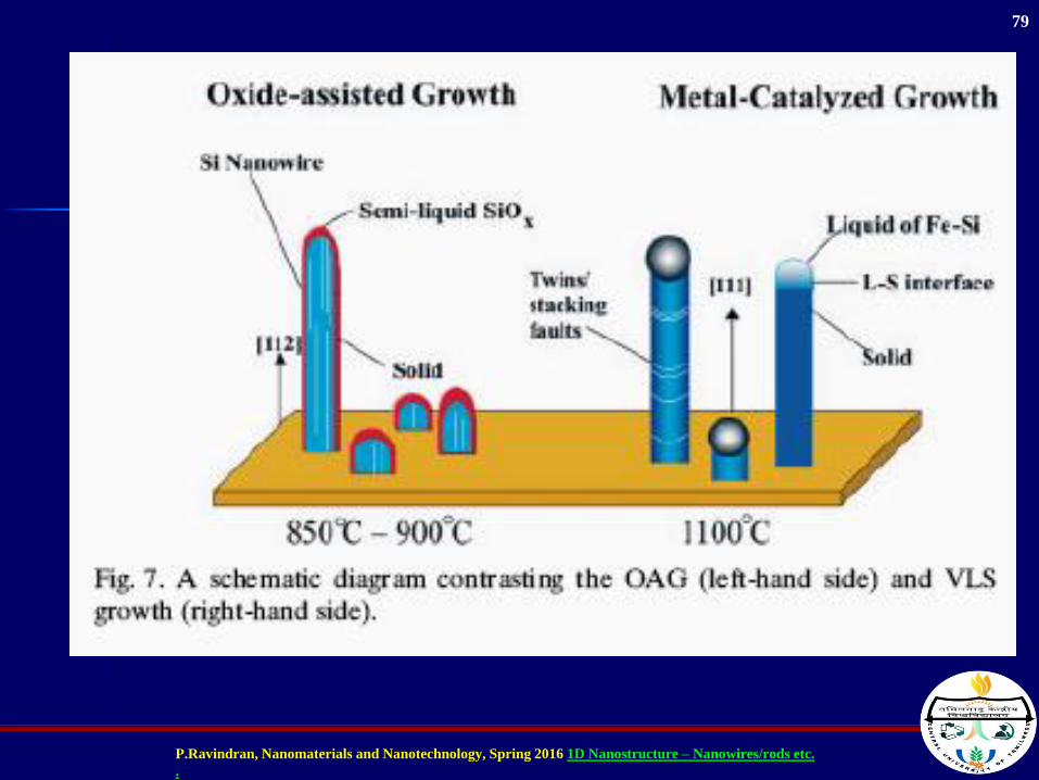
In general, the nanowires grown by VLS have a cylindrical morphology, i.e. without facets on
the side surface and having a uniform diameter. This is attributed to the growth at a
temperature greater than the roughening temperature (surface undergoing a transition from
faceted (smooth) to rough surface).
74
P.Ravindran, Nanomaterials and Nanotechnology, Spring 2016 1D Nanostructure – Nanowires/rods etc.
.
75
P.Ravindran, Nanomaterials and Nanotechnology, Spring 2016 1D Nanostructure – Nanowires/rods etc.
.
76
P.Ravindran, Nanomaterials and Nanotechnology, Spring 2016 1D Nanostructure – Nanowires/rods etc.
.
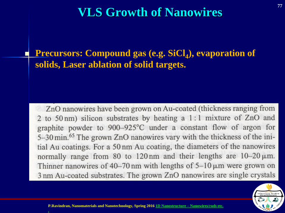
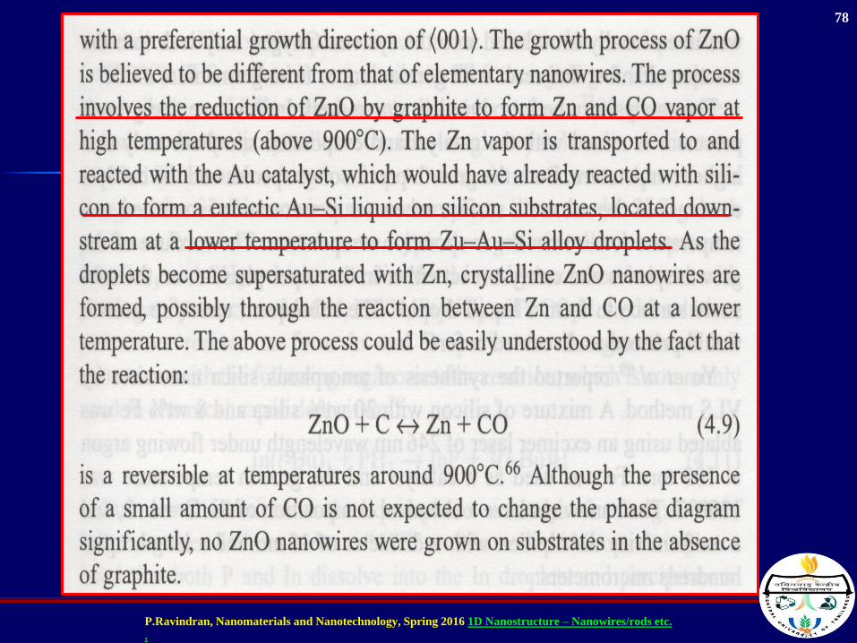
VLS Growth of Nanowires
Precursors: Compound gas (e.g. SiCl4), evaporation of
solids, Laser ablation of solid targets.
77
P.Ravindran, Nanomaterials and Nanotechnology, Spring 2016 1D Nanostructure – Nanowires/rods etc.
.
78
P.Ravindran, Nanomaterials and Nanotechnology, Spring 2016 1D Nanostructure – Nanowires/rods etc.
.
79
P.Ravindran, Nanomaterials and Nanotechnology, Spring 2016 1D Nanostructure – Nanowires/rods etc.
.
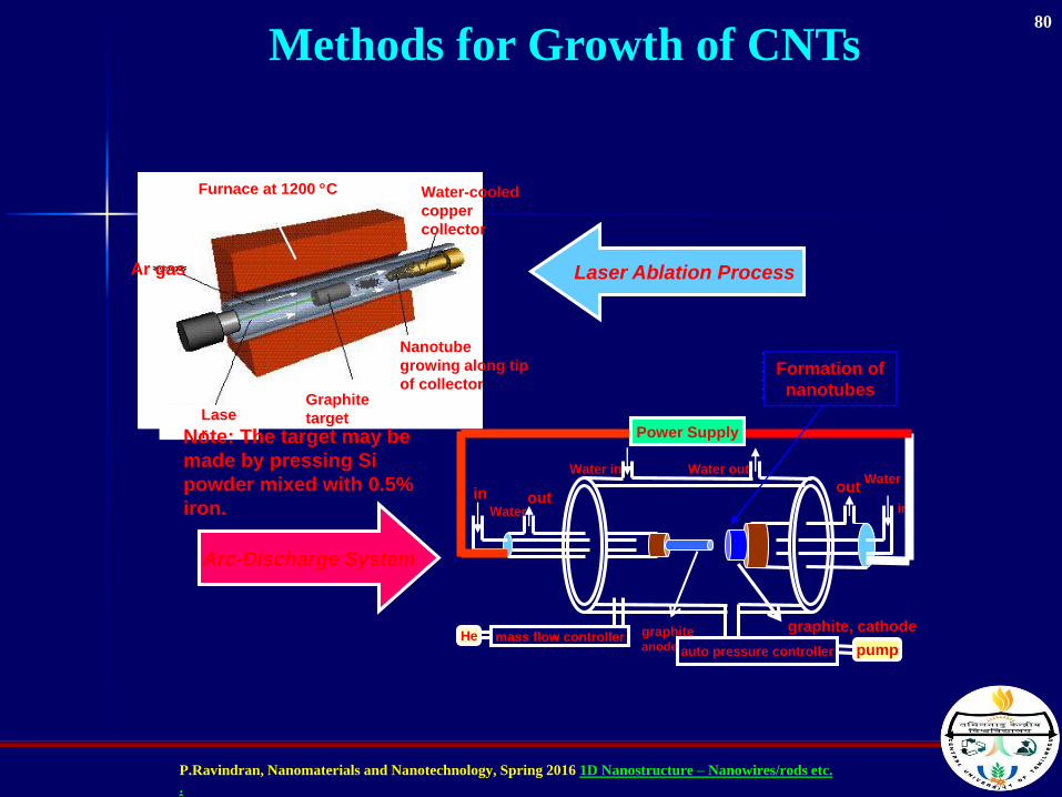
Methods for Growth of CNTs
Furnace at 1200 C
Ar gas
Graphite
targetLase
r
Water-cooled
copper
collector
Nanotube
growing along tip
of collector
Laser Ablation Process
Arc-Discharge System
Water
Water
inin out
out
graphite, cathodegraphite anode
Water in
Hepump
Water out
Power Supply
mass flow controllerauto pressure controller
Formation of
nanotubes
Note: The target may be
made by pressing Si
powder mixed with 0.5%
iron.
80
P.Ravindran, Nanomaterials and Nanotechnology, Spring 2016 1D Nanostructure – Nanowires/rods etc.
.
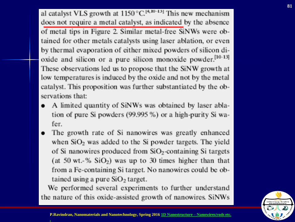
81
P.Ravindran, Nanomaterials and Nanotechnology, Spring 2016 1D Nanostructure – Nanowires/rods etc.
.
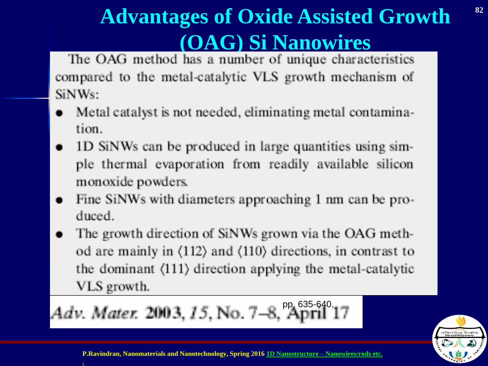
Advantages of Oxide Assisted Growth
(OAG) Si Nanowires
pp. 635-640.
82
P.Ravindran, Nanomaterials and Nanotechnology, Spring 2016 1D Nanostructure – Nanowires/rods etc.
.
83
P.Ravindran, Nanomaterials and Nanotechnology, Spring 2016 1D Nanostructure – Nanowires/rods etc.
.
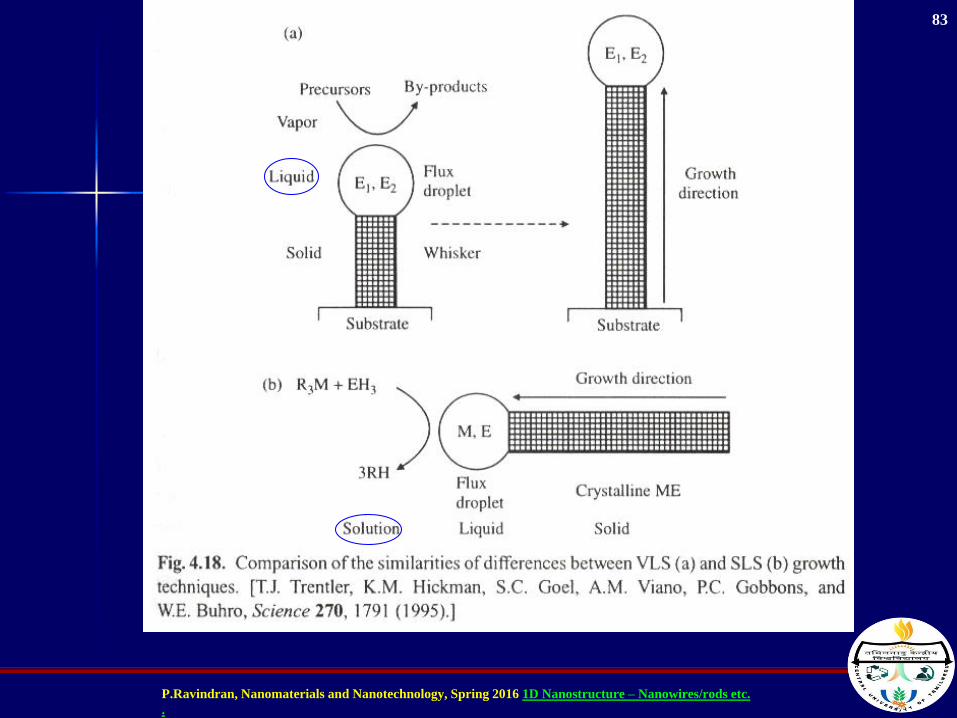
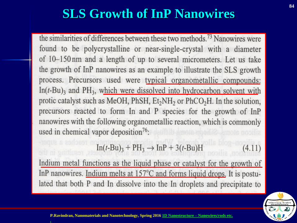
SLS Growth of InP Nanowires84
P.Ravindran, Nanomaterials and Nanotechnology, Spring 2016 1D Nanostructure – Nanowires/rods etc.
.
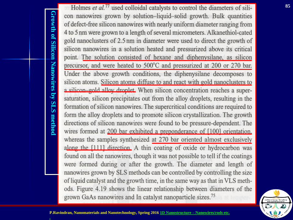
Gro
wth
of S
ilicon
Na
no
wires b
y S
LS
meth
od
85
P.Ravindran, Nanomaterials and Nanotechnology, Spring 2016 1D Nanostructure – Nanowires/rods etc.
.
86
P.Ravindran, Nanomaterials and Nanotechnology, Spring 2016 1D Nanostructure – Nanowires/rods etc.
.
87
P.Ravindran, Nanomaterials and Nanotechnology, Spring 2016 1D Nanostructure – Nanowires/rods etc.
.
Template-Based Synthesis-Electrochemical
Deposition
88
P.Ravindran, Nanomaterials and Nanotechnology, Spring 2016 1D Nanostructure – Nanowires/rods etc.
.
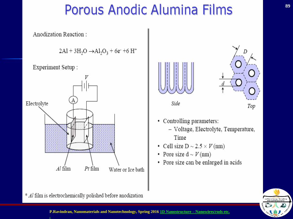
89
P.Ravindran, Nanomaterials and Nanotechnology, Spring 2016 1D Nanostructure – Nanowires/rods etc.
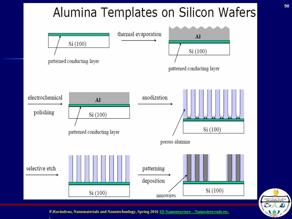
.
90
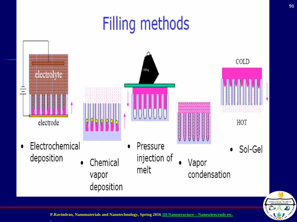
P.Ravindran, Nanomaterials and Nanotechnology, Spring 2016 1D Nanostructure – Nanowires/rods etc.
.
91
P.Ravindran, Nanomaterials and Nanotechnology, Spring 2016 1D Nanostructure – Nanowires/rods etc.
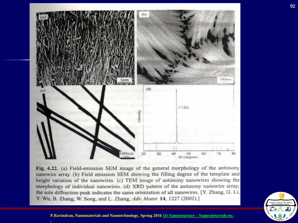
.
92
P.Ravindran, Nanomaterials and Nanotechnology, Spring 2016 1D Nanostructure – Nanowires/rods etc.
.
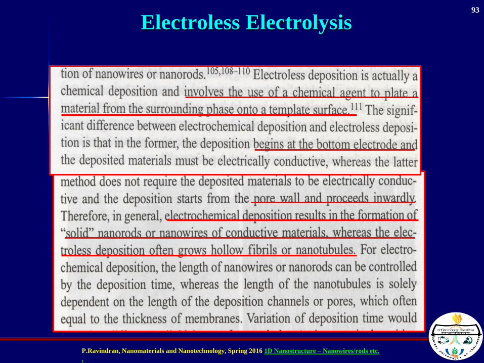
Electroless Electrolysis93
P.Ravindran, Nanomaterials and Nanotechnology, Spring 2016 1D Nanostructure – Nanowires/rods etc.
.
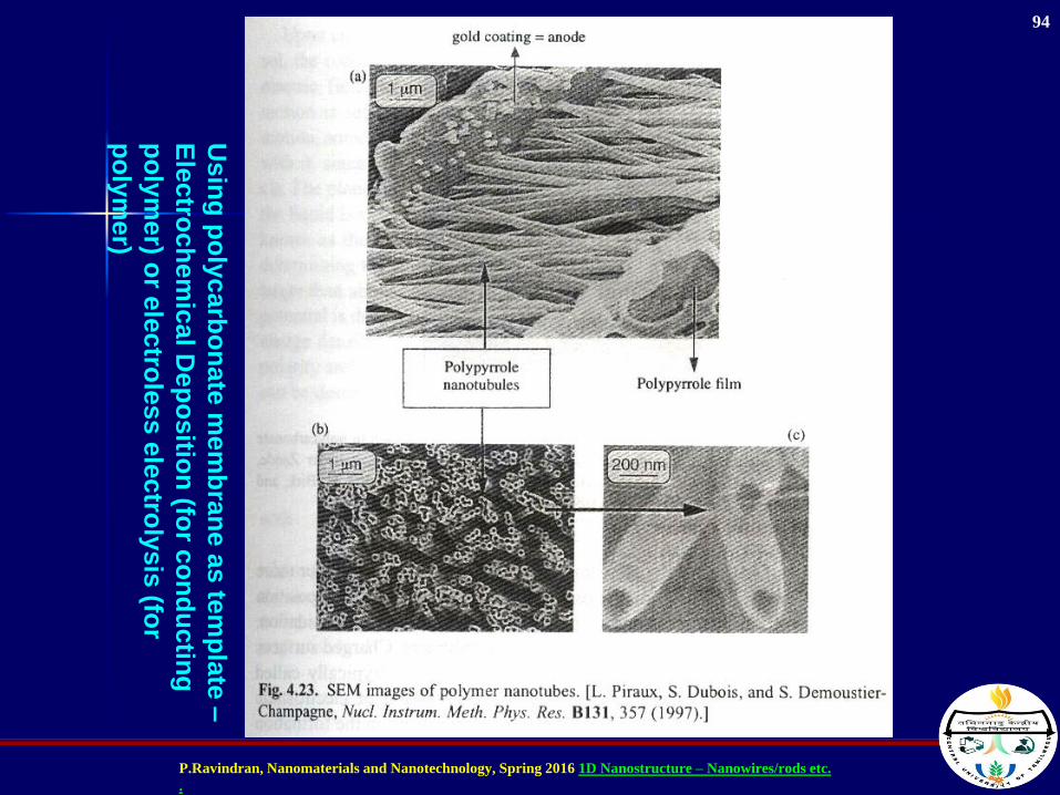
Usin
g p
oly
carb
on
ate
mem
bra
ne a
s te
mp
late
–
Ele
ctro
ch
em
ical D
ep
ositio
n (fo
r co
nd
uctin
g
po
lym
er) o
r ele
ctro
less
ele
ctro
lysis
(for
po
lym
er)
94
P.Ravindran, Nanomaterials and Nanotechnology, Spring 2016 1D Nanostructure – Nanowires/rods etc.
.
95
P.Ravindran, Nanomaterials and Nanotechnology, Spring 2016 1D Nanostructure – Nanowires/rods etc.
.
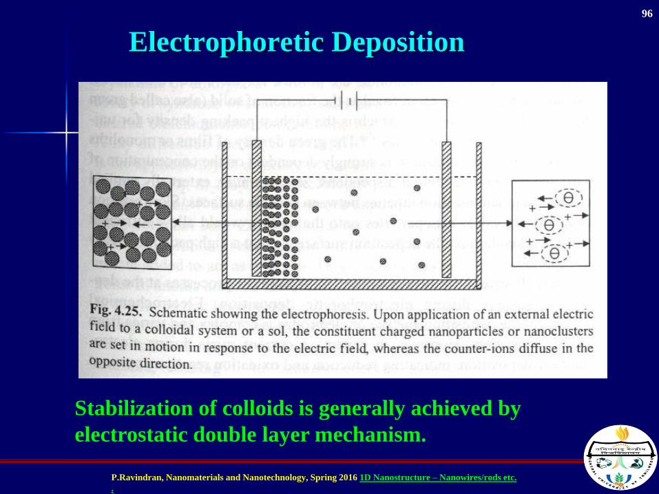
Electrophoretic Deposition
Stabilization of colloids is generally achieved by
electrostatic double layer mechanism.
96
P.Ravindran, Nanomaterials and Nanotechnology, Spring 2016 1D Nanostructure – Nanowires/rods etc.
.
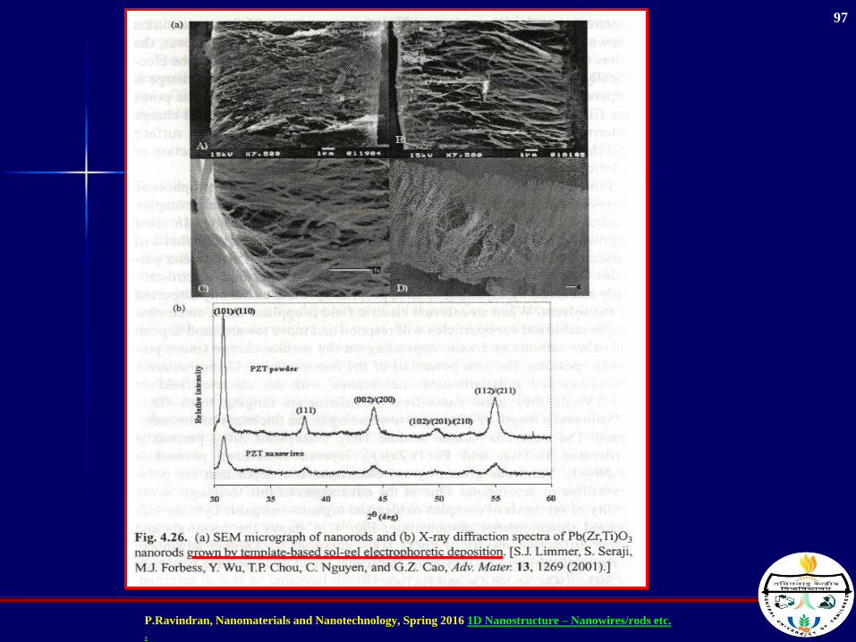
97
P.Ravindran, Nanomaterials and Nanotechnology, Spring 2016 1D Nanostructure – Nanowires/rods etc.
.
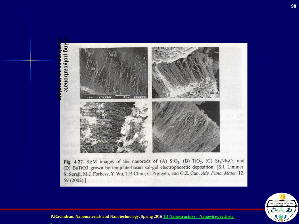
Us
ing
po
lyc
arb
on
ate
me
mb
ran
ce
as
tem
pla
te
98
P.Ravindran, Nanomaterials and Nanotechnology, Spring 2016 1D Nanostructure – Nanowires/rods etc.
.
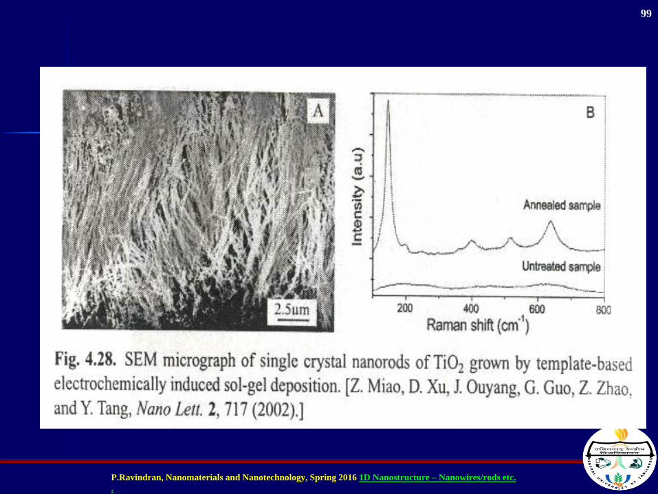
99
P.Ravindran, Nanomaterials and Nanotechnology, Spring 2016 1D Nanostructure – Nanowires/rods etc.
.
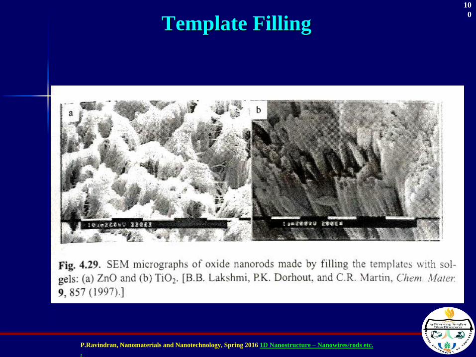
Template Filling10
0
P.Ravindran, Nanomaterials and Nanotechnology, Spring 2016 1D Nanostructure – Nanowires/rods etc.
.
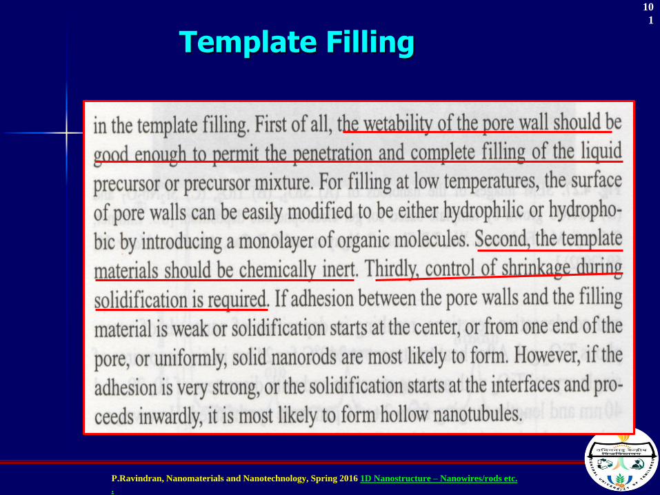
Template Filling
10
1
P.Ravindran, Nanomaterials and Nanotechnology, Spring 2016 1D Nanostructure – Nanowires/rods etc.
.
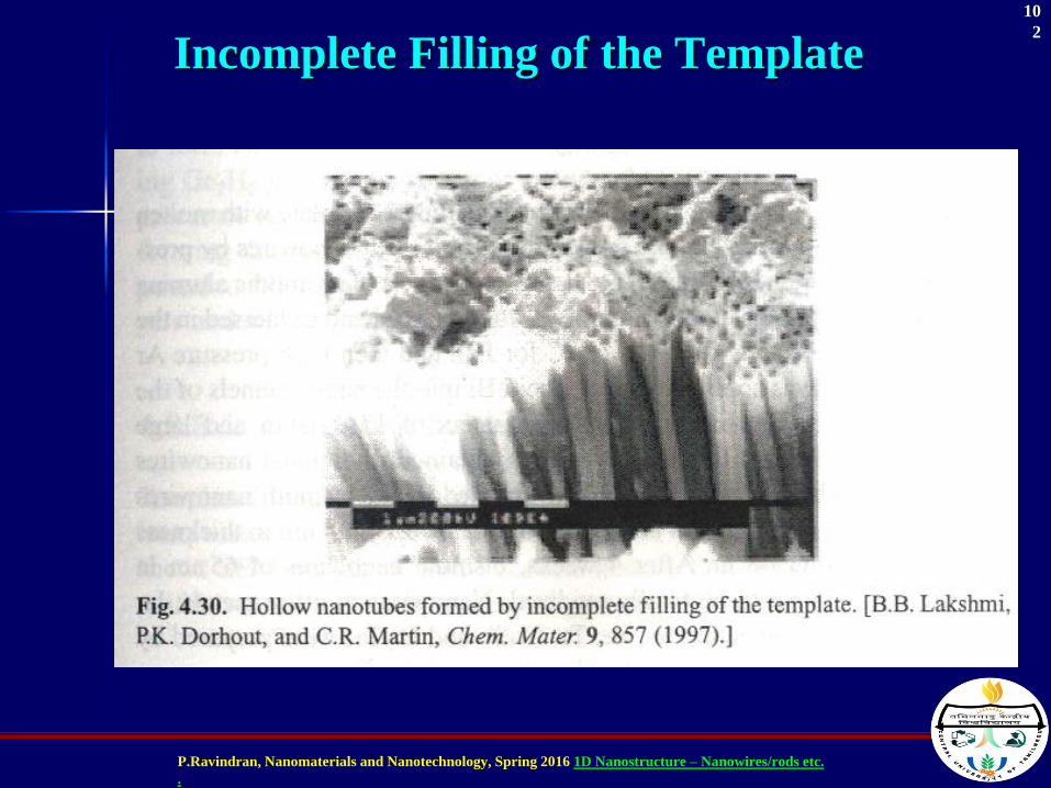
Incomplete Filling of the Template10
2
P.Ravindran, Nanomaterials and Nanotechnology, Spring 2016 1D Nanostructure – Nanowires/rods etc.
.
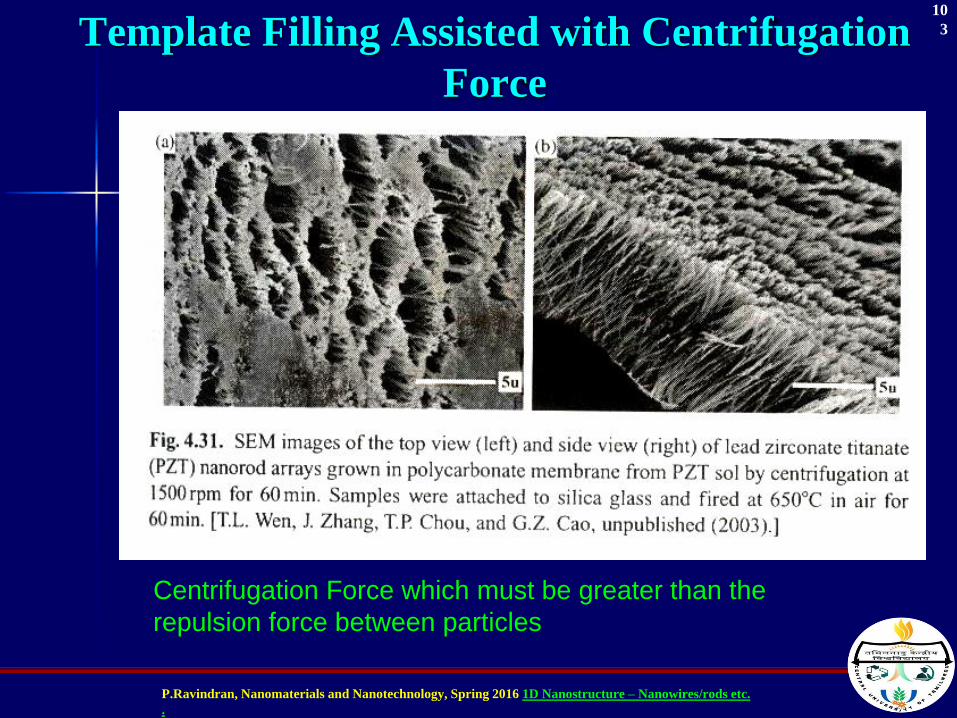
Template Filling Assisted with Centrifugation
Force
Centrifugation Force which must be greater than the
repulsion force between particles
10
3
P.Ravindran, Nanomaterials and Nanotechnology, Spring 2016 1D Nanostructure – Nanowires/rods etc.
.
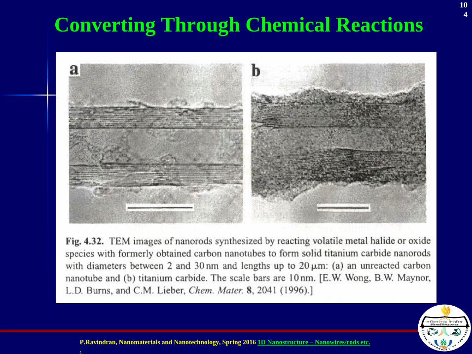
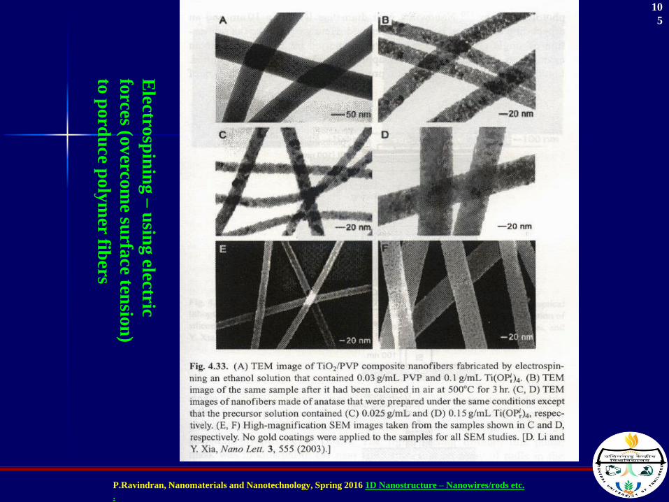
Converting Through Chemical Reactions
10
4
P.Ravindran, Nanomaterials and Nanotechnology, Spring 2016 1D Nanostructure – Nanowires/rods etc.