Programmable State-Variable Filter Design For a Feedback Systems Web-Based Laboratory by Rayal Johnson February 17, 2004 Advanced Undergraduate Project Massachusetts Institute of Technology Department of Electrical Engineering and Computer Science Supervisor: Dr. Kent Lundberg Abstract This document discusses the first installation of a weblab for a feedback systems class. A pro- grammable state-variable filter accessible through the web is designed and analyzed. The filter’s parameters such as the natural frequency and damping ratio are controlled through a web client and the effect of each parameter is analyzed and documented. 1
Transcript
Programmable State-Variable Filter Design For a
Feedback Systems Web-Based Laboratory
byRayal Johnson
February 17, 2004
Advanced Undergraduate Project
Massachusetts Institute of Technology
Department of Electrical Engineering and Computer Science
Supervisor: Dr. Kent Lundberg
Abstract
This document discusses the first installation of a weblab for a feedback systems class. A pro-grammable state-variable filter accessible through the web is designed and analyzed. The filter’sparameters such as the natural frequency and damping ratio are controlled through a web clientand the effect of each parameter is analyzed and documented.
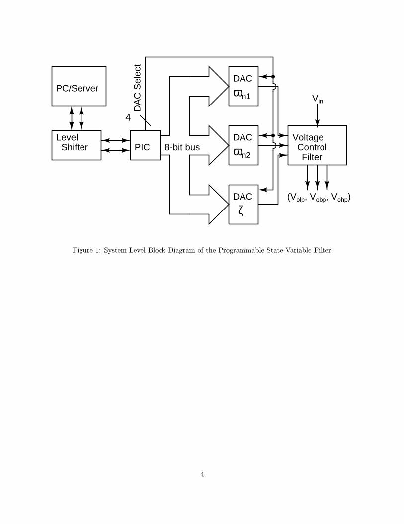
The programmable state-variable filter is the first part of a internet laboratory, also known as aweblab, for 6.302 (Feedback Systems). The weblab allows students access to real systems throughthe web much like the one used for 6.012 (Microelectronic Devices). The weblab allows students toperform experiments from their computer and eliminates the need to go to lab.
The types of experiments that are performed are frequency responses. To fully understandthe filter responses, these measurements must be made while changing filter characteristics suchas natural frequencies and damping ratio/quality factor. The natural frequencies determine thebandwith of the filter and the damping ratio/quality factor determine how much peaking occursat the corner frequency. In order to change these filter characteristics from a remote terminal, thecircuit representation of the filter needs to be adjusted by the server to which it is connected.
In order for the remote terminal to interface with the server, it must communicate with the serverthrough a scripting language. The server chosen for this project is the Apache Webserver, which isa free open source server that is easily configurable and extendable. The scripting language usedis the PHP scripting language, another open-source product. It is used because Apache supportsit and it has a powerful set a functions to create almost any type of application. One of thoseapplications is the full control of the server’s RS232 serial port which will be used in this projectto both send data to the circuit and to receive data from the circuit.
The overall weblab system consists of the PC/Server controlled by the remote client through thePHP scripting language, a level shifter, a microcontroller to interpret the server signals and setfilter characteristics, and the filter itself. A system level block diagram of the weblab system isshown in Figure 1. The DACs are latch free, so as long as the DAC select bits are set at the sametime as the data bits, they will work correctly. This is great for testing the DACs since there areno timing issues associated with writing to the DACs.
The level shifter changes RS232 logic (+12 and −12 volts) from the server to TTL logic (+5 and0 volts) which can be interpreted by the PIC microcontroller. The microcontroller uses the signalsfrom the server to determine the values to be sent to each digital to analog converter (DAC) over 8bits of data. The PIC processor has two input/output ports known as PORTA and PORTB, both8 bits wide. PORTA is used to DAC selection and PORTB is used to transfer the data.
3
VoltageControlFilter
8-bit busPICLevel
Shifter
PC/ServerDAC
DAC
DAC
Vin
DA
C S
elec
t
ζ
ωn1
ωn2
4
(Volp, Vobp, Vohp)
Figure 1: System Level Block Diagram of the Programmable State-Variable Filter
4
2 State Variable Filter: Theory
2.1 Overview
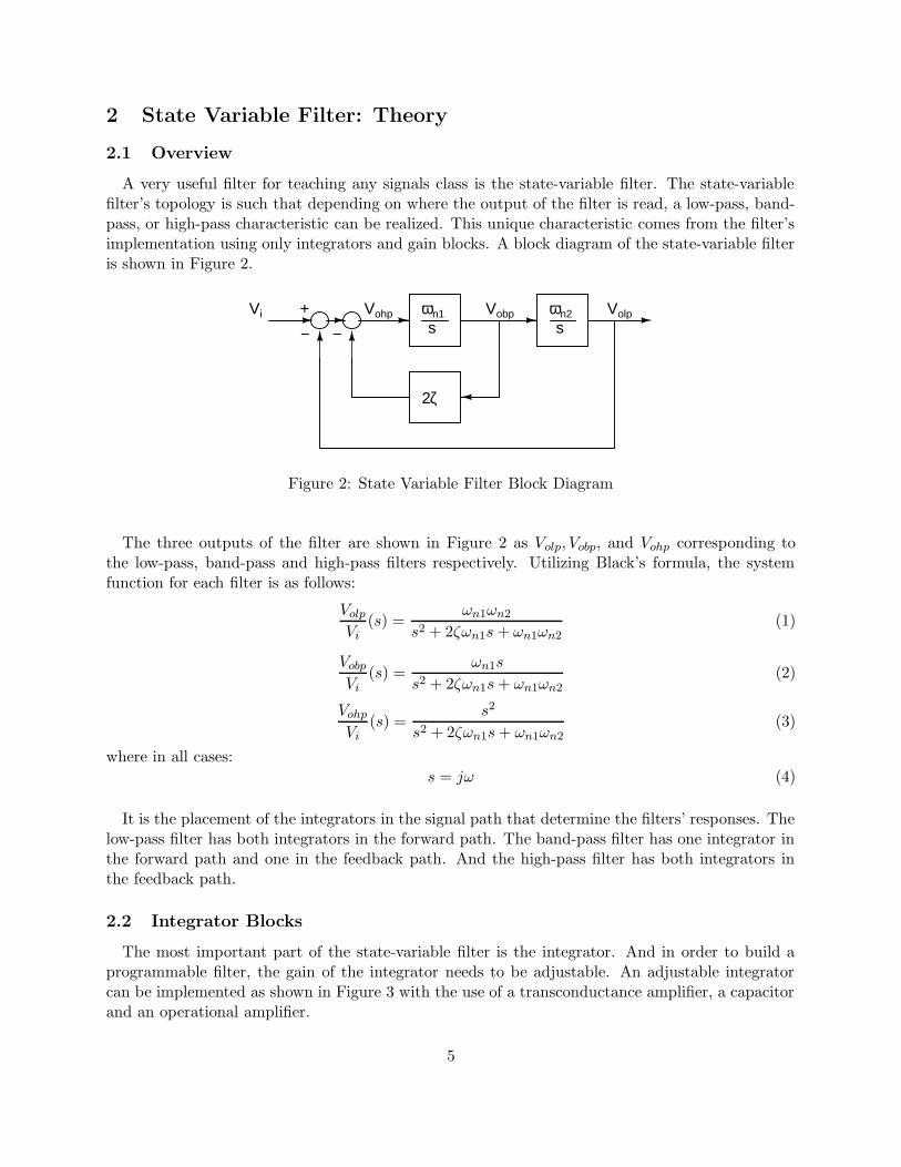
A very useful filter for teaching any signals class is the state-variable filter. The state-variablefilter’s topology is such that depending on where the output of the filter is read, a low-pass, band-pass, or high-pass characteristic can be realized. This unique characteristic comes from the filter’simplementation using only integrators and gain blocks. A block diagram of the state-variable filteris shown in Figure 2.
s s
2ζ
− −Vi + Vohp Vobp Volpωn1 ωn2
Figure 2: State Variable Filter Block Diagram
The three outputs of the filter are shown in Figure 2 as Volp, Vobp, and Vohp corresponding tothe low-pass, band-pass and high-pass filters respectively. Utilizing Black’s formula, the systemfunction for each filter is as follows:
Volp
Vi(s) =
ωn1ωn2
s2 + 2ζωn1s + ωn1ωn2(1)
Vobp
Vi
(s) =ωn1s
s2 + 2ζωn1s + ωn1ωn2(2)
Vohp
Vi(s) =
s2
s2 + 2ζωn1s + ωn1ωn2(3)
where in all cases:s = jω (4)
It is the placement of the integrators in the signal path that determine the filters’ responses. Thelow-pass filter has both integrators in the forward path. The band-pass filter has one integrator inthe forward path and one in the feedback path. And the high-pass filter has both integrators inthe feedback path.
2.2 Integrator Blocks
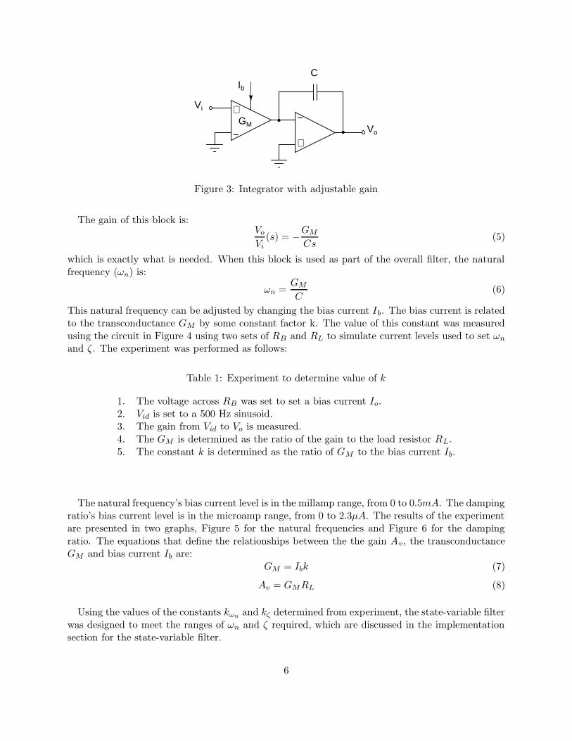
The most important part of the state-variable filter is the integrator. And in order to build aprogrammable filter, the gain of the integrator needs to be adjustable. An adjustable integratorcan be implemented as shown in Figure 3 with the use of a transconductance amplifier, a capacitorand an operational amplifier.
5
−
+−
+Vi
Vo
CIb
GM
Figure 3: Integrator with adjustable gain
The gain of this block is:Vo
Vi(s) = −
GM
Cs(5)
which is exactly what is needed. When this block is used as part of the overall filter, the naturalfrequency (ωn) is:
ωn =GM
C(6)
This natural frequency can be adjusted by changing the bias current Ib. The bias current is relatedto the transconductance GM by some constant factor k. The value of this constant was measuredusing the circuit in Figure 4 using two sets of RB and RL to simulate current levels used to set ωn
and ζ. The experiment was performed as follows:
Table 1: Experiment to determine value of k
1. The voltage across RB was set to set a bias current Io.2. Vid is set to a 500 Hz sinusoid.3. The gain from Vid to Vo is measured.4. The GM is determined as the ratio of the gain to the load resistor RL.5. The constant k is determined as the ratio of GM to the bias current Ib.
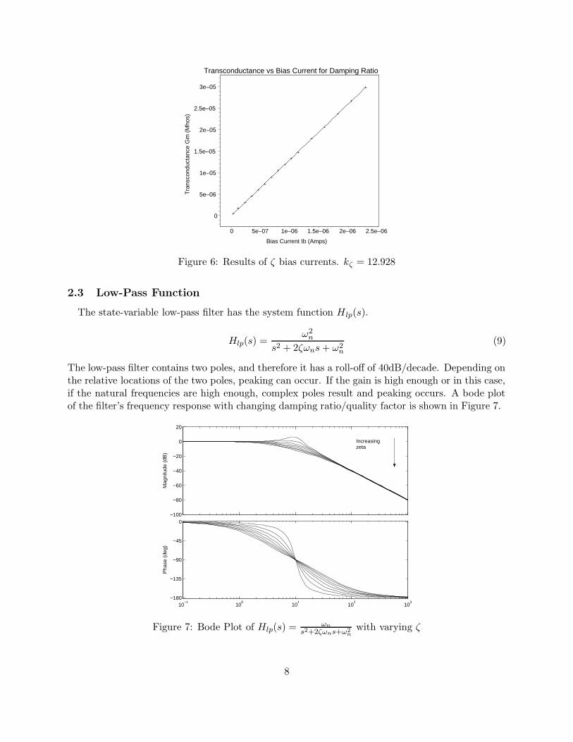
The natural frequency’s bias current level is in the millamp range, from 0 to 0.5mA. The dampingratio’s bias current level is in the microamp range, from 0 to 2.3µA. The results of the experimentare presented in two graphs, Figure 5 for the natural frequencies and Figure 6 for the dampingratio. The equations that define the relationships between the the gain Av, the transconductanceGM and bias current Ib are:
GM = Ibk (7)
Av = GMRL (8)
Using the values of the constants kωn and kζ determined from experiment, the state-variable filterwas designed to meet the ranges of ωn and ζ required, which are discussed in the implementationsection for the state-variable filter.
6
−
+VoVid
Ib
GM
−
+
+5V
RL
RB
+5V
Figure 4: Voltage Controlled Amplifier
The transconductance amplifier is slower than the operational amplifier, therefore contributingnon-negligible phase shifts correctable through compensation. 1
Transconductance vs Bias Current for Natural Frequency
0
0.002
0.004
0.006
0.008
Tra
nsco
nduc
tanc
e G
m (
Mho
s)
0 0.0001 0.0002 0.0003 0.0004 0.0005
Bias Current Ib (Amps)
Figure 5: Results of ωn bias currents. kωn = 15.029
1The use of a lead compensator can correct negative phase shifts by adding positive phase margin to the system.
7
Transconductance vs Bias Current for Damping Ratio
0
5e–06
1e–05
1.5e–05
2e–05
2.5e–05
3e–05
Tra
nsco
nduc
tanc
e G
m (
Mho
s)
0 5e–07 1e–06 1.5e–06 2e–06 2.5e–06
Bias Current Ib (Amps)
Figure 6: Results of ζ bias currents. kζ = 12.928
2.3 Low-Pass Function
The state-variable low-pass filter has the system function Hlp(s).
Hlp(s) =ω2
n
s2 + 2ζωns + ω2n
(9)
The low-pass filter contains two poles, and therefore it has a roll-off of 40dB/decade. Depending onthe relative locations of the two poles, peaking can occur. If the gain is high enough or in this case,if the natural frequencies are high enough, complex poles result and peaking occurs. A bode plotof the filter’s frequency response with changing damping ratio/quality factor is shown in Figure 7.
−100
−80
−60
−40
−20
0
20
Mag
nitu
de (
dB)
10−1
100
101
102
103
−180
−135
−90
−45
0
Pha
se (
deg)
Increasingzeta
Figure 7: Bode Plot of Hlp(s) = ωn
s2+2ζωns+ω2n
with varying ζ
8
The low-pass filter does just that, it lets low frequencies pass and attenuates frequencies higherthan its corner frequency. The corner frequency (ωn), where ωn = ωn1 = ωn2 in this bode plot is10 radians per second (krad/s), therefore, frequencies higher than 10 rad/s are attenuated.
2.4 Band-Pass Function
The state-variable band-pass filter has the system function Hbp(s).
Hbp(s) =ωns
s2 + 2ζωns + ω2n
(10)
The band-pass filter exhibits the peaking seen in the frequency response of the low-pass filter. Thischaracteristic comes from the fact that the filters have the same closed loop poles.
The band-pass filter’s frequency response explains what it does. The band-pass filter lets a bandof frequencies around its natural frequency, ωn = ωn1 = ωn2 is 10 rad/s in this case to pass,and attenuates frequencies much higher or much lower than the pass band. The band-pass filter’sfrequency response is shown in Figure 8.
−60
−50
−40
−30
−20
−10
0
10
Mag
nitu
de (
dB)
10−1
100
101
102
103
−90
−45
0
45
90
Pha
se (
deg)
Increasingzeta
Figure 8: Bode Plot of Hbp(s) = ωnss2+2ζωns+ω2
nwith varying ζ
2.5 High-Pass Function
The state-variable high-pass filter has the system function Hhp(s).
Hhp(s) =s2
s2 + 2ζωns + ω2n
(11)
The high-pass filter exhibits the peaking seen in the frequency response of the low-pass and theband-pass filters due to the fact that it too has the same closed loop poles. The band-pass filter’sfrequency response is shown in Figure 9. This filter lets high frequencies, those higher than its
9
−120
−100
−80
−60
−40
−20
0
20
Mag
nitu
de (
dB)
10−1
100
101
102
103
0
45
90
135
180P
hase
(de
g)
Increasing zeta
Figure 9: Bode Plot of Hhp(s) = s2
s2+2ζωns+ω2n
with varying ζ
natural frequency, ωn = ωn1 = ωn2 in this case, also 10 rad/s to pass and attenuates all otherfrequencies.
10
3 State Variable Filter: Implementation
3.1 Hardware
3.1.1 Filter
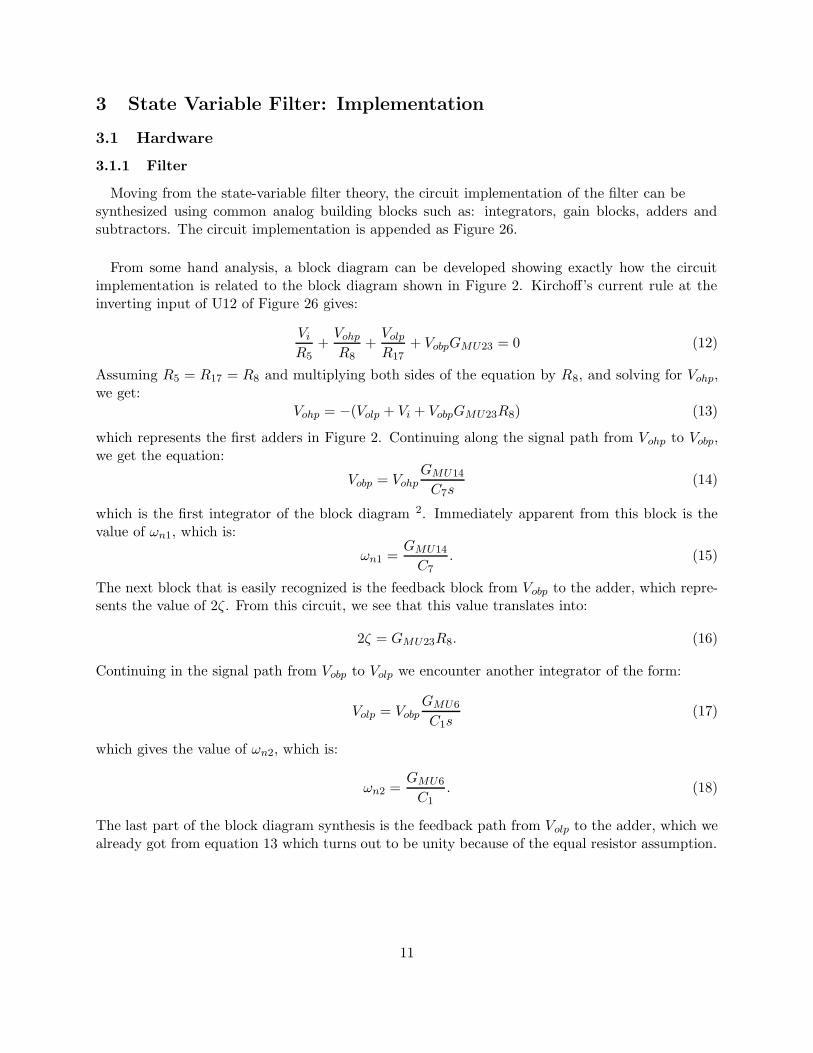
Moving from the state-variable filter theory, the circuit implementation of the filter can besynthesized using common analog building blocks such as: integrators, gain blocks, adders andsubtractors. The circuit implementation is appended as Figure 26.
From some hand analysis, a block diagram can be developed showing exactly how the circuitimplementation is related to the block diagram shown in Figure 2. Kirchoff’s current rule at theinverting input of U12 of Figure 26 gives:
Vi
R5+
Vohp
R8+
Volp
R17+ VobpGMU23 = 0 (12)
Assuming R5 = R17 = R8 and multiplying both sides of the equation by R8, and solving for Vohp,we get:
Vohp = −(Volp + Vi + VobpGMU23R8) (13)
which represents the first adders in Figure 2. Continuing along the signal path from Vohp to Vobp,we get the equation:
Vobp = Vohp
GMU14
C7s(14)
which is the first integrator of the block diagram 2. Immediately apparent from this block is thevalue of ωn1, which is:
ωn1 =GMU14
C7. (15)
The next block that is easily recognized is the feedback block from Vobp to the adder, which repre-sents the value of 2ζ. From this circuit, we see that this value translates into:
2ζ = GMU23R8. (16)
Continuing in the signal path from Vobp to Volp we encounter another integrator of the form:
Volp = Vobp
GMU6
C1s(17)
which gives the value of ωn2, which is:
ωn2 =GMU6
C1. (18)
The last part of the block diagram synthesis is the feedback path from Volp to the adder, which wealready got from equation 13 which turns out to be unity because of the equal resistor assumption.
The fact that the integrators have an noninverting topology is important to get negative feedbackas in the block diagram of Figure 2. The inversion of signals Volp, and Vobp of Equation 13 is whatgives the negative feedback, but since Vi is also inverted there is a phase shift of π
2 from the inputto the outputs. The resulting block diagram from this analysis is shown in Figure 10.
Now that it is confirmed that this circuit matches the block diagram of Figure 2, the parametersthat determine system dynamics can be analyzed. The system’s dynamics is adjustable throughthe transconductance amplifiers, and the specific relationships of ωn1, ωn2 and 2ζ to their controlvoltages are shown below:
ωn1 =kωn(Vdd − Vref1)
R6C7(19)
ωn2 =kωn(Vdd − Vref2)
R7C1(20)
2ζ =kζ(Vdd − Vref3)R8
R18(21)
The the last 3 equations were used to determine values for resistors and capacitors based on desiredranges of ωn1, ωn2, and ζ. The desired range of both ωn1 and ωn2 is 0 to 62.832 krad/s whichcorresponds to 10kHz. The desired range for ζ is from 0 to 2. Using the standard capacitor valueof 68nF, Vref−max of 5 volts, and VBE of 0.6 volts, the desired value for R6 and R7 is 15 kΩ, andthe desired value for R18 is 3.2 MΩ.
To understand where these equations originate, it is important to take a look at the circuit inFigure 11. This circuit is used to set the bias current for each transconductance amplifier pertainingto each system variable, i.e. ωn1, ωn2 and ζ. To see how the output bias current Io is related tothe reference voltage Vref , a feedback block diagram of this circuit is analyzed. The block diagramis shown in Figure 12.
The circuit in Figure 11 works through the use of two feedback loops to create a bias currentdependent only on the resistor Re and the reference voltage Vref . There is a major and minorfeedback loop in this circuit. The minor loop is provided by the emitter follower circuit and the
2Note, this integrator has a noninverting topology since it is the noninverting pin of the transconductance amplifier
that is grounded as opposed to the inverting pin.
12
−
+
Vdd
Vref
Ve
Vb
Io
Re
Figure 11: Circuit for Setting Bias Currents
major loop is provided by the operational amplifier. Using Black’s formula, the reference voltageVref is related to the output bias current Io by Equation 22.
Io
Vref
=
A(s)gm1+gmRe
1 + A(s)gmRe
1+gmRe
(22)
A(s) gm
Re
Re
__
++Vref Io
Ve Ve
Vb
Figure 12: Block Diagram for Bias Current Setting Circuit
The variables A(s), and gm represent the frequency-dependent gain of the operational amplifier,and the transconductance of the bipolar junction transistor respectively. Assuming Vref is changingslowly, the gain of the operational amplifier is at DC is 105 according to the TL082 datasheet andit is assumed that:
A(s)gmRe 1 + gmRe (23)
and the relationship between Vref and Io simplifies to:
Io
Vref
≈1
Re(24)
13
and therefore:
Io ≈Vref
Re(25)
One minor detail omitted when creating the block diagram of Figure 12 is that Vdd has an effecton the bias current. Vdd is assumed to be a small signal ground, and therefore omitted in the blockdiagram but the large signal bias current is dependent on this value and therefore the equationthat relates Vref and Io is more correctly:
Io =Vdd − Vref
Re
(26)
3.1.2 DAC-Filter Interface
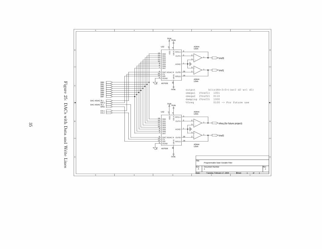
The bias currents that set the dynamics of the filter are set through the use of digital-to-analogconverters. Each DAC receives eight bits of data pertaining to the value of the filter’s characteristics,which are set by the user. The implementation of the DAC-Filter interface is shown in Figure 25.The data that is received by the DACs determines the reference voltages Vref1−3 derived fromEquations 19-21 which are reinterpreted here as:
Vref1 = Vdd −ωn1R6C7
kωn
(27)
Vref2 = Vdd −ωn1R7C1
kωn
(28)
Vref3 = Vdd −2ζR18
kζR8(29)
Future improvements on the programmable filter should use these equations in software to convertthe user’s inputs to eight bit values to set the reference voltages.
3.1.3 Computer-DAC Interface
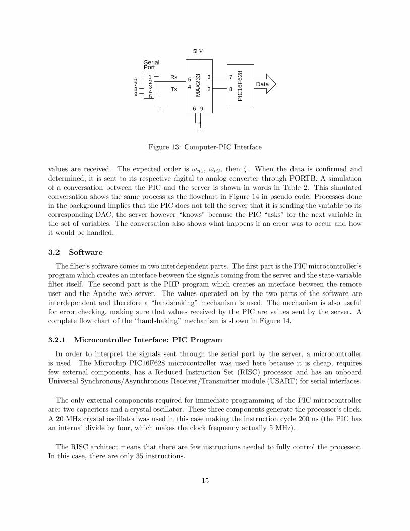
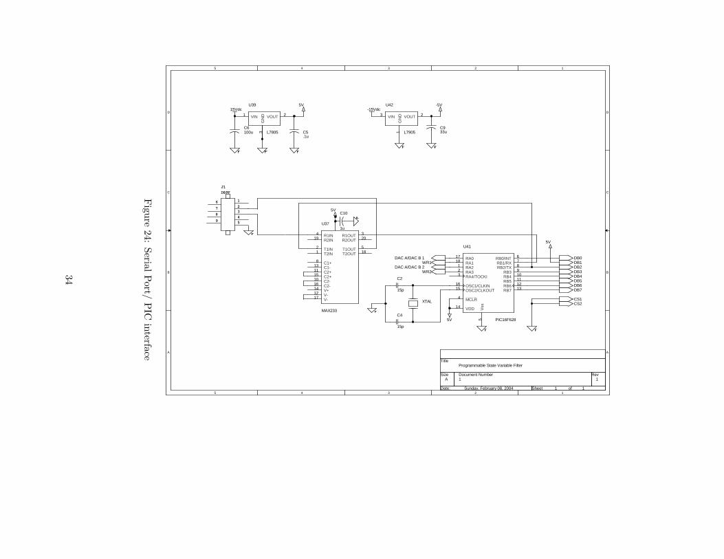
In order to use the signals from the RS232 interface, they need to be converted from RS232 logicto TTL logic. This means that the voltages need to be changed from +12 and −12 volts to 0 and+5 volts. This can done with the use of the Maxim 233 level shifter chip. The Maxim 232 takesRS232 logic and converts it to TTL for transmitting and vice versa for receiving. The only pinsneeded in this project are the ‘transmitted data’, ‘received data’ and ‘ground.’ With these threepins, a serial interface between the server and the PIC microcontoller is possible. The PIC has anonboard USART, with a receive and a transmit pin, therefore, the only configuration needed canbe done in software.
A diagram of the interface is shown in Figure 13. The protocol for checking if the right variableis sent is as follows. The PIC is initally set up to wait for a serially transmitted byte of data,meaning one bit after the other, least significant bit first. There are 8 bits of data, 1 stop bit andno parity. The processor then stores the variable and sends it back to the server. The server is thenexpected to send back to the PIC a ‘1’ if the data matches and a ‘0’ if it does not. The PIC thenchecks a counter to determine which variable was sent. The counter only updates when confirmed
14
12345
6789
Rx
Tx
54
MA
X23
3
+5V
6 9
PIC
16F
628
3
2
7
8Data
SerialPort
Figure 13: Computer-PIC Interface
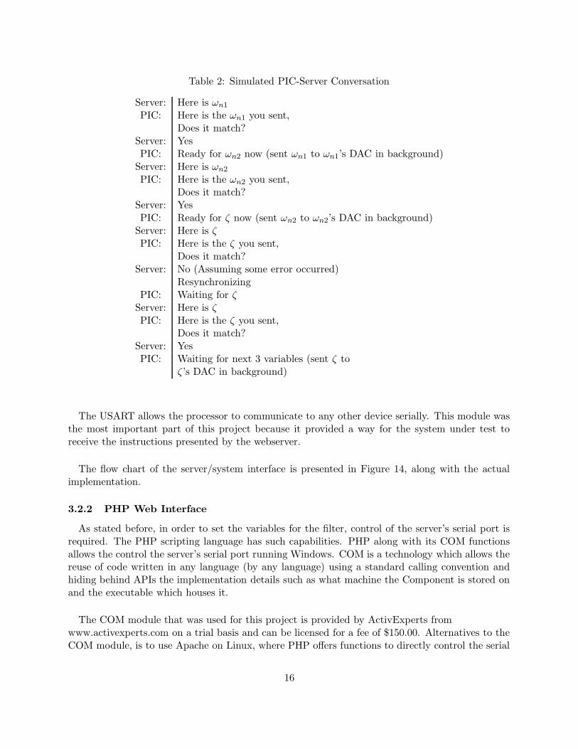
values are received. The expected order is ωn1, ωn2, then ζ. When the data is confirmed anddetermined, it is sent to its respective digital to analog converter through PORTB. A simulationof a conversation between the PIC and the server is shown in words in Table 2. This simulatedconversation shows the same process as the flowchart in Figure 14 in pseudo code. Processes donein the background implies that the PIC does not tell the server that it is sending the variable to itscorresponding DAC, the server however “knows” because the PIC “asks” for the next variable inthe set of variables. The conversation also shows what happens if an error was to occur and howit would be handled.
3.2 Software
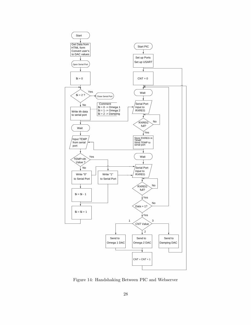
The filter’s software comes in two interdependent parts. The first part is the PIC microcontroller’sprogram which creates an interface between the signals coming from the server and the state-variablefilter itself. The second part is the PHP program which creates an interface between the remoteuser and the Apache web server. The values operated on by the two parts of the software areinterdependent and therefore a “handshaking” mechanism is used. The mechanism is also usefulfor error checking, making sure that values received by the PIC are values sent by the server. Acomplete flow chart of the “handshaking” mechanism is shown in Figure 14.
3.2.1 Microcontroller Interface: PIC Program
In order to interpret the signals sent through the serial port by the server, a microcontrolleris used. The Microchip PIC16F628 microcontroller was used here because it is cheap, requiresfew external components, has a Reduced Instruction Set (RISC) processor and has an onboardUniversal Synchronous/Asynchronous Receiver/Transmitter module (USART) for serial interfaces.
The only external components required for immediate programming of the PIC microcontrollerare: two capacitors and a crystal oscillator. These three components generate the processor’s clock.A 20 MHz crystal oscillator was used in this case making the instruction cycle 200 ns (the PIC hasan internal divide by four, which makes the clock frequency actually 5 MHz).
The RISC architect means that there are few instructions needed to fully control the processor.In this case, there are only 35 instructions.
15
Table 2: Simulated PIC-Server Conversation
Server: Here is ωn1
PIC: Here is the ωn1 you sent,Does it match?
Server: YesPIC: Ready for ωn2 now (sent ωn1 to ωn1’s DAC in background)
Server: Here is ωn2
PIC: Here is the ωn2 you sent,Does it match?
Server: YesPIC: Ready for ζ now (sent ωn2 to ωn2’s DAC in background)
Server: Here is ζPIC: Here is the ζ you sent,
Does it match?Server: No (Assuming some error occurred)
ResynchronizingPIC: Waiting for ζ
Server: Here is ζPIC: Here is the ζ you sent,
Does it match?Server: YesPIC: Waiting for next 3 variables (sent ζ to
ζ’s DAC in background)
The USART allows the processor to communicate to any other device serially. This module wasthe most important part of this project because it provided a way for the system under test toreceive the instructions presented by the webserver.
The flow chart of the server/system interface is presented in Figure 14, along with the actualimplementation.
3.2.2 PHP Web Interface
As stated before, in order to set the variables for the filter, control of the server’s serial port isrequired. The PHP scripting language has such capabilities. PHP along with its COM functionsallows the control the server’s serial port running Windows. COM is a technology which allows thereuse of code written in any language (by any language) using a standard calling convention andhiding behind APIs the implementation details such as what machine the Component is stored onand the executable which houses it.
The COM module that was used for this project is provided by ActivExperts fromwww.activexperts.com on a trial basis and can be licensed for a fee of $150.00. Alternatives to theCOM module, is to use Apache on Linux, where PHP offers functions to directly control the serial
16
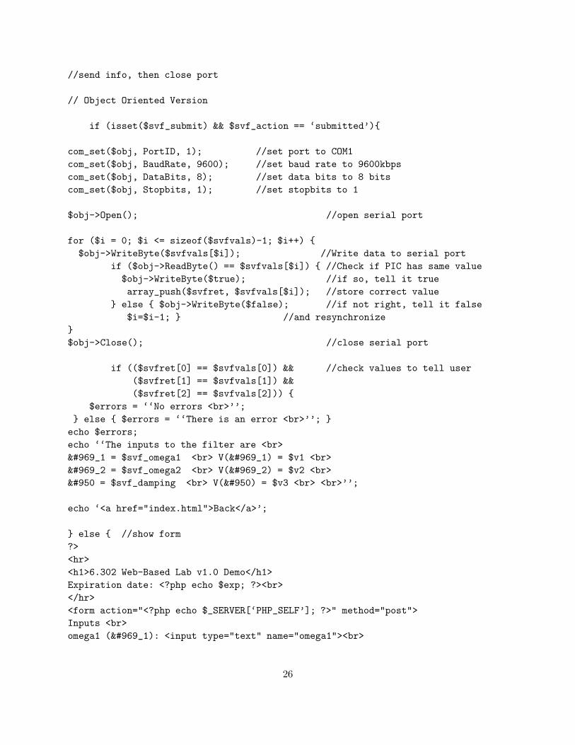
port, or write a Dynamic Linked-Library (.dll) file so that a windows based server can control theserial port. The PHP code that makes use of this module is shown in Appendix B. The code takesthe user values entered in a form and prepares them for transmission to the webserver and to itsserial port, which is later on interpreted by the PIC processor for setting filter values. There isa ”hand-shaking” mechanism implemented such that PHP and the microcontroller have the samevalues presented by the user.
17
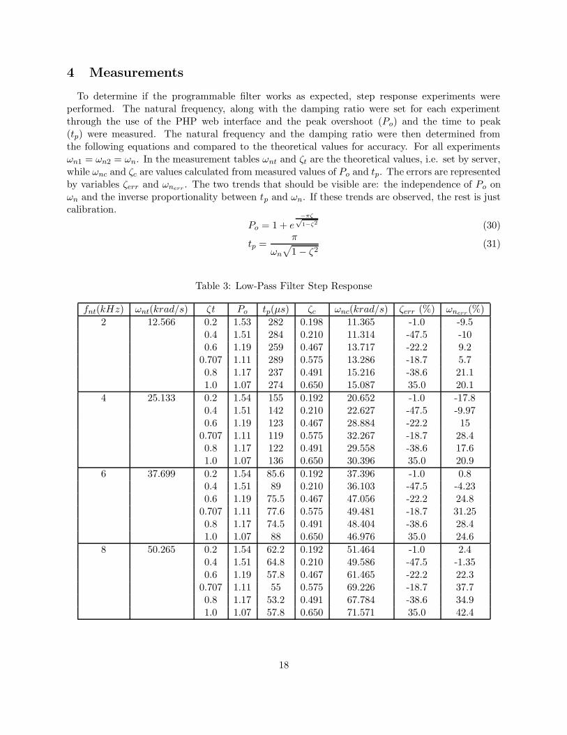
4 Measurements
To determine if the programmable filter works as expected, step response experiments wereperformed. The natural frequency, along with the damping ratio were set for each experimentthrough the use of the PHP web interface and the peak overshoot (Po) and the time to peak(tp) were measured. The natural frequency and the damping ratio were then determined fromthe following equations and compared to the theoretical values for accuracy. For all experimentsωn1 = ωn2 = ωn. In the measurement tables ωnt and ζt are the theoretical values, i.e. set by server,while ωnc and ζc are values calculated from measured values of Po and tp. The errors are representedby variables ζerr and ωnerr . The two trends that should be visible are: the independence of Po onωn and the inverse proportionality between tp and ωn. If these trends are observed, the rest is justcalibration.
Po = 1 + e−πζ
√
1−ζ2 (30)
tp =π
ωn
√
1 − ζ2(31)
Table 3: Low-Pass Filter Step Response
fnt(kHz) ωnt(krad/s) ζt Po tp(µs) ζc ωnc(krad/s) ζerr (%) ωnerr(%)
From the measurements table, it is clear that the two required trends are present, but asidefrom that, the measurements seem to contain a large amount of error within the center values of ζ.Reasons for this could be a nonlinear GM of the transconductance amplifiers when they are usedin the overall filter, measurement errors, calibration techniques, i.e. rounding the final value to besent to the DAC to rid the data of leading decimals. This rounding function under PHP will roundboth 4.5 and 4.99 up to 5. Another problem discovered by the author was the value of kωn andkζ . The values determined from the test circuit and the values observed in the circuit were notconsistent. The values were adjusted on the server side until an expected response was observed,but then, this was not the case at all points of measurement as apparent from the low error inboth variables at ζ = 0.2. There were no other problems other than calibration errors, because thesignals overall appeared to match the step reponses in Figures 15-17
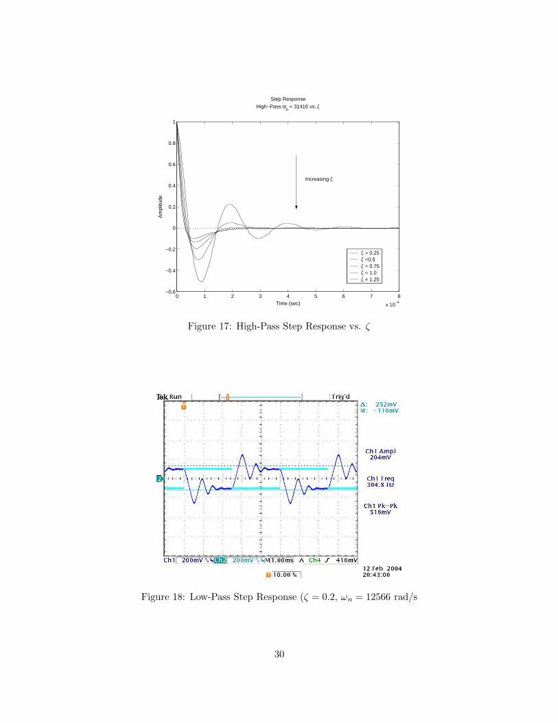
Some of the step response signals for each output are shown in Figures 18-23. These Figureswere taken at a time when ζ was calibrated well by ωn was not.
19
5 Future Work
Future work to be completed for the weblab project includes the construction of more sys-tems/filters and the implementation of a graphical user interface (GUI) to control the experimentsand to gather data from those experiments. More robust calibration techiques need also to beimplemented for this specific filter, most likely could be done in the software on the server side.
Other work includes the construction of more filters/systems for experimentation. Althougha state-variable filter is a great example of a low-pass, band-pass and high-pass filter, a moreextensive set of filters are required for feedback systems. Filters that are more specific to 6.302 arethe lag, lead, and the dominant pole compensators/filters. These filters demonstrate the benefits offeedback to achieve more desirable system dynamics than those of the open-loop or uncompensatedsystem.
20
6 Conclusion
The programmable state-variable filter is a good start to the installation of a feedback systemsweblab, but the first version is not perfect and can be improved upon. For a version 2, a PIC withthe USART on a separate port from the data port should be chosen. The PIC16F628 was chosenbecause it had 2 byte sized ports, an onboard USART, and is inexpensive. The replacement shouldhave an onboard USART separate from the data ports, in addition to the requirements above.
The shared port of the PIC16F628 causes a 2-bit error because the receive pin is not available tosend data to the DACs since it is configured as an input for the USART. The receive pin thereforeeither sits at either 5 volts or ground depending on the output from the level shifter, and cannotbe connected to any other potential. A diagram of the connections between the PIC and the levelshifter is shown in Figure 25. Since the receive pin cannot be used as an output, data bit DB1 isconnected to 5 volts in this case.
The 2 bit error might be acceptable for a first version of the filter but future filters/systems mayrequire higher precision for acceptable use. In its present state, the DAC is referenced to 5 voltstherefore a 2 bit error represents an error in voltage of just:
Verror =2
2565 = 0.039mV (32)
which represents an error of 981 rad/s in ωn and 0.03 in ζ.
Although the two bits of error is important, this was not the greatest of problems. The greatestproblem is the calibration of the filter which was discussed before. For although the two bit errorcaused a maximum of 5.7% error, it does not explain the large 20 to 48% errors observed in themeasurements.


![Plus 2-AxisPanel EtherCAT BE2 RoHS[IN3,4,12,13] Digital, non-isolated, programmable as single-ended or differential pairs, 100 ns RC filter, 12 Vdc max, 10 kΩ programmable pull-up/down](https://static.documents.pub/doc/80x56/60b16e48a21c90011033e8b8/plus-2-axispanel-ethercat-be2-in341213-digital-non-isolated-programmable.jpg)