Programming TMS320x28xx and 28xxx Peripherals inC/C++
Lori Heustess .................................................................................................................. AEC C2000
ABSTRACTThis application report explores a hardware abstraction layer implementation to make C/C++ coding easieron C28x™ devices. This method is compared to traditional #define macros and topics of code efficiencyand special case registers are also addressed.
Contents1 Introduction .................................................................................................................. 12 Traditional #define Approach .............................................................................................. 33 Bit Field and Register-File Structure Approach ......................................................................... 54 Bit Field and Register-File Structure Advantages ..................................................................... 115 Code Size and Performance Using Bit Fields ......................................................................... 126 Read-Modify-Write Considerations When Using Bit Fields .......................................................... 167 A Special Case: eCAN Control Registers .............................................................................. 218 References ................................................................................................................. 22
The TMS320x28xx and TMS328x28xxx are members of the C2000™ generation for embedded controlapplications. To facilitate writing efficient and easy-to-maintain embedded C/C++ code on these devices,Texas Instruments provides a hardware abstraction layer method for accessing memory-mappedperipheral registers. This method is the bit field and register-file structure approach. This application reportexplains the implementation of this hardware abstraction layer and compares it to traditional #definemacros. Topics of code efficiency and special case registers are also addressed.
C28x, C2000 are trademarks of Texas Instruments.Code Composer Studio is a trademark of Texas Instruments Inc..All other trademarks are the property of their respective owners.
1«SPRAA85B–September 2009 Programming TMS320x28xx and 28xxx Peripherals in C/C++Submit Documentation Feedback
The hardware abstraction layer discussed in this application report has been implemented as a collectionof C/C++ header files available for download from Texas Instruments:
• Piccolo Series Microcontrollers– 2802x C/C++ Header Files and Peripheral Examples (SPRC832)– 2803x C/C++ Header Files and Peripheral Examples (SPRC892)
• Delfino (Floating-Point) Series– C2833x/C2823x C/C++ Header Files and Peripheral Examples (SPRC530)– C2834x C/C++ Header Files and Peripheral Examples (SPRC892)
• Other Fixed-Point C28x Microcontrollers– C2833x/C2823x C/C++ Header Files and Peripheral Examples (SPRC530)– C281x C/C++ Header Files and Peripheral Examples (SPRC097)– C280x, C2801x C/C++ Header Files and Peripheral Examples (SPRC191)– C2804x C/C++ Header Files and Peripheral Examples (SPRC324)
Depending on your current needs, the software included in these downloads are learning tools or thebasis for a development platform.
• Learning Tool:The C/C++ Header Files and Peripheral Examples include several example Code Composer Studio™projects. These examples explain the steps required to initialize the device and utilize on-chipperipherals. The examples can be copied and modified to quickly experiment with peripheralconfigurations.
• Development Platform:The header files can be incorporated into a project as a hardware abstraction layer for accessingon-chip peripherals using C or C++ code. You can also pick and choose functions as needed anddiscard the rest.
This application report does not provide a tutorial on C, C++, C28xx assembly, or emulation tools. Youshould have a basic understanding of C code and the ability to load and run code using Code ComposerStudio. While knowledge of C28xx assembly is not required to understand the hardware abstraction layer,it is useful to understand the code optimization and read-modify-write sections. If you have assemblyinstruction-related questions, see the TMS320C28x CPU and Instruction Set Reference Guide(SPRU430).
Examples are based on the following software versions:
• C/C++ Header Files and Peripheral Examples refers to any of the header file packages: C281x C/C++Header Files and Peripheral Examples (SPRC097) , C280x C2801x C/C++ Header Files andPeripheral Examples (SPRC191) or C2804x C/C++ Header Files and Peripheral Examples (SPRC324)
• TMS320x280x and 280x refer to all devices in the TMS320x280x and TMS320x2801x family and theUCD9501. For example: TMS320F2801, TMS320F2806, TMS320F2808, TMS320F28015 andTMS320F28016.
• TMS320x2804x and 2804x refers all devices in the TMS320x2804x family. For example, theTMS320F28044.
• TMS320x281x and 281x refer to all devices in the TMS320x281x family. For example: TMS320F2810,TMS320F2811, and TMS320F2812, TMS320C2810, and so forth.
• C28x refers to the TMS320C28x CPU; this CPU is used on all of the above DSPs.
2 Programming TMS320x28xx and 28xxx Peripherals in C/C++ «SPRAA85B–September 2009Submit Documentation Feedback
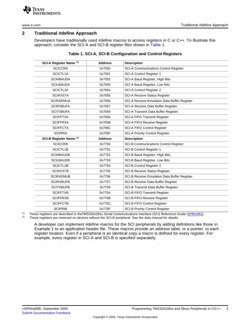
Developers have traditionally used #define macros to access registers in C or C++. To illustrate thisapproach, consider the SCI-A and SCI-B register files shown in Table 1.
Table 1. SCI-A, SCI-B Configuration and Control Registers
SCI-A Register Name (1) Address Description
SCICCRA 0x7050 SCI-A Communications Control Register
SCICTL1A 0x7051 SCI-A Control Register 1
SCIHBAUDA 0x7052 SCI-A Baud Register, High Bits
SCILBAUDA 0x7053 SCI-A Baud Register, Low Bits
SCICTL2A 0x7054 SCI-A Control Register 2
SCIRXSTA 0x7055 SCI-A Receive Status Register
SCIRXEMUA 0x7056 SCI-A Receive Emulation Data Buffer Register
SCIRXBUFA 0x7057 SCI-A Receive Data Buffer Register
SCITXBUFA 0x7059 SCI-A Transmit Data Buffer Register
SCIFFTXA 0x705A SCI-A FIFO Transmit Register
SCIFFRXA 0x705B SCI-A FIFO Receive Register
SCIFFCTA 0x705C SCI-A FIFO Control Register
SCIPRIA 0x705F SCI-A Priority Control Register
SCI-B Register Name (2) Address Description
SCICCRB 0x7750 SCI-B Communications Control Register
SCICTL1B 0x7751 SCI-B Control Register 1
SCIHBAUDB 0x7752 SCI-B Baud Register, High Bits
SCILBAUDB 0x7753 SCI-B Baud Register, Low Bits
SCICTL2B 0x7754 SCI-B Control Register 2
SCIRXSTB 0x7755 SCI-B Receive Status Register
SCIRXEMUB 0x7756 SCI-B Receive Emulation Data Buffer Register
SCIRXBUFB 0x7757 SCI-B Receive Data Buffer Register
SCITXBUFB 0x7759 SCI-B Transmit Data Buffer Register
SCIFFTXB 0x775A SCI-B FIFO Transmit Register
SCIFFRXB 0x775B SCI-B FIFO Receive Register
SCIFFCTB 0x775C SCI-B FIFO Control Register
SCIPRIB 0x775F SCI-B Priority Control Register(1) These registers are described in theTMS320x281x Serial Communications Interface (SCI) Reference Guide (SPRU051).(2) These registers are reserved on devices without the SCI-B peripheral. See the data manual for details.
A developer can implement #define macros for the SCI peripherals by adding definitions like those inExample 1 to an application header file. These macros provide an address label, or a pointer, to eachregister location. Even if a peripheral is an identical copy a macro is defined for every register. Forexample, every register in SCI-A and SCI-B is specified separately.
3«SPRAA85B–September 2009 Programming TMS320x28xx and 28xxx Peripherals in C/C++Submit Documentation Feedback
/********************************************************************* Traditional header file********************************************************************/
#define Uint16 unsigned int#define Uint32 unsigned long
Some advantages of traditional #define macros are:
• Macros are simple, fast, and easy to type.• Variable names exactly match register names; variable names are easy to remember.
Disadvantages to traditional #define macros include the following:
• Bit fields are not easily accessible; you must generate masks to manipulate individual bits.• You cannot easily display bit fields within the Code Composer Studio watch window.• Macros do not take advantage of Code Composer Studio's auto-completion feature.• Macros do not benefit from duplicate peripheral reuse.
4 Programming TMS320x28xx and 28xxx Peripherals in C/C++ «SPRAA85B–September 2009Submit Documentation Feedback
www.ti.com Bit Field and Register-File Structure Approach
3 Bit Field and Register-File Structure Approach
Instead of accessing registers using #define macros, it is more flexible and efficient to use a bit field andregister-file structure approach.
• Register-File Structures:A register file is the collection of registers belonging to a peripheral. These registers are groupedtogether in C/C++ as members of a structure; this is called a register-file structure. Each register-filestructure is mapped in memory directly over the peripheral registers at compile time. This mappingallows the compiler to efficiently access the registers using the CPU's data page pointer (DP).
• Bit Field Definitions:Bit fields can be used to assign a name and width to each functional field within a register. Registersdefined in terms of bit fields allow the compiler to manipulate single elements within a register. Forexample, a flag can be read by referencing the bit field name corresponding to that flag.
The remainder of this section describes a register-file structure with bit-field implementation for the SCIperipherals. This process consists of the following steps:
1. Create a simple SCI register-file structure variable type; this implementation does not include bit fields.2. Create a variable of this new type for each of the SCI instances.3. Map the register-file structure variables to the first address of the registers using the linker.4. Add bit-field definitions for select SCI registers.5. Add union definitions to provide access to either bit fields or the entire register.6. Rewrite the register-file structure type to include the bit-field and union definitions.
In the C/C++ Header Files and Peripheral Examples, the register-file structures and bit fields have beenimplemented for all peripherals on the TMS320x28xx and TMS320x28xxx devicess.
3.1 Defining A Register-File Structure
Example 1 showed a hardware abstraction implementation using #define macros. In this section, theimplementation is changed to a simple register file structure. Table 2 lists the registers that belong to theSCI peripheral. This register file is identical for each instance of the SCI, i.e., SCI-A and SCI-B.
Table 2. SCI-A and SCI-B Common Register File
Name Size Address Offset Description
SCICCR 16 bits 0 SCI Communications Control Register
SCICTL1 16 bits 1 SCI Control Register 1
SCIHBAUD 16 bits 2 SCI Baud Register, High Bits
SCILBAUD 16 bits 3 SCI Baud Register, Low Bits
SCICTL2 16 bits 4 SCI Control Register 2
SCIRXST 16 bits 5 SCI Receive Status Register
SCIRXEMU 16 bits 6 SCI Receive Emulation Data Buffer Register
SCIRXBUF 16 bits 7 SCI Receive Data Buffer Register
SCITXBUF 16 bits 9 SCI Transmit Data Buffer Register
SCIFFTX 16 bits 10 SCI FIFO Transmit Register
SCIFFRX 16 bits 11 SCI FIFO Receive Register
SCIFFCT 16 bits 12 SCI FIFO Control Register
SCIPRI 16 bits 15 SCI Priority Control Register
The code in Example 3 groups the SCI registers together as members of a C/C++ structure. The registerin the lowest memory location is listed first in the structure and the register in the highest memory locationis listed last. Reserved memory locations are held with variables that are not used except as spaceholders, i.e., rsvd1, rsvd2, rsvd3, and so forth. The register's size is indicated by its type: Uint16 for 16-bit(unsigned int) and Uint32 for 32-bit (unsigned long). The SCI peripheral registers are all 16-bits so onlyUint16 has been used.
5«SPRAA85B–September 2009 Programming TMS320x28xx and 28xxx Peripherals in C/C++Submit Documentation Feedback
Bit Field and Register-File Structure Approach www.ti.com
Example 3. SCI Register-File Structure Definition
/********************************************************************* SCI header file* Defines a register file structure for the SCI peripheral********************************************************************/
#define Uint16 unsigned int#define Uint32 unsigned long
The structure definition in Example 3 creates a new type called struct SCI_REGS. The definition alonedoes not create any variables. Example 4 shows how variables of type struct SCI_REGS are created in away similar to built-in types such as int or unsigned int. Multiple instances of the same peripheral use thesame type definition. If there are two SCI peripherals on a device, then two variables are created:SciaRegs and ScibRegs.
Example 4. SCI Register-File Structure Variables
/********************************************************************* Source file using register-file structures* Create a variable for each of the SCI register files********************************************************************/
The volatile keyword is very important in Example 4. A variable is declared as volatile whenever its valuecan be changed by something outside the control of the code in which it appears. For example, peripheralregisters can be changed by the hardware itself or within an interrupt. If volatile is not specified, then it isassumed the variable can only be modified by the code in which it appears and the compiler may optimizeout what is seen as an unnecessary access. The compiler will not, however, optimize out any volatilevariable access; this is true even if the compiler's optimizer is enabled.
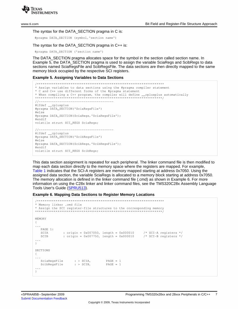
3.2 Using the DATA_SECTION Pragma to Map a Register-File Structure to Memory
The compiler produces relocatable blocks of code and data. These blocks, called sections, are allocatedin memory in a variety of ways to conform to different system configurations. The section to memory blockassignments are defined in the linker command file.
By default, the compiler assigns global and static variables like SciaRegs and ScibRegs to the .ebss or.bss section. In the case of the abstraction layer, however, the register-file variables are instead allocatedto the same memory as the peripheral's register file. Each variable is assigned to a specific data sectionoutside of .bss/ebss by using the compiler's DATA_SECTION pragma.
6 Programming TMS320x28xx and 28xxx Peripherals in C/C++ «SPRAA85B–September 2009Submit Documentation Feedback
www.ti.com Bit Field and Register-File Structure Approach
The syntax for the DATA_SECTION pragma in C is:
#pragma DATA_SECTION (symbol,"section name")
The syntax for the DATA_SECTION pragma in C++ is:
#pragma DATA_SECTION ("section name")
The DATA_SECTION pragma allocates space for the symbol in the section called section name. InExample 5, the DATA_SECTION pragma is used to assign the variable SciaRegs and ScibRegs to datasections named SciaRegsFile and ScibRegsFile. The data sections are then directly mapped to the samememory block occupied by the respective SCI registers.
Example 5. Assigning Variables to Data Sections
/********************************************************************* Assign variables to data sections using the #pragma compiler statement* C and C++ use different forms of the #pragma statement* When compiling a C++ program, the compiler will define __cplusplus automatically********************************************************************///----------------------------------------#ifdef __cplusplus#pragma DATA_SECTION("SciaRegsFile")#else#pragma DATA_SECTION(SciaRegs,"SciaRegsFile");#endifvolatile struct SCI_REGS SciaRegs;
This data section assignment is repeated for each peripheral. The linker command file is then modified tomap each data section directly to the memory space where the registers are mapped. For example,Table 1 indicates that the SCI-A registers are memory mapped starting at address 0x7050. Using theassigned data section, the variable SciaRegs is allocated to a memory block starting at address 0x7050.The memory allocation is defined in the linker command file (.cmd) as shown in Example 6. For moreinformation on using the C28x linker and linker command files, see the TMS320C28x Assembly LanguageTools User's Guide (SPRU513).
Example 6. Mapping Data Sections to Register Memory Locations
/********************************************************************* Memory linker .cmd file* Assign the SCI register-file structures to the corresponding memory********************************************************************/
Bit Field and Register-File Structure Approach www.ti.com
By mapping the register-file structure variable directly to the memory address of the peripheral's registers,you can access the registers directly in C/C++ code by simply modifying the required member of thestructure. Each member of a structure can be used just like a normal variable, but its name will be a bitlonger. For example, to write to the SCI-A Control Register (SCICCR), access the SCICCR member ofSciaRegs as shown in Example 7. Here the dot is an operator in C that selects a member from astructure.
Example 7. Accessing a Member of the SCI Register-File Structure
Accessing specific bits within the register is often useful; bit-field definitions provide this flexibility. Bit fieldsare defined within a C/C++ structure by providing a list of bit-field names. each followed by colon and thenumber of bits the field occupies.
Bit fields are a convenient way to express many difficult operations in C or C++. Bit fields do, however,suffer from a lack of portability between hardware platforms. On the C28x devices, the following rulesapply to bit fields:
• Bit field members are stored from right to left in memory. That is, the least significant bit, or bit zero, ofthe register corresponds to the first bit field.
• The C28x compiler limits the maximum number of bits within a bit field to the size of an integer; no bitfield can be greater than 16 bits in length.
• If the total number of bits defined by bit fields within a structure grows above 16 bits, then the next bitfield is stored consecutively in the next word of memory.
The SCICCR and SCICTL1 registers in Figure 1 and Figure 2 translate into the C/C++ bit-field definitionsin Example 8. Reserved locations within the register are held with bit fields that are not used except asplace holders, i.e., rsvd, rsvd1, rsvd2, et cetera. As with other structures, each member is accessed usingthe dot operator in C or C++.
www.ti.com Bit Field and Register-File Structure Approach
Example 8. SCI Control Registers Defined Using Bit Fields
/********************************************************************* SCI header file********************************************************************///----------------------------------------------------------// SCICCR communication control register bit definitions://struct SCICCR_BITS { // bit description
Uint16 SCICHAR:3; // 2:0 Character length controlUint16 ADDRIDLE_MODE:1; // 3 ADDR/IDLE Mode controlUint16 LOOPBKENA:1; // 4 Loop Back enableUint16 PARITYENA:1; // 5 Parity enableUint16 PARITY:1; // 6 Even or Odd ParityUint16 STOPBITS:1; // 7 Number of Stop BitsUint16 rsvd1:8; // 15:8 reserved
};//-------------------------------------------// SCICTL1 control register 1 bit definitions://struct SCICTL1_BITS { // bit description
While bit fields provide access to individual bits, you may still want to access the register as a singlevalue. To provide this option, a union declaration is created to allow the register to be accessed in termsof the defined bit fields or as a whole. The union definitions for the SCI communications control registerand control register 1 are shown in Example 9.
Example 9. Union Definition to Provide Access to Bit Fields and the Whole Register
Bit Field and Register-File Structure Approach www.ti.com
Once bit-field and union definitions are established for specific registers, the SCI register-file structure isrewritten in terms of the union definitions as shown in Example 10. Note that not all registers have bit fielddefinitions; some registers, such as SCITXBUF, will always be accessed as a whole and a bit fielddefinition is not necessary.
Example 10. SCI Register-File Structure Using Unions
union SCICCR_REG SCICCR; // Communications control registerunion SCICTL1_REG SCICTL1; // Control register 1Uint16 SCIHBAUD; // Baud rate (high) registerUint16 SCILBAUD; // Baud rate (low) registerunion SCICTL2_REG SCICTL2; // Control register 2union SCIRXST_REG SCIRXST; // Receive status registerUint16 SCIRXEMU; // Receive emulation buffer registerunion SCIRXBUF_REG SCIRXBUF; // Receive data bufferUint16 rsvd1; // reservedUint16 SCITXBUF; // Transmit data bufferunion SCIFFTX_REG SCIFFTX; // FIFO transmit registerunion SCIFFRX_REG SCIFFRX; // FIFO receive registerunion SCIFFCT_REG SCIFFCT; // FIFO control registerUint16 rsvd2; // reservedUint16 rsvd3; // reservedunion SCIPRI_REG SCIPRI; // FIFO Priority control
};
As with other structures, each member (.all or .bit) is accessed using the dot operator in C/C++ as shownin Example 11. When the .all member is specified, the entire register is accessed. When the .bit memberis specified, then the defined bit fields can be directly accessed.
NOTE: Writing to a bit field has the appearance of writing to only the specified field. In reality,however, the CPU performs what is called a read-modify-write operation; the entire registeris read, its contents are modified and the entire value is written back. Possible side effects ofread-modify-write instructions are discussed in Section 6.
www.ti.com Bit Field and Register-File Structure Advantages
4 Bit Field and Register-File Structure Advantages
The bit field and register-file structure approach has many advantages that include:
• Register-file structures and bit fields are already available from Texas Instruments.In the C/C++ Header Files and Peripheral Examples, the register-file structures and bit fields havebeen implemented for all peripherals on the TMS320x28xx and TMS320x28xxx devices. The includedheader files can be used as-is or extended to suit your particular needs.The complete implementation is available in the software downloads from TI's website as shown inSection 1.
• Using bit fields produces code that is easy-to-write, easy-to-read, easy-to-update, and efficient.Bit fields can be manipulated quickly without the need to determine a register mask value. In addition,you have the flexibility to access registers either by bit field or as a single quantity as shown inExample 11. Code written using the register file structures also generates very efficient code. Codeefficiency will be discussed in Section 5.
• Bit fields take advantage of the Code Composer Studio editors auto complete feature.At first it may seem that variable names are harder to remember and longer to type when usingregister-file structures and bit fields. The Code Composer Studio editor provides a list of possiblestructure/bit field elements as you type; this makes it easier to write code without referring todocumentation for register and bit field names. An example of the auto completion feature for theCPU-Timer TCR register is shown in Figure 3.
Figure 3. Code Composer Studio 3.3 Autocomplete Feature
11«SPRAA85B–September 2009 Programming TMS320x28xx and 28xxx Peripherals in C/C++Submit Documentation Feedback
Code Size and Performance Using Bit Fields www.ti.com
• Increases the effectiveness of the Code Composer Studio Watch Window.You can add and expand register-file structures in Code Composer Studio's watch window as shown inFigure 4. Bit field values are read directly without extracting their value by hand.
Figure 4. Code Composer Studio Watch Window
5 Code Size and Performance Using Bit Fields
The bit field and register-file structure approach is very efficient when accessing a single bit within aregister or when polling a bit. As an example, consider code to initialize the PCLKCR0 register on aTMS320x280x device. PCLKCR0 is described in detail in the TMS320x280x, 2801x, 2804x SystemControl and Interrupts Reference Guide (SPRU712). The bit-field definition for this register is shown inExample 12.
www.ti.com Code Size and Performance Using Bit Fields
Example 12. TMS320x280x PCLKCR0 Bit-Field Definition
// Peripheral clock control register 0 bit definitions:struct PCLKCR0_BITS { // bits description
Uint16 rsvd1:2; // 1:0 reservedUint16 TBCLKSYNC:1; // 2 eWPM Module TBCLK enable/syncUint16 ADCENCLK:1; // 3 Enable high speed clk to ADCUint16 I2CAENCLK:1; // 4 Enable SYSCLKOUT to I2C-AUint16 rsvd2:1; // 5 reservedUint16 SPICENCLK:1; // 6 Enable low speed clk to SPI-CUint16 SPIDENCLK:1; // 7 Enable low speed clk to SPI-DUint16 SPIAENCLK:1; // 8 Enable low speed clk to SPI-AUint16 SPIBENCLK:1; // 9 Enable low speed clk to SPI-BUint16 SCIAENCLK:1; // 10 Enable low speed clk to SCI-AUint16 SCIBENCLK:1; // 11 Enable low speed clk to SCI-BUint16 rsvd3:2; // 13:12 reservedUint16 ECANAENCLK:1; // 14 Enable SYSCLKOUT to eCAN-AUint16 ECANBENCLK:1; // 15 Enable SYSCLKOUT to eCAN-B
};
The code in Example 13 enables the peripheral clocks on a TMS320x2801 device. The C28x compilergenerates one assembly code instruction for each C-code register access. This is very efficient; there is aone-to-one correlation between the C instructions and the assembly instructions. The only overhead is theinitial instruction to set the data page pointer (DP).
Example 13. Assembly Code Generated by Bit Field Accesses
// Enable only 2801 Peripheral ClocksEALLOW; 3F82A7 EALLOWSysCtrlRegs.PCLKCR0.bit.rsvd1 = 0; 3F82A8 MOVW DP,#0x01C0SysCtrlRegs.PCLKCR0.bit.TBCLKSYNC = 0; 3F82AA AND @28,#0xFFFCSysCtrlRegs.PCLKCR0.bit.ADCENCLK = 1; 3F82AC AND @28,#0xFFFBSysCtrlRegs.PCLKCR0.bit.I2CAENCLK = 1; 3F82AE OR @28,#0x0008SysCtrlRegs.PCLKCR0.bit.rsvd2 = 0; 3F82B0 OR @28,#0x0010SysCtrlRegs.PCLKCR0.bit.SPICENCLK = 1; 3F82B2 AND @28,#0xFFDFSysCtrlRegs.PCLKCR0.bit.SPIDENCLK = 1; 3F82B4 OR @28,#0x0040SysCtrlRegs.PCLKCR0.bit.SPIAENCLK = 1; 3F82B6 OR @28,#0x0080SysCtrlRegs.PCLKCR0.bit.SPIBENCLK = 1; 3F82B8 OR @28,#0x0100SysCtrlRegs.PCLKCR0.bit.SCIAENCLK = 1; 3F82BA OR @28,#0x0200SysCtrlRegs.PCLKCR0.bit.SCIBENCLK = 0; 3F82BC OR @28,#0x0400SysCtrlRegs.PCLKCR0.bit.rsvd3 = 0; 3F82BE AND @28,#0xF7FFSysCtrlRegs.PCLKCR0.bit.ECANAENCLK= 1; 3F82C0 AND @28,#0xCFFFSysCtrlRegs.PCLKCR0.bit.ECANBENCLK= 0; 3F82C2 OR @28,#0x4000EDIS; 3F82C4 AND @28,#0x7FFF
3F82C6 EDIS
NOTE: EALLOW and EDIS are macros defined in the C/C++ Header Files and PeripheralExamples. These macros expand to the EALLOW and EDIS assembly instructions.
The EALLOW protection mechanism prevents spurious CPU writes to several registers.Executing EALLOW permits the CPU to write freely to protected registers and executingEDIS protects them once more. For information on EALLOW protection and a list ofprotected registers, refer to the System Control and Interrupts reference guide specific toyour device.
13«SPRAA85B–September 2009 Programming TMS320x28xx and 28xxx Peripherals in C/C++Submit Documentation Feedback
Code Size and Performance Using Bit Fields www.ti.com
To calculate how many cycles the code in Example 13 will take, you need to know how many wait statesare required to access the PCLKCR0 register. Wait state information for all memory blocks and peripheralframes is listed in the device specific data manual. The PCLKCR0 register is in peripheral frame 2; thisframe requires two wait states for a read access and no wait states for a write access. This means a readfrom PCLKCR0 takes three cycles total and a write takes one cycle. In addition, a new access toPCLKCR0 cannot begin until the previous write is complete. This built-in protection mechanism removespipeline effects and makes sure operations proceed in the correct order; all of the peripheral registershave this protection. In Example 13, each access to the PCLKCR0 register will take six cycles; thepipeline phases are shown in Table 3.
Table 3. CPU-Pipeline Activity For Read-Modify-Write Instructions in Example 13
CPU-Pipeline Phase (1)
Read 1 - Read Begins Read 2 - Data Latched Execute - Value Modified Write - Value written Cycle
1AND @28,#0xFFFC
2AND @28,#0xFFFC
3AND @28,#0xFFFC
4AND @28,#0xFFFC
5AND @28,#0xFFFC
6AND @28,#0xFFFC
7AND @28,#0xFFFB
8AND @28,#0xFFFB
9AND @28,#0xFFFB
10AND @28,#0xFFFB
11AND @28,#0xFFFB
12AND @28,#0xFFFB
13OR @28,#0x0008
14OR @28,#0x0008
15OR @28,#0x0008
16OR @28,#0x0008
17OR @28,#0x0008
18OR @28,#0x0008
OR @28,#0x0010
etc...(1) For detailed CPU pipeline information, see theTMS320C28x CPU and Instruction Set Reference Guide (SPRU430).
When code size and cycle counts must be kept to a minimum, it is beneficial to reduce the number ofinstructions required to initialize a register to as few as possible. Here are some options for reducing codesize:
• Enable the compiler's optimizer:As mentioned in Section 3.1, register-file variables are declared as volatile. For this reason, enablingthe optimizer alone will not reduce the number of instructions. The keyword volatile alerts the compilerthat the variable's value can change outside of the currently executing code. While removing thevolatile keyword would reduce code size, it is not recommended. Removing volatile must be done withgreat care and only where the developer is certain doing so will not yield incorrect results.
14 Programming TMS320x28xx and 28xxx Peripherals in C/C++ «SPRAA85B–September 2009Submit Documentation Feedback
www.ti.com Code Size and Performance Using Bit Fields
• Write to the complete register (.all union member):The union definitions discussed in Section 3.4 allow access to either specific bit fields or to the entireregister. When a write is performed to the entire register using the .all member of the union, code sizeis reduced. This method creates very efficient code as shown in Example 14. Using .all, however,makes the code both harder to write and harder to read. It is not immediately evident how different bitfields in the register are configured.
Example 14. Optimization Using the .all Union Member
• Use a shadow register and enable the compiler's optimizer:This method is the best compromise. The register's contents are loaded into a shadow register of thesame type as shown in Example 15. The content of the shadow register is then modified using bitfields. Since shadowPCLKCR0 is not volatile, the compiler will combine the bit field writes when theoptimizer is enabled. Note that all of the reserved locations are also initialized. At the end of the codethe value in the shadow register is written to PCLKCR0. This method retains the advantages of bit fielddefinitions and results in code that is easy to read. The assembly shown was generated with thecompiler's optimization level -o1 enabled.
Read-Modify-Write Considerations When Using Bit Fields www.ti.com
6 Read-Modify-Write Considerations When Using Bit Fields
When writing to a bit field, the compiler generates what is called a read-modify-write assembly instruction.Read-modify-write refers to the technique used to implement bit-wise or byte-wise operations such asAND, OR and XOR. That is, the location is read, the single bit field is modified, and the result is writtenback. Example 16 shows some of the C28x read-modify-write assembly instructions .
Example 16. A Few Read-Modify-Write Operations
AND @Var, #0xFFFC ; Read 16-bit value "Var"; AND the value with 0xFFFC; Write the 16-bit result to "Var";;
OR @Var, #0x0010 ; Read 16-bit value "Var"; OR the value with 0x0010; Write the 16-bit result to "Var";;
XOR @VarB, AL ; Read 16-bit value "Var"; XOR with AL; Write the 16-bit result to "Var";;
MOVB *+XAR2[0], AH.LSB ; Read 16-bit value pointed to by XAR2; Modify the least significant byte; Write the 16-bit value back
With a full CPU pipeline, a C28x based device can complete one read-modify-write operation to zerowait-state SARAM every cycle. When accessing the peripheral registers or external memory, however,required wait states must be taken into account. In addition, the pipeline protection mechanism can furtherstall instructions in the CPU pipeline. This is described in more detail in Section 5 and in the TMS320C28xCPU and Instruction Set Reference Guide (SPRU430).
Read-modify-write instructions usually have no ill side effects. It is important, however, to realize thatread-modify-write instructions do not limit access to only specific bits in the register; these instructionswrite to all of the register's bits. In some cases, the read-modify-write sequence can cause unexpectedresults when bits are written to with the value originally read. Registers that are sensitive toread-modify-write instructions fall into three categories:
• Registers with bits that hardware can change after the read, but before the write• Registers with write 1-to-clear bits• Registers that have bits that must be written with a value different from what the bits read back
Registers that fall into these three categories are typically found within older peripherals. To keep registercompatibility, the register files have not been redesigned to avoid this issue. Newer peripherals, such asthe ePWM, eCAP, and eQEP, however, have a register layout specifically designed to avoid theseproblems.
This section describes in detail the three categories in which read-modify-write operations should be usedwith care. In addition, an example of each type of register is given along with a suggested method forsafely modifying that register. At the end of the section a list of read-modify-write sensitive registers isprovided for reference.
6.1 Registers That Hardware Can Modify During Read-Modify-Write Operations
The device itself can change the state of some bits between the read and the write stages of the CPUpipeline. For example, the PIE interrupt flag registers (PIEIFRx where x = 1, 2, ... 12) can change due toan external hardware or peripheral event. The value written back may overwrite a flag, corrupting thevalue, and result in missed interrupts.
16 Programming TMS320x28xx and 28xxx Peripherals in C/C++ «SPRAA85B–September 2009Submit Documentation Feedback
www.ti.com Read-Modify-Write Considerations When Using Bit Fields
6.1.1 PIEIFRx Registers
If there is a need to clear a PIEIFRx bit, then the rule is to always let the CPU take the interrupt to clearthe flag. This is done by re-mapping the interrupt vector to a pseudo interrupt service routine (ISR). Thecorresponding PIEIERx bit is then set to allow the CPU to service the interrupt using the pseudo ISR.Within the pseudo ISR the interrupt vector is re-mapped to the interrupt vector for the true ISR routine asshown in Example 17.
NOTE: This rule does not apply to the CPU's IFR register. Special instructions are provided to clearCPU IFR bits and will not result in missing interrupts. Use the OR IFR instruction to set IFRbits, and use the AND IFR instruction to clear pending interrupts.
Example 17. Clearing PIEIFRx (x = 1, 2...12) Registers
// Pseudo ISR prototype. PTIN = pointer to an interruptinterrupt void PseudoISR(void);PINT TempISR;....if( PieCtrlRegs.PIEIFR1.bit.INTx4 == 1){// Temp save current vector and remap to pseudo ISR// Take the interrupt to clear the PIEIFR flagEALLOW;TempISR = PieVectTable.XINT1;PieVectTable.XINT1 = PseudoISR;PieCtrlRegs.PIEIER1.bit.INTx4 = 1;EDIS;
}....
// Pseudo ISR// Services the interrupt & the hardware clears the PIEIFR flag// Re-maps the interrupt to the proper ISRinterrupt void PseudoISR(void){EALLOW;PieVectTable.XINT1 = TempISR;EDIS;
}
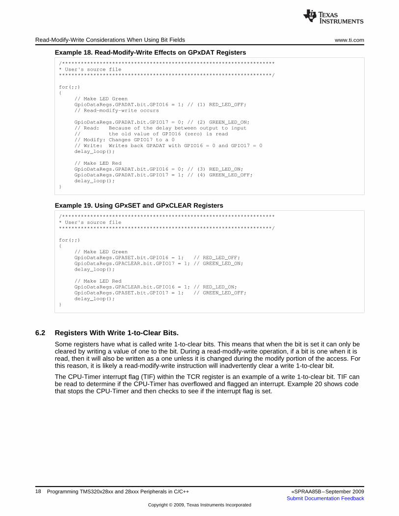
6.1.2 GPxDAT Registers
Another case of bits that can change between a read and a write are the GPIO data registers. Considerthe code shown in Example 18. Except on 281x devices, the GPxDAT registers reflect the state of the pin,not the output latch. This means the register reflects the actual pin value. However, there is a lag betweenwhen the register is written to when the new pin value is reflected back in the register. This may pose aproblem when this register is used in subsequent program statements to alter the state of GPIO pins. InExample 18 two program statements attempt to drive two different GPIO pins. The second instruction willwait for the first to finish its write due to the write-followed-by-read protection on this peripheral frame.There will be some lag, however, between the write of GPIO16 and the GPxDAT bit reflecting the newvalue (1) on the pin. During this lag, the second instruction will read the old value of GPIO16 (0) and writeit back along with the new value of GPIO17 (0). Therefore, the GPIO16 pin stays low.
One solution is to put some NOP’s between the read-modify-write instructions. A better solution is to usethe GPxSET/GPxCLEAR/GPxTOGGLE registers instead of the GPxDAT registers. These registers alwaysread back a 0 and writes of 0 have no effect. Only bits that need to be changed can be specified withoutdisturbing any other bit(s) that are currently in the process of changing. The same code using GPxSETand GPxCLEAR registers is shown in Example 19.
17«SPRAA85B–September 2009 Programming TMS320x28xx and 28xxx Peripherals in C/C++Submit Documentation Feedback
// Make LED GreenGpioDataRegs.GPADAT.bit.GPIO16 = 1; // (1) RED_LED_OFF;// Read-modify-write occurs
GpioDataRegs.GPADAT.bit.GPIO17 = 0; // (2) GREEN_LED_ON;// Read: Because of the delay between output to input// the old value of GPIO16 (zero) is read// Modify: Changes GPIO17 to a 0// Write: Writes back GPADAT with GPIO16 = 0 and GPIO17 = 0delay_loop();
// Make LED RedGpioDataRegs.GPADAT.bit.GPIO16 = 0; // (3) RED_LED_ON;GpioDataRegs.GPADAT.bit.GPIO17 = 1; // (4) GREEN_LED_OFF;delay_loop();
// Make LED GreenGpioDataRegs.GPASET.bit.GPIO16 = 1; // RED_LED_OFF;GpioDataRegs.GPACLEAR.bit.GPIO17 = 1; // GREEN_LED_ON;delay_loop();
// Make LED RedGpioDataRegs.GPACLEAR.bit.GPIO16 = 1; // RED_LED_ON;GpioDataRegs.GPASET.bit.GPIO17 = 1; // GREEN_LED_OFF;delay_loop();
}
6.2 Registers With Write 1-to-Clear Bits.
Some registers have what is called write 1-to-clear bits. This means that when the bit is set it can only becleared by writing a value of one to the bit. During a read-modify-write operation, if a bit is one when it isread, then it will also be written as a one unless it is changed during the modify portion of the access. Forthis reason, it is likely a read-modify-write instruction will inadvertently clear a write 1-to-clear bit.
The CPU-Timer interrupt flag (TIF) within the TCR register is an example of a write 1-to-clear bit. TIF canbe read to determine if the CPU-Timer has overflowed and flagged an interrupt. Example 20 shows codethat stops the CPU-Timer and then checks to see if the interrupt flag is set.
18 Programming TMS320x28xx and 28xxx Peripherals in C/C++ «SPRAA85B–September 2009Submit Documentation Feedback
// Stop the CPU-TimerCpuTimer0Regs.TCR.bit.TSS = 1; 3F80C7 MOVW DP,#0x0030
3F80C9 OR @4,#0x0010// Check to see if TIF is set 3F80CB TBIT @4,#15if (CpuTimer0Regs.TCR.bit.TIF == 1) 3F80CC SBF L1,NTC{ 3F80CD NOP
// TIF set, insert action here 3F80CE L1:// NOP is only a place holder ....asm(" NOP");
}
The test for TIF in Example 20 will never be true even if an interrupt has been flagged. The OR assemblyinstruction to set the TSS bit performs a read-modify-write operation on the TCR register. If the TIF bit isset when the read-modify-write operation occurs, then TIF will be read as a 1 and also written back as a 1.The TIF bit will always be cleared as a result of this write. To avoid this, the write to TIF bit always be 0.The TIF bit ignores writes of 0, thus, its value will be preserved. One possible implementation thatpreserves TIF is shown in Example 21.
Example 21. Using a Shadow Register to Preserve Write 1-to-Clear Bits
union TCR_REG shadowTCR;// Use a shadow register to stop the timer// and preserve TIF (write 1-to-clear bit)shadowTCR.all = CpuTimer0Regs.TCR.all; 3F80C7 MOVW DP,#0x0030shadowTCR.bit.TSS = 1; 3F80C9 MOV AL,@4shadowTCR.bit.TIF = 0; 3F80CA ORB AL,#0x10CpuTimer0Regs.TCR.all = shadowTCR.all; 3F80CB MOVL XAR5,#0x000C00
3F80CD AND AL,@AL,#0x7FFF// Check the TIF flag 3F80CF MOV *+XAR5[4],ALif(CpuTimer0Regs.TCR.bit.TIF == 1) 3F80D0 TBIT *+XAR5[4],#15{ 3F80D1 SBF L1,NTC
// TIF set, insert action here 3F80D2 NOP// NOP is only a place holder 3F80D3 L1:asm(" NOP");
}
The content of the TCR register is copied into a shadow register. Within the shadow register the TSS bit isset, and the TIF bit is cleared. The shadow register is then written back to TCR; the timer is stopped andthe state of TIF is preserved. The assembly instructions were generated with optimization level -o2enabled.
6.3 Register Bits Requiring a Specific Value
Some registers have bits that must be written as a specific value. If this value is different from the valuethe bits read, then a read-modify-write operation will likely write the incorrect value.
An example is the watchdog check bit field (WDCHK) in the watchdog control register. The watchdogcheck bits must be written as 1,0,1; any other value is considered illegal and will reset the device. Sincethese bits always read back as 0,0,0, a read-modify-write operation will write 0,0,0 unless WDCHK ischanged during the modify portion of the operation.
19«SPRAA85B–September 2009 Programming TMS320x28xx and 28xxx Peripherals in C/C++Submit Documentation Feedback
Read-Modify-Write Considerations When Using Bit Fields www.ti.com
Another solution is to avoid the read-modify-write operation and instead only write a 16-bit value to theWDCR register. To remind you of this requirement, a bit field definition is not provided for the WDCRregister in the C/C++ Header Files and Peripheral Examples. Registers that do not have bit-field nor uniondefinitions are accessed without the .bit or .all designations as shown in Example 22.
See the TMS320x280x, 2801x, 2804x DSP System Control and Interrupts Reference Guide (SPRU712)and TMS320x281x System Control and Interrupts Reference Guide (SPRU078) for more information onthe watchdog module.
6.4 Read-Modify-Write Sensitive Registers
Table 4 lists registers that are sensitive to read-modify-write instructions. Depending on the register andhow the peripheral is used in the application, effects of a read-modify-write operation may or may not be aconcern. This list may not be complete.
Table 4. Read-Modify-Write Sensitive Registers
Module Register(s) Comments
Watchdog SCSR WDOVERRIDE is a write 1-to-clear bit and alwaysreads back as a 1.
WDCR WDCHK must be written as 1,0,1 and always readback as 0,0,0.
WDCR WDFLG is a write 1-to-clear bit.
CPU-Timer TCR Timer interrupt flag (TIF) is a write 1-to-clear bit.
GPIO GPxDAT Use this register to read data and instead use theSET/CLEAR and TOGGLE registers to change thestate of GPIO pins.
PIE PIEIFRx To clear PIEIFR bits, do not write to the PIEIFRregister. Instead map the interrupt to a "pseudo"interrupt and service it. That is, let the hardware clearthe interrupt flag otherwise interrupts from otherperipherals may be missed.
PIEACKx The PIEACK bits are write 1-to-clear bits.
Event Manager (EV) (1) CAPCONA CAPCONB CAPRES is a write-0-to-reset bit and always readsback as 0.
CAPFIFOA CAPFIFOB If a write occurs at the same time that a CAPxFIFOstatus bit is being updated, the write data takesprecedence. Thus if the bit changes between theread and the write phase of a read-modify-writeinstruction, the new bit value may be lost.
EVAIFRA/B/C EVBIFRA/B/C The EV interrupt flags are all write 1-to-clear bits.
eCAN CANTRS CANTRR The eCAN module can change the state of a bitbetween the time the register is read and the time itis written back.
CANTA CANAA These registers contain one or more write 1-to-clearCANRMP CANRML bits.CANRFP CANESCANGIF0 CANGIF1CANTOS
SPI SPIST Contains write 1-to-clear bits.
I2C I2CSTR Contains write 1-to-clear bits.
(1) The EV module is available on TMS320x281x devices only.
20 Programming TMS320x28xx and 28xxx Peripherals in C/C++ «SPRAA85B–September 2009Submit Documentation Feedback
Access to peripherals occur on one of three peripheral frames (or busses). Peripheral registers arelocated in the frame capable of accesses that best fit the register set.
• Peripheral frame 0:Peripherals within this frame are on the device's memory bus. This bus is capable of both 16-bit or32-bit accesses. For example, CPU-Timers are on the memory bus.
• Peripheral frame 1:Peripheral frame 1 uses a bus that is capable of both 16-bit and 32-bit accesses. Examples include theePWM and eCAN peripherals.
• Peripheral frame 2:Peripheral frame 2 uses a bus that is capable of only 16-bit accesses. All of the peripheral registers onframe 2 are only 16-bits in length. Examples include the SCI, SPI, ADC and I2C.
The eCAN control and status registers are limited to 32-bit-wide accesses. Accesses of only 16 bits canyield unpredictable results. The eCAN control and status registers must be handled as a special case;they are the only peripheral frame 1 registers limited to 32-bit wide accesses.
Often the compiler will reduce an access to 16-bits if it will save code size or improve performance. Caremust be taken to make sure what appears to be a 32-bit access to the eCAN control and status registersis not simplified to a 16-bit access by the compiler. For example, the compiler has reduced the accessshown in Example 23 to a 16-bit access to half of the CANMC register.
Example 23. Invalid eCAN Control Register 16-Bit Write
// The compiler will simplify this to 3F81FA EALLOW// a 16-bit read-modify-write 3F81FB MOVW DP,#0x0180EALLOW; 3F81FD OR @20,#0x2000ECanaRegs.CANMC.bit.SCB = 1; 3F81FF EDISEDIS;
To force 32-bit accesses, the bit-field definitions and read-modify-write operations must not be used. Theregister must be read and written using the .all member of the union definition and all 32-bits must be reador written.
Unfortunately, not using bit fields or read-modify-write operations reduces the code readability. Onesolution is to read the entire register into a shadow register, manipulate the value, and then write the new32-bit value to the register using .all. The code in Example 24 uses a shadow register to force a 32-bitaccess. If more then one register is going to be accessed, then the whole eCAN register file can beshadowed (i.e., struct ECAN_REGS shadowECanaRegs;).
Example 24. Using a Shadow Register to Force a 32-Bit Access
IMPORTANT NOTICETexas Instruments Incorporated and its subsidiaries (TI) reserve the right to make corrections, modifications, enhancements, improvements,and other changes to its products and services at any time and to discontinue any product or service without notice. Customers shouldobtain the latest relevant information before placing orders and should verify that such information is current and complete. All products aresold subject to TI’s terms and conditions of sale supplied at the time of order acknowledgment.TI warrants performance of its hardware products to the specifications applicable at the time of sale in accordance with TI’s standardwarranty. Testing and other quality control techniques are used to the extent TI deems necessary to support this warranty. Except wheremandated by government requirements, testing of all parameters of each product is not necessarily performed.TI assumes no liability for applications assistance or customer product design. Customers are responsible for their products andapplications using TI components. To minimize the risks associated with customer products and applications, customers should provideadequate design and operating safeguards.TI does not warrant or represent that any license, either express or implied, is granted under any TI patent right, copyright, mask work right,or other TI intellectual property right relating to any combination, machine, or process in which TI products or services are used. Informationpublished by TI regarding third-party products or services does not constitute a license from TI to use such products or services or awarranty or endorsement thereof. Use of such information may require a license from a third party under the patents or other intellectualproperty of the third party, or a license from TI under the patents or other intellectual property of TI.Reproduction of TI information in TI data books or data sheets is permissible only if reproduction is without alteration and is accompaniedby all associated warranties, conditions, limitations, and notices. Reproduction of this information with alteration is an unfair and deceptivebusiness practice. TI is not responsible or liable for such altered documentation. Information of third parties may be subject to additionalrestrictions.Resale of TI products or services with statements different from or beyond the parameters stated by TI for that product or service voids allexpress and any implied warranties for the associated TI product or service and is an unfair and deceptive business practice. TI is notresponsible or liable for any such statements.TI products are not authorized for use in safety-critical applications (such as life support) where a failure of the TI product would reasonablybe expected to cause severe personal injury or death, unless officers of the parties have executed an agreement specifically governingsuch use. Buyers represent that they have all necessary expertise in the safety and regulatory ramifications of their applications, andacknowledge and agree that they are solely responsible for all legal, regulatory and safety-related requirements concerning their productsand any use of TI products in such safety-critical applications, notwithstanding any applications-related information or support that may beprovided by TI. Further, Buyers must fully indemnify TI and its representatives against any damages arising out of the use of TI products insuch safety-critical applications.TI products are neither designed nor intended for use in military/aerospace applications or environments unless the TI products arespecifically designated by TI as military-grade or "enhanced plastic." Only products designated by TI as military-grade meet militaryspecifications. Buyers acknowledge and agree that any such use of TI products which TI has not designated as military-grade is solely atthe Buyer's risk, and that they are solely responsible for compliance with all legal and regulatory requirements in connection with such use.TI products are neither designed nor intended for use in automotive applications or environments unless the specific TI products aredesignated by TI as compliant with ISO/TS 16949 requirements. Buyers acknowledge and agree that, if they use any non-designatedproducts in automotive applications, TI will not be responsible for any failure to meet such requirements.Following are URLs where you can obtain information on other Texas Instruments products and application solutions:Products ApplicationsAmplifiers amplifier.ti.com Audio www.ti.com/audioData Converters dataconverter.ti.com Automotive www.ti.com/automotiveDLP® Products www.dlp.com Broadband www.ti.com/broadbandDSP dsp.ti.com Digital Control www.ti.com/digitalcontrolClocks and Timers www.ti.com/clocks Medical www.ti.com/medicalInterface interface.ti.com Military www.ti.com/militaryLogic logic.ti.com Optical Networking www.ti.com/opticalnetworkPower Mgmt power.ti.com Security www.ti.com/securityMicrocontrollers microcontroller.ti.com Telephony www.ti.com/telephonyRFID www.ti-rfid.com Video & Imaging www.ti.com/videoRF/IF and ZigBee® Solutions www.ti.com/lprf Wireless www.ti.com/wireless


![TMS320x28xx Digital Signal Processors-[DM]-[SPRS174]](https://static.documents.pub/doc/80x56/54a12fc6ac7959c87d8b4690/tms320x28xx-digital-signal-processors-dm-sprs174.jpg)


