1 Progress in Magnetoresistive Memory: Magnetic Tunnel Junctions with a Composite Free Layer Alexander Makarov, Viktor Sverdlov, and Siegfried Selberherr Institute for Microelectronics, TU Wien, Vienna, A-1040, Austria [email protected]Received 24 March 2014 Accepted 20 June 2014 Magnetoresistive memory is a candidate for future universal memory because of fast switching, high density, and non-volatility. However, improvement regarding the essential parameters such as thermal stability and switching current is still needed and finding alternative architectures for magnetic cell structures is of considerable importance for the success of magnetoresistive memory. A structure with a composite free layer displays significant switching time reduction without sacrificing the thermal stability. In this work we discuss the progress in development of structures with a composite free layer from first suggestions to structurally optimized cells. We compare the most important parameters of a newly proposed optimized structure with a composite free layer, which are the switching time, the thermal stability, and the switching energy barrier, with a conventional structure with a monolithic free layer. Keywords: STT-MRAM; micromagnetic simulation; composite free layer. 1. Introduction Today’s magnetic memory technology is represented by magnetoresistive RAM (MRAM) and spin transfer torque MRAM (STT-MRAM) 1 . The basic element of a MRAM and STT-MRAM cell is a sandwich of two magnetic layers separated by a non- magnetic conducting spacer layer or a thin insulating layer. While the magnetization of the reference layer (RL) is fixed due to the fabrication process, the magnetization direction of the free layer (FL) can be switched between the two states parallel and anti- Fig. 1. Schematic illustration of a magnetic pillar in a high resistance (left) and low resistance (right) state.
Transcript
1
Progress in Magnetoresistive Memory: Magnetic Tunnel Junctions with a Composite Free Layer
Alexander Makarov, Viktor Sverdlov, and Siegfried Selberherr
Institute for Microelectronics, TU Wien, Vienna, A-1040, Austria
Magnetoresistive memory is a candidate for future universal memory because of fast switching, high density, and non-volatility. However, improvement regarding the essential parameters such as thermal stability and switching current is still needed and finding alternative architectures for magnetic cell structures is of considerable importance for the success of magnetoresistive memory. A structure with a composite free layer displays significant switching time reduction without sacrificing the thermal stability. In this work we discuss the progress in development of structures with a composite free layer from first suggestions to structurally optimized cells. We compare the most important parameters of a newly proposed optimized structure with a composite free layer, which are the switching time, the thermal stability, and the switching energy barrier, with a conventional structure with a monolithic free layer.
Today’s magnetic memory technology is represented by magnetoresistive RAM (MRAM) and spin transfer torque MRAM (STT-MRAM)1. The basic element of a MRAM and STT-MRAM cell is a sandwich of two magnetic layers separated by a non-magnetic conducting spacer layer or a thin insulating layer. While the magnetization of the reference layer (RL) is fixed due to the fabrication process, the magnetization direction of the free layer (FL) can be switched between the two states parallel and anti-
Fig. 1. Schematic illustration of a magnetic pillar in a high resistance (left) and low resistance (right) state.
2 A. Makarov, V. Sverdlov & S. Selberherr
parallel to the fixed magnetization direction. Anti-parallel and parallel states possess different magnetoresistances which are mapped to 0 and 1 (Fig. 1).
In conventional field-driven MRAM the free layer magnetization switching is performed by applying a magnetic field1. In contrast to field-driven MRAM, STT-MRAM does not require an external magnetic field. Switching between the two states occurs due to spin transfer torque produced by the spin-polarized current flowing through the pillar.
STT-MRAM based on a magnetic tunnel junction (MTJ) is a promising candidate for future universal memory because of small area demand, unlimited endurance, non-volatility, and long retention2, 3, 4. There are two competing classes of MTJs with different directions of magnetization of the free layer: in-plane and perpendicular. Each of the classes has advantages and disadvantages. Perpendicular MTJs (p-MTJs) with an interface-induced anisotropy show potential, but still require a reduction of damping and an increase of thermal stability. The in-plane MTJs exhibit a high thermal stability, but still require a reduction of the critical current density. However, improvement regarding the essential parameters including reduction of the switching current density is still needed. Finding alternative architectures for MTJ structures is of considerable importance for the success of STT-MRAM.
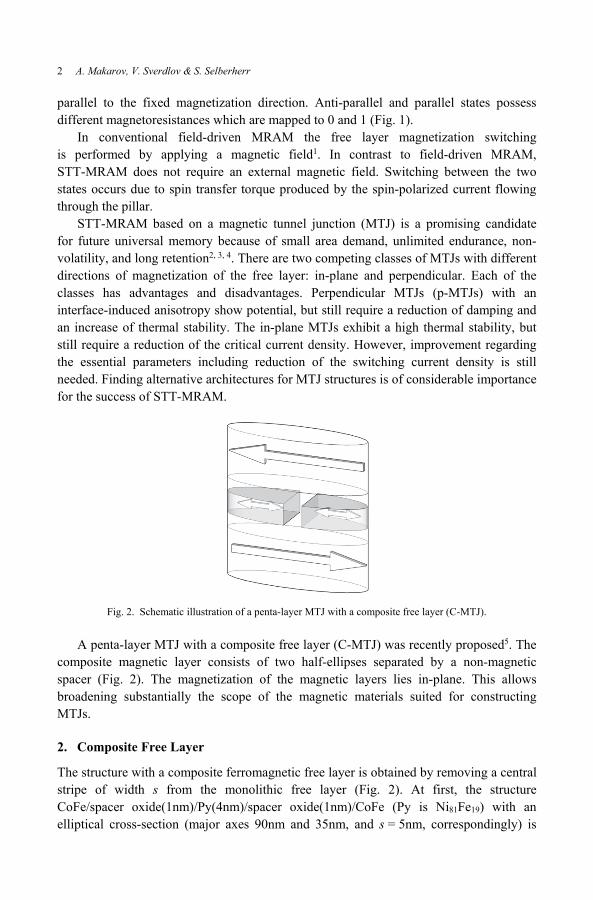
Fig. 2. Schematic illustration of a penta-layer MTJ with a composite free layer (C-MTJ).
A penta-layer MTJ with a composite free layer (C-MTJ) was recently proposed5. The composite magnetic layer consists of two half-ellipses separated by a non-magnetic spacer (Fig. 2). The magnetization of the magnetic layers lies in-plane. This allows broadening substantially the scope of the magnetic materials suited for constructing MTJs.
2. Composite Free Layer
The structure with a composite ferromagnetic free layer is obtained by removing a central stripe of width s from the monolithic free layer (Fig. 2). At first, the structure CoFe/spacer oxide(1nm)/Py(4nm)/spacer oxide(1nm)/CoFe (Py is Ni81Fe19) with an elliptical cross-section (major axes 90nm and 35nm, and s = 5nm, correspondingly) is
Progress in Magnetoresistive Memory 3
investigated. In order to simplify the identification of the important features related to switching for such structures, they are assumed to be symmetric (the spacer layers are equivalent). It should be noted that for an asymmetric structure it is possible to achieve a symmetric switching time.
Our simulations of penta-layer structure switching are based on the magnetization dynamics described by the Landau-Lifschitz-Gilbert (LLG) equation with additional spin torque terms6:
2
1
2
1
( )
B
s
ddt
g j ge M d
g
eff eff
1 1
2 2
m m H m m H
m p m m p
m p m m p
(1)
Here, γ = 2.3245·105m/(A·s) is the gyromagnetic ratio, α is the Gilbert damping parameter, μB is the Bohr magneton, j is the current density, e is the electron charge, d is the thickness of the free layer, m = M/Ms is the position dependent normalized vector of the magnetization in the free layer, p1 = Mp1/Msp1 and p2 = Mp2/Msp2 are the normalized magnetizations in the first and second pinned layers, respectively. Ms, Msp1, and Msp2 are the saturation magnetizations of the free layer, the first pinned layer, and the second pinned layer, correspondingly.
Slonczewski’s expression g(θ) depends on the spacer layer material, and for a non-magnetic conducting spacer layer it is expressed by7:
13 3/2( ) 4 (1 ) (3 cos( )) / 4
g . (2)
Here, η is the polarizing factor7. For thin insulating spacer layer Slonczewski’s expression is given by8:
12( ) 0.5 1 cos( )
g . (3)
The local effective field is calculated as:
eff ext ani exch demag th amp msH H H H H H H H . (4)
Hext is the external field, Hani is the magnetic anisotropy field, Hexch is the exchange field, Hdemag is the demagnetizing field, Hth is the thermal field, Hamp is the Ampere field, and Hms is the magnetostatic coupling field between the pinned and the free layers.
Contrary to the standard consideration, we do not assume the reference layers being fully compensated. They produce the magnetostatic field Hms, which couples the pinned layers and the free layer, thus offering an additional degree of freedom to improve the characteristics of the system.
This non-compensated field causes the magnetization of the free layer to tilt out of the x-y plane. The non-zero angle between the fixed magnetization and the magnetization in the free layer results in an enhanced spin transfer torque, when the current starts flowing
4 A. Makarov, V. Sverdlov & S. Selberherr
perpendicular to the x-y plane. In the case of the monolithic structure, however, the torque remains marginal in the central region, where the magnetization is along the x-axis. As the amplitude of the end domains’ precession increases, the central region experiences almost no spin torque and preserves its initial orientation along the x-axis, thus preventing the whole layer from alternating its magnetization orientation. This is, however, not the case when the central region is removed in the composite structure and the end domains become virtually independent. Fig. 3a demonstrates a substantial decrease of the switching time in the penta-layer structure with the composite free layer, for the same current density, as a function of the thickness of the pinned ferromagnetic layers. The switching process for the pinned layer thicknesses of 5nm, 15nm, and 20nm is shown in Fig. 3b. Due to the removal of the central region, which represented the “bottleneck” for switching in the monolithic structure, the shape anisotropy energy decreases (Fig. 3b, inset). However, its value is still sufficiently large for guaranteeing the thermal stability at operation conditions9.
The switching time in a penta-layer structure with a composite free layer is decreasing, if the thickness of the pinned layers is increased. This is due to the fact that the z-component of the magnetostatic field Hms (Fig. 3a, bottom inset) increases together with the pinned layer thickness, causing a larger initial angle (Fig. 3a, top inset) between the relaxed magnetization in the domains of the free layer and the magnetization of the pinned layer, a larger torque, and, as a consequence, a shorter switching time.
Fig. 3. (a) Ratio of the switching time in the monolithic structure vs. the switching time in the composite structure as function of the thickness of the pinned layer. The insets show the averaged initial angle (top) and the dependence of the absolute values of the z-component of the averaged magnetostatic field (bottom). (b) Switching process for MTJs with a composite free layer for pinned layer thicknesses of 5nm, 15nm, and 20nm (from right to left). The inset shows the shape anisotropy energy as function of the thickness of the pinned layer for a monolithic (circles) and a composite (squares) free layer.
In this section only a first description and a raw explanation of the fast switching phenomenon in the structure with the composite free layer were given. In the following the phenomenon is discussed in detail.
Progress in Magnetoresistive Memory 5
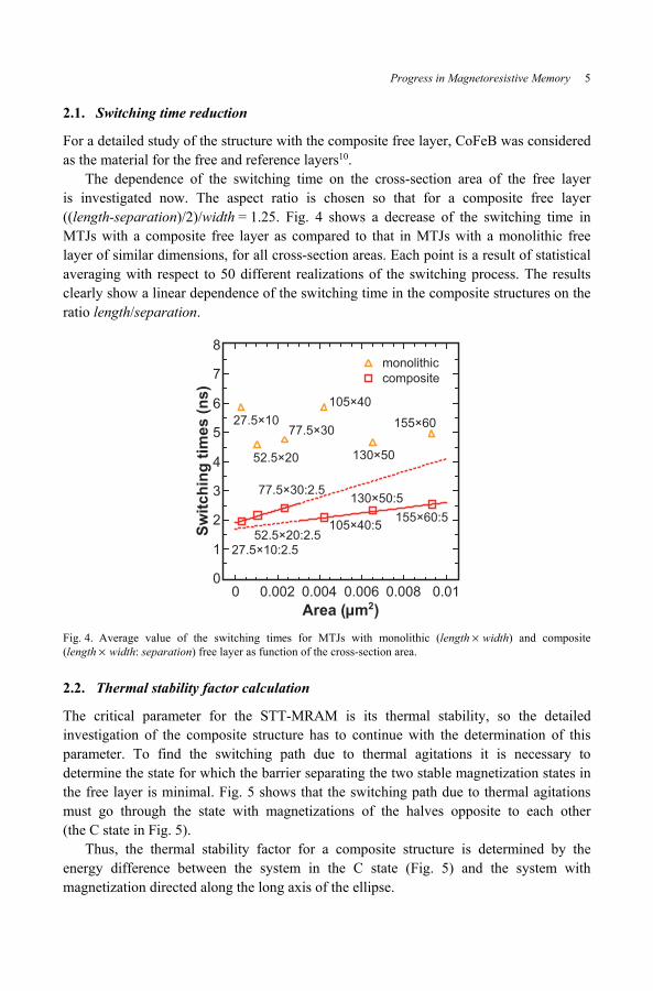
2.1. Switching time reduction
For a detailed study of the structure with the composite free layer, CoFeB was considered as the material for the free and reference layers10.
The dependence of the switching time on the cross-section area of the free layer is investigated now. The aspect ratio is chosen so that for a composite free layer ((length-separation)/2)/width = 1.25. Fig. 4 shows a decrease of the switching time in MTJs with a composite free layer as compared to that in MTJs with a monolithic free layer of similar dimensions, for all cross-section areas. Each point is a result of statistical averaging with respect to 50 different realizations of the switching process. The results clearly show a linear dependence of the switching time in the composite structures on the ratio length/separation.
Fig. 4. Average value of the switching times for MTJs with monolithic (length width) and composite (length width: separation) free layer as function of the cross-section area.
2.2. Thermal stability factor calculation
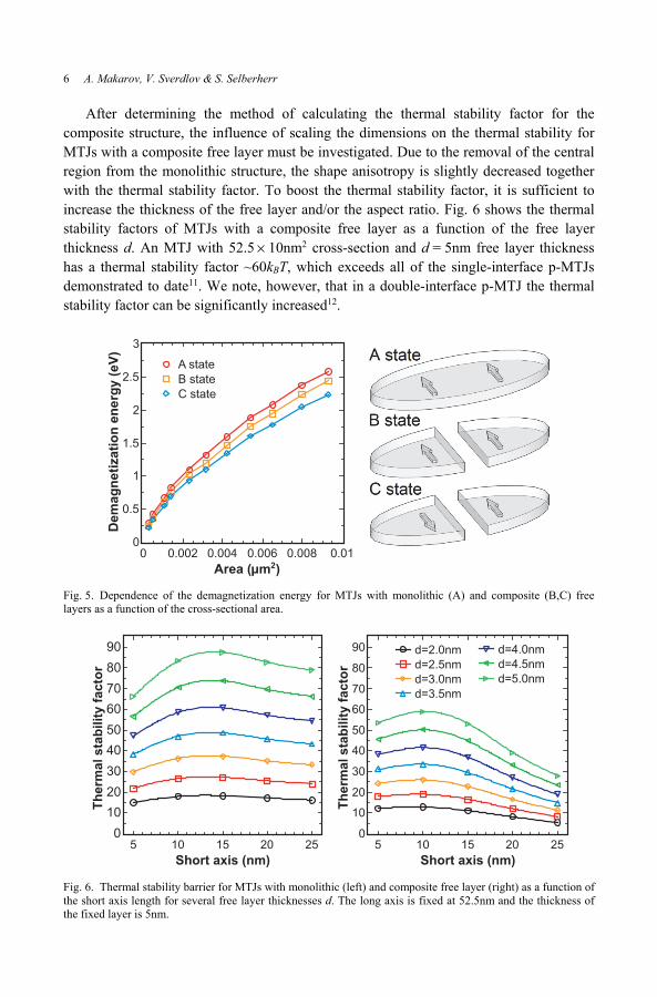
The critical parameter for the STT-MRAM is its thermal stability, so the detailed investigation of the composite structure has to continue with the determination of this parameter. To find the switching path due to thermal agitations it is necessary to determine the state for which the barrier separating the two stable magnetization states in the free layer is minimal. Fig. 5 shows that the switching path due to thermal agitations must go through the state with magnetizations of the halves opposite to each other (the C state in Fig. 5).
Thus, the thermal stability factor for a composite structure is determined by the energy difference between the system in the C state (Fig. 5) and the system with magnetization directed along the long axis of the ellipse.
6 A. Makarov, V. Sverdlov & S. Selberherr
After determining the method of calculating the thermal stability factor for the composite structure, the influence of scaling the dimensions on the thermal stability for MTJs with a composite free layer must be investigated. Due to the removal of the central region from the monolithic structure, the shape anisotropy is slightly decreased together with the thermal stability factor. To boost the thermal stability factor, it is sufficient to increase the thickness of the free layer and/or the aspect ratio. Fig. 6 shows the thermal stability factors of MTJs with a composite free layer as a function of the free layer thickness d. An MTJ with 52.5 10nm2 cross-section and d = 5nm free layer thickness has a thermal stability factor ~60kBT, which exceeds all of the single-interface p-MTJs demonstrated to date11. We note, however, that in a double-interface p-MTJ the thermal stability factor can be significantly increased12.
Fig. 5. Dependence of the demagnetization energy for MTJs with monolithic (A) and composite (B,C) free layers as a function of the cross-sectional area.
Fig. 6. Thermal stability barrier for MTJs with monolithic (left) and composite free layer (right) as a function of the short axis length for several free layer thicknesses d. The long axis is fixed at 52.5nm and the thickness of the fixed layer is 5nm.
Progress in Magnetoresistive Memory 7
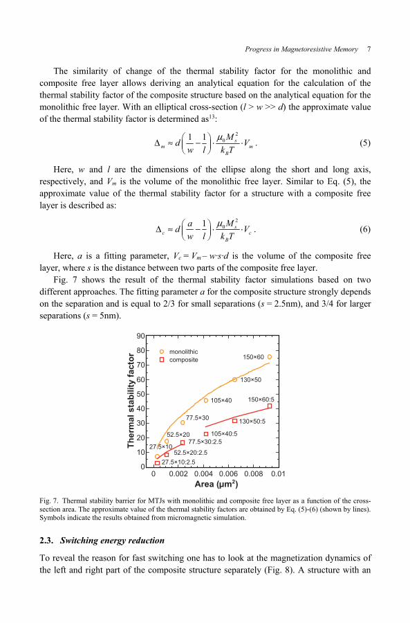
The similarity of change of the thermal stability factor for the monolithic and composite free layer allows deriving an analytical equation for the calculation of the thermal stability factor of the composite structure based on the analytical equation for the monolithic free layer. With an elliptical cross-section (l > w >> d) the approximate value of the thermal stability factor is determined as13:
201 1
sm m
B
Md Vw l k T
. (5)
Here, w and l are the dimensions of the ellipse along the short and long axis, respectively, and Vm is the volume of the monolithic free layer. Similar to Eq. (5), the approximate value of the thermal stability factor for a structure with a composite free layer is described as:
201
sc c
B
Mad Vw l k T
. (6)
Here, a is a fitting parameter, Vc = Vm – w·s·d is the volume of the composite free layer, where s is the distance between two parts of the composite free layer.
Fig. 7 shows the result of the thermal stability factor simulations based on two different approaches. The fitting parameter a for the composite structure strongly depends on the separation and is equal to 2/3 for small separations (s = 2.5nm), and 3/4 for larger separations (s = 5nm).
Fig. 7. Thermal stability barrier for MTJs with monolithic and composite free layer as a function of the cross-section area. The approximate value of the thermal stability factors are obtained by Eq. (5)-(6) (shown by lines). Symbols indicate the results obtained from micromagnetic simulation.
2.3. Switching energy reduction
To reveal the reason for fast switching one has to look at the magnetization dynamics of the left and right part of the composite structure separately (Fig. 8). A structure with an
8 A. Makarov, V. Sverdlov & S. Selberherr
elliptical 52.5 25nm2 cross-section and the following layer sequence is considered: CoFeB(5nm)/ MgO(1nm)/ CoFeB(2nm)/ MgO(1nm)/ CoFeB(5nm). The central 2.5nm stripe is removed from the middle CoFeB layer. Fig. 8b and Fig. 8c show that the switching processes of the left and right parts of the composite free layer occur in opposite senses to each other. Most importantly, the magnetizations of each piece stay practically in-plane. Because the magnetization does not go out-of-plane, as during the switching of the monolithic free layer, this switching behavior should lead to a decrease of the switching energy barrier. It turns out that the switching paths by current and due to thermal fluctuations are similar. Thus, as in p-MTJs, the switching barrier in the composite structure becomes practically equal to the thermal stability barrier defined by the shape anisotropy of the composite free layer structure. The reduction of the switching barrier leads to the reduction of the switching time in the composite structure as compared to the conventional MTJ at the same switching current density.
In the following the height of the thermal energy barrier is compared with that of the switching energy barrier (Fig. 9). As expected from the analysis of the magnetization dynamics, the switching barrier becomes practically equal to the thermal stability barrier.
Fig. 8. Magnetization components vs. time for an elliptical 52.5 25nm2 MTJ with a composite free layer. The magnetization of the left and right halves is shown separately.
Fig. 9. Thermal energy (lines) vs. switching energy (symbols) for the composite structure. The long axis is fixed at 52.5nm and the thickness of the fixed layer is 5nm. Dependences are shown for short axes of 5nm, 10nm, 15nm, 20nm, and 25nm length. Each point is a result of statistical averaging with respect to 30 different realizations of the switching process.
Progress in Magnetoresistive Memory 9
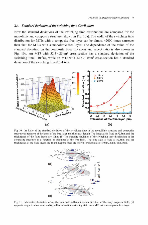
2.4. Standard deviation of the switching time distribution
Now the standard deviations of the switching time distributions are compared for the monolithic and composite structure (shown in Fig. 10a). The width of the switching time distribution for MTJs with a composite free layer can be almost ~2000 times narrower than that for MTJs with a monolithic free layer. The dependence of the value of the standard deviation on the composite layer thickness and aspect ratio is also shown in Fig. 10b. An MTJ with 52.5 25nm2 cross-section has a standard deviation of the switching time ~10–3ns, while an MTJ with 52.5 10nm2 cross-section has a standard deviation of the switching time 0.3-1.6ns.
(a) (b)
Fig. 10. (a) Ratio of the standard deviation of the switching time in the monolithic structure and composite structure as function of thickness of the free layer and short axis length. The long axis is fixed at 52.5nm and the thicknesses of the fixed layers are 10nm. (b) The standard deviation of the switching time distribution in the composite structure as a function of thickness of the free layer. The long axis is fixed at 52.5nm and the thicknesses of the fixed layers are 15nm. Dependences are shown for short axis of 10nm, 20nm, and 25nm.
Fig. 11. Schematic illustration of (a) the state with self-stabilization direction of the stray magnetic field, (b) opposite magnetization state, and (c) self-acceleration switching state in an MTJ with a composite free layer.
10 A. Makarov, V. Sverdlov & S. Selberherr
In order to find a physical explanation for the distribution narrowing, the switching process is analyzed in detail14. A schematic illustration of the self-stabilization and self-acceleration principle of switching in a composite free layer is explained in Fig. 11. Each half of the free layer generates a stray magnetic field which influences the other half and helps stabilizing the switching process. This stray magnetic field increases with growing short axis which leads to the switching times’ distribution narrowing. Before the moment when the magnetizations of the different halves of the composite layer are in opposite directions to each other (Fig. 11b), the stray magnetic field acts as a stabilizing factor for switching (Fig. 11a). After the opposite magnetization state is reached the stray magnetic fields accelerate switching as illustrated in Fig. 11c.
3. Structure Optimization of the Composite Free Layer
In this section a structural optimization of the composite free layer is presented by means of extensive micromagnetic simulations and a new structure for the composite free layer is proposed15. To distinguish the two types of composite free layers, the notation for an MTJ with the free layer consisting of two equivalent parts of half-elliptic form separated by a narrow non-magnetic spacer is introduced as C-MTJ (Fig. 2) and C2-MTJ for the new structure.
Fig. 12. Schematic illustration of: (a) C2-MTJ and (b) M2-MTJ.
The free layer of the C2-MTJ (Fig. 12a) is composed of two ellipses with the axes a/2 and b inscribed into a rectangle a b. Thus, the newly proposed structure does not require a narrow gap between the two parts of the composite layer, and therefore can be easily fabricated. Next, the most important parameters of STT-MRAM devices, switching time, thermal stability, and switching energy barrier of C2-MTJ, C-MTJ, conventional MTJ with monolithic free layer, and an M2-MTJ structure with one small free layer of elliptical shape (Fig. 12b) are compared.
3.1. Switching time and standard deviation
First, the time of switching of C2-MTJs is discussed and compared with those of C-MTJs. Fig. 13 shows the dependence of the switching time on the thicknesses of the
Progress in Magnetoresistive Memory 11
free layer for three values of the short axis: 10nm, 15nm, and 20nm. The long axis is fixed at 52.5nm. The simulations demonstrate that C2-MTJs and C-MTJs have practically equal switching times for all considered cross-sections of the free layer.
Fig. 13. Switching time of C-MTJs (symbols) and C2-MTJs (lines) as function of the thickness of the free layer. The long axis is fixed at 52.5nm and the thickness of the fixed layer is 5nm. Dependences are shown for short axes of 10nm, 15nm, and 20nm length. Each point is a result of statistical averaging with respect to 30 different realizations of the switching process.
Fig. 14. Ratio of the switching times in the monolithic structure and composite structure as function of thickness of the free layer and short axis length. The long axis is fixed at 52.5nm. Dependences are shown for: (a) conventional MTJ vs. C2-MTJ, (b) M2-MTJ vs. C2-MTJ.
The fact that the switching times in C-MTJs and C2-MTJs are equal also means a switching acceleration for C2-MTJs as compared to the conventional MTJ with a monolithic free layer. This is indeed confirmed by the results of the simulations shown in Fig. 14a. Fig. 14b demonstrates that C2-MTJs exhibit almost the same switching times as the structure with a single small ellipse (M2-MTJ, Fig. 12b).
12 A. Makarov, V. Sverdlov & S. Selberherr
Fig. 15. The standard deviation of the switching time distribution in the C2-MTJ structure as function of the thickness of the free layer. The long axis is fixed at 52.5nm and the thickness of the fixed layer is 15nm. Dependences are shown for the short axis of 10nm, 20nm, and 25nm. Each point is a result of statistical averaging with respect to 30 different realizations of the switching process.
Now the standard deviations of the switching time distributions in C-MTJs and C2-MTJs are compared. The dependence of the standard deviation on composite layer thickness and aspect ratio for the C2-MTJ is shown in Fig. 15. With 52.5 25nm2 cross-section a standard deviation of the switching time ~10–3ns is obtained for both structures, while with 52.5 10nm2 cross-section the standard deviation of the switching time is 0.3-1.6ns for the C-MTJ (Fig. 10b) and 0.09-0.9ns for the C2-MTJ (Fig. 15). Thus C2-MTJs show a ~2-3 times narrower distribution of the switching times as compared to the C-MTJs at a large aspect ratio of the free layer.
3.2. Thermal stability factor
Now the thermal stability factor for the two types of the composite layer structures, C-MTJ and C2-MTJ, are compared. Fig. 16a confirms that the replacement of the free layer consisting of the two half-ellipses separated with a narrow gap (C-MTJ) by only two small ellipses (C2-MTJ) does not result in a loss of thermal stability. With 52.5 10nm2 cross-section and 5nm thickness of the free layer a thermal stability factor ~60kBT is obtained.
Next, the thermal stability factor for the C2-MTJ is compared with that of the two structures with monolithic free layer, conventional MTJ and M2-MTJ. Due to the removal of the central region from the monolithic structure the shape anisotropy in the C2-MTJ is decreased together with the thermal stability factor (Fig. 16b). The constant ratio of the thermal stability factor as a function of the aspect ratio and thicknesses of the free layer indicates that the thermal stability factors for both structures scales similarly. This means that in order to increase the thermal stability factor in C2-MTJs it is sufficient to increase the thickness of the free layer and/or the aspect ratio.
Progress in Magnetoresistive Memory 13
Fig. 16. (a) Thermal stability factor for C-MTJs (symbols) and C2-MTJs (lines) as function of the thickness of the free layer. Each point is a result of statistical averaging with respect to 30 different realizations of the switching process. (b) Ratio of the thermal stability factors for monolithic structure and composite structure as function of thickness of the free layer and short axis length. Dependences are shown for the ratios: M2-MTJ to C2-MTJ (solid lines), conventional MTJ to C2-MTJ (dotted lines). The long axis is fixed at 52.5nm and the thickness of the fixed layer is 5nm. Dependences are shown for short axes of 10nm, 15nm, and 20nm length.
In comparison to the second structure with the monolithic free layer, M2-MTJ, the C2-MTJ shows a gain in thermal stability by a factor of ~2 times (Fig. 16b), while maintaining the same switching time (Fig. 14b), confirming the superiority of the C2-MTJ over the M2-MTJ.
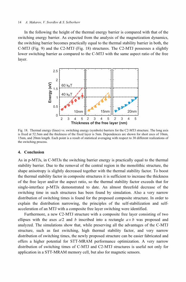
3.3. Switching energy
To determine the reason of the fast switching in C2-MTJs the switching process was investigated in detail. Fig. 17 shows that, as in a C-MTJ, the switching processes of the left and right part of the C2-MTJ’s free layer occur in opposite senses to each other. Importantly, the switching occurs in the x-y plane. This is clearly seen at the time instance for 1.9ns, when the left and right ellipses pass simultaneously through the state (0;-1;0) and (0;1;0) respectively (Fig. 17).
Fig. 17. Magnetization components vs. time for an elliptical 52.5 20nm2 C2-MTJ. The magnetization of the left and right halves is shown separately.
14 A. Makarov, V. Sverdlov & S. Selberherr
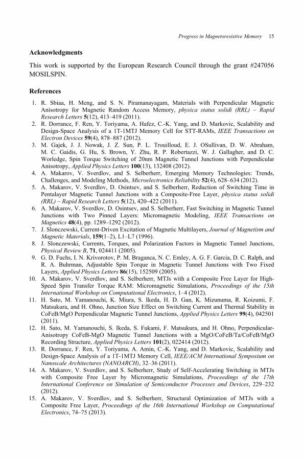
In the following the height of the thermal energy barrier is compared with that of the switching energy barrier. As expected from the analysis of the magnetization dynamics, the switching barrier becomes practically equal to the thermal stability barrier in both, the C-MTJ (Fig. 9) and the C2-MTJ (Fig. 18) structures. The C2-MTJ possesses a slightly lower switching barrier as compared to the C-MTJ with the same aspect ratio of the free layer.
Fig. 18. Thermal energy (lines) vs. switching energy (symbols) barriers for the C2-MTJ structure. The long axis is fixed at 52.5nm and the thickness of the fixed layer is 5nm. Dependences are shown for short axes of 10nm, 15nm, and 20nm length. Each point is a result of statistical averaging with respect to 30 different realizations of the switching process.
4. Conclusion
As in p-MTJs, in C-MTJs the switching barrier energy is practically equal to the thermal stability barrier. Due to the removal of the central region in the monolithic structure, the shape anisotropy is slightly decreased together with the thermal stability factor. To boost the thermal stability factor in composite structures it is sufficient to increase the thickness of the free layer and/or the aspect ratio, so the thermal stability factor exceeds that for single-interface p-MTJs demonstrated to date. An almost threefold decrease of the switching time in such structures has been found by simulation. Also a very narrow distribution of switching times is found for the proposed composite structure. In order to explain the distribution narrowing, the principles of the self-stabilization and self-acceleration of an MTJ with a composite free layer switching were identified.
Furthermore, a new C2-MTJ structure with a composite free layer consisting of two ellipses with the axes a/2 and b inscribed into a rectangle a b was proposed and analyzed. The simulations show that, while preserving all the advantages of the C-MTJ structure, such as fast switching, high thermal stability factor, and very narrow distribution of switching times, the newly proposed structure can be easier fabricated and offers a higher potential for STT-MRAM performance optimization. A very narrow distribution of switching times of C-MTJ and C2-MTJ structures is useful not only for application in a STT-MRAM memory cell, but also for magnetic sensors.
Progress in Magnetoresistive Memory 15
Acknowledgments
This work is supported by the European Research Council through the grant #247056 MOSILSPIN.
References
1. R. Sbiaa, H. Meng, and S. N. Piramanayagam, Materials with Perpendicular MagneticAnisotropy for Magnetic Random Access Memory, physica status solidi (RRL) – RapidResearch Letters 5(12), 413–419 (2011).
2. R. Dorrance, F. Ren, Y. Toriyama, A. Hafez, C.-K. Yang, and D. Markovic, Scalability andDesign-Space Analysis of a 1T-1MTJ Memory Cell for STT-RAMs, IEEE Transactions onElectron Devices 59(4), 878–887 (2012).
3. M. Gajek, J. J. Nowak, J. Z. Sun, P. L. Trouilloud, E. J. OSullivan, D. W. Abraham,M. C. Gaidis, G. Hu, S. Brown, Y. Zhu, R. P. Robertazzi, W. J. Gallagher, and D. C.Worledge, Spin Torque Switching of 20nm Magnetic Tunnel Junctions with PerpendicularAnisotropy, Applied Physics Letters 100(13), 132408 (2012).
4. A. Makarov, V. Sverdlov, and S. Selberherr, Emerging Memory Technologies: Trends,Challenges, and Modeling Methods, Microelectronics Reliability 52(4), 628–634 (2012).
5. A. Makarov, V. Sverdlov, D. Osintsev, and S. Selberherr, Reduction of Switching Time inPentalayer Magnetic Tunnel Junctions with a Composite-Free Layer, physica status solidi(RRL) – Rapid Research Letters 5(12), 420–422 (2011).
6. A. Makarov, V. Sverdlov, D. Osintsev, and S. Selberherr, Fast Switching in Magnetic TunnelJunctions with Two Pinned Layers: Micromagnetic Modeling, IEEE Transactions onMagnetics 48(4), pp. 1289–1292 (2012).
7. J. Slonczewski, Current-Driven Excitation of Magnetic Multilayers, Journal of Magnetism andMagnetic Materials, 159(1–2), L1–L7 (1996).
8. J. Slonczewski, Currents, Torques, and Polarization Factors in Magnetic Tunnel Junctions,Physical Review B, 71, 024411 (2005).
9. G. D. Fuchs, I. N. Krivorotov, P. M. Braganca, N. C. Emley, A. G. F. Garcia, D. C. Ralph, andR. A. Buhrman, Adjustable Spin Torque in Magnetic Tunnel Junctions with Two FixedLayers, Applied Physics Letters 86(15), 152509 (2005).
10. A. Makarov, V. Sverdlov, and S. Selberherr, MTJs with a Composite Free Layer for High-Speed Spin Transfer Torque RAM: Micromagnetic Simulations, Proceedings of the 15thInternational Workshop on Computational Electronics, 1–4 (2012).
11. H. Sato, M. Yamanouchi, K. Miura, S. Ikeda, H. D. Gan, K. Mizunuma, R. Koizumi, F.Matsukura, and H. Ohno, Junction Size Effect on Switching Current and Thermal Stability inCoFeB/MgO Perpendicular Magnetic Tunnel Junctions, Applied Physics Letters 99(4), 042501(2011).
12. H. Sato, M. Yamanouchi, S. Ikeda, S. Fukami, F. Matsukura, and H. Ohno, Perpendicular-Anisotropy CoFeB-MgO Magnetic Tunnel Junctions with a MgO/CoFeB/Ta/CoFeB/MgORecording Structure, Applied Physics Letters 101(2), 022414 (2012).
13. R. Dorrance, F. Ren, Y. Toriyama, A. Amin, C.-K. Yang, and D. Markovic, Scalability andDesign-Space Analysis of a 1T-1MTJ Memory Cell, IEEE/ACM International Symposium onNanoscale Architectures (NANOARCH), 32–36 (2011).
14. A. Makarov, V. Sverdlov, and S. Selberherr, Study of Self-Accelerating Switching in MTJswith Composite Free Layer by Micromagnetic Simulations, Proceedings of the 17thInternational Conference on Simulation of Semiconductor Processes and Devices, 229–232(2012).
15. A. Makarov, V. Sverdlov, and S. Selberherr, Structural Optimization of MTJs with aComposite Free Layer, Proceedings of the 16th International Workshop on ComputationalElectronics, 74–75 (2013).