PROJECT FINAL REPORT (PUBLIC) Grant Agreement number: 258407 Project acronym: GALACTICO Project title: blendinG diverse photonics And eLectronics on silicon for integrAted and fully funCTIonal COherent Tb Ethernet Funding Scheme: CP/STREP Period covered: from 1/10/2010 to 30/09/2013 Name, title and organisation of the scientific representative of the project's coordinator: Dr Lars Zimmermann Tel: +49 (335) 5625-407 Fax: +49 (335) 5625-327 E-mail: [email protected]Name, title and organisation of the scientific representative of the project's technical manager: Dr Leontios Stampoulidis Tel: +30 211 800 5152 Fax: +30 211 800 5565 E-mail: [email protected]Project website Fehler! Textmarke nicht definiert. address: http://www.ict-galactico.eu
Transcript
PROJECT FINAL REPORT (PUBLIC)
Grant Agreement number: 258407
Project acronym: GALACTICO
Project title: blendinG diverse photonics And eLectronics on silicon for integrAted and fully funCTIonal COherent Tb Ethernet
board and flip-chip InP PDs (precursor towards full silicon integration with nano-waveguides
and Ge diodes)
Component & module testing objectives
Perform lab trials and benchmark against commercially available modulators with QPSK and
16/32 QAM modulation formats at 28-32 Gbaud
Perform field trial and evaluate performance under co-existence with commercial DWDM
OTN platforms with QPSK modulation formats at 28-32 Gbaud
1.3 Main S&T results/foregrounds GALACTICO SiPh coherent receivers
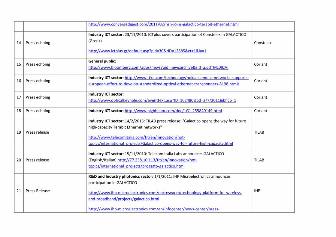
On the receiver side work was focused on breaking the PIC size limits with the fabrication of
coherent receiver SiPh PICs on nano-waveguides and the employment of high speed Ge diodes and
electronics using a BiCMOS process. GALACTICO implemented this route progressively;
“First gen” GALACTICO: the first gen GALACTICO DP coherent receiver modules relied on the
cost-effective hybrid integration of high performance pre-fabricated InP potodetectors on
medium index contrast 4 um SiPh boards.
“Next gen” GALACTICO: the final gen GALACTICO DP coherent receiver modules relied on
the unique combination of Ge diodes and SiPh nano-waveguide boards leveraging the
strengths of BiCMOS fabrication.
More specifically GALACTICO demonstrated:
1. Fabrication of SP and DP hybrid integrated InP on Si coherent receiver module.
2. Fabrication of Ge diodes demonstrating cut-off frequencies well above 30 GHz and internal
responsivity of approximately 0.7 A/W
3. Design of a complete family of SiPh nano-waveguide components for miniaturized coherent
receivers including 2D gratings for optical coupling and polarization splitting and optical hybrid
for phase decoding
4. Fabrication & characterization of record small nano-waveguide Si/Ge dual polarization coherent
receiver PIC. The PIC demonstrates a 100-fold reduction in size with respect to low/medium
index contrast waveguide technologies squeezing optical, coupling, polarization splitting and
photodetection in a record small PIC area of 5.3 mm x 2.2 mm.
One of the most interesting aspects of the Ge diode integration was that the baseline fabrication
process was designed to fit into the BiCMOS full flow to allow for a later BiCMOS integration, which
would be the next step to address manufacturability, cost and volume production with the most
efficient way. In the final project phase - and although not originally planned - GALACTICO realized
this next step by demonstrating a full flow BiCMOS integration with the fabrication of a BiCMOS
integrated Ge-PD with transimpedance amplifier. The component testing provided a very promising
result at 20 Gb/s; through GALACTICO “photonic BiCMOS” are on their way and are fully capable to
be further exploited for future component generations.
As already mentioned, the key advantage of GALACTICO coherent receiver technology is the
reduction of the coherent receiver chips incorporating the PBS, the optical 90° hybrids as well as
the Ge photodetector array down to a record size of just 2 mm x 1 mm making the coherent
receiver compatible with the upcoming CFP, CFP2 and CFP4 form factors. Compared to its
counterparts in InP technology, where the PBS is not integrated on the one hand and which is
bigger in size on the other hand, this technology is considered an enabling technology for next
generation ultra-compact SIP modules. The size advantage of the coherent receiver in
nanowaveguide technology is however enabling even more compact sub-systems compared to
present sub-systems if we take the perspective of electronic-photonic co-integration on a single
chip, as demonstrated during GALACTICO. The GALACTICO dual-polarization coherent receiver
photonic integrated circuit may be merged with high-speed transimpedance amplifier circuits in
BiCMOS technology. This has been illustrated in the following figure by merging layouts of the
respective circuits, indicating the strong potential for footprint reduction in case of electronic-
photonic integration solutions based on silicon nanowaveguide technology. Such small sub-systems
are enabled by SiPh electronic-photonic integrated circuits.
Evolution of GALACTICO coherent receiver fabrication. The figure illustrates the progressive migration from hybrid integrated InP/Si to Ge/4 um SOI and finally to Ge/nano-SOI DP coherent receiver PICs to achieve a 100x chip size reduction accommodated by a significant advantage in manufacturability; coherent receiver PICs can be cost-effectively fabricated in CMOS foundries using standard micro-electronics toolset.
GALACTICO modulators
GALACTICO modulator development route started with the optimization of the basic building block
(IQ modulator) to address the bandwidth and size targets and progressively moved towards
functionality and line rate increase. The “final gen” GALACTICO modulator prototypes performed
the dual polarization functionality on the module level and were demonstrated to generate DP-
QPSK and DP-16 QAM modulation formats at symbol rates as high as 32 Gbaud.
GALACTICO implemented this route through the following steps:
1. the fabrication of an optimized GaAs IQ modulator and modulator array reaching a 3-dB
bandwidth of >27 GHz and 20 dB ER addressing the symbol rate requirement of 28-32
Gbaud
2. the testing of the GaAs IQ modulator array with QPSK, 16 QAM, 32 QAM and 64 QAM at 25
Gbaud demonstrating successfully the scaling of the single polarization line rate from 50 up
to 150 Gb/s
3. the module assembly of the final optimized high-speed GaAs IQ modulator and its successful
system testing with up to 32 Gbaud DP-QPSK (128 Gb/s) in both lab and field trials (DP
emulation)
4. the demonstration of a monolithic GaAs DP-IQ modulator and its successful testing with DP-
QPSK at 25 Gbaud (100 Gb/s)
5. the demonstration of optimized DP functionality with the assembly of a GALACTICO twin
GaAs IQ modulator with free space polarization optics (FSPO) and its testing with DP-QPSK
and DP-16 QAM at up to 32 Gbaud, demonstrating 256 Gb/s line rate
6. the direct benchmarking of the IQ and DP-IQ GaAs modulators against commercially
available 100G DP modules and the interoperability testing with commercial 100G OTN
platforms
The graph below illustrates the fabrication course and the advancements in terms of demonstrated
bit rates in the various lab and system trials. The course involved fabrication of diverse component
generations (optimized IQ, monolithic DP, FSPO-DP) and 4 different system test rounds executed in
ICCS labs, Coriant labs, TILAB lab and installed link and Karlsruhe Institute of technology (KIT) labs
(part of a cross FP7-ICT project collaboration).
Evolution of GALACTICO modulator development. The figure illustrates the progressive development from high speed IQ GaAs to DP-IQ GaAs modulators and their demonstrations in a series of system trials with QPSK, 16 QAM, 32 QAM and 64 QAM at 25-32 Gbaud symbol rates. The demonstrated single polarization bit rate is stretched up to 150 Gb/s and the demonstrated DP bit rate has reached 256 Gb/s meeting the targets of upcoming “mini super-channel” 400G and beyond systems
Regarding transmitter devices modulator results have been complemented by adequate electronic
Performance of GALACTICO multi-level driver IC in IHP high-performance SiGe BiCMOS. Exemplifying, single-ended multilevel eye-diagram at 30 Gbaud. In a DP-QPSK scheme, this would enable an implementation with 240Gbps.
GALACTICO module testing GALACTICO modules have been tested in a series of lab and field trials demonstrating performance
at various symbol rates spanning from 22 up to 32 Gbaud and with a broad series of modulation
formats spanning from the current 100G DP-QPSK standard to upcoming DP-16 QAM and DP-32
QAM and up to “more futuristic” DP-64 QAM.
GALACTICO testing activity involved:
1. demonstration of up to 25 Gbaud SP-QPSK, SP-16 QAM, SP-32 QAM, SP-64 QAM in lab trials
2. demonstration of 28-32 Gbaud DP-QPSK and 10 Gbaud DP-16 QAM in lab trial
3. demonstration of 28-32 Gbaud DP-QPSK and DP-16 QAM in lab trial
4. demonstration of 28-32 Gbaud DP-QPSK WDM field trial
Highlight results are illustrated in the figure above. Lab trials were executed in ICCS labs, Coriant
labs, TILAB lab and Karlsruhe Institute of Technology (KIT) labs as part of a cross FP7-ICT project
collaboration. Here we summarize the activity of the field trial done using an installed fibre link in
Telecom Italia Regional Network. The trial involved transmission of 32 Gbaud QPSK signals
generated by GALACTICO modulators and the transmission with commercial 100G WDM OTN
platforms.
The field trial had the goal of testing the provided optical platform in a real DWDM system
configuration, focusing on interoperability of existing and commercially available 40 Gb/s and 100
Gb/s channels with the channels provided by the project. This has been done by inserting them in a
DWDM system employing G.652 fibres installed in the regional Telecom Italia network.
Geographical map with network exchange sites (Torino, Settimo, Volpiano, Chivasso)
Eight fibre pairs in Telecom Italia domestic metro regional network were devoted to GALACTICO
experiments. Each pair starts in TILAB “Optical Transmission Lab” and ends around 40 km far, in
Chivasso Fehler! Verweisquelle konnte nicht gefunden werden.Figure above). Each fibre belongs
to the metro regional Telecom Italia network and has a unique fibre and cable identifier code; some
network exchanges are placed in between; intra-exchange optical interconnections were made with
optical patch-cords into network exchange distribution optical patch panels.
Optical interconnections have been made in various network exchanges for the trial period. The overall link is composed by five sections of different length. In order to obtain a fibre span starting and terminating in TILAB, a hardware physical loop was done in Chivasso site: in the end, eight 80 km spans were available for the trial, each of them starting and terminating in TILAB. Some experimental activities were performed on the installed fibre plant. Preliminary cable OTDR measurements have been made; afterwards optical line amplifiers were inserted after each 80 km span in order to concatenate them and realize a long haul transmission link. The figure below shows the spectrum allocation of the wavelength channels that were used for the
field-trial experiment at TILAB premises, in order to validate and compare the performance of the
GALACTICO IQ modulator, operating together with commercial 40 and 100 Gb/s line-cards. A total
number of five equidistant data channels in a 50 GHz WDM grid were launched with an optical
power of 2 dBm per channel and OSNR of ~45dB in the field-installed fibre, with channel 3 (the
middle one) occupied by the GALACTICO transmitter at a wavelength of 1554.422 nm. Its adjacent
channels (channels 2 and 4) were selected to be commercial 112 Gb/s DP-QPSK line cards as well,
whereas channels 1 and 5 were chosen to be 43Gb/s DP -PSK linecards. At the entry point of the
network, all channels were filtered by a 50 GHz wavelength selective switch (WSS), amplified and
power-equalized in order to have the same power level, and coupled for fibre transmission in the
link.
Spectrum allocation of the WDM field trial in a 50 GHz grid GALACTICO transmitter achieved error-free transmission below the FEC limit (1·10-3) with a BER of
3.45∙10-4, over seven 80 km fibre-spans, that correspond to a total transmission length of 560 km
SMF fibre. It should be noted that even though the GALACTICO transmitter was operated with half
the required voltage swing, its performance was similar to its adjacent 112 Gb/s DP-QPSK channels.
More specifically, channels 2 and 4 were also evaluated at the end of the transmission seven span
linkand achieved a BER of 2.4∙10-4 and 5.6∙10-4 respectively.
The BER evaluation of these channels was performed individually, through their embedded
monitoring software of their linecards. GALACTICO transmitter successfully achieved 560 km
transmission in realistic network conditions with a BER of 4.45∙10-3, which is well below the soft-
decision FEC limit of 2·10-2.
The GALACTICO transmitter operating symbol rate was stretched to 32 Gbaud. Under these
conditions GALACTICO transmitter successfully achieved 560 km transmission in realistic network
conditions with a BER of 4.45∙10-3, which is well below the soft-decision FEC limit of 2·10-2.
The figures below illustrate typical results with 28 and 32 Gbaud QPSK format at the link output.
Constellation diagrams and BER of 28 Gbaud DP-QPSK at the link output, with the GALACTICO IQ modulator.
Constellation diagrams and BER of 32 Gbaud DP-QPSK at the link output, with the GALACTICO IQ modulator.
1.4 Potential impact The major potential for impact of the GALACTICO project is lower cost and miniaturization of components and modules by future scientific and economical exploitation of the developments undertaken in the areas of silicon photonics nanowaveguide receiver technology and GaAs-modulator technology. Technology The existing DP-QPSK modulator devices are targeted at line speeds of 100Gbits/s; the next generation is proffered at 400Gbits/s. The dual DP-QPSK module developed as part of the GALACTICO project offers an excellent foundation to addresses the 400Gbits/s next generation line speed. It is unlikely that a single DP-QPSK device will achieve long-haul line speeds of 400Gbits. A more likely scenario is via the use of n-QAM modulation format such that a single DP-QPSK device will achieve 200Gbits/s. (This project has demonstrated the possibility of a single DP-QPSK device achieving speeds of 300Gbit/s – 150Gbits/s per QPSK (IQ) modulator arm). Thus to achieve a line speed of 400Gbits/s two DP-QPSK devices would be required.
This module evolution is now considered very relevant for the next steps towards 400G. At the time GALACTICO was starting the debate for the next standard (400G or 1T) was still open. However under strong guidance by the system vendor and continuous monitoring of the standardization efforts, the project focus was shifted towards 400G mini-super-channels – an approach that is now becoming the technology of choice for OIF.
At present, the technology of choice for coherent receivers is based on InP as it is almost mature. However, due to the extremely high pressure on the market because of prices, cost reduction actions are highly needed. The coherent receiver modules developed in the frame of the GALACTICO project have already shown that silicon photonic technology has the potential to highly reduce the costs. This is not only due to the fact that silicon technology has strong ability to reduce cost per die, but also because, compared to its InP counterpart where e.g. additional PBS optics are needed, fully functional chips (including PBS, 90° hybrids and PDs) at much smaller sizes can be realized. As a consequence of both, lower cost and miniaturization, silicon photonics technology can perfectly match the requirements for next generation devices and also opens an access to the emerging CFP module market. In summary it can be stated that the lessons learnt via the GALACTICO project enable an efficient way for keeping or increasing the strong market position for coherent receivers as, due to the high cost pressure at the market, it is indispensable to reduce the complete manufacturing costs of the modules in order to keep the gross margin high. Furthermore, due to the extremely small footprint of the fully functional chips it offers a way for easy integrating inside CFP modules needed for the upcoming pluggable transceiver market. Manufacturing IHP and TUB have established the JointLab initiative - a research collaboration relationship for technology transfer from academia to industry. In order to sustain and further develop the technology transfer process, the two organizations are seeking for activities that will trigger photonics R&D focusing on the industrialization of silicon photonics technology with fabrication done using a qualified BiCMOS toolset.
Within the third year of GALACTICO, the technology transfer from TUB to IHP has been concluded through the design and fabrication of nano-waveguide coherent receiver chipsets. The nano-waveguides are fabricated using the IHP foundry BiCMOS toolset and the receiver chips re-present a 100-fold chip real estate reduction with respect to low/medium contrast photonic integration platforms (e.g. silica on silicon) that require specialized fabrication facilities. The IHP – TUB collaboration was effective in realizing the project’s strategic decision (taken during Y2) to switch from the SOI micro-meter scale rib waveguide technology to the nano-meter scale waveguide SOI platform in order to overcome chip size and manufacturability issues. Part of the photonic circuit design and chip characterization was done at TUB and the chip fabrication was done at IHP. The incorporation of Ge diodes fabricated at IHP on the nano-waveguide coherent receivers, has opened the way for monolithic silicon coherent receiver chips that combine high performance with low production cost. The value chain was completed ideally with the assembly of the chipsets into standardized coherent receiver modules by U2t-DE, a European leader in the development and commercialization of receiver modules. Going beyond the lifetime of the project, the target is to investigate the further steps required so that the process/foundry service becomes qualified for commercial production as well as to address the production qualification of the new receiver components. GALACTICO has been pivotal at the first steps of IHP toward industrialization of Silicon photonics technology. Today, there are several international entities promising Silicon photonic commercialization to potential customers. Most efforts focus on pure SiPh PIC (photonic integrated circuit) technology, i.e. without drive and receive electronics. The reasons for that is speed limitation of CMOS technology, which requires very advanced CMOS nodes (both bulk and SOI) to achieve the transisitor frequency required for future line rates. Since the commercial case for full SiPh integration in CMOS technologies is not clear, there is a push for advanced packaging technologies to integrate SiPh with electronics (copper nail technology or microbumps and through Si-via (TSV) technology). These approaches are less compatible with SME-type prototype and development strategies due to involved costs and the problems associated with IP safety. Here IHP developments discriminate from all other providers. IHP targets front-end integrated photonic BiCMOS. The advantages of photonic BiCMOS are in tight integration and high-speed bipolar transistors, offering next generation performance capabilities at reduced NRE (non-recurring engineering) costs. The Germanium photodetector development undertaken within the project has been a key element for the first generation of fully integrated receivers in photonic BiCMOS. Several preliminary requirements for industrialization of IHP photonic BiCMOS technology have been addressed in course of the project due to the development targets defined by the consortium partners.
2. Use and dissemination of foreground This section describes the dissemination measures, including any scientific publications relating to foreground generated during project execution.
Information and public-domain results were facilitated through the following dissemination mechanisms:
Project website
Issuing of press releases
Interviews with analysts
Organization of events
Publishing of technical publications (invited and contributed)
Project posters and flyers
dissemination through electronic or printed media (mainstream technology websites and magazines)
Depending on the nature of the audience in each action, different aspects and information was conveyed for reaching the scientific community, the industry
and the general public.
Scientific Publications
Year - Conference Paper title
2014
1 SPIE Ph West 2014
Stefanos Dris, Christos Spatharakis, Paraskevas Bakopoulos, Ioannis Lazarou, Hercules Avramopoulos,
“Blind SNR estimation for QAM constellations based on the signal magnitude statistics,” accepted for
presentation at SPIE Photonics West, San Francisco, USA, Feb. 1-6, 2014.
2 SPIE Ph West 2014
Ioannis Lazarou, Christos Spatharakis, Vasilis Katopodis, Stefanos Dris, Paraskevas Bakopoulos, Bernhard Schrenk,
- Optical Internetworking Forum – OIF - International Telecommunication Union – ITU‐T - Institute of Electrical and Electronics Engineers ‐ IEEE 802.3 - Metro Ethernet Forum – (MEF) - European Telecommunication Standards Institute – ETSI - Internet Engineering Task Force – IETF - Telecommunications Industry Association ‐ TIA
Coriant
Chair in OIF physical layer working group (PLUG)
2 Optical Internetworking Forum – OIF U2t
Other dissemination activities
Type Type of Audience - Activity description Beneficiary involved
1 Presentation
Students higher education: Presentation to members of the Electrical Engineering
Students European Association EESTEC Constelex
2 Presentation General Public: Invited presentation to Entrepreneurship& Carrier Forum 2012 session
trend in micro/nano technology. Constelex
3 Presentation Industry Aerospace sector - European Space Agency (ESA): GALACTICO presentation to
ESA telecom managers (ESA premises) Constelex
4 Presentation Students - high school: Presentation to students of the Greek YES Program - Youth
Entrepreneurship Summer Program Constelex
5 Presentation Students - University: dissemination to undergraduate and post-graduate students ICCS/NTUA, TU
Berlin
6 Interview General public: GALACTICO technical manager interview in BBC. “Greek geeks seek hi-
tech recovery”. Constelex
7 Interview
General public: GALACTICO technical manager interview in ARD German radio station,
“Made in Germany” program of Deutsche Welle TV and «ΗΜΕΡΗΣΙΑ» high circulation
Greek newspaper.
Constelex
8 Interview
Industry ICT sector, Industry photonic components: "u2t Photonics pushes balanced