Project: “Hot Carrier solar cell: Implementation of the Ultimate PV Converter” Final Report April 2012 This project is a composite project involving four nodes • PIs: Gavin Conibeer and Martin Green, University of New South Wales (UNSW) • PI: Jean-François Guillemoles, Institut de Recherche et Développement sur l'Energie Photovoltaïque, Paris (IRDEP) • PI: Tim Schmidt, University of Sydney (USyd) • PIs: Antonio Marti and Antonio Luque, Instituto de Energia Solar-UPM, Madrid (IES-UPM) Abstract Hot carrier solar cells offer the possibility of very high efficiencies (limiting efficiency 68% for un-concentrated illumination) but with a structure that could be conceptually simple compared to other very high efficiency PV devices. The challenges to produce such devices fall into 2 categories: (i) keeping carriers hot without heating the lattice and (ii) achieving a fast extraction of hot carriers through a narrow allowed energy range. (i) Methods to slow the rate of carrier cooling in an absorber material by enhancing the phonon bottleneck effect are investigated. This restricts the loss of energy to phonons, or heat in the lattice, by allowing a non-equilibrium phonon population to scatter some of its energy back to electrons. (ii) Double barrier resonant tunneling structures using quantum dots or quantum wells are investigated to give a narrow range of high conductance to select specific energies. A great strength of this project is that it synergistically combines the significant experience in all three generations of photovoltaics at the University of New South Wales (UNSW), with that on intermediate band cells and QD characterisation at Instituto de Energia Solar (IES-UPM), with the pioneering work on Hot Carrier cells at IRDEP, Paris, in conjunction with UNSW and with the excellent optical expertise and facilities at Sydney University (USyd). Modelling of the efficiencies of hot carrier cells with real material parameters have been carried out, using an indium nitride absorber. The efficiencies of devices with non-ideal selective contacts have been modelled, with 3D modelling of double barrier contacts and of non-ideal contacts, which show efficiencies over 50% under the right conditions of slowed carrier cooling. Fabrication and I-V characterisation of double barrier resonant tunnelling structures at UNSW with silicon nanostructures, have demonstrated improved resonance of energy at confined energy levels. Time resolved photoluminescence measurement of carrier cooling rates has shown small increases in lifetimes of carriers in InN in addition to previously demonstrated slowed cooling in InP as compared to GaAs, demonstrating a phonon bottleneck in wider phonon band gap materials. Further work on quantum well materials has shown long lifetimes of 2ns for hot carriers, corroborating earlier work and illuminating the mechanisms for slowing of carrier cooling. Modelling of nanostructure phononic properties has been used for real III-V nanostructures. Such structures have been fabricated by collaborators and are now being measured. Also colloidal quantum dot arrays have been fabricated and are also now being measured for phonon dispersion. Modelling of the slowed cooling in
Transcript
Project: “Hot Carrier solar cell: Implementation of the Ultimate PV Converter” Final Report April 2012 This project is a composite project involving four nodes • PIs: Gavin Conibeer and Martin Green, University of New South Wales (UNSW) • PI: Jean-François Guillemoles, Institut de Recherche et Développement sur
l'Energie Photovoltaïque, Paris (IRDEP) • PI: Tim Schmidt, University of Sydney (USyd) • PIs: Antonio Marti and Antonio Luque, Instituto de Energia Solar-UPM, Madrid
(IES-UPM) Abstract Hot carrier solar cells offer the possibility of very high efficiencies (limiting efficiency 68% for un-concentrated illumination) but with a structure that could be conceptually simple compared to other very high efficiency PV devices. The challenges to produce such devices fall into 2 categories: (i) keeping carriers hot without heating the lattice and (ii) achieving a fast extraction of hot carriers through a narrow allowed energy range. (i) Methods to slow the rate of carrier cooling in an absorber material by enhancing the phonon bottleneck effect are investigated. This restricts the loss of energy to phonons, or heat in the lattice, by allowing a non-equilibrium phonon population to scatter some of its energy back to electrons. (ii) Double barrier resonant tunneling structures using quantum dots or quantum wells are investigated to give a narrow range of high conductance to select specific energies. A great strength of this project is that it synergistically combines the significant experience in all three generations of photovoltaics at the University of New South Wales (UNSW), with that on intermediate band cells and QD characterisation at Instituto de Energia Solar (IES-UPM), with the pioneering work on Hot Carrier cells at IRDEP, Paris, in conjunction with UNSW and with the excellent optical expertise and facilities at Sydney University (USyd). Modelling of the efficiencies of hot carrier cells with real material parameters have been carried out, using an indium nitride absorber. The efficiencies of devices with non-ideal selective contacts have been modelled, with 3D modelling of double barrier contacts and of non-ideal contacts, which show efficiencies over 50% under the right conditions of slowed carrier cooling. Fabrication and I-V characterisation of double barrier resonant tunnelling structures at UNSW with silicon nanostructures, have demonstrated improved resonance of energy at confined energy levels. Time resolved photoluminescence measurement of carrier cooling rates has shown small increases in lifetimes of carriers in InN in addition to previously demonstrated slowed cooling in InP as compared to GaAs, demonstrating a phonon bottleneck in wider phonon band gap materials. Further work on quantum well materials has shown long lifetimes of 2ns for hot carriers, corroborating earlier work and illuminating the mechanisms for slowing of carrier cooling. Modelling of nanostructure phononic properties has been used for real III-V nanostructures. Such structures have been fabricated by collaborators and are now being measured. Also colloidal quantum dot arrays have been fabricated and are also now being measured for phonon dispersion. Modelling of the slowed cooling in
MQW systems has identified several potential mechanisms to explain this slowed cooling, all of which enhance the phonon bottleneck effect. Device structures for complete devices are now being designed. These incorporate both the demonstrated slowed carried cooling of multiple nano-well structures and the phonon decay blocking of wide phononic band gap materials. Initial structures for real devices are now being grown based on multiple quantum wells with energy selective contacts. Contents Introduction Overview report UNSW node report IRDEP node report USyd node report IES-UPM node report from 2010 End Introduction This final annual report details the work carried out on the project at each node, with this introduction acting as an overview of the whole project. As reported in previous reports, the disparate timings of the start of the project in the different nodes have meant that work at IES-UPM started nine months before the other nodes. Hence the report presented in 2010 for the IES-UPM node was their final report. Elements of that report are included in this final report for the overall project. Similarly the IRDEP part of the project has been extended for 6 months, hence the IRDEP node report included here is an interim rather than a final report. The inaugural meeting of all four nodes was held before the project started in September 2007 in Madrid. The first annual meeting was held in May 2009 in Strasbourg, the second annual meeting held in September 2010 in Valencia and the third annual meeting in September 2011 in two parts in Hamburg and in Paris. Several other meetings between two of the partner nodes have taken place during the project. There now follows an overview of progress on the project followed by the individual detailed reports from each node.
δE
DOS
small Eg
Ef(n
)
Ef(p)
TA
h+ selective energy contact
Ef
ΔµA = qV
Hot carrier distribution
TH TA
e- selective energy contact
ES
Fig 1: Band diagram of a Hot Carrier solar cell,
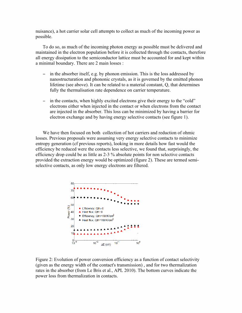
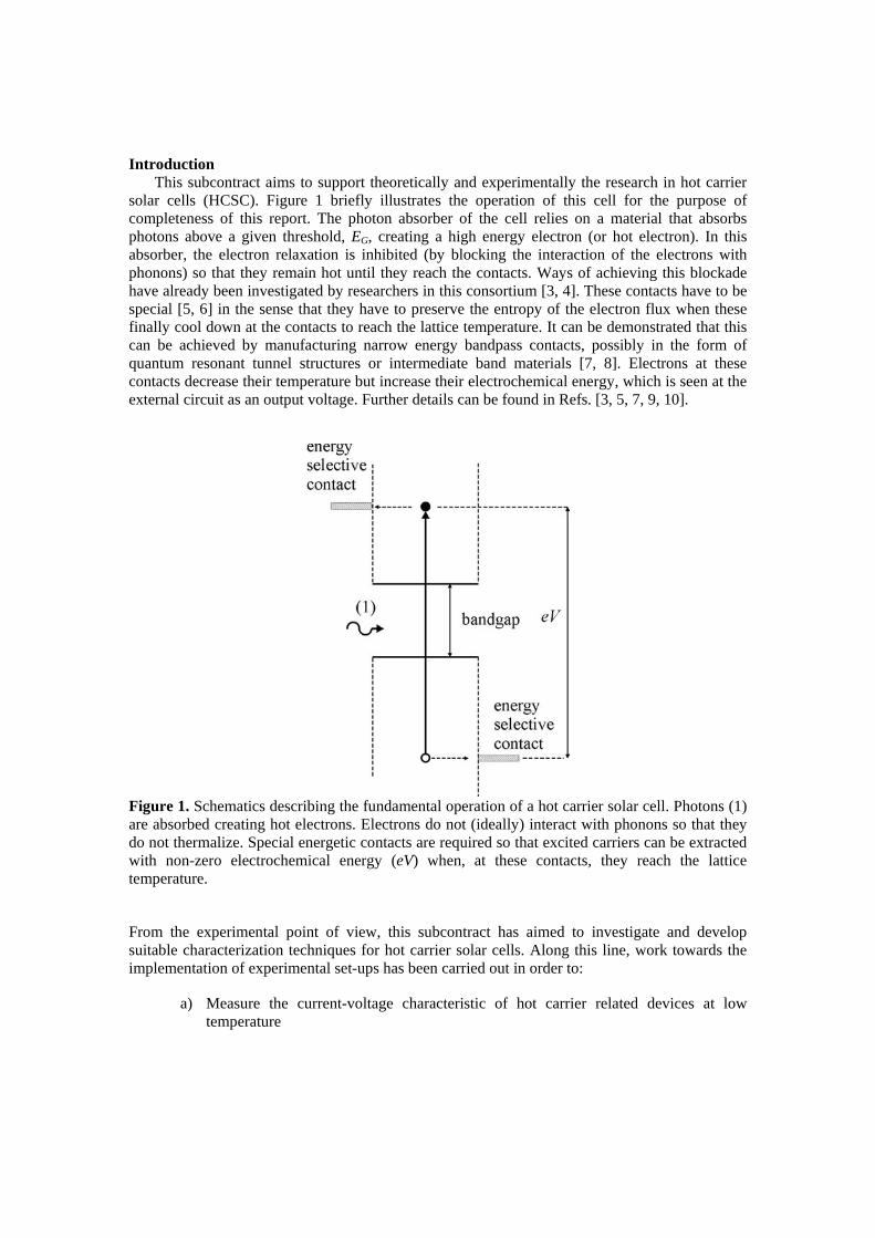
Background Hot carrier solar cells offer the possibility of very high efficiencies (limiting efficiency 68% for unconcentrated illumination) but with a structure that could be conceptually simple compared to other very high efficiency PV devices – such as multi-junction monolithic tandem cells. For this reason, the approach lends itself to ‘thin film’ deposition techniques, with their attendant low costs in materials and energy usage and facility to use abundant, non-toxic elements. [1-5] The Hot Carrier cell device has the following stringent requirements: A. Slowing of thermalisation of
photogenerated electrons (and holes) in the absorber material.
B. Extraction of these ‘hot carriers’ to external contacts over a narrow range of energies, such that excess carrier energy is not lost to the cold contacts.
C. In addition, a working device would require integration of the structures used to tackle A and B without compromising their performance.
The absorber has a hot carrier distribution at temp TH. Carriers cool isoentropically in the mono-energetic contacts to TA: their kinetic energy being converted into useable potential energy [1,2]. The difference of the Fermi levels of these two contacts manifests as a difference in chemical potential of the carriers at each contact and hence an external voltage. The challenges to produce such devices fall into 2 categories: (i) keeping carriers hot without heating the lattice and (ii) achieving a fast extraction of hot carriers through a narrow allowed energy range [1,2]. While these challenges are tough, it seems they can be met using newly available materials and more specifically nanostructured semiconductors. The absorber is conceptually a single layer, homogeneous on the scale of a complete device. Similarly contacts are conceptually relatively simple effectively 2D structures. This conceptual simplicity of construction of the whole device would lend itself to thin film or related techniques. A great strength of this project is that it synergistically combines the significant experience in all three generations of photovoltaics at the University of New South Wales (UNSW), with that on intermediate band cells and QD characterisation at References: [1] Green MA, “Third Generation Photovoltaics”, (Springer Verlag, 2003). [2] Würfel P, Sol Energy Mats & Sol Cells, 46(1997) 43. [3] Ross R and Nozik AJ, J. Appl Phys, 53 (1982) 3318. [4] Conibeer G et al, Solar Energy Materials and Solar Cells, 2009, 93, 713. [5] Guillemoles J-F et al, PVSEC (Shanghai, 2005) 375.
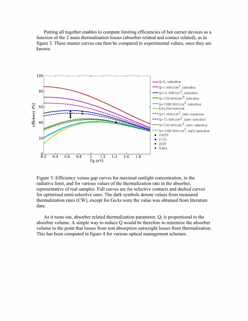
Instituto de Energia Solar (IES-UPM), with the pioneering work on Hot Carrier cells at IRDEP, Paris, in conjunction with UNSW and with the excellent optical expertise and facilities at Sydney University (USyd). Overview of Progress, September 2008 to August 2011 Progress towards both of the twin aims of developing a Hot Carrier absorber with slowed carrier cooling and characterising resonant tunnelling structures using quantum dots for energy selective contacts, has been made. Photogenerated hot carriers in an absorber lose their energy principally through emission of optical phonons. The subsequent blocking of the decay of these optical phonons by modification of an absorber material’s phonon dispersion maintains a ‘hot phonon’ population and reduces carrier cooling. Previous work in this project has shown this to be the optimal method to achieve slowed carrier cooling. Modelling of the efficiencies of hot carrier cells with indium nitride absorber has been carried out. The efficiencies of devices with non-ideal selective contacts has also been continued by both the UNSW and IRDEP nodes, with 3D modelling of double barrier contacts and of non-ideal contacts, which show efficiencies over 50% can be achievable and suggests that if Auger processes are weak the contacts only need be semi-selective. Fabrication and I-V characterisation of double barrier resonant tunnelling structures at UNSW with silicon nanostructures, have demonstrated improved resonance of energy at confined energy levels. Time resolved photoluminescence measurement of carrier cooling rates at the USyd and UNSW nodes has shown small increases in lifetimes of carriers in InN in addition to previously demonstrated slowed cooling in InP as compared to GaAs, demonstrating phonon bottleneck in wider phonon band gap materials. Further work at USyd on quantum well materials has shown long lifetimes of 2ns for hot carriers, corroborating earlier work and illuminating the mechanisms for slowing of carrier cooling. Modelling of nanostructure phononic properties has been used for real III-V nanostructures. Such structures have been fabricated by collaborators and are now being measured. Also colloidal quantum dot arrays have been fabricated at UNSW and are also now being measured for phonon dispersion. Modeling of the slowed cooling in MQW systems has identified several potential mechanisms to explain this slowed cooling, all of which enhance the phonon bottleneck effect. Device structures for complete devices are now being designed. These incorporate both the demonstrated slowed carried cooling of multiple nano-well structures and the phonon decay blocking of wide phononic band gap materials. Initial structures for real devices are now being grown based on multiple quantum wells with energy selective contacts. Further work will see further implementation and characterisation of these real device structures. It will also see consolidation of the nanostructure work and modelling of both III-V and colloidal nanostructures as well as quantum well structures. Energy selective contacts using double barrier structures will be further refined and used in combination with absorbers, with time resolved PL, Raman and I-V characterisation of carrier cooling and electrical properties, in order to demonstrate a complete hot carrier cell device.
Full descriptions of these projects are given in the following detailed reports from each of the UNSW, IRDEP and USyd nodes and a summary of the final report from 2010 of the IES-UPM node. Lists of papers published during the project are included at the end of each node report.
Project: “Hot Carrier solar cell: Implementation of the Ultimate PV Converter” Institution (node): University of New South Wales, Sydney, Australia Final Report April 2012 Abstract The UNSW node of the Hot Carrier Solar Cell project is investigating absorbers which slow the rate of carrier cooling - an essential element of a successful cell. It has also further developed the work on energy selective contacts for Hot Carrier cells. This work includes modelling the limiting efficiencies of cells using real material properties and modelling the phonon dispersions of ordered arrays of quantum dots. The object of the latter is to determine the potential to modify the allowed phonon energies such as to block the decay of optical phonons, this being the principle decay mechanism for hot photo-generated carriers in an absorber material. This will then offer the possibility of producing a material which substantially decreases the rate of carrier cooling in an absorber and hence allows carriers to be extracted whilst still hot and hence produce a higher external voltage. Thus also boosting the efficiency of such a ‘Hot Carrier solar cell’ very significantly. The investigation has four main themes: 1. Modelling of the phonon modified carrier cooling effects in quantum well and
quantum dot nanostructures. This allows the phonon properties of various material combinations to be modelled and assessed.
2. Calculating the limiting efficiencies of cells with specific electronic, and later with specific phononic properties.
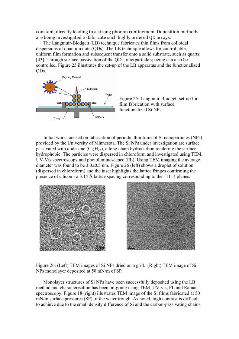
3. Fabrication and characterisation of ordered quantum dot arrays. Colloidal dispersion of capped nanocrystals to form 2D supercrystal arrays. These are being characterised for their modulation of phonon dispersions and for the effects of this modulation on the rate of carrier cooling.
4. Fabrication of double barrier resonant structures and characterising with illuminated I-V techniques.
Modelling on the efficiency of a Hot Carrier cell using indium nitride as an absorber has been carried out using real material parameters. Measurement of double barrier resonant quantum dot structures grown in high quality by collaborators and improved 2/3D modelling has been carried out. For absorbers, modelling of nanocrystals superlattice arrays has been applied to III-V QD superlattices. Such superlattices have been grown by collaborators and are being measured and colloidal Langmuir-Blodgett growth of silicon Si nanocrsystals arrays has been carried out. Measurement of carrier cooling rates has been carried out on indium nitride with its large phononic gap demonstrating the importance of material quality and comparisons made between III-V materials with similar electronic but different phononic band gaps. Materials have been identified suitable for absorbers and an analysis of analogues of these materials that use abundant elements carried out. The role of quantum well nanostructures in slowing carrier cooling has been investigated further. Finally design of complete hot carrier cell structures has been initiated with the important properties defined more precisely, with plans for fabricating such structures now being implemented.
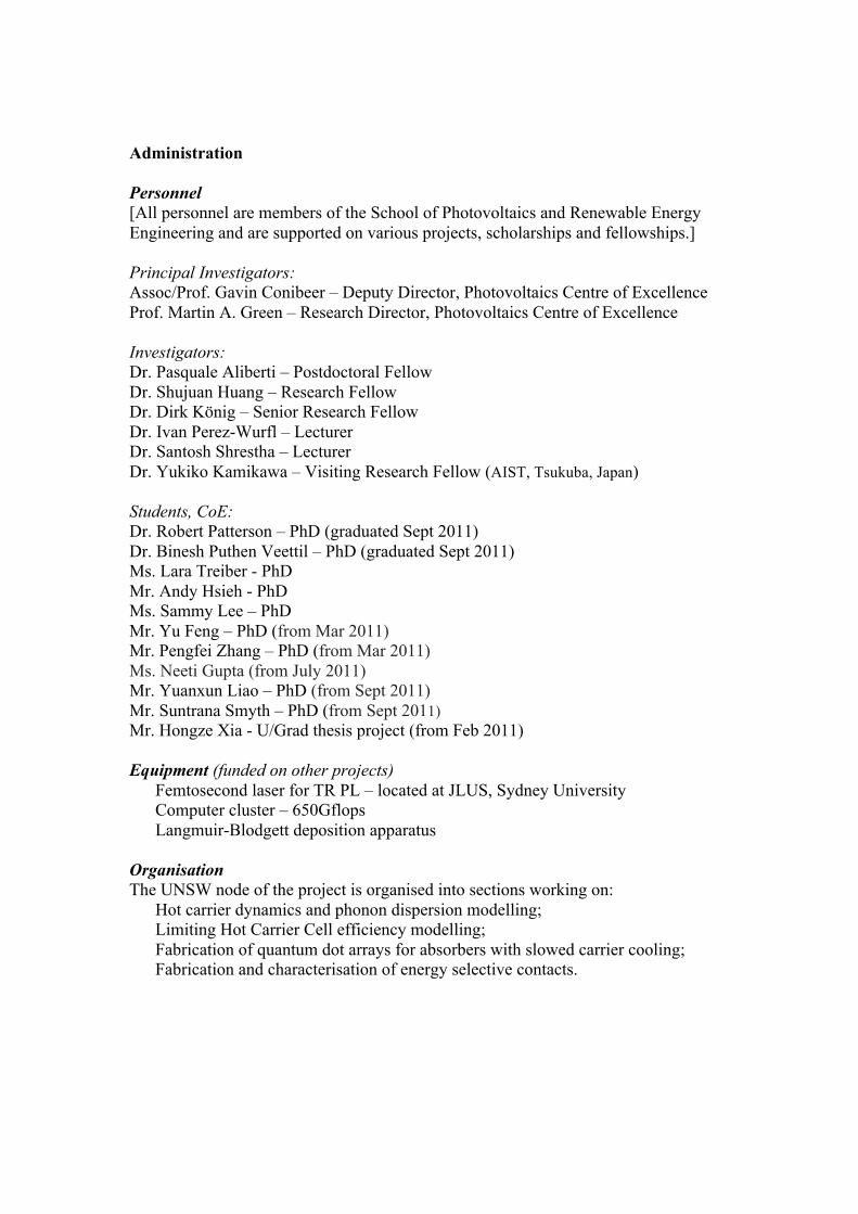
Administration Personnel [All personnel are members of the School of Photovoltaics and Renewable Energy Engineering and are supported on various projects, scholarships and fellowships.] Principal Investigators: Assoc/Prof. Gavin Conibeer – Deputy Director, Photovoltaics Centre of Excellence Prof. Martin A. Green – Research Director, Photovoltaics Centre of Excellence Investigators: Dr. Pasquale Aliberti – Postdoctoral Fellow Dr. Shujuan Huang – Research Fellow Dr. Dirk König – Senior Research Fellow Dr. Ivan Perez-Wurfl – Lecturer Dr. Santosh Shrestha – Lecturer Dr. Yukiko Kamikawa – Visiting Research Fellow (AIST, Tsukuba, Japan) Students, CoE: Dr. Robert Patterson – PhD (graduated Sept 2011) Dr. Binesh Puthen Veettil – PhD (graduated Sept 2011) Ms. Lara Treiber - PhD Mr. Andy Hsieh - PhD Ms. Sammy Lee – PhD Mr. Yu Feng – PhD (from Mar 2011) Mr. Pengfei Zhang – PhD (from Mar 2011) Ms. Neeti Gupta (from July 2011) Mr. Yuanxun Liao – PhD (from Sept 2011) Mr. Suntrana Smyth – PhD (from Sept 2011) Mr. Hongze Xia - U/Grad thesis project (from Feb 2011) Equipment (funded on other projects) Femtosecond laser for TR PL – located at JLUS, Sydney University Computer cluster – 650Gflops Langmuir-Blodgett deposition apparatus Organisation The UNSW node of the project is organised into sections working on:
Hot carrier dynamics and phonon dispersion modelling; Limiting Hot Carrier Cell efficiency modelling; Fabrication of quantum dot arrays for absorbers with slowed carrier cooling;
Fabrication and characterisation of energy selective contacts.
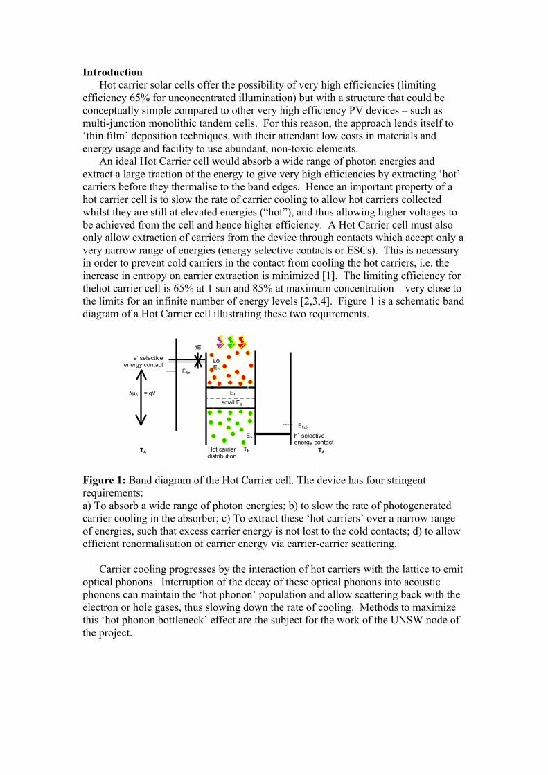
Introduction Hot carrier solar cells offer the possibility of very high efficiencies (limiting efficiency 65% for unconcentrated illumination) but with a structure that could be conceptually simple compared to other very high efficiency PV devices – such as multi-junction monolithic tandem cells. For this reason, the approach lends itself to ‘thin film’ deposition techniques, with their attendant low costs in materials and energy usage and facility to use abundant, non-toxic elements. An ideal Hot Carrier cell would absorb a wide range of photon energies and extract a large fraction of the energy to give very high efficiencies by extracting ‘hot’ carriers before they thermalise to the band edges. Hence an important property of a hot carrier cell is to slow the rate of carrier cooling to allow hot carriers collected whilst they are still at elevated energies (“hot”), and thus allowing higher voltages to be achieved from the cell and hence higher efficiency. A Hot Carrier cell must also only allow extraction of carriers from the device through contacts which accept only a very narrow range of energies (energy selective contacts or ESCs). This is necessary in order to prevent cold carriers in the contact from cooling the hot carriers, i.e. the increase in entropy on carrier extraction is minimized [1]. The limiting efficiency for thehot carrier cell is 65% at 1 sun and 85% at maximum concentration – very close to the limits for an infinite number of energy levels [2,3,4]. Figure 1 is a schematic band diagram of a Hot Carrier cell illustrating these two requirements.
Figure 1: Band diagram of the Hot Carrier cell. The device has four stringent requirements: a) To absorb a wide range of photon energies; b) to slow the rate of photogenerated carrier cooling in the absorber; c) To extract these ‘hot carriers’ over a narrow range of energies, such that excess carrier energy is not lost to the cold contacts; d) to allow efficient renormalisation of carrier energy via carrier-carrier scattering. Carrier cooling progresses by the interaction of hot carriers with the lattice to emit optical phonons. Interruption of the decay of these optical phonons into acoustic phonons can maintain the ‘hot phonon’ population and allow scattering back with the electron or hole gases, thus slowing down the rate of cooling. Methods to maximize this ‘hot phonon bottleneck’ effect are the subject for the work of the UNSW node of the project.
δE
LO ES
small Eg
Ef(n
)
Ef(p)
TA
h+ selective energy contact
Ef
ΔµA = qV
Hot carrier distribution
TH TA
e- selective energy contact
ES
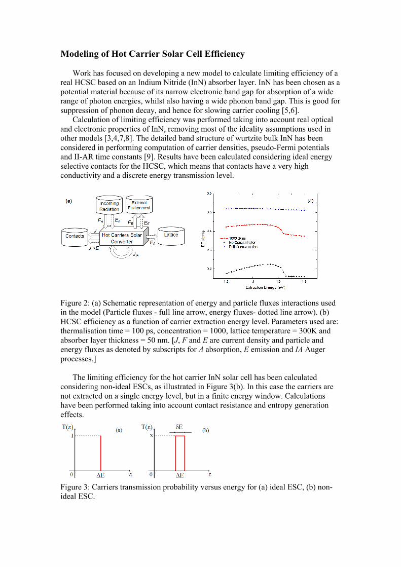
Modeling of Hot Carrier Solar Cell Efficiency Work has focused on developing a new model to calculate limiting efficiency of a real HCSC based on an Indium Nitride (InN) absorber layer. InN has been chosen as a potential material because of its narrow electronic band gap for absorption of a wide range of photon energies, whilst also having a wide phonon band gap. This is good for suppression of phonon decay, and hence for slowing carrier cooling [5,6]. Calculation of limiting efficiency was performed taking into account real optical and electronic properties of InN, removing most of the ideality assumptions used in other models [3,4,7,8]. The detailed band structure of wurtzite bulk InN has been considered in performing computation of carrier densities, pseudo-Fermi potentials and II-AR time constants [9]. Results have been calculated considering ideal energy selective contacts for the HCSC, which means that contacts have a very high conductivity and a discrete energy transmission level.
Figure 2: (a) Schematic representation of energy and particle fluxes interactions used in the model (Particle fluxes - full line arrow, energy fluxes- dotted line arrow). (b) HCSC efficiency as a function of carrier extraction energy level. Parameters used are: thermalisation time = 100 ps, concentration = 1000, lattice temperature = 300K and absorber layer thickness = 50 nm. [J, F and E are current density and particle and energy fluxes as denoted by subscripts for A absorption, E emission and IA Auger processes.] The limiting efficiency for the hot carrier InN solar cell has been calculated considering non-ideal ESCs, as illustrated in Figure 3(b). In this case the carriers are not extracted on a single energy level, but in a finite energy window. Calculations have been performed taking into account contact resistance and entropy generation effects.
Figure 3: Carriers transmission probability versus energy for (a) ideal ESC, (b) non-ideal ESC.
The flux of current travelling through the ESCs towards the cold metal electrodes can be described using the following relation.
( ) ( ), ,, , , , 3
min 0 0
( ) ( )z
C e h rt e h
y ze h e h T T V y z
y z
dk dkeJ T f f d dd d
ε εε
µε
ε ε ε ε ε επ ε ε
−⎛ ⎞⎡ ⎤= ⋅ − ⋅ ⎜ ⎟⎣ ⎦ ⎜ ⎟
⎝ ⎠∑ ∫ ∫h (1)
The current density in this case is proportional to the occupation probability at the
two sides of the ESC. Equation (1) has been derived assuming no correlation of energy of electrons in three different directions as shown in (2). This assumption is acceptable if there is a parabolic dispersion relation at minimum energy point along the three different directions.
zkykxkkzyx zyxzyx
++=++= ;εεεε (2) Based on energy and carrier conservation, Δµ and TC at steady state are
calculated.
0;0 =−−−=−+−eEEEE
eJFFF J
THEAIAEA (3)
[quantities as defined in Figure 2(a).]
Figure 4: (a) HCSC efficiency as a function of extraction width of ESCs for different extraction energies ΔE. (b) HCSC efficiency as a function of extraction energy ΔE for different ESCs energy width. Thermalisation time is 100 ps, lattice temperature is 300 K. Absorber layer thickness is 50 nm.
The maximum efficiency has been found for a ΔE between 1.15 eV and 1.2 eV with a transmission energy window δE of 0.02 eV. The value of limiting efficiency is 9.6% compared to 43.6% calculated in the previous section using ideal ESCs. The drop in efficiency is mostly due to the decrease of open circuit voltage related to the decreased extraction level, equation (3). This is partially compensated by an increase in extracted current due to increased II rate.
Figure 4 (a) shows calculated efficiency as a function of for several values of extraction energy. In all the curves two different trends can be identified. If the value of δE is too close to zero, the efficiency is very low due to low carrier extraction, thus a very small value of short circuit current. The conductivity of the contact in this case is indefinitely large. Enlarging δE, the number of carriers available for extraction increases, improving JSC, and so the maximum efficiency. In general the efficiency peak has been found for values of δE from 0.02 eV to 0.1 eV depending on the extraction energy ΔE. For the configurations which show higher efficiencies, ΔE <
1.35 eV, the optimum value of δE goes from 0.02 eV to 0.05 eV. This optimum value for δE of between is very close to kTRT. This represents the variation in energy in the contacts such that approximately the kTRT will inevitably be lost anyway by carriers thermalising within the contacts. Thus it sets a lower limit on a reasonable δE. Therefore this result indicates that the transmission energy range has to be very small and confirms once again the high selectivity requirements of ESCs for HCSC [10].
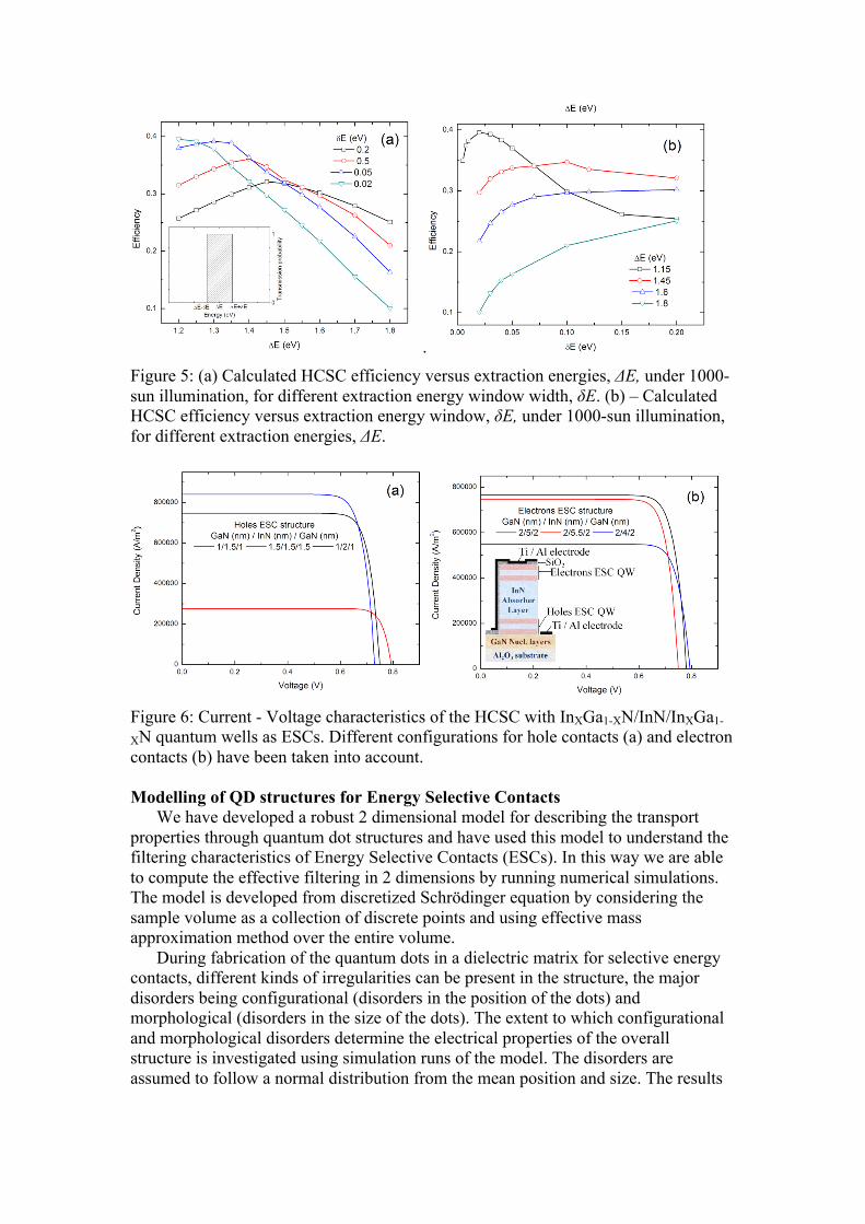
In Figure 4 (b) the value of maximum efficiency as a function of ΔE is reported for different values of δE. It can be observed that for small transmission energy window the extraction energy which allows maximum efficiency is lower compared to the one calculated using ideal ESCs. This effect is related to the higher occupancy at lower energies, which increases the value of JSC for contacts with a small transmission window. Energy Selective Contacts The requirement for a narrow range of contact energies can be met by an energy selective contact (ESC) based on double barrier resonant tunnelling. Tunnelling to the confined energy levels in a quantum dot layer embedded between two barrier layers, can give a conductance sharply peaked at the line up of the Fermi level on the ‘hot’ absorber side of the contact with the QD confined energy level. Conductance both below this energy and above it should be very significantly lower. This is the basis of the work carried out on double barrier resonant tunnelling ESCs. Modelling of InGaN/InN/InGaN double barrier resonant tunneling contacts Modeling and computation of HCSC efficiencies with non-ideal selective energy contacts has been carried out. [11] These are contacts extracting electrons at one side and holes at the other side with a narrow transmission window. Normally selective energy contacts are proposed to be realized with resonant tunneling diodes, since this structure gives confined energy levels, at which the transmission probability peaks. The transmission probabilities, as a function of energy levels, are modeled with one-dimensional quantum transmission treatment. The resultant transmission probabilities are involved in the device model, by relating the carrier statistics inside the absorber to the currents, i.e. carrier current and heat current thought the contacts. By equating the incoming and outgoing fluxes current corresponding to a given voltage is obtained, resulting in a MPP efficiency. From the computation the optimal efficiency is close to 40% for an InN absorber assuming complete optical absorption, even with a specific contact configuration. The contact configuration proposed is InGaN/InN/InGaN resonant tunneling diode, with the advantage of uniform nitride deposition with the absorber. Also variation of indium fraction gives an extra dimension to optimize the transmission peaks, leading to good cell performance. The results are shown in Figures 5 and 6.
. Figure 5: (a) Calculated HCSC efficiency versus extraction energies, ΔE, under 1000-sun illumination, for different extraction energy window width, δE. (b) – Calculated HCSC efficiency versus extraction energy window, δE, under 1000-sun illumination, for different extraction energies, ΔE.
Figure 6: Current - Voltage characteristics of the HCSC with InXGa1-XN/InN/InXGa1-
XN quantum wells as ESCs. Different configurations for hole contacts (a) and electron contacts (b) have been taken into account. Modelling of QD structures for Energy Selective Contacts We have developed a robust 2 dimensional model for describing the transport properties through quantum dot structures and have used this model to understand the filtering characteristics of Energy Selective Contacts (ESCs). In this way we are able to compute the effective filtering in 2 dimensions by running numerical simulations. The model is developed from discretized Schrödinger equation by considering the sample volume as a collection of discrete points and using effective mass approximation method over the entire volume. During fabrication of the quantum dots in a dielectric matrix for selective energy contacts, different kinds of irregularities can be present in the structure, the major disorders being configurational (disorders in the position of the dots) and morphological (disorders in the size of the dots). The extent to which configurational and morphological disorders determine the electrical properties of the overall structure is investigated using simulation runs of the model. The disorders are assumed to follow a normal distribution from the mean position and size. The results
show the outcome of an average of 1000 simulation runs with different standard deviation (σ) values.
Figure 7: Peak at 1.205eV of the conductance vs. energy plot for different values of σ for configurational disorder (left). Conductance vs. energy plot with peak at 1.573 eV for different values of σ for morphological disorder (right). Conductance given in units of 2e2/h. Figure 7 shows the simulation results for resonance in 2.6nm Si dot in SiO2 matrix under different orders of configurational disorders. As the disorders increases from σ =0 to σ =1 the conductance decreases by 53%, but the resonant energy remains the same at 1.205eV. This shows the confined energy in the QDs does not change as their size is fixed but the effective filtering reduces dramatically. Figure 7 shows the simulation results for a 2.2 nm Si dot in a SiO2 matrix under different orders of morphological disorders. As the disorder increases from σ =0 to σ = 1, the conductance decreases by 60% and the resonant peak remains the same at 1.573eV. But the morphological disorders cause major impact compared to configurational disorders because of the widening of the energy selection window. This is due to the distribution in size of the QDs, since QDs with different sizes have different resonant energies which are slightly different from the mean resonant energy, the average of them all increase the spread of the resonant peak and thus reducing the efficiency of the double barrier structure as energy selective contacts.
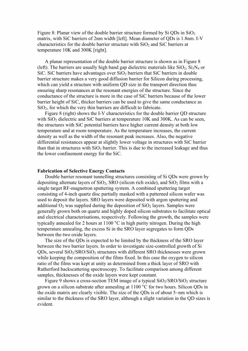
Figure 8: Planar view of the double barrier structure formed by Si QDs in SiO2 matrix, with SiC barriers of 2nm width [left]. Mean diameter of QDs is 1.8nm. I-V characteristics for the double barrier structure with SiO2 and SiC barriers at temperature 10K and 300K [right]. A planar representation of the double barrier structure is shown as in Figure 8 (left). The barriers are usually high band gap dielectric materials like SiO2, Si3N4 or SiC. SiC barriers have advantages over SiO2 barriers that SiC barriers in double barrier structure makes a very good diffusion barrier for Silicon during processing, which can yield a structure with uniform QD size in the transport direction thus ensuring sharp resonances at the resonant energies of the structure. Since the conductance of the structure is more in the case of SiC barriers because of the lower barrier height of SiC, thicker barriers can be used to give the same conductance as SiO2, for which the very thin barriers are difficult to fabricate. Figure 8 (right) shows the I-V characteristics for the double barrier QD structure with SiO2 dielectric and SiC barriers at temperature 10K and 300K. As can be seen, the structures with SiC potential barriers have higher current density at both low temperature and at room temperature. As the temperature increases, the current density as well as the width of the resonant peak increases. Also, the negative differential resistances appear at slightly lower voltage in structures with SiC barrier than that in structures with SiO2 barrier. This is due to the increased leakage and thus the lower confinement energy for the SiC. Fabrication of Selective Energy Contacts Double barrier resonant tunnelling structures consisting of Si QDs were grown by depositing alternate layers of SiO2, SRO (silicon rich oxide), and SiO2 films with a single target RF-magnetron sputtering system. A combined sputtering target consisting of 4-inch quartz disc partially masked with a patterned silicon wafer was used to deposit the layers. SRO layers were deposited with argon sputtering and additional O2 was supplied during the deposition of SiO2 layers. Samples were generally grown both on quartz and highly doped silicon substrates to facilitate optical and electrical characterisations, respectively. Following the growth, the samples were typically annealed for 2 hours at 1100 °C in high purity nitrogen. During the high temperature annealing, the excess Si in the SRO layer segregates to form QDs between the two oxide layers. The size of the QDs is expected to be limited by the thickness of the SRO layer between the two barrier layers. In order to investigate size-controlled growth of Si QDs, several SiO2/SRO/SiO2 structures with different SRO thicknesses were grown while keeping the composition of the films fixed. In this case the oxygen to silicon ratio of the films was kept at unity as determined from a thick layer of SRO with Rutherford backscattering spectroscopy. To facilitate comparison among different samples, thicknesses of the oxide layers were kept constant. Figure 9 shows a cross-section TEM image of a typical SiO2/SRO/SiO2 structure grown on a silicon substrate after annealing at 1100 °C for two hours. Silicon QDs in the oxide matrix are clearly visible. The size of the QDs is of about 5~nm which is similar to the thickness of the SRO layer, although a slight variation in the QD sizes is evident.
Figure 9: Typical TEM image of a SRO layer in SiO2 matrix after annealing at 1100 °C. Si QDs are clearly visible. For the investigation of size-controlled growth of QDs, several samples consisting of single layer Si QDs in SiO2 matrix were prepared. The SRO layer thicknesses were in the range of 1.8 nm to 7 nm. Thicknesses of the oxide layers were about 6 nm for all the samples, except for the two samples with SRO layer thickness of 1.8 nm and 2.4 nm. For these samples a 30 nm capping oxide layer was deposited to prevent possible oxidation of the QD layer during the high temperature annealing. For comparison, all the structures were grown with the same sputtering target and under similar growth conditions. Figure 10(a) shows results of room temperature PL measurements on several samples and Figure 10(b) shows the PL peak energy, derived from Figure 10(a), as a function of the respective QD sizes. It should be noted that no distinct PL signature were observed from as-deposited samples. The signal-to-noise ratio is quite good, although PL is measured on a single layer of Si QDs, demonstrating a strong absorption by Si QDs. This ratio is similar for the samples with SRO layer thickness greater than 3 nm, however it is relatively weaker for the sample with smaller SRO layer thicknesses. A strong decrease in PL intensity for samples containing smaller nanocrystals is reported in the literature. This is attributed to a decrease in the density of nanocrystals and the smaller absorption cross section [12,13]. These could also explain the relatively weaker PL signal from our samples containing smaller QDs.
Figure 10: (a) Results of PL measurements on a series of samples with a single layer of Si QDs in SiO2 matrix. (b) PL peak energy as a function of QD diameter. The solid curve is the best fit of PL energy with inverse square of QD diameter. For comparison data from selected literature are shown [12,14,15,16].
The full width at half maximum of the PL peaks are quite broad (> 0.25 eV) suggesting a large size distribution of QDs in the samples. This is consistent with the TEM images where a slight variation in QD sizes has been observed. Large distributions of size of nanocrystals in multilayered structure or bulk film have also been reported [12,14,15] and these are in reasonable agreement with our data (Figure 10(b)). However, PL peaks from different samples are clearly separated which demonstrates that the average sizes of QDs are different for different samples. Importantly, a blue-shift of the PL peak is observed with the decrease in the SRO layer thickness. The shift is larger for the smaller QDs whereas it is smaller for the bigger QDs which is consistent with the quantum confinement model. This is a significant result which shows that the size of a single layer of quantum dots can be controlled with the SRO layer thickness. The solid curve in (Figure 10(b)) is a best fit of PL peak energy with inverse square of QD diameter which is in good agreement with the data, both our own and those of other workers. Our data is also consistent with data for Si QDs in multilayered structure (SiO2/Si QDs/ SiO2/...Si QDs/SiO2), because it is grown with a similar technique, [16]. This may indicate that Si QDs in single and multilayered structures have similar optical properties. Annealing time and quantum dot formation The double barrier structures are typically annealed for two hours at 1100°C for QDs formation. In order to investigate the optimum annealing duration, two sets of samples, one set with SRO thickness of 3.6 nm and another set with SRO thickness of 6 nm, were grown under similar conditions. Figure 11 shows PL peak energy for two sets of samples as a function of annealing time. The annealing time indicated in the diagram refers to the duration at 1100 °C (the ramping up and ramping down time are not included).
Figure 11: PL peak energy as a function of annealing time. It is evident that PL signals can be observed even after a short anneal. Interestingly, there is virtually no decrease in the PL energy peaks when samples were annealed for longer, as would be expected if the QDs sizes were increasing with annealing time. This suggests that the formation of QDs saturates and attains a mean diameter after a few minutes of annealing at 1100°C. Further annealing, in general, results in increase in the PL intensity, as also seen in [17]. Enhancement in the PL
intensity is suggested to be due mainly to the passivation of Si dangling bonds at the Si-SiO2 interfaces caused by the longer anneal. Summary of work on ESCs A robust model for analysing deviations from an ideal resonant tunnelling structure has been developed. This has been used to model hot carrier cell efficiencies and selected energies for both quantum dot and InGaN/In?InGaN double barrier resonant tunneling structures. With good selection predicted for good quality structures. The effect of contact width on efficiency has been modeled and seems to have a strong detrimental effect at values greater than kT, although this effect is reduced for high selected energies because the occupancy of these carrier energies will be lower. The effects of disorder of QD size and position have also been modeled and show a very strong effect on selection of the former but a much weaker effect of the latter. Experimental work has focused on SiO2/Si-QD/SiO2 double barrier resonant tunneling structures. Improvement in the Si QD layer size uniformity with improved control over the QD size and size distribution has been demonstrated. Data similar to multilayer QD samples are seen, except that size control can be controlled by annealing time, with longer times giving improved QD surface passivation. Future work will focus on the quality of the oxide and other double barrier layer materials. Improvement of quality here will be important to realise good energy selection.
Hot Carrier Absorbers: slowing of carrier cooling Carrier cooling in a semiconductor proceeds predominantly by carriers scattering their energy with optical phonons. This builds up a non-equilibrium ‘hot’ population of optical phonons which, if it remains hot, will drive a reverse reaction to re-heat the carrier population, thus slowing further carrier cooling. This is known as the ‘phonon bottleneck’ effect, and its enhancement is the principal mechanism investigated to slow carrier cooling. This enhancement can be achieved in a number of ways, most of which appear to be independent of each other and hence potentially more than one can be incorporated in the same material or structure. (1) Prevention or slowing of the diffusion of hot carriers in the material will maintain localized hot spots of carriers and result in an uneven distribution of emitted optical phonons. This will enhance the phonon bottleneck locally, which in turn will lead to an overall higher carrier temperature because the phonon bottleneck is non-linear. (2) Scattering or reflection of optical phonons emitted by hot carriers in the structure will maintain localized non-equilibrium hot phonon populations and again lead to a greater phonon bottleneck. (3) Optical phonons decay by emitting acoustic phonons with increasing distribution of heat and entropy in the material. Prevention of these optical phonon decays using materials with large phonon band gaps will slow this process and enhance phonon bottleneck. (4) Folding of acoustic phonon modes in a coherent nanostructure will lead to forbidden phonon energies and to a reduction in potential acoustic phonon decay routes. Thus again restricting overall phonon decay and enhancing phonon bottleneck. These processes each deal with a separate aspect of loss of energy to phonons and are hence largely independent of each other. They also progress in the level of entropy increase and hence in their degree of irreversibility. It should be possible to design a structure able to exhibit more than one of these mechanisms and possibly all of them, thus maximizing the enhancement of phonon bottleneck and minimizing carrier cooling. Properties required of a Hot Carrier Absorber The work on absorbers presented below and earlier work allows the properties required for a good hot carrier absorber material to be determined. These are listed below in three categories and approximately in order of priority.
1 Good electronic properties: 1.1 Small electronic band gap (Eg) and a reasonably high DOS for all energies above
Eg – so as to allow a wide range of photon absorption. Eg should be less than 1eV. For 1 sun concentration the optimum is 0.7eV - as a band gap below this energy gives no advantage in the balance between absorption and emission. As the concentration ratio increases this optimum band gap decreases to zero at maximum concentration [2].
1.2 Good renormalisation rates in the material, i.e. good e-e and h-h scattering (e=electron, h=hole). This requires a reasonable DOS at all energies above Eg, or at least only very narrow gaps between energy levels, ≤ kT300K. This being similar to requirement 1.1. This in turn requires a good overlap of wavefunction for carriers through the material, i.e. poor electronic confinement or a reasonable conductor. This condition is met in all inorganic semiconductors quite easily, with e-e scattering rates of less than 100fs for reasonable carrier
concentrations. It may not be met in organic semiconductors or in nanostructures with large barrier heights.
1.3 Good carrier transport in order to allow transport of hot carriers to the contacts. This is similar to 1.2, except that it only need be in the direction of the contacts, probably the z growth direction. A reasonably low resistance is probably good.
2 A mechanism or mechanisms to enhance the ‘phonon bottleneck effect’: 2.1 Internal electronic barriers to prevent or reduce diffusion of hot carriers. Thus
maintaining a non-equilibrium carrier population in thin layers [18]. 2.2 Internal interfaces to enhance scattering of phonons but promote or not impede
transmission of electrons – ‘phonon glass / electron crystal’ as used for high thermoelectric figure of merit quantum well or nanostructured materials [18].
2.3 A small LO optical phonon energy (ELO). This reduces the amount of energy lost per LO phonon emission, requiring a greater number to be emitted for a given energy loss [19]. However, it is difficult to have both a small ELO and the large phononic gap required in 2.2. This condition requires further investigation, but does still argue for a small ELO.
2.4 Large phononic band gap (EO(min) - ELA)* - in order to suppress Klemens decay of optical phonons this must be at least as large as the maximum acoustic phonon energy. Hence a large mass difference (or large force constant difference) between constituent elements is required [20].
2.5 Narrow optical phonon energy dispersion (ELO - EO(min))* – in order to minimise the loss of energy to TO phonons by Ridley decay. This requires a high symmetry atomic or nano-structure, preferably cubic with degenerate optical phonon energies at zone centre.
2.6 An absolute small maximum acoustic phonon energy (ELA). This maximises the phononic gap if ELO is also small. A small ELA requires a large mass for the heavy atom and/or small force constant for its bonds.
3 Requirements for large scale implementation: 3.1 It should be possible to make good quality, highly ordered, low defect material.
Preferably it should be easy and cheap to do this. 3.2 Earth abundant and readily available and processable constituent elements and
processes. 3.3 No or low toxicity of elements, compounds and processes. Slowed carrier cooling in MQWs [18] Low dimensional multiple quantum well (MQW) systems have also been shown to have lower carrier cooling rates. Comparison of bulk and MQW materials has shown significantly slower carrier cooling in the latter. Figure 12 shows data for bulk GaAs as compared to MQW GaAs/AlGaAs materials as measured using time resolved transient absorption by Rosenwaks [21], recalculated to show effective carrier temperature as a function of carrier lifetime by Guillemoles [22]. It clearly shows that the carriers stay hotter for significantly longer times in the MQW samples, particularly at the higher injection levels by 1½ orders of magnitude. This is due to an enhanced ‘phonon bottleneck’ in the MQWs allowing the threshold intensity at which a certain ratio of LO phonon re-absorption to emission is reached which allows maintenance of a hot carrier population, to be reached at a much lower illumination
* ELO , EO(min) & ELA are the maximum optical, minimum optical and maximum acoustic phonon energies, respectively.
level. More recent work on strain balanced InGaAs/GaAsP MQWs by Hirst [23] has also shown carrier temperatures significantly above ambient, as measured by PL. Increase in In content to make the wells deeper and to reduce the degree of confinement is seen to increase the effective carrier temperatures.
Figure 12: Effective carrier temperature as a function of carrier lifetime for bulk GaAs as compared to GaAs/AlGaAs MQWs: time resolved transient absorption data for different injection levels, from Rosenwaks [21], recalculated by Guillemoles [22]. The mechanisms for the reduced carrier cooling rate in these MQW systems are not yet clear. However there are three effects that are likely to contribute. The first is that in bulk material photogenerated hot carriers are free to diffuse deeper into the material and hence to reduce the hot carrier concentration at a give depth. This will also decrease the density of LO phonons emitted by hot carriers as they cool and make a phonon bottleneck more difficult to achieve at a given illumination intensity. Whereas in a MQW there are physical barriers to the diffusion of hot carriers generated in a well and hence a much greater local concentration of carriers and therefore also of emitted optical phonons. Thus the phonon bottleneck condition is achieved at lower intensity [22]. The second effect is that for the materials systems which show this slowed cooling, there is very little or no overlap between the optical phonon energies of the well and barrier materials. For instance the optical phonon energy ranges for the GaAs wells and AlGaAs barriers used in [21] at 210-5285meV and 280-350meV, respectively, exhibit very little overlap in energy, with zero overlap for the zone centre LO phonon energies of 285 and 350meV [24]. Consequently the predominantly zone centre LO phonons emitted by carriers cooling in the wells will be reflected from the interfaces and will remain confined in the wells, thus enhancing the phonon bottleneck at a given illumination intensity. The latter hypothesis is supported by the evidence of significantly improved thermoelectric figures of merit (ZT) for superlattices of materials with very small barrier height but significant phonon energy mismatch. Such ‘phonon glass / electron crystal’ materials allow reasonable electronic transport but significant phonon scattering. Examples include metal nitride nano-well materials with a small conduction band offset in Zebarjadi et al. [25] and Si/Ge nano-well materials in Lee et al. [26]. Thirdly, if there is a coherent spacing between the nano-wells (as there is for these MQW or superlattice systems) a coherent Bragg reflection of phonon modes can be established which blocks certain phonon energies perpendicular to the wells, opening up one dimensional phononic band gaps [27]. For specific ranges of nano-well and barrier thickness these forbidden energies can be at just those energies required for
phonon decay. This coherent Bragg reflection should have an even stronger effect than the incoherent scattering of the second mechanism at preventing emission of phonons and phonon decay in the direction perpendicular to the nano-wells. Whilst this does depend on a specific and coherent nano-well array it does not require the nano-wells to be thin enough to be electronically quantized as such phonon dispersion folding occurs for any size of superstructure as long as it is coherent, (anechoic chambers and bridge bearings are macroscopic examples). It is likely that all three of these effects will reduce carrier cooling rates. None depend on electronic quantum confinement and hence should be exhibited in wells that are not thin enough to be quantized but are still quite thin (perhaps termed ‘nano-wells’). In fact it may well be that the effects are enhanced in such nano-wells as compared to full QWs due to the former’s greater density of states and in particular their greater ratio of density of electronic to phonon states which will enhance the phonon bottleneck for emitted phonons. The fact that it is the deeper and hence less confined wells in [23] which show higher carrier temperatures is reasonable evidence to support the hypothesis that nano-wells without quantum confinement are all that are required. Whist several other effects might well be present in these MQW systems, further work on variation of nano-well and barrier width and comparison between material systems, should be able to distinguish which of these reduced carrier diffusion, phonon confinement or phonon folding mechanisms might be dominant. Modelling of electron-phonon interactions: Another important factor is the Frohlich interactions between hot electrons and longitudinal optical phonon modes. The importance of investigating the fundamental particle interactions occurring in the device is demonstrated by the significant dependence between the carrier energy relaxation time and the output efficiency. The underlying mechanism of phonon bottleneck effect involves two parts, the first is the blocking of the Frohlich interaction between electrons and phonons; while the second is the blocking of phonon decay from the optical modes into acoustic modes. Also the build-up of non-equilibrium acoustic phonons may also contribute to reduced carrier energy relaxations. In order to understand the mechanism of slow relaxation rates in different types of materials the three interaction processes need to be simulated. The Frohlich interaction occurs in polar semiconductors and creates energy exchange between electrons and longitudinal phonons. It affects the total energy and state transition rates by an interaction Hamiltonian. The Frohlich interaction Hamiltonian for superlattice structures involves an overlap integral over one dimension (the direction perpendicular to planes). The derivation of the Hamiltonian involves the interaction between electrons and polarization fields induced by longitudinal mode vibrations. By obtaining the divergence of the polarization field an effective phonon envelope function is developed and incorporated in the overlap integral. In the multiple quantum well superlattice structure the zone-folded phonon modes are mainly confined only inside one type of layers, i.e. the barrier layers or the well layers, due to their different force constants and lattice constants. The separation of two types of longitudinal optical phonons gives very different interaction strengthes with electrons. For a quantum well structure with high barrier height the majority of electrons are confined inside well layers, which mainly interact with LO phonon modes confined also in the well layers. This could reduce the energy relaxations for two reasons. One is due to the weak interaction with the other type of phonons, while
the other is because the localized hot LO phonons need a longer time to decay into acoustic phonons, i.e. the phonon bottleneck effect, resulting in higher probability of energy being coupled back to electrons. While the separation of phonon and electron systems are empirically obtained with good accuracy, it has to be mentioned that the effective phonon envelope function has an exponential decay part in the other type of layers, even if the actual atomic vibration is strictly confined inside one type of layers. By assuming electrons and optical phonons are maintained in thermal equilibrium respectively, with certain temperatures, for instance electrons at 1000K and phonons at 300K, the energy relaxation rates from electrons to phonons are calculated, corresponding to different superlattice structures. Considering one-dimensional dispersions the calculated energy relaxation rates can be reduced in superlattice structures as compared to those in wurtzite-InN bulk material. For electrons at 1000K and phonons at 300K the energy relaxation time of electrons can be as long as 1ps, approximately 3 orders of magnitude longer than that in the bulk case. The other source of the phonon bottleneck effect comes from the blocking of optical phonon decay. Longitudinal optical modes can decay into longitudinal transverse modes or acoustic modes due to the anharmonicity of bond energies, which is well known as Klemens decay. To calculate the interaction rates the interaction Hamiltonian for Klemens decay needs to be figured out first. The out-of-phase atomic vibrations of optical modes indicate the Hamiltonian should depend on the atomic displacement, instead of the elastic strain which is related to the spatial derivative of atomic displacement. To calculate the overall carrier energy relaxation rates all the interaction processes need to be considered. Monte Carlo simulation on the electron and phonon systems provides a good approach to calculate the evolution of particle distributions, hence the energy relaxation figures. The whole evolution period is separated into small intervals. The dynamics of each type of interaction determines the transition probability during the short intervals. Random numbers are introduced to determine the state transitions according to the corresponding probabilities. For a certain amount of incoming energy flux, the steady-state particle distributions are to be determined after a long enough time period, and also a sufficient number of iterations. The results in Figures 13 and 14 include phonon dispersions from linear chain model, electron dispersions from superlattice Kronig-Penney model. Frohlich interaction strength and corresponding carrier energy relaxations are also calculated with the summation method under a Fermi-statistics approximation and Monte Carlo simulations. This is a problem requiring significant computational resources and computer time. At present this is unavailable, so temporary results have been calculated and are shown in Figures 13 and 14. Notice that all the computations can be done for any kind of device configuration, including well thickness, barrier thickness and Indium fraction in the barrier layer.
Figure 13: (Left) – Phonon dispersions for wavevectors perpendicular to the planar layers; (Right) – Atom vibrations of optical modes at the zone center (the bottom mode has the highest energy), i.e. phonon envelope functions
Figure 14: (Left) – Electron dispersions for wavevectors perpendicular to the planar layers; (Right) – Electron wavefunctions of states at the zone center (the bottom mode has the lowest energy) Optical Phonon decay Optical phonons lose their energy by decay into acoustic phonons, or heat in the lattice. The principal mechanism by which this can occur is the Klemens mechanism, in which the optical phonon decays into two acoustic phonons of half its energy and
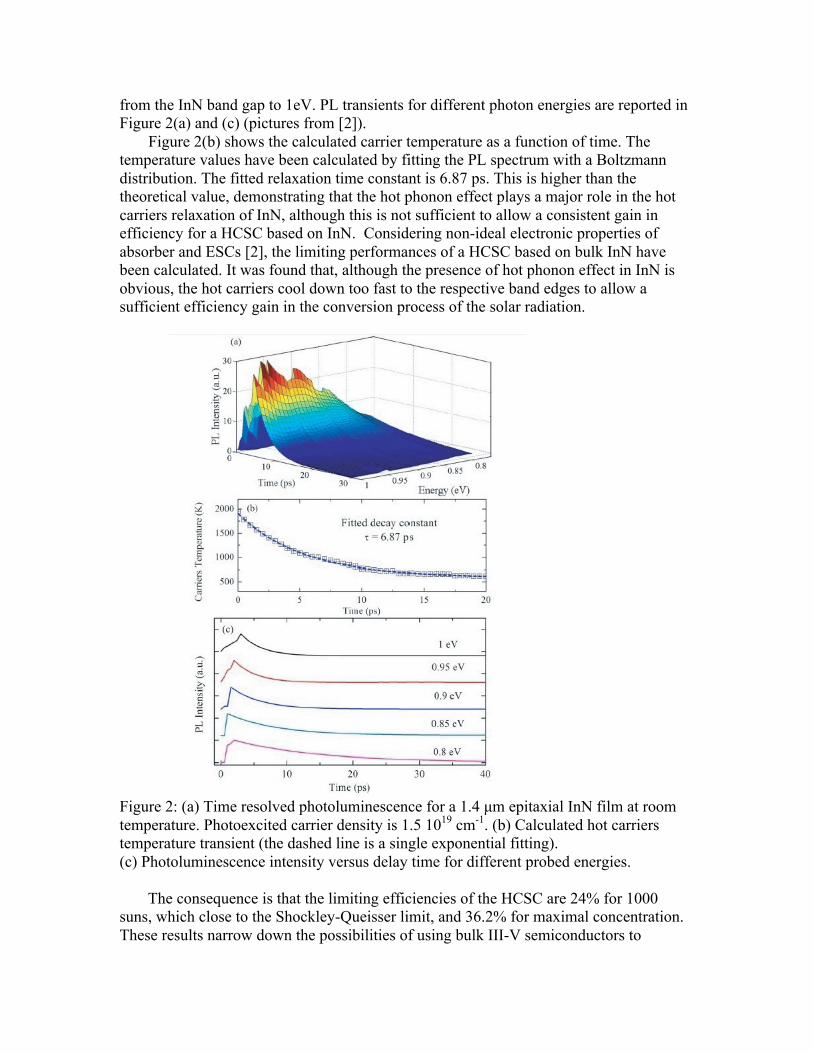
of equal and opposite momenta [28]. The build up of emitted optical phonons is strongly peaked at zone centre for polar compound semiconductors due to the Frölich interaction and rather less peaked at zone centre for non-polar elemental semiconductors due to the deformation potential interaction. The strong coupling of the Frölich interaction also means that high energy optical phonons are also constrained to near zone centre even if parabolicty of the bands is no longer valid [29]. This zone centre optical phonon population determines that the dominant optical phonon decay mechanism is this pure Klemens decay. Suppression of phonon decay in bulk materials In some bulk semiconductors, with a large difference in their anion and cation masses, there can be a large gap between the highest acoustic phonon energy and the lowest optical phonon energy, possibly large enough to block operation of this Klemens mechanism, which can be termed a ‘phononic band gap’. Work using a simple 1D force constant model [20] and complemented by high accuracy DFT computation [19] indicates that GaN, InN and InP all have large phononic band gaps, which are close to those found experimentally [30]. We are using time resolved photoluminescence (tr-PL) to investigate the carrier cooling rates in these materials. Time resolved photoluminescence measurements of bulk phononic band gap materials (with USyd node) The potential efficiency boost, which can be achieved by Hot Carrier solar cells, is directly related to the possibility of extracting high energy carriers from the absorber layer before thermalisation, increasing the voltage and hence the conversion efficiency. The poor conversion efficiency of photons with energies above the band gap of the absorber is the main loss mechanism in conventional single junction solar cells. The investigation of thermalisation time constants of hot carriers is a crucial step towards the engineering of Hot Carrier cells. The efficiency of an InN based hot carrier solar cell has been calculated using a complex theoretical model, (see section above on Hot Carrier cell efficiency modeling). It was found that the limiting efficiency is strongly related to hot carriers relaxation velocity in the absorber [9].
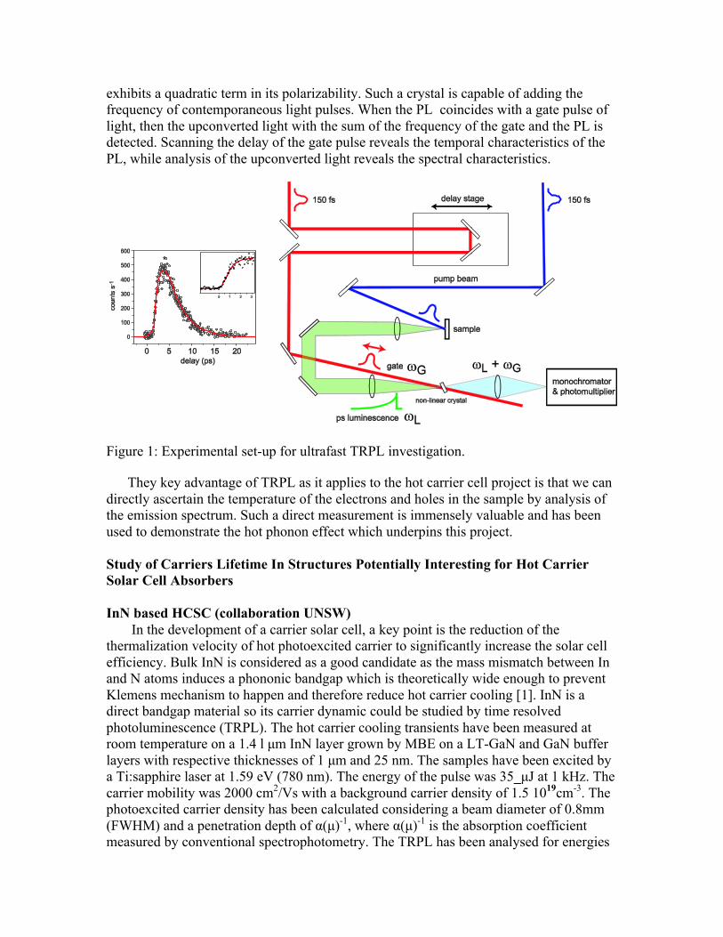
In a strong collaboration with the Sydney University (USyd) node, femtosecond time resolved photoluminescence (tr-PL) spectroscopy has been used to measure the carrier cooling rate in Indium nitride (InN). In N has a wide band gap between the optical and acoustic branches of its phonon dispersion relation [30]. The main mechanism for carrier energy thermalisation in InN is the interaction of highly energetic electrons and holes with LO phonons (as it is in most semiconductors) [31]. However the large phonon band gap means that Klemens decay of optical phonons into acoustic phonons should be suppressed. Thus allowing the optical phonon population to increase and enhances the “Hot Phonon” or “Phonon Bottleneck Effect” thus promoting the re-absorption of optical phonons and slowing carrier cooling [32].
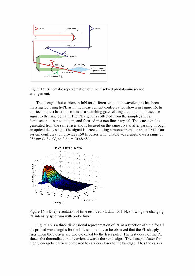
Figure 15: Schematic representation of time resolved photoluminescence arrangement.
The decay of hot carriers in InN for different excitation wavelengths has been investigated using tr-PL as in the measurement configuration shown in Figure 15. In this technique a laser pulse acts as a switching gate relating the photoluminescence signal to the time domain. The PL signal is collected from the sample, after a femtosecond laser excitation, and focused in a non linear crystal. The gate signal is generated from the same laser and is focused on the same crystal after passing through an optical delay stage. The signal is detected using a monochromator and a PMT. Our system configuration provides 150 fs pulses with tunable wavelength over a range of 256 nm (4.84 eV) to 2.6 µm (0.48 eV).
Figure 16: 3D representation of time resolved PL data for InN, showing the changing PL intensity spectrum with probe time.
Figure 16 is a three dimensional representation of PL as a function of time for all the probed wavelengths for the InN sample. It can be observed that the PL sharply rises when the carriers are photo-excited by the laser pulse. The fast decay of the PL shows the thermalisation of carriers towards the band edges. The decay is faster for highly energetic carriers compared to carriers closer to the bandgap. Thus the carrier
population quickly degenerates towards the band edges during the thermalisation process.
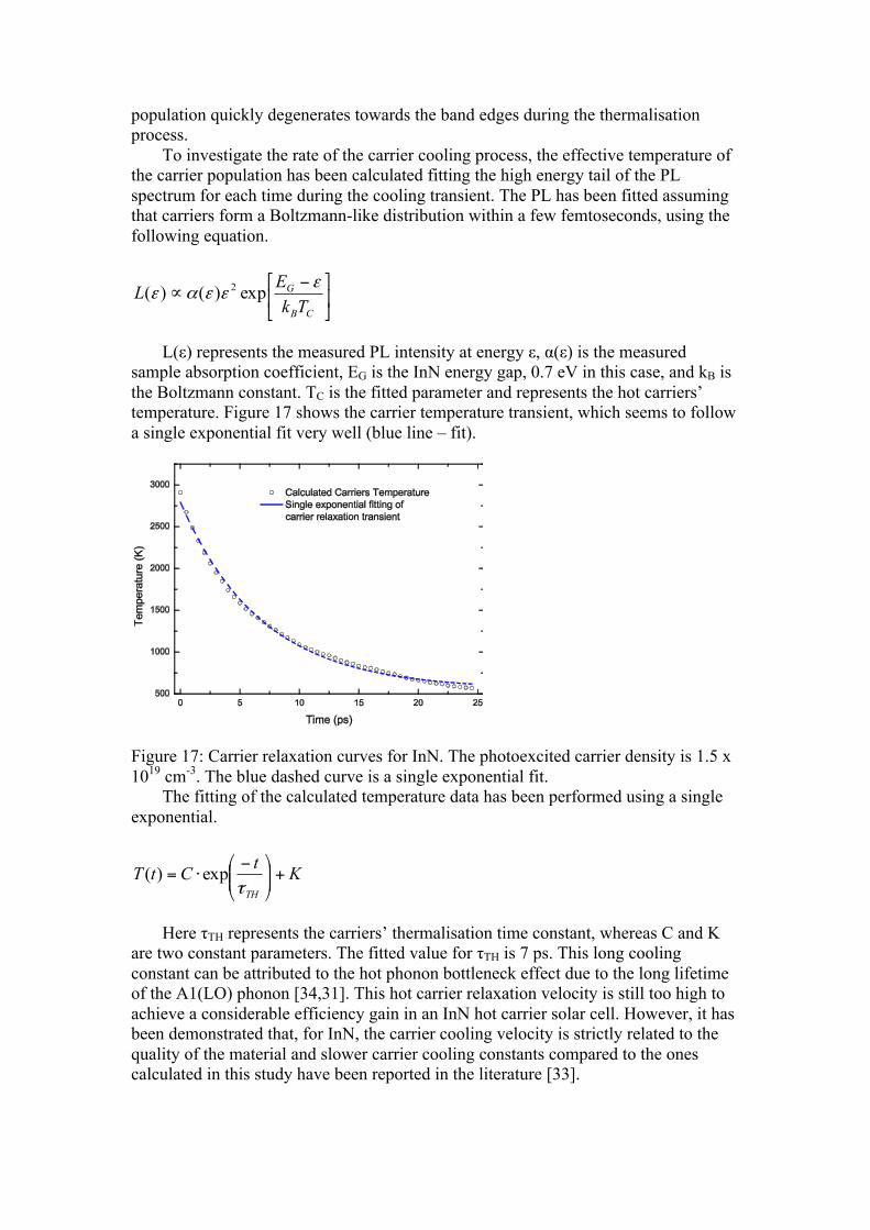
To investigate the rate of the carrier cooling process, the effective temperature of the carrier population has been calculated fitting the high energy tail of the PL spectrum for each time during the cooling transient. The PL has been fitted assuming that carriers form a Boltzmann-like distribution within a few femtoseconds, using the following equation.
⎥⎦
⎤⎢⎣
⎡ −∝
CB
G
TkEL ε
εεαε exp)()( 2
L(ε) represents the measured PL intensity at energy ε, α(ε) is the measured sample absorption coefficient, EG is the InN energy gap, 0.7 eV in this case, and kB is the Boltzmann constant. TC is the fitted parameter and represents the hot carriers’ temperature. Figure 17 shows the carrier temperature transient, which seems to follow a single exponential fit very well (blue line – fit).
Figure 17: Carrier relaxation curves for InN. The photoexcited carrier density is 1.5 x 1019 cm-3. The blue dashed curve is a single exponential fit.
The fitting of the calculated temperature data has been performed using a single exponential.
KtCtTTH
+⎟⎟⎠
⎞⎜⎜⎝
⎛ −⋅=
τexp)(
Here τTH represents the carriers’ thermalisation time constant, whereas C and K are two constant parameters. The fitted value for τTH is 7 ps. This long cooling constant can be attributed to the hot phonon bottleneck effect due to the long lifetime of the A1(LO) phonon [34,31]. This hot carrier relaxation velocity is still too high to achieve a considerable efficiency gain in an InN hot carrier solar cell. However, it has been demonstrated that, for InN, the carrier cooling velocity is strictly related to the quality of the material and slower carrier cooling constants compared to the ones calculated in this study have been reported in the literature [33].
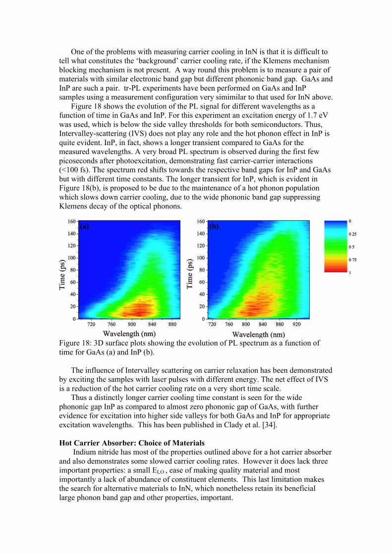
One of the problems with measuring carrier cooling in InN is that it is difficult to tell what constitutes the ‘background’ carrier cooling rate, if the Klemens mechanism blocking mechanism is not present. A way round this problem is to measure a pair of materials with similar electronic band gap but different phononic band gap. GaAs and InP are such a pair. tr-PL experiments have been performed on GaAs and InP samples using a measurement configuration very simimilar to that used for InN above. Figure 18 shows the evolution of the PL signal for different wavelengths as a function of time in GaAs and InP. For this experiment an excitation energy of 1.7 eV was used, which is below the side valley thresholds for both semiconductors. Thus, Intervalley-scattering (IVS) does not play any role and the hot phonon effect in InP is quite evident. InP, in fact, shows a longer transient compared to GaAs for the measured wavelengths. A very broad PL spectrum is observed during the first few picoseconds after photoexcitation, demonstrating fast carrier-carrier interactions (<100 fs). The spectrum red shifts towards the respective band gaps for InP and GaAs but with different time constants. The longer transient for InP, which is evident in Figure 18(b), is proposed to be due to the maintenance of a hot phonon population which slows down carrier cooling, due to the wide phononic band gap suppressing Klemens decay of the optical phonons.
Figure 18: 3D surface plots showing the evolution of PL spectrum as a function of time for GaAs (a) and InP (b). The influence of Intervalley scattering on carrier relaxation has been demonstrated by exciting the samples with laser pulses with different energy. The net effect of IVS is a reduction of the hot carrier cooling rate on a very short time scale. Thus a distinctly longer carrier cooling time constant is seen for the wide phononic gap InP as compared to almost zero phononic gap of GaAs, with further evidence for excitation into higher side valleys for both GaAs and InP for appropriate excitation wavelengths. This has been published in Clady et al. [34]. Hot Carrier Absorber: Choice of Materials
Indium nitride has most of the properties outlined above for a hot carrier absorber and also demonstrates some slowed carrier cooling rates. However it does lack three important properties: a small ELO , ease of making quality material and most importantly a lack of abundance of constituent elements. This last limitation makes the search for alternative materials to InN, which nonetheless retain its beneficial large phonon band gap and other properties, important.
Analogues of InN
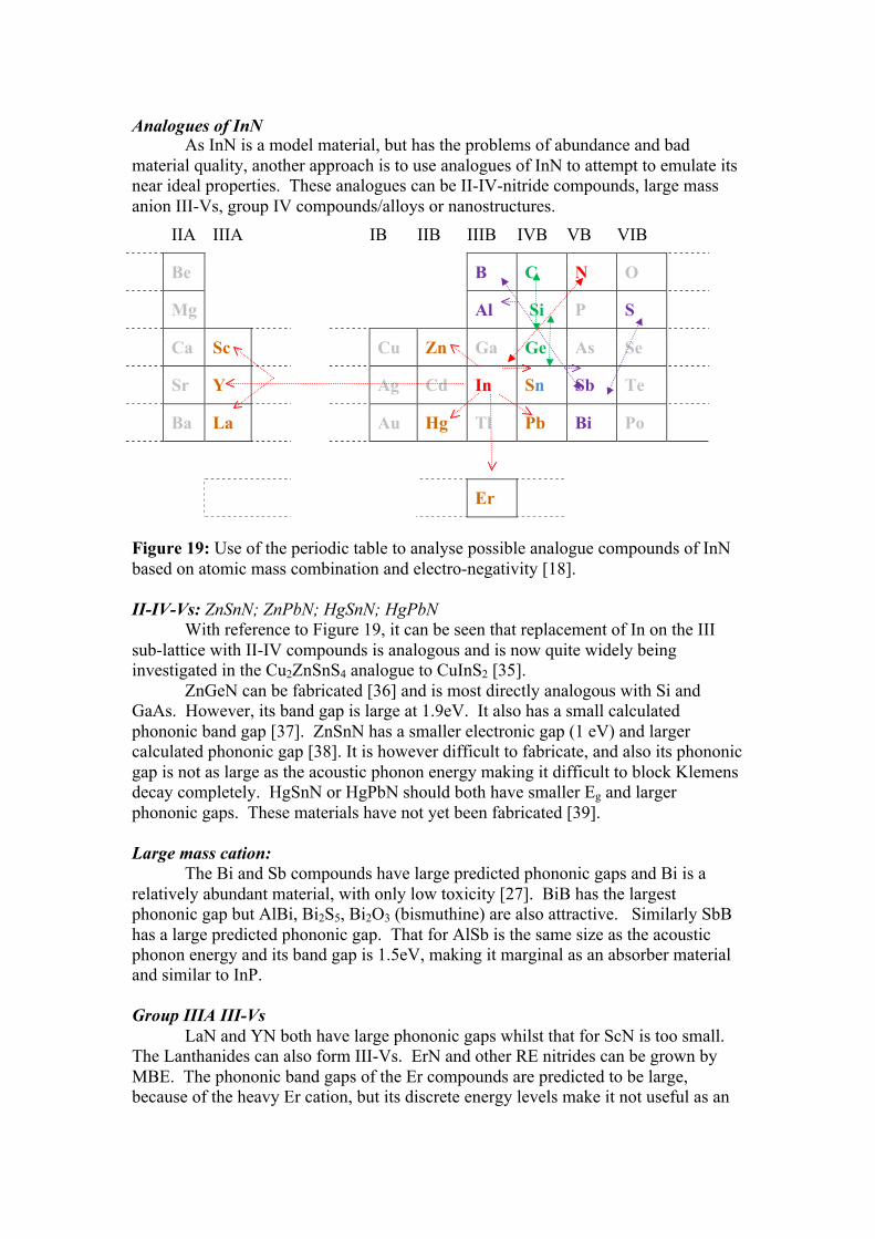
As InN is a model material, but has the problems of abundance and bad material quality, another approach is to use analogues of InN to attempt to emulate its near ideal properties. These analogues can be II-IV-nitride compounds, large mass anion III-Vs, group IV compounds/alloys or nanostructures. IIA IIIA IB IIB IIIB IVB VB VIB
Be B C N O
Mg Al Si P S
Ca Sc Cu Zn Ga Ge As Se
Sr Y Ag Cd In Sn Sb Te
Ba La Au Hg Tl Pb Bi Po
Er
Figure 19: Use of the periodic table to analyse possible analogue compounds of InN based on atomic mass combination and electro-negativity [18]. II-IV-Vs: ZnSnN; ZnPbN; HgSnN; HgPbN
With reference to Figure 19, it can be seen that replacement of In on the III sub-lattice with II-IV compounds is analogous and is now quite widely being investigated in the Cu2ZnSnS4 analogue to CuInS2 [35].
ZnGeN can be fabricated [36] and is most directly analogous with Si and GaAs. However, its band gap is large at 1.9eV. It also has a small calculated phononic band gap [37]. ZnSnN has a smaller electronic gap (1 eV) and larger calculated phononic gap [38]. It is however difficult to fabricate, and also its phononic gap is not as large as the acoustic phonon energy making it difficult to block Klemens decay completely. HgSnN or HgPbN should both have smaller Eg and larger phononic gaps. These materials have not yet been fabricated [39]. Large mass cation:
The Bi and Sb compounds have large predicted phononic gaps and Bi is a relatively abundant material, with only low toxicity [27]. BiB has the largest phononic gap but AlBi, Bi2S5, Bi2O3 (bismuthine) are also attractive. Similarly SbB has a large predicted phononic gap. That for AlSb is the same size as the acoustic phonon energy and its band gap is 1.5eV, making it marginal as an absorber material and similar to InP. Group IIIA III-Vs
LaN and YN both have large phononic gaps whilst that for ScN is too small. The Lanthanides can also form III-Vs. ErN and other RE nitrides can be grown by MBE. The phononic band gaps of the Er compounds are predicted to be large, because of the heavy Er cation, but its discrete energy levels make it not useful as an
absorber, although the combination of properties in a nanostructure could be advantageous. Group IV alloy/compounds:
All of the combinations Si/Sn, Ge/C or Sn/C look attractive with large gaps predicted in 1D models. However being all group IVs they only form weak compounds. Unfortunately SiC, whether 3C, 4H or 6H, has too narrow a phononic gap. Nonetheless GeC does form a compound and is of significant interest [40].
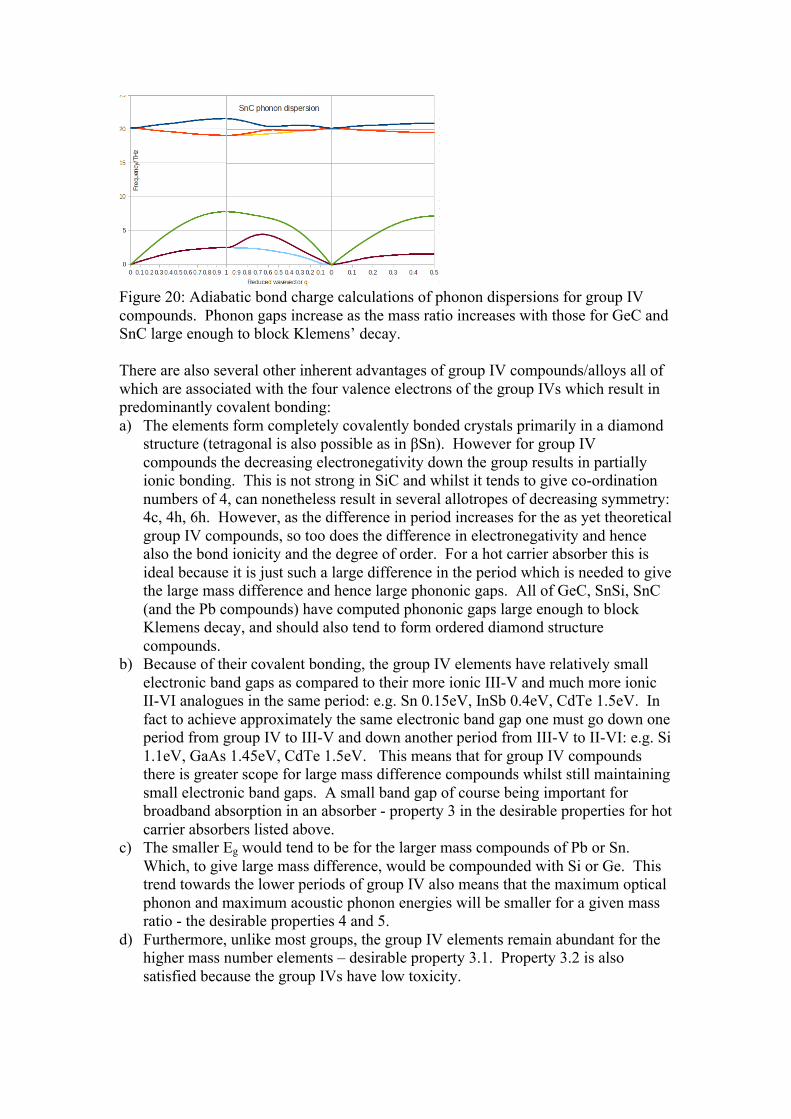
The calculated phonon dispersions for GeC, SnSi and SnC are shown in Figure 20 [41]. These are calculated using an adiabatic bond charge model. Force constants are input from bulk elemental values. There is not currently any allowance for Coulomb interactions and hence the splitting one would expect from polar effects in the optical phonons at zone centre is not present. However as these are largely covalent compounds this is not expected to be a big effect. Nonetheless it will be rectified in future work. The large gaps in the large mass ratios of GeC and SnC are larger than the respective acoustic phonon energies and hence should completely block Klemens’ decay. The narrow optical phonon dispersions (albeit slightly under-represented because of the lack of polarity mentioned above) should further limit secondary Ridley decay.
Figure 20: Adiabatic bond charge calculations of phonon dispersions for group IV compounds. Phonon gaps increase as the mass ratio increases with those for GeC and SnC large enough to block Klemens’ decay. There are also several other inherent advantages of group IV compounds/alloys all of which are associated with the four valence electrons of the group IVs which result in predominantly covalent bonding: a) The elements form completely covalently bonded crystals primarily in a diamond
structure (tetragonal is also possible as in βSn). However for group IV compounds the decreasing electronegativity down the group results in partially ionic bonding. This is not strong in SiC and whilst it tends to give co-ordination numbers of 4, can nonetheless result in several allotropes of decreasing symmetry: 4c, 4h, 6h. However, as the difference in period increases for the as yet theoretical group IV compounds, so too does the difference in electronegativity and hence also the bond ionicity and the degree of order. For a hot carrier absorber this is ideal because it is just such a large difference in the period which is needed to give the large mass difference and hence large phononic gaps. All of GeC, SnSi, SnC (and the Pb compounds) have computed phononic gaps large enough to block Klemens decay, and should also tend to form ordered diamond structure compounds.
b) Because of their covalent bonding, the group IV elements have relatively small electronic band gaps as compared to their more ionic III-V and much more ionic II-VI analogues in the same period: e.g. Sn 0.15eV, InSb 0.4eV, CdTe 1.5eV. In fact to achieve approximately the same electronic band gap one must go down one period from group IV to III-V and down another period from III-V to II-VI: e.g. Si 1.1eV, GaAs 1.45eV, CdTe 1.5eV. This means that for group IV compounds there is greater scope for large mass difference compounds whilst still maintaining small electronic band gaps. A small band gap of course being important for broadband absorption in an absorber - property 3 in the desirable properties for hot carrier absorbers listed above.
c) The smaller Eg would tend to be for the larger mass compounds of Pb or Sn. Which, to give large mass difference, would be compounded with Si or Ge. This trend towards the lower periods of group IV also means that the maximum optical phonon and maximum acoustic phonon energies will be smaller for a given mass ratio - the desirable properties 4 and 5.
d) Furthermore, unlike most groups, the group IV elements remain abundant for the higher mass number elements – desirable property 3.1. Property 3.2 is also satisfied because the group IVs have low toxicity.
Nanostructures: As discussed in the following section, QD nanostructures can be viewed in the same way as compounds. Their phononic properties can be estimated from consideration of their combination force constants. Hence it is possible to ‘engineer’ phononic properties in a wider range of nanostructure combinations. Of the materials discussed above the Group IVs lend themselves most readily to formation of nanostructures instead of compounds due to their predominantly covalent bonding, which allows variation in the coordination number. Therefore the nanostructure approaches below are consistent with a similar description as analogues of InN, whether it be III-V QDs, colloidally dispersed QDs or for core shell QDs.
Nanostructures for absorbers Nanostructures offer another possibility for replacement of InN as an absorber material. Nanostructures allow modification of the phonon dispersion of a composite material. III-V compounds or indeed most of the cubic and hexagonal compounds can be considered as very fine nanostructures consisting of ‘quantum dots’ of only one atom (say In) in a matrix (say N) with only one atom separating each ‘QD’ and arranged in two interpenetrating fcc lattices. Modelling of the 1D phonon dispersion in this way gives a close agreement with the phonon dispersion for zinc-blende InN extracted from real measured data for wurtzite material [20]. Similar ‘phonon band gaps’ should appear in good quality nanostructure superlattices, through coherent Bragg reflection of modes such that gaps in the superlattice dispersion open up [20]. There is a close analogy with photonic structures in which modulation of the refractive index in a periodic system opens up gaps of disallowed photon energies. Here modulation of the ease with which phonons are transmitted (the acoustic impedance) opens up gaps of disallowed phonon energies. Force constant modelling of III-V QD materials by SK growth 3D force constant modelling, using the reasonable assumption of simple harmonic motion of atoms in a matrix around their rest or lowest energy position, reveals such phononic gaps [42]. The model calculates longitudinal and transverse modes and can be used to calculate dispersions in a variety of symmetry directions and for different combinations of QD sub-lattice structure and super-lattice structure. III-V Stranski-Krastinov grown QD arrays of InAs in InGaAs and InGaAlAs matrices are fabricated by Professor Okada’s group at the University of Tokyo using MBE. We are investigating these for evidence of phonon dispersion modulation and potential slowed carrier cooling. In order to understand the expected phonon dispersions these are being modelled using the 3D force constant technique. Lattice matched and strain compensated material pairs that may produce large phonon band gaps are of interest. Previous iterations in the design of these structures indicated the importance of separating “light” and “heavy” atoms to different parts of the nanostructure. Initially, the lightest atom in the system, As, was present in both the QD and the matrix. This meant that the reduced mass of both regions (proportional to the sum of the inverses of each atomic mass) was very similar as the light element dominates in this case.
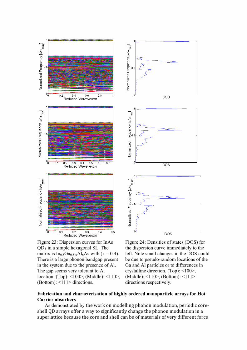
Figure 21: Schematic of the simple hexagonal superlattice of InAs QD disks, showing their relative dimensions. The red square indicates orthorhombic repeat unit for the simple hexagonal system. On this iteration structures with an In0.5Ga0.5-xAlxAs matrix (with x=0.4) and InAs QDs were grown. Significant Al content was introduced into these structures with the expectation that this light element, segregated to the matrix material, might produce appreciable phonon bandgaps. A schematic of the structure is shown in Figure 21. Some images derived from characterisation of the structures grown at the University of Tokyo are presented in Figure 22. The superlattice of QDs has a simple hexagonal structure. Extraordinary periodic out-of-plane stacking is achievable and largely defect free structures can be grown on the order of microns.
Figure 22: Some images of the InAs QD structure as grown using S-K MBE growth at the University of Tokyo. (Above): the near-perfect stacking of the structure is shown. (Above right): in-plane InAs QD arrangement. (Right): simple hexagonal superlattice structure showing stacking. The QDs are similar to flattened disks with in plane dimensions of 40-50 nm and heights of 7 nm.
Force constant modelling of this structure predicts an appreciable phonon band gap, as shown in Figures 23 & 24. This band gap is due almost entirely to the presence of the Al in the system. A small band gap is present due to the mass difference between In, Ga and As, but it is less than a quarter of the size shown in Figures 23 & 24. Due to computational constraints the size of the QDs is quite small, only about one nanometre in diameter. While actual sizes for these structures are too computationally intensive to model without extreme effort, recent modelling with gradually increasing size suggests that the dispersion relations scale linearly with size. That is, once the discrete distances (bond lengths) are small relative to the superlattice unit cell dimension, the dispersion should look exactly the same when scaled such that the relative dimensions are preserved. This will be investigated in greater detail in further work.
Figure 23: Dispersion curves for InAs QDs in a simple hexagonal SL. The matrix is In0.5Ga0.5-xAlxAs with (x = 0.4). There is a large phonon bandgap present in the system due to the presence of Al. The gap seems very tolerant to Al location. (Top): <100>, (Middle): <110>, (Bottom): <111> directions.
Figure 24: Densities of states (DOS) for the dispersion curve immediately to the left. Note small changes in the DOS could be due to pseudo-random locations of the Ga and Al particles or to differences in crystalline direction. (Top): <100>, (Middle): <110>, (Bottom): <111> directions respectively.
Fabrication and characterisation of highly ordered nanoparticle arrays for Hot Carrier absorbers As demonstrated by the work on modelling phonon modulation, periodic core-‐shell QD arrays offer a way to significantly change the phonon modulation in a superlattice because the core and shell can be of materials of very different force
constant, directly leading to a strong phonon confinement. Deposition methods are being investigated to fabricate such highly ordered QD arrays. The Langmuir-Blodgett (LB) technique fabricates thin films from colloidal dispersions of quantum dots (QDs). The LB technique allows for controllable, uniform film formation and subsequent transfer onto a solid substrate, such as quartz [43]. Through surface passivation of the QDs, interparticle spacing can also be controlled. Figure 25 illustrates the set-up of the LB apparatus and the functionalized QDs.
Figure 25: Langmuir-Blodgett set-up for film fabrication with surface functionalized Si NPs.
Initial work focused on fabrication of periodic thin films of Si nanoparticles (NPs) provided by the University of Minnesota. The Si NPs under investigation are surface passivated with dodecane (C12H26), a long chain hydrocarbon rendering the surface hydrophobic. The particles were dispersed in chloroform and investigated using TEM, UV-Vis spectroscopy and photoluminescence (PL). Using TEM imaging the average diameter was found to be 3.0±0.5 nm. Figure 26 (left) shows a droplet of solution (dispersed in chloroform) and the inset highlights the lattice fringes confirming the presence of silicon - a 3.14 Å lattice spacing corresponding to the {111} planes.
Figure 26: (Left) TEM images of Si NPs dried on a grid. (Right) TEM image of Si NPs monolayer deposited at 50 mN/m of SP. Monolayer structures of Si NPs have been successfully deposited using the LB method and characterisation has been on-going using TEM, UV-vis, PL and Raman spectroscopy. Figure 18 (right) illustrates TEM image of the Si films fabricated at 50 mN/m surface pressures (SP) of the water trough. As noted, high contrast is difficult to achieve due to the small density difference of Si and the carbon-passivating chains.
As a result, to further quantify the coverage and regularity, computer recognition software is required; on which work is on-going. Nonetheless, Figure 18 (right) appears to show a dense packing of Si NPs. UV-Vis spectroscopy was used to study the optical absorption of the films. As illustrated in Figure 27 (left) for single layers of Si NPs at varying compression surface pressures (SP), the absorption clearly increases when SP increases, corresponding to higher packing densities of Si NPs. The PL spectra of the above films show narrow and symmetric peaks at 1.6 ~1.7 eV, as shown in Figure 26 (right), which are in good agreement with the estimated band gap using the ‘effective mass approximation’. The red shift in emission energy from Si NPs films as compared to the solution corresponds to the electronic energy transfer from small particles to larger ones when they are closely packed [44] and to the overlap of wavefunction and mini-band formation with subsequent energy level broadening of the closely packed thin film.
Figure 27: (Left) Optical absorption of Si monolayers deposited at various surface pressures (SP). (Right) PL of Si NPs films at varying SP, as compared to the Si NPs solution. Investigation of the electronic and phononic properties of the monolayer and multilayer structures are on-going using low-wavenumber Raman and time resolved PL spectroscopy. Implementation of nanostructures for Hot Carrier cells In order to use a nanoparticle array as a Hot Carrier absorber, and hence utilise slowed carrier cooling due to modified phonon dispersion, then a way to fabricate a complete structure with ESCs must be established. The multiple nano-well structures have demonstrated reduced carrier cooling by enhancing the phonon bottleneck, probably at a stage prior to optical phonon decay. Large phononic band gap materials have strong potential to block Klemens decay of optical phonons. A structure combining both structures should give even greater reduction in carrier cooling rates as the mechanisms should not interfere directly with each other and hence their effects should be additive [18]. A combined absorber for a hot carrier cell should look similar to Figure 28.
0.5 1.5 2.5 3.5 4.5Energy (eV)
absorptio
n (a.u)
40mN/m
60mN/m
65mN/m
collapse
Figure 28: Hot Carrier cell design combining Multiple Nano-Well with phononic band gap materials: (a) schematic and (b) band structure for InN/InGaN epitaxial multiple nanowell with phononic band nano-wells; (c) band structure with nano-wells of analogues of InN with large phononic band gap with thin film barriers [18]. This has narrow nano-wells of large phononic band gap material, not necessarily thin enough to give quantum confinement, separated by thin barriers. The barriers would either have an electronic band offset to block hot carrier diffusion or an optical phonon energy offset with the nano-wells and probably a coherent nano-well structure, or all three, depending which of the multiple nano-well (MNW) mechanisms, discussed above, is dominant. This will enhance the phonon bottleneck either by preventing hot carrier diffusion, by reflecting and confining optical phonons or by blocking certain folded phonon modes, respectively, or all three. The phononic band gap nano-wells themselves will further enhance phonon bottleneck by preventing Klemens decay of optical to acoustic phonons. This should maximise the phonon bottleneck and minimise carrier cooling for a given illumination intensity. A lattice matched pair of large phononic band gap nano-well and barrier materials (InN/InGaN) is suggested in Figure 28 (b), whereas in (c) a wider range of possible InN analogue phononic band gap materials could be used in a thin film structure with thin probably oxide barriers. The thin barriers (a few nm) should facilitate tunnelling between wells and hence transport of the carriers to the contacts. The contacts are energy selective for the front contact with a double barrier resonant tunnelling structure. In Figure 28 (b) this will be lattice matched to the absorber, probably a InGaN/InN/InGaN with the In QW thin enough to give widely spaced confined energy levels. Probably both an electron ESC on the front surface and a hole ESC contact on the back surface will be used for this high quality proof of concept. For Figure 28 (c), thin film contacts will be used with a double oxide barrier with Si QW or QD resonant tunnelling structure with widely spaced confined levels. For this device only the front electron contact will be an ESC, the rear contact will be a simple large work function hole contact, possibly with an electron blocking semiconductor. Hence Figure 28 (b) represents a high quality epitaxial structure suitable to demonstrate the hot carrier cell with the potential for high efficiencies, whereas
a) b)
c)
Figure 28 (c) a thin film structure with both much more readily abundant materials and much simpler thin film fabrication particularly with respect to the single ESC. Summary of work on Hot Carrier solar cells The project has seen significant development in all areas of the Hot Carrier solar cell work on the project. The modeling of efficiencies not only now includes real material parameters for highly promising absorber materials such as InN, but also is now extended to Energy Selective contacts of finite width. The transport across such contacts is further modeled for a range of QD matrix combinations. Collaboration with the IRDEP node on this topic has shown that the difference between models of the relative importance placed on hot carrier Auger effects makes a difference to the influence of contact width on efficiency - with a high probability of Auger effects requiring narrower contact width to give high efficiency whereas this sensitivity is much weaker for low probability Auger. Work on ESCs has seen demonstration of the necessary resonance in Si QD/SiO2 double barrier resonant tunneling structures, albeit very small as yet. In strong collaboration with the USyd node, measurement of carrier cooling rates in InN with time-resolved PL has indicated evidence for slowed carrier cooling, which is corroborated in the literature, further demonstrating the importance of a large phonon band gap to block optical phonon decay, but also highlighting the importance of material quality. Comparison of the InP/GaAs phononic/non-phononic band gap semiconductor pair indicates the much slower carrier cooling in a phononic band gap material. The observed effects of slowed carrier cooling in several MQW systems in literature have been described in terms of three potential models for enhancement of phonon bottleneck effects. This work in collaboration with the IRDEP node, is now developing into experiments to determine the dominant mechanisms. Phononic band gaps for reduced optical phonon decay have been investigated further with both the III-nitride system identified as a good model material and the identification of a range of InN analogue materials of more abundant elements and greater ease of fabrication. Modeling of nanostructurs for absorber materials has focused on real III-V QD structures, showing phonon band gaps which will soon be measured in phonon dispersion measurements. Progress on the Langmuir-Blodgett approach to ordered nanoparticle arrays has seen development of ordered single layer arrays of Si nanoparticles. The potential application of nanostructures to fully integrated devices has been investigated conceptually, with various designs considered which include the demonstrated slowed cooling effects of QWs, the phonon decay blocking effects of phononic band gap materials and the integration of energy selective contacts. Specific designs are being developed which can a) prove the concept of hot carrier cells through use of high quality epitaxialy grown material, and b) use abundant materials in thin film growth modes to demonstrate the feasibility of large scale fabrication. Further Work Modeling work on efficiencies, energy selective contacts and phononic properties will be continued. Measurements on test structures for phonic properties will be extended to other materials. These will include time resolved PL for carrier cooling
and high resolution Raman for phonon density of states. New nanostructures will be investigated, including III-V quantum well and quantum dot nanostructures with collaborators. These will build on the very promising results obtained for reduced carrier cooling measured in these nanostructures with the USyd node. Further work on colloidal nanostructures will investigate multi-layer uniform quantum dot arrays, and investigate their optical and electrical properties. Using both Si QD arrays and other core shell QD structures. Further work on energy selective contact materials will be carried out in which the quality of materials is improved, the quality of barriers and size uniformity of QDs, as well as double and triple barrier QW structures. Building on the initial work on complete devices, complete device structures incorporating both absorber and energy selective contacts will be fabricated, by collaborators and in-house, and measured for carrier cooling and electrical I-V properties, with the aim of demonstrating a true Hot Carrier cell effect. Publications on the project Refereed Journal papers: 1. Y. Feng, P. Aliberti, B.P. Veettil, R. Patterson, S. Shrestha, M.A. Green, G. Conibeer, Non-ideal
energy selective contacts and their effect on the performance of a hot carrier solar cell with an indium nitride absorber, Applied Physics Letters, 100, 053502 (2012).
2. Binesh Puthen Veettil, Dirk König, Robert Patterson, Gavin Conibeer and Martin A. Green, “Optimized multilayer double barrier resonant tunnelling structures with high conductivity and energy selectivity”, EuroPhysics Letters, 96(5) (2011) 57006. DOI: http://dx.doi.org/10.1209/0295-5075/96/57006 (2011)
3. P. Aliberti, Y. Feng, S.K. Shrestha, M.A. Green, G. Conibeer, Li-Wei Tu , Po-Han Tseng , R. Clady, Applied Physics Letters, 99(22) (2011) 223507, Effects of non-ideal energy selective contacts and experimental carrier cooling rate on the performance of an indium nitride based hot carrier solar cell, Applied Physics Letters, accepted Nov 2011.
4. P. Aliberti, Y. Feng, Y. Takeda, S. K. Shrestha, M. A. Green, G. Conibeer, Investigation of theoretical efficiency limit of hot carriers solar cells with a bulk indium nitride absorber, Journal of Applied Physics, 108 (2010) 094507.
5. R. Patterson, M. Kirkengen, B. Puthen Veettil, D. Konig, M.A. Green, G. Conibeer, Phonon lifetimes in model quantum dot superlattice systems with applications to the hot carrier solar cell, Solar Energy Materials and Solar Cells, 94 (Nov 2010) 1931-1935.
6. R. Clady, M.J.Y. Tayebjee, P. Aliberti, D. Konig, N.J. Ekins-Daukes, G.J. Conibeer, T.W. Schmidt, M.A. Green, Interplay between Hot phonon effect and Intervalley scattering on the cooling rate of hot carriers in GaAs and InP, Progress in Photovoltaics, accepted March 2011.
7. Y. Takeda, T. Motohiro , D. König , P. Aliberti, Y. Feng , S. Shrestha , G. Conibeer, Practical factors lowering conversion efficiency of hot carrier solar cells, Applied Physics Express, Applied Physics Express 3 (2010) 104301.
8. P. Aliberti, S.K. Shrestha, R. Teuscher, B. Zhang, M.A. Green, G.J. Conibeer, Study of Silicon Quantum Dots in a SiO2 Matrix for Energy Selective Contacts Applications, Solar Energy Materials and Solar Cells, 94 (2010)1936-1941.
9. C. Flynn, D.Konig, M.A.Green, G.Conibeer, Modelling of metal–insulator–semiconductor devices featuring a silicon quantum well, Physica E, 42 (2010) 2211-2217. doi:10.1016/j.physe.2010.04.019.
10. C Flynn, D König, I Perez-Wurfl, M A Green, G Conibeer, “Correlation between fixed charge and capacitance peaks in silicon nanocrystal metal–insulator–semiconductor devices”, Semiconductor Science and Technology,. 25 (2010) 045011 (8pp).
11. G Conibeer, R Patterson, L Huang, J-F Guillemoles, D Konig, S Shrestha, MA Green, “Modelling of hot carrier solar cell absorbers”, Solar Energy Materials and Solar Cells, 94 (2010) 1516-1521. doi:10.1016/j.solmat.2010.01.018.
12. Santosh K. Shrestha, Pasquale Aliberti, Gavin J. Conibeer, Energy selective contacts for hot carrier solar cells, Solar Energy Materials and Solar Cells, 94 (Sept 2010) 1546-1550.
13. D. König, K. Casalenuovo, Y. Takeda, G. Conibeer, J.F. Guillemoles, R. Patterson, L.M. Huang, M.A. Green, “Hot Carrier Solar Cells: Principles, Design and Materials”, Physica E: Low-dimensional Systems and Nanostructures, 42 (2010) 2862-2866.
14. G.J. Conibeer, N. Ekins-Daukes, D. König, E-C. Cho, C-W. Jiang, S. Shrestha, M.A. Green, Solar Energy Materials and Solar Cells, 93 (2009) 713-719, “Progress on Hot Carrier solar cells”.
15. Y. Takeda, T. Ito, T. Motohiro, D. König, S. Shrestha, G. Conibeer, Journal of Applied Physics, 105, (2009) 074905, "Hot carrier solar cells operating under practical conditions".
16. Y. Takeda, T. Ito, R. Suzuki, T. Motohiro, S. Shrestha, G. Conibeer, “Impact ionization and Auger recombination at high carrier temperature”, Solar Energy Materials & Solar Cells, 93 (June 2009) 797-802.
17. G.J. Conibeer, D. König, M.A. Green , J.F. Guillemoles, “Slowing of carrier cooling in Hot Carrier solar cells”, Thin Solid Films, 516 (July 2008) 6948.
18. G. Conibeer, C.-W. Jiang, D. König, S. Shrestha, T. Walsh, M.A. Green “Selective energy contacts for hot carrier solar cells”, Thin Solid Films, 516 (July 2008) 6968.
Refereed Conference papers: 1. G. Conibeer, Proc. SPIE Photonic West (Jan 2012), “Hot Carrier cells: an example of Third
Generation Photovoltaics”. 2. S. Lee, R. Lin, S. Huang, G. Conibeer, M.A. Green, “Structural and optical properties of doped Ge
nanostructures with Si3N4 barrier fabricated by rf-magnetron sputtering”, Proc. 49th AuSES conference Solar2011, refereed paper (Sydney, Nov 2011).
3. S. Lee, S. Huang, G. Conibeer, M.A. Green, Structural and Optical Study of Ge nanocrystals Embedded in Si3N4 Matrix, Energy Procedia, (10, Nov 2011), 271-281, Special issue for the IU-MRS, Symposium R, Nice May 2011.
4. P. Aliberti, B. Zhang, M.A. Green. G. Conibeer, S. Shrestha, A. Hsieh, R. Li, B. Puthen-Veettil, Australian Solar Energy Society conference, Solar2010 (Canberra Dec 2010), “Investigation of single layers of silicon quantum dots in SiO2 matrix for energy selective contacts in hot carriers solar cells”, December 2010.
5. G. Conibeer, Australian Solar Energy Society conference, Solar2010 (Canberra Dec 2010), “Third Generation Photovoltaics”, December 2010.
6. A. Hsieh, S. Shrestha, M.A. Green. G. Conibeer, Australian Solar Energy Society conference, Solar2010 (Canberra Dec 2010), “Investigation of Si/SiO2 quantum well structures for selective energy contacts in hot carrier solar cells”, December 2010.
7. F. QI, G. Conibeer, S. Shrestha, S. Huang, Australian Solar Energy Society conference, Solar2010 (Canberra Dec 2010), “The study of potential application of Group IV alloys in photovoltaic field”, December 2010.
8. B. Puthen-Veettill, D. König, M.A. Green, G. Conibeer, Energy Procedia, 2(1) (2010), p. 213-219, “Impact of disorder in double barrier QD structures on energy selectivity investigated by a 2-Dimensional model”, Proc. E-MRS Spring meeting, Symposium B, June 2009, 10.1016/j.egypro.2010.07.031 http://www.elsevier.com/wps/find/journaldescription.cws_home/718157/description#description
9. G. Conibeer, “Third generation photovoltiacs”, (invited), Proceedings of SPIE – Optics and Photonics – Next Generation (Nano) Photonic & Cell Technologies for Solar Energy Conversion, San Diego, August 2009, Proc. SPIE, Vol. 7411 (2009) 741103??; doi:10.1117/12.825583??.
10. G. Conibeer, IEEE proceedings of ETSC conference, London Sept 08, invited plenary paper, “Third Generation Photovoltaics”, pp 45-50.
11. Santosh K Shrestha, Pasquale Aliberti, Gavin J Conibeer, “Investigation of Energy Selective Contacts for Hot Carrier Solar Cell”, Proc. Int. Solar Energy Society, Asia Pacific region, Conf. (Sydney 2008).
12. R. Patterson, M. Kirkengen, A. Hsieh, M.A. Green, G. Conibeer, “Modelling of QD superlattices for Hot Carrier cell absorbers”, Proc. Int. Solar Energy Society, Asia Pacific region, Conf. (Sydney 2008).
13. B. Puthen-Veettil, Dirk König, M. A. Green, G. Conibeer, “2-Dimensional model of the resonant tunnelling through an ideal double barrier structure.”, Proc. Int. Solar Energy Society, Asia Pacific region, Conf. (Sydney 2008).
Un-refereed Conference papers:
1. G. Conibeer, R. Patterson, P. Aliberti, H. Xia, S. Huang, D. König, B. Puthen-Veettil, S. Shrestha, M.A. Green, “Hot Carrier solar cells: Choice of Materials for Efficiency and Abundance”, 26th European Photovoltaic Solar Energy Conference, Hamburg, Germany, September 2011.
2. B. Puthen Veettil, D. König, R. Patterson, M.A. Green, G. Conibeer, “Electronic states and tunnelling transport in an array of quantum dots with arbitrary shapes”, 26th European Photovoltaic Solar Energy Conference, Hamburg, Germany, September 2011.
3. D. König, Y. Takeda, B. Puthen-Veettil, G. Conibeer, “Lattice-Matched Hot Carrier Solar Cell with Energy Selectivity Integrated Into Hot Carrier Absorber”, PVSC, Fukuoka, Nov 2011.
4. M. A. Green, G. Conibeer, D. König, S. Shrestha, S. Huang, P. Aliberti, L. Treiber, R. Patterson, B. Puthen Veettil, A. Hsieh, A. Luque, A. Marti, P.G. Linares, E. Cánovas, E. Antolín, D. Fuertes Marrón, C. Tablero, E. Hernández, J-F. Guillemoles , L. Huang, T. Schmidt, R. Clady and M. Tayebjee, “Recent Progress with Hot Carrier Solar Cells”, 25th European Photovoltaic Solar Energy Conference and Exhibition (25th EU PVSEC) / 5th World Conference on Photovoltaic Energy Conversion (WCPEC-5), Session: 1AP.1.1, Abstract No. [1191], Valencia, Spain, 6-10 September, 2010 (plenary).
5. P. Aliberti, Y. Feng, R.Clady, M.J.Y. Tayebjee, T.W. Schmidt, S.K. Shrestha, M.A. Green, G.J. Conibeer, “On efficiency of hot carriers solar cells with a Indium nitride absorber layer”, Oral Presentation, Proceedings of European photovoltaic conference, Valencia, Spain, 6-10 September 2010.
6. A. Hsieh, S. Shrestha, M.A. Green, G. Conibeer, ‘Investigation of Si/SiO2 quantum well structures for energy selective contacts in hot carrier solar cells’, 5th World Photovoltaic Solar Energy Conference, Valencia, Spain, 6-10 September 2010.
7. R. Patterson, B. Puthen Veettil, M. Kirkengen, D.Koenig, M.A. Green, G.J. Conibeer, Poster Presentation 1DV.3.77, 5th World PVSEC, Valencia, Spain, 6 - 10 September, 2010.
8. B. Puthen Veettil, R. Patterson, D. König, G. Conibeer and M. A. Green, “Modelling the Effects of Doping in Quantum Dot Structures for Tandem Cells”, Poster Presentation 1DV.3.64, 5th World PVSEC, Valencia, Spain, 6 - 10 September 2010.
9. M.A. Green, G. Conibeer, D. König, S. Shrestha, S. Huang, P. Aliberti, L. Treiber, R. Patterson, B. Puthen-Veettil, A. Hsieh, Y. Feng, A. Luque, A. Marti, P.G. Linares, E. Cánovas, E. Antolin, D. Fuertes Marrón, C. Tablero, E.Hernandez, J-F. Guillemoles, L. Huang, A. Le Bris, T. Schmidt, R. Clady and M. Tayebjee, “Hot Carrier Solar Cells: Challenges and Recent Progress”, 35th IEEE Photovoltaic Specialists Conference, Honolulu, Hawaii, 20-25 June, 2010.
10. R. Patterson, Z. Wan, B. Puthen-Veettil, D. König, G. Conibeer, “Phonon Decay in Naostructure: Computational Study”, Proc. of 35th IEEE PVSC, Honolulu, Hawaii, 20 - 25 June 2010, proc. pp. 1843 (art.-no. 5615953).
11. G. Conibeer, R. Patterson, P. Aliberti, L. Huang, J.-F. Guillemoles, D. König, S. Shrestha, R. Clady, M. Tayebjee, T. Schmidt and M.A. Green, “Hot Carrier Solar Cell Absorbers”, 24th European Photovoltaic Solar Energy Conference, Hamburg, Germany, 21-25 September 2009.
12. R. Patterson, M. Kirkengen, B. Puthen-Veettil, D. König, M.A. Green and G. Conibeer, "Phonon lifetimes in model quantum dot superlattices", 24th European Photovoltaic Solar Energy Conference, Hamburg, Germany, 21-25 September 2009.
13. B. Puthen Veettil, D. König, G. Conibeer and M. A. Green, “Theoretical Analysis of Energy Selective Contacts with Si QDs in SiO2 Matrix with SiC Barriers Using a 2 Dimensional Model”, 24th European Photovoltaic Solar Energy Conference, Hamburg, Germany, 21-25 September 2009.
14. A. Hsieh, S. Shrestha, M.A. Green, G. Conibeer “Investigation of Si/SiO2 multilayer structures with 2nm Si sublayer thickness by reactive magnetron sputtering for selective energy contacts”, 19th International Photovoltaic Science and Engineering Conference & Exhibition, Jeju, South Korea, 9-13 November 2009 (Oral presentation).
15. G. Conibeer, R. Patterson, L. Huang, J-F. Guillemoles, D. Kőnig, S. Shrestha, MA. Green, “Modelling of Hot Carrier Solar Cell Absorbers”, Technical Digest of 18th International Photovoltaic Science and Engineering Conference (PVSEC-18), Kolkata, India, 19-23 January 2009.
16. S. Shestha, P. Aliberti, G. Conibeer, “Energy Selective Contacts for Hot Carrier Solar Cells”, Technical Digest of 18th International Photovoltaic Science and Engineering Conference (PVSEC-18), Kolkata, India, 19-23 January 2009.
17. G.J. Conibeer, R. Patterson, L. Huang, J-F. Guillemoles, D. König, S. Shrestha, M.A. Green, “Hot Carrier Solar Cell Absorbers”, Proc 23rd European PV SEC (Valencia, Sept. 2008) 156.
18. L. Treiber, C. Bumby, S. Huang, G. Conibeer, “Preparation of Silicon Nanoparticles from Colloidal Dispersions for Monolayer Formation Using Langmuir-Blodgett Technique”, Proc. 23rd European Photovoltaic Solar Energy Conference, Valencia, Spain (2008) 624.
Contacts Emails of the PIs are: Gavin Conibeer: [email protected] Martin A Green: [email protected] References 1. G.J. Conibeer, C-W. Jiang, D. König, S. Shrestha, T. Walsh, M.A. Green “Selective energy contacts for hot carrier solar cells”, Thin Solid Films, 516 (July 2008) 6968.
2. M. A. Green, “Third Generation Photovoltaics: Ultra-High Efficiency at Low Cost” (Springer- Verlag, 2003). 3. P. Würfel, “Solar Energy Conversion with Hot Electrons from Impact Ionisation”, Sol. Energy
Mats. and Sol. Cells. 46 (1997) 43. 4. Ross R and Nozik AJ, J. Appl Phys, 53 (1982) 3318. 5. V.Y. Davydov, et al., “Absorption and emission of hexagonal InN: Evidence of narrow
fundamental band gap”, Physica Status Solidi (B), 229 (2002) p. r1-r3. 6. D. Fritsch, H. Schmidt, M. Grundmann, “Band dispersion relations of zinc-blende and wurtzite
InN”, Physical Review B, 69 (2004) 165204. 7. Y. Takeda, T. Ito, T. Motohiro, D. König, S.K. Shrestha, G. Conibeer, “Hot carrier solar cells
operating under practical conditions”, Journal of Applied Physics, 105 (2009) 074905-10. 8. P. Wurfel, A.S. Brown, T.E. Humphrey, and M.A. Green, Particle conservation in the hot-carrier
solar cell”, Progress in Photovoltaics, 13 (2005) 277-285. 9. P. Aliberti, Y. Feng, Y. Takeda, S.K. Shrestha, M.A. Green, G.J. Conibeer, “Investigation of
theoretical efficiency limit of hot carrier solar cells with bulk InN absorber”, Journal of Applied Physics, 108 (2010) 094507-10.
10. G. Conibeer, C.W. Jiang, D. König, S.K. Shrestha, T. Walsh, M.A. Green, “Selective energy contacts for hot carrier solar cells”, Thin Solid Films, 216 (2008) 6968-6973.
11. Y. Y. Feng, P. Aliberti, B.P. Veettil, R. Patterson, S. Shrestha, M.A. Green, G. Conibeer, Non-ideal energy selective contacts and their effect on the performance of a hot carrier solar cell with an indium nitride absorber, Applied Physics Letters, 100, 053502 (2012).
12. M. Zacharias, J. Heitmann, R. Scholz, U. Kahler, M. Schmidt, Appl. Phys. Lett. 80(2002) 661. 13. U. Kahler, Hofmeister, Optical Materials, 17 (2001) 83. 14. H. Takagi, H. Ogawa, Y. Yamazaki, A. Ishizaki, T. Nakagiri, Appl. Phys. Lett. 56, 2379 (1990). 15. S. Takeoka, M. Fujii and S. Hayashi, Phys. Rev. B 62, 16820 (2000). 16. G. Conibeer, M. Green, E-C. Cho, D. König, Y-H. Cho, T. Fangsuwannarak, G. Scardera, E. Pink,
Y. Huang, T. Puzzer, S. Huang, D. Song, C. Flynn, S. Park, X. Hao, D. Mansfield, “Silicon quantum dot nanostructures for tandem photovoltaic cells”, Thin Solid Films, 516 (July 2008) 6748.
17. Lopez et al., Appl. Phys. Lett. 80 (2002) 1637. 18. G. Conibeer, Proc. SPIE Photonic West (Jan 2012), “Hot Carrier cells: an example of Third
Generation Photovoltaics”. 19. D. König, K. Casalenuovo, Y. Takeda, G. Conibeer, J.F. Guillemoles, R. Patterson, L.M. Huang,
M.A. Green, “Hot Carrier Solar Cells: Principles, Materials and Design”, Physica E, 42 (2010) 2862-2866.
20. G. Conibeer, N.J. Ekins-Daukes, J-F. Guillemoles, D. König, E-C. Cho, C-W. Jiang, S. Shrestha and M.A. Green, “Progress on Hot Carrier Cells”, Solar Energy Materials and Solar Cells, 2009, 93, 713.
21. Rosenwaks, Y., Hanna, M. Levi, D., Szmyd, D., Ahrenkiel, R. and Nozik, A., “Hot-carrier cooling in GaAs: quantum wells versus bulk,” Phys Rev B, 48, 14675-14678 (1993).
22. Guillemoles, J-F, Conibeer, G. and Green, M.A., “On achievable efficiencies of Hot Carrier Solar
cell absorbers based on reported experimental thermalisation properties,” Proc. 21st European Photovoltaic Solar Energy Conference, Dresden Germany, 234–237 (2006).
23. Hirst, L., Führer, m., LeBris, A., Guillemoles, J-F., Tayebjee, M., Clady, R., Schmidt, T., Wang, Y., Sugiyama, M. and Ekins-Daukes, “,” Proc. 37th IEEE PV Specialists Conference, Seattle, talk 927 (2011).
24. Colvard, C., Gant, T.A. and Klein, M.V., “Folded acoustic and quantized optic phonons in (GaAl)As superlattices,” Physical Review B, 31, 2080-2091 (1985).
25. Zebarjadi, M., Bian, Z., Singh, R., Shakouri, A., Wortman, R., Rawat, V and Sands, T., “Thermoelectric Transport in a ZrN/ScN Superlattice,” Journal of Electronic Materials, Vol. 38(7), 960-6963 (2009).
26. Lee, S-M., Cahill, D.G. and Venkatasubramanian, R., “Thermal conductivity of Si–Ge superlattices”, Appl Phys Lett 70, 2957-2959 (1997).
27. Conibeer, G.J., König, D., Green, M.A. and Guillemoles, J.F., “Slowing of carrier cooling in Hot Carrier solar cells”, Thin Solid Films, 516, 6948-6952 (2008).
28. P.G. Klemens, Phys. Rev. 148 (1966) 845. 29. G. Conibeer, R. Patterson, P. Aliberti, L. Huang, J-F. Guillemoles, D. König, S. Shrestha, R.
Clady, M. Tayebjee, T. Schmidt, M.A. Green “Hot Carrier solar cell Absorbers”, 24th European PVSEC, Hamburg (Sept. 2009).
30. H. Bilz, W. Kress, “Phonon dispersion relations in Insulators”, Springer-Verlag (1979). 31. Y.C. Wen, Y.C., C.Y. Chen, C.H. Shen, S. Gwo, C.K. Sun, “Ultrafast carrier thermalization in
InN”, Applied Physics Letters, 89 (2006) 3; M.D. Yang, et al., “Hot carrier photoluminescence in InN epilayers”, Applied Physics A - Materials Science & Processing, 90 (2008) 123-127.
32. K.T. Tsen, J.G. Kiang, D.K. Ferry, H. Lu, W.J. Schaff, H.W. Lin, S. Gwo, “Direct measurements of the lifetimes of longitudinal optical phonon modes and their dynamics in InN”, Applied Physics Letters, 90 (2007) 3.
33. F. Chen, A.N. Cartwright, H. Lu, W.J. Schaff, “Ultrafast carrier dynamics in InN epilayers”, Journal of Crystal Growth, 269 (2004) 10-14.
34. R. Clady, M.J.Y. Tayebjee, P. Aliberti, D. Konig, N.J. Ekins-Daukes, G.J. Conibeer, T.W. Schmidt, M.A. Green, “Interplay between Hot phonon effect and Intervalley scattering on the cooling rate of hot carriers in GaAs and InP”, Progress in Photovoltaics, accepted March 2011.
Shrestha, S. and Green, M.A., “Hot Carrier cell absorber materials,” Proc. 26th European Photovoltaic Solar Energy Conference Hamburg, (2011).
42. R. Patterson, M. Kirkengen, B. Puthen Veettil, D. Konig, M.A. Green, G. Conibeer, Sol. Ener. Mats. And Sol. Cells, 94 (2010) 1931-1935.
43. S. Huang, K. Minami, H. Sakaue, S. Shingubara, T. Takahagi, “Effects of the surface pressure on the formation of Langmuir-Blodgett monolayer of nanoparticles”, Langmuir, 20 (2004), 2274.
44. C. R. Kagan, C. B. Murray, M. Nirmal, M. G. Bawendi, Phys. Rev. Lett. “Electronic Energy Transfer in CdSe Quantum Dot Solids”, 76 (1996) 1517.
Project: “Hot Carrier solar cell: Implementation of the Ultimate PV Converter” Institution (node): IRDEP, Paris, France Final Report April 2012 Investigators Note: all investigators are member of IRDEP but not necessary under contract with CNRS, in which case they are not supported by the grant. Jean-François Guillemoles, Research director, CNRS, PI Daniel Lincot, Research director, CNRS Laurent Lombez, Researcher, CNRS Par Olsson, EDF research engineer Sana Laribi, EDF research engineer Christophe Domain, EDF research engineer Marie Jubault, research engineer, CNRS Arthur LeBris, Graduate researcher, CNRS Hugo Levard, Graduate researcher, CNRS Hanane El Begheti, Graduate researcher, CNRS Myriam Paire, Graduate researcher, CNRS Artabaze Shams, Graduate researcher, CNRS Jean Rodière, Graduate researcher, CNRS Florian Proise, Graduate researcher, CNRS Christian Andriamiadamanana, Graduate researcher, CNRS Abstract
Tapping into the thermal energy losses incurred during photovoltaic conversion and bringing solar cells closer to their limiting efficiency helps bringing solar photovoltaics closer to large scale use. This is the reason behind the proposition to study Hot carrier solar cells, also dubbed "the ultimate solar cell", because they are the simplest scheme that enables, in principle, to achieve limiting thermodynamic efficiencies (86% under maximal solar concentration.
This project aimed at demonstrating experimentally such a device, while attempting to elaborate one using non-toxic and sustainable processes, i.e. compatible with a large scale application.
At the starting date of the project, hot carriers solar cells were hardly more than a concept, but already, several challenges had been identified: (i) obtaining a slow enough thermalization of carriers in the absorber and (ii) efficiently extracting those carriers to obtain an increased output voltage.
We have worked on the extraction and collection of hot carriers and obtained an important by modeling the thermalization in the contacts : the contact selectivity may
not be as drastic as initially thought, and that semi-selective contacts only should be enough to obtain most of the hot carrier effect.
On the experimental side, and in collaboration with IES, we have designed III-V heterostructures based on antimonides to extract thermalization rates from Photoluminescence experiments. These were found compatible with conversion efficiencies at maximal (x 46200) solar concentration above 40%.
Based on the previous findings, we have been able recently to make III-Sb heterostructures (in collaboration with IES) and to characterize them. Best thermalization rates obtained were ~80 W/K/cm² , at room temperature, but under large illumination fluxes (equivalent to ~x 50 000 suns). When these were tested as devices, Voc > 400 mV were obtained under moderate concentration (~x 400) , that is 200 mV only below the band gap of the absorber, which compares favorably with state of the art GaSb solar cells. Efficient carrier extraction over the collection barrier was also demonstrated at short circuit . Further analysis of the device are under way.
Reducing the solar concentration for the operation of the device would require an equivalent reduction of the thermalization rates. This has been attacked on fronts : (i) modeling showed that reducing the thickness of the absorber while maintaining its absorptivity would result is a proportional reduction of the thermalisation rates and (ii) ab initio design of nanostructured materials with a reduced thermalisation rate. Case (i) was studied in the context of the advances in nanophotonics and especially those made at our partnering institutions, LPN and LCFIO. Case (ii) involved the ab initio modeling of Si-Ge based nanostructures, some of which displayed a reduced thermalisation as compared to bulk Si. Introduction
The original plan consisted, in short, to contribute to the making of a new, very
efficient, type of solar cell: the hot carrier device. Ideally this device should also be made from non-toxic and earth abundant materials (e.g. Si). See Overview introduction. Background See Overview.
Figure 1: Schematic band diagram of a hot carrier solar cell. Results
Important progress has been made towards the realisation of the objectives, albeit, realisation of device based on Silicon seems still difficult, meanwhile a structure and technologically well mastered materials (III-V) have emerged that could form a proof of concept.
On the basic science side, hot carrier solar cell operation is now rather well understood. Models have been developed that enable to describe realistic devices, either based on detailed balance, or using the more sophisticated Ensemble Monte Carlo (EMC) method. Notably:
- Development of a simulation package that predicts the device efficiency as a function of selected material parameters (carrier lifetimes, thermalisation rate constant, band alignment, absorption coefficient,…)
- Definition of a scheme for carrier extraction: initially it was though that the
device would need very selective contacts. We proposed a structure based on semi-selective contacts, much simpler to realise in practice (it is simply a barrier of a well adjusted height) that would yield most of the efficiency gain of a fully selective contact (APL 2010). This is a very significant contribution towards the making of these devices.
- Utilisation of an EMC code (developed at IEF, [Tea 2011]) to validate the
assumption made for the detailed balance model : indeed the carrier distribution was found Fermi-Dirac like in an InGaAs model system, even in the very high injection regime. It was found that carrier extraction, even via an energy selective
contact, would not alter this finding, and that carrier extraction was not limiting the current.
On the experimental side, we have made experimental structures and compared the
advantages of several nanostructures, Quantum dots or Quantum wells based, and of various materials in terms of thermalization rates. Eventually, III-antimonide epitaxial heterostructures were retained as providing a viable pathway to the demonstration of the hot carrier cell devices. Based on the basic knowledge built, III-V heterostructures could be designed and made, and finally first devices could be tested.
- Measurements of thermalization times in III-V heterostructures (multiple quantum wells): these measurements, based on CW-photoluminescence, are the key for determining the potential efficiency of the materials and the optimal device structures. They supported claims for solar energy conversion efficiency of up to 50% with the type of material experimentally available to us under very high solar concentration (x 40,000).
- Development of a device technology and elaboration of a first batch of devices
yielding 400 mV Voc (i.e. 200 mV below the absorber's band gap, wich compares well with existing GaSb devices [Bett 2001, Andreev 2009])
These points were instrumental in enabling us to make a proof-of -concept device based on III-V heterostructures.
Finally, we have also developed a simulation of phonon decay in nanostructures (based on molecular dynamics) that has been validated. Phonon dispersion and LO phonon decay were well reproduced in Si and several other semiconductors. These models are necessary to help design materials where thermalization can be even slower as found experimentally. We need such reduced thermalization to enable device operation under lower solar concentration levels (below x1000, the current practical value). Modeling of the modes has been done for many nanostructures and computation of the lifetimes is being done. The method developed is very versatile and will help us to conduct a systematic search of low thermalization rate compounds. We have recently found by this method that Si nanostructures could have LO phonon lifetimes, and therefore thermalization times, 4 times longer (present value, certainly not a maximum) as compared to bulk Silicon, this property directly translates in more efficient devices. Device modeling
The operation of a hot carrier solar cells has been outlined in previous reports.. The main difference with a standard photovoltaic device is that whereas in the former the excess photon energy (difference between photon energy and absorption threshold) is dissipated as heat and does not contribute to the electrical power delivered (it is actually a
nuisance), a hot carrier solar cell attempts to collect as much of the incoming power as possible.
To do so, as much of the incoming photon energy as possible must be delivered and maintained in the electron population before it is collected through the contacts, therefore all energy dissipation to the semiconductor lattice must be accounted for and kept within a minimal boundary. There are 2 main losses :
− in the absorber itself, e.g. by phonon emission. This is the loss addressed by nanostructuration and phononic crystals, as it is governed by the emitted phonon lifetime (see above). It can be related to a material constant, Q, that determines fully the thermalisation rate dependence on carrier temperature.
− in the contacts, when highly excited electrons give their energy to the “cold” electrons either when injected in the contact or when electrons from the contact are injected in the absorber. This loss can be minimized by having a barrier for electron exchange and by having energy selective contacts (see figure 1).
We have then focused on both collection of hot carriers and reduction of ohmic
losses. Previous proposals were assuming very energy selective contacts to minimize entropy generation (cf previous reports), looking in more details how fast would the efficiency be reduced were the contacts less selective, we found that, surprisingly, the efficiency drop could be as little as 2-3 % absolute points for non selective contacts provided the extraction energy would be optimized (figure 2). These are termed semi-selective contacts, as only low energy electrons are filtered.
Figure 2: Evolution of power conversion efficiency as a function of contact selectivity (given as the energy width of the contact's transmission) , and for two thermalization rates in the absorber (from Le Bris et al., APL 2010). The bottom curves indicate the power loss from thermalization in contacts.
Putting all together enables to compute limiting efficiencies of hot carrier devices as a function of the 2 main thermalisation losses (absorber related and contact related), as in figure 3. These master curves can then be compared to experimental values, once they are known.
Figure 3: Efficiency versus gap curves for maximal sunlight concentration, in the radiative limit, and for various values of the thermalization rate in the absorber, representative of real samples. Full curves are for selective contacts and dashed curves for optimized semi-selective ones. The dark symbols denote values from measured thermalization rates (CW), except for GaAs were the value was obtained from literature data. As it turns out, absorber related thermalization parameter, Q, is proportional to the absorber volume. A simple way to reduce Q would be therefore to minimize the absorber volume to the point that losses from non absorption outweight losses from thermalization. This has been computed in figure 4 for various optical management schemes.
Figure 4: Efficiencies versus absorber thickness under full concentration, with a thermalisation rate constant of , and for various optical management schemes. Material and device characterization
Low-bandgap Sb-based alloys were used as absorber materials in the hot-carrier cell. Samples were fabricated to measure the carrier thermalization properties, and the most interesting samples were lattice matched, had large capping layers and looked like the structure in figure 5.
Photoluminescence measurements were made on these samples to investigate carrier energy distributions after laser excitation. From the carrier emitted spectrum, one can extract the carrier temperature dependence on the excitation power (see figure 6) and obtain the carrier thermalization rate (figure 7).
Figure 5: Band structure and details of the best heterostructure studied in this study
Figure 6: Carrier temperature versus absorbed excitation power density, at various sample temperatures.
Figure 7: PL spectra of the structure of fig 8, as a function of excitation power density. The procedure and the results are given in more details in our publication (A. Le Bris et al, Energy and Environmental Science, 2012).
0.66 0.68 0.7 0.72 0.74 0.76 0.78 0.8 0.82 0.8410
-1
100
101
102
103
104
105
Energy (eV)
PL in
tens
ity
v725, PL s ignal at 80 K
P=8.9e+02 W/cm²P=2.7e+02 W/cm²P=8.9e+01 W/cm²P=2.7e+01 W/cm²P=8.9e+00 W/cm²P=2.7e+00 W/cm²P=8.9e-01 W/cm²band gap
Ab initio modeling The concept of hot carrier solar cells is based on the use of the careers excess energy induced by above bandgap photons absorption, and the collection of carriers before they thermalize. Previous experiments showed that hot-carrier thermalization rates can be reduced under strong excitation in nanostructures to the point that conversion efficiencies over 50% under concentration are possible. The thermalization rate is tightly related to the phonon-carrier interaction and ultimately is limited by LO phonon anharmonic decay1. We have explored the possibility to slow the career cooling through phonon engineering. In this work, we performed molecular dynamics based ab initio calculations in order to investigate the phonon lifetimes in bulk materials and nanostructures. We obtained phonon lifetime modulation in Si and Ge based quantum dots, as phonon decay mechanisms in these nanostructures is altered, and also in common III-V materials. Revisiting phonon decay in those compounds enabled to check the possible pathways and in particular to eliminate the possibility of the Vallée-Bogani mechanism that had been postulated. We also found for GaAs 3 distonct Klemens mechanisms (figure 9). We are now attacking the problem of III-V nanostructures.
Figure 8: Gamma-LO phonon decay throughout the symetry reduced Brillouin zone in GaAs(left), showing the k points where decay can occur. Right: Gamma-LO lifetime temperature dependence in GaAs showing a global agreement with experimental data. First, the vibration modes of Si and Ge based superlattices and nanostructures have been accurately calculated using ab-initio force constant techniques where forces between atoms are computed at the quantum mechanical level using DFT (Density Functional Theory) formalism. These vibration modes are then a good starting point to obtain the phonon lifetimes by using molecular dynamics: because lattice vibrations consist of periodic motion of atoms, a Fourier transform of their motion will give the modes vibrational frequencies and their decay in time (the Fourier transform is actually carried 1 Conibeer, G., D. Konig, M.A. Green, and J.F. Guillemoles, Thin Sol. Films, 516 (2008), 6948-6953
out on the velocity autocorrelation function). Simulations were carried out on an EDF IBM Blue Gene supercalculator, with 40000 CPUs. The method was tested successfully on silicon lattice as shown in the previous report. Not only the fundamental frequency of the zone centre LO mode could be reproduced accurately, but its lifetime was found to fit existing data. The method was then tested on various nanostructures to check for lifetime improvements. In Figure 9, we show the velocity autocorrelation function (VAF) obtained in the case of a Si dot in a Ge matrix (left). The Fourier transform of this VAF function yields the main vibration modes in the whole structure (right). We studied the evolution of these modes during time. Further mathematical treatments have been performed in order to obtain the phonon decay in the nanostructures. In silicon lattice, we obtained a Si LO phonon lifetime of 5 ps at zero temperature and 1.5 ps at 300 K. We obtained an increase of the silicon LO phonon lifetime in the nanostructure with a Si dot in Ge matrix (10 ps at 0 K), compared to that obtained in pure silicon lattice. Conversely, for a Ge dot in Si matrix the same phonon has a lifetime of 2.5 ps. Finally, this demonstrates that nanostructuration can strongly modulate the phonon lifetimes. These results are in agreement with our expectations, with the target to increase phonon lifetimes, so that the carriers thermalization could be slowed. The next step is to study the effect of the size and of the material used in the quantum dot and in the matrix element on the phonon properties.
Figure 9: The velocity autocorrelation function (VAF) of the atoms in the lattice with a Si dot in Ge matrix (left). By a Fourier transform, the main vibration modes and their decay can be extracted (right).
Conclusions Efficiency Tapping into the thermal energy losses incurred during photovoltaic conversion and bringing solar cells closer to their limiting efficiency of course helps bringing solar photovoltaics closer to large scale use. Very important progress was made towards that goal, even if , at this date, efficiencies demonstrated experimentally are rather low. Economics Albeit low cost processes and materials could not be studied within the project, some hints were obtained as to that possibility (e.g. nano imprint for the plasmonic features). Sustainability At this stage, only III-V could be technologically used to form a hot carrier solar cell. Although scarce elements are used to form the active part of the device, they are used in a very tiny quantity. For comparison: - solar cells from 25% efficient c-Si (200 µm thick) under one sun yield 25 W/mole Si - Solar cells from III-V (e.g. GaSb, 100 nm thick) 50% efficient under maximal
concentration (46200 suns) would yield 15 GW/mole GaSb Such a yield increase stems principally from both reduced thickness and increased concentration. It makes relative abundance of elements (5 orders of magnitude between the production of Ga and that of metallurgical grade Si) actually pale in comparison! References O.V. Sulima, A.W. Bett, "Fabrication and simulation of GaSb TPV cells", SEMSC, 66 (2001) 533-540 V.M. Andreev et al, "Solar cells based on GaSb", Semiconductors 43 (2009) 668-671 E. Tea (2011) PhD of the Paris XI University F. Vallée, F. Bogani, Phys. Rev. B, 49, 4 (1991).
Appendix:
Scientific production Refereed papers:
1. A. Le Bris, L. Lombez, S. Laribi, G. Boissier, P. Christol and J-F. Guillemoles ,"Thermalization rate study of GaSb-based heterostructures by continuous wave photoluminescence and their potential as hot carrier solar cell absorbers" , Energy Environ. Sci., 2012, DOI: 10.1039/C2EE02843C
2. Arthur Le Bris, Clément Colin, Stéphane Collin, Jean-Luc Pelouard, Ruben Esteban, Marine Laroche, Jean-Jacques Greffet, and Jean-Franc¸ois Guillemoles, "Hot carrier solar cells: controlling thermalization in ultra thin devices" JOURNAL OF PHOTOVOLTAICS, 2011, in revision
3. Martin A. Green Gavin Conibeer, Dirk König, Santosh Shrestha, Shujuan Huang, Pasquale Aliberti, Lara Treiber, Robert Patterson, Binesh Puthen Veettil, Andy Hsieh, A. Luque A. Marti, P.G. Linares, E. Cánovas, E. Antolín, D. Fuertes Marrón, C. Tablero, E. Hernández, J-F. Guillemoles, L. Huang, T. Schmidt, R. Clady, M. Tayebjee, “ RECENT PROGRESS WITH HOT CARRIER SOLAR CELLS ”, Progress in Photovoltaics , in press
4. Arthur LE BRIS and Jean-François GUILLEMOLES , “ Hot Carrier Solar cells: achievable efficiencies accounting for main thermalisation paths” Applied Phys. Letters, 97, (2010) 113506
5. D. Konig, K.Casalenuovo, Y.Takeda, G.Conibeer, J.F.Guillemoles, R.Patterson, L.M. Huang, M.A.Green, "Hot carrier solar cells: Principles,materials and design", Physica E, in press
6. G. Conibeer, L. Huang, J-F. Guillemoles, R. Patterson, A. Hsieh, D. Kőnig, S. Shrestha, M.A. Green, Modelling of hot carrier solar cell absorbers, Solar Energy Materials and Solar Cells 94 (2010) 1516-1521
7. Myriam PAIRE, Laurent LOMBEZ, Jean-François GUILLEMOLES and Daniel LINCOT, “Towards microscale CIGS solar cells for efficient conversion and optimized material usage : theoretical evaluation”, Jounal of Applied Physics, 108 (2010) 034907
8. Gavin Conibeer, Robert Patterson, Lunmei Huang, Jean-Francois Guillemoles, Dirk Kőnig,Santosh Shrestha, Martin A. Green, "MODELLING OF HOT CARRIER SOLAR CELL ABSORBERS", Solar Energy Materials and Solar Cells, 94 (2010) 1516–1521
9. JF. Guillemoles, "The quest for very high efficiency in Photovoltaic energy conversion" Europhysics news, 2010, 41/2, p 19-22.
10. A. Slaoui, JF Guillemoles, "Nanostructured solar cell materials for high efficiency photovoltaics: dream or reality?" Actualités chimiques, l’actualité chimique - juin 2009 - n° 331
11. Gavin Conibeer, Nicholas Ekins-Daukes, Jean-François Guillemoles, Dirk Kőnig, Eun-Chel Cho, Chu-Wei Jiang, Santosh Shrestha and Martin Green, "Progress on hot carrier cells", Solar Energy Materials and Solar Cells, 2009, 93, 713.,
12. Conibeer, G., D. Konig, M.A. Green, and J.F. Guillemoles "Slowing of carrier cooling in hot carrier solar cells". Thin Sol. Films, 516 (2008), 6948-6953
Proceedings:
1. Guillemoles, J.-F.; Le Bris, A.; Lombez, L.; Laribi, S.; Tea, E.; Aniel, F.; "Hot carrier solar
cells: The device that did not exist (but should)", This paper appears in: Numerical Simulation of Optoelectronic Devices (NUSOD), 2011 11th International Conference on 5-8 Sept. 2011 , pp 17 - 18
2. Hirst, L. C., Fürher, M., Farrell, D. J., Le Bris, A., Guillemoles, J., Tayebjee, M. J. Y., Clady, R., Schmidt, T. W., Sugiyama, M., Wang, Y., Fujii, H., Ekins-Daukes, N. J., "InGaAs/GaAsP
quantum wells for hot carrier solar cells" in Physics, Simulation, and Photonic Engineering of Photovoltaic Devices, edited by Alexandre Freundlich, Jean-Francois F. Guillemoles, Proceedings of SPIE Vol. 8256 (SPIE, Bellingham, WA 2012) 82560X
3. A. Le Bris, JF Guillemoles, L. Lombez, S. Laribi, C. Colin, S. Collin, JL Pelouard, M. Laroche, R. Esteban, JJ. Greffet, G. Boissier, P. Christol, " HOT CARRIER SOLAR CELLS: CONTROLLING THERMALIZATION IN ULTRA THIN DEVICES " Proceedings IEEE, Seattle 2011
4. Louise Hirst, Markus Führer, Arthur LeBris, Jean-François Guillemoles, Murad Tayebjee, Raphael Clady, Timothy Schmidt, Yunpeng Wang, Masakazu Sugiyama and N. J. Ekins-Daukes, "HOT CARRIERS DYNAMICS IN InGaAs/GaAsP QUANTUM WELL SOLAR CELLS", Proceedings IEEE, Seattle 2011
5. Jean-Francois Guillemoles, A. Le Bris, M. Paire, L. Lombez, S. Laribi, D. Lincot, C. Colin, S. Collin, JL Pelouard, M. Laroche, R. Esteban, J.J. Greffet, G. Boissier, P. Christol, "Hot carrier solar cells: the ultimate photovoltaic conversion in practice", SPIE Photonics West 2011 newsroom (invited communication)
6. Martin A. Green Gavin Conibeer, Dirk König, Santosh Shrestha, Shujuan Huang, Pasquale Aliberti, Lara Treiber, Robert Patterson, Binesh Puthen Veettil, Andy Hsieh, A. Luque A. Marti, P.G. Linares, E. Cánovas, E. Antolín, D. Fuertes Marrón, C. Tablero, E. Hernández, J-F. Guillemoles, L. Huang, T. Schmidt, R. Clady, M. Tayebjee, “ RECENT PROGRESS WITH HOT CARRIER SOLAR CELLS ”, Proceedings of the 25th European Photovoltaic Solar Energy Conference / 5th World Conference on Photovoltaic Energy Conversion , held in Valencia, Spain , 6 - 10 September 2010 , Edited by G.F. DE SANTI , H. OSSENBRINK , P. HELM , publisher WIP - Renewable Energies Munich, Germany , p 1.
7. A. Le Bris, L. Lombez, JF. Guillemoles , R. Esteban, M. Laroche, JJ. Greffet , G. Boissier , P. Christol, S. Collin, JL. Pelouard, P. Aschehoug, F. Pellé , “HOT CARRIER SOALR CELLS : IN THE MAKING ? “, 25th European Photovoltaic Solar Energy Conference and Exhibition / 5th World Conference on Photovoltaic Energy Conversion, 6-10 September 2010, Valencia, Spain , p 683
8. Myriam Paire, Laurent Lombez, Nicolas Péré-Laperne, Stephane Collin, Jean-Luc Pelouard, Jean-François Guillemoles, Daniel Lincot , “MICROSCALE CU(IN,GA)SE2 SOLAR CELLS FOR CONCENTRATION : A PATH TO 30% EFFICIENCY – THEORETICAL EVALUATION AND FIRST EXPERIMENTAL RESULTS”, 25th European Photovoltaic Solar Energy Conference and Exhibition / 5th World Conference on Photovoltaic Energy Conversion, 6-10 September 2010, Valencia, Spain , p 2872
9. Martin A. Green, Gavin Conibeer, Dirk König, Santosh Shrestha, Shujuan Huang, Pasquale Aliberti , Lara Treiber , Robert Patterson , Binesh Puthen Veettil , Andy Hsieh , Yu Feng , A. Luque , A. Marti , P.G. Linares , E. Cánovas , E. Antolín , D. Fuertes Marrón , C. Tablero , E. Hernández , J-F. Guillemoles , L. Huang , A. Le Bris , T. Schmidt , R. Clady , M. Tayebjee , “HOT CARRIER SOLAR CELLS: CHALLENGES AND RECENT PROGRESS ”, proceedings of the 35th IEEE PV specialist Conference, Hawai 2010, p 57
10. A. Le Bris, J.F. Guillemoles, “HOT CARRIER SOLAR CELL EFFICIENCY SIMULATION WITH CARRIER EXTRACTION THROUGH NON IDEAL SELECTIVE CONTACTS ”, proceedings of the 35th IEEE PV specialist Conference, Hawai 2010, p 61
11. A. Le Bris, J.F. Guillemoles, M. Laroche, R. Esteban, J.J. Greffet, P. Christol, P. Aschehoug, S. Ivanova, "Hot carrier solar cell: from efficiency simulation to hot carrier detection by photoluminescence", Quantsol 2009, Rauris
12. A. Le Bris, J-F. Guillemoles, P. Christol, G. Boissier, S. Ivanova, P. Aschehoug, "Hot carrier solar cell efficiency simulation with partial thermalization", 24th European Photovoltaic Solar Energy Conference, Hambourg , sept. 2009
13. Gavin Conibeer, Robert Patterson, Pasquale Aliberti, Lunmei Huang, Jean-Francois. Guillemoles, Dirk König, Santosh Shrestha, Raphael Clady, Murad Tayebjee, Tim Schmidt, Martin Green, "HOT CARRIER SOLAR CELL ABSORBERS" , 24th European Photovoltaic Solar Energy Conference, Hambourg , sept. 2009
14. Lunmei Huang, Jeremie Zafran, Arthur Le Bris, Pär Olsson, Christophe Domain, Jean-François Guillemoles, "PHONON MODES IN SI-GE NANO-STRUCTURES FOR HOT CARRIER SOLAR CELLS", 23rd European Photovoltaic Solar Energy Conference, Valencia, sept. 2008
Project: “Hot Carrier solar cell: Implementation of the Ultimate PV Converter” Institution (node): Sydney University, Sydney, Australia Final Report April 2012 Investigators A/Prof. Timothy W. Schmidt, Associate Professor Dr Raphaël Clady, Postdoctoral Fellow Murad J. Y. Tayebjee, Graduate Researcher, Chemistry Abstract The capabilities of the Joint Laboratory for Ultrafast Spectroscopy are outlined. Descriptions of the transient photoluminescence and transient absorbance experiments are given, followed by a number of applications relating to the project. GaAs and InP have been compared with regard to electon cooling phenomena, with the results published in Progress in Photovoltaics. InN is investigated as a prototype hot carrier absorber. Though the cooling rates are observed to be fast, a hot carrier effect should be observable with energy selective contacts. Finally, the results of transient photoluminescence of quantum well devices shows that in these materials hot carriers can persists for more than 2 ns. Ultrafast spectroscopy Laboratory In the course of the GCEP Project, The University of Sydney node has built up a capable spectroscopy laboratory for the investigation of ultrafast phenomena. Processes occuring on a time-scale of several picoseconds is too fast for electronic instrumentation and thus specialist techniques must be employed. By controlling the timing between two laser pulses using a optical delay stage (1 mm travel = 6 femtosecond), phenomena can be instigated and probed with the temporal precision of the laser pulses. We employ a Clarke MXR femtosecond laser to produce 150 fs pulses of 780 nm light at a repetition rate of 1 kHz. This laser beam is split to pump two independently tunable optical parametric oscillators which access the full solar spectrum, from 2.2 mm to 190 nm. Two experiments have been built to measure ultrafast phenomena in candidate hot carrier materials. Time-resolved photoluminescence The time-resolved photoluminescence TRPL experiments are undertaken using the Haclyone spectrometer (Ultrafast Systems). The experiment is illustrated in Figure 1. In this experiment, one laser pulse impinges on a sample and creates excited states of matter which then commence to luminesce. The luminescence is imaged onto a crystal which
exhibits a quadratic term in its polarizability. Such a crystal is capable of adding the frequency of contemporaneous light pulses. When the PL coincides with a gate pulse of light, then the upconverted light with the sum of the frequency of the gate and the PL is detected. Scanning the delay of the gate pulse reveals the temporal characteristics of the PL, while analysis of the upconverted light reveals the spectral characteristics.
Figure 1: Experimental set-up for ultrafast TRPL investigation. They key advantage of TRPL as it applies to the hot carrier cell project is that we can directly ascertain the temperature of the electrons and holes in the sample by analysis of the emission spectrum. Such a direct measurement is immensely valuable and has been used to demonstrate the hot phonon effect which underpins this project. Study of Carriers Lifetime In Structures Potentially Interesting for Hot Carrier Solar Cell Absorbers InN based HCSC (collaboration UNSW)
In the development of a carrier solar cell, a key point is the reduction of the thermalization velocity of hot photoexcited carrier to significantly increase the solar cell efficiency. Bulk InN is considered as a good candidate as the mass mismatch between In and N atoms induces a phononic bandgap which is theoretically wide enough to prevent Klemens mechanism to happen and therefore reduce hot carrier cooling [1]. InN is a direct bandgap material so its carrier dynamic could be studied by time resolved photoluminescence (TRPL). The hot carrier cooling transients have been measured at room temperature on a 1.4 l µm InN layer grown by MBE on a LT-GaN and GaN buffer layers with respective thicknesses of 1 µm and 25 nm. The samples have been excited by a Ti:sapphire laser at 1.59 eV (780 nm). The energy of the pulse was 35_µJ at 1 kHz. The carrier mobility was 2000 cm2/Vs with a background carrier density of 1.5 1019cm-3. The photoexcited carrier density has been calculated considering a beam diameter of 0.8mm (FWHM) and a penetration depth of α(µ)-1, where α(µ)-1 is the absorption coefficient measured by conventional spectrophotometry. The TRPL has been analysed for energies
from the InN band gap to 1eV. PL transients for different photon energies are reported in Figure 2(a) and (c) (pictures from [2]).
Figure 2(b) shows the calculated carrier temperature as a function of time. The temperature values have been calculated by fitting the PL spectrum with a Boltzmann distribution. The fitted relaxation time constant is 6.87 ps. This is higher than the theoretical value, demonstrating that the hot phonon effect plays a major role in the hot carriers relaxation of InN, although this is not sufficient to allow a consistent gain in efficiency for a HCSC based on InN. Considering non-ideal electronic properties of absorber and ESCs [2], the limiting performances of a HCSC based on bulk InN have been calculated. It was found that, although the presence of hot phonon effect in InN is obvious, the hot carriers cool down too fast to the respective band edges to allow a sufficient efficiency gain in the conversion process of the solar radiation.
Figure 2: (a) Time resolved photoluminescence for a 1.4 µm epitaxial InN film at room temperature. Photoexcited carrier density is 1.5 1019 cm-1. (b) Calculated hot carriers temperature transient (the dashed line is a single exponential fitting). (c) Photoluminescence intensity versus delay time for different probed energies.
The consequence is that the limiting efficiencies of the HCSC are 24% for 1000 suns, which close to the Shockley-Queisser limit, and 36.2% for maximal concentration. These results narrow down the possibilities of using bulk III-V semiconductors to
implement HCSC absorbers. This inconvenience can be potentially tackled by designing absorber layers based on
multiquantum well or dot systems, which can enlarge the phononic gap, further slowing the cooling process of hot carriers.
Quantum dots based Hot Carrier solar cell Si Quantum dots (QD) (collaboration UNSW)
One conclusion from the work described above is nanostructure (wells, dots or wire) are more likely to reduce carrier cooling that bulk absorbant material. Therefore, we studied the potential of Si-QD (approx 3nm) for HCSC application. These QDs that have been functionalized with dodecene and they have been deposited directly onto quartz - using a Langmuir-Blodgett apparatus.
A preliminary Raman spectroscopy study showed that no phononic bandgap were present in these nanostructures while this is required for HCSC application. We wanted to confirm that result by studding their carrier dynamic at room temperature. Despite the indirect band gap associated with Si electronic band structure, the size of the QDs (3 nm) is small enough to induce delocalization in momentum space. Therefore, after photoexcitation, radiative recombination is greatly enhanced compared to bulk Si. Figure 3 shows the TRPL spectrum after a 3.4eV (360nm) excitation. The integrated PL spectrum is centered on 720 nm, which is far blue-shifted compared to bulk Si because of the QDs quantum confinement. That plots only focus on the high energy tail of the PL spectrum to get information on hot carrier dynamics. One can see that even for PL energies far above the QD band gap (HOMO-LUMO energy difference: 720 nm), PL lifetime is on the µs time scale. This relatively long lifetime is due to the indirect band gap of Si which, despite QD confinement, requires interaction with longitudinal optical (LO) phonons to relax toward the fundamental state.
Figure 3: High energy tail of Si-QDs (3 nm) TRPL spectrum at room temperature. The pump wavelength was 3.4eV (360nm) and the pump intensity was 50µsJ.cm-2.
This long PL lifetime thus only gives information about the decay rate of thermalized
carriers, which have already transferred their extra energy to the lattice. Thus, only transient absorption (TA) could give us information about the hot carrier lifetime. Figure 4 shows hot carrier dynamic of Si-QD after photoexcitation at 360 nm. Considering the trace in Figure 4 as a single exponential decay, the fit give us a hot carrier (+1.7 eV above LUMO) lifetime of 13±0.4ps.
Figure 4: Degenerate transient absorption trace of Si-QDs at room temperature. The pump and the probe wavelength were 3.4eV (360nm) and the pump intensity was 500µsJ.cm-2. This decay fits well with a single exponential decay and the hot carrier lifetime as been evaluated at 13_0.4ps.
This relatively fast decay rate confirms the preliminary results obtained by Raman spectroscopy: The absence of a phononic band gap does not frustrate electron-phonon coupling. Thus, hot carriers cool on a time scale which is too fast to make them good candidates for a HCSC.
In0:35Ga0:65As quantum dots (Collaboration UNSW / University of Tokyo
In the context of the development of HCSC, our collaboration with UNSW and the university of Tokyo is described below. Confined states in In0:35Ga0:65As QD samples could potentially lead to a reduction of carrier cooling. I therefore analyzed the TRPL of these QDs deposited on a higher bandgap substrate (GaAs). In order to have a higher spectral resolution, we performed our TRPL study at cryogenic temperature (77K). Figure 5 shows the TRPL spectrum obtained after excitation at 780 nm (1.59 eV), above the GaAs substrate band gap.
Figure 5: 3D-TRPL spectrum of In0:35Ga0:65As QD on a GaAs substrate at 77K.
After photoexcitation, a relatively quick decay (< 100 ps) happened around 990 nm (1.25 eV) which energy corresponds to the QD first excited level in the sample. A longer decay (> 2 ns) happened at ~ 1050nm (1.18 eV). The interesting thing is that energy difference between those 2 levels match the energy of 2LO ( 70 meV), as described in figure 7. So we believe that the signal at 1050 nm (1.18 eV) corresponds to the decay via 2LO phonon emissions of the excited state at 990 nm (1.25 eV). One could wonder why we did not observe 1LO emission. Toda et. al reported 2LO phonon emission is extraordinary stronger and broader than 1LO emission in InGaAs QDs in GaAs matrix possibly due to stronger phononelectron interaction [3]. So we believe that we did not observe the signal related to 1LO emission because luminescence associated with 1LO emission is probably too weak to be detected. Another small signal locates around 1150 nm (1.08 eV) which energy corresponds to ground level in the sample. A global view of the decay processes in the QD samples are described in Figure 7.
Figure 6: 3D-TRPL spectrum of In0:35Ga0:65As QD on a GaAs substrate at room temperature. Arrows shows the decay processes via carrier-phonon coupling.
Figure 7: Electronic band structure of In0:35Ga0:65As QD samples and the decay processes associated after photoexcitation above the substrate bandgap.
These preliminary results shows that there are 2 levels, i. e., 1 ground level and 1 excited level, in InGaAs QDs in GaNAs matrix based on results of TRPL. The relatively short carrier lifetime in first excited states compared to fundamental state seems to show that carrier-longitudinal optical (LO) phonon coupling is high. Further experiments are required on similar samples to confirm these results and thus to globally understand energy transfer processes in this type on nanostructure.
InAs quantum dots (Collaboration UNSW / University of Tokyo Within the same collaboration as above, we analyzed the TRPL spectrum of
photoexcited InAs QDs. Figure 7 shows the structural detail of the sample (left) as well as the time integrated photoluminescence spectrum (right).
Figure 8: (left) Structural detail of InAs QDs embedded in 30 InGaAlAs layers. (right): Room temperature time integrated PL spectrum after photoexcitation with the second harmonic of a YAG laser (532 nm).
Figure 9: TRPL spectrum of InAs QDs at 77K after photoexcitation at 1.59 eV (780 nm) The QD inter-states energy transfer is obvious, as described by the very long onset of PL around 1430 nm). The inset shows TRPL spectrum at room temperature. The long (<2ns) signal around 1500nm confirms the integrated PL seen on figure 7.
As described in figure 8(a), the sub-10 nm dimension of the QDs should induce well defined, clearly separated energy levels in these dots. To better resolve the QDs inter-states energy transfer, we studied the sample TRPL after photoexcitation at 780 nm at cryogenic temperature (77K). Figure 9 presents the TRPL spectrum obtained: it displays the obvious QDs inter-states energy transfer that occurs after photoexcitation. A fast (<10 ps) PL onset occurs around 1340 nm; this signal decay within 150 ps. It is interesting to note that the duration of the PL decay at 1340 nm corresponds to the duration of PL onset around 1430 nm, which is a demonstration of QDs interstate energy transfer. Such a long (>200 ps) energy transfer between confined states is very promising for the development of HCSC. Some more detailed studies need to be performed to further decrease energy transfer rates at room temperature for the development of an efficient HCSC prototype. Quantum Wells for Hot Carrier Solar Cells (with Ekins-Daukes, Imperial) The suitability of InGaAs/GaAsP quantum wells (QWs) as absorbers for hot carrier solar cells (HCSC) is considered. Ultra-fast time resolved photoluminescence (TRPL) spectroscopy was used to measure carrier distribution temperature as a function of time after excitation. It was shown that the carrier distribution remained hot relative to the surrounding lattice in excess of 2ns after excitation. This shows slowed carrier cooling relative to GaAs bulk, making the proposed material system an interesting prospect for further study and the development of a proof of concept device. A dual OPA upconverting laser system was employed to perform ultrafast time resolved PL spectroscopy on a 10 well In0.20Ga0.80As/Ga0.90AsP0.10 strain balanced sample. This deeper well sample was required because of the reduced spectral resolution of the ultra-fast system compared to the CW system. In addition, measurements were conducted at 77K to further spectrally resolve bulk and well peaks. Figure 10 shows the PL from the well region peaking at approximately 1.32 eV. At higher energies the onset of the GaAs bulk PL is also observed. As the time after excitation is increased the shape of the well region PL changes, with the PL peak becoming sharper and the slope of the high energy tail becoming steeper.
Figure 10: Ultra-fast time resolved PL spectroscopy showing PL as a function of energy and time after excitation.
Figure 11: Carrier distribution temperature as a function of time after excitation. The lattice temperature (77K) is marked with a dotted line.
Figure 11 shows the temperature of the carrier distribution as a function of time after excitation. The carrier distribution temperature is still greater than that of the surrounding lattice beyond 2ns after excitation. Previous Ultra-fast TRPL studies have shown carrier distributions in undoped GaAs bulk equilibrating with the surrounding lattice in < 500ps. This slowed carrier cooling in strain balanced InGaAs/GaAsP QWs compared to GaAs bulk make this material system a suitable candidate for further hot carrier studies.
Summary The University of Sydney node comprises a well staffed and equipped ultrafast spectroscopy laboratory which is capable of performing a number of experiments relating to hot carrier phenomena, as well as other studies. As shown above, the node is involved in a number of projects and collaborations involving this GCEP project. InP and GaAs were compared with regard to carrier cooling dynamics, and the comparison is published in Reference [1]. InN samples were obtained from UNSW and have been demonstrated to exhibit a hot carrier effect. Importantly, III-V materials under investigation have been shown to demonstrate the hot phonon effect which underpins the hot carrier cell design. Quantum-wells were observed to maintain above background electron temperatures for up to 2ns, demonstrating the longest lived hot carrier effect so far observed in our laboratory. Publications Journal papers 1. R. Clady, M.J.Y. Tayebjee, P. Aliberti, D. Konig, N.J. Ekins-Daukes, G.J. Conibeer, T.W. Schmidt,
M.A. Green, Interplay between Hot phonon effect and Intervalley scattering on the cooling rate of hot carriers in GaAs and InP, Progress in Photovoltaics, 20 (Jan 2012) 82–92. DOI: 10.1002/pip.1121.
2. P. Aliberti, Y. Feng, S.K. Shrestha, M.A. Green, G. Conibeer, Li-Wei Tu , Po-Han Tseng , R. Clady, Applied Physics Letters, 99(22) (2011) 223507, Effects of non-ideal energy selective contacts and experimental carrier cooling rate on the performance of an indium nitride based hot carrier solar cell, Applied Physics Letters, accepted Nov 2011.
Conference papers 1. M. A. Green, G. Conibeer, D. König, S. Shrestha, S. Huang, P. Aliberti, L. Treiber, R. Patterson, B.
Puthen Veettil, A. Hsieh, A. Luque, A. Marti, P.G. Linares, E. Cánovas, E. Antolín, D. Fuertes Marrón, C. Tablero, E. Hernández, J-F. Guillemoles , L. Huang, T. Schmidt, R. Clady and M. Tayebjee, “Recent Progress with Hot Carrier Solar Cells”, 25th European Photovoltaic Solar Energy Conference and Exhibition (25th EU PVSEC) / 5th World Conference on Photovoltaic Energy Conversion (WCPEC-5), Session: 1AP.1.1, Abstract No. [1191], Valencia, Spain, 6-10 September, 2010 (plenary).
2. P. Aliberti, Y. Feng, R.Clady, M.J.Y. Tayebjee, T.W. Schmidt, S.K. Shrestha, M.A. Green, G.J. Conibeer, “On efficiency of hot carriers solar cells with a Indium nitride absorber layer”, Oral Presentation, Proceedings of European photovoltaic conference, Valencia, Spain, 6-10 September 2010.
3. M.A. Green, G. Conibeer, D. König, S. Shrestha, S. Huang, P. Aliberti, L. Treiber, R. Patterson, B. Puthen-Veettil, A. Hsieh, Y. Feng, A. Luque, A. Marti, P.G. Linares, E. Cánovas, E. Antolin, D. Fuertes Marrón, C. Tablero, E.Hernandez, J-F. Guillemoles, L. Huang, A. Le Bris, T. Schmidt, R.
Clady and M. Tayebjee, “Hot Carrier Solar Cells: Challenges and Recent Progress”, 35th IEEE Photovoltaic Specialists Conference, Honolulu, Hawaii, 20-25 June, 2010.
4. G. Conibeer, R. Patterson, P. Aliberti, L. Huang, J.-F. Guillemoles, D. König, S. Shrestha, R. Clady, M. Tayebjee, T. Schmidt and M.A. Green, “Hot Carrier Solar Cell Absorbers”, 24th European Photovoltaic Solar Energy Conference, Hamburg, Germany, 21-25 September 2009.
Contacts T. Schmidt: [email protected] References 1. R. Clady et al., Interplay between the hot phonon effect and intervalley scattering on the cooling rate of hot carriers in GaAs and InP, Prog. Photovoltaics, 2011 (published online), DOI: 10.1002/pip.1121. 2. P. Aliberti et al., Effects of non-ideal energy selective contacts and experimental carrier cooling rate on the performance of an indium nitride based hot carrier solar cell, Applied Physic Letter, 99, 223507 (2011) 3. Y. Toda et al., Physical Review Letters, 82 (1999) 41144.
Project: “Hot Carrier Solar Cell: Implementation of the Ultimate Photovoltaic Converter” Institution: Instituto de Energia Solar-UPM, Madrid (IES-UPM) Subcontract Final Report April 2010
Investigators
– Prof. A. Luque, Professor, Electronic Technology. – Prof. A. Martí, Professor, Electronic Technology. – Prof. C.Tablero, Professor, Electronic Technology. – Dr. E. Antolín – Dr. E. Cánovas – Dr. D. Fuertes Marrón – Dr. E. Hernández – Doctoral researcher: P. G. Linares – Doctoral researcher: I. Ramiro
Abstract The absorber of a hot carrier solar cell (HCSC) relies on a material that absorbs photons above a given threshold (namely the semiconductor bandgap EG) creating high energy electrons (or hot electrons). In addition, in this material, the electron relaxation within the electronic band is inhibited (by blocking the interaction of the electrons with phonons) so that the electrons remain hot until they reach the contacts. These contacts have to be special in the sense that they have to preserve the entropy of the electron flux when these finally cool down at the contacts to reach the lattice temperature. Effective research on this novel cell requires the development of suitable characterization techniques, which has been the main motivation of this subcontract. Along this period, current-voltage characterization, quantum efficiency, capacitive and noise techniques have been developed with the possibility of being performed at low temperatures. In addition, the importance of researching in novel concepts for photovoltaics characterized by a fast learning curve has been reviewed [1]. The potential of silicon, gallium arsenide and germanium solar cells when operated in hot carrier solar cell mode has also been studied [2].
Introduction This subcontract aims to support theoretically and experimentally the research in hot carrier solar cells (HCSC). Figure 1 briefly illustrates the operation of this cell for the purpose of completeness of this report. The photon absorber of the cell relies on a material that absorbs photons above a given threshold, EG, creating a high energy electron (or hot electron). In this absorber, the electron relaxation is inhibited (by blocking the interaction of the electrons with phonons) so that they remain hot until they reach the contacts. Ways of achieving this blockade have already been investigated by researchers in this consortium [3, 4]. These contacts have to be special [5, 6] in the sense that they have to preserve the entropy of the electron flux when these finally cool down at the contacts to reach the lattice temperature. It can be demonstrated that this can be achieved by manufacturing narrow energy bandpass contacts, possibly in the form of quantum resonant tunnel structures or intermediate band materials [7, 8]. Electrons at these contacts decrease their temperature but increase their electrochemical energy, which is seen at the external circuit as an output voltage. Further details can be found in Refs. [3, 5, 7, 9, 10].
Figure 1. Schematics describing the fundamental operation of a hot carrier solar cell. Photons (1) are absorbed creating hot electrons. Electrons do not (ideally) interact with phonons so that they do not thermalize. Special energetic contacts are required so that excited carriers can be extracted with non-zero electrochemical energy (eV) when, at these contacts, they reach the lattice temperature.
From the experimental point of view, this subcontract has aimed to investigate and develop suitable characterization techniques for hot carrier solar cells. Along this line, work towards the implementation of experimental set-ups has been carried out in order to:
a) Measure the current-voltage characteristic of hot carrier related devices at low temperature
b) Measure the quantum efficiency in the ultraviolet region, also as a function of the temperature
c) Formulating the theory for characterizing HCSC selective contacts through photoreflectance techniques.
From the theoretical point of view, the following topics have been investigated:
d) Connections with the intermediate band solar cell (IBSC) concept [11] have been explored. This was motivated by the expertise of the IES-UPM group in the IBSC concept and, for example, because both approaches use “quantum dots” is some or part of their implementation.
e) The importance of the hot carrier solar cell as a novel concept has been reviewed [1].
f) The potential of silicon, gallium arsenide and germanium solar cells as hot carrier solar cells has been investigated [2].
Background Soon after the Project started, this contractor was aware of the fact that Sponsors were particularly interested in the Background in which the Project was being developed. The contractor realized that this background itself was worthwhile disseminating in periodic journals and publish the work A. Luque and A. Marti, "Ultra-high efficiency solar cells: the path for mass penetration of solar electricity," Electronics Letters, vol. 44, pp. 943-945, 2008. The interested reader is referred to it. In particular, in this work it has been defended that for achieving a photovoltaic penetration above 1/3 of the world demand of electricity in the first half of this century, it is important to develop novel concepts with a fast manufacturing learning curve. The HCSC, together with the IBSC [11], the multiple exciton generation (MEG) solar cell [12] and multijunction solar cells [13] could be one of these concepts. Results Our introduction enumerated several experimental and theoretical research lines. We now summarize the results obtained in each of them in the framework of our subcontract.
a) An experimental set-up for measuring the current-voltage characteristics of hot carrier solar cell related devices has been developed and is available. This set up will allow the characterization of devices manufactured in the range of temperatures from 5 to 300 K. It has two implementations, one for measuring at high currents (from 1 A to 50 mA) and another for measuring at low currents (from 100 pA to 1 A). Characterization at low temperatures is important for HCSC since by decreasing the temperature the phonon population is decreased which allows study of the phonon blockade phenomena at the research stage. The set-up will also allow characterizing the energetic selective contacts implemented, for example, through quantum dot resonant tunneling structures [7].
b) An experimental set-up for measuring quantum efficiency in the ultraviolet has been developed. Investigating quantum efficiency in the ultraviolet region is considered important in the context of HCSC because, once interaction with phonons is minimized, it is expected that impact ionization processes are detected as an evidence of this suppression.
The two techniques above were presented at the GCEP meeting in 2009 [14]. The poster can be downloaded from:
A copy of this poster is annexed to this report for completeness of this report.
c) We presented at the GCEP meeting in 2008 [15] how photoreflectance techniques could be used to characterize these contacts. The poster is available for downloading from:
In this work it was shown that the photoreflectance technique is a powerful spectroscopy method in order to characterize the hot carrier solar cell selective contacts in particular when implemented with quantum dots. In this case the dots should show a third derivative signature (a sort of oscillatory peak).
d) The following similarities and differences between the intermediate band solar cell (IBSC) and the hot carrier solar cell (HCSC) were identified:
Both cells are ultra high efficiency concepts proposed to make a better use of the solar spectrum. The IBSC, with a single intermediate band has a limiting efficiency of 63.2 % while an ideal HCSC has a limiting efficiency of 85.4 %.
The performance of a conventional single gap solar cell is limited by two facts. On one side, it cannot absorb photons with energy below the bandgap. On the other hand, although it can absorb photons with energy higher than the bandgap, only a fraction of the energy of these photons (approximately the energy of the semiconductor bandgap) is recovered. Then, globally considered, it could be said that the IBSC aims to use below band gap energy photons and the HCSC aims to make a better use of the high energy photons.
HCSCs requires special contacts. It has been proposed that intermediate band materials could take to practice these special contacts [7, 8]. This is a strong point of connection between research carried out under both approaches.
Quantum dots have been proposed to engineer the IBSC [16]. Under this approach, the IB arises (normally) from the confined states of the electrons in the conduction band (for example). Quantum dots have also been proposed by scientists at UNSW to engineer the selective energy contacts in the form of quantum dot resonant tunnelling structures [7].
When engineering the IBSC by means of quantum dots, the “phonon bottleneck” effect is desired as the means to make difficult carrier relaxation between the conduction band and the valence band [17]. Quantum dots can also provide a “phonon bottleneck” effect for the HCSC although, this time, due to a poor transmission of lattice vibrations across the interface between the QD and its matrix [3].
e) The importance of the HCSC as a new concept was reviewed (see “background section) and produced a paper [1] with acknowledgments to the Project.
f) The results of our study related to the potential of silicon, gallium arsenide and germanium solar cells as hot carrier solar cells has been actually published [2] in the framework of the development of this project and the reader is referred to this publication
for a complete information. It is found that Si and Ge solar cells, mainly under concentrated sun light, might lead to better efficiencies than conventional cells.
Conclusions The World is facing the big challenge of sustainability. Perhaps, more than a billion of inhabitants will incorporate to the consumption patterns of the First World in the next decades. This will place stresses in many resources and, in particular, the need of a sustainable energy supply is not an exception. Besides, the CO2 emission of our present energy transformation processes, based mainly in burning fossil fuels, is possibly the main cause of the Global Climatic Change. The photovoltaic conversion of the solar energy is a clean way of producing electricity with high land-occupation efficiency (e.g. as compared to biomass) that for sustainability should (and most probably will) become a major source of electricity. As other novel high efficiency photovoltaic devices, with a limiting efficiency of 85.4 %, the HCSCs aims to introduce a radical change in present solar cell technology in order photovoltaics can generate 1/3 of the world energy demand by this century. In this sub-contract, we have contributed to develop characterization techniques for the HCSCs and, in this way, assist in the development of its technology. The techniques aim, in particular, at the characterization at low temperatures of the current-voltage characteristics of the HCSCs and selective energetic contacts as well as to the detection of impact ionization phenomena in the quantum efficiency. We have also, with theoretical works extended our knowledge of the fundamental operation of this new type of devices. Publications
1. A. Luque and A. Marti, "Ultra-high efficiency solar cells: the path for mass penetration of solar electricity," Electronics Letters, vol. 44, pp. 943-945, 2008.
2. A. Luque and A.Martí, "Electron–phonon energy transfer in hot-carrier solar cells " Solar Energy Materials and Solar cells, vol. 94, pp. 287-296, 2010.
References [1] A. Luque and A. Marti, "Ultra-high efficiency solar cells: the path for mass penetration of solar
electricity," Electronics Letters, vol. 44, pp. 943-945, 2008. [2] A. Luque and A.Martí, "Electron–phonon energy transfer in hot-carrier solar cells " Solar Energy
Materials and Solar cells, vol. 94, pp. 287-296, 2010. [3] G. J. Conibeer, D. König, M. A. Green, and J. F. Guillemoles, "Slowing of carrier cooling in hot
carrier solar cells," Thin Solid Films, vol. 516, pp. 6948-6953, 2008. [4] G. J. Conibeer, J. F. Guillemoles, D. König, and M. A. Green, "Phononic Engineering for Hot Carrier
Solar Cells Including Interface Modelling," 21st European Photovoltaic Solar Energy Conference, pp. 90-93, 2006.
[5] P. Wurfel, "Solar energy conversion with hot electrons from impact ionisation," Solar Energy Materials and Solar Cells, vol. 46, pp. 43-52, Apr 1997.
[6] P. Wurfel, A. S. Brown, T. E. Humphrey, and M. A. Green, "Particle conservation in the hot-carrier solar cell," Progress in Photovoltaics, vol. 13, pp. 277-285, Jun 2005.
[7] G. J. Conibeer, C. W. Jiang, D. König, S. Shrestha, T. Walsh, and M. A. Green, "Selective energy contacts for hot carrier solar cells," Thin Solid Films, vol. 516, pp. 6968-6973, 2008.
[8] G. Conibeer, C. W. Jiang, M. Green, N. Harder, and A. Straub, "Selective energy contacts for potential application to hot carrier PV cells," in Proceedings of 3rd World Conference on Photovaltaic
Energy Conversion, Vols a-C, K. Kurokawa, L. L. Kazmerski, B. McNelis, M. Yamaguchi, C. Wronski, and W. C. Sinke, Eds., 2003, pp. 2730-2733.
[9] R. T. Ross and A. J. Nozik, "Efficiency of hot-carrier solar energy converters," Journal of Applied Physics, vol. 53, pp. 3813-3818, 1982.
[10] P. Würfel, A. S. Brown, T. E. Humphrey, and M. A. Green, "Particle conservation in the hot-carrier solar cell," Progress in Photovoltaics: Research and Applications, vol. 13, pp. 277-285, 2005.
[11] A. Luque and A. Martí, "Increasing the efficiency of ideal solar cells by photon induced transitions at intermediate levels," Physical Review Letters, vol. 78, pp. 5014–5017, 1997.
[12] R. J. Ellingson, M. C. Beard, J. C. Johnson, P. R. Yu, O. I. Micic, A. J. Nozik, A. Shabaev, and A. L. Efros, "Highly efficient multiple exciton generation in colloidal PbSe and PbS quantum dots," Nano Letters, vol. 5, pp. 865-871, May 2005.
[13] J. F. Geisz, D. J. Friedman, J. S. Ward, A. Duda, W. J. Olavarria, T. E. Moriarty, J. T. Kiehl, M. J. Romero, A. G. Norman, and K. M. Jones, "40.8% efficient inverted triple-junction solar cell with two independently methamorphic junctions," Appl. Phys. Lett, vol. 93, p. 123505, 2008.
[14] P. G. Linares, E. Cánovas, E. Antolín, D. F. Marrón, C. Tablero, E. Hernández, A. Martí, and A. Luque, "Development of caractrization tecniques for the hot carrier solar cell," Global Climate and Energy Project Meeting, 2008.
[15] E. Cánovas, A. Martí, P. G. Linares, E. Antolín, D. F. Marrón, C. Tablero, and A. Luque, "Predicted photoreflectance signatures on QD selective contacts for hot carrier solar cells," Global Climate and Energy Project Meeting, 2008.
[16] A. Martí, L. Cuadra, and A. Luque, "Quantum dot intermediate band solar cell," in Proc. of the 28th IEEE Photovoltaics Specialists Conference, IEEE, Ed. New York, 2000, pp. 904-943.
[17] L. Cuadra, A. Martí, N. López, and A. Luque, "Phonon Bottlneck Effect and Photon Absorption in self-oredered Quantum Dot Intermediate Band Solar Cells," in Proc. of the 19th European Photovoltaic Solar Energy Conference: Munich, Florence: WIP-Renewable Energies and ETA, 2004, pp. 250-254.