5101-181 Department of Energy Low-Cost Solar Array Project 18th Project Integration Meeting Handout Pasadena Center July 15-16, 1981 Jet Propulsion Laboratory Cali fo rn ia In stitute of Technology Pasadena, California
Transcript
5101-181
Department of Energy
Low-Cost Solar Array Project
18th Project Integration Meeting
Handout
Pasadena Center July 15-16, 1981
Jet Propu lsion Laboratory
Californ ia Institute of Technology
Pasadena, California
Prepared by !he Jc t Propulsio n Labo ratory , Ca lifo rnia Institu te o f Technology , for the Depart me nt o f Energy th rough an agree ment with the Natio nal Aerona ut ics and Space Administratio n.
The JP L Low -Cost Solar Array P roject is sponsored by the Department of Energy (DOE) and forms part of the Photovo lta ic Ene rgy Systems Program to imtiate a major effort toward the develo pment o f low-cost so la r arrays.
T h is re port was pre pared as an accou nt o f work spo nsored by the United Sta tes Govern ment. Ne ither th e Unit ed Sta tes no r the Un ited States Depa rt ment of Energy, nor any o f their em ployees, nor a ny of their contr:i ctors, subcontractors, o r their employees, makes :111y warra n ty, ex press or implied, or assumes any legal liab ility or respo nsib ili ty for the accuracy, complete ness o r usefu lness o f a ny info rmatio n , apparallls, produ ct o r p rocess d isclosed , or re presents that its use wo uld no t inf ringe pr ivate ly o wned right s.
REMINDER: Please bring this Handout
with you to the PIM
5101-181
Department of Energy
Low-Cost Solar Array Project
18th Project Integration Meeting
Handout
Pasadena Center July 15-16, 1981
Jet Propulsion Laboratory
California Institute of Technology
Pasadena, California
I TECHNOLOGY
DEVELOPMENT AREA
K.M. KOLIWAD, MGR M. LEIPOLD, DEP.MGR.
SILICON MATERIAL TASK -
R, LUTWACK, MGR
LARGE-AREA SILICON SHEET TASK -
J,K. LIU, MGR
ENCAPSULATION
- TASK
C. COULBERT, MGR
ADVANCED PHOTOVOL T AICS - TASK R.J. STIRN, MGR
- -
LOW-COST SOLAR ARRAY PROJECT
STAFF
E. CHRISTENSEN D.G. TUSTIN
I PRODUCTION
PROCESS AND EQUIP. AREA
D .B. BICKLER, MGR
- PROCESS AUTOMATIPN
- NEWLY DEVELOPED PROCESSES
- TECHNOLOGY TRANSFER
- TECHNOLOGY ASSESSMENT
- NEAR-TERM COST REDUCTION
••
PROJECT MANAGER W. T. CALLAGHAN
DEPUTY MANAGER R.R. McDONALD
SECY: M.J. PHILLIPS
ANALYSIS AND INTEGRATION
AREA
P.K. HENRY, MGR
- PROJECT INTEGRATION
- ARRAY TECHNOLOGY COSTS
- ECONOMICS AND INDUSTRIALIZATION
~ ~ ••
FINANCIAL B.S. LENCK, MGR
PROCUREMENT P.S. RYKEN
QUALITY ASSURANCE K,J, ANHALT
I ENGINEERING
AREA
R.G. ROSS, MGR
- ARRAY DESIGN REQUIREMENTS
- ARRAY SUBSYSTEM ENGINEERING
- ARRAY COMPONENT ENGINEERING
- RELIABILITY ENGINEERING
- PERFORMANCE CRITERIA AND STANO,-\RDS
lffl&I -
I OPERATIONS
AREA
L,D. RUNKLE, MGR
- MODULE PRODUCTION
TASK L.D. RUNKLE, MGR
- FAILURE ANALYSIS AN:> REPORTING
- ENVIRONMENTAL AND FIELD TESTS
- PERFORMANCE MEASUREMENTS
- MODULE INTERFACE CONTROL
- -
I, LI
n n n .
n []
a " u
0 '
.
a rn u
u . .
Fl ij
0 ll D D D D
MEETING OBJECTIVES ••••
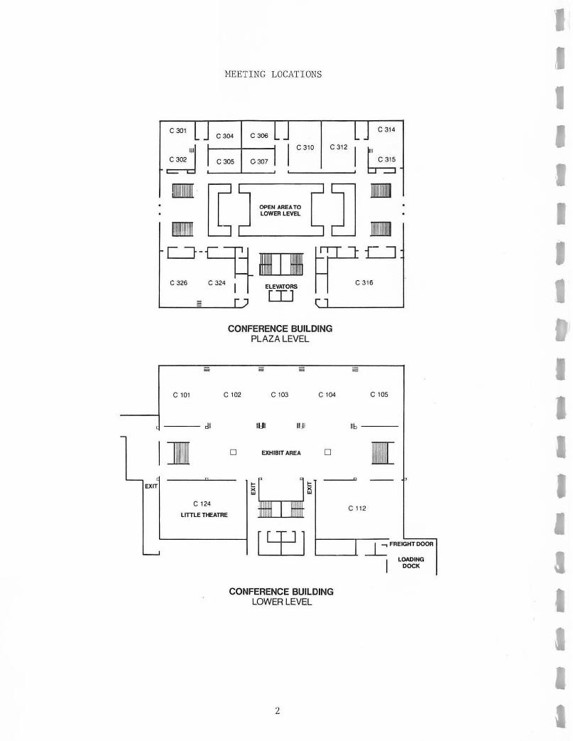
MAP: Meeting Locations
AGENDA
STATUS OF TECHNOLOGY TRANSFER
TECHNICAL SUMMARIES
CONTENTS
Project Analysis and Integration.
Silicon Material ••
Large-Area Silicon Sheet •
Encapsulation
Process Development Area •
Engineering
Operations •
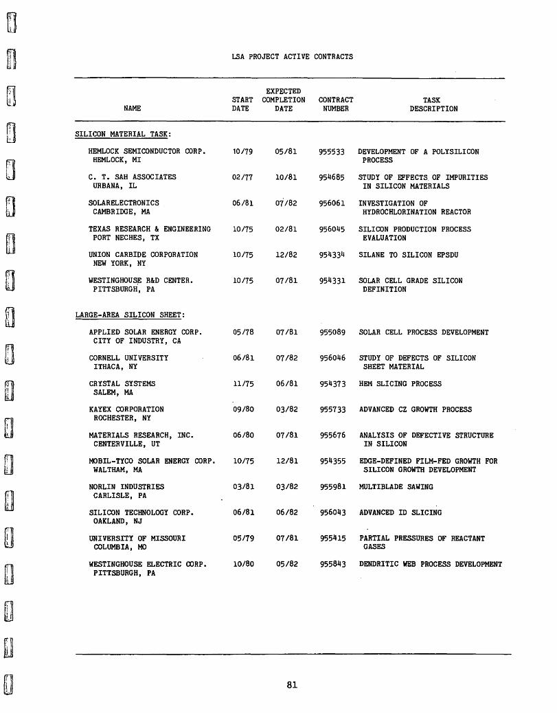
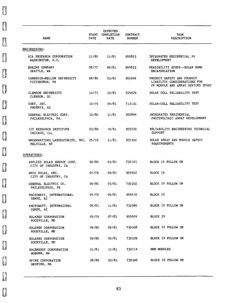
LSA PROJECT ACTIVE CONTRACTS.
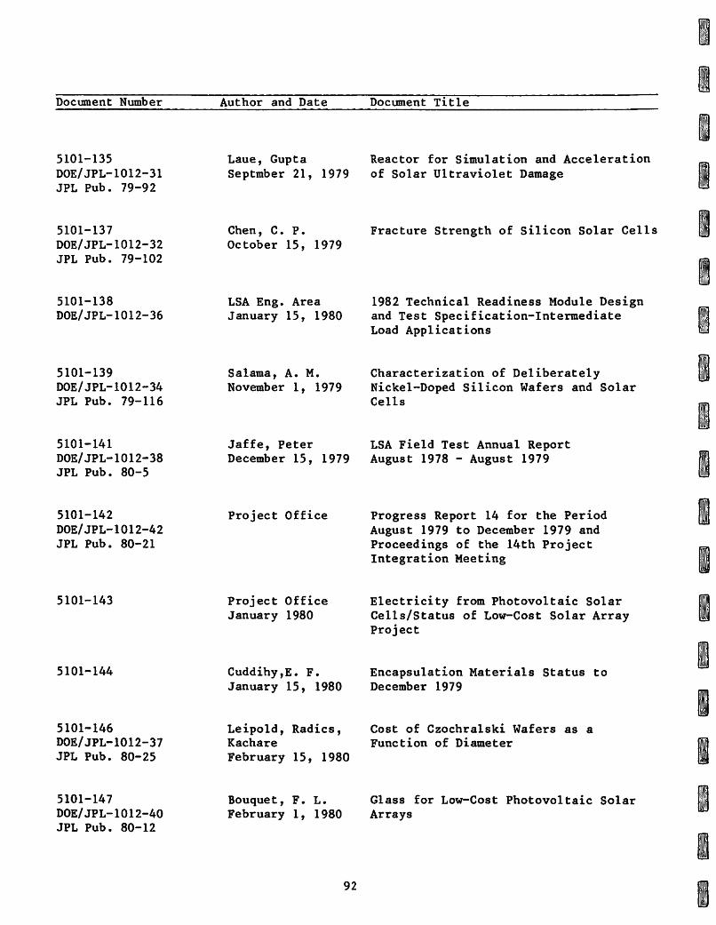
LSA PROJECT PUBLISHED DOCUMENTS
MAPS: Pasadena Area and Pasadena Center •
For Your Information
. .
. .
.
. . 1
. . 2
. . 3
. . 9
• 21
• • 21
. 27
• 39
• 45
. 57
• 69
• • • • 81
• 85
. • Inside Back Cover
Check-in: Please check in at the registration desk on the lower level of the conference building before the start of the meeting on Wednesday morning.
Telephone Messages: Incoming calls will be received at JPL on (213) 577-9520. Constant coverage of this phone will be provided and messages will be transmitted.
BADGES: We will appreciate your returning your badges at the end of the meeting. You will find deposit boxes at the lower-level exits.
iii
n n ~
n ~
e 0 ~ ~
0 0 a n ~
n
0 0
MEETING OBJECTIVES
The Low-Cost Solar Array (LSA) Project is convening its 18th Project Integration Meeting (PIM) at the Pasadena Center on July 15-16, 1981. Registration will begin at 7:30 a.m. on July 15, lower level of the Conference Building (see maps on following page and on inside back cover).
The theme for this PIM will be dual in nature - Perspectives for Progress and Module/Array Long Life Performance. We feel this dual theme is timely in view of the technical achievements to date. Viewpoints of the Project, Government, users and manufacturers will be given on today's status and future needs.
Emphasis is being placed on displays showing the current status of technical advancements.
It is requested that you bring this Handout to the meeting with you since we do publish a limited number.
1
MEETING LOCATIONS
• :Z:.uv C ::•., t. /,,,._, r S-,:, (.) fl f ...,_ n >'1:..5.
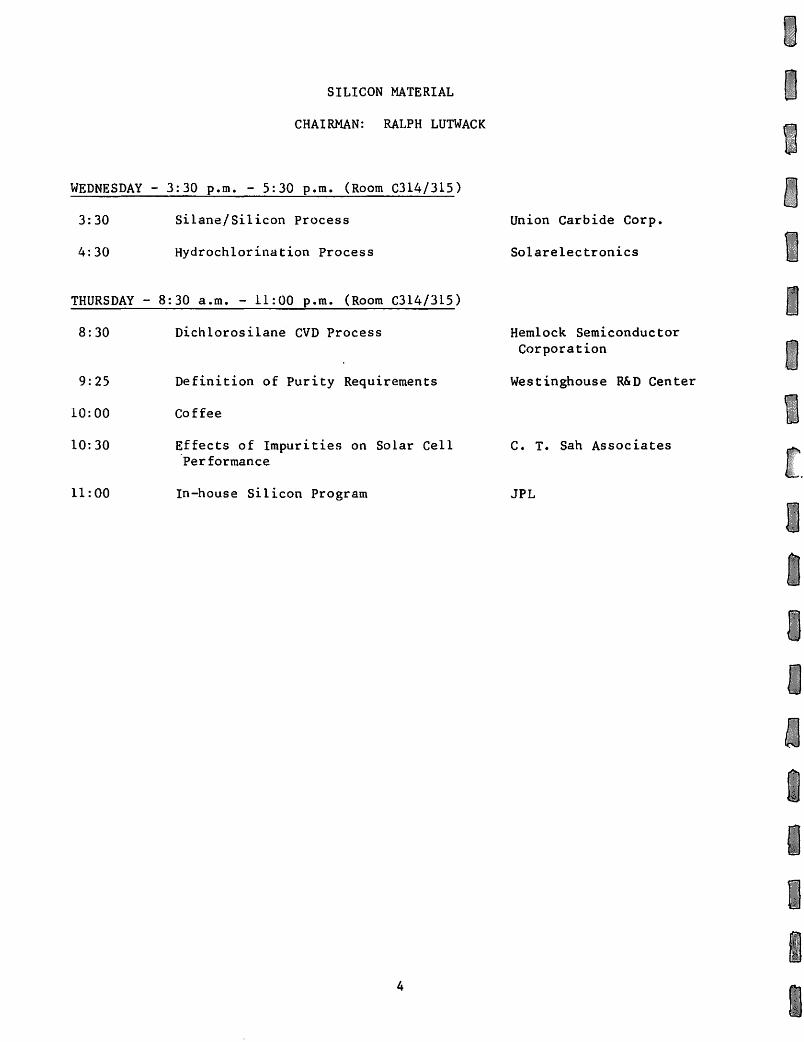
3: 30 Technology Sessions (Parallel) Silicon Material Large Area Silicon Sheet Encapsulation recess Development
Engineering/Operations
Quality Assurance Workshop
i$: 30 Social Hour
THURSDAY: July 16 1 1981
i,8':00 Technology Sessions (Parallel) Silicon Material Large Area Silicon Sheet Encaps ulation ~ ocess Development .
ll'E:ngineering/Operations
l.9~ 30 Coffee Available
!1£: 15 Lunch
u-f15 Parallel Activities Technology Transfer
i)(odule Reliability Forum ' Energy Payback Time , Spinoff Benefits,
Environmental Control Displays
i.f: 15 Coffee Available
\.t: 45 Looking in on Photovoltaics
3: 15 Summaries LSA Lead Center DOE
4:30 End of Meeting
..,
.J
EXHIBIT AREA (Lower Lobby)
ClOl ,. 3 w. Callaghan/L .T~~lJ,c,,}°r!;/},,;, ... ,.-r
ClOl /J :J M. Prince/ W. Callaghan ljQ min 5 min
ClOl I' ;I. R. Matlin (TriSolar) 50 min M. Brown (Az Pub Serv)
5 min
EXHIBI T AREA 20 min
ClOl
ClOl
ClOl F'L
ClOl
ClOl
J . Evans (JPL) 25 min 5 min
M. Wolf (Un . of PA ) 25 min 5 min
R. Ross (JPL) 25 min 5 min
.,---.....enl!, -t M .4£.«:-'7 ~-Hmt&. R. McGinnis (Photowatt) 55 min y ,(u,.;,; ta?."'1 12;.?#,v,.'U&J R. ~ xwell (Westinghouse) Dt.::Yt...--t., 'P,t4;_r,../7" - 6°,; 1 '7
I IA,';) WC/.!A:, N/JJ!t) a:.;,/J,<"1 min l='tJ,JDi -./G 0 ~0 f:l> 10/to Rn,,.:, rl?o,·,o~ Rnt<.. Rc.~ n· J . Liu (JPL) 25 min
ef:20 Comparison of US and Foreign Environmental Testing
ef:40 Inte r connect Fatigue Update
I-Y0:00 Hot Spot Thermal Modeling
il1l :15 Coffee
llrO : 30 Res idential Array Develo pment
.yf': 00 Residential Array Development
1.1.1' : 30 Array Safety Design
1-11'. : 50 Array Dynamic Wind Loading
t~ lS - 2:15 Special Open Session on Module Reliability
8
Forman
Runkle
Clemson
Clemson
Hoffman
Moore/Mon
Glaser
General El ectric
AIA
UL
Boeing
Ross, Runkle, Forman
I I I I I
I I I I I I I I I I I
n n
[]
n (]
a 0 n u
n ff/ ll}
a
STATUS OF TECHNOLOGY TRANSFER
The Production Process and Equipment Area is concerned with the transfer of technologies developed by the LSA Project for manufacturers of solar modules. The status of this transfer activity is reported periodically to provide an overview of processes available from JPL, and to promote experimentation, modification, and application. Inquiries and requests for process specifications should be directed to the LSA Project PP&E Area at (213) 577-9225.
Process
Texture Etching
Spray AR Coating
Etching Damage Removal
Texture Etching
CVD Si3N4
Surface Preparation
Contractor Status
Lockheed E
EP
Lockheed EP
Tracor MBA EP
Tracor MBA EP
Motorola EP
Evaluated Evaluation in Process Available Under Development Suspended
Surveyed By
General Electric Int'l Rectifier ARCO Solar Solar Power Univ. of PA
Solar Power Int'l Rectifier Spectrolab
Solar Power Int'l Rectifier
Solar Power ARCO Solar Int' 1 Rectifier
ARCO Solar Photowatt
14* 42 92
0 0
*Has been confirmed by at least one company
Comments
Confirmed Confirmed
Economic only
Status Code: E - Evaluated; EP - Evaluation in process; A - Available; D - Under development; S - Suspended.
9
I Surface Preparation (Cont) I
Process Contractor Status Surveyed By Comments I Plasma Damage Motorola E Westinghouse Confirmed I Etching
EP Solar Power ASEC I Spectrolab Univ. of PA Economic only
Wax Masking Motorola EP Solar Power I ARCO Solar Westinghouse
I Univ. of PA Economic only
Plasma Metal Motorola EP ASEC Pattern Definition ARCO Solar I Solamat
Texture Etch Motorola A
I Silicon Nitride Motorola A Deposition
I Spray AR Coating RCA E Photowatt Confirmed EP ARCO Solar
Solar Power I Spectrolab Westinghouse Univ. of PA Economic only
I Surface Prep. Etching RCA A
Megasonic Cleaning RCA A I Si3N4 AR Coating Photowatt EP ARCO Solar
Spin-On AR Coating Photowatt A I Texture Etching Photowatt E Lockheed Confirmed;
I req. mod. EP Solar Power
Univ. of PA Economic only
I Wafer Surface Photowatt EP Solar Power Preparation Univ. of PA Economic only
Surface Preparation Solarex EP ARCO Solar I Polish Etching Spectrolab EP ARCO Solar
I Rev. A
10 I
IJ .
I ll I 11 I I -I <
<
il '11
I I I <
i1 ti}
I 11 I I I Ir
Process
AR Coating
Dip AR Coating
Surface Preparation (Cont)
Contractor Status Surveyed By Comments
Spectrolab A
Westinghouse E ASEC Confirmed by Spin-on
EP ARCO Solar General Electric Solar power
11
I Junction Formation I
Process Contractor Status Surveyed By Comments I Ion Implantation Lockheed EP General Electric I
Univ. of PA Economic only
Laser Annealing Lockheed A I Aluminum BSF Tracor MBA EP Solec Int'l
ARCO Solar I Edge Etching Tracor MBA EP ARCO Solar
POClJ Diffusion Tracor MBA EP Solar Power I Ion Implantation Motorola EP ASEC
I Univ. of PA Economic only
Ion Implant, Motorola A N and P Type I
Drive-In Anneal Motorola A
POCl3 Diffusion RCA EP General Electric I Solar Power ARCO Solar
Ion Implantation RCA A I Plasma-Etch RCA A I Junction Edge
Laser Scribing Photowatt E Mobil Tyco Confirmed
I Spectrolab Confirmed Westinghouse Confirmed
EP ARCO Solar Univ. of PA Economic only I
POCl3 Photowatt EP ARCO Solar
Spray-on Dopants Photowatt A I Post-Diffusion Solarex EP ARCO Solar
I Cleaning
Junction Formation Solarex A
Al Printing Paste Spectrolab E Photowatt Confirmed I Rev. A EP Solec Int'l
ARCO Solar
I 12 I
n ti]
n n (I lfl1 u
a fil fU
ff1 u
0 a ITTl u
a ' (
0 a n tJ
a ' .
ITT) JU
Process
Laser Scribing
Polymer Diff. Wafer
Print and Fire BSF Rev. A
Remove Oxide and Clean Al Back Rev. B
Diffused Wafer
Ion Implantation Furnace Anneal
Spin-on Polymer Dopants
CVD p+
Junction Formation
Contractor Status
Spectrolab EP
Spectrolab E
Spectrolab E
EP
Spectrolab E
EP
Spectrolab A
Spire E
EP
Texas Inst. EP
Westinghouse EP
13
(Cont)
Surveyed By Conunents
ARCO Solar
Westinghouse Confirmed
ASEC Confirmed RCA Confirmed Westinghouse Confirmed ARCO Solar General Electric Photowatt
Photowatt Confirmed
Univ. of PA Economic only
Motorola Confirmed
RCA Confirmed General Electric Univ. of PA Economic only
Univ. of PA Economic only ARCO Solar
ARCO Solar
I I
Metallization
Process Contractor Status Surveyed By Comments I
Al Back Contacts ARCO Solar E Westinghouse Confinned I EP General Electric
Solar Power I Solec Int'l Spire Univ. of PA Economic only I
Thick Film Lockheed General Electric EP ARCO Solar
I Univ. of PA Economic only
Front Contact Tracor MBA EP Solar Power Fonnation I
Electroless Pd/Ni Motorola E ASEC Confirmed Photowatt Confirmed
I Solarex Confirmed Solar Power Confirmed Westinghouse Confirmed
(Mod.) I EP ARCO Solar NASA Lewis RCA I Spire Univ. of DE Economic only Univ. of PA Economic only
I Screened Wax Mask Motorola A Pattern
Electroless Nickel Motorola A I Plate
Metal Sinter Motorola A I Electrolytic Motorola A
I Copper Plate
Plate Copper ASEC EP ARCO Solar Westinghouse I
Thick Film RCA EP General Electric ARCO Solar I Spectrolab Univ. of PA Economic only
I 14 I
0 .
'
n a a a
a D 0 D fiJ tLJJ
D 0 fl u
a fJ ' .
D '
.
D
Process
Thick-Film Screen-Printed Metallization
Electroless Ni
Electroless Ni
Metallization
Mo/Sn Metallization System
Print and Fire Front Contact Rev. A
Silver Printing Paste
Midfilm
Metallization (Cont)
Contractor Status Surveyed By Comments
RCA A
Photowatt EP Solar Power Spire Univ. of DE Economic only Univ. of PA Economic only
Solarex EP Motorola ARCO Solar Solar Power Spire Univ. of DE Economic only Univ. of PA Economic only
Solarex A
Sol/Los EP Bernd Ross Solar Power
Spectrolab E Photowatt Confirmed EP ARCO Solar
General Electric Solec Int'l Univ. of PA Economic only
Spectrolab EP ARCO Solar
Spectrolab A
15
Process
Elec. Test and Sort
Framing
Lamination
Module Layout and Interconnect
Cell Test
Double Glass
Cell Test
Cell Matrix
Encapsulation
Module Test
Mass Soldering
Interconnect and Encapsulation
Tabbing
Testing
Apply & Cure Conformed Coating
Applying Inter-connects
Cell Test
Circuit Assembly
Final Test
Frame Module
Interconnect Cells
Module Assembly
Contractor Status
Tracor MBA EP
Tracor MBA EP
Tracor MBA EP
Tracor MBA EP
Motorola A
RCA A
RCA A
RCA A
RCA A
RCA A
RCA EP
Solarex EP
Solarex A
Solarex A
Spectrolab A
Spectrolab EP
Spectrolab EP
Spectrolab A
Spectrolab EP
Spectrolab A
Spectrolab A
16
Surveyed By
ARCO Solar Wyle Labs
Solar Power
Solar Power
Solar Power
Solar Power
Solar Power ARCO Solar
ARCO Solar
Wyle Labs
ARCO Solar Wyle Labs
Comments
I I . .
I I
I I I I I I I I I I I I
n I I
n '
I
fl
a [J
a [J
a a
fl u
[l
[J
a a
Module Assembly
Process Contractor Status Surveyed By Comments
Laminate Circuit Spectrolab EP Tracor MBA
Lead Cell Spectrolab A
Mount Cells on Spectrolab EP Wyle Labs Superstrate & Cure Adhesive
Mount Superstrate Spectrolab A in Frame
String Assembly Spectrolab A
Tin Solder Pad on Spectrolab EP ARCO Solar Back Al
Vacuum-Bag Fabrication Springborn EP ARCO Solar
17
TECHNICAL SUMMARIES
n u
a
a I
.
n LI
a
[] I .
n u
In-House Program
SILICON MATERIAL TASK
Jet Propulsion Laboratory Pasadena, California
The objective of this effort is to provide support to the Silicon Material Task in selected critical areas.
To serve as a basis for an experimental program using a six-inchdiameter fluidized bed reactor (FBR), a series of experiments was run in a two-inch-diameter FBR. The study dealt primarily with silicon fines formation and agglomerations. Tests at high silane concentration, including 100% silane, were conducted successfully without bed agglomeration and with less than 10% fines. These results are significant in that they may aid considerably in achieving lower silicon cost by means of increased throughput, since FBR operation with 10 mole% silane in hydrogen has already been shown analytically to be economically attractive.
The silane-to-molten-silicon converter was modified to serve as a 1700°C reactor for rapid experimentation.
In the task for the analysis of impurities using thermally stimulated capacitance (TSCAP) measurements, effort was spent on automating the equipment using a calculator-controlled system. The system has been programmed for the measurement of trap concentrations •
In the effort on consolidation of sub-micron silicon powder, the powder compactor/extruder, which feeds the material to the melter, was modified and successfully operated.
Approval Signature Date
21
SILICON MATERIALS TASK
HEMLOCK SEMICONDUCTOR CORPORATION
HEMLOCK, MICHIGAN 48626
Contract Title: Development of a Polysilicon Process Based on Chemical
Vapor Deposition
Contract No. : 955533
The objective of this program is to demonstrate the feasibility of a chlorosilane based chemical vapor deposition process for the production of a low cost-high purity polysilicon. Efforts are currently being expended in the following technical areas:
The experimental reactor feasibility and optimization programs have been successfully completed. The feasibility of generating high purity silicon from DCS with high conversion and energy efficiencies has now been well established.
An intermediate-sized production reactor (Model 8D) has been modified for accepting dichlorosilane-hydrogen feed with the DCS supplied in 250 lb. cylinders. Prior to reactor operation, explosion tests were conducted on the quartz bell jar - metal heat shield to insure that under a worst case condition {DCS-H2 -Air mixture ignited in the bell jar) that the heat shield would contain the explosion. The explosion tests demonstrated the adequacy of the heat shield design.
A remote cylinder feed system has been constructed for providing DCSH2 to the Model 8 reactor. The reactor cylinder feed system has been operated successfully on four run segments which confirmed on a larger scale the data collected with the small experimental reactor.
Construction of the dichlorosilane production system (DCS-PDU) capable of producing dichlorosilane at rates up to 100 lbs/hr. has been completed along with all safety audits. System purging has been completed and modification of a second Model 8D reactor is in progress. Integrated PDU-Model 8D reactor is scheduled for June.
Several grades of trichlorosilane were evaluated to establish a feed material with adequate purity to be fed to the DCS-PDU. A suitable TCS source was found at HSC to permit PDU operation without potential contamination of other process streams with which the PDU is integrated.
A preliminary EPSDU design has been completed which would demonstrate all aspects of the HSC dichlorosilane process except hydrogenation and trichlorosilane purification.
<~- ~ /~ ~~~ c£ t 1q.·;1 ,A
Approval Signature
22
~ Jt}rJE_ ~ l
Date
I I I I I I I -
I I I I I ll I I I I I I
n tB
a
a
a . .
~ . .
u ' .
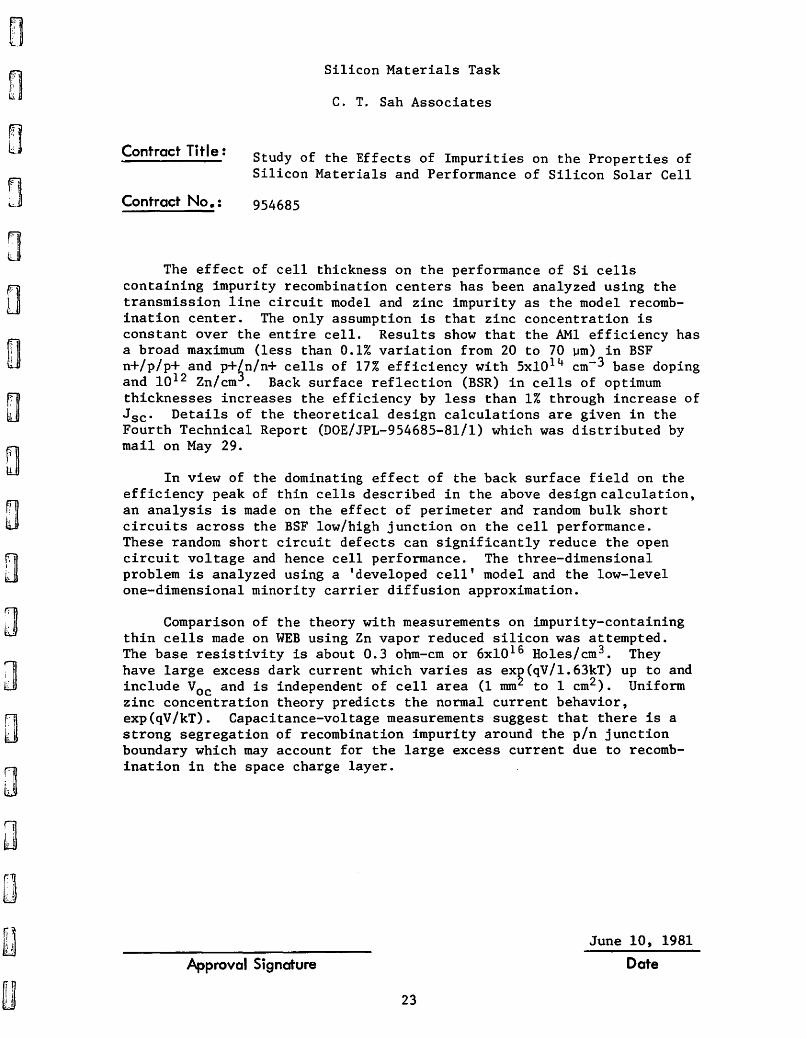
Contract Title:
Contract No. :
Silicon Materials Task
C. T. Sah Associates
Study of the Effects of Impurities on the Properties of Silicon Materials and Performance of Silicon Solar Cell
954685
The effect of cell thickness on the performance of Si cells containing impurity recombination centers has been analyzed using the transmission line circuit model and zinc impurity as the model recombination center. The only assumption is that zinc concentration is constant over the entire cell. Results show that the AMl efficiency has a broad maximum (less than 0.1% variation from 20 to 70 µm) in BSF n+/p/p+ and p+[n/n+ cells of 17% efficiency with 5xl014 cm-3 base doping and 1012 Zn/cm3. Back surface reflection (BSR) in cells of optimum thicknesses increases the efficiency by less than 1% through increase of Jsc· Details of the theoretical design calculations are given in the Fourth Technical Report (DOE/JPL-954685-81/1) which was distributed by mail on May 29.
In view of the dominating effect of the back surface field on the efficiency peak of thin cells described in the above design calculation, an analysis is made on the effect of perimeter and random bulk short circuits across the BSF low/high junction on the cell performance. These random short circuit defects can significantly reduce the open circuit voltage and hence cell performance. The three-dimensional problem is analyzed using a 'developed cell' model and the low-level one-dimensional minority carrier diffusion approximation.
Comparison of the theory with measurements on impurity-containing thin cells made on WEB using Zn vapor reduced silicon was attempted. The base resistivity is about 0.3 ohm-cm or 6xl0 16 Holes/cm 3 • They have large excess dark current which varies as ex~(qV/1.63kT) up to and include V0 c and is independent of cell area (1 mm to 1 cm2 ). Uniform zinc concentration theory predicts the normal current behavior, exp(qV/kT). Capacitance-voltage measurements suggest that there is a strong segregation of recombination impurity around the p/n junction boundary which may account for the large excess current due to recombination in the space charge layer.
Approval Signature
23
June 10, 1981
Date
SILICON MATERIAL TASK
UNION CARBIDE CORPORATION
Tonawanda, New York 14150
Contract Title: Silane-to-Silicon EPSDU
Contract No.: 954334
Construction of the lOOMT/Yr EPSDU at East Chicago, Indiana is continuing. All civil and structural work is complete. The bulk of equipment has been delivered to the EPSDU site, and most major equipment pieces have been inspected and placed in position.
The mechanical installation bid package was sent to potential subcontractors, and a job site meeting was held with them in May to explain the scope of the work. It includes installation of all equipment, piping, tubing, insulation, power wiring, and instrumentation wiring. Bidders are expected to return the bid in late June. The electrical installation bid package is in preparation and will be sent to potential bidders by early July. Due to a FY81 funding recision, awarding of the installation subcontracts will probably be delayed until sufficient funds become available.
Helter subcontract work with Kayex Corporation is proceeding on schedule towards completion in September. The silicon shatter was assembled and an initial series of tests with chunk silicon was successful. Chunk silicon was melted in a quartz crucible having a small aperture on the bottom. The aperture sizes tested ranged from 0.7 to 2.0 mm in diameter. The melted silicon, in the form of shot, dropped through the crucible aperture and substantially solidified in the cooling drop tower during free fall. Kayex plans to feed free-space reactor powder to the shatter in June.
The fluid-bed pyrolysis PDU was assembled and an initial series of tests was also successfully completed. Ten to twenty percent silane in hydrogen was fed to the silicon seed bed during a four-hour run. A visual inspection of the bed after the run indicates that the particle morphology appears excellent and little undesirable silicon powder was produced. This program was stopped in mid-May due to FY81 funding recision.
Overall, all phases of the EPSDU program have been progressing successfully. The only significant technical problem, the shatter system, is close to solution.
~~ Approval Signature
24
I I .
I I I [I
I I [I
I I I I I I I I I I
n
[J tn u , [J
a
a
a a I .
u '
.
ITT] u
SILICON MATERIALS TASK (Part 2)
Westinghouse R&D Center/Dow Corning Corp.
Pittsburgh, PA 15235
Contract Title: INVESTIGATION OF THE EFFECTS OF IMPURITIES AND PROCESSING
ON SILICON SOLAR CELL PERFORMANCE
Contract No.: 954331
The objective of this program is to determine the effects of impurities, processing and impurity-process interactions on the properties of silicon and silicon solar cells so that impurity limits for solar grades of silicon can be defined and cost-benefit tradeoff can be made by the users of this cheaper, less pure silicon.
The current phase IV effort is now essentially complete. It included five major tasks: (1) evaluation of experimental silicon materials, (2) investigation of impurity effects in polycrystalline devices (3) identification of impurity thresholds for high efficiency cells (4) assessment of process effects such as ion implanting on impurity-doped devices and (5) an extension of studies to identify long term impurity effects.
We confirmed (at least for V, Mo and Cr) that impurity-induced structural degradation in polycrystalline silicon ingots takes place at lower liquid impurity concentrations than when growing single crystal ingots under comparable freezing conditions. The threshold imiurity concentration for breakdown of a smooth crystal-liquid interface, c1 , is 2 to 10 times smaller for polycrystalline than for single crystal ingots.
Using a model relating the measured value of cf to experimental growth parameters we calculated the value of the liquid impurity diffusion constants for Gd,Zr,Mo,W,V,Ti,Fe,Co,Pd,Ag and Cu in silicon. Dt ranged from 1.5 to 4.2xlQ-4 cm2/sec these elements; the values are similar to those reported for other metals in liquid silicon.
Ar implant damage combined with HCt or POCt3 gettering raises the efficiency of Ti-doped solar cells by 0.5 to 1% (absolute) compared to ungettered devices. Ar implant damage plus heat treatment alone at 1100°C also raises cell efficiency but not as much as for the combined treatment. The most effective gettering treatment for Ti still appears to be high temperature reaction in HCi alone or POCt
3 alone. For Cu-doped cells none
of the gettering treatments (implant damage plus HCt or POCi3, implant damage plus heat treatment, or HCi/POCt3 alone) raises cell efficiency to that of the ungettered devices.
Extensions of the impurity performance model to high efficiency devices indicate that 1) impurity tolerance is less in high efficiency devices than our conventional n+p devices and 2) that this impurity sensitivity can be reduced by using thinner high efficiency cells. Experimental data from lOOum thick BSF cells made on V-doped silicon support these predictions.
'/~/r, Date
25
n n a
a n a
a
a I
.
Pl u
[] ' .
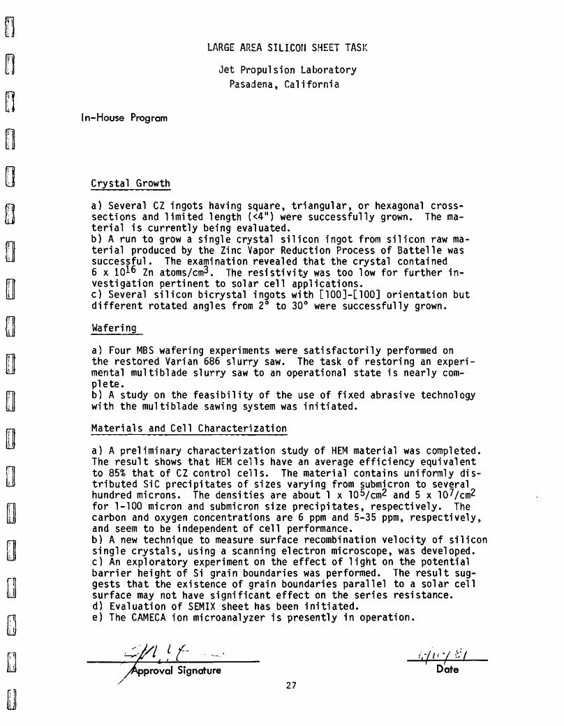
In-House Program
Crystal Growth
LARGE AR:::A SILI.COrl SMEET TASK
Jet Propulsion Laboratory Pasadena, California
a} Several CZ ingots having square, triangular, or hexagonal crosssections and limited length (<4 11
} were successfully grown. The material is currently being evaluated. b} A run to grow a single crystal silicon ingot from silicon raw material produced by the Zinc Vapor Reduction Process of Battelle was successful. The examination revealed that the crystal contained 6 x 10¹⁶ Zn atoms/cm3. The resistivity was too low for further investigation pertinent to solar cell applications. c} Several silicon bicrystal ingots with [100]-[100] orientation but different rotated angles from 2° to 30° were successfully grown.
Wafering
a) Four MBS wafering experiments were satisfactorily performed on the restored Varian 686 slurry saw. The task of restoring an experimental multiblade slurry saw to an operational state is nearly complete. b} A study on the feasibility of the use of fixed abrasive technology with the multibl.ade sawing system was initiated.
Materials and Cell Characterization
a} A preliminary characterization study of HEM material was completed. The result shows that HEM cells have an average efficiency equivalent to 85% that of CZ control cells. The material contains uniformly distributed SiC precipitates of sizes varying from submicron to several hundred microns. The densities are about 1 x 10⁵/cm2 and 5 x 10⁷/cm2 for 1-100 micron and submicron size precipitates, respectively. The carbon and oxygen concentrations are 6 ppm and 5-35 ppm, respectively, and seem to be independent of cell performance. b) A new technique to measure surface recombination velocity of silicon single crystals, using a scanning electron microscope, was developed. c} An exploratory experiment on the effect of light on the potential barrier height of Si grain boundaries was performed. The result suggests that the existence of grain boundaries parallel to a solar cell surface may not have significant effect on the series resistance. d} Evaluation of SEMIX sheet has been initiated. e} The CAMECA ion microanalyzer is presently in operation.
' I Date proval Signature / 27
I LARGE AREA SILICDN SHEEr TASK
APPLIED SOI.AR ENERGY CORPORATION I City of Industry, California
Contract Title : SILICON SOI.AR CEl.L PROCESS DEVEIDPMENT, FABRICATION AND ANALYSIS I Contract No. : 955089
The objective of the program is to investigate, develop and utilize technologies appropriate and necessary for improving the efficiency of solar cells made fran various unconventional silicon sheets. Silicon sheets under evaluation included HEM (Crystal Systans), Dendritic Webs (Westinghouse) and SEMDC (Solarex) •
Two large HEM ingots (12" x 12" x 6" 1 == 40 kg) were sectioned and sliced to prepare for substrates. Baseline solar cells ( 2 x 2 cm) were fabricated and detaila:l mappings of the cell perfonnance, as a function of the blanks location within the ingots, were obtained.
Baseline solar cells were fabricated from dendritic webs precharacterized by MRI (Utah) • Efforts were made to correlate defect densities with solar cell parameters.
Several sliced SEMIX wafers (10 x 10 cm, 10 - 16 mils thick) were delivered to ASEC. Baseline solar cells were fabricated and performance results will be presented.
Approval Signature
28
June 12, 1981 Date
I I I I I I I I I I I I I I I I
n ml filj
a
a Wl) u
[I fTI AtJ1
n tJj
f1 ~
LARGE AREA SILICON SHEET TASK
CORNELL UNIVERSITY
ITHACA, NY
Contract Title: Characterization of Structural, Electrical and Chemical Properties of Silicon Sheet Material.
Contract No. : 954852
In the period 12/31/80 to 6/12/81 the following work was carried out:
(a) EBIC investigation of SOC The structure and electrical activity of grain boundaries in SOC material is similar to that of EFG material. In the samples studied so fa~ electrically active higher order twins and grain boundaries are present to a somewhat higher (about a factor 1.5) amount than in EFG.
(b) EBIC investigation of HEM HEM contains few boundaries. Those boundaries that do exist are largely coherent twins, most of which are not electrically active. Some of the coherent twins show partial activity (dotted contrast) conceivably due to the presence of secondary dislocations or of pre cipitates (TEM is being carried out to answer this question). The remaining boundaries are higher order twins and high angle grain boundaries both of which are electrically active. Intersecting twins show electrical activity in the region where they joined, even when of the same crystallographic orientation.
(c) High resolution TEM of RTR feedstock. RTR CVD feedstock contains a high density of twins and other boundaries, and is therefore a convenient material to study the structure of higher order twins with high resolution (lattice images) microscopy. We find that third order twin boundaries (Sigma 27) consist of a second order (Sigma 9) boundary which is located next to a stepped first order coherent (Sigma 3) boundary. The two boundaries are separated by 5 - 10 Angstroms and therefore appear in regular TEM (and other analytical methods) as a single third order boundary.
this contract is for casting silicon ingots by the Heat Exchanger Method (HEM) and slicing by multi-wire Fixed Abrasive Slicing Technique (FAST).
The emphasis of the present program is to characterize HEM cast ingots of 30 cm x 30 cm x 15 cm weighing 35 kg. Two such ingots have been thoroughly characterized by JPL. It was concluded that the overall efficiency of the usable material averaged throughout the ingot is 85% of the control cell CZ material. It was felt that SiC precipitates and high dislocation density may be factors limiting solar cell efficiency. The source of SiC has been traced to backstreaming of oil vapors from the mechanical pump into the chamber. Efforts in reducing the backstreaming of oil vapors has produced a very bright metallic appearance of the ingots. These ingots will be characterized for SiC. The high dislocation density observed in the first two ingots is being corrected by altering the cooldown cycle.
During last PIM it was reported that it is possible to slice 10 cm diameter silicon ingots at 25 wafers/cm with FAST; however, the yields were low. It has now been demonstrated that the yields can be as high as 99.1% (222 out of 224); the average slicing rate was 3.03 mils/min (0.077 mm/min). In another slicing test the yield was 88% (197 out of 224) and the average slicing rate was 2.4 mils/min (0.061 mm/min). This has been achieved by using in-house fabricated wirepacks electroplated with 30 µm natural diamonds over the entire circumference of the wires. A similar wirepack spaced at 25 wires/cm and electroplated with 45 µm natural diamonds showed an average slicing rate of 3.6 mils/min (0.091 mm/min).
Slicing of 15 cm diameter silicon ingots has also been accomplished at 19 slices/cm with an average slicing rate of 2.9 mils/min (0.074 mm/ min). This was achieved by using electroforming techniques to fix 60µm diamonds on wirepacks in the cutting edge of the wires with the electroplated layer subtended an arc of only 60°. Even with such large diamonds it was, therefore, possible to control the kerf to less than 8mils (0.2 mm). With such large kerf length broken pieces of wafers were trapped which caused low yields.
A tungsten core wire was used because of its high modulus and corrosion resistance. Earlier attempts to use high strength steel showed embrittlement problems. By altering the chemical composition of the plating baths and baking of wirepack after plating, a steel core wirepack has now been used to slice three 10 cm diameter silicon ingots.
.. Cl, A .. -4'-~ I! la~~, /.------------------Approval Signature
30
June 9 1 1981 . Date
I I I I I I I I I I I I I I I I I I I
f1l fu.j)
a ITT} IJ
a []
a a n iJ
~
Contract Title:
Contract No. :
Large Area Silicon Sheet Task
Kayex Corporation Rochester, NY
Development of an advanced Czochralski growth process to produce low cost 150 kg silicon ingots from a single crucible for technology readiness. 955733
JPL contract number 955733 was issued in September, 1980. The contract includes construction of a crystal grower and process development on advanced czochralski including demonstration of technology readiness rapidly transferrable to industry.
To date, the modified CG 2000 RC crystal grower has been installed and the process development phase commenced. A total of seven crystal growth runs have been made in order to successfully establish operating parameters. 150 kg multiple recharge growth runs will first utilize a 15-inch diameter crucible, and subsequently a 16-inch diameter.
The modified CG 2000 RC grower will be equipped with a KayexHamco Automatic Grower Logic (AGL) computer control system. Tasks within this contract address the development of sensors for use with the AGL system to enhance its capability for volume production of solar cell material. To date, sensors for dip temperature setting and automated crown growth have been implemented. Integration of the computer and sensors with the grower is scheduled for July.
Procurement and assembly of the gas chromatography equipment for the analytical study phase of the contract is complete. The system is currently being calibrated prior to interfacing with the crystal grower.
Approval Signature Date
31
Task II - Large Area Silicon Sheet Task
Materials Research, Inc.
Centerville, Utah 84014
Contract Title: Analysis of Defects Structure in Silicon
Contract No. : 955676
The objective of this work is to evaluate and, predict the conversion efficiency of a variety samples with differences in structural defects grain boundaries, twin boundaries, precipitate dislocation density, etc.
if possible, of silicon such as particles,
Some of the dendritic web samples analyzed earlier by MRI have now been fabricated into solar cells. Results show godd agreement between defect densities in these samples and observed conversion efficiency of the cells. During the reporting period, fifteen (15) Mobil Tyco EFG samples were analyzed by Quantimet 720 Image Analyzer (QTM 720). In addition, twenty two (22) Honeywell SoC samples were also analyzed. The surfaces of the Soc samples were very irrPgulnr. Aftrr considernblc effort, procedures were developed and perfected for the polishing, etching, and analysis of the samples. Analysis on these samples have been completed. In addition, 70 HEM coupons were also analyzed during this period. Detailed reports on the examination of these samples are being prepared and will be sent to JPL shortly.
,-:> c.a, ...
Approval Signature
32
J ... : ··,·~ g; I '18 I
Date
I I I I I I I I I I I I I I I I I I I
fil [j
a a
[!11 ljJ
fi~ WJ
Contract Tit I e :
Coni ract No.:
LARGE AREA SILICON SHEET TASK
Mobil Tyco Solar. Energy Corporation Waltham, MA 02254
LARGE AREA SILICON SHEET BY EFG
954355
A new program plan has gone into effect as of March 1, 1981, which calls for the design, construction and testing of a new multiple ribbon furnace at Mobil 'Iyco's expense, and for introduction of this unit into the LSA program in the last quarter of 1981. This unit will provide for simultaneous growth of four 10 cm wide ribbons with continuous melt r~plenishment and automatic width control. The goals for the new multiple ribbon furnace for 1981 are to achieve simultaneous growth of four 10 cm wide ribbons at a speed of 4 cnv'minute in a demonstration run of eight hours; cell efficiency. is to be 10.2%. support work in the existing multiple ribbon Furnace 16 and single ribbon Furnaces 17 and 18 is to continue on optimizing growth conditions at 4 cnv'minute and material quality to deJtonstrate large area (50 cm2) cells of 12+% efficiency by the end of 1981.
Construction of the new four ribbon furnace is in its initial stages. Finalization of all aspects of design has been completed except for the details of the main zone heater and of the cartridge. Input toward the final design of these components will continue to be received from Oir eration of the other furnaces in the program until about September.
The most successful three 10 cm cartridge demonstration run to date was achieved in Furnace 1.6 in March, 1981. Simultaneous full-width growth of three ribbons was carried out for 47% of the time over the eighthour duration of the experiment, with growth speeds between 3.2 and 3.6 crq/minute. ·
Experimental work in the single cartridge Furnaces 17 and 18 has continued to investigate factors that lirni t growth speed and influence quality of the 10 cm wide ribbon in the 3 to 4 cnv'minute growth speed range. This effort is proceeding along two distinct paths. Furnace 17 ,is being operated to optimize growth and quality with the existing 10 cm cartridge with cold shoes, while development of a· growth system for 10 cm wide ribbon without the conventional design of cold shoe has been started in Furnace 18.
Date
33
LARGE AREA SILICON SHEET TASK
P.R. Hoffman Division of Norlin Industries, Inc.
Carlisle, PA 17013
Contract Title: Multiple Blade Sawing (MBS) of Silicon Ingot Into Sheet:
Testing and Development
Contract No.: 955981
Since the close of Contract No. 955563 in May, 1980, P.R. Hoffman has continued to pursue solutions to the design and economic problems associated with wafering of silicon ingot. Through continued close communication with the JPL technical staff, both JPL and P.R. Hoffman have been kept aware of progress being made and additional concerns.
The current contract (#955981) requires that P.R. Hoffman provide optimization of the saw design and the MBS process via prototype research of the wafering process and investigation of several potential means of cost reduction. Since receipt of the contract in March, 1981, we have embarked on a carefully developed schedule of tests which will resu 1 t in base 1 ine information to be used in improving process cutting rate and wafer yields.
Research of the potential for reclaim and recycle of vehicle and abrasives has begun and is proceeding on schedule. Also underway is the design of a wafer lift-off device for removal of completed wafers from the saw and transport to the subsequent cleaning process.
As the 18th Project Integration Meeting will occur early in the contract period,we do not anticipate the announcement of a major breakthrough in MBS technology at that time. We do anticipate the ability to report some small reduction in the wafering add-on cost as compared to that reported in May, 1980.
I . r,> I k.,· - / I-· • J
' Approval Signature Date
34
I I I I I I I I I I I I I I I I I I I
'11 lJ
a
a (I
a
[TI Lil
LARGE AREA SILICON SHEET TASK
SEMIX INCORPORATED Gaithersburg, Maryland
Contract Title: "Semicrystalline Casting Process Development and Verification"
Contract No.: DE-FC01-80ET 23197
"Semicrystalline Casting Process Development and Verification" is a three year Cooperative Agreement between Semix and the United States Department of Energy. Phase I of this program ended June 19, 1981 and has successfully developed the technologies and proven the economies needed to demonstrate commercial readiness of a silicon sheet manufacturing process compatible with the Department of Energy price goal of $2.80/Wp.
Work to be presented at this Project Integration Meeting will concentrate on the following areas:
1) Proof-of-Concept - A discussion of crystallographic order in semicrystalline material as it affects cell performance
2) High Temperature Systems Development - The characterization of 140 runs and several thousand fabricated large area cells in relationship to operating conditions
3) Wafering and Mechanical Systems - The best-to-date results on MBS and ID sawing including the implication of these results for economic projections
4) Auxiliary Systems - A description of the data information system and the types of equipment inputs
5) In addition, revised SAMICS inputs have been prepared. Assumptions, inputs and results will be presented.
With the successful demonstration of commercial readiness the program will now concentrate all efforts directly on developing those parts of the semicrystalline casting process which are needed to demonstrate technology readiness to meet the DOE 1986 price goal of $0.70/Wp.
,,. ,. /( , ! .,•.,' I ! \ ,,- ./ : ··.·,
/~ . /1 l.'~
Date
./
' Approval Signatur~
35
SHEET TASK
SILICON TECHNOLOGY CORP.
OAKLAND, NJ
Contract Title: I • D. WAFER I NG OF SI LI CON FOR SOLAR CELLS
Contract No. : FY-73O105
The purpose of this contract is to develop and evaluate techniques for slicing of 150 mm single crystal and 100 mm square cast ingots.
During the preceding quarter, we have sliced square cast ingots at 25 wafers per cm. and 150 mm ingots at 17 wafers per cm .. The square wafers were automatically retrieved and were loaded into a cassette. Slicing speeds were about 1.5 inches per minute on the 150 mm wafers, and generally less than 1-inch per minute on the very thin square wafers.
Blade kerf was reduced to 0.27 mm for the 10 cm. wafers. Wafer yield and thickness varied among different manufacturers of square cast ingots. Some ingots were cracked and showed internal stress, which made wafering very difficult.
&:l- ~~-<-.-t;-<-7=-
Approvol Signature
6. ·- s:·- ~ I Dote
36
I I I I I I I I I I I I I I I I I I I
n n
[J
a a a •
a a a I :
LARGE AREA SILICON SHEET
Westinghouse Research and Development Center
Pittsburgh, PA 15235
Contract Tit I e : ADVANCED DENDRITIC WEB GROWTH DEVELOPMENT
Contract No. : 955843
Width control of silicon web growth has been developed such that long web crystals of specified width, constant to within a few tenths of a millimeter, may be grown routinely. Only very infrequent operator attention is required and inexperienced operators have grown crystals of controlled width to three centimeters. Control is attained through use of passive thermal shields which required no adjustment or control circuitry. Modifications embodying this concept are underway in order to grow wider crystals at constant width.
Automatically progranuned start of web growth has been attained by interfacing a Leeds and Northrup 1300 Process Progrannner with the temperature and pull speed control systems of a silicon web furnace. A predetermined sequence of these parameters has demonstrated reproducible, high quality web crystal starts, thus eliminating an operator function which normally requires some degree of skill. This development and the above-mentioned width control greatly reduce the operator time and skill requirements for web growth.
Development of techniques for the enhancement of web growth area throughput rate continued through a coordinated experimental and computer modeling effort. A computer analysis of stress and buckling, a width limiting effect, has been given a preliminary verification and found to predict growth deformation within 5% of the experimentally observed value. This procedure is now being used to evaluate the stress properties of assumed temperature profiles which will then be used to guide the fabrication of growth hardware. In a related development, thermal design modifications have been used to enhance growth speed while also decreasing stress and improving crystal quality.
Design of a prototype web growth machine having the cost and features identified by economic analysis has been essentially completed. The machine is now being fabricated with completion expected in August. In addition to many cost reductions, the new design includes functional design improvements. Among the functional improvements is new circuitry for the control of the melt replenishment system. This improvement provides continuously variable control of the polysilicon feed rate and is insensitive to variations in the laser beam intensity.
Approval Signature Dote
37
~ .
j
a rl Ul
a ~ I
.
'
a . .
ENCAPSULATION TASK
Jet Propulsion Laboratory
Pasadena, California
In-House Program Material Durability and Life Assessment
Develooinq quantitative relationships that relate environmental stress such as solar ultraviolet, wind, temperature extremes, and moisture to the rate of degradation of module performance and structural integrity are objectives of the Encapsulation Task in-house efforts. These activities are integrated with contractual activities to develop an over-all module lif~ prediction method.
Photothermal degradation rates and mechanisms and ultraviolet absorption characteristics of polymeric encapsulants are being measured as a function of polymer composition and test exposure conditions. Data are being obtained for silicones, EVA, P-nBA, polyurethane, EMA, PVB, and acrylic films. Failure mechanisms and critical temperature limits associated with module hot cell experience are being identified for use in establishing module circuit design and diode protection criteria.
Encapsulation material degradation data for low-cost advanced encapsulant systems is being gathered using various test hardware such as mini-modules {12 11 x 16 11
), two-cell modules and individual material samples. Exposure facilities include JPL laboratory test chamber and selected California field test sites at Point Vicente, JPL, Goldstone, and Table Mountain.
A JPL-LSA Report 5101-177 has been written which describes the module encapsulant material requirements for the various functional elements of a complete photovoltaic module encapsulation package. This information is presented in terms of material properties, performance, life and cost requirements. It describes the status and availability of potential material and process candidates with criteria and guidelines for their selection, processing, and optimizing configurations for specific applications.
New material products tailored to the specific requirements defined and publicized by the LSA Project for PV module encapsulation are now available from DuPont and 3M for the PV Manufacturers. These products include non-blocking EVA film in production quantities, iaminated EVA/Tedlar sheets, and PMMA UV-screening cover films.
~~~p~ proved Signature
~I0,118/ :J Date
39
Encapsulation Task
Illinois Tool Works, Inc., Venture Group
Elgin, IL
Contract Title: Ion Plating of Solar Cell Arrays
Contract No.: 955506
The ITW contract was initiated in December 1979 to investigate, develop and demonstrate the capability to produce operational solar cells having metallizations and AR coatings deposited by gasless ion plating, which will separately and/or in combination with a low cost encapsulation system meet the LSA project life, cost and performance goals.
Since February, work at ITW has been concentrated on producing cells with ion plated metallizations, having efficiencies as good as "control" cells made from the same batch of silicon with conventional metallizations. Contact masks were cut from .008" thick steel shim stock to delineate a front electrode pattern utilizing a two bus bar system with .011" wide collector fingers ('vl0% area of coverage on the front of the cell). The cells were fabricated from 100 mm dia., 'v5mm thick Pon N type wafers supplied by Solar Power Corporation, with control cells coming from Solar Power's regular production. Ion plated metallizations consisted of a nickel-copper front electrode pattern and a titanium-copper back contact. Results indicated that the ion plated metallizations were too thin to meet the conductivity requirements of the bus bars, so these cells were solder dipped to build up the conductor's thickness. The average efficiency of these cells (solder dipped with a copper-Invar bus bar strip) was 'vll.9% with a range of 10.6 to 12.8% (controls ranged from 11.1 to 11.9%). Although the power output of the ion plated cells often exceeded that of the control's, the diode fill factor (an indication of junction quality) was somewhat lower, being 79 to 81% for the controls and 77 to 79% for ion plated cells. The origin of this phenomenon is currently under investigation. Also, a program to produce cells from Non P wafers is under way.
~i/wrnfl...e& Approval Signature
40
• Date
I I I I I I I I I I I I I I I I I I I
ITT} kJ
n If;! u
n u f] I
'
a .
'
ITT! u
a .
.
a
[] I .
a a . .
ff TI lg
Contract Tit I e :
Contract No. :
ENCAPSULATION TASK
Spectrolab, Inc.
Sylmar, California
The Design, Analysis, and Test Verification
of Advanced Encapsulation Systems
955567
The objective of this program is to develop analytical methodology for advanced encapsulation systems which will aid in the determination of optimum systems for meeting the Low-Cost Solar Array Project goals.
During this period verification testing of the optical and electrical models has been completed. These tests are being used to determine the validity of certain assumptions in the modeling. Good correlation has been seen in both cases. Thermal and structural test coupons have also been made, but testing is not complete •
Fabrication of qualification moduleshasbeen delayed pending JPL's approval of design.
Approval Signature Date
41
ENCAPSULATION TASK
SPRINGBORN LABORATORIES, INC.
Enfield, Connecticut
Contract Title: INVESTIGATION OF TEST METHODS, MATERIAL PROPERTIES AND PROCESSES FOR SOLAR CELL ENCAPSULANTS
Contract No. : 954527
This program involves the evaluation of materials and processes for the encapsulation of solar cells. Material selections are being investigated consistent with the DOE objectives of achieving a photovoltaic flat-plate module or concentrator array at a manufactured cost of $0.70 per peak watt ($70/sq.M} (1980 dollars).
During this quarter development efforts on pottants for solar modules were continued. An industrially ready version of ethylene/methyl acrylate polymer (EMA) was produced in pilot plant quantities as a film of 20 mil thickness wound on cardboard cores. This material, like EVA, is intended for use in vacuum bag lamination. Development of an industrially ready butyl acrylate casting syrup was also completed. The formulation is UV stabilized and may be cured with a non-hazardous initiator. The catalyzed syrup is stable at room temperature and cures in 18 minutes at 60°C. Aliphatic polyurethane casting syrups were also surveyed and a commercial source was identified. Prototype formulations were found to have high transmission, low modulus, low viscosity and rapid cure times.
Hardboards have the best cost/performance characteristics of all candidate substrates surveyed to date. The deficiency with these materials is their extremely high hygroscopic expansion property. Experiments are being conducted to "passivate" these hardboards by lamination with plastic films, adhesives and foils. No technique has yet been successful in protecting the board through a vacuum bag cycle.
A series of antisoiling treatments on glass and polymer films were prepared and deployed outdoors to determine the efficiency of retarding soil buildup . The specimens are being monitored on a routine monthly basis for reduction in optical transmission and power loss using a standard cell.
Evaluation of materials under RS/4 radiation is continuing. After 5,800 hours exposure the new EMA formulation shows no change in optical or mechanical properties. The outer cover candidate, X-22417 acrylic film, has also survived this exposure with no change in properties other than a reduction of tensile strength. This is thought to be due to stress relaxation of the film orientation rather than a deterioration of the polymer itself.
The major objectives of this study are to conduct a physical/chemical study of surface and interface degradation in solar cell encapsulant systems induced by moisture, temperature, and UV radiation.
The environment acting upon encapsulant materials eventually leads to corrosion of cell substrates and as a consequence degradation of their power output. For example, corrosive attack of current carrying components produces cracking or general corrosion which increases the series resistance, Rs, of a cell. The increase in R5 increases 12R power loss. In addition, ionic conduction paths develop at cracks and dissipate the photoexcited state by decreasing the shunt resistance, Rsh"
A model for the atmospheric corrosion of encapsulated systems has defined the corrosion rate as a product of condensation probability, Pc, and a limiting corrosion current, IL. This model has been shown to be consistent with results obtained from atmospheric corrosion monitors (ACMs) placed at the Mead, Nebraska test site. In the laboratory the ACM technique has been developed for rapidly testing the corrosion protection provided by several primers.
AC impedance techniques have assessed the degradation of the electrical responds of single cells and LSA modules subjected to hydrothermal stress. The frequency dependence of the AC impedance for a cell allows separation of shunt resistance from the series resistance and also determines the cell capacitance. Cell cracking and moisture uptake decrease Rsh· The AC impedance of LSA modules responds to the distribution of RC time constants caused by variations of Rsh and Rs among the individual ce1ls.
The current focus of this work is to characterize identified encapsulants for corrosion protection using ACM techniques and to develop a predictive model for the degradation of a solar cell with and without a crack.
Date
43
11
In-House Program
Process Development Area
Jet Propulsion Laboratory Pasadena, California
The Process Development Laboratory has performed verification experiments regarding several significant processes which were developed by industrial contractors. Most of the processes require better definition before being usable.
Ethylene Vinyl Acetate lamination went beyond successful verification and achieved 96% gelatian, exceeding the specified target value of 80% with a minimum value of 65%. Excellent backing sheet adherance was achieved using a Tedlar film treated with a new adhesive by Du Pont. Several primer experiments were also successful.
A growing focus upon metallization is involving the lab in processes still under development by the primary contractors as well as verification of processes from completed contracts. A moisture exposure experiment with the Westinghouse aluminum-copper system is in progress using an EVA lamination without glass to accelerate moisture pentration. Several copper systems are showing progress.
The entire process sequences of both Solarex and Westinghouse are being duplicated in the laboratory. Anomalies are being coordinated with the contractors in a matter of weeks. It is hoped that all major concerns are identified before the final design reviews.
Non-mass analyzed ion implantation experiments have led to industry acceptance as wel 1 as advanced equipment development. ~Jestinqhouse is investigating NMA ion implantation as a process sequence improvement. Motorola has developed sufficient interest to proceed with private funding.
Robotics work is proceeding with a PUMA robot (a faster, more precise machine) to utilize face feedback and a sophisticated visual feedback system.
D.B.Bickler Approval Signature
45
10 June 1981 Date
Contract Title:
Contract No. :
PROCESS DEVELOPMENT AREA
BERND ROSS ASSOCIATES
SAN DIEGO, CA 92109
DEVELOPMENT OF AN ALL-METAL THICK FILM COST
EFFECTIVE METALLIZATION SYSTEM FOR SOLAR CELLS
955688
This summary covers work done from January 1981 to June 1981. The objective of this investigation is to study economical thick film solar cell electrodes based on screenable base metal compositions.
Further attempts to reproduce earlier results with the copper-leadsilver fluoride system were not successful. Also it was found that solar cell electrodes made by this technique did not maintain their initial adhesive qualities after approximately one year. Based upon earlier analysis a hypothesis was developed explaining the observations.
An experiment was undertaken employing an early silver paste, to verify firing conditions and silver electrode reproducibility. While this paste was almost two years old, it gave results identical to those obtained initially, with excellent adhesion and sintering.
Experiments were carried out on copper pastes with a fluorocarbon additive and an inert liquid additive Ro replace the silver fluoride. The resulting electrodes passed Scotch tape tests before and after a ten minute boil in DI water.
Further tests, optimization and electrical characterization are under way.
6-81
Approval Signature Date
46
I I I I I I I I I I I I I I I I I I I
n a
n t .
a f,flJ liJl
n u
u
nl ~
a .
n LY
Contract Tit I e :
Contract No. :
PROCESS DEVELOPMENT AREA
LOCKHEED MISSILES AND SPACE CO., INC.
SUNNYVALE, CA
EVALUATION OF LASER ANNEALING FOR SOLAR CELL JUNCTION FORMATION
955696
The goal of this contract was to evaluate the merits of large spot size laser annealing of ion-implantation induced damage in Cz silicon wafers. A determination was also to be made of a laser system capable of single pulse annealing of 3-inch diameter or larger wafers, at a rate of 1 wafer per second.
Optimized ion implantation and laser annealing parameters were developed in the course of the investigation. These consisted of 5 KeV, 2.SxlQlS atoms/cm2 31p front implants, annealed at l.SJ/cm2 laser energy. Analysis of ion implanted/laser annealed specimens showed the substrates to be damage free and electrically active. Typically the laser annealed regions indicated complete lattice recovery with no evidence remaining of the implanted phosphorus induced damage.
Best results were attained with solar cells fabricated with a screened on and fired aluminum back surface field. AM 1 conversion efficiencies were up to 15.4% in the 2 x 2cm and 2 x 4cm cell sizes and uo to 14.5% with 3-inch diameter cells.
Typically laser annealed cells exhibited equivalent or slightly higher output than the furnace annealed or POCl3 diffused counterparts. These results coupled with the high automation potential of laser systems makes laser processing a viable process for satisfying the LSA project requirements. To this end a production laser system capable of 100 joules of Q-switched output was conceptualized. The system w9uld be capable of annealing 3-inch diameter wafers at a rate of 1 wafer per second.
Dote
47
Contract Title:
Contract No. :
PROCESS DEVELOPMENT AREA
PHOTOWATT INTERNATIONAL, INC. TEMPE, AZ 85281
DEVELOPMENT OF TECHNIQUE FOR AR COATING AND NICKEL AND COPPER METALLIZATION OF SOLAR CELLS JPL Contract 955986
The goal of this contract is to develop and test the nickel copper metallization system. It consists of printing a specially formulated nickel paste onto the silicon nitride over the active area of the cell. This paste, when fired, will make ohmic contact to the silicon. The conductivity of the contact is improved by electroplating copper on front and back.
An innovative, yet high throughput, brush plating system to electroplate copper will be investigated. Reliability studies on the metallization system will be performed in w~atherometri c chambers and wi 11 be greater than 10%. Preliminary cost analysis using SAMICS shows the metallization cost to be less than 4¢/watt.
The contract was i n i ti ate d on May 1 5, l 9 81 . A de ta i 1 e d Program and Process Plan has been submitted.
Approval Signature. Sanjeev Chitre
48
June 10, 1981
Date
I I I I I I I I I I I I I I I I I I I
D ffR{ LI
lfff fJl
D a a
ITTl iJ!
Il [I
[i
a n u fTI u
a a
PROCESS DEVELOPMENT AREA
TRACOR MBA
San Ramon, CA
Contract Tit I e : Automated Solar Module Assembly
Contract No.: 955699
This contract is to produce prototype equipment for the totally automated assembly of solar modules using an industrial robot. The assembly sequence starts with the completed solar cells and includes interconnecting the cells into a l'x4' string, encapsulating the string with glass, EVA and foil, and finally applying the edge seal and frame to form the finished module. Cell layup and stringing is done by a Unimate 2000A robot with a cell preparation station developed by Tracor }IBA under JPL Contract #955882.
The bulk of this program involves the automated encapsulation, edge sealing and framing of solar modules. To do this we are developing several distinct pieces of equipment. Most complex is the Encapsulation Preparation Station. This machine measures and cuts to length, from roll storage, all the various encapsulation materials except the cover glass. It also guides the materials as they are laid up into the Automated Lamination Chamber (ALC). The ALC is a vacuum chamber with a built-in heat source to cure the encapsulants. It is of modular design in order to interface with the Encapsulation Preparation Station in a manner that would allow many chambers to be cycled simultaneously. The last piece of equipment in the assembly sequence is the Final Assembly Station. This machine accepts various size substrates (we are using a glass reinforced concrete substrate adapted from a Tracor MBA design developed for JPL under contract #955281) and applies the Butyl edge seal with a hot melt gun moved in a controlled rectilinear motion. The robot removes the completed module from the ALC and places it in the substrate.
All of this equipment (except the robot) will be available for inspection and critique in the equipment display area of this PIM.
The whole system will be used to position, solder, layup, encapsulate and edge seal six l'x4' modules. These will be placed on a combination of l'x4' (one module per panel) and 2'x4' (two modules per panel) GRC substrates as deliverables on this contract.
I j ' '! -r
Approval Signature Date
49
PROCESS DEVELOPMENT AREA
RCA CORPORATION
Princeton, NJ
Contract Title: Evaluation and Verification of Epitaxial Process
Sequence for Silicon Solar Cell Production
Contract No.: 955825
The goal of this program is to evaluate the applicability of previously developed solar cell and model processing sequences developed for singlecrystal silicon under the sponsorship of the LSA Project, to be used now on lower cost epitaxial silicon wafers. These process sequences have been shown to be of potentially low cost and to perform effectively when applied to the high-quality silicon crystals for which they were developed. The present program is intended to verify the extent to which such process sequences can also perform effectively when applied to lower-cost thin film solar cells formed by epitaxial deposition of Si on potentially inexpensive substrates of upgraded metallurgical grade (UMG) Si. Therefore, maximum use is being made of process steps developed under the LSA Project, and of epitaxial Si wafer development being performed at RCA Laboratories under the SERI Exploratory Development Program.
During this initial period (starting January 29, 1981), materials have been acquired and characterized for cell substrates and minimodule fabrication. The cell-process sequence chosen is POCl3 junction diffusion, thick-film screen-printed Ag front grid, thick-film Al back contact, and sprayed-on AR coating. Cell processing is done in mixed batches containing both EPI/UMG wafers and semiconductor-grade wafers. Separate minimodules will be made with each type of cell for testing and comparison.
Initial batches of wafers processed have shown poor fill factors which could be substantially improved by dipping in dilute HF. There are thus problems with the screen-printed Ag on the front. These problems have been traced to two interacting effects: the quality of the frontsurface finish and the surface concentration of the diffused phosphorus. Current efforts are to distinguish between these two and to correlate them with the type of substrate used.
David Redfield Approval Signature
so
June 12, 1981 Dote
I I I '
I I I I I I. I I I I I I I I I I
Ifft tl!
n ' '
~-
a fir ,LI
D
Contract Title:
PROCESS DEVELOPMENT AREA
Spire Corporation
Bedford, Massachusetts 01730
DEVELOPMENT AND FABRICATION OF A
SOLAR CELL JUNCTION PROCESSING SYSTEM
Contract No. : DOE/JPL 955640
31 December 1980 - 9 June 1981
The objectives of this program are to design and build equipment capable of ion implanting and pulse annealing junctions for 4-inch-diameter solar cells. Wafers will first pass under a phosphorus ion beam and then under a pulsed electron beam at the rate of 1800 wafers per hour in a cassette-to-cassette mode. The wafers are transported in vacuum by means of a "walking beam0 which uses no oils and has no rubbing parts in the vacuum, thus providing a contaminationfree environment.
Since the last report, 4-inch-diameter wafers have been pulse annealed using 7 energy storage capacitors. These experiments were successful in annealing a 3.5-inch-diarneter spot on the wafer. Four more capacitors have now been built and installed which gives the machine more than enough energy to anneal a 4-inch wafer at a fluence of 1.2 joules/cm2. Data on completed ·4-inch cells which were ion implanted and pulse annealed should be available in late July.
The wafer cassette elevators, and the second "Y" track are now fabricated and are being assembled and integrated into the pulser. Once the cassette-to-cassette transport hardware is completed, wafers will be able to be processed at high speed.
ktt ~ /fP/ Date
51
PROCESS DEVELOPMENT AREA
Solarex Corporation
Rockville, Maryland 20850
Contract Title: A MODULE EXPERIMENTAL PROCESS SYSTEM DEVELOPMENT UNIT (MEPSDU)
Contract No.: 955902
The purpose of this program is to demonstrate the technical readiness of a cost-effective process sequence that has the potential for the production of flat plate photovoltaic modules which meet the cost goal in 1986 of 70¢ or less per peak Watt.
The program efforts have been in the following areas:
• Initial Process Design - The process sequence as proposed was reviewed. Modifications and refinements were made based upon updated information and cost reductions. Preliminary process descriptions and modes of operation were prepared for each station.
• Module Design - A preliminary ,module design was prepared based on the use of high reliability wraparound contracts with the incorporation of internal bypass diodes. After discussions with JPL and Kulicke & Soffa, the design was modified to simplify manufacture.
• Preliminary Design Review - The preliminary design review was held at JPL on March 10 and 11, 1981. The results of this design review led to the redesign of the module.
• Fabrication of Prototype Cells - Solar cells have been fabricated in the laboratory to verify all of the process steps, to duplicate in a manual mode the MEPSDU process, and to optimize the process steps.
• Fabrication of Experimental Modules - Modules have been encapsulated using cells with the MEPSDU metallization and all of the materials selected for the MEPSDU module. The encapsulation process has been optimized for this module.
• Testing - The MEPSDU metallization has been subjected to a variety of pull tests. Preliminary modules are being environmentally tested.
• Vendor Identification - A number of candidate vendors have been identified and contacted. These vendors are being supplied with preliminary descriptions of our requirements. Visits are being scheduled to discuss detailed engineering of the equipment and materials.
June 7, 1981 Date
52
I I I I I I I ~
I I I I I I I I I I I I
fi JU
fl) lJ
a n u
n
a I .
ff:l ~
n LI
n u
fi1 M
fTI JU
Contract Title:
Contract No. :
PROCESS DEVELOPMENT AREA
Spectrolab, Inc.
Sylmar, California
High Resolution, Low Cost Solar Cell Contact Development
955725
The scope of this contract covers the development and evaJ.pation of forming solar cell collector grid contacts by the MIDFILM<.l9 process. This is a proprietary process developed by the Ferro Corporation which is a subcontractor for the program.
The MIDFILM process attains line resolution characteristics of photoresist methods with processing related to screen printing. The surface to be processed is first coated with a thin layer of photoresist material. Upon exposure to ultraviolet light through a suitable mask, the resist in the non-pattern area cross-links and becomes hard. The unexposed pattern areas remain tacky. The conductor material is applied in the form of a dry mixture of metal and frit particles which adhere to the tacky pattern area. The assemblage is then fired to ash the photo-polymer and sinter the fritted conductor powder.
Cells have been fabricated with the use of an alternate material, molybdenum-tin. Environmental results from cells and minimodules fabricated from the 500 cell verification run will be reported.
~ ; Approval Signature
53
Contract Title:
Contract No. :
PROCESS DEVELOPMENT AREA
University of Pennsylvania Philadelphia, PA
Analysis and Evaluation of MEPSDU Processes
956034
Under this project, which has just started, the technical advantages and disadvantages of the proposed, developed, or alternate MEPSDU processes will be evaluated. Attention will be focused on the imparts of the process interfaces and sequences. The available data will be examined with respect to the projected process costs, with particular attention to be paid to critical indirect materials and expendable tooling.
Martin Wolf
Approval Signature
54
10 June 1981
Date
I I I I I I I . I I I I I I I I I I I I
0
n n
u
a a 0 a
Contract Tirle:
Contract No.:
PROCESS DEVELOPMENT AREA
Westinghouse Electric Corporation
Pittsburgh, PA 15235
Silicon Dendritic Web Material Process Development
955624
This ten-month contract calls for the delivery of unprocessed dendritic web silicon to JPL, the fabrication of several modules using solar cells produced from dendritic web silicon, and the development of a low-cost contact system for solar cells.
In fabricating the modules, further development of several process steps was required. These steps included the interconnecting of cells by ultrasonic seam bonding and the laminating of module layers with ethylene vinyl acetate as the encapsulant. Solar cells of (2 x 10) cm size were made using p-type dendritic web silicon. A p-n junction was formed by a POCi3 diffusion and a back high-low junction was formed either by a 8Br3 diffusion or by the alloying of aluminum with silicon. An Si02/Ti02 antireflection coating was applied by dipping and baking and a grid pattern was defined by a photolithographic process. The contact system consi·sted of thin evaporated layers of titanium, palladium and silver and a thick layer of electroplated copper. Series strings of cells were made by ultrasonically bonding aluminum interconnect strips to the copper contacts. Finally, the cells were laminated in the module assembly with a layup consisting of cover glass, ethylene vinyl acetate, cells, crane glass, ethylene vinyl acetate, and Korad 212.
As mentioned above, the present contact system consists of evaporated layers of titanium, palladium and silver, and an electroplated layer of copper. As part of this contract the feasibility of substituting evaporated nickel for evaporated palladium and silver or for evaporated titanium, palladium and silver is being explored. Questions related to the effectiveness, reliability, and response to heat-treatment of these lowercost contact systems are to be addressed.
June 9, 1981 Date
55
PROCESS DEVELOPMENT AREA
WESTINGHOUSE ADVANCED ENERGY SYSTEMS DIVISION
PITTSBURGH, PENNSYLVANIA 15236
Contract Title: A MODULE EXPERIMENTAL PROCESS SYSTEM DEVELOPMENT UNIT (WESTINGHOUSE)
Contract No. : 955909
Work was initiated on the Westinghouse MEPSDU contract on November 26, 1980. The object of this contract is to design, develop, fabricate, and operate a Module Experimental Process System Development Unit (MEPSDU) which will produce photovoltaic modules using a cost-effective process sequence. The process sequence utilized will be optimized to demonstrate that modules can be produced at the 1986 cost goals.
The baseline process sequence for the Westinghouse MEPSDU, which has been devised specifically for processing dendritic web silicon, remains essentially unchanged from that which was presented at the last Project Integration Meeting. The fourteen operations consist of: prediffusion cleaning, front and back junction diffusion, oxide etching of diffused surfaces, dip application and curing of antireflective and photoresist solutions, grid mask/exposure/development, evaporative deposition of base metals, rejection of excess metals and copper plating, separation of individual cells from web matrix, cell testing, cell interconnecting, module layup and lamination, and module test and packaging.
A preliminary description of each step in the process sequence was presented to JPL at the Preliminary Design Review Meeting held March 3 and March 4, 1981. Specification and/or design of equipment required to perform all operations defined in the baseline sequence is currently underway. Several long lead items; a laser scribe, a module test station, and equipment associated with the automated cell interconnect station, have been placed on order. The remainder of the equipment will be placed on order after completing the Midterm Design Review Meeting scheduled for November, 1981.
Design of the Westinghouse MEPSDU module has been completed. The module will contain 180 cells - twelve parallel strings each containing fifteen series connected cells. This module design will meet all requirements of JPL Specification 5101-138. A prototype module is being fabricated using Westinghouse pre-pilot facilities.
Initial cost analysis using SAMICS methodology has been initiated. A computer terminal has been set up, and initial results indicate that the LSA cost goals can be achieved in a 25 MW production facility using the Westinghouse MEPSDU process sequence.
fl I
/ ' -1'~ ~
Approval Signature
56
June 8, 1981
Date
I I I I I I I I I I I I JI I I I I I I
fl '
I
fll k)
n u a '
L
u ~;
D D rt ~
n Ju
ENGINEERING AREA
Jet Propulsion Laboratory Pasadena, California
In-House Program
Array Requirements
Results from the array/power conditioner interface optimization studies for intermediate load applications were provided to Sandia. The studies involved determination of the optimum power conditioner performance parameters versus array parameters. An analysis package for residential load applications is nearing completion.
As a result of PV industry inputs obtained at the Safety Workshop (February 3, 1981) and comments from program participants, LSA Document 5101-164, "Interim Standard for Safety: Flat Plate Photovoltaic Modules; Volume I, Construction Requirements," February 20, 1981 was updated and revised and was distributed to the PV Community in March. This document is also specified as a supporting document for the Block V procurement.
The Block V Specifications--LSA Documents 5101-161 "Block V Solar Cell Module Design and Test Specification-Intermediate Load Applications," and 5101-162 "Block V Solar Cell Module Design and Test SpecificationResidential Applications 11 were released to the Photovoltaic industry in March. These specifications document the latest environmental test developments with new procedures in the areas of thermal cycling, humidity-freezing and hot-spot endurance.
Recent work on the development of safety design techniques was described in a paper presented at the 1981 AS/ISES Conference titled "Code-Related Considerations for Flat-Plate Photovoltaic Ararys 11
•
Array Subsystem Development
A low-cost array structure task report, 5101-165, (DOE/JPL 1012-53) was published and is being distributed. The report describes the results of the development program to design, fabricate, and test advanced low-cost foundations, support structures and panel frames for large ground mounted arrays. Drawings of the final designs are included as well as cost analysis and durability assessments. The report is available from the data center and NTIS.
Panel frames and a test roof were designed and fabricated for the residential module installation methods study. Preliminary tests on the test roof show that a "library" type rolling ladder configura.tion provides adequate access for module installation and replacement. An aluminum frame type module support is currently ~eing tested, and a wood module support is being fabricated.
~2~"-Approval Signature
57
As part of the study on low-cost cleaning methods for arrays, a fixture has been fabricated for performing washing and spraying operations. Plans are to use this fixture to clean 4' x 4' glass panels. An indepth study was conducted on the viability of using a commercial cleaning solution as a field cleaning agent. Results indicate that even heavily soiled glass samples can be cleaned with relative ease.
Array Component Engineering
A task report (5101-170) "Flat-Plate Photovoltaic Module & Array Circuit Design Optimization," which documents the proceedings of the workshop held May 19 & 20, 1980 at the Jet Propulsion Laboratory was published during this reporting period. Included in the report is the presentation materials from the workshop and relevant technical papers. This distribution expands the availability of the proceedings which were previously available to workshop participants.
Hot-spot endurance laboratory studies of Block III modules were completed. The analytical model used to predict the hottest temperatures on back-biased cells was tested with several Block III modules for which actual test data was available. Agreement was generally very close for both the insulated and uninsulated-back modules. Results to date have been documented in the form of a paper titled "Photovoltaic Module Hot Spot Durability Design and Test Methods" presented at the 15th IEEE PV Specialists Conference. Preparation of a formal report on the hot spot activities has been rescheduled to permit results from testing Block IV modules. A life-cycle cost study was performed to determine the allowable cost for additional series paralleling over the minimum required for hot-spot protection in the Solarex MEPSDU module.
Research on low-voltage breakdown continued during this reporting period with tests on one-layer and multi-layer polymer films. A major report on the test results to date has been completed in the form of an IEEE 15th PV Specialists Conference paper titled "Defect Design of Insulation Systems for Photovoltaic Modules."
The conclusion of the PV/T economic study is that further work on PV/T unglazed collector systems is not justified at this time. Work to date is being documented.
Fracture mechanics research of silicon solar cells continued with the design of a mechanical strength testing jig. This testing jig is a prototype unit to evaluate the feasibility of quality control methods for silicon wafers and cells based on testing of their mechanical strength. A paper describing this work titled 11 Application of Fracture Mechanics to the Failure Analysis of Photovoltaic Solar Modules" was presented at the 15th IEEE PV Specialists Conference.
Research on the mechanical fatigue life of cell interconnects continued. Representative modules which are being subjected to a long duration temperature cycling test are being examined to determine laboratory induced interconnect fatigue statistics.
The materials soiling research study continued with emphasis on retrieval of Pasadena SCAQMD and Table Mountain samples. A report comparing the soiling results from the past two years is in preparation.
58
I I I I I I I I I I I I I I I I I I I
n n D a ~
0 D a n n n
n [}
a a Il n u
In addition to the above described documents, three overview papers were presented this period describing reliability and design methods:
"Outdoor and laboratory Testing of Photovoltaic Modules" - 1980 !ES. "Photovoltaic Module and Array Reliability" -15th IEEE PV. "Design Techniques for Flat-Plate Photovoltaic Arrays" - 15th IEEE PV.
A matrix comparing design features of photovoltaic modules in field applications and LSA procurements is being generated. This matrix is intended to facilitate comparisons of design and test history data. The matrix includes (1) module type with materials of construction, (2) cell type with materials used for interconnects and metallization, coatings and etc. (3) module and system circuit (series/parallel) configurations that identify series blocks, blocks per diode, etc. and (4) specific problems encountered in both field and lab tests. The matrix will be updated on a continuing basis. The matrix is currently being used to scope the required number and type of mini-modules that represent generic types of both Blk IV and field-array modules.
Performance Criteria and Test Methods
The Array Subsystem Task Group, the Electrical Performance Subgroup, PV Systems Task Group, and NEC subcommittee on PV, met one or more times during this reporting period.
The Array Subsystem Task Group delivered 12 criteria statements, 4 test methods, and 18 definitions to SERI during this reporting period. This information will be published in the second edition of the Interim Performance Criteria document (IPC-2) scheduled for distribution in December 1981 •
Comparison of humidity testing cycles to humidity-temperature data from Solmet weather tapes was completed. Using an experimentally determined relationship, accelerated degradation curves for a twenty year exposure were calculated. Planning and selection of modules for the long duration humidity tests have been completed. The study will consist of two tests--one at 40oc, 93% RH, the other at 850C; 85% RH--with each being conducted for six months. Test articles will be representative designsfrom the Block I-III procurements.
59
Contract Title:
Contract No.:
ENGINEERING AREA
AIA Research Corporation
Washington, DC
INTEGRATED RESIDENTIAL PHOTOVOLTAIC ARRAY DEVELOPMENT
955893
The objective of this study is to develop optimal roof mounted arrays for residences that require the least life cycle energy cost. Development of an optimal array will follow an integrated systems approach that considers detailed electrical, mechanical and environmental requirements. In addition it considers such regional variables as codes, construction practices and local costs. The resulting array design will be fabricated in a prototype model to identify additional roof-array interface concerns in production, manufacturing, installation or maintenance.
The study is being conducted in the following sequence. First, eight design teams were selected to develop concepts in response to six key evaluation criteria: market penetration; fabrication; design and specification practice; installation; operation; and maintenance. Three innovative designs were selected from a total of sixteen concepts produced by the teams over an eight week period. The sixteen concepts considered both panel and shingle module types, as well as integral, direct, standoff, and rack mounting.
The concepts were selected for further study on the basis of their innovation in defining a family of approaches to reduce cost drivers in module/panel fabrication, array installation, and wiring. In order to confirm the sensitivity of separate module design and installation innovations, each of the three concepts were then modified to incorporate current module technology. Key innovative features included: introduction of commercial glazing techniques to the homebuilding industry; development of an attachment grid to reduce installation labor and material costs; and development of module interconnects to eliminate wiring harnesses. Two concepts were recommended for further lifecycle-cost process and material trade-offs.
currently that detailed optimization is underway. Development of design trade-offs is focused on the following issues: module size as a function of handling, open-circuit voltage and glass support requirements; array attachment methods as a function of wind resistance, hail impact on module edges, and location of the weatherproof membrane; and, array wiring as a function of system interface, ground potential and module reliability.
60
10 June 1981
Date
I I I I I I I I I I I I I ,, I I I I I
u ' J
.
0 a ~ ~
n a n ~
G ! -
~ ~
Engineering Area
Boeing Engineering and Construction Seattle, WA
Contract Title: Wind Loads on Flat Plate Photovoltaic Array Fields
Contract No.: 954833
The loads due to wind on an array and on its support structure strongly influence the design and ultimately the cost of the photovoltaic panels, panel and array support structure, and foundations. The wind caused loads can be separated into two components; loads due to steady state wind and loads due to unsteady wind. This contract has consisted of several phases investigating these loads. The loads due to the steady state wind have been presented in report no. DOE/JPL 954833-81/3, dated April, 1981. The present phase is investigating the loads on an array caused by the unsteady component of the wind.
Unsteady wind is the portion of the total wind environment that rapidly varies with time, such as the turbulence in the free stream air and the turbulence caused by the flow of air over the arrays. Wind gusts are also an unsteady wind. However, the time duration of wind gusts are sufficiently long that they can be considered as a steady state wind. Loads on an array caused by the unsteady wind is influenced by the array design and its vibration characteristics. Two array designs characterized by different support configurations, one with two post supports and one with four post supports, are being studied. The vibration characteristics of each will be varied over a first natural frequency range of one to ten cycles per second.
The first array studied was the JPL low cost array, which has four wood support posts, one at each corner. The dynamic magnification factor on the panels approached 2.0 for the array with its first natural frequency at one cycle p~r second. The magnification factor decreased with increasing array natural frequency to approximately 1.1 at ten cycles per second. The dynamic magnification factor was based on the time varying pressure distributions on an array model as measured in the Colorado State University Environmental Wind Tunnel. The factor is computed by dividing the peak dynamic load from a structural dynamic analysis by the steady state wind loads caused by therms of the time varying wind component.
The second array, with a single steel post at the mid chord location at the ends of the array, is presently being analyzed.
6-~-fl Date
61
ENGINEERING AREA
Clemson University
Clemson, SC 29631
Contract Title: INVESTIGATION OF RELIABILITY ATTRIBUTES AND ACCELERATED STRESS FACTORS ON TERRESTRIAL SOLAR CELLS
Contract No. : 954q7q
The objectivesof this study are to develop accelerated test methods and specifications which can be used to determine the reliability attributes of terrestrial solar cells. The overall program approach involves comparing the response of various types of cells subjected to different stress conditions involving the accelerating factors of humidity, temperature, current, and rate of change of temperature with time.
Unencapsulated cells subjected such a test program may show either gradual electrical degredation or catastrophic mechanical change depending on the particular cell type ~nd the particular stress test. The major technological factor in a cell's ability to survive accelerated testing appears to be its metalization system. As might be expected the conventional vacuum deposited Ti/Pd/Ag system, which has been in use for many years, has shown relatively minor changes for all tests. Printed silver and solder dipped cells show moderate degredation for high temperature and high humidity tests, while low cost electrolytically plated copper cells show large degredation and serious catastrophic change when subjected to high humidity (pressure cooker) stress.
In order to evaluate the effect of an encapsulant on accelerated testing, single cell minimodules with two different types of encapsulation were subjected to the test schedule, along with unencapsulated controls. Surprisingly little difference in electrical degredation was observed indicating that encapsulation mainly served to mechanically rather than environmentally protect the cells.
u)~· 6/5/81 Approval Signature Dote
62
I I I I I I I I I I I I I I I
I I I
n n a a a n 0 a 0
n ' .
u I I
.
ENGINEERING AREA
DSET LABORATORIES, INC. PHOENIX, ARIZONA 85029
Contract Title: SUNLIGHT AGING TESTS OF SOLAR CELL MODULES
Contract No.: BQ-713131
The accelerated aging of mini-modules was continued using DSET's Super-Maq Fresnel-concentrating accelerated weathering machine. Through May 31, 1981, the six Block III modules have been subjected to 1,908,860 langleys of radiation. The Block III modules have been exposed to an equivalent of ten years of outdoor weathering in an "average" southwestern environment. Three additional minimodules are also undergoing accelerated exposure on Super-Maq. Two of the mini-modules initiated exposure on October 10, 1980 and the third on February 17, 1981.
Twenty-four submini-modules were placed on exposure on September 10, 1980. Eight of the modules are being exposed on a standard EMMAQUA@ accelerated weathering machine, eight on an equatorial mount with water spray {EEKQUA), and eight on a 34° South direct exposure rack. A ninth submini-module was added to EMMAQUA@ exposure on January 8, 1981.
Weekly visual inspection, monthly 35mm slide photos, and monthly 1-V measurements are used in monitoring the physical and electrical characteristics of the modules. Failure modes such as cell cracking, delamination, carbonation, and contact corrosion, as well as max power losses, non-ohmic contact, and series resistance changes have been observed during the Super-Maq exposure program.
The results of this program were presented at the 1980 Photovoltaic Solar Energy Conference at Cannes, France in October of 1980.
DSET's Solar Scanning Spectroradiometer (SSSR) has been field-checked and calibrated. Operational procedures have been developed, and are being documented. Formatting and computer software development required to interface the 16-bit BCD output of the radiometer with the Data General Nova 3D Computer {DSET 1 s main frame) and a 11 transportable 11 Data General MicroNova MClOO (for field operations) have been completed.
All hardware and the rights to the design and construction are the property of DSET Laboratories. In turn for computer software program support, a data subscription service has been arranged with JPL for delivery of routine solar spectral data obtained at the DSET New River site.
The spectroradiometer is based on the following components: (1) source optics comprising a 6-in integrating sphere and a detachable/coupled pyrheliometer with a 6° field of view, (2) a double quartz prism high resolution monochromator manufactured by Carl Leiss· {Berl in), a Princeton Applied Research synchronous motor-chopper assembly, (3) thermo-electrically cooled lead sulfide infrared and UV-enhanced silicon photodiode UV-VIS detectors, and (4) associated calibration and control equipment.
The spectroradiometer is capable of making complete wavelength continuous solar spectral measurements in the 290- to 2500nm wavelength region for both the direct beam and global conditions--the latter at any angle of tilt from horizontal and 0° horizontal. The direct beam measurement subtends a cone having a planar field of view of approx.6°.
During the past eight months, efforts have been directed to making the SSSR field operational and reliable. The facility. is now completed. A field check to verify calibration and to ensure that optical misalignment does not occur during laboratory-to-field transportation has been completed.
The spectroradiometer is being employed to measure both the direct beam and global spectrum all day on approximately the 15th of each month for two years, and all day for a complete week at each of the two annual solstices and two annual equinoxes.
64
June 9, 1981 Date
I I I .
I I I I I II I I .
I I .
I I I I I I
[J
0 n
n \
.
n
n ~
fit ·vJ
a n u
D ' .
Contract Title:
Contract No. :
Eil3WEERHJG ARE6' General Electric Co.
:~.dvanced Energy Programs Department Philadelphia, PA 19101
Integrated Residential Photovoltaic fJ.rray Development
JPL 955894
The objective of this contract is to develop an optimized integrated residential photovoltaic array concept and to prepare detailed design definition which includes sufficient information to permit fabrication, assembly and installation by a competent third-party. A prototypical simulated roof section of the optimized design concept will be constructed to demonstrate the fabrication and installation features of the photovoltaic array.
Three candidate module/array design approaches, which included a directmounted, overlapped shingle, an integrally-mounted module with a plastic tray substrate, and a stand-off mounted module with an aluminum frame, were evaluated with respect to production and installation costs. This evaluation led to the synthesis of a fourth concept which combines the strengths of each of these initial concepts to yield an integrated residential array with the following attributes:
• A watertight mounting approach which does not rely on gasketed or caulked joints as the primary method of water shedding. An overlapped seam is employed between modules in the eastwest direction and a series of interlocked roll-formed steel channels drain leakage water off the eave for the clamped joint in the roof slant height direction.
• A simple elastomeric frame reduces the module production cost and provides the interface with the steel channel and clamping strips which secure the module to the roof.
• The module and associated mounting hardware can be used in either an integral, direct, or stand-off installation.
This recommended design approach will be investigated in further detail as part of the optimization process which will include an analysis of both the production and installation costs.
Date
65
ENGINEER! NG AREA
IIT Research Institute
Chicago, I 11
Contract Title: Development of Reliability Engineering Techniques for Flat Plate Photovoltaic Modules/Arrays
Contract No.: 955720
The objective of the !ITRI support study is to develop research and development techniques for the reliability engineering of terrestrial flat plate photovoltaic modules/arrays. Meeting the objective involves accomplishment of at least the following sub-tasks:
o Develop methods appropriate to establish failure rates for PV modules.
o Develop methods to determine degradation modifying factors which can be used during R&D as an analysis tool for assessing the reliability/ life potential of photovoltaic modules.
Another major objective of this R&D effort is to be able to take advantage IITRI's reliability engineering expertise and experience - gained on DOD reliability programs. One example is to make use of lessons learned at Reliability Analysis Center (RAC), Rome Air Development Center, Rome, NY, which is operated for DOD by !ITRI. Initially, there is a data search being made to uncover any useful component failure rates, i.e., solder joints, connectors, diodes, etc, which can be used to help establish failure rates of photovoltaic modules/arrays.
P. Milhalkanin/R. Anderson Approval Signature
66
06/10/81 Date
I .
I I I I I I I I I I I I I I I I I I
n n fl n a 0 a a a a a n n.
ENGINEERING AREA
UNDERWRITERS LABORATORIES INC, MELVILLE) NEW YORK
Contract Title: DEVELOPMENT OF PHOTOVOLTAIC ARRAY AND MODULE SAFETY REQUIREMENTS
Contract No.: 955392
As A RESULT OF THE SAFETY SEMINAR HELD IN FEBRUARY) 1981; THE DRAFT (INTERIM) STANDARD FOR SAFETY; PHOTOVOLTAIC MODULES AND PANELS HAS BEEN REVISED AND WILL SHORTLY BE AVAILABLE FOR DISTRIBUTION AND TRIAL USE. SUBMITTALS OF. MODULES FOR INVESTIGATION TO THE DRAFT STANDARD ARE BEING INVITED) TO DETERMINE THE WORKABILITY AND ADEQUACY OF THE DRAFTJ AND TO POINT OUT REVISIONS THAT MAY BE DESIREABLE, IHE ECONOMIC IMPACT OF THE REQUIREMENTS IN THE DRAFT STANDARD WILL ALSO BE CONSIDERED IN THE TRIAL SUBMITTALS,
HARDWARE FOR PROPOSED SAFETY SYSTEMS IS BEING CONCEPTUALLY AND PHYSICALLY DEVELOPED,
AN IN-CIRCUIT ARC DETECTOR HAS BEEN CONSTRUCTED AND TRIED ON AN ARRAY-POWER CONDITIONER COMBINATION, IHE PERFORMANCE OF THE ARC DETECTOR) WHICH OPERATES BY SENSING RAPID CHARGES IN THE CURRENT THAT CONTINUE FOR SEVERAL SECONDS) WAS FOUND TO BE SEVERELY AFFECTED BY ATTENUATION IN THE POWER LINE BETWEEN THE ARRAY AND CONDITIONER, IT WAS ALSO FOUND TO BE AFFECTED BY THE WAVEFORM OF THE POWER CONDITONER, CONTINUED WORK IN THIS AREA IS EXPECTED,
CIRCUITS FOR DIFFERENTIAL TYPE GROUND FAULT DETECTORS ARE BEING CONSIDERED, NONE HAS YETJ BEEN CONSTRUCTED,
--$~. r, l"/f-/ , Date
67
n n i
Fl u
a
0 Pl u
n n u
a I .
0 a .
D
In-House Program
OPERATIONS AREA
Jet Propulsion Laboratory
Pasadena, CA
All contractors for the design phase of Block IV have submitted modules for qualification testing. As previously reported, modules from ASEC, General Electric, Motorola and Spire have passed qualification tests. The ARCO Solar intermediate load module has completed qualification testing, and the residential modules have been submitted for test. Photowatt has incorporated changes to the design and will presently provide another set of modules for testing. Solarex modules have not yet successfully completed the qualification testing. Solar Power submitted a glass superstrate laminated module as a substitute for the unsuccessful Block IV design. This glass superstrate module passed the Block IV qualification test. Small production contracts with GE and Motorola were fulfilled during this period and as of the time of preparing this write up ASEC had delivered well over half the modules ordered. Spire production is underway.
The Block V proposals have been evaluated and the manufacturers selected for negotiation of a contract were ARCO Solar, Inc., General Electric Company, Mobil Tyco Solar Energy Corporation, RCA, Solar Power Corporation, Solarex Corporation, and Spire Corporation.
Environmental testing was carried out on seven different sets of sample modules for the MIT/LL Northeast Residential Experiment Station and for the Southwest Residential Experiment Station. Thermal cycling and humidity testing resulted in problem/failure reports (PFR) for at least one module among all the samples tested. Less frequent were PFR's for mechanical integrity, and twist. The hail test is, to all intents and purposes, survived universally. Tests of modules for the Lea County PRDA were completed satisfactorily.
The failure analysis activity examined Block II and III modules returned from Bryan, Ohio and Mead, Nebraska which were found to have broken cell interconnects and opens due to cracked cells. These interconnect failures are attributed to inadequate interconnect stress relief for diurnal thermal cycling. The failures appear to be predictable based upon the analysis made following similar experiences with modules at Schuchuli, Arizona and Upper Volta in Africa.
The problem failures resulting from the environmental stress tests of the modules being designed under the Block IV contracts exhibited both workmanship and design problems; these problems were a
Approval Signature Dote
69
OPERATIONS AREA (Continued)
result of materials selection/processing, cell design, cell interconnecting and module laminating. Typical problems were: separation of back metal contact of cells, shorting of cell interconnects to back metal, adjacent cells shorting to each other, wrap around interconnects shorting, unstable encapsulant at elevated temperatures (improper cure), delamination between encapsulant and the back cover of the laminate, broken or separated frame members and separated/warped junction boxes.
70
I I I I I I I I I I I I I I I I I I I
fi i1
n a []
a n ITT u
0 fl n u
a D '
'
a a
a n u
Contract Title:
Contract No. :
OPERATIONS AREA
Applied Solar Energy Corporation City of Industry, CA
Block IV Photovoltaic Solar Cell Production Module
FY-730101
Applied Solar Energy Corporation Block IV production module has over a 11 di mens i ans of 27. 38 11 x 47 .19 11 x 1. 54 11
• It consists of a 3/16 11
thick tempered Sunadex g 1 ass, an a 1 umi num frame, 136 solar ce 11 s, polyvinyl butyral for encapsulation, 11 Proglaze 11 for edge sealing, Tedlar film for moisture barrier, and the necessary electrical terminals. The solar cells are of 311 diameter and have proven Titanium-Palladium-silver contacts and multilayer anti-reflection coating for high performance. The average efficiency of the cells is in excess of 13.5%. The 136 solar cells in the module are connected 4 in parallel and 34 in series which provides an average output power of 71.0 watts at a nominal operating voltage of 14.0 volts at an NOCT of 54.5 degrees C.
Applied Solar Energy Corporation has made 67 modules of which 35 modules have been delivered to JPL with an average power of 73.4 watts. A procedure for the repair of defective modules has been developed. Some modules were repaired according to the procedure with JPL • s consent. Presently, these modules are undergoing the temperature cycling and the humidity resistance tests for qualification of the repair procedure at JPL. Success of the repair procedure for the defective modules will be a valuable tool in achieving the cost reduction goal of DOE.
71
June 10, 1981
Dote
Contract Title:
Contract No.:
OPERATIONS AREA
ARCO Solar, Inc. Chatsworth, CA
Design, Fabrication, Test, Qualification, and Price Analysis of "Third Generation" Design Solar Cell Modules
955402
This contract involves two module designs, one for intermediate load and one for residential rooftop applications.
In termed iat_e_ Load Module De...!il..911
Testing of the 20 modules submitted to JPL is complete. The first set of modules used a butyl hot melt edge sealant which tended to flow during thermal cycling, causing a slight cosmetic change in module appearance. This sealant was replaced with an alternate material, dispensed in the way as that butyl hot melt, which does not flow under the thermal cycling conditions. Environmental testing of these modules at ARCO Solar is complete and the modules will be forwarded to JPL. The final design review will be scheduled in the near future. SAMICS/SAMIS pricing analysis has been completed. The final report and documentation revision for final review are in process.
Residential Module Design
Twenty modules have been fabricated and 15 sent to JPL for testing. Environmental testing at ARCO Solar on the remaining five is underway. SAMICS/SAMIS pricing analysis has been completed. The final report and documentation revision for final review are in process.
72
I .
I I I I I .
I I I I I I I I I I I I I
fil u
a I
I
a I '
ITTI u
u
OPERATIONS AREA
General Electric Co. Advanced Energy Programs Department
Philadelphia, PA 19101 Contract Title: Block IV Fol low-on Procurement
Contract No.: JL-730102
A total of 133 Block IV shingle modules with an accumulative output power rating of 1991 watts at Standard Operating Conditions were shipped to JPL on May 22, 1981. These modules are identical to those which were recently installed on the GE prototype at the NE RES. This installation represents the first application of flat-conductor cable (FCC) module-tomodule interconnection wiring using an AMP-developed crimp connector which was originally designed for the under-carpet installation of ac branch circuits in commercial buildings. The crimp connectors are supplied as the terminations of the FCC leads from each modules.
Salee International is the supplier of the 100mm diameter solar cells used in this module.
Date
73
OPERATIONS ·AREA
PHOTOWATT INTERNATIONAL, INC., (SENSOR TECHNOLOGY, INC.) TEMPE, AZ 85281
Contract Title: THIRD GENERATION SOLAR CELL MODULE
Contract No. : 9 5 5 4 1 0
This contract was initiated November 1, 1979 and has as major objectives the design, f abri cation, performance qualification and price analysis of an intermediate load solar module that meets or exceeds the requirements of JPL 5101-16. Photowatt•s objective is a 1 so to design into the intermediate 1 oad modu 1 e, a significant degree of producibility and tolerance to normal production related defects.
The initial design and subsequent design review have been completed. Prototype modules have been fabricated and delivered to JPL. Project personnel have performed characterization of these modules and the initial qualification testing. These modules exhibited considerable power (positive and negative) fluctuation with repeated I-V testing. The problem was traced to the internal by-pass diodes. During temperature cycling two modules a 1 so exhibited mechani ca 1 fa i 1 ure of the corner c 1 i ps. Changes were instituted to alleviate these problem areas and additional modules shipped to JPL for qualification testing.
During the next quarter, revisions in the engineering, manufacturing, and qua 1 i ty contra 1 documents wi 11 be completed in preparation for the final design review.
Aoproval Signature Michael C. Keeling
74
June 10, 1981
Date
I .
I I I I I I I I I I I I I I I I I I
I n n n []
[]
D a a a a n r, filJ
OPERATIONS AREA
PHOTOWATT INTERNATIONAL, INC. TEMPE, AZ 85281
Contract Title: Purchase Order for 80 Modules
Contract No.: BQ-732986
This JPL Purchase Order for 80 modules was received and approved on June 8, 1981 for delivery of ML-1961 photovoltaic solar cell modules with the first shipment in October 1981.
Production will commence upon completion of qualification testing on the remaining "Third Generation Block IV 11 panels. All 80 panels will be delivered within 60 days of JPL approval.
No problems or delays are expected in compliance with this Purchase Order.
Approvcif Signafure Sanjeev Chitre 75
June 9, 1981
Date
OPERATIONS AREA
Solarex Corporation
Rockville, Maryland
Contract Title: Design, Fabrication, Test, Qualification and Price
Analysis of "Third Generation: Design Solar Cell Modules
Contract No.: 955404
Solarex has built 36 modules, 13 for intermediate load center application
and 18 for r~sidential applications. Features include:
Semicrystalline silicon as the basic cell material.
Outside envelope dimensions of 63.5 cm x 120 cm.
72 9.5 cm x 9.5 cm cells arranged in a high density pattern.
Fault tolerant cell-interconnect design which allows for some
cell breaks with little resulting performance degradation.
Manufacturing and the final design review are complete. Final environmental
tests are being completed at JPL.
~~ ~ ~sL- \ 9 B( Approved Signature Date
76
I I I I I I I I I I I I I I I I I I I
[J I
ITT\ fu »
a ITT &J
Pll u
a a
nr u
Contract Title:
Contract No. :
OPERATIONS AREA
SOLENERGY CORPORATION Woburn, Massachusetts 01801
2 kW HEM-MATERIAL MODULE PURCHASE
JL - 730114
A limited number of slices of HEM material are received. Sawing damage on the slice make a surface etch necessary prior to junction formation. A module using 35 cells was fabricated to get some experience with the material. A slight modification of the bus bar arrangement and grid configuration will be made. The number of interconnects will be increased from two to three. Interconnects will run over the full length of the cell, as well on the front as on the back. Delivery of the first 500 Wis expected in the middle of August, 1981.
fl~ Approval Signature
77
June 11, 1981
Date
OPERATIONS AREA
Spire Corporation Bedford, Massachusetts 01730
Contract Title: DESIGN, FABRICATION, TEST, QUALIFICATION AND PRICE ANALYSIS OF THIRD GENERATION DESIGN SOLAR CELL MODULES
Contract No.: LK-730100
The Block IV module has been revised to accommodate a larger solar cell. The new design uses 108 cells to obtain similar performance to that generated from 15 2 cells previously. The parallel crosstie frequency has been changed to reduce the maximum power dissipation per cell in the event of reverse bias operation.
The design is completed and module production has begun. Forty modules will be fabricated, producing a peak power of 2 kW.
Approv61Signature
78
9-J,-c /~I'{
Date
I I I I I I I I I I I I I I I I I I I
[J
[I
NAME
SILICON MATERIAL TASK:
HEMLOCK SEMICONDUCTOR CORP. HEMLOCK, MI
C. T. SAH ASSOCIATES URBANA, IL
SOLARELECTRONICS CAMBRIDGE, MA
TEXAS RESEARCH & ENGINEERING PORT NECHES, TX
UNION CARBIDE CORPORATION NEW YORK, NY
WESTINGHOUS~ R&D CENTER. PITTSBURGH, PA
LARGE-AREA SILICON SHEET:
APPLIED SOLAR ENERGY CORP. CITY OF INDUSTRY, CA
CORNELL UNIVERSITY ITHACA, NY
CRYSTAL SYSTEMS SALEM, MA
KAYEX CORPORATION ROCHESTER, NY
MATERIALS RESEARCH, INC. CENTERVILLE, UT
MOBIL-TYCO SOLAR ENERGY CORP. WALTHAM, MA
NORLIN INDUSTRIES CARLISLE, PA
SILICON TECHNOLOGY CORP. OAKLAND, NJ
UNIVERSITY OF MISSOURI COLUMBIA, MO
WESTINGHOUSE ELECTRIC CORP. PITTSBURGH, PA
LSA PROJECT ACTIVE CONTRACTS
EXPECTED START COMPLETION CONTRACT TASK
DESCRIPTION DATE DATE NUMBER
10/79 05/81
02/77 10/81
06/81 07/82
10/75 02/81
10/75 12/82
10/75 07/81
05/78 07/81
06/81 07/82
11/75 06/81
09/80 03/82
06/80 07/81
10/75 12/81
03/81 03/82
06/81 06/82
05/79 07/81
10/80 05/82
81
955533 DEVELOPMENT OF A POLYSILICON PROCESS
954685 STUDY OF EFFECTS. OF IMPURITIES IN SILICON MATERIALS
956061 INVESTIGATION OF HYDROCHLORINATION REACTOR
956045 SILICON PRODUCTION PROCESS EVALUATION
954334 SILANE TO SILICON EPSDU
954331 SOLAR CELL GRADE SILICON DEFINITION
955089 SOLAR CELL PROCESS DEVELOPMENT
956046 STUDY OF DEFECTS OF SILICON SHEET MATERIAL
954373 HEM SLICING PROCESS
955733 ADVANCED CZ GROWTH PROCESS
955676 ANALYSIS OF DEFECTIVE STRUCTURE IN SILICON
954355 EDGE-DEFINED FILM-FED GROWTH FOR SILICON GROWTH DEVELOPMENT
955981 MULTIBLADE SAWING
956043 ADVANCED ID SLICING
955415 PARTIAL PRESSURES OF REACTANT GASES
955843 DENDRITIC WEB PROCESS DEVELOPMENT
EXPECTED START COMPLETION CONTRACT
NAME DATE DATE NUMBER
ENCAPSULATION:
CASE WESTERN UNIVERSITY CLEVELAND, OH
ILLINOIS TOOL WORKS ELGIN, IL
ROCKWELL SCIENCE CENTER THOUSAND OAKS, CA
SPECTROLAB, INC. SYLMAR, CA
SPRINGBORN LABORATORIES, INC. ENFIELD, CT
UNIVERSITY OF MASSACHUSETTS AMHERST, MA
UNIVERSITY OF TORONTO TORONTO, ONTARIO, CANADA
PROCESS DEVELOPMENT:
03/77
09/79
03/77
11/79
05/76
08/79
01/80
APPLIED SOLAR ENERGY CORP. 03/79 CITY OF INDUSTRY, CA
BERND ROSS ASSOCIATES 05/80 SAN DIEGO, CA
LOCKHEED MISSILE AND SPACE CO. 03/80 SUNNYVALE, CA
PHOTOWATT INTERNATIONAL 05/81 TEMPE, AZ
RCA CORPORATION 01/81 PRINCETON, NJ
SOLAREX CORPORATION 11/80 ROCKVILLE, MD
SPECTROLAB, INC. 06/80 SYLMAR, CA
SPIRE CORPORATION 01/80 BEDFORD, MA
TRACOR MBA 07 /80 SAN RAMON, CA
UNIVERSITY OF PENNSYLVANIA 05/81 PHILADELPHIA, PA
WESTINGHOUSE ELECTRIC CORP. 11/80 PITTSBURGH, PA
10/81 954738
07/82 955506
12/81 954739
11/81 955567
08/82 954527
12/81 955531
04/82 955591
09/81 955423
05/81 955688
06/81 955696
05/82 955986
04/82 955825
03/83 955902
06/81 955725
02/82 955640
08/81 955699
05/82 95603'4
03/83 955909
82
TASK DESCRIPTION
SYSTEM STUDIES--BASIC AGING AND DIFFUSION
DEPOSIT OF ANTI-REFLECTIVE COATING BY ION PLATING
MATERIALS INTERFACE PROBLEM STUDY
DESIGN, ANALYSIS, AND TEST VERIFICATION OF ADVANCED ENCAPSULATION SYSTEMS
METHODS AND MATERIAL PROPERTIES EVALUATION
PROCESS FOR POLYMERIC ULTRAVIOLET STABILIZERS AND ABSORBERS
PHOTODEGRADATION MODELING
LABORATORY SERVICES
ECONOMICAL IMPROVED THICK FILM SOLAR CELL
LASER ANNEALING
AR COATING AND Ni/Cu METALLIZATION OF SOLAR CELLS
EVALUATION AND VERIFICATION OF EPITAXIAL PROCESS SEQUENCE
MODULE EXPERIMENTAL PROCESS SYSTEM DEVELOPMENT UNIT (MEPSDU)
HIGH RESOLUTION LOW COST CELL CONTACT DEVELOPMENT
SOLAR CELL JUNCTION
AUTOMATION EQUIPMENT DEVELOPMENT AND MODIFICATION
MODULE EXPERIMENTAL PROCESS SYSTEM DEVELOPMENT UNIT (MEPSDU) ANALYSIS/EVALUATION
MODULE EXPERIMENTAL PROCESS SYSTEM DEVELOPMENT UNIT (MEPSDU)
I I I I I I I I I I I I I I I I I I I
n n
[]
[]
a a a
EXPECTED START COMPLETION CONTRACT
NAME DATE DATE NUMBER
ENG !NEERING:
AIA RESEARCH CORPORATION WASHINGTON, D.C.
BOEING COMPANY SEATTLE, WA
CARNEGIE-MELLON UNIVERSITY PITTSBURGH, PA
CLEMSON UNIVERSITY CLEMSON, SC
11/80
08/77
08/80
12/77
DSET, INC. 10/79 PHOENIX, AZ
GENERAL ELECTRIC CORP. 10/80 PHILADELPHIA, PA.
IIT RESEARCH INSTITUTE 03/80 CHICAGO, ILL
UNDERWRITERS LABORATORIES, INC. 05/79 MELVILLE, NY
OPERATIONS:
APPLIED SOLAR ENERGY CORP. CITY OF INDUSTRY, CA
ARCO SOLAR, INC. CITY OF INDUSTRY, CA
GENERAL ELECTRIC CO. PHILADELPHIA, PA
PHOTOWATT, INTERNATIONAL TEMPE, AZ
PHOTOWATT, INTERNAIONAL TEMPE, AZ
SOLAREX CORPORATION ROCKVILLE, MD
SOLAREX CORPORATION ROCKVILLE, MD
SOLAREX CORPORATION ROCKVILLE, MD
SOLENERGY CORPORATION WOBURN, MA
SPIRE CORPORATION BEDFORD, MA
09/80
07 /79
09/80
04/79
05/81
05/79
09/80
09/80
01/81
08/80
11/81 955893
09/81 954833
03/81 955946
10/81 954929
09/81 713131
11/81 955894
10/81 955720
11/81 955392
03/81 730101
09/81 955402
03/81 730102
09/81 955410
11/81 732986
07 /81 955404
09/81 730108
09/81 730109
11/81 7301114
02/81 730100
83
TASK DESCRIPTION
INTEGRATED RESIDENTIAL PV DEVELOPMENT
FEASIBILITY STUDY--SOLAR !X)ME ENCAPSULATION
PRODUCT SAFETY AND PRODUCT LIABILITY CONSIDERATIONS FOR PV MODULE AND ARRAY DEVICES STUDY
SOLAR CELL RELIABILITY TEST
SOLAR-CELL RELIABILITY TEST
INTEGRATED RESIDENTIAL PHOTOVOLTAIC ARRAY DEVELOPMENT
RELIABILITY ENGINEERING TECHNICAL SUPPORT
SOLAR ARRAY AND MODULE SAFETY REQUIREMENTS
BLOCK IV FOLLOW ON
BLOCK IV
BLOCK IV FOLLOW ON
BLOCK IV
BLOCK IV FOLLOW ON
BLOCK IV
BLOCK IV FOLLOW ON
BLOCK IV FOLLOW ON
HEM MODULES
BLOCK IV FOLLOW ON
a a
0 a I
I
n »J
[] l .
LSA PROJECT PUBLISHED DOCUMENTS
Document Number
5040-29 ERDA/JPL-1012-76/3
5101-2 ERDA/JPL-1012-76/1
5101-5 ERDA/JPL-1012-76/4
5101-7 ERDA/JPL-1012-76/6
5101-8 ERDA/JPL-1012-76/7
5101-10 ERDA/JPL-1012-77/1
5101-12
5101-13
5101-14
Author and Date
Doane, J. w. June, 1976
Project Office January, 1976
Project Office April, 1976
Project Office October 8, 1976
Project Office July 30, 1976
Project Office
Zoutendyk, J. October 28, 1976
Gonzalez, C. C. February 14, 1977
Edelson, E. January 26, 1977
Document Title
The Cost of Energy From Utility-owned Solar Electric Systems
Proceedings of the First Task Integration Meeting
Proceedings of the Second Project Integration Meeting
LSA First Quarterly Report - April 1976 to June 1976
Proceedings of the Third Project Integration Meeting
LSA Second Quarterly Report - July 1976 to September 1976
Progress in Silicon Crystal Technology for Terrestrial Photovoltaic Solar Energy Conversion
Availability of Ultraviolet Radiation Data (for Encapsulation System Design)
Preliminary Analysis of Industrial Growth and the Factors That Affect Growth Rate
* Documents with DOE/JPL numbers are available from:
Technical Information Center P.O. Box 62 Oak Ridge, TN 37830 Phone: (615) 576-1304
Please contact the Solar Data Center for those documents that do not carry a DOE number: (213) 577-9519 or 577-9520.
Block IV Solar Cell Module Design and Test Specification for Intermediate Load Center Applications
Cyclic Pressure - Load Developmental Testing of Solar Panels
Test Program on Low-Cost Connector for Solar-Array Modules
Acceptance/Rejection Criteria for JPL/LSA Modules
Project Quarterly Report - 3 for the Period October 1976 to December 1976
Thermal Performance Testing and Analysis of Photovoltaic Modules in Natural Sunlight
Quarterly Report - 4 for the Period January 1977 to March 1977
Chamberlain, R. G., Interim Price Estimation Guidelines: A and Aster, R. J. Precursor and an Adjunct to SAMIS III, September 10, 1977 Version One
Smokler, M. October 15, 1977
Jaffe, P. August 3, 1978
Coulbert, C. D. June 8, 1977
86
User Handbook for Block II Silicon Solar Cell Modules
LSA Field Test Activity System Description
Development & Validation of A Life-Prediction Methodology for LSA Encapsulated Modules
I I I I I I I I I I I I I I I I I I I
fill lliJ
n n a
WU lliJI
a a
n fLJj
a I
.
flt lH
a '
.
.
[tt JUI
ft/ lll
Document Number
5101-43
5101-45
5101-46 DOE/JPL-1012-77/4 JPL Pub. 78-9
5101-51
5101-53 DOE/JPL-1012-77/6
5101-54 Vol. I DOE/JPL-1012-78/1
5101-54 Vol. II DOE/JPL-1012-78/1
5101-55 DOE/JPL-1012-78/2
5101-56 DOE/JPL-1012-78/3
5101-57 DOE/JPL-1012-78/7
5101-58
Author and Date
Grippi, R. A. October 7, 1977
Gonzalez, C. C. December 6, 1977
Project Office June, 1977
Praturi, Lutwack, Hsu July 17, 1977
Document Title
Module Efficiency Definitions, Characteristics and Examples
Environmental Hail Model for Assessing Risk to Solar Collectors
Project Quarterly Report-5 for the Period April - June 1977
Chemical Vapor Deposition of Silicon from Silane Pyrolysis
O'Donnell, Leipold, Compatability Studies of Various Hagan Refractory Materials in Contact with March 1, 1978 Molten Silicon
Smith, J. L. April 1978
Smith, J. L. March 1, 1978
Project Office
Turner, G. B. March 1, 1978
Chen, C. P. February 22, 1978
Estey, R. S • March 15, 1978
87
Historical Evidence on Importance to the Industrialization of Flat-Plate Silicon Photovoltaic Systems: Executive Summary
Historical Evidence of Importance to The Industrialization of Flat-Plate Silicon Photovoltaic Systems
Project Quarterly Report-6 for the period July 1977 - September 1977
Structure of Deformed Silicon and Implications for Low Cost Solar Cells
Multi-Wire Slurry Wafering Demonstrations
Measurement of Solar and Simulator Ultraviolet Spectral Irradiance
Docmnent Number
5101-59
5101-60, Rev. B
5101-61
5101-62 DOE/JPL-1012-78/6
5101-65 DOE/JPL-1012-78/7A
5101-68 Rev. A DOE/JPL-1012-47 JPL Pub. 80-51
5101-69
5101-70 Rev. B
5101-71 Rev. B
5101-72
Author and Date
Chamberlain, R. G. February 1, 1978
Metcalf, M. S. April 21, 1980
Cuddihy, E. April 13, 1978
Moore, Wilson October 15, 1978
LSA Eng. Area March 24, 1978
Aster, R. W. January 15, 1980
Daud, Koliwad June 15, 1978
Chamberlain, Firnett, Horton April 21, 1980
Chamberlain, R. G. April 21, 1980
Maxwell, H. June 15, 1978
88
Docmnent Title
SAMICS Usage Update No. 1
Standard Assembly-Line Manufacturing Industry Simulation (SAMIS) Computer Program User's Guide-Release 3 Release 2
Encapsulation Material Trends Reliability 1986 Cost Goals
Photovoltaic Solar Panel Resistance to Simulated Hail
Photovoltaic Module Design, Qualification and Testing Specification
Price Allocation Guidelines January 1980
Effect of Grain Boundary in Silicon Sheet on Minority Carrier Diffusion Length and Solar Cell Efficiency
Standard Assembly-Line Manufacturing Industry Simulation SAMIS Design Document Release 3
Standard Assembly-Line manufacturing Industry Simulation (SAMIS) Computer Program Source Code/Release 3 Release 2
Encapsulant Candidate Materials for 1982 Cost Goals
I I I I I I I I I I I I I I I I I I I
[I ITT lll
f!l LI
ITT u ITT] UJ
[J ft1 tJl
a
Document Number
5101-73 DOE/JPL-1012-78/8
5101-75
5101-76 DOE/JPL-1012-78/9
5101-77
5101-79
5101-81 DOE/JPL-1012-78/13
5101-82 DOE/JPL-1012-79/6
5101-83 DOE/JPL-1012-78/14
5101-84 DOE/JPL-1012-78/11
5101-85 DOE/JPL-1012-78/12
5101-88 DOE/ JPL-1012-2 JPL Pub. 79-14
Author and Date
Von Roos, O. May 31, 1978
Smith, J. L. May 30, 1978
Stultz, J. W. July 31, 1978
Gupta, A August 10, 1978
Gupta, A. August 18, 1978
Project Office November 15, 1978
Smokler, M.I. February 1, 1979
LSA Eng. Area November 1, 1978
Hoffman, Miller October 15, 1978
Jaffe, Peter September 15, 1978
Project Office
89
Document Title
Determination of Bulk Diffusion Lengths for Angle-Lapped Semiconductor Material via the Scanning Electron Microscope -A Theoretical Analysis
The Penetration of the International Market by Domestically Produced Photovoltaic Power Systems: A Survey of Recent Estimates
Thermal and Other Tests of Photovoltaic Modules Performed in Natural Sunlight
Photodegradation of Polymeric Encapsulants of Solar Cell Modules
Effect of Photodegradation on Chemical Structure and Surface Characteristics of Silicon Pottants Used in Solar Cell Modules
Project Quarterly Report-7 for the Period October 1977-December 1977
User Handbook for Block III Silicon Solar Cell Modules
Block IV Solar Cell Module Design and Test Specification for Residential Applications
Bias-Humidity Testing of Solar Cel_l Modules
LSA Field Test Annual Report August 1977- August 1978
Project Quarterly Report-8 for the Period of January - March 1978
Document Number
5101-91, Vol. I DOE/JPL-1012-25,Vol.1 JPL Pub. 79-103,Vol.1
5101-91, Vol. II DOE/JPL-1012-25,Vol.2 JPL Pub. 79-103,Vol.2
5101-91, Vol. III DOE/JPL-1012-25,Vol.3 JPL Pub. 79-103,Vol.3
5101-93 DOE/JPL-1012-79/5
5101-94 DOE/JPL-1012-78/17
5101-96 DOE/JPL-1012-23
5101-98 DOE/JPL-1012-79/1
5101-99 DOE/JPL-1012-3
5101-100 DOE/JPL-1012-4 JPL Pub. 79-16
5101-102
Author and Date
Smith, J. H. January 15, 1980
Smith, J. H. January 15, 1980
Smith, J. H. January 15, 1980
Chamberlain, R. G. January 15, 1979
Aster, Robert December 1, 1978
Tsou, Schwartz March 1, 1979
Griffith, John S. January 1, 1979
Project Office
Project Office
Slonski, M. L. February 15, 1979
90
Document Title
Handbook of Solar Energy Data for South-Facing Surfaces in the United States-Volume I: An Insolation, Array Shadowing, and Reflector Augmentation Model
Handbook of Solar Energy Data for South-Facing Surfaces in the United States-Volume II: Average Hourly and Total Daily Insolation Data for 235 Localities (Alaska-Montana)
Handbook of Solar Energy Data for South-Facing Surfaces in the United States-Volume III: Average Hourly and Total Daily Insolation Data for 235 Localities (North Carolina-Wyoming
A Normative Pirce for a Manufactured Product: The SAMICS Methodology Volume I: Executive Summary/Volume II: Analysis
Economic Analysis of A Candidate 50¢/WPK Flat-Plate Photovoltaic Manufacturing Technology
Module Performance Assessment: Laboratory and Field Environment
Enviromnental Testing of Block II Solar Cell Modules.
Project Quarterly Repor-9 for the Period April - June 1978
Project Quartgerly Report-IO for the Period July - September 1978
Energy Systems Economics Analysis (ESEA) Methodology & User's Guide
I I I I I I I I I I I I I I I I I I I
rH filj
n lliB
[)
[)
D
[]
a
W11 ~
u
Document Number
5101-103 DOE/JPL-1012-79/BA
5101-104 D0E/JPL-l012-79/7B
5101-105 DOE/ JPL-1012-20
5101-106 DOE/JPL-1012-21
5101-107 DOE/JPL-1012-18
5101-108 DOE/JPL-1012-19
5101-109 DOE/JPL-1012-26
5101-112 DOE/JPL 1012-27
5101-131 DOE/JPL-1012-49 JPL Pub. 80-87
5101-133 DOE/JPL-1012-29 JPL Pub. 79-88
5101-134 DOE/JPL-1012-30 JPL Pub. 79-96
Author and Date
Repar, John February 15, 1979
Goldsmith/Bickler August 30, 1978
Praturi, A.K. April 15, 1979
Praturi, A. K. April 1, 1979
Rhein, Robert A. April 15, 1979
Rhein, Robert A. April 15, 1979
Project Office
Project Office
Hoffman, Maag November 1, 1980
Project Office
Griffith, J. S. September 1, 1979
91
Document Title
Experience with Silicones in Photovoltaic Modules
LSA Project Technology Development Update
Modeling of Silicon Particle Growth; a A Progress Report
On the Modeling os Silane Pyrolysis in a in a Continuous Flow Reactor
Purification of Silicon by the Silicon Fluoride Transport Process-A Thermochemical Study
Silicon Preparation and Purity from the Reaction of Sodium with Silicon Tetrafluoride and Silicon Tetrachloride-A Thermochemical Study
11th Project Integration Meeting/ Quarterly Report for 10-12/78
Progress Report 12 for the period January to April 1979 and Proceedings of the 12th Project Integration Meeting
Photovoltaic Module Soiling Studies May 1978-0ctober 1980
Progress Report 13 for the period April 1979 to August 1979 and Proceedings of the 13th Project Integration Meeting
Enviornmental Testing of Block Ill Solar Cell Modules/Part I: Qualification Testing of Standard Production Modules
Document Number
5101-135 DOE/JPL-1012-31 JPL Pub. 79-92
51'01-137 DOE/JPL-1012-32 JPL Pub. 79-102
5101-138 DOE/JPL-1012-36
5101-139 DOE/JPL-1012-34 JPL Pub. 79-116
5101-141 DOE/JPL-1012-38 JPL Pub. 80-5
5101-142 DOE/JPL-1012-42 JPL Pub. 80-21
5101-143
5101-144
5101-146 DOE/JPL-1012-37 JPL Pub. 80-25
5101-147 DOE/JPL-1012-40 JPL Pub. 80-12
Author and Date
Laue, Gupta Septmber 21, 1979
Chen, C. P. October 15, 1979
LSA Eng. Area January 15, 1980
Salama, A. M. November 1, 1979
Jaffe, Peter December 15, 1979
Project Office
Project Office January 1980
Cuddihy,E. F. January 15, 1980
Leipold, Radics, Kachare February 15, 1980
Document Title
Reactor for Simulation and Acceleration of Solar Ultraviolet Damage
Fracture Strength of Silicon Solar Cells
1982 Technical Readiness Module Design and Test Specification-Intermediate Load Applications
Characterization of Deliberately Nickel-Doped Silicon Wafers and Solar Cells
LSA Field Test Annual Report August 1978 - August 1979
Progress Report 14 for the Period August 1979 to December 1979 and Proceedings of the 14th Project Integration Meeting
Electricity from Photovoltaic Solar Cells/Status of Low-Cost Solar Array Project
Encapsulation Materials Status to December 1979
Cost of Czochralski Wafers as a Function of Diameter
Bouquet, F. L. Glass for Low-Cost Photovoltaic Solar February 1, 1980 Arrays
92
I I I I I I I I I I I I I I I I I I I
n ' .
ITT! tu
[I
a (]
n ' .
a ' .
a . ~
(] I .
D .
l
D I
.
DoclDllent Number
5101-148 DOE/JPL-1012-41 JPL Pub. 80-34
5101-150
5101-151 - DOE/ JPL-1012-44
JPL Pub. 80-27
5101-154
5101-155
5101-156 Rev. A
5101-158 Rev. A.
5101-159 Rev. A.
5101-160 DOE/JPL-1012-51 JPL Pub. 80-100
5101-166 DOE/JPL-1012-52 JPL Pub. 81-12
Author and Date
Moore, D. M. March 1, 1980
Christensen, E.
Project Office April 1980
Chamberlain, Aster, Firnett April 21, 1980
Christensen, E. June 1980
Firnett, P. J. November 17, 1980
Document Title
Proposed Method for Determining the Thickness of Glass in Solar Collector Panels
Electricity from Photovoltaic Solar Cells/LSA Project/As displayed at Congressional Hearings February 1980
Progress Report 15 for the period December 1979 to April 1980 and Proceedings of the 15th Project Intregration Meeting
SAMICS Cost Account Catalog/Version 4
National Photovoltaic Progam/Electrical Power from Solar Cells
Sensitivity Analysis of the Add-On Price Estimate for the Edge-Defined Film-Fed Growth Process
Progress Report 17 for the Period September 1980 to February 1981 and Proceedings of the 17th Project Integration Meeting
Electricity form Photovoltaic Solar Cells-Low Cost Solar Array Project As Displayed at the 15th Photovoltaic Specialist Conference-May 1981
I I I I I I I I I I I I I I I I I I I
•.
LSA PROJECT 18TH PROJECT INTEGRATION MEETING
July 15-16J 1981
3M Company Hudson Rd. Bldg. 223-6N-02 St. Paul, MN 55101
Douglas J. Laska Richard G. Lundgren
AIA Research Corp. 1735 New York Ave.J N.W. Washington, D.C. 20006
Charles R. Ince George C. Royal
AMP, Inc. 230 Connnerce Dr. Largo, FL 33540
Marvin H. Jones Jack. Lawhead
ARCO Solar 20554 Plunnner St. Chatsworth, CA 91311
James Arnett William R. Bottenberg Steve R. Cabaniss George B. Cherniack Dick Donnely Bethanne Felder c. F. George Andy T. Halani Dorothy J. Houk Mits Iwanaga Terry Jester Anna M. Klawer Lew Kenneth John H. Lewis Katherine J. Lewis Ella B. McVey Ron L. Merkord Ernest I. Prokopovych Samuel N. Rea Walter R. Reed Debi Reimer Marcella Ross Dale Tarrant Gary B. Turner James H. Wilson
American Solar Energy Systems 4871 Topanga Canyon Blvd. Woodland Hills, CA 91360
William Breiholtz
Ametek J Inc • 627 Lake St. Kent , OH 44240
Albert J. Pilous Robert J. Shafranek
(213) 844-1800
(216) 673-3451 (216) 673-3451
Applied Solar Energy Corp. 15251 E. Don Julian Rd. City of Industry, CA 91746
Selma Coulson (213) Frank Ho (213) Peter Iles (213) Jerry R. Kukulka (213) Danny Leung (213) Ken Ling (213) Donald P. Mathes (213) Steve Olah (213) Bill Sampson (213) Dennis A. Smith (213) Narayan D. Taneja (213) Henry Yoo (213)
Arizona Public Service Co. 2216 W. Pedria Ave. Phoenix, AZ 85029