PROJECT MEMO MEMO CONCERNS Realisation of a 20kVA shunt active filter DISTRIBUTION SINTEF Energy Research Address: NO-7465 Trondheim, NORWAY Reception: Sem Sælands vei 11 Telephone: +47 73 59 72 00 Telefax: +47 73 59 72 50 www.energy.sintef.no Enterprise No.: NO 939 350 675 MVA Magnar Hernes (SEFAS) Olve Mo (SEFAS) Kjell Ljøkelsøy (SEFAS) Andre Buettner (SEFAS) Dep. of power electronics and control (TU-Ilmenau) Examination office (faculty EI) (TU-Ilmenau) AN NO. CLASSIFICATION REVIEWED BY AN 02.12.69 Unrestricted Olve Mo ELECTRONIC FILE CODE AUTHOR(S) DATE 02062093922 2002-06-20 PROJECT NO. Andre Buettner NO. OF PAGES 12x127 [email protected]85 DIVISION LOCATION LOCAL FAX Energy Systems Sem Sælands vei 11 Abstract: The presented memo discusses the development and the realisation of a shunt active filter. The presented active filter is realised by use of a PWM-converter with 10kHz switching frequency. This memo discusses simulation, laboratory development and realisation. The set-up is prepared and tested for the work on three-wire 230V line-line grid. The described filter works with current compensation so that the set-up is able to improve all kinds of currents. The filter can work in two modes: • Compensation for harmonic current • Compensation for reactive power and harmonic currents However, the improvement for voltage distortion is not guaranteed because several problems are accrued which are improved and discussed but not completely solved. These problems are: • Delay between incoming current measurements and output of the converter current • Oscillation of the inserted ripple filter (LC) with the grid inductance The control of the active filter is realised by an Infineon C167 micro controller (μC). The principal working mechanism can be seen in Figure 1-1 (Page 5). An Illustration of the shunt active filter operation is shown in Figure 7-3 on Page 75. 12x127 AN 02.12.69
Transcript
PROJECT MEMO MEMO CONCERNS
Realisation of a 20kVA shunt active filter
DISTRIBUTION
SINTEF Energy Research Address: NO-7465 Trondheim, NORWAY Reception: Sem Sælands vei 11 Telephone: +47 73 59 72 00 Telefax: +47 73 59 72 50 www.energy.sintef.no Enterprise No.: NO 939 350 675 MVA
Magnar Hernes (SEFAS) Olve Mo (SEFAS) Kjell Ljøkelsøy (SEFAS) Andre Buettner (SEFAS) Dep. of power electronics and control (TU-Ilmenau) Examination office (faculty EI) (TU-Ilmenau)
AN NO. CLASSIFICATION REVIEWED BY
AN 02.12.69 Unrestricted Olve Mo ELECTRONIC FILE CODE AUTHOR(S) DATE
Energy Systems Sem Sælands vei 11 Abstract: The presented memo discusses the development and the realisation of a shunt active filter. The presented active filter is realised by use of a PWM-converter with 10kHz switching frequency. This memo discusses simulation, laboratory development and realisation. The set-up is prepared and tested for the work on three-wire 230V line-line grid. The described filter works with current compensation so that the set-up is able to improve all kinds of currents. The filter can work in two modes:
• Compensation for harmonic current • Compensation for reactive power and harmonic currents
However, the improvement for voltage distortion is not guaranteed because several problems are accrued which are improved and discussed but not completely solved. These problems are:
• Delay between incoming current measurements and output of the converter current • Oscillation of the inserted ripple filter (LC) with the grid inductance
The control of the active filter is realised by an Infineon C167 micro controller (µC). The principal working mechanism can be seen in Figure 1-1 (Page 5). An Illustration of the shunt active filter operation is shown in Figure 7-3 on Page 75.
2 MODELLING OF A SHUNT ACTIVE FILTER ............................................................ 6 2.1 The model.............................................................................................................. 6 2.2 Power grid ............................................................................................................. 7 2.3 Three-phase diode rectifier load (B6) ................................................................... 7 2.4 Front end converter as active filter........................................................................ 7 2.5 The control module ............................................................................................... 8
2.5.1 The phase locked loop (PLL).................................................................. 9 2.5.2 The DC-voltage controller .................................................................... 10 2.5.3 The generation of the three phase current references ........................... 10 2.5.4 The current controller............................................................................ 12 2.5.5 The pulse width modulation (PWM) of the gate pulses ....................... 13
3.6.1 Oscillation of the ripple filter capacitor with the grid inductance (file: ex03.psc) ............................................................................................... 19
3.6.2 Delayed converter current and its effect to the active filter task (file: ex04.psc) ............................................................................................... 19
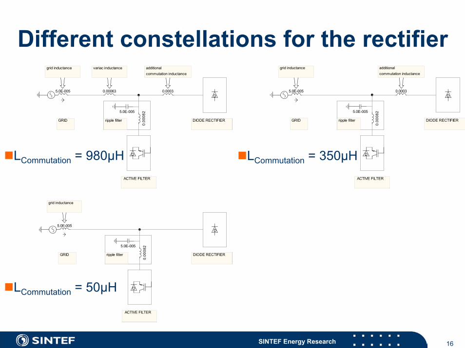
3.7 AC-side waveforms (active filter tasks for RL-DC-load at the rectifier) ........... 20 3.7.1 Active filtering for LG=650µH and LAC=300µH (file: ex04.psc) ......... 21 3.7.2 Active filtering for LG=50µH and LAC=300µH (file: ex05.psc) ........... 23 3.7.3 Active filtering for LG=50µH and LAC=0 (file: ex06.psc) .................... 24
3.8 Active filtering for a rectifier with RC-DC-load (file: ex07.psc) ....................... 25
4 EXPERIMENTAL SETUP OF THE SHUNT ACTIVE FILTER ................................. 28 4.1 The power grid .................................................................................................... 28 4.2 B6 diode rectifier load......................................................................................... 28
4.2.1 Inductive DC load ................................................................................. 28 4.2.2 Capacitive DC load ............................................................................... 31
4.3 The active filter ................................................................................................... 32 4.3.1 Control module ..................................................................................... 32 4.3.2 IGBT-converter..................................................................................... 33
5 CONTROL SOFTWARE ............................................................................................... 35 5.1 Interrupt structure................................................................................................ 35 5.2 Block diagram of the control system .................................................................. 36
12x127 AN 02.12.69
3
6 RESULTS AND MEASUREMENTS............................................................................ 52 6.1 Accrued problems ............................................................................................... 52
6.1.1 Oscillation of the filter capacitor with the grid inductance................... 52 6.1.2 Delayed current (Dead time between measurement and current output)54
6.2 Harmonic current and reactive power compensation for a diode rectifier.......... 56 6.2.1 230V over variac, additive commutation inductance ........................... 58 6.2.2 230V direct from the grid, additive commutation inductance .............. 62 6.2.3 230V direct from the grid, no additional inductance ............................ 66 6.2.4 Rectifier with capacitive DC-load ........................................................ 70
7 SUMMARY AND CONCLUSION ............................................................................... 74
9 APPENDIX A................................................................................................................. 78 9.1 Parameters used in the simulation model............................................................ 79 9.2 Calculation of specific parameters ...................................................................... 83
10 APPENDIX B ................................................................................................................. 84 10.1 Further calculations............................................................................................. 84 10.2 Used components ................................................................................................ 84
12x127 AN 02.12.69
1SINTEF Energy Research
”Power electronics and energy storage technologies for cost- and energy efficient power
systems”
SIP-strategic institute programme
AN 02.12.69 - Realisation of a 20kVA shunt active filter(Andre Buettner)
2SINTEF Energy Research
Why filter?
Problem:Insufficient power quality in low voltage AC-systems
Reasons:External disturbances (power outages, sags a.s.o.)Combined use of linear and non-linear loads (consumer of non-sinusoidal currents) causes current harmonics
3SINTEF Energy Research
Compensation for harmonic currents
Solution2:Active filter
Compensation for a selected or all harmonicsCompensation for reactive power is possible
Solution1:Passive harmonic filter
Compensation for a specific harmonicProblem: causes oscillation with the grid inductance
4SINTEF Energy Research
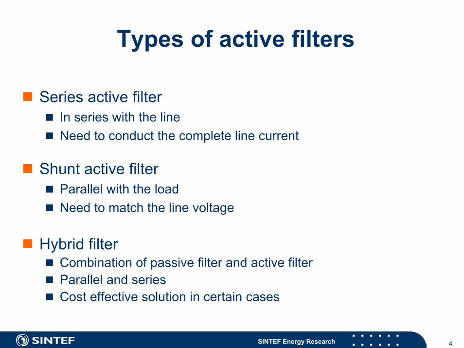
Types of active filters
Series active filterIn series with the lineNeed to conduct the complete line current
Shunt active filterParallel with the loadNeed to match the line voltage
Hybrid filterCombination of passive filter and active filterParallel and seriesCost effective solution in certain cases
5SINTEF Energy Research
Working mechanism for a shunt active filter
AC three-phasesource
Activefilter
iFilter
iMains iRectifier
iMeasure
Dioderectifier
6SINTEF Energy Research
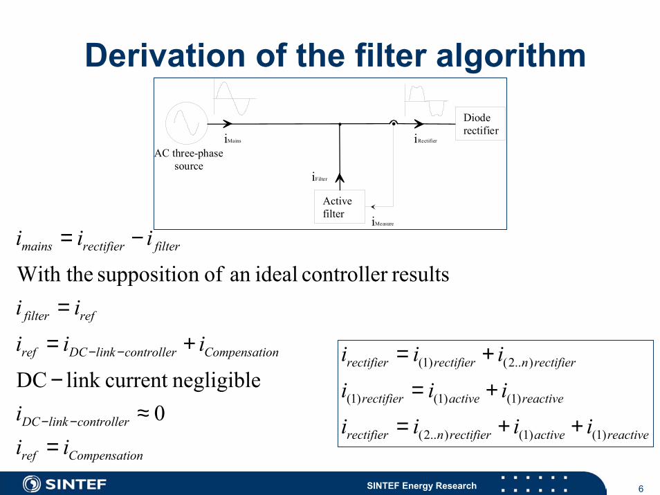
Derivation of the filter algorithm
onCompensatiref
controllerlinkDC
onCompensaticontrollerlinkDCref
reffilter
filterrectifiermains
iii
iiiii
iii
=≈
−
+=
=
−=
−−
−−
0negligiblecurrent link DC
results controller idealan ofn suppositio With the
reactiveactiverectifiernrectifier
reactiveactiverectifier
rectifiernrectifierrectifier
iiiiiiiiii
)1()1()..2(
)1()1()1(
)..2()1(
++=
+=
+=
AC three-phasesource
Activefilter
iFilter
iMains iRectifier
iMeasure
Dioderectifier
7SINTEF Energy Research
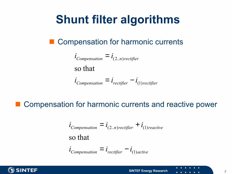
Shunt filter algorithms
Compensation for harmonic currents
rectifierrectifieronCompensati
rectifiernonCompensati
iii
ii
)1(
)..2(
thatso−=
=
Compensation for harmonic currents and reactive power
activerectifieronCompensati
reactiverectifiernonCompensati
iii
iii
)1(
)1()..2(
thatso−=
+=
8SINTEF Energy Research
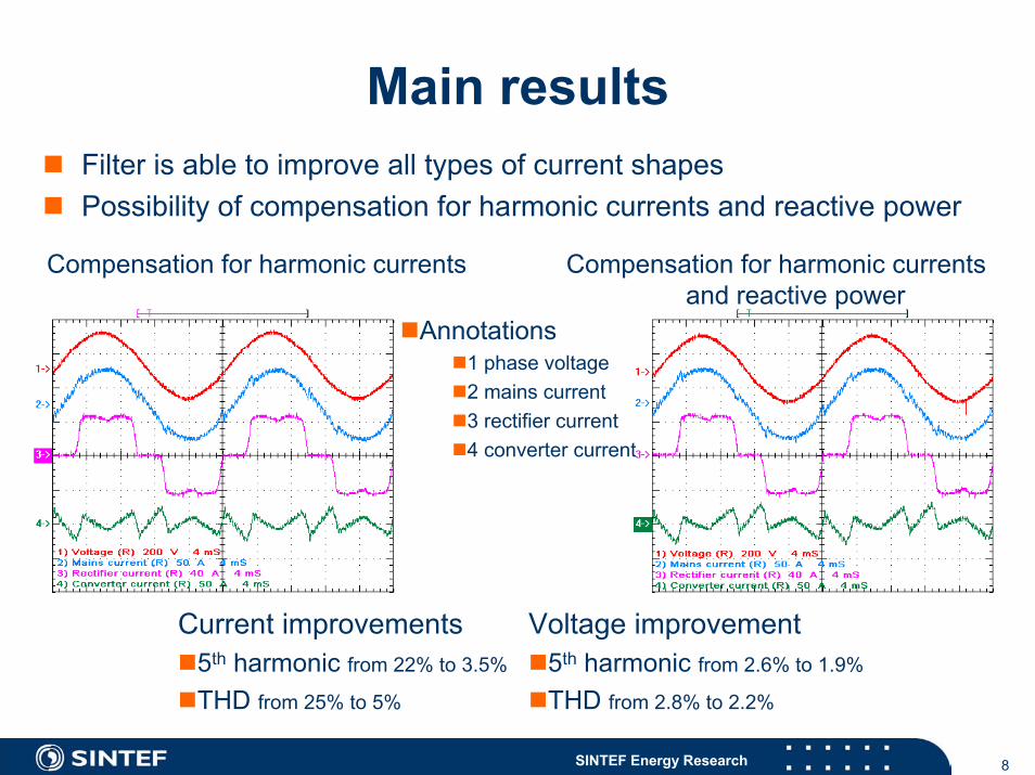
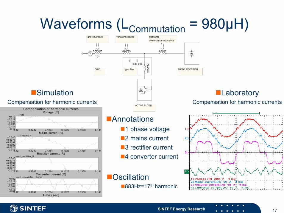
Main resultsFilter is able to improve all types of current shapesPossibility of compensation for harmonic currents and reactive power
Compensation for harmonic currents Compensation for harmonic currents and reactive power
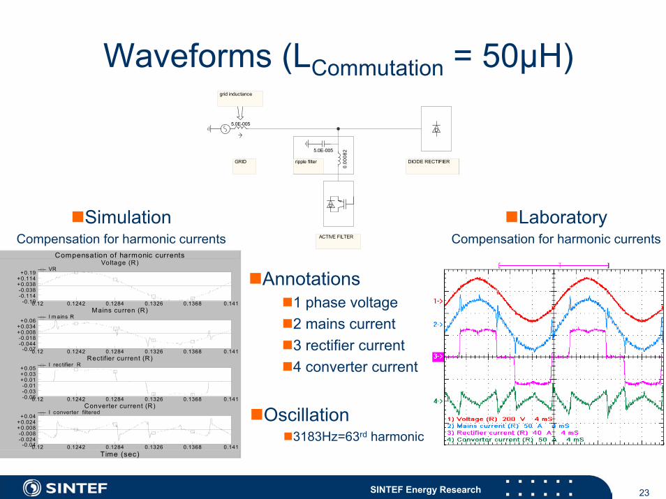
Annotations1 phase voltage2 mains current3 rectifier current4 converter current
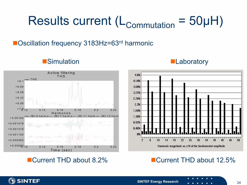
Current improvements5th harmonic from 22% to 3.5%
THD from 25% to 5%
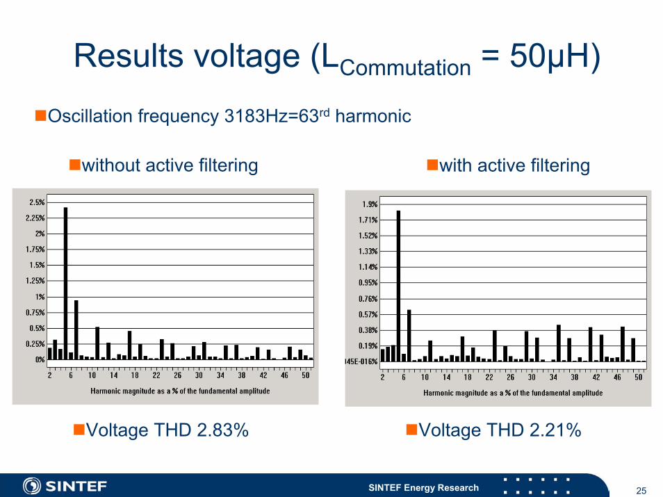
Voltage improvement5th harmonic from 2.6% to 1.9%
THD from 2.8% to 2.2%
9SINTEF Energy Research
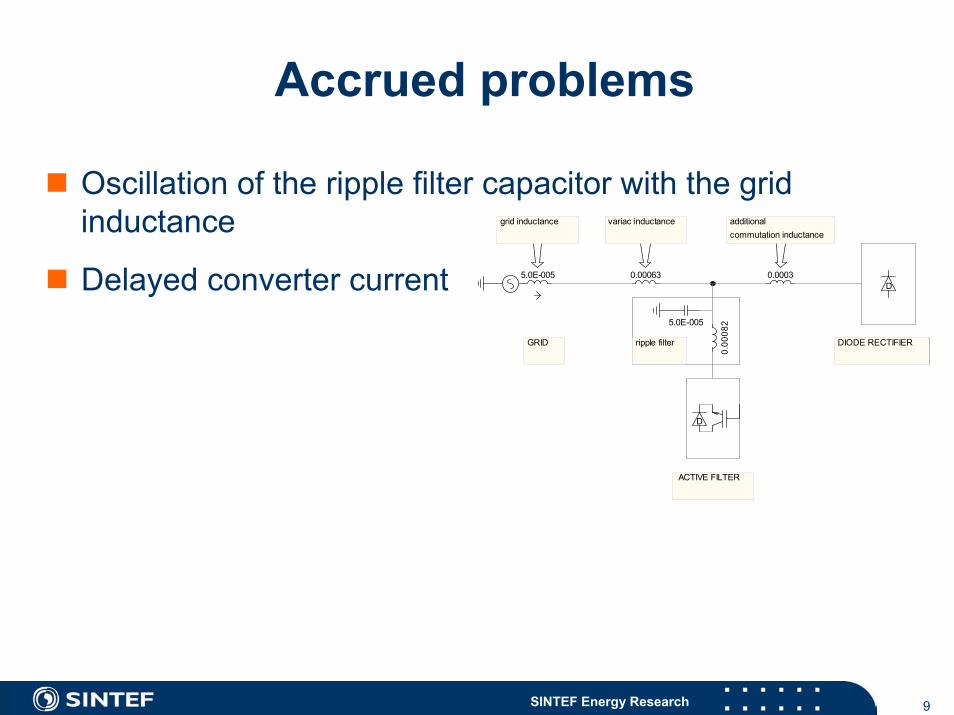
Accrued problems
Oscillation of the ripple filter capacitor with the grid inductance
D
D
grid inductance
5.0E-005
additionalcommutation inductance
GRID
0.0003
0.00
0825.0E-005
ripple filter
ACTIVE FILTER
variac inductance
0.00063
DIODE RECTIFIER
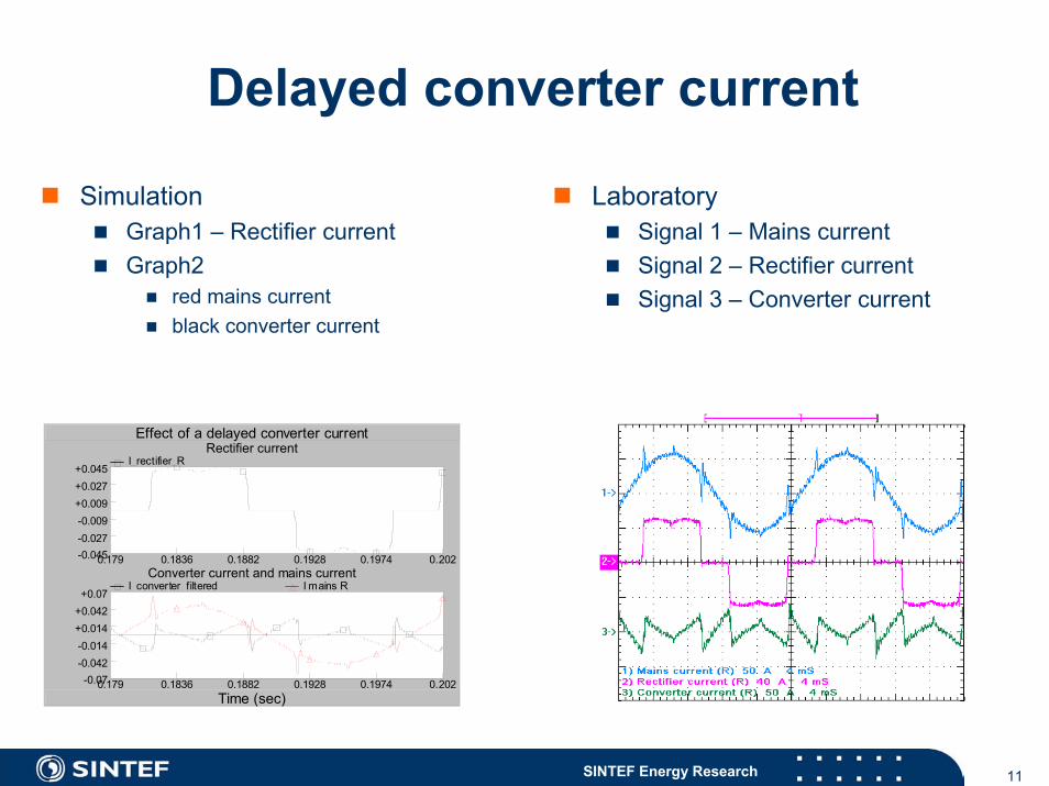
Delayed converter current
10SINTEF Energy Research
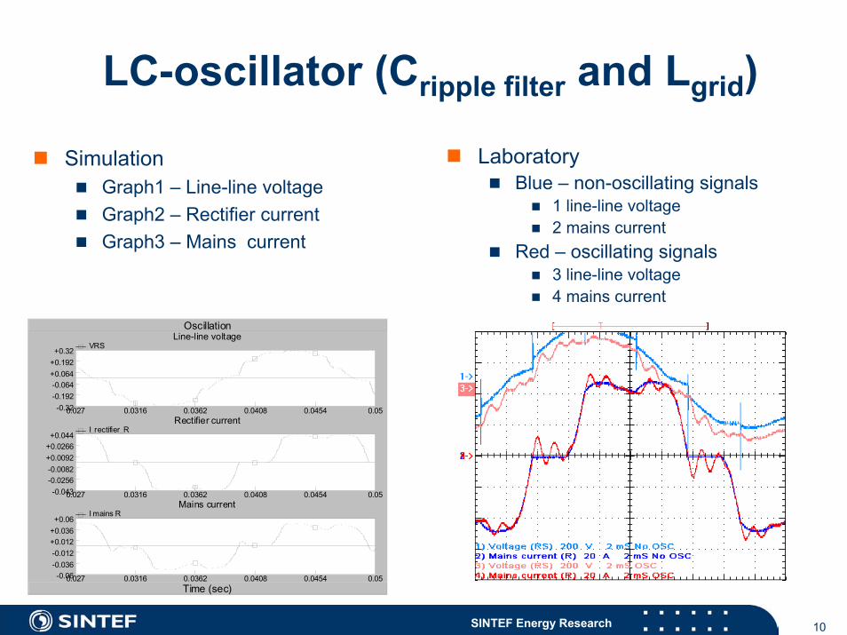
LC-oscillator (Cripple filter and Lgrid)
SimulationGraph1 – Line-line voltageGraph2 – Rectifier currentGraph3 – Mains current
LaboratoryBlue – non-oscillating signals
1 line-line voltage2 mains current
Red – oscillating signals3 line-line voltage4 mains current
delay between rectifier current measurement and output of the current reference
Current controller delaydelay between reference and output of the fire pulses
IGBT on delayTurn on turn off of the gate drivers (negligible small)
AnnotationsSignal1 – Rectifier currentSignal2 – Current referenceSignal3 – Converter current
13SINTEF Energy Research
Micro controller delaybetween current measurement and current reference output60µs - fastest interrupt repeating time
AnnotationsSignal1 – Rectifier currentSignal2 – Current reference
Improvementsfaster AD-converterDecrease number of channels in use
14SINTEF Energy Research
Current controller delaybetween current reference and output of the converter current0 to 150µs – depending on the reference frequencybandwidth problem
AnnotationsSignal1 – Current referenceSignal2 – Converter current
ImprovementsFaster current controllerDifferent typ of current controller
15SINTEF Energy Research
Diode rectifier with inductive DC-load
A
B
C
5.0E-005 0.00
127.
2
Line-line voltage
Rectifier current
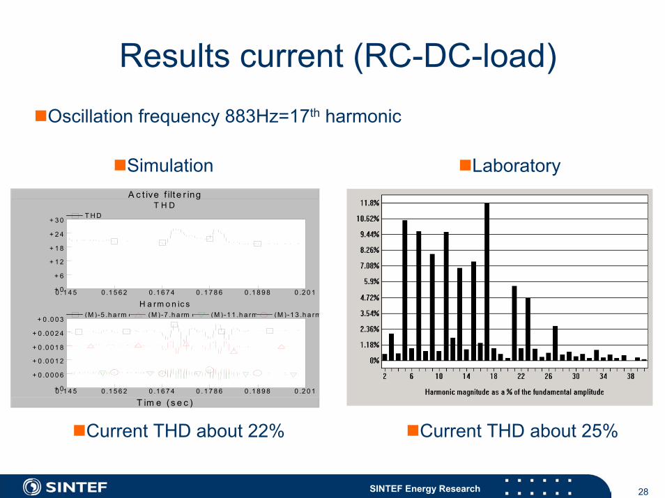
5th current harmonic 22%Current THD 25%-29% (Depending on the commutation)
+ 0 .0 0 3(M )-5 .h a rm o (M )-7 .h a rm o (M )-1 1 .h a rm (M )-1 3 .h a rm
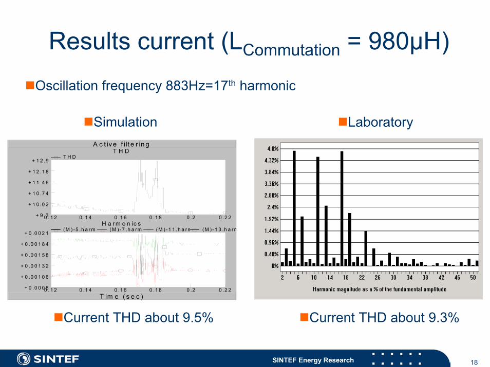
Current THD about 22% Current THD about 25%
29SINTEF Energy Research
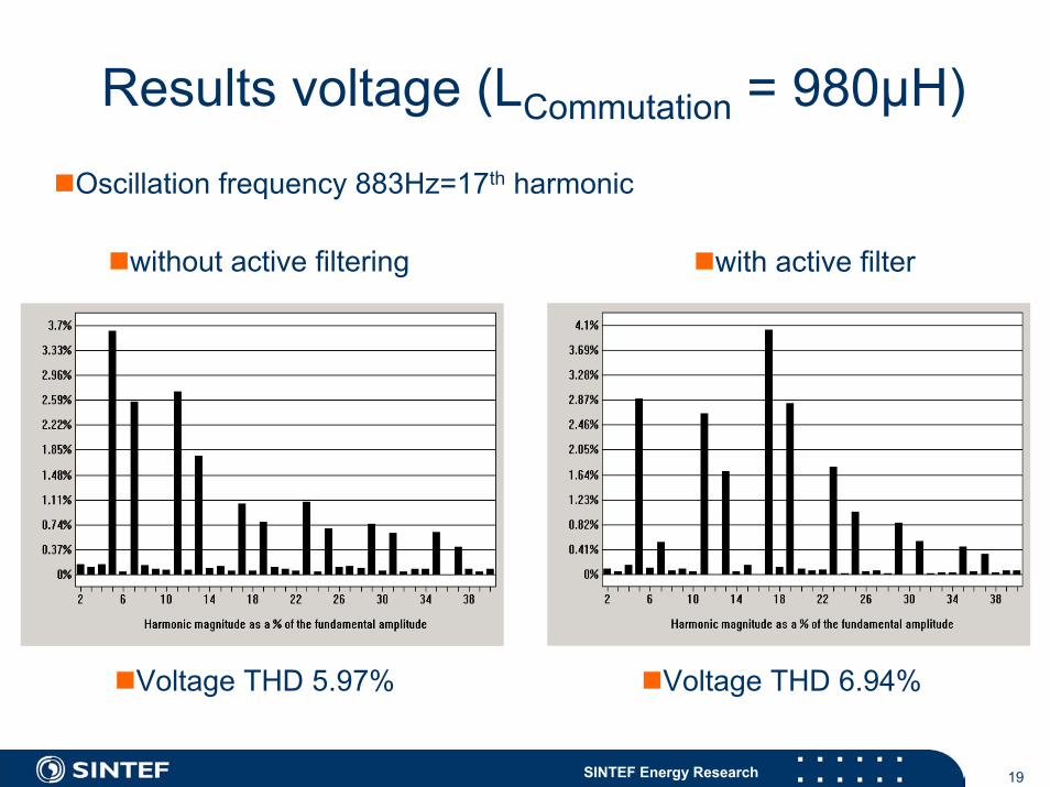
Results voltage (RC-DC-load)Oscillation frequency 883Hz=17th harmonic
without active filtering with active filtering
Voltage THD 5.4% Voltage THD 7.3%
30SINTEF Energy Research
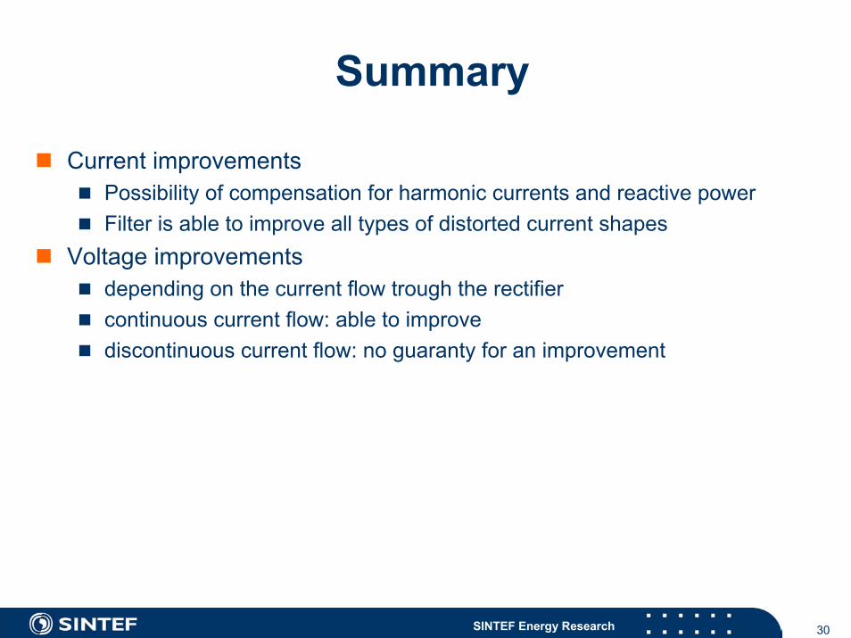
Summary
Current improvementsPossibility of compensation for harmonic currents and reactive powerFilter is able to improve all types of distorted current shapes
Voltage improvementsdepending on the current flow trough the rectifiercontinuous current flow: able to improvediscontinuous current flow: no guaranty for an improvement
31SINTEF Energy Research
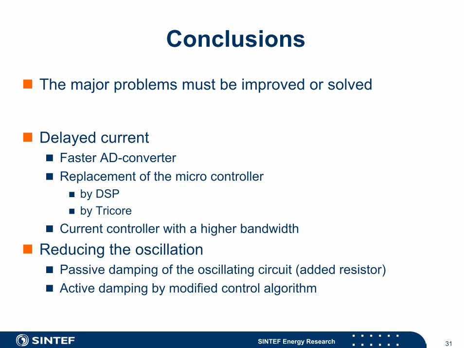
Conclusions
The major problems must be improved or solved
Delayed currentFaster AD-converterReplacement of the micro controller
by DSPby Tricore
Current controller with a higher bandwidthReducing the oscillation
Passive damping of the oscillating circuit (added resistor)Active damping by modified control algorithm


![Clergy Compensation Presentation.pptx [Read-Only] · 2017-11-07 · The compensation for whodoes it (Memo #4): ... counsel when setting up local church-sponsored benefit plans. Pensions](https://static.documents.pub/doc/80x56/5ec7e2f2545247384a4f30b5/clergy-compensation-read-only-2017-11-07-the-compensation-for-whodoes-it-memo.jpg)


