Page 1
1
EE141 – Fall 2005Lecture 7
Propagation Delay, Propagation Delay, Power DissipationPower Dissipation
EE141 2
Important!
Software Lab 3 this week
Enrollments increased to 86
Hw-3 due on Thursday 5pm• Check it out early (time to ask questions)
Page 2
2
EE141 3
Today’s Lecture
Inverter Performance
Power Dissipation
Review:
MOS Capacitances: MOS Capacitances: Dynamic BehaviorDynamic Behavior
Page 3
3
EE141 5
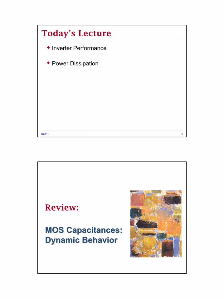
CGDCGS
CSB CDBCGB
(Miller)
Capacitive Device Model
= CGCS + CGSO = CGCD + CGDO
= CGCB= Cdiff
G
S D
B
= Cdiff
EE141 6
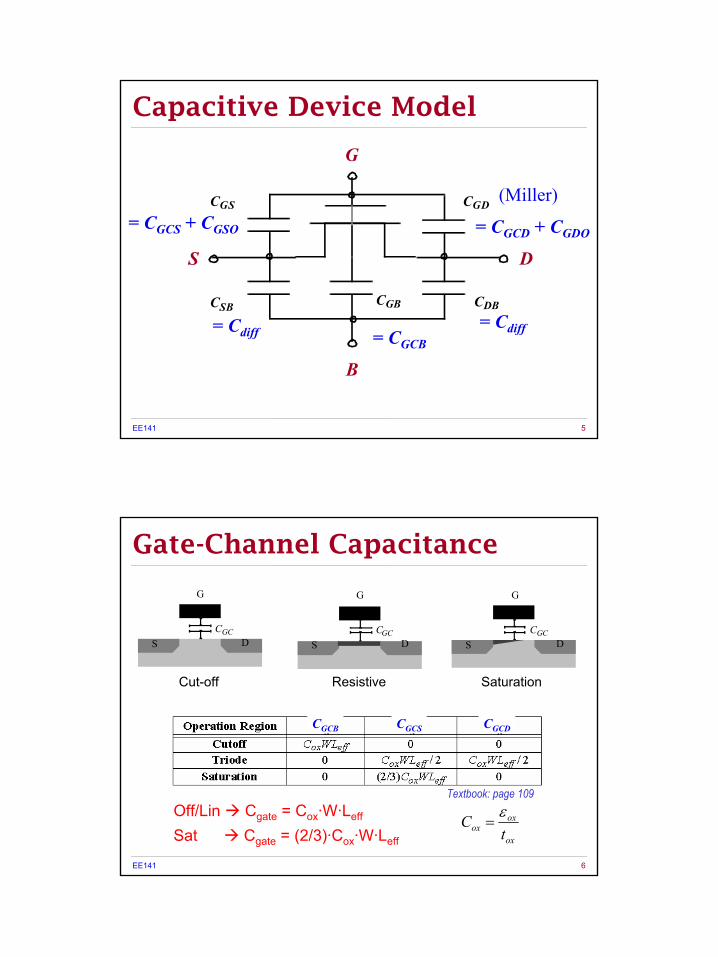
Gate-Channel Capacitance
S D
G
CGC
S D
G
CGCS D
G
CGC
Cut-off Resistive Saturation
Off/Lin Cgate = Cox·W·Leff
Textbook: page 109
CGCB CGCS CGCD
Sat Cgate = (2/3)·Cox·W·Leff ox
oxox t
C ε=
Page 4
4
EE141 7
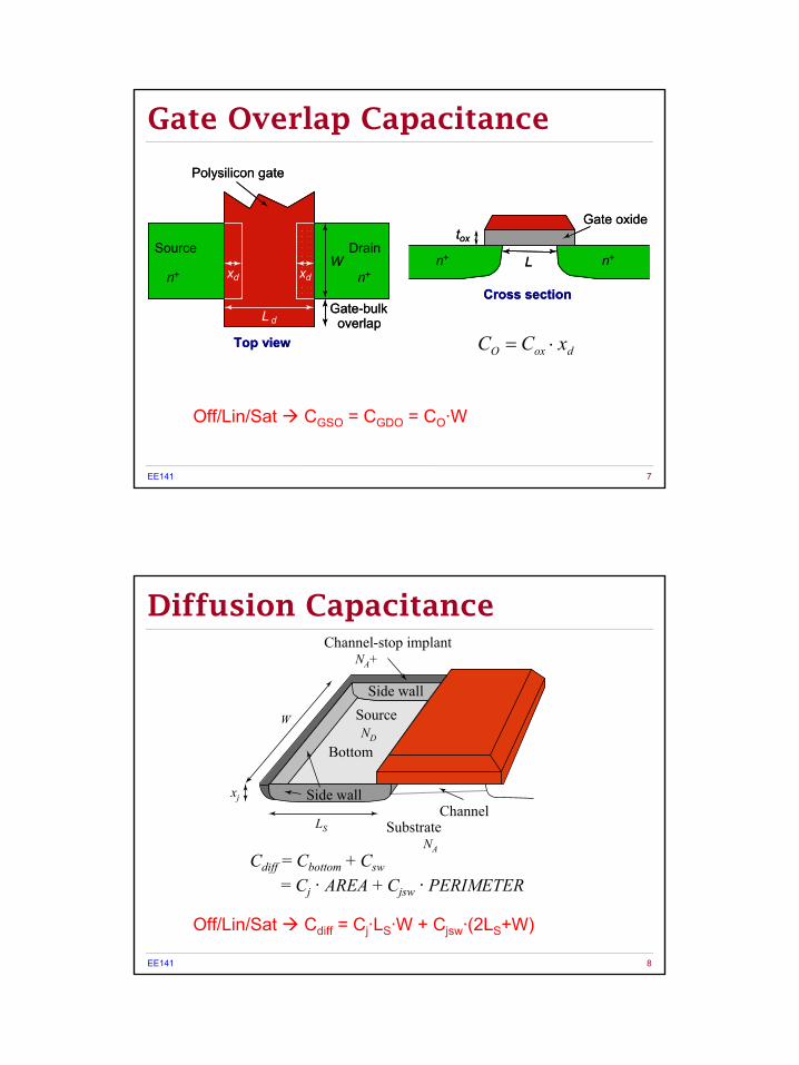
Gate Overlap Capacitance
doxO xCC ⋅=
xd xd
L d
Polysilicon gate
Top view
Gate-bulkoverlap
Source
n+
Drain
n+W
xd xd
L d
Polysilicon gate
Top view
Gate-bulkoverlap
Source
n+
Drain
n+W
Off/Lin/Sat CGSO = CGDO = CO·W
tox
n+ n+
Cross section
L
Gate oxidetox
n+ n+
Cross section
L
Gate oxide
EE141 8
Diffusion Capacitance
Bottom
Side wall
Side wallChannel
Source
Channel-stop implant
Substrate
W
NA+
NA
LS
ND
xj
Cdiff = Cbottom + Csw
= Cj · AREA + Cjsw · PERIMETER
Off/Lin/Sat Cdiff = Cj·LS·W + Cjsw·(2LS+W)
Page 5
5
EE141 9
Capacitive Device Model
Gate-Channel Capacitance• CGC = Cox·W·Leff (Off, Linear)• CGC = (2/3)·Cox·W·Leff (Saturation)
Gate Overlap Capacitance• CGSO = CGDO = CO·W (Always)
Junction/Diffusion Capacitance• Cdiff = Cj·LS·W + Cjsw·(2LS + W) (Always)
Zero-bias Cdiff > CgateMOS On Cdiff ≤ Cgate
EE141 10
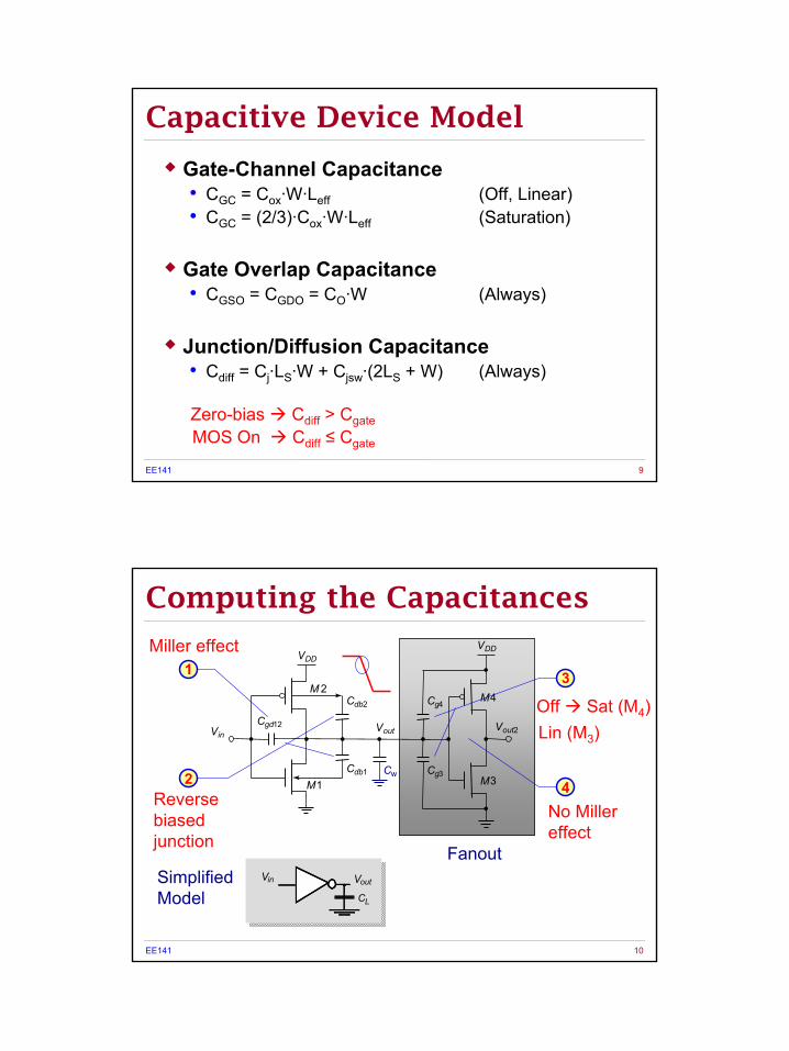
FanoutVoutVin
CL
SimplifiedModel
M3
M4
M1
M 2
Cw Cg3Cdb1
Cg4
Vout2
Cdb2
VDDVDD
Vin VoutCgd12
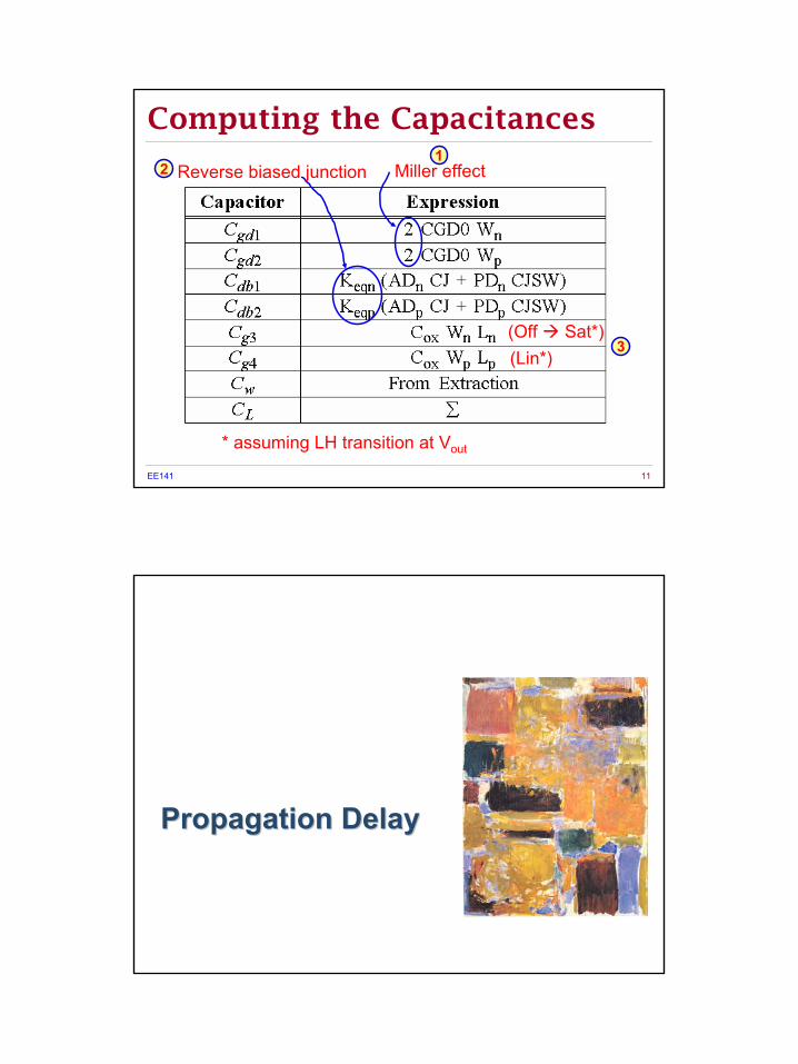
Computing the Capacitances
1
2
3
Miller effect
Reverse biased junction
Off Sat (M4)Lin (M3)
4No Miller effect
Page 6
6
EE141 11
Computing the Capacitances
Miller effect
(Off Sat*)(Lin*)
* assuming LH transition at Vout
Reverse biased junction1
2
3
Propagation DelayPropagation Delay
Page 7
7
EE141 13
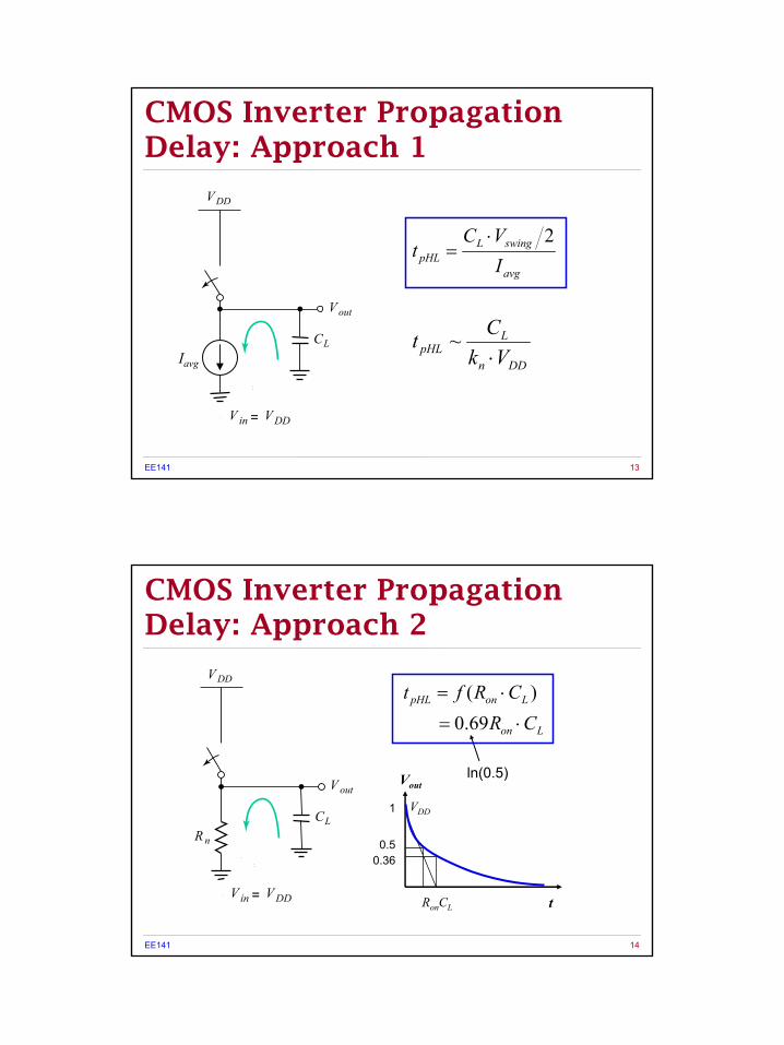
CMOS Inverter Propagation Delay: Approach 1
V out
Iavg
V DD
V in = V DD
CL
avg
swingLpHL I
VCt
2⋅=
DDn
LpHL Vk
Ct⋅
~
EE141 14
CMOS Inverter Propagation Delay: Approach 2
V out
R n
V DD
V in = V DD
CL
)( LonpHL CRft ⋅=
Lon CR ⋅= 69.0
0.360.5
1
RonCL t
Voutln(0.5)
VDD
Page 8
8
EE141 15
MOS Transistor as a SwitchTraversed path
ID
VDS
VDDVDD /2
VGS = VDD
Rmid
R0
∫∫ ⋅−
=⋅−
===
2
1
2
1
2
1 )()(1)(1))((
1212
t
t D
DSt
ton
t
ttoneq dttItV
ttdttR
tttRavgR
( ))()(21
21 tRtRR ononeq +⋅≈
VGS ≥ VT
S DRon
EE141 16
The Transistor as a Switch
VGS ≥ VT
S DRon
( ) ( )
⋅+⋅
+⋅+⋅
⋅=21
212
1
DDDSAT
DD
DDDSAT
DDeq VI
VVI
VRλλ
⋅⋅−⋅≈ DD
DSAT
DDeq V
IVR λ
651
43
ID
VDS
VDDVDD /2
VGS = VDD
Rmid
R0
( )021 RRR mideq +⋅=
Page 9
9
EE141 17
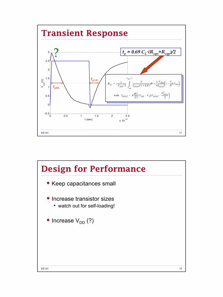
0 0.5 1 1.5 2 2.5
x 10-10
-0.5
0
0.5
1
1.5
2
2.5
3
t (sec)
Vou
t(V)
tp = 0.69 CL·(Reqn+Reqp)/2?
tpHL
tpLH
Transient Response
EE141 18
Design for Performance
Keep capacitances small
Increase transistor sizes• watch out for self-loading!
Increase VDD (?)
Page 10
10
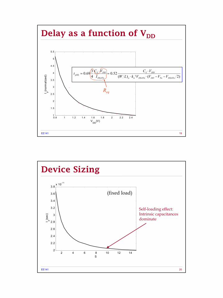
EE141 19
0.8 1 1.2 1.4 1.6 1.8 2 2.2 2.41
1.5
2
2.5
3
3.5
4
4.5
5
5.5
VDD
(V)
t p(nor
mal
ized
)
Delay as a function of VDD
)2(')(52.0
4369.0
DSATnTnDDDSATnnn
DDL
DSATn
DDLpHL VVVVkLW
VCI
VCt−−⋅⋅⋅
⋅=
⋅=
Req
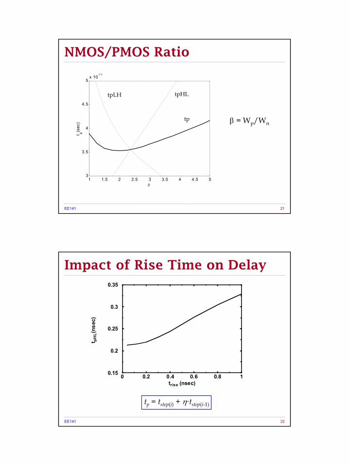
EE141 20
2 4 6 8 10 12 142
2.2
2.4
2.6
2.8
3
3.2
3.4
3.6
3.8x 10
-11
S
t p(sec
)
Device Sizing
(fixed load)
Self-loading effect:Intrinsic capacitancesdominate
Page 11
11
EE141 21
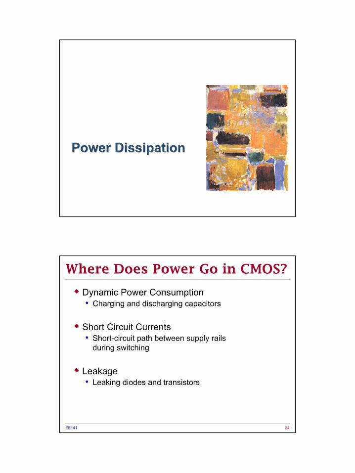
1 1.5 2 2.5 3 3.5 4 4.5 53
3.5
4
4.5
5x 10
-11
β
t p(sec
)
NMOS/PMOS Ratio
tpLH tpHL
tp β = Wp/Wn
EE141 22
t pH
L(ns
ec)
0.35
0.3
0.25
0.2
0.15
trise (nsec)10.80.60.40.20
Impact of Rise Time on Delay
tp = tstep(i) + η·tstep(i-1)
Page 12
12
Power DissipationPower Dissipation
EE141 24
Where Does Power Go in CMOS?
Dynamic Power Consumption• Charging and discharging capacitors
Short Circuit Currents• Short-circuit path between supply rails
during switching
Leakage• Leaking diodes and transistors
Page 13
13
EE141 25
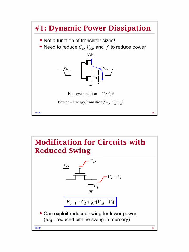
#1: Dynamic Power Dissipation
Vin Vout
CL
Vdd
Not a function of transistor sizes!Need to reduce CL, Vdd, and f to reduce power
Energy/transition = CL·Vdd2
Power = Energy/transition·f = f·CL·Vdd2
EE141 26
Modification for Circuits with Reduced Swing
Can exploit reduced swing for lower power(e.g., reduced bit-line swing in memory)
E0→1 = CL·Vdd·(Vdd – Vt)
CL
Vdd
Vdd – Vt
Vdd
Page 14
14
EE141 27
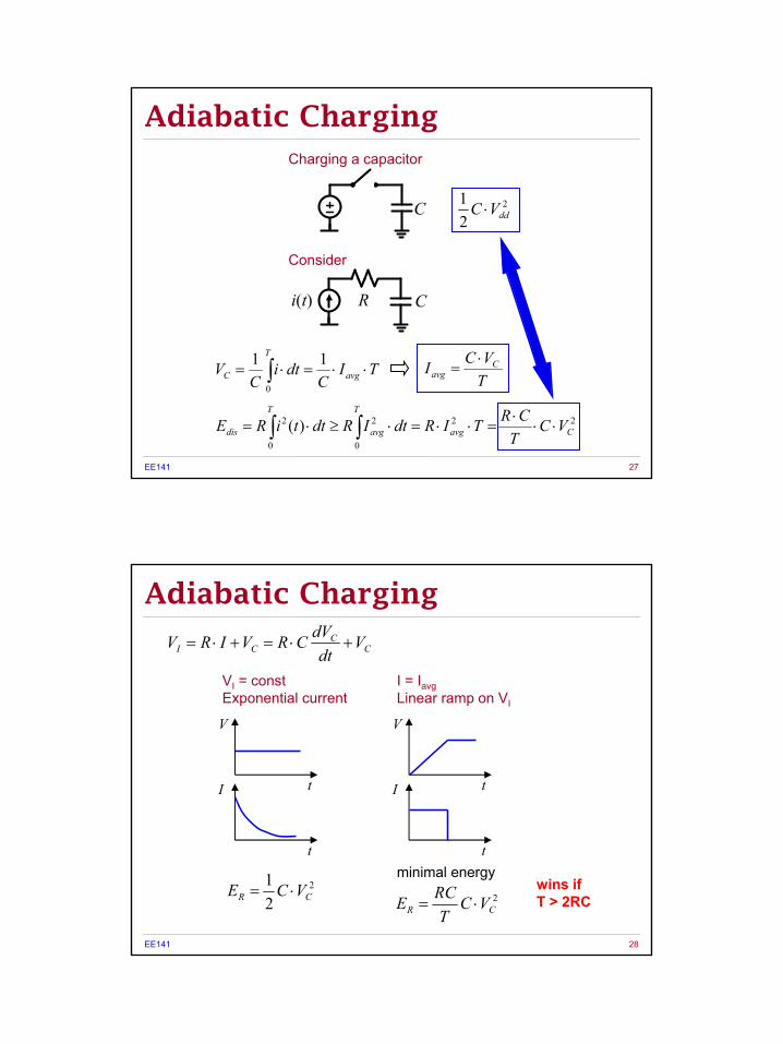
Adiabatic Charging
i(t) R C
C
Consider
Charging a capacitor
∫ ⋅⋅=⋅=T
avgC TIC
dtiC
V0
11
2
21
ddVC ⋅
TVCI C
avg⋅
=
2
0
2
0
22 )( C
T
avg
T
avgdis VCT
CRTIRdtIRdttiRE ⋅⋅⋅
=⋅⋅=⋅≥⋅= ∫ ∫
EE141 28
Adiabatic Charging
CC
CI Vdt
dVCRVIRV +⋅=+⋅=
VI = constExponential current
2
21
CR VCE ⋅= 2CR VC
TRCE ⋅=
I = IavgLinear ramp on VI
minimal energywins if T > 2RC
t
I
t
It
V
t
V
Page 15
15
EE141 29
Node Transition Activity and Power
Consider switching a CMOS gate for N clock cycles
EN = CL·Vdd2·n(N)
EN: the energy consumed for N clock cyclesn(N): the number of 0→1 transitions in N clock cycles
clkddLNclkN
Navg fVCNNnf
NEP ⋅⋅⋅
=⋅=
∞→∞→
2)(limlim
NNn
N
)(lim10 ∞→→ =α
Pavg = α0→1·CL·Vdd2·fclk
EE141 30
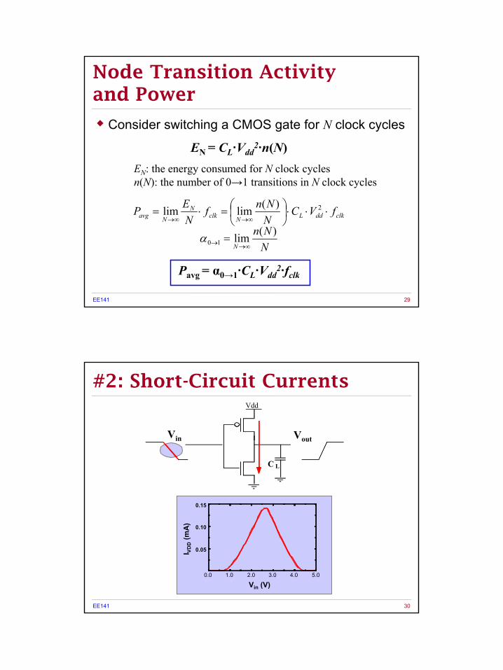
#2: Short-Circuit Currents
Vin Vout
C L
Vdd
0.15
0.10
0.05
5.04.03.02.01.00.0
I VD
D(m
A)
Vin (V)
Page 16
16
EE141 31
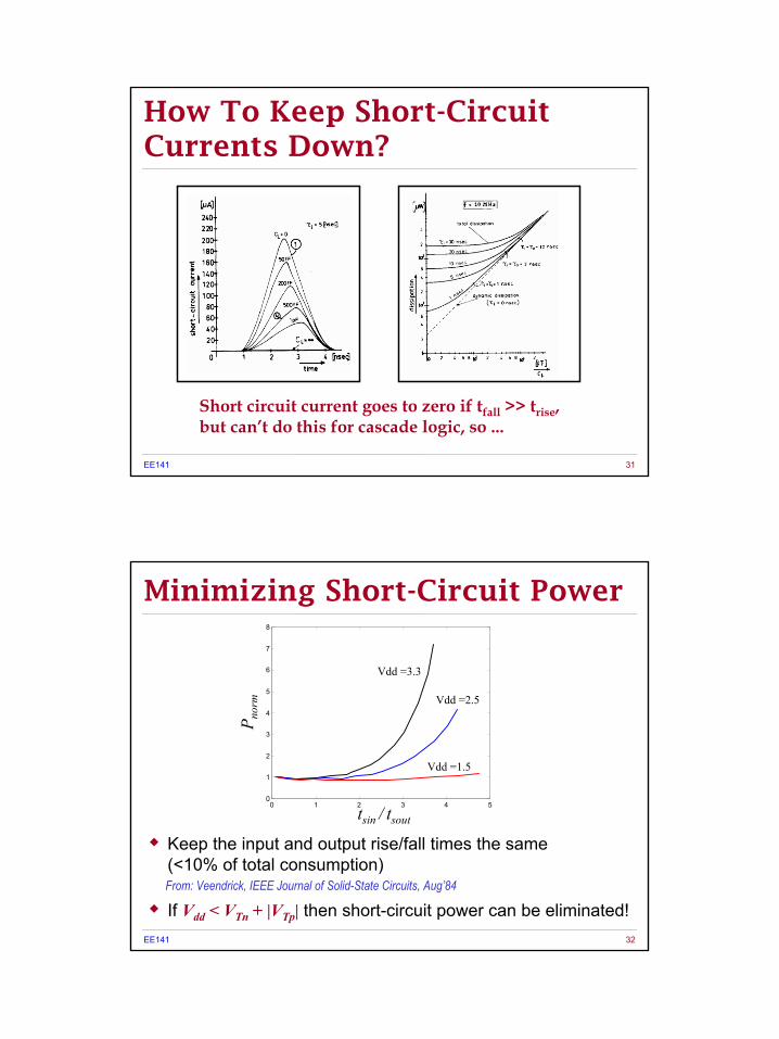
Short circuit current goes to zero if tfall >> trise,but can’t do this for cascade logic, so ...
How To Keep Short-Circuit Currents Down?
EE141 32
0 1 2 3 4 50
1
2
3
4
5
6
7
8
Vdd =1.5
Vdd =2.5
Vdd =3.3
Minimizing Short-Circuit Power
Keep the input and output rise/fall times the same (<10% of total consumption)
If Vdd < VTn + |VTp| then short-circuit power can be eliminated!From: Veendrick, IEEE Journal of Solid-State Circuits, Aug’84
tsin / tsout
P nor
m
Page 17
17
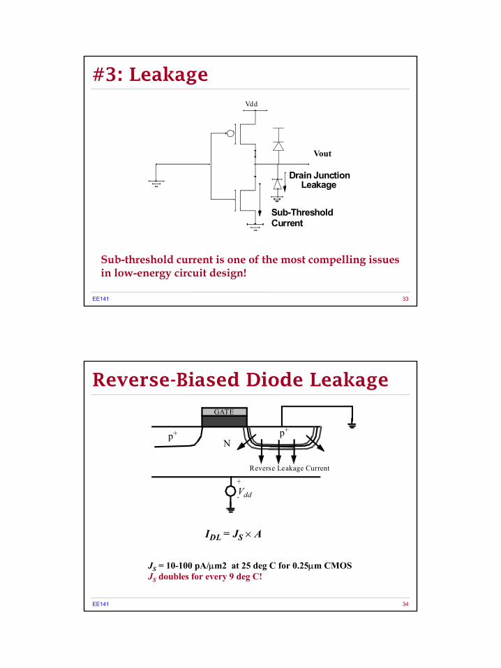
EE141 33
Vout
Vdd
Sub-ThresholdCurrent
Drain JunctionLeakage
Sub-threshold current is one of the most compelling issuesin low-energy circuit design!
#3: Leakage
EE141 34
Np+ p+
Reverse Leakage Current
+
-Vdd
GATE
IDL = JS × A
JS = 10-100 pA/µm2 at 25 deg C for 0.25µm CMOSJS doubles for every 9 deg C!
Reverse-Biased Diode Leakage
Page 18
18
EE141 35
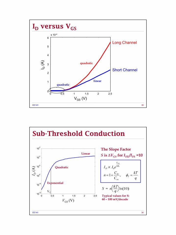
ID versus VGS
0 0.5 1 1.5 2 2.50
1
2
4
5
6x 10⁻⁴
Long Channel
Short Channel
quadraticlinear
quadratic
VGS (V)
I D(A
)
3
EE141 36
Sub-Threshold Conduction
Typical values for S:60 – 100 mV/decade
The Slope FactorS is ∆VGS for ID2 /ID1 =10
0 0.5 1 1.5 2 2.510
-12
10-10
10-8
10-6
10-4
10-2
VT
Linear
Exponential
Quadratic
VGS (V)
I D(A
)
qkT
CCn
eII
Tox
D
nV
DT
GS
=+=
∝
φ
φ
,1
0
Page 19
19
EE141 37
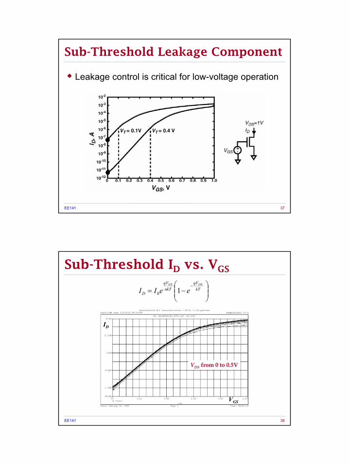
Sub-Threshold Leakage Component
Leakage control is critical for low-voltage operation
EE141 38
VDS from 0 to 0.5V
−=
−kT
qVnkT
qV
D
DSGS
eeII 10
Sub-Threshold ID vs. VGS
ID
VGS
Page 20
20
EE141 39
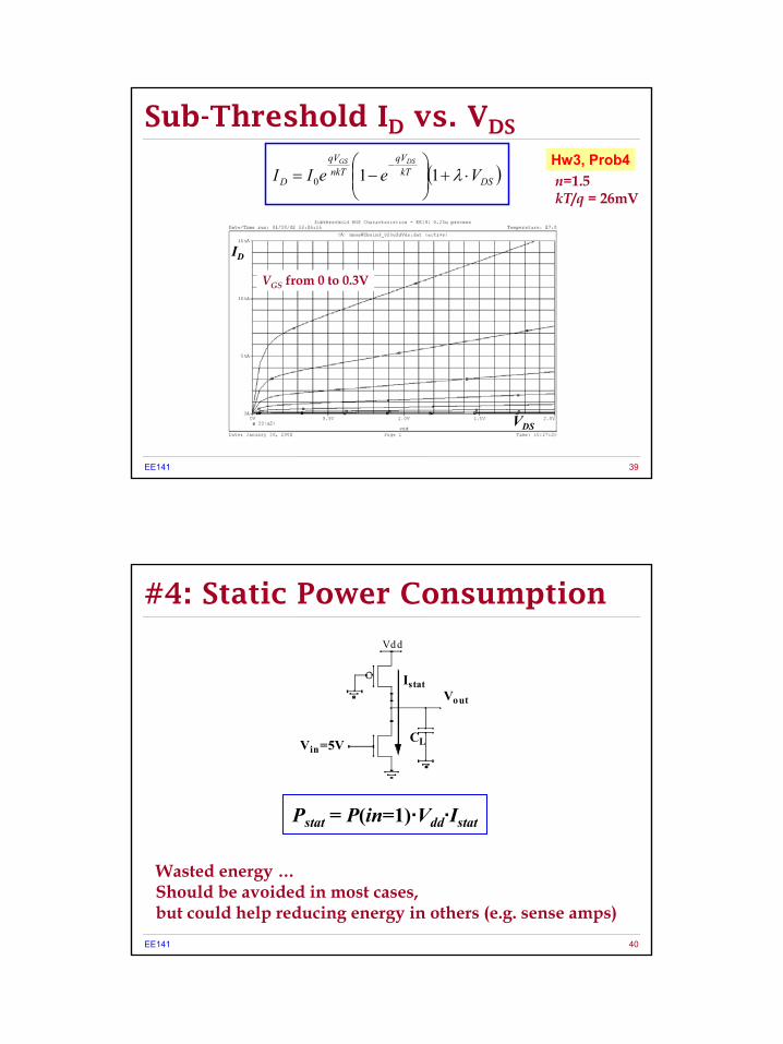
Sub-Threshold ID vs. VDS
( )DSkT
qVnkT
qV
D VeeIIDSGS
⋅+
−=
−λ110
VGS from 0 to 0.3V
ID
VDS
Hw3, Prob4n=1.5kT/q = 26mV
EE141 40
Vin=5V
Vout
CL
Vdd
Istat
Wasted energy …Should be avoided in most cases,but could help reducing energy in others (e.g. sense amps)
#4: Static Power Consumption
Pstat = P(in=1)·Vdd·Istat
Page 21
21
EE141 41
Prime choice: Reduce voltage!• Recent years have seen an acceleration in
supply voltage reduction• Design at very low voltages still open question
(0.6 … 0.9 V by 2010!)
Reduce switching activity
Reduce physical capacitance
Principles for Power Reduction
EE141 42
Threshold Variations
Sub-threshold Conduction
Parasitic Resistances
The Sub-Micron MOS Transistor
Page 22
22
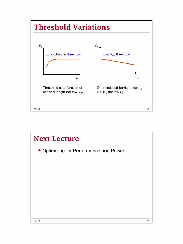
EE141 43
VT
L
Long-channel threshold
Threshold as a function ofchannel length (for low VDS)
VDS
VT
Threshold Variations
Low VDS threshold
Drain induced barrier lowering (DIBL) (for low L)
EE141 44
Next Lecture
Optimizing for Performance and Power


![lecture16-IP-switching...What do we know so far [1] … • Network performance metrics • Transmission delay, propagation delay, queueing delay, bandwidth • Sharing networks •](https://static.documents.pub/doc/80x56/5e9e91272561997647659170/lecture16-ip-switching-what-do-we-know-so-far-1-a-network-performance-metrics.jpg)


