This article was downloaded by: [Dalhousie University] On: 13 November 2013, At: 00:10 Publisher: Taylor & Francis Informa Ltd Registered in England and Wales Registered Number: 1072954 Registered office: Mortimer House, 37-41 Mortimer Street, London W1T 3JH, UK Journal of Electromagnetic Waves and Applications Publication details, including instructions for authors and subscription information: http://www.tandfonline.com/loi/tewa20 Properties of the defect modes in 1D lossy photonic crystals containing two types of negative-index-material defects Alireza Aghajamali ab , Mozhgan Hayati c , Chien-Jang Wu d & Mahmood Barati a a Department of Physics, Science and Research Branch, Islamic Azad University, Fars, 73715-181, Iran. b Young Researchers Club, Science and Research Branch, Islamic Azad University, Fars, Iran. c Department of Physics, Marvdasht Branch, Islamic Azad University, Marvdasht, Iran. d Institute of Electro-Optical Science and Technology, National Taiwan Normal University, Taipei, 116, Taiwan, ROC. Published online: 08 Oct 2013. To cite this article: Alireza Aghajamali, Mozhgan Hayati, Chien-Jang Wu & Mahmood Barati (2013) Properties of the defect modes in 1D lossy photonic crystals containing two types of negative- index-material defects, Journal of Electromagnetic Waves and Applications, 27:18, 2317-2329, DOI: 10.1080/09205071.2013.843475 To link to this article: http://dx.doi.org/10.1080/09205071.2013.843475 PLEASE SCROLL DOWN FOR ARTICLE Taylor & Francis makes every effort to ensure the accuracy of all the information (the “Content”) contained in the publications on our platform. However, Taylor & Francis, our agents, and our licensors make no representations or warranties whatsoever as to the accuracy, completeness, or suitability for any purpose of the Content. Any opinions and views expressed in this publication are the opinions and views of the authors, and are not the views of or endorsed by Taylor & Francis. The accuracy of the Content should not be relied upon and should be independently verified with primary sources of information. Taylor and Francis shall not be liable for any losses, actions, claims, proceedings, demands, costs, expenses, damages, and other liabilities whatsoever or
Transcript
This article was downloaded by: [Dalhousie University]On: 13 November 2013, At: 00:10Publisher: Taylor & FrancisInforma Ltd Registered in England and Wales Registered Number: 1072954 Registeredoffice: Mortimer House, 37-41 Mortimer Street, London W1T 3JH, UK
Journal of Electromagnetic Waves andApplicationsPublication details, including instructions for authors andsubscription information:http://www.tandfonline.com/loi/tewa20
Properties of the defect modes in1D lossy photonic crystals containingtwo types of negative-index-materialdefectsAlireza Aghajamaliab, Mozhgan Hayatic, Chien-Jang Wud &Mahmood Baratiaa Department of Physics, Science and Research Branch, IslamicAzad University, Fars, 73715-181, Iran.b Young Researchers Club, Science and Research Branch, IslamicAzad University, Fars, Iran.c Department of Physics, Marvdasht Branch, Islamic AzadUniversity, Marvdasht, Iran.d Institute of Electro-Optical Science and Technology, NationalTaiwan Normal University, Taipei, 116, Taiwan, ROC.Published online: 08 Oct 2013.
To cite this article: Alireza Aghajamali, Mozhgan Hayati, Chien-Jang Wu & Mahmood Barati (2013)Properties of the defect modes in 1D lossy photonic crystals containing two types of negative-index-material defects, Journal of Electromagnetic Waves and Applications, 27:18, 2317-2329, DOI:10.1080/09205071.2013.843475
To link to this article: http://dx.doi.org/10.1080/09205071.2013.843475
PLEASE SCROLL DOWN FOR ARTICLE
Taylor & Francis makes every effort to ensure the accuracy of all the information (the“Content”) contained in the publications on our platform. However, Taylor & Francis,our agents, and our licensors make no representations or warranties whatsoever as tothe accuracy, completeness, or suitability for any purpose of the Content. Any opinionsand views expressed in this publication are the opinions and views of the authors,and are not the views of or endorsed by Taylor & Francis. The accuracy of the Contentshould not be relied upon and should be independently verified with primary sourcesof information. Taylor and Francis shall not be liable for any losses, actions, claims,proceedings, demands, costs, expenses, damages, and other liabilities whatsoever or
howsoever caused arising directly or indirectly in connection with, in relation to or arisingout of the use of the Content.
This article may be used for research, teaching, and private study purposes. Anysubstantial or systematic reproduction, redistribution, reselling, loan, sub-licensing,systematic supply, or distribution in any form to anyone is expressly forbidden. Terms &Conditions of access and use can be found at http://www.tandfonline.com/page/terms-and-conditions
Properties of the defect modes in 1D lossy photonic crystalscontaining two types of negative-index-material defects
Alireza Aghajamalia,b*, Mozhgan Hayatic, Chien-Jang Wud and Mahmood Baratia
aDepartment of Physics, Science and Research Branch, Islamic Azad University, Fars, Iran;bYoung Researchers Club, Science and Research Branch, Islamic Azad University, Fars, Iran;
cDepartment of Physics, Marvdasht Branch, Islamic Azad University, Marvdasht, Iran; dInstituteof Electro-Optical Science and Technology, National Taiwan Normal University, Taipei 116,
Taiwan, ROC
(Received 7 June 2013; accepted 6 September 2013)
In this paper, the characteristic matrix method is employed to theoreticallyinvestigate the propagation of electromagnetic waves through one-dimensionaldefective lossy photonic crystals composed of negative-index materials (NIMs) andpositive-index materials. We consider symmetric and asymmetric geometric struc-tures with two different types of NIM defect layers at the center of the structure.The effects of polarization and the angle of incidence on the defect modes in thetransmission spectra of both the structures are investigated. The results show that thenumber of the defect modes within the photonic band gap depends on the type ofthe NIM defect layer and is independent of the geometrical structure. Moreover, it isshown that the defect mode frequency increases as the angle of incidence increases.This property is also independent of the geometry of the structure. The results canlead to designing new types of narrowband and multichannel transmission filters.
Keywords: photonic crystal; defect mode; loss factor; negative-index material;photonic band gap
1. Introduction
Over the past two and half decades, a new class of material called photonic crystals(PCs) has emerged. The PCs originate from the theoretical work of Yablonovitch andJohn’s experimental work, which were published almost simultaneously in 1987.[1,2]The PCs are artificial dielectric or metallic structures in which the refractive indexchanges periodically in space. This kind of periodic structure affects the propagation ofelectromagnetic waves in the similar way as the periodic potential in a semiconductorcrystal affects the electron motion by defining allowed and forbidden electronic energybands. Whether or not photons propagate through PC structures depends on their fre-quency. Frequencies that are allowed to travel are known as modes, and groups ofallowed modes form bands. Disallowed bands of frequencies are called photonic bandgaps (PBGs).[3,4] These PBGs are also called Bragg gaps because they originate fromBragg scattering in the periodic structure. The properties of the PBGs inone-dimensional (1D) PCs have been proven to play an important role in some potential
Journal of Electromagnetic Waves and Applications, 2013Vol. 27, No. 18, 2317–2329, http://dx.doi.org/10.1080/09205071.2013.843475
� 2013 Taylor & Francis
Dow
nloa
ded
by [
Dal
hous
ie U
nive
rsity
] at
00:
10 1
3 N
ovem
ber
2013
applications such as photonic devices, optical filters, resonance cavities, laser applica-tions, high reflecting omnidirectional mirrors, and the optoelectronic circuits.[5–7]
By breaking the periodicity of the conventional PC structure, we will have a defec-tive crystal. This can be performed by changing physical parameters, such as changingthe thickness of one of the layers, adding another medium to the structure, or removinga layer from PCs.[8–10] By introducing a layer with different optical properties, local-ized defect modes, which are also called resonant transmission peaks, can be generatedwithin the PBG due to the change of the interference behavior of light,[10,11] verysimilar to the defect states that are generated in the forbidden band of doped semicon-ductors. Upon prediction of the existence of materials with negative refractive index(NRI) in 1968 by Veselago,[12] such materials, which have negative permittivity andpermeability simultaneously, have received extensive attention for their very unusualelectromagnetic properties. Negative refractive index materials, or simply negative-indexmaterials (NIMs), are now also known as metamaterials. Recently, with the possibilityof producing metamaterials, PCs with metamaterials called metamaterial photoniccrystals (MetaPCs) have been made.
In several papers, the properties of the defect modes in different 1D conventionalPC and 1D MetaPC structures have been investigated by introducing positive or nega-tive indices defects.[13–33] Following the interesting report by Wu et al. [19] on theproperties of the defect modes in 1D PCs with symmetric and asymmetric geometricstructures, here we investigate the properties of the defect modes in the transmissionspectra of 1D defective symmetric and asymmetric lossy MetaPCs, which are composedof negative refractive index material defect layer at the center of the crystal. The outlineof this paper is as follows. In Section 2, two geometric MetaPC structures, the permit-tivity and permeability of two types of NIMs, and also the characteristic matrix methodand its formulation are presented. The numerical results and discussions are given inSection 3, and the conclusion is presented in Section 4.
2. MetaPC structure and characteristic matrix method
The 1D defective MetaPCs, which are constituted by alternative layers of NIM andpositive-index material (PIM), under study with asymmetric and symmetric structures inair with a defect layer at the center of the structures are shown in Figure 1(a) and 1(b),respectively, where NIMs are dispersive and dissipative. We assume that the layers Aand C (defect layer) are NIMs, and layer B is a PIM. N is the number of the latticeperiod, and also di, ei, and li (i=A, B, C) are thickness, permittivity, and permeabilityof the layers, respectively.
The calculations are performed using the characteristic matrix method,[34] which isthe most effective technique to analyze the transmission properties of PCs. The charac-teristic matrices for asymmetric (AB)N/2C (AB)N/2, and symmetric (AB)N/2C (BA)N/2
structures, respectively, are given by: M ½d� ¼ ðMAMBÞN=2MCðMAMBÞN=2 and
M ½d� ¼ ðMAMBÞN=2MCðMBMAÞN=2; where MA, MB and MC are the characteristicmatrices of layers A, B, and C. The characteristic matrix Mi for TE wave is given by[34]:
Mi ¼ cos ci�ipisin ci
�ipi sin ci cos ci
� �; ð1Þ
2318 A. Aghajamali et al.
Dow
nloa
ded
by [
Dal
hous
ie U
nive
rsity
] at
00:
10 1
3 N
ovem
ber
2013
where ci ¼ ðx=cÞnidi cos hi, c is the speed of light in vacuum, hi is the ray angle inside
layer i with a refractive index ni, pi ¼ffiffiffiffiffiffiffiffiffiffiei=li
in which n0 is the refractive index of the environment wherein the incidence wave tendsto enter the structure. The refractive index is given as ni ¼ � ffiffiffiffiffiffiffi
eilip
,[28,35] where thepositive and the negative signs are assigned for the PIM and NIM layers, respectively.
The final characteristic matrix for an N period structure is given by:
½MðdÞ�N ¼YNi¼1
Mi � m11 m12
m21 m22
� �; ð2Þ
where mij ði; j ¼ 1; 2Þ are the matrix elements of ½MðdÞ�N . The transmission coefficientof the multilayer is calculated by:
t ¼ 2p0ðm11 þ m12psÞp0 þ ðm21 þ m22psÞ : ð3Þ
In this equation, p0 ¼ n0 cos h0 and ps ¼ ns cos hs, with ns being the refractive indexof the environment where the wave leaves the crystal with angle hs. The transmissivity
of the multilayer is given by T ¼ ðps=p0Þjtj2. The transmissivity of the multilayer for
TM wave can be obtained by using the replacements of pi ¼ffiffiffiffiffiffiffiffiffiffili=ei
pcos hi,
p0 ¼ cos h0=n0, and ps ¼ cos hs=ns.As mentioned before, our study is based on two different types of NIMs. The
permittivity and permeability of type-I NIM layer with a negative refracting index inthe microwave region are complex and are defined as,[36,37]
eð f Þ ¼ 1þ 52
0:92 � f 2 � if cþ 102
11:52 � f 2 � if cð4Þ
Figure 1. Schematic diagrams of 1D defective MetaPCs embedded in air, with a defect layer,(a) asymmetric structure, (b) symmetric structure, where layers A and C are NIMs and layer B isPIM. The number of the periods is N and the incidence angle is h0.
Journal of Electromagnetic Waves and Applications 2319
Dow
nloa
ded
by [
Dal
hous
ie U
nive
rsity
] at
00:
10 1
3 N
ovem
ber
2013
lð f Þ ¼ 1þ 32
0:9022 � f 2 � if cð5Þ
where f and c are frequency and damping frequency in GHz, respectively. Asmentioned in [37], for f\3:13 GHz, the real parts of the permittivity and permeability,e0 and l0, are simultaneously negative (double-negative material). For 3:13\f\3:78GHz, e0\0 but l0[0 (single-negative material extending to the epsilon-negativematerial), and also for f[3:78 GHz, both e0 and l0 are positive (double-positivematerial). For type-II NIM layer, we use the Drude model [38] to describe the complexpermittivity and permeability, with the results
eð f Þ ¼ 1� 102
f 2 � if c; ð6Þ
lð f Þ ¼ 1:44� 102
f 2 � if c: ð7Þ
Similarly, f and c are respectively frequency and damping frequency, given in GHz.For f\8:33 GHz, both e0 and l0, the real parts of the permittivity and permeability, arenegative (double-negative material), and for 8:33\f\10 GHz, e0[0 but l0\0 (mu-neg-ative material). It must be noted that the numbers “5, 10, 0.9, 11.5, and 0.902”, and fand c shown in Equations (4)–(7) are in the unit of GHz.
3. Numerical results and discussion
Based on the theoretical model described in the previous section, the transmission spec-trum of the lossy defective PC with a NIM defect layer at the center is calculated. Thecalculations are carried out in the region where the real parts of the permittivity andpermeability of two types of NIM layers (layers A and C), e0 and l0, are simultaneouslynegative where the zero-�n gap will appear.[36,37,39] Equations (4) and (5), type-I NIM,are used for the permittivity and permeability of layer A. PIM layer (layer B) isassumed to be the vacuum layer with nB= 1. The thickness of layers A, B, and C are,respectively, chosen as dA ¼ 6 mm, dB ¼ 12 mm, and dC ¼ 24 mm. Also, the totalnumber of the lattice period is selected to be N= 16.[37]
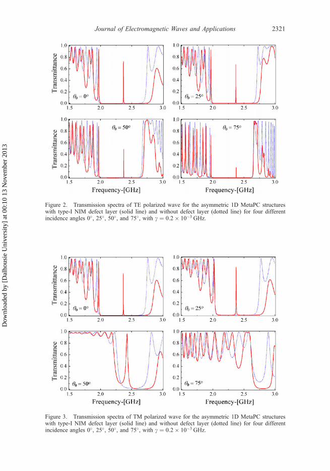
In the first part, we use Equations (4) and (5), type-I NIM, for the permittivity andthe permeability of NIM defect layer (layer C) exactly like layer A, and the transmissionspectra of two different asymmetric and symmetric geometric structures for both polar-izations are investigated. First of all, the transmission spectra of TE and TM polarizedwaves for the asymmetric structure at various angles of incidence and forc ¼ 0:2� 10�3 GHz are shown in Figures 2 and 3. As it is seen, a single resonant peakappears within the PBG, which corresponds to the type-I NIM defect layer. This is inline with the report by Wu et al. [19] for the defect modes in 1D PCs with PIMs, whereonly one defect mode for the asymmetric structure has been observed. In addition, thefigures show that as the angle of incidence increases, the peak height of the defectmode decreases for TE waves and increases for TM waves. Moreover, for both polar-izations, the frequency of the defect mode is shifted to the higher frequency as theangle increases.
2320 A. Aghajamali et al.
Dow
nloa
ded
by [
Dal
hous
ie U
nive
rsity
] at
00:
10 1
3 N
ovem
ber
2013
Figure 2. Transmission spectra of TE polarized wave for the asymmetric 1D MetaPC structureswith type-I NIM defect layer (solid line) and without defect layer (dotted line) for four differentincidence angles 0�, 25�, 50�, and 75�, with c ¼ 0:2� 10�3 GHz.
Figure 3. Transmission spectra of TM polarized wave for the asymmetric 1D MetaPC structureswith type-I NIM defect layer (solid line) and without defect layer (dotted line) for four differentincidence angles 0�, 25�, 50�, and 75�, with c ¼ 0:2� 10�3 GHz.
Journal of Electromagnetic Waves and Applications 2321
Dow
nloa
ded
by [
Dal
hous
ie U
nive
rsity
] at
00:
10 1
3 N
ovem
ber
2013
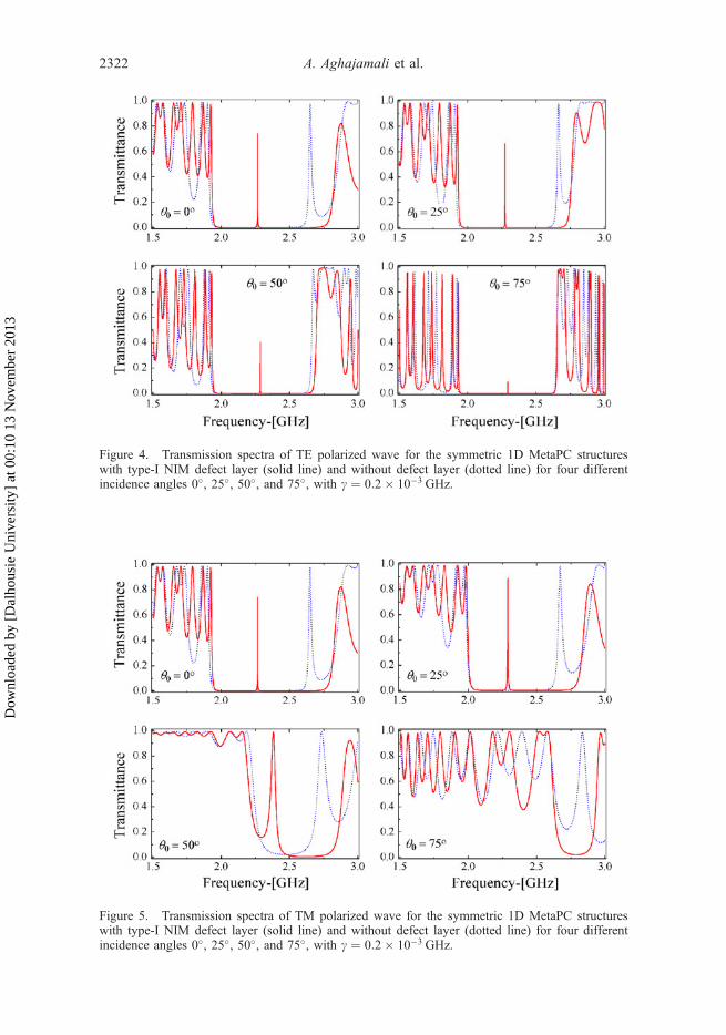
Figure 4. Transmission spectra of TE polarized wave for the symmetric 1D MetaPC structureswith type-I NIM defect layer (solid line) and without defect layer (dotted line) for four differentincidence angles 0�, 25�, 50�, and 75�, with c ¼ 0:2� 10�3 GHz.
Figure 5. Transmission spectra of TM polarized wave for the symmetric 1D MetaPC structureswith type-I NIM defect layer (solid line) and without defect layer (dotted line) for four differentincidence angles 0�, 25�, 50�, and 75�, with c ¼ 0:2� 10�3 GHz.
2322 A. Aghajamali et al.
Dow
nloa
ded
by [
Dal
hous
ie U
nive
rsity
] at
00:
10 1
3 N
ovem
ber
2013
In Figures 4 and 5, we have plotted the frequency-dependent transmittance for thesymmetric structure in TE and TM waves at four different angles of incidence. As it isobserved in these figures, similar to the asymmetric structure, there is a single defectmode within the band gap again. This is in sharp contrast to the work by Wu et al. [19]for the defect modes in 1D symmetric PC with PIMs, where there are two defectmodes. It is also worth mentioning that the number of defect modes appearing withtype-I NIM defect layer does not depend on the geometric structure, polarization, andthe angle of the incidence wave.
In more detail, as shown in Figure 6, the frequency of defect mode vs. the angle ofincidence for asymmetric (Figure 6(a)) and symmetric (Figure 6(b)) structures havebeen, respectively, plotted. As we mentioned earlier, only one defect mode appears inboth the asymmetric and symmetric structures. Additionally, as seen from the figures, inthe asymmetric structure the defect modes appear in higher frequencies when comparedto the symmetric one. Another feature in Figure 6, which is worth mentioning is thefrequency of the defect mode, which, in TE waves, remains nearly unchanged in boththe geometric structures as the angle of incidence increases. However, in TM waves,the frequency increases as the angle of incidence increases. In addition, this increase insymmetric structure is higher than that of asymmetric one.
In the second part, properties of the defect mode of both the geometric structures,with another type of NIM defect layer at the center (type-II NIM), which was describedin Section 2, are investigated. The asymmetric and symmetric structures which wereused before are modified by replacing type-II NIM defect layer (layer C), in which thepermittivity and permeability follow Equations (6) and (7). The other parameters arekept the same as the first part.
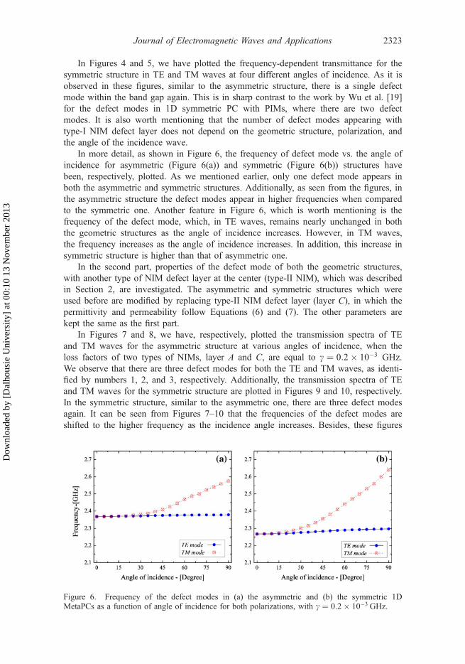
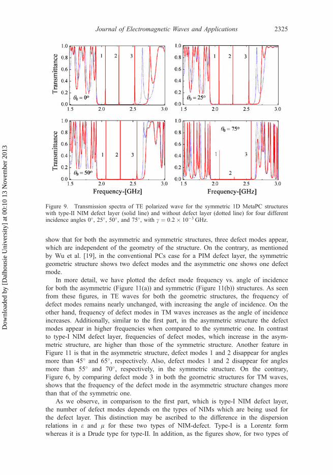
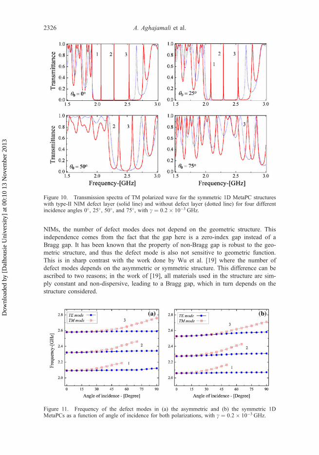
In Figures 7 and 8, we have, respectively, plotted the transmission spectra of TEand TM waves for the asymmetric structure at various angles of incidence, when theloss factors of two types of NIMs, layer A and C, are equal to c ¼ 0:2� 10�3 GHz.We observe that there are three defect modes for both the TE and TM waves, as identi-fied by numbers 1, 2, and 3, respectively. Additionally, the transmission spectra of TEand TM waves for the symmetric structure are plotted in Figures 9 and 10, respectively.In the symmetric structure, similar to the asymmetric one, there are three defect modesagain. It can be seen from Figures 7–10 that the frequencies of the defect modes areshifted to the higher frequency as the incidence angle increases. Besides, these figures
Figure 6. Frequency of the defect modes in (a) the asymmetric and (b) the symmetric 1DMetaPCs as a function of angle of incidence for both polarizations, with c ¼ 0:2� 10�3 GHz.
Journal of Electromagnetic Waves and Applications 2323
Dow
nloa
ded
by [
Dal
hous
ie U
nive
rsity
] at
00:
10 1
3 N
ovem
ber
2013
Figure 7. Transmission spectra of TE polarized wave for the asymmetric 1D MetaPC structureswith type-II NIM defect layer (solid line) and without defect layer (dotted line) for four differentincidence angles 0�, 25�, 50�, and 75�, with c ¼ 0:2� 10�3 GHz.
Figure 8. Transmission spectra of TM polarized wave for the asymmetric 1D MetaPC structureswith type-II NIM defect layer (solid line) and without defect layer (dotted line) for four differentincidence angles 0�, 25�, 50�, and 75�, with c ¼ 0:2� 10�3 GHz.
2324 A. Aghajamali et al.
Dow
nloa
ded
by [
Dal
hous
ie U
nive
rsity
] at
00:
10 1
3 N
ovem
ber
2013
show that for both the asymmetric and symmetric structures, three defect modes appear,which are independent of the geometry of the structure. On the contrary, as mentionedby Wu et al. [19], in the conventional PCs case for a PIM defect layer, the symmetricgeometric structure shows two defect modes and the asymmetric one shows one defectmode.
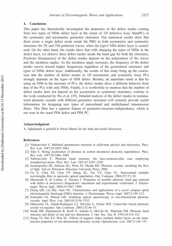
In more detail, we have plotted the defect mode frequency vs. angle of incidencefor both the asymmetric (Figure 11(a)) and symmetric (Figure 11(b)) structures. As seenfrom these figures, in TE waves for both the geometric structures, the frequency ofdefect modes remains nearly unchanged, with increasing the angle of incidence. On theother hand, frequency of defect modes in TM waves increases as the angle of incidenceincreases. Additionally, similar to the first part, in the asymmetric structure the defectmodes appear in higher frequencies when compared to the symmetric one. In contrastto type-I NIM defect layer, frequencies of defect modes, which increase in the asym-metric structure, are higher than those of the symmetric structure. Another feature inFigure 11 is that in the asymmetric structure, defect modes 1 and 2 disappear for anglesmore than 45� and 65�, respectively. Also, defect modes 1 and 2 disappear for anglesmore than 55� and 70�, respectively, in the symmetric structure. On the contrary,Figure 6, by comparing defect mode 3 in both the geometric structures for TM waves,shows that the frequency of the defect mode in the asymmetric structure changes morethan that of the symmetric one.
As we observe, in comparison to the first part, which is type-I NIM defect layer,the number of defect modes depends on the types of NIMs which are being used forthe defect layer. This distinction may be ascribed to the difference in the dispersionrelations in e and l for these two types of NIM-defect. Type-I is a Lorentz formwhereas it is a Drude type for type-II. In addition, as the figures show, for two types of
Figure 9. Transmission spectra of TE polarized wave for the symmetric 1D MetaPC structureswith type-II NIM defect layer (solid line) and without defect layer (dotted line) for four differentincidence angles 0�, 25�, 50�, and 75�, with c ¼ 0:2� 10�3 GHz.
Journal of Electromagnetic Waves and Applications 2325
Dow
nloa
ded
by [
Dal
hous
ie U
nive
rsity
] at
00:
10 1
3 N
ovem
ber
2013
NIMs, the number of defect modes does not depend on the geometric structure. Thisindependence comes from the fact that the gap here is a zero-index gap instead of aBragg gap. It has been known that the property of non-Bragg gap is robust to the geo-metric structure, and thus the defect mode is also not sensitive to geometric function.This is in sharp contrast with the work done by Wu et al. [19] where the number ofdefect modes depends on the asymmetric or symmetric structure. This difference can beascribed to two reasons; in the work of [19], all materials used in the structure are sim-ply constant and non-dispersive, leading to a Bragg gap, which in turn depends on thestructure considered.
Figure 10. Transmission spectra of TM polarized wave for the symmetric 1D MetaPC structureswith type-II NIM defect layer (solid line) and without defect layer (dotted line) for four differentincidence angles 0�, 25�, 50�, and 75�, with c ¼ 0:2� 10�3 GHz.
Figure 11. Frequency of the defect modes in (a) the asymmetric and (b) the symmetric 1DMetaPCs as a function of angle of incidence for both polarizations, with c ¼ 0:2� 10�3 GHz.
2326 A. Aghajamali et al.
Dow
nloa
ded
by [
Dal
hous
ie U
nive
rsity
] at
00:
10 1
3 N
ovem
ber
2013
4. Conclusion
This paper has theoretically investigated the properties of the defect modes comingfrom two types of NIMs defect layer at the center of 1D defective lossy MetaPCs inthe symmetric and asymmetric geometric structures. Our numerical results show thatthere exists a single defect mode inside the PBG in both asymmetric and symmetricstructures for TE and TM polarized waves, when the type-I NIM defect layer is consid-ered. On the other hand, the results show that with changing the types of NIMs in thedefect layer, we observe three defect modes inside the band gap for both the structures.Positions (frequencies) of the defect modes depend on the polarization of the wavesand the incidence angles. As the incidence angle increases, the frequency of the defectmodes moves toward higher frequencies regardless of the geometrical structures andtypes of NIMs defect layer. Additionally, the results of this study bring up the conclu-sion that the number of defect modes in 1D asymmetric and symmetric lossy PCsstrongly depends on the types of NIM defect. Besides, an important result is that byusing an NIM in the structure of PCs, the defect modes show a different behavior fromthat of the PCs with only PIMs. Finally, it is worthwhile to mention that the number ofdefect modes does not depend on the asymmetric or symmetric structures, contrary tothe work conducted by Wu et al. [19]. Detailed analysis of the defect modes in metama-terial photonic crystals with different geometric structures will certainly provide usefulinformation for designing new types of narrowband and multichannel transmissionfilters. This filter has a superior feature of geometric-structure-independence, which isnot seen in the usual PIM defect and PIM PC.
AcknowledgmentA. Aghajamali is grateful to Parisa Shams for her help and useful discussion.
References[1] Yablonovitch E. Inhibited spontaneous emission in solid-state physics and electronics. Phys.
Rev. Lett. 1987;58:2059–2062.[2] John S. Strong localization of photons in certain disordered dielectric superlattices. Phys.
Rev. Lett. 1987;58:2486–2489.[3] Yablonovitch E. Photonic band structure: the face-centered-cubic case employing
nonspherical atoms. Phys. Rev. Lett. 1991;67:2295–2298.[4] Joannopoulos JD, Johnson SG, Winn JN, Meada RD. Photonic crystals: modeling the flow
wavelengths filter in aperiodic optical superlattice. Opt. Commun. 2004;237:53–58.[6] Massaoudi S, de Lustrac A, Huynen I. Properties of metallic photonic band gap material
with defect at microwave frequencies: calculation and experimental verification. J. Electro-magn. Waves Appl. 2006;14:1967–1980.
[7] Zheng QR, Lin BQ, Yuan NC. Characteristics and applications of a novel compact spiralelectromagnetic band-gap (EBG) structure. J. Electromagn. Waves Appl. 2007;2:199–213.
[8] Schneider GJ, Watson GH. Nonlinear optical spectroscopy in one-dimensional photoniccrystals. Appl. Phys. Lett. 2003;83:5350–5352.
[10] Smith DR, Dalichaouch R, Kroll N, Schultz S, McCall SL, Platzman PM. Photonic bandstructure and defect in one and two dimension. J. Opt. Soc. Am. B. 1993;10:314–321.
[11] Xiang YJ, Dai XY, Wen SC. Effects of negative index medium defect layers on the trans-mission properties of one-dimensional photonic crystal. Optoelectron. Lett. 2007;3:144–147.
Journal of Electromagnetic Waves and Applications 2327
Dow
nloa
ded
by [
Dal
hous
ie U
nive
rsity
] at
00:
10 1
3 N
ovem
ber
2013
[12] Veselago VG. The electrodynamics of substances with simultaneously negative values of eand l . Sov. Phys. Usp. 1968;10:509–514.
[13] Lotfi E, Jamshidi-Ghaleh K, Moslem F, Masalehdan H. Comparison of photonic crystalnarrow filters with metamaterials and dielectric defects. Eur. Phys. J. D: Atomic Mol. Opt.Phys. 2010;60:369–372.
[14] Zhu Q, Zhang Y. Defect modes and wavelength tuning of one-dimensional photonic crystalwith lithium niobate. Optik 2009;120:195–198.
[15] Lyubchanskii IL, Dadoenkova NN, Zabolotin AE, Lee YP, Rasing Th. A one-dimensionalphotonic crystal with a superconducting defect layer. J. Opt. A: Pure Appl. Opt.2009;11:114014.
[16] Ansari N, Tehranchi MM, Ghanaatshoar M. Characterization of defect modes in one-dimen-sional photonic crystals: an analytic approach. Phys. B: Condensed Matter. 2009;404:1181–1186.
[17] Li X, Xie K, Jiang HM. Properties of defect modes in one-dimensional photonic crystalscontaining two nonlinear defects. Opt. Commun. 2009;282:4292–4295.
[18] Hung HC, Wu CJ, Chang SJ. A mid-infrared tunable filter in a semiconductore-dielectricphotonic crystal containing dopt semiconductore defect. Solid State Commun.2011;151:1677–1680.
[19] Wu CJ, Wang ZH. Properties of defect modes in one-dimensional photonic crystals. Prog.Electromagn. Res. 2010;103:169–184.
[20] King TC, Yang YP, Liou YS, Wu CJ. Tunable defect mode in a semiconductor-dielectricphotonic crystal containing extrinsic semiconductor defect. Solid State Commun.2012;152:2189–2192.
[21] Hu CA, Liu JW, Wu CJ, Yang TJ, Yang SL. Effects of superconducting film on the defectmode in dielectric photonic crystal heterostructure. Solid State Commun. 2013;157:54–57.
[22] Rechtaman M, Szameit A, Dreisow F, Heinrich M, Keil R, Nolte S, Segev M. Amorphousphotonic lattices: band gaps, effective mass, and suppressed transport. Phys. Rev. Lett.2011;106:193904.
[23] Ghosh S, Varshney RK, Pal BP, Monnom G. A Bragg-like chirped clad all-solid microstruc-tured optical fiber with ultra-wide bandwidth for short pulse delivery and pulse reshaping.Opt. Quant. Electron. 2010;42:1–14.
[24] Zhang W, Han P, Lan A, Li Y, Zhang X. Defect modes tuning of one-dimensional photoniccrystals with lithium niobate and silver material defect. Phys. E: Low-dimensional Syst.Nanostruct. 2012;44:813–815.
[25] Aly AH, Elsayed HA. Defect mode properties in a one-dimensional photonic crystal. Phys.B: Condensed Matter. 2012;407:120–125.
[26] Chen YH, Liang GQ, Dong JW, Wang HZ. Derivation and characterization of dispersion ofdefect modes in photonic band gap from stacks of positive and negative index materials.Phys. Lett. A 2006;351:446–451.
[27] Tang KS, Xiang YJ, Wen SC. Defect in photonic crystal with negative index material.Optoelectron. Lett. 2006;2:118–121.
[28] Jiang H, Chen H, Li H, Zhang Y. Omnidirectional gap and defect mode of one-dimensionalphotonic crystals containing negative-index materials. Appl. Phys. Lett. 2003;83:5386–5388.
[29] Wang LG, Chen H, Zhu SY. Omnidirectional gap and defect mode of one-dimensionalphotonic crystals with single-negative materials. Phys. Rev. B. 2004;70:245102.
[30] Xu Q, Xie K, Yang H, Tang J. Periodic defect modes of one-dimensional crystals containingsingle-negative materials. Optik. 2010;121:1558–1562.
[31] Xiang Y, Dai X, Wen S, Fan D. Properties of omnidirectional gap and defect mode ofone-dimensional photonic crystal containing indefinite metamaterials with a hyperbolicdispersion. J. Appl. Phys. 2007;102:093107.
[32] Wang H, Luo Y, Wang YT, Zhang HB, Fang YT. Splitting of defect-mode in one-dimen-sional magnetic photonic crystal. Phys. B: Condensed Matter. 2012;406:2977–2981.
[33] Aghajamali A, Barati M. Properties of defect modes in periodic lossy multilayer withnegative-index-materials. Commun. Theor. Phys. 2013;60:80–86.
[34] Born M, Wolf E. Principles of optics: electromagnetic theory of propagation, interferenceand diffraction of light. 7th ed. Cambridge: Cambridge University Press; 2005.
2328 A. Aghajamali et al.
Dow
nloa
ded
by [
Dal
hous
ie U
nive
rsity
] at
00:
10 1
3 N
ovem
ber
2013
[35] Zhang L, Zhang Y, He L, Wang Z, Li H, Chen H. Zero-�n gaps of photonic crystalsconsisting of positive and negative index materials in microstrip transmission lines. J. Phys.D. Appl. Phys. 2007;40:2579–2587.
[36] Li J, Zhou L, Chan CT, Sheng P. Photonic band gap from a stack of positive and negativeindex materials. Phys. Rev. Lett. 2003;90:083901.
[37] Aghajamali A, Barati M. Effects of normal and oblique incidence on zero-�n gap in periodiclossy multilayer containing double-negative materials. Phys. B: Condensed Matter.2012;407:1287–1291.
[38] Yeh P. Optical waves in layered media. Hoboken (NJ): Wiley; 1988.[39] Daninthe H, Foteinopoulou S, Soukoulis CM. Omni-reflectance and enhanced resonant
tunneling from multilayers containing left-handed materials. Photon. Nanostruct:Fundamentals Appl. 2006;4:123–131.
Journal of Electromagnetic Waves and Applications 2329