Page 1
International Journal on Electrical Engineering and Informatics - Volume 8, Number 3, September 2016
Prototype Design and Analysis of Miniature Pulse Discharge Current
Generator on Various Burdens
Waluyo, Syahrial, Sigit Nugraha, and Yudhi Permana JR
Department of Electrical Engineering
Institut Teknologi Nasional (Itenas), Bandung, Indonesia
[email protected]
Abstract: High voltage impulse is one of the means used in a variety of insulating materials
testing. It causes also discharge, generally as visualization of lightning strikes. This research
aimed to design a prototype of miniature current discharge pulse generation with various
burdens. The alternating low voltage was rectified first and multiplied by using the modified
Cockroft-Walton voltage multiplier. The yielded output voltage was a d.c. high voltage, which
subsequently entered the pulse generator circuit, penetrating the sphere gap, after filling the
charge on the first capacitor and then fill in the second capacitor. The shape of the output pulse
current was tapped by using a resistive voltage divider. Thus, the various pulse current
waveforms could be measured and recorded by a storage digital oscilloscope.
Almost first discharge were occurred in around from 1 s to 2 s. The waveforms with the
pure resistive burdens would trend to be symmetrical to almost on positive parts. On the other
hand, the waveforms with the resistive and capacitive dominated burdens would be shorter, i.e.
around 16.8 s, than those resistive dominated burdens. The wave frequency response of
discharge on the capacitive dominated burdens would more declivous or prevalent than those
on the resistive dominated burdens. The latter characteristics were indicated by the specific
capacitive dominated property. The capacitive property that store charge was expected as cause
the latter characteristics. The dominated capacitive existence made the repetitive discharge
would be shorter than those the dominated resistive existence.
Keywords: miniature, pulse, discharge, current, burden
1. Introduction
An impulse voltage is a unidirectional voltage, which generally without appreciable
oscillation, rises rapidly to a maximum value and falls more or less rapidly to zero value. Small
oscillations are tolerated, provided that their amplitudes are less than 5% of the peak values. If
the impulse voltage develops without causing flashover of puncture occur, it is called a
chopped impulse voltage. A full impulse voltage is characterized by its peak value and its two
time interval [1,2].
The actual shape of both kinds of lightning and switching over voltages varies strongly.
Nevertheless, it became necessary to simulate these transient voltages by relatively simple
means for testing purposes. The various standards define the impulse voltages as a
unidirectional voltage which rises more or less rapidly to a peak value and the decays relatively
slowly to zero. Impulse voltages with front durations varying from less than one up to a few
tens of microseconds are considered as lightning impulse generally. Lightning impulses are
very short duration, mainly if they are chopped on front [3].
Transient over voltages due to lightning and switching surges cause steep build-up of voltage
on transmission lines and other electrical apparatus. The experimental investigations showed
that these waves have a rise time of 0.5 to 10 s and decay time to 50% of the peak value of the
order 30 to 200 s. The wave shapes are arbitrary, but mostly unidirectional. It is shown that
lightning overvoltage wave can be represented as double exponential waves defined by the
equation (1).
Received: August 30th
, 2015. Accepted: September 25th
, 2016 DOI: 10.15676/ijeei.2016.8.3.2
472
Page 2
t
eteoVV (1)
where and are constants of microsecond values. This equation represents a unidirectional
wave which usually has a rapid rise to the peak value and slowly falls to zero value [4].
A simple, approximate mathematical expression for 8/20 s short circuit current waveform that
is specified in the standards is I(t), as given by equation (2).
t
etpIAtI 3 (2)
Nevertheless, for current impulses on his research results, the delay time, rise time and full
width at half-maximum values were 16.2 s, 8.02 s and 20.7 s respectively [5].
The electrical strength of high voltage apparatus against external over voltages that can
appear in power supply systems due to lightning strokes is tested with lightning impulse
voltages. The rising part of the impulse voltage is referred to as the front, the maximum as the
peak and the decreasing part as the tail. The waveforms can be represented approximately by
supervision of two exponential functions with differing time constants [6]. The standard
lighting impulse is described as a 1.2/50 s wave, and the standard switching impulse is a
250/2500 s wave [7].
A development of Matlab Simulink model has been carried out for the experimental setup
above. The results of the investigation showed that it was very efficient in the learning effect of
changes in the design parameters to obtain the impulse voltage and the desired waveform of the
impulse voltage generator for high voltage applications [8].
It has been conducted a series of simulations to adjust the formation of the output of a kind
type of Marx impulse generator. The goal was to estimate the leak capacitance and capacitance
insert into circuit simulation to effectively produce an output that was similar to the generator.
An actual three-stage impulse generator, with several different levels of impulse voltage test
and the recorded output waveform, was used as a basis. The research was carried out to
formulate the capacitance leak and identifying the location of capacitance in the generator. The
research showed that an effective simulation of the circuit could be created to provide output as
close as possible [9].
It has been made the development of Marx generator type vertical structure twenty steps. In
a matching load of 90-100, it has been obtained for 25 kV DC discharge, a pulse output voltage
230 kV, and a duration of 150 ns. This voltage pulse was applied to a relativistic electron beam
planar diode. For a cathode-anode gap of 7.5 mm, it has been obtained an REB had shot 160
kV voltage and duration of 150 ns [10].
It has been developed an impulse generator circuit using OrCAD PSpice software to
generate a waveform lightning according to IEC61000-4-5 standard. For this purpose, it has
been used as Marx generator main principles of design with a few modifications to the
parameters and components. The waveform output of the simulation compared to the surge as
IEC61000-4-5 standards, and the values in the series developed arranged so that the
characteristics of the waveform in the limits of the acceptable. As a result, the true lightning
waveforms in the form of voltage versus time were raised from an impulse generator circuit
[11].
It has been described how to calculate constant impulse voltage generator circuit with the
impulse voltage was given. From the results, it appeared that the effect of the revision of the
definition depended on the circuit constants [12].
It has been done the design, construction and analysis of the uncertainty of impulse voltage
calibrator that could be calculated. The calibrator was as the primary reference for the
measurement of impulse voltage. It generated impulse voltage with the peak, front and tail
values were known. The peak voltage range was constructed from 50 mV to 1000 V [13].
Waluyo, et al.
473
Page 3
The electrical characteristics and description of low inductance design, compact, 500 kV,
500 A, 10 Hz repetition rate, Marx generator for generating a high-power microwave source or
high power microwave (HPM) has been presented. This included the analysis of relevant
background of the Marx generator and HPM source [14].
The trigger pulses of high voltage were required for initial conduction in a triggered spark
gap that require a high impedance voltage source. This work illustrated the design, construction
and operation of two high-voltage pulse generator and a spark gap [15].
It has been presented the parameter optimization technology for the generation of lightning
current waveforms for first short stroke (10/350 μs) which was needed to test the performance
of lightning protection components, as required in IEC 62305 and IEC 62561. The crowbar
devices were specified in IEC 62305 that was applied to generate lightning current waveform.
The results, in this experiment were the new parameters of the circuit needed to be changed
because of the difference between the simulation and experimental results. An external coil
type multistage and a damping resistor have been proposed to make the generation efficiency
increased. According to these results, it was obtained by an optimization of the lightning
current waveform first short stroke [16].
Impulse generators were implemented as digital switching circuits to utilize the fast
switching speed of CMOS transistors and save power. In the single-polarity DWG prototype,
the impulse generator is designed based on a glitch generator [17].
When the analytical equations were used as an impulse source, it worked as a perfect
generator and output waveform characteristics were not dependent on the impedance of the
system. It could be confirmed that the waveform characteristics; delay time, rise time and
FWHM remain unchanged for two impedance ranges considered when used model equations
as generator sources for both voltage and current impulses. It was found that as for 1.2/50 s
voltage impulses, delay time, rise time and FWHM values were 4.95 s, 1.20 s and 81.8 s
respectively through the tested impedance range. For 8/20 s current impulses, these values
were 16.2 s, 8.02 and 20.7 s respectively throughout the tested impedance range. Hence,
characteristics of waveforms introduced to the system were not depending on the impedance of
the system and no loading effect in action under this scenario. Thus, when the analytical
equations were used as impulse sources, both voltage and current source models were
performed as ideal generators. Obviously, the waveform characteristics of the generated
impulses were varied by the influence of the nonlinear load impedance. These results implies
that the impedance of the system load be able to influence the generator characteristics. When
impedance of the nonlinear load increased, the characteristics of current impulse waveform
were also changed and significantly deviated from the expected values. However, when the
impedance was at its lowest value, these parametric values were almost equal to the values
obtained when the analytical equation was used as current impulse source. When impedance of
the nonlinear load decreased, the characteristics of voltage impulse waveform were also
deviated from the expected values. However, when the impedance was at its highest value,
these parametric values were almost equal to the values obtained when the analytical equation
was used as voltage impulse source. When the analytical equations were used as impulse
sources it worked as perfect generators and V-I characteristics were not depend on the
impedance of the system. However, V-I characteristics of the generated waveforms are varied
significantly by the impedance of the nonlinear load that was connected to the generator circuit
models. The deviations were due to influence caused by the nonlinear load to the generator
circuit parameters and effective internal impedance [5].
From some of the literature reviews, it is necessary for development in terms of the
formation of the prototype, namely in the form of utilization of high voltage generation in line
with the full-wave rectifier and utilization of high voltage multiplier results to be used as a
source of impulse voltage generation. This research was to design and implement the prototype
miniature of impulse high voltage generator based on the results of high voltage d.c. multiplier
generator.
Prototype Design and Analysis of Miniature Pulse Discharge Current
474
Page 4
The state of the art in this research was a pulse current generation in the miniature
prototype, where the sphere gap distance was also very short, around 1.5 mm, and the currents
were recorded in various burden scenarios. Thus, the phenomena of current pulse waveforms
could be understand in various burdens. For one period, these waveforms were similar to an
electrostatic discharge current. However, due to the source was direct current (dc), not a
capacitor only, the breakdown discharges were occurred in many times, instead of once. To get
some waveform phenomena, it was carried out to give four scenarios to the circuits. The
recording system was used the digital storage oscilloscope. The data could be opened, analyzed
and made curves by Excel. The data could also be made FFT analyses by using OriginPro.
Thus, the trending curves and the frequency spectra could be investigated.
Compared to the previous researches, usually, they were simulation works only, so that not
considered the distance of sphere gap, or the measurement methods those done were voltage
quantity, instead of current. Therefore, in this research, it was recorded the discharge currents
practically or in real conditions. At the analyses, the frequency responses of discharge current
waveforms were presented also. Thus, the frequency domains would be analyzed too.
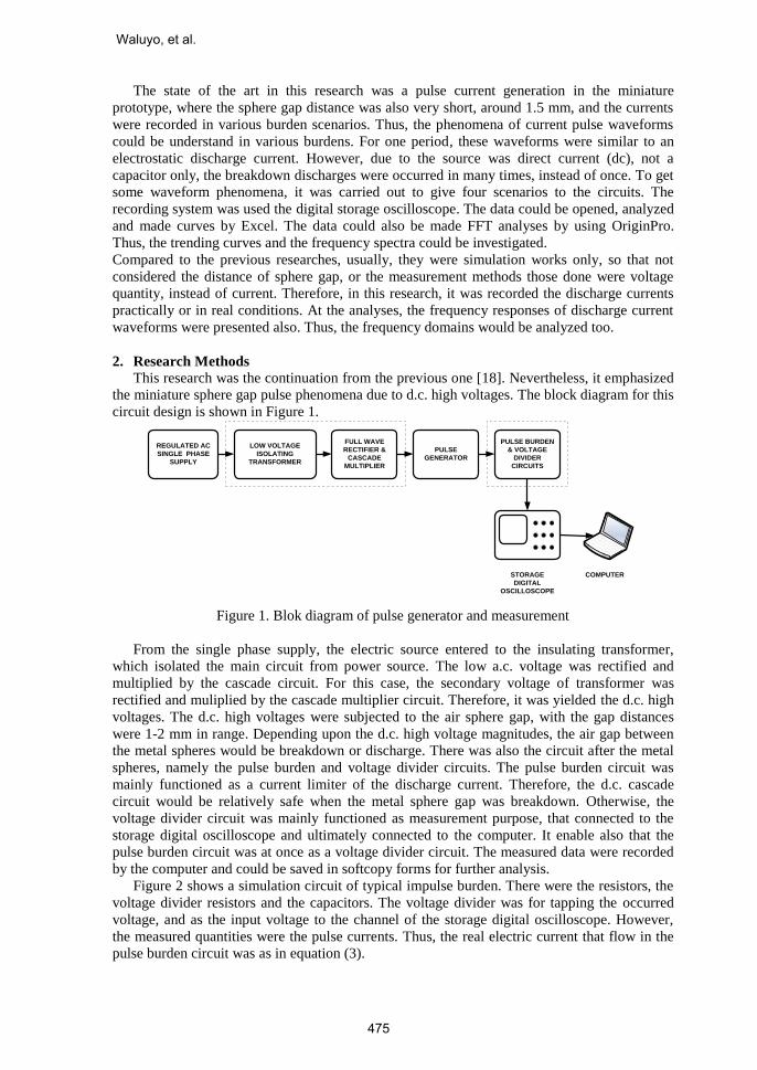
2. Research Methods
This research was the continuation from the previous one [18]. Nevertheless, it emphasized
the miniature sphere gap pulse phenomena due to d.c. high voltages. The block diagram for this
circuit design is shown in Figure 1.
REGULATED AC
SINGLE PHASE
SUPPLY
LOW VOLTAGE
ISOLATING
TRANSFORMER
FULL WAVE
RECTIFIER &
CASCADE
MULTIPLIER
PULSE
GENERATOR
PULSE BURDEN
& VOLTAGE
DIVIDER
CIRCUITS
STORAGE
DIGITAL
OSCILLOSCOPE
COMPUTER
Figure 1. Blok diagram of pulse generator and measurement
From the single phase supply, the electric source entered to the insulating transformer,
which isolated the main circuit from power source. The low a.c. voltage was rectified and
multiplied by the cascade circuit. For this case, the secondary voltage of transformer was
rectified and muliplied by the cascade multiplier circuit. Therefore, it was yielded the d.c. high
voltages. The d.c. high voltages were subjected to the air sphere gap, with the gap distances
were 1-2 mm in range. Depending upon the d.c. high voltage magnitudes, the air gap between
the metal spheres would be breakdown or discharge. There was also the circuit after the metal
spheres, namely the pulse burden and voltage divider circuits. The pulse burden circuit was
mainly functioned as a current limiter of the discharge current. Therefore, the d.c. cascade
circuit would be relatively safe when the metal sphere gap was breakdown. Otherwise, the
voltage divider circuit was mainly functioned as measurement purpose, that connected to the
storage digital oscilloscope and ultimately connected to the computer. It enable also that the
pulse burden circuit was at once as a voltage divider circuit. The measured data were recorded
by the computer and could be saved in softcopy forms for further analysis.
Figure 2 shows a simulation circuit of typical impulse burden. There were the resistors, the
voltage divider resistors and the capacitors. The voltage divider was for tapping the occurred
voltage, and as the input voltage to the channel of the storage digital oscilloscope. However,
the measured quantities were the pulse currents. Thus, the real electric current that flow in the
pulse burden circuit was as in equation (3).
Waluyo, et al.
475
Page 5
R
VI (3)
where V as the real occurred voltage that measured by the oscilloscope and R was the tapping
resistor.
Figure 2. The typical of impulse burden
In assembling of the impulse generation, the main component consisted of transformer
diodes, capacitors and resistors. The transformer which used was as step-up transformer, and as
insulation transformer, 500 watt, 0.5 ampere. The diode role was very important, where the
working principle of the diode is only issued once of the flow, either positive or negative
depending on the purposes of the output. In this assembly, it was used the diodes of
25F120/1322 type. The used capacitors were direct current with type of PAG/450Volt-100F
and the resistors were used ceramic type.
The necessary measured quantity was discharge current. However, the oscilloscope could
not measure the current quantity, instead of voltage quantity. Nevertheless, the discharge
current could be measured by the oscilloscope through series voltage divider resistors. Thus,
the discharge current phenomena could be measured indirectly and the measuring equipment
was in safe conditions. The measurements were carried out in many times. Nevertheless, they
are presented in several results only. They were typical results according to the burden
categories.
3. Research Results And Discussion
Figure 3 shows the complete assembly of research, including the sphere gap electrodes for
impulse generation that have been formed. It is seen that the input of the circuit, such as
transformer, to the output circuit, a series of impulse generation, including the sphere gap
electrode, capacitor and resistor circuits. Besides that, there were two voltmeters for voltage
measuring purposes.
Prototype Design and Analysis of Miniature Pulse Discharge Current
476
Page 6
Figure 3. The complete set of pulse generation
Figure 4 shows the miniature sphere gap for pulse generation. The distance of the sphere
gap could be adjusted. Nevertheless, in this research, it was typically 0.5 – 2.0 mm in range.
Figure 4. The sphere gap electrodes for impulse generation
(a) Resistor circuit
(b) Capacitor circuit
Figure 5. The resistor and capacitor burden circuits of pulse generation
Waluyo, et al.
477
Page 7
Figure 5(a) shows the resistors pulse burden and voltage divider circuits, whereas Figure
5(b) shows the capacitors for pulse burden circuits. Both circuits would be used as burdens of
pulse generation.
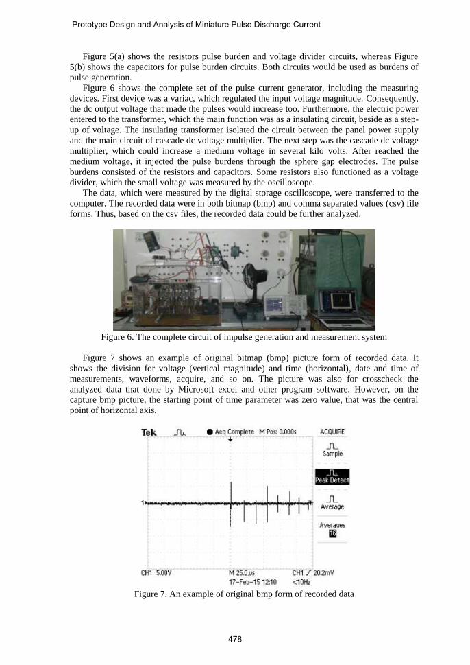
Figure 6 shows the complete set of the pulse current generator, including the measuring
devices. First device was a variac, which regulated the input voltage magnitude. Consequently,
the dc output voltage that made the pulses would increase too. Furthermore, the electric power
entered to the transformer, which the main function was as a insulating circuit, beside as a step-
up of voltage. The insulating transformer isolated the circuit between the panel power supply
and the main circuit of cascade dc voltage multiplier. The next step was the cascade dc voltage
multiplier, which could increase a medium voltage in several kilo volts. After reached the
medium voltage, it injected the pulse burdens through the sphere gap electrodes. The pulse
burdens consisted of the resistors and capacitors. Some resistors also functioned as a voltage
divider, which the small voltage was measured by the oscilloscope.
The data, which were measured by the digital storage oscilloscope, were transferred to the
computer. The recorded data were in both bitmap (bmp) and comma separated values (csv) file
forms. Thus, based on the csv files, the recorded data could be further analyzed.
Figure 6. The complete circuit of impulse generation and measurement system
Figure 7 shows an example of original bitmap (bmp) picture form of recorded data. It
shows the division for voltage (vertical magnitude) and time (horizontal), date and time of
measurements, waveforms, acquire, and so on. The picture was also for crosscheck the
analyzed data that done by Microsoft excel and other program software. However, on the
capture bmp picture, the starting point of time parameter was zero value, that was the central
point of horizontal axis.
Figure 7. An example of original bmp form of recorded data
Prototype Design and Analysis of Miniature Pulse Discharge Current
478
Page 8
Figure 8 presents the first scenario of pulse burden circuits. In this circuit, it was pure
resistive burden that parallel two 2.7 M and 300 k resistors. The measured voltage was
tapped on the 15 k resistor, which was the input of the oscilloscope.
2.7 M
2.7 M
V
285 k
15 k
DC HIGH
VOLTAGE
Figure 8. First scenario of pulse burden as short pure resistive circuit
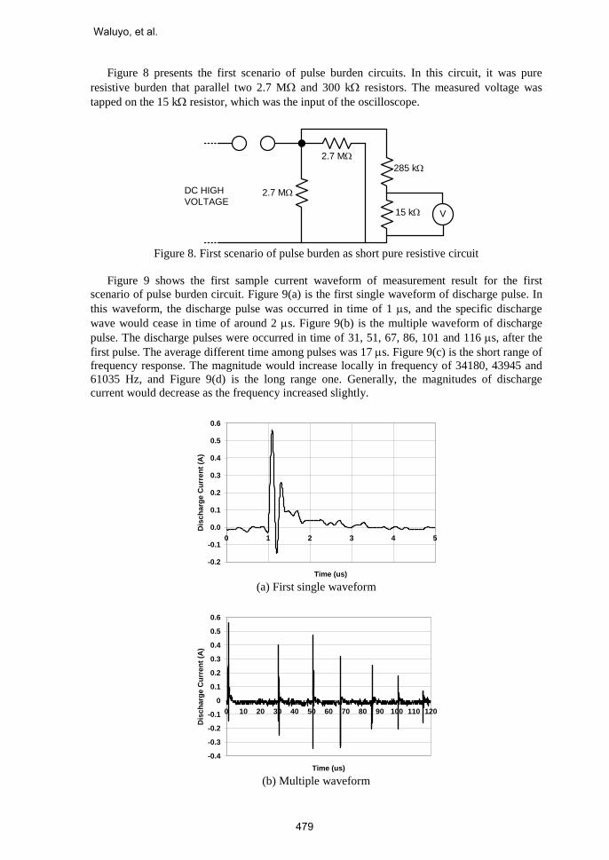
Figure 9 shows the first sample current waveform of measurement result for the first
scenario of pulse burden circuit. Figure 9(a) is the first single waveform of discharge pulse. In
this waveform, the discharge pulse was occurred in time of 1 s, and the specific discharge
wave would cease in time of around 2 s. Figure 9(b) is the multiple waveform of discharge
pulse. The discharge pulses were occurred in time of 31, 51, 67, 86, 101 and 116 s, after the
first pulse. The average different time among pulses was 17 s. Figure 9(c) is the short range of
frequency response. The magnitude would increase locally in frequency of 34180, 43945 and
61035 Hz, and Figure 9(d) is the long range one. Generally, the magnitudes of discharge
current would decrease as the frequency increased slightly.
-0.2
-0.1
0.0
0.1
0.2
0.3
0.4
0.5
0.6
0 1 2 3 4 5
Time (us)
Dis
ch
arg
e C
urr
en
t (A
)
(a) First single waveform
-0.4
-0.3
-0.2
-0.1
0
0.1
0.2
0.3
0.4
0.5
0.6
0 10 20 30 40 50 60 70 80 90 100 110 120
Time (us)
Dis
ch
arg
e C
urr
en
t (A
)
(b) Multiple waveform
Waluyo, et al.
479
Page 9
0
0.001
0.002
0.003
0.004
0.005
0.006
0.007
0.008
0.009
0.01
0.0E
+00
4.9E
+03
9.8E
+03
1.5E
+04
2.0E
+04
2.4E
+04
2.9E
+04
3.4E
+04
3.9E
+04
4.4E
+04
4.9E
+04
5.4E
+04
5.9E
+04
6.3E
+04
6.8E
+04
7.3E
+04
7.8E
+04
8.3E
+04
8.8E
+04
9.3E
+04
9.8E
+04
Frequency (Hz)
Ma
gn
itu
de
(A
)
(c) Short range of frequency response
0
0.001
0.002
0.003
0.004
0.005
0.006
0.007
0.008
0.009
0.01
0.0
E+
00
3.7
E+
04
7.3
E+
04
1.1
E+
05
1.5
E+
05
1.8
E+
05
2.2
E+
05
2.6
E+
05
2.9
E+
05
3.3
E+
05
3.7
E+
05
4.0
E+
05
4.4
E+
05
4.8
E+
05
5.1
E+
05
5.5
E+
05
5.9
E+
05
6.2
E+
05
6.6
E+
05
7.0
E+
05
7.3
E+
05
7.7
E+
05
8.1
E+
05
8.4
E+
05
8.8
E+
05
9.2
E+
05
9.5
E+
05
9.9
E+
05
Frequency (Hz)
Mag
nit
ud
e (
A)
(d) Long range of frequency response
Figure 9. First sample current waveform result for the first scenario of pulse burden circuit
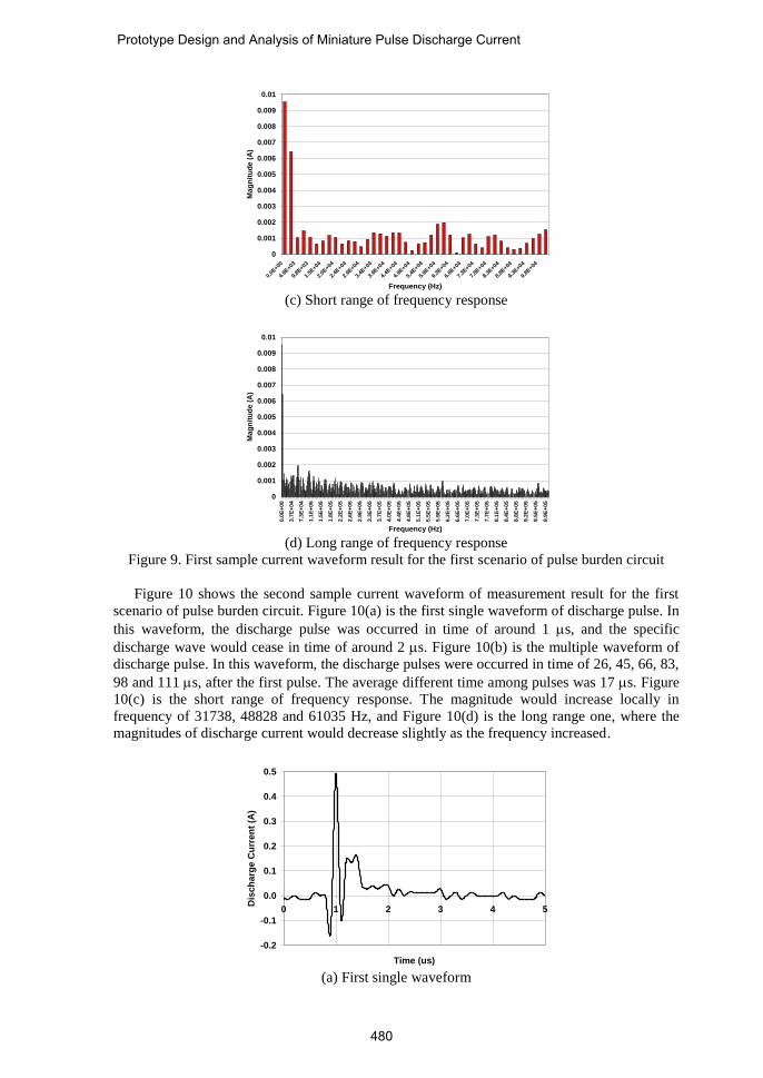
Figure 10 shows the second sample current waveform of measurement result for the first
scenario of pulse burden circuit. Figure 10(a) is the first single waveform of discharge pulse. In
this waveform, the discharge pulse was occurred in time of around 1 s, and the specific
discharge wave would cease in time of around 2 s. Figure 10(b) is the multiple waveform of
discharge pulse. In this waveform, the discharge pulses were occurred in time of 26, 45, 66, 83,
98 and 111 s, after the first pulse. The average different time among pulses was 17 s. Figure
10(c) is the short range of frequency response. The magnitude would increase locally in
frequency of 31738, 48828 and 61035 Hz, and Figure 10(d) is the long range one, where the
magnitudes of discharge current would decrease slightly as the frequency increased.
-0.2
-0.1
0.0
0.1
0.2
0.3
0.4
0.5
0 1 2 3 4 5
Time (us)
Dis
ch
arg
e C
urr
en
t (A
)
(a) First single waveform
Prototype Design and Analysis of Miniature Pulse Discharge Current
480
Page 10
-0.4
-0.3
-0.2
-0.1
0
0.1
0.2
0.3
0.4
0.5
0.6
0 10 20 30 40 50 60 70 80 90 100 110 120
Time (us)
Dis
ch
arg
e C
urr
en
t (A
)
(b) Multiple waveform
0
0.001
0.002
0.003
0.004
0.005
0.006
0.007
0.008
0.009
0.01
0.0E
+00
4.9E
+03
9.8E
+03
1.5E
+04
2.0E
+04
2.4E
+04
2.9E
+04
3.4E
+04
3.9E
+04
4.4E
+04
4.9E
+04
5.4E
+04
5.9E
+04
6.3E
+04
6.8E
+04
7.3E
+04
7.8E
+04
8.3E
+04
8.8E
+04
9.3E
+04
9.8E
+04
Frequency (Hz)
Ma
gn
itu
de
(A
)
(c) Short range of frequency response
0
0.001
0.002
0.003
0.004
0.005
0.006
0.007
0.008
0.009
0.01
0.0
E+
00
3.7
E+
04
7.3
E+
04
1.1
E+
05
1.5
E+
05
1.8
E+
05
2.2
E+
05
2.6
E+
05
2.9
E+
05
3.3
E+
05
3.7
E+
05
4.0
E+
05
4.4
E+
05
4.8
E+
05
5.1
E+
05
5.5
E+
05
5.9
E+
05
6.2
E+
05
6.6
E+
05
7.0
E+
05
7.3
E+
05
7.7
E+
05
8.1
E+
05
8.4
E+
05
8.8
E+
05
9.2
E+
05
9.5
E+
05
9.9
E+
05
Frequency (Hz)
Ma
gn
itu
de
(A
)
(d) Long range of frequency response
Figure 10. Second sample current waveform result for the first scenario of pulse burden circuit
2.7 M
2.7 M
V
285 k
15 k
DC HIGH
VOLTAGE
Figure 11. Second scenario of pulse burden as long pure resistive circuit
Waluyo, et al.
481
Page 11
Figure 11 shows the second scenario of pulse burden circuits. In this circuit, it was pure
resistive burden that parallel an 2.7 M and 300 k resistors, and in series with resistor of 2.7
M.
Figure 12 shows the first sample current waveform of measurement result for the second
scenario of pulse burden circuit. Figure 12(a) is the first single waveform of discharge pulse. In
this waveform, the discharge pulse was occurred in time of around 1 s, and the specific
discharge wave would cease in time of around 2 s. Figure 12(b) is the multiple waveform of
discharge pulse. In this waveform, the discharge pulses were occurred in time of 30, 54, 74, 92
and 111 s, after the first pulse. The average different time among pulses was 20 s. Figure
12(c) is the short range of frequency response. The magnitude would increase locally in
frequency of 26855, 36621 and 53711 Hz, and Figure 12(d) is the long range one. The
magnitudes of discharge current would decrease slightly as the frequency increased.
-0.2
-0.1
0.0
0.1
0.2
0.3
0.4
0.5
0.6
0.7
0 1 2 3 4 5
Time (us)
Dis
ch
arg
e C
urr
en
t (A
)
(a) First single waveform
-0.4
-0.3
-0.2
-0.1
0
0.1
0.2
0.3
0.4
0.5
0.6
0.7
0 10 20 30 40 50 60 70 80 90 100 110 120
Time (us)
Dis
ch
arg
e C
urr
en
t (A
)
(b) Multiple waveform
0
0.001
0.002
0.003
0.004
0.005
0.006
0.007
0.008
0.009
0.01
0.0E
+00
4.9E
+03
9.8E
+03
1.5E
+04
2.0E
+04
2.4E
+04
2.9E
+04
3.4E
+04
3.9E
+04
4.4E
+04
4.9E
+04
5.4E
+04
5.9E
+04
6.3E
+04
6.8E
+04
7.3E
+04
7.8E
+04
8.3E
+04
8.8E
+04
9.3E
+04
9.8E
+04
Frequency (Hz)
Mag
nit
ud
e (
A)
(c) Short range of frequency response
Prototype Design and Analysis of Miniature Pulse Discharge Current
482
Page 12
0
0.001
0.002
0.003
0.004
0.005
0.006
0.007
0.008
0.009
0.01
0.0
E+
00
3.7
E+
04
7.3
E+
04
1.1
E+
05
1.5
E+
05
1.8
E+
05
2.2
E+
05
2.6
E+
05
2.9
E+
05
3.3
E+
05
3.7
E+
05
4.0
E+
05
4.4
E+
05
4.8
E+
05
5.1
E+
05
5.5
E+
05
5.9
E+
05
6.2
E+
05
6.6
E+
05
7.0
E+
05
7.3
E+
05
7.7
E+
05
8.1
E+
05
8.4
E+
05
8.8
E+
05
9.2
E+
05
9.5
E+
05
9.9
E+
05
Frequency (Hz)
Ma
gn
itu
de
(A
)
(d) Long range of frequency response
Figure 12. First sample current waveform result for the second scenario of pulse burden circuit
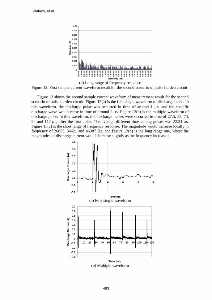
Figure 13 shows the second sample current waveform of measurement result for the second
scenario of pulse burden circuit. Figure 13(a) is the first single waveform of discharge pulse. In
this waveform, the discharge pulse was occurred in time of around 1 s, and the specific
discharge wave would cease in time of around 2 s. Figure 13(b) is the multiple waveform of
discharge pulse. In this waveform, the discharge pulses were occurred in time of 27.5, 53, 73,
94 and 112 s, after the first pulse. The average different time among pulses was 22.24 s.
Figure 13(c) is the short range of frequency response. The magnitude would increase locally in
frequency of 26855, 36621 and 46387 Hz, and Figure 13(d) is the long range one, where the
magnitudes of discharge current would decrease slightly as the frequency increased.
-0.2
-0.1
0.0
0.1
0.2
0.3
0.4
0.5
0 1 2 3 4 5
Time (us)
Dis
ch
arg
e C
urr
en
t (A
)
(a) First single waveform
-0.4
-0.3
-0.2
-0.1
0
0.1
0.2
0.3
0.4
0.5
0.6
0.7
0 10 20 30 40 50 60 70 80 90 100 110 120
Time (us)
Dis
ch
arg
e C
urr
en
t (A
)
(b) Multiple waveform
Waluyo, et al.
483
Page 13
0
0.001
0.002
0.003
0.004
0.005
0.006
0.007
0.008
0.009
0.0E
+00
4.9E
+03
9.8E
+03
1.5E
+04
2.0E
+04
2.4E
+04
2.9E
+04
3.4E
+04
3.9E
+04
4.4E
+04
4.9E
+04
5.4E
+04
5.9E
+04
6.3E
+04
6.8E
+04
7.3E
+04
7.8E
+04
8.3E
+04
8.8E
+04
9.3E
+04
9.8E
+04
Frequency (Hz)
Mag
nit
ud
e (
A)
(c) Short range of frequency response
0
0.001
0.002
0.003
0.004
0.005
0.006
0.007
0.008
0.009
0.0
E+
00
3.7
E+
04
7.3
E+
04
1.1
E+
05
1.5
E+
05
1.8
E+
05
2.2
E+
05
2.6
E+
05
2.9
E+
05
3.3
E+
05
3.7
E+
05
4.0
E+
05
4.4
E+
05
4.8
E+
05
5.1
E+
05
5.5
E+
05
5.9
E+
05
6.2
E+
05
6.6
E+
05
7.0
E+
05
7.3
E+
05
7.7
E+
05
8.1
E+
05
8.4
E+
05
8.8
E+
05
9.2
E+
05
9.5
E+
05
9.9
E+
05
Frequency (Hz)
Mag
nit
ud
e (
A)
(d) Long range of frequency response
Figure 13. Second sample current waveform result for the second scenario of pulse burden
circuit
Figure 14 shows the third scenario of pulse burden circuits. In this circuit, it was pure 2.7
M resistive burden that series with 300 k resistor and series 15x10 F in parallel. Those
component were parallel connection with the resistor of 2.7 M.
2.7 M
V
285 k
15 k
15x10F
in Series
DC HIGH
VOLTAGE2.7 M
Figure 14. Third scenario of pulse burden as short capacitive-resistive circuit
Figure 15 shows the first sample current waveform of measurement result for the third
scenario of pulse burden circuit. Figure 15(a) is the first single waveform of discharge pulse. In
this waveform, the discharge pulse was occurred in time of around 1 s, and the specific
discharge wave would cease in time of around 2 s. Figure 15(b) is the multiple waveform of
discharge pulse. In this waveform, the discharge pulses were occurred in time of 27.5, 53, 73,
Prototype Design and Analysis of Miniature Pulse Discharge Current
484
Page 14
94 and 112 s, after the first pulse. The average different time among pulses was 22.24 s.
Figure 15(c) is the short range of frequency response. The magnitude would increase locally in
frequency of 61035 Hz, and Figure 15(d) shows the long range one, where the magnitudes of
discharge current would decrease slightly as the frequency increased.
-0.8
-0.7
-0.6
-0.5
-0.4
-0.3
-0.2
-0.1
0
0.1
0.2
0.3
0.4
0.5
0 1 2 3 4 5
Time (us)
Dis
ch
arg
e C
urr
en
t (A
)
(a) First single waveform
-25,000
-20,000
-15,000
-10,000
-5,000
0
5,000
10,000
15,000
20,000
0 10 20 30 40 50 60 70 80 90 100 110 120
TIME (uS)
VO
LT
AG
E (
V)
(b) Multiple waveform
0
0.005
0.01
0.015
0.02
0.025
0.03
0.035
0.04
0.045
0.05
0.0
E+
00
4.9
E+
03
9.8
E+
03
1.5
E+
04
2.0
E+
04
2.4
E+
04
2.9
E+
04
3.4
E+
04
3.9
E+
04
4.4
E+
04
4.9
E+
04
5.4
E+
04
5.9
E+
04
6.3
E+
04
6.8
E+
04
7.3
E+
04
7.8
E+
04
8.3
E+
04
8.8
E+
04
9.3
E+
04
9.8
E+
04
Frequency (Hz)
Ma
gn
itu
de
(A
)
(c) Short range of frequency response
Waluyo, et al.
485
Page 15
0
0.005
0.01
0.015
0.02
0.025
0.03
0.035
0.04
0.045
0.05
0.0
E+
00
3.7
E+
04
7.3
E+
04
1.1
E+
05
1.5
E+
05
1.8
E+
05
2.2
E+
05
2.6
E+
05
2.9
E+
05
3.3
E+
05
3.7
E+
05
4.0
E+
05
4.4
E+
05
4.8
E+
05
5.1
E+
05
5.5
E+
05
5.9
E+
05
6.2
E+
05
6.6
E+
05
7.0
E+
05
7.3
E+
05
7.7
E+
05
8.1
E+
05
8.4
E+
05
8.8
E+
05
9.2
E+
05
9.5
E+
05
9.9
E+
05
Frequency (Hz)
Ma
gn
itu
de
(A
)
(d) Long range of frequency response
Figure 15. First sample current waveform result for the third scenario of pulse burden circuit
Figure 16 shows the second sample current waveform of measurement result for the third
scenario of pulse burden circuit. Figure 16(a) is the first single waveform of discharge pulse. In
this waveform, the discharge pulse was occurred in time of around 1 s, and the specific
discharge wave would cease in time of around 2 s. Figure 16(b) is the multiple waveform of
discharge pulse. In this waveform, the discharge pulses were occurred in time of 21, 43.6, 61,
81 and 107.6 s, after the first pulse. The average different time among pulses was 21.32 s.
Figure 16(c) is the short range of frequency response. The magnitude would increase locally in
frequency of 36621 and 48828 Hz, and Figure 16(d) is the long range, that similar to the
previous one.
-0.2
-0.1
0
0.1
0.2
0.3
0.4
0.5
0.0 1.0 2.0 3.0 4.0 5.0
Time (us)
Dis
ch
arg
e C
urr
en
t (A
)
(a) First single waveform
-0.5
-0.4
-0.3
-0.2
-0.1
0
0.1
0.2
0.3
0.4
0.5
0.6
0.7
0 10 20 30 40 50 60 70 80 90 100 110 120
Time (us)
Dis
ch
arg
e C
urr
en
t (A
)
(b) Multiple waveform
Prototype Design and Analysis of Miniature Pulse Discharge Current
486
Page 16
0
0.005
0.01
0.015
0.02
0.025
0.03
0.035
0.0E
+00
4.9E
+03
9.8E
+03
1.5E
+04
2.0E
+04
2.4E
+04
2.9E
+04
3.4E
+04
3.9E
+04
4.4E
+04
4.9E
+04
5.4E
+04
5.9E
+04
6.3E
+04
6.8E
+04
7.3E
+04
7.8E
+04
8.3E
+04
8.8E
+04
9.3E
+04
9.8E
+04
Frequency (Hz)
Ma
gn
itu
de
(A
)
(c) Short range of frequency response
0
0.005
0.01
0.015
0.02
0.025
0.03
0.035
0.0
E+
00
3.7
E+
04
7.3
E+
04
1.1
E+
05
1.5
E+
05
1.8
E+
05
2.2
E+
05
2.6
E+
05
2.9
E+
05
3.3
E+
05
3.7
E+
05
4.0
E+
05
4.4
E+
05
4.8
E+
05
5.1
E+
05
5.5
E+
05
5.9
E+
05
6.2
E+
05
6.6
E+
05
7.0
E+
05
7.3
E+
05
7.7
E+
05
8.1
E+
05
8.4
E+
05
8.8
E+
05
9.2
E+
05
9.5
E+
05
9.9
E+
05
Frequency (Hz)
Ma
gn
itu
de
(A
)
(d) Long range of frequency response
Figure 16. Second sample current waveform result for the third scenario of pulse burden circuit
Figure 17 shows the fourth scenario of pulse burden circuit. In this circuit, it was pure 2.7
M resistive burden that series with 300 k resistor that shunted by 15x10 F in parallel.
2.7 M
V
285 k
15 k
15x10F
in Series
DC HIGH
VOLTAGE
Figure 17. Fourth scenario of pulse burden as long capacitive-resistive circuit
Figure 18 shows the first sample current waveform of measurement result for the fourth
scenario of pulse burden circuit. Figure 18(a) shows the first single waveform of discharge
pulse. In this waveform, the discharge pulse was occurred in time of around 1 s, and the
specific discharge wave would cease in time of around 2 s. Figure 18(b) shows the multiple
waveform of discharge pulse. In this waveform, the discharge pulses were occurred in time of
0.9, 21.1, 39.3, 56.1, 72.3, 89.9, 104.3 and 118.3 s, after the first pulse. Nevertheless, almost
pulses were negative values. The average different time among pulses was 16.8 s. Figure 18(c)
is the short range of frequency response. The magnitude would increase locally in frequency of
Waluyo, et al.
487
Page 17
26855 Hz, and Figure 18(d) is the long range one, where the current magnitudes remained
relatively high.
-0.6
-0.5
-0.4
-0.3
-0.2
-0.1
0.0
0.1
0.2
0.3
0.4
0 1 2 3 4 5
Time (uS)
Dis
ch
arg
e C
urr
en
t (A
)
(a) First single waveform
-0.6
-0.5
-0.4
-0.3
-0.2
-0.1
0
0.1
0.2
0.3
0.4
0 10 20 30 40 50 60 70 80 90 100 110 120
Time (us)
Dis
ch
arg
e C
urr
en
t (A
)
(b) Multiple waveform
0
0.005
0.01
0.015
0.02
0.025
0.03
0.035
0.04
0.0E
+00
2.0E
+04
3.9E
+04
5.9E
+04
7.8E
+04
9.8E
+04
1.2E
+05
1.4E
+05
1.6E
+05
1.8E
+05
2.0E
+05
2.1E
+05
2.3E
+05
2.5E
+05
2.7E
+05
2.9E
+05
3.1E
+05
3.3E
+05
3.5E
+05
3.7E
+05
3.9E
+05
Frequency (Hz)
Ma
gn
itu
de
(A
)
(c) Short range of frequency response
Prototype Design and Analysis of Miniature Pulse Discharge Current
488
Page 18
0
0.005
0.01
0.015
0.02
0.025
0.03
0.035
0.04
0.0
E+
00
1.5
E+
05
2.9
E+
05
4.4
E+
05
5.9
E+
05
7.3
E+
05
8.8
E+
05
1.0
E+
06
1.2
E+
06
1.3
E+
06
1.5
E+
06
1.6
E+
06
1.8
E+
06
1.9
E+
06
2.1
E+
06
2.2
E+
06
2.3
E+
06
2.5
E+
06
2.6
E+
06
2.8
E+
06
2.9
E+
06
3.1
E+
06
3.2
E+
06
3.4
E+
06
3.5
E+
06
3.7
E+
06
3.8
E+
06
4.0
E+
06
Frequency (Hz)
Ma
gn
itu
de
(A
)
(d) Long range of frequency response
Figure 18. First sample current waveform result for the fourth scenario of pulse burden circuit
Figure 19 shows the second sample current waveform of measurement result for the fourth
scenario of pulse burden circuit. Figure 19(a) is the first single waveform of discharge pulse. In
this waveform, the discharge pulse was occurred in time of around 0.75 s, and the specific
discharge wave would cease in time of around 1.5 s. Figure 19(b) is the multiple waveform of
discharge pulse. In this waveform, the discharge pulses were occurred in time of 0.9, 20.7, 40.5,
59.5, 74.9, 89.7, 105.3 and 118.3 s, after the first pulse. Nevertheless, almost pulses were
negative values. The average different time among pulses was 16.8 s. Figure 19(c) is the short
range of frequency response. The magnitude would increase locally in frequency of 48828 Hz,
and Figure 19(d) is the long range one, where the current magnitudes remained relatively high.
-0.6
-0.4
-0.2
0.0
0.2
0.4
0.6
0 1 2 3 4 5
Time (uS)
Dis
ch
arg
e C
urr
en
t (V
)
(a) First single waveform
-0.6
-0.5
-0.4
-0.3
-0.2
-0.1
0
0.1
0.2
0.3
0.4
0 10 20 30 40 50 60 70 80 90 100 110 120
Time (us)
Dis
ch
arg
e C
urr
en
t (A
)
(b) Multiple waveform
Waluyo, et al.
489
Page 19
0
0.005
0.01
0.015
0.02
0.025
0.03
0.035
0.0E
+00
2.0E
+04
3.9E
+04
5.9E
+04
7.8E
+04
9.8E
+04
1.2E
+05
1.4E
+05
1.6E
+05
1.8E
+05
2.0E
+05
2.1E
+05
2.3E
+05
2.5E
+05
2.7E
+05
2.9E
+05
3.1E
+05
3.3E
+05
3.5E
+05
3.7E
+05
3.9E
+05
Frequency (Hz)
Ma
gn
itu
de
(A
)
(c) Short range of frequency response
0
0.005
0.01
0.015
0.02
0.025
0.03
0.035
0.0
E+
00
1.5
E+
05
2.9
E+
05
4.4
E+
05
5.9
E+
05
7.3
E+
05
8.8
E+
05
1.0
E+
06
1.2
E+
06
1.3
E+
06
1.5
E+
06
1.6
E+
06
1.8
E+
06
1.9
E+
06
2.1
E+
06
2.2
E+
06
2.3
E+
06
2.5
E+
06
2.6
E+
06
2.8
E+
06
2.9
E+
06
3.1
E+
06
3.2
E+
06
3.4
E+
06
3.5
E+
06
3.7
E+
06
3.8
E+
06
4.0
E+
06
Frequency (Hz)
Ma
gn
itu
de
(A
)
(d) Long range of frequency response
Figure 19. Second sample current waveform result for the fourth scenario of pulse burden
circuit
Table 1. Time of discharge and frequency response due to some circuit scenarios
Scenario Impulse
burdens
Times of discharge
(s)
Averages different
time of discharge (s)
Frequencies of
increasing magnitude
locally (Hz)
1
Short pure
resistive
circuit
31, 51, 67, 86, 101,
116 17 34180, 43945, 61035
26, 45, 66, 83, 98, 111 17 31738, 48828, 61035
2
Long pure
resistive
circuit
30, 54, 74, 92, 111 20 26855, 36621, 53711
27.5, 53, 73, 94, 112 22.24 26855, 36621, 46387
3
Short
resistive-
capacitive
circuit
27.5, 53, 73, 94, 112 22.24 61035
21,43.6, 61, 81, 107.6 21.32 36621, 48828
4
Short
resistive-
capacitive
circuit
0.9, 21.1, 39.3, 56.1,
72.3, 89.9, 104.3,
118.3
16.8 26855
0.9, 20.7, 40.5, 59.5,
74.9, 89.7, 105.3,
118.3
16.8 48828
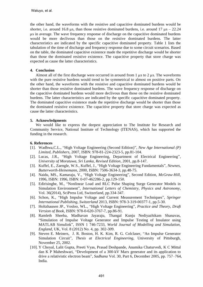
Based on some discharge waveforms of testing results, it is observed that the waveforms
with the pure resistive burdens would trend to be symmetrical to almost on positive parts. On
Prototype Design and Analysis of Miniature Pulse Discharge Current
490
Page 20
the other hand, the waveforms with the resistive and capacitive dominated burdens would be
shorter, i.e. around 16.8 s, than those resistive dominated burdens, i.e. around 17 s – 22.24
s in average. The wave frequency response of discharge on the capacitive dominated burdens
would be more declivous than those on the resistive dominated burdens. The latter
characteristics are indicated by the specific capacitive dominated property. Table 1 lists the
tabulation of the time of discharge and frequency response due to some circuit scenarios. Based
on the table, the dominated capacitive existence made the repetitive discharge would be shorter
than those the dominated resistive existence. The capacitive property that store charge was
expected as cause the latter characteristics.
4. Conclusion
Almost all of the first discharge were occurred in around from 1 s to 2 s. The waveforms
with the pure resistive burdens would trend to be symmetrical to almost on positive parts. On
the other hand, the waveforms with the resistive and capacitive dominated burdens would be
shorter than those resistive dominated burdens. The wave frequency response of discharge on
the capacitive dominated burdens would more declivous than those on the resistive dominated
burdens. The latter characteristics are indicated by the specific capacitive dominated property.
The dominated capacitive existence made the repetitive discharge would be shorter than those
the dominated resistive existence. The capacitive property that store charge was expected as
cause the latter characteristics.
5. Acknowledgments
We would like to express the deepest appreciation to The Institute for Research and
Community Service, National Institute of Technology (ITENAS), which has supported the
funding in the research.
6. References
[1]. Wadhwa,C.L., “High Voltage Engineering (Second Edition)”, New Age International (P)
Limited, Publishers, 2007, ISBN: 978-81-224-2323-5, pp.81-104.
[2]. Lucas, J.R., “High Voltage Engineering, Department of Electrical Engineering”,
University of Moratuwa, Sri Lanka, Revised Edition, 2001, pp.8-147.
[3]. Kuffel, E., Zaengle, W.S., Kuffel, J., “High Voltage Engineering Fundamentals”, Newnes,
Butterworth-Heinemann, 2000, ISBN: 7506-3634-3, pp.48-75.
[4]. Naidu, MS., Kamaraju, V., “High Voltage Engineering”, Second Edition, McGraw-Hill,
1996, ISBN: 1996, ISBN: 0-07-462286-2, pp.129-150.
[5]. Edirisinghe, M., “Nonlinear Load and RLC Pulse Shaping Surge Generator Models in
Simulation Environment”, International Letters of Chemistry, Physics and Astronomy,
Vol. 36(2014), SciPress Ltd, Switzerland, pp.334-347.
[6]. Schon, K., “High Impulse Voltage and Current Measurement Techniques”, Springer
International Publishing, Switzerland 2013, ISBN: 978-3-319-00377-1, pp.5-30.
[7]. Holtzhausen JP., Vosloo, WL., “High Voltage Engineering”, Practice and Theory, Draft
Version of Book, ISBN: 978-0-620-3767-7, pp.86-91.
[8]. Ramleth Sheeba, Madhavan Jayaraju, Thangal Kunju Nediyazhikam Shanavas,
“Simulation of Impulse Voltage Generator and Impulse Testing of Insulator using
MATLAB Simulink”, ISSN 1 746-7233, World Journal of Modelling and Simulation,
England, UK, Vol. 8 (2012) No. 4, pp. 302-309.
[9]. Steven E. Meiners, J. R. Boston, H. K. Kim, R. G. Colclaser, “An Impulse Generator
Simulation Circuit”, Thesis at Electrical Engineering, University of Pittsburgh,
November 25, 2002.
[10]. Y Choyal, Lalit Gupta, Preeti Vyas, Prasad Deshpande, Anamika Chaturvedi, K C Mittal
dan K P Maheshwari, “Development of a 300-kV Marx generator and its application to
drive a relativistic electron beam”, Sadhana Vol. 30, Part 6, December 2005, pp. 757–764,
India.
Waluyo, et al.
491
Page 21
[11]. Muhammad Saufi Kamarudin, Erwan Sulaiman, Md Zarafi Ahmad, Shamsul Aizam
Zulkifli and Ainul Faiza Othman, “Impulse Generator and Lightning Characteristics
Simulation using Orcad PSpice Software”, Proceedings of EnCon2008, 2nd Engineering
Conference on Sustainable Engineering Infrastructures Development & Management,
December 18 -19, 2008, Kuching, Sarawak, Malaysia.
[12]. Takayoshi Nakata, Yoshiyuki Ishihara dan Tadataka Moriyasu, “Calculation of Circuit
Constants for Impulse Voltage Generator by Means of Computer”, Memoirs of The
School of Engineering, Okayama University, Vol. 1, No.1, March, 1966.
[13]. Jari Hallstro, “A Calculable Impulse Voltage Calibrator, Acta Polytechnica Scandinavia”,
Electrical Engineering Series No. 109, Espoo 2002, 107, Finnish Academies of
Technology, Finland, 2002, ISBN: 951-22-6174-X, pp.60-70.
[14]. Yeong-Jer Chen, B.S.E.E., Andreas Neuber, John Mankowski, “Compact Repetitive
Marx Generator and HPM Generation with the Vircator”, Electrical Engineering
Graduate, Faculty of Texas Tech University, December, 2005.
[15]. A.A. Hueiit, E. Bautista, L.J. Villegast Anij M. Villagiian, “High voltage pulse generators
and spark gap for gaseous discharge control”, Instrumentación Revista Mexicana de
Física 41, No. 3,1995, pp.08-.18.
[16]. Ju-Hong Eom, Sung-Chul Cho† and Tae-Hyung Lee*, “Parameters Optimization of
Impulse Generator Circuit for Generating First Short Stroke Lightning Current
Waveform”, J Electr Eng Technol Vol. 9, No. 1: 286-292, 2014.
[17]. Zhu, Y., Zuegel, J.D., Marciante, J.R., Wu, H., “Distributed Waveform Generator: A New
Circuit Technique for Ultra-Wideband Pulse Generation, Shaping and Modulation”, IEEE
Journal of Solid-State Circuits, Vol. 44, No. 3, March 2009, pp.808-823.
[18]. Waluyo, Syahrial, Sigit Nugraha, Yudhi Permana JR, “Miniature Prototype Design and
Implementation of Modified Multiplier Circuit DC High Voltage Generator”,
International Journal of Electrical Engineering & Technology (IJEET), International
Association for Engineering and Management Education (IAEME), Volume 6, Issue 1,
January (2015), pp. 01-12.
Waluyo was born in Magelang, Indonesia in 1969. He received B.Eng.,
M.Eng., and Doctor Degrees in electrical engineering from Bandung Insitute
of Technology (ITB), Indonesia, in 1994, 2002 and 2010 respectively. Since
2003, he is a Lecturer at Department of Electrical Engineering, National
Institute of Technology (Itenas) Bandung, Indonesia. His research interests
include of high voltage phenomena. He received Best Lecturer in Kopertis
IV in 2013.
Syahrial was born in Lirik, Sumatera, Indonesia in 1969. He received B.Eng.,
Degree in electrical engineering from National Insitute of Technology (Itenas)
Bandung, Indonesia, in 2000, and M.Eng. Degree in electrical engineering
from Bandung Insitute of Technology (ITB), Indonesia, in 2004. Since 2005,
he is a Lecturer at Department of Electrical Engineering, National Institute of
Technology (Itenas) Bandung, Indonesia. His research interests include of
electrical machines.
Prototype Design and Analysis of Miniature Pulse Discharge Current
492
Page 22
Sigit Nugraha was born in Subang, West Java, Indonesia. He is currently
senior university student and doing final project at The Department of
Electrical Engineering, National Institute of Technology (Itenas) Bandung,
Indonesia.
Yudhi Permana JR was born in Padang, West Sumatera, Indonesia. He is
currently senior university student and doing final project at The Department
of Electrical Engineering, National Institute of Technology (Itenas) Bandung,
Indonesia.
Waluyo, et al.
493