1 Prototyping stacked modules for the L1 track trigger tbc Aachen (tbc) D. Newbold, C. Hill Bristol University D. Abbaneo, K. Gill, A. Marchioro CERN P. Hobson Brunel University A. Ryd Cornell University tbc DESY G. Hall, M. Raymond Imperial College London N Bacchetta INFN Padova G.M. Bilei, A Santocchia INFN Perugia L. DeMaria INFN Torino F. Hartmann Karlsruhe D. Contardo Lyon K. Ecklund Rice University C Shepherd-Themistocleous Rutherford Appleton Laboratory tbc Strasbourg (tbc) J Incandela University of California Santa Barbara M. Krammer Vienna Contact persons: G. Hall ([email protected]), A. Ryd ([email protected]) Abstract: This proposal describes a research program with the goal of prototyping and testing a tracker module capable of providing track trigger primitives as required for the CMS tracker in the Super-LHC Phase 2 upgrade.
Transcript
1
Prototyping stacked modules for the L1 track trigger
tbc Aachen (tbc)
D. Newbold, C. Hill Bristol University
D. Abbaneo, K. Gill, A. Marchioro CERN
P. Hobson Brunel University
A. Ryd Cornell University
tbc DESY
G. Hall, M. Raymond Imperial College London
N Bacchetta INFN Padova
G.M. Bilei, A Santocchia INFN Perugia
L. DeMaria INFN Torino
F. Hartmann Karlsruhe
D. Contardo Lyon
K. Ecklund Rice University
C Shepherd-Themistocleous Rutherford Appleton Laboratory
tbc Strasbourg (tbc)
J Incandela University of California Santa Barbara
This proposal describes a research program with the goal of prototyping and testing a tracker module capable of providing track trigger primitives as required for the CMS tracker in the Super-LHC Phase 2 upgrade.
2
1. Introduction It is generally agreed that for the SLHC at an instantaneous luminosity of 1035 cm-2s-1, or ten times the design
luminosity of the LHC, the current trigger based on muons plus hadronic and electromagnetic calorimetry will need to be enhanced with information from the Tracker [ref]. The total L1 trigger rate, without use of Tracker data, is expected to exceed the nominal limit of 100kHz by a large factor, probably exceeding an order of magnitude.
The challenge is a little different for each type of trigger. For muons the goal is primarily to add tracking information to discriminate between different muon chamber hit combinations which appear to make valid muon trajectories. Using muon data alone at SLHC will include many fakes and thus does not provide a reliable momentum estimate for the L1 trigger. For electrons the challenge is to associate hits in the tracker with calorimeter objects to reject backgrounds from photons. The requirements for taus are not yet so clear but the present jet trigger has a rate far higher than acceptable and improved isolation of tracks associated with tau jets appears, from HLT experience, to offer a means to reduce the raw trigger rate. In addition, to the tasks above we would like to be able to provide vertexing capabilities in the L1 trigger.
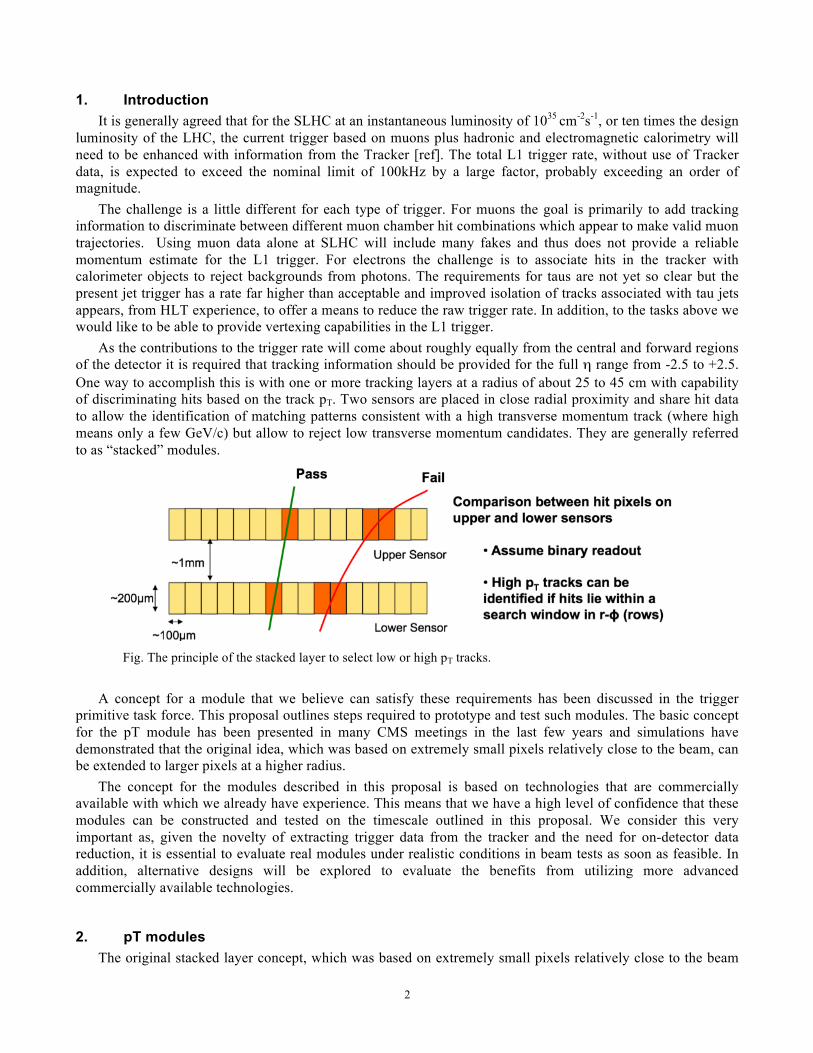
As the contributions to the trigger rate will come about roughly equally from the central and forward regions of the detector it is required that tracking information should be provided for the full η range from -2.5 to +2.5. One way to accomplish this is with one or more tracking layers at a radius of about 25 to 45 cm with capability of discriminating hits based on the track pT. Two sensors are placed in close radial proximity and share hit data to allow the identification of matching patterns consistent with a high transverse momentum track (where high means only a few GeV/c) but allow to reject low transverse momentum candidates. They are generally referred to as “stacked” modules.
Fig. The principle of the stacked layer to select low or high pT tracks.
A concept for a module that we believe can satisfy these requirements has been discussed in the trigger
primitive task force. This proposal outlines steps required to prototype and test such modules. The basic concept for the pT module has been presented in many CMS meetings in the last few years and simulations have demonstrated that the original idea, which was based on extremely small pixels relatively close to the beam, can be extended to larger pixels at a higher radius.
The concept for the modules described in this proposal is based on technologies that are commercially available with which we already have experience. This means that we have a high level of confidence that these modules can be constructed and tested on the timescale outlined in this proposal. We consider this very important as, given the novelty of extracting trigger data from the tracker and the need for on-detector data reduction, it is essential to evaluate real modules under realistic conditions in beam tests as soon as feasible. In addition, alternative designs will be explored to evaluate the benefits from utilizing more advanced commercially available technologies.
2. pT modules The original stacked layer concept, which was based on extremely small pixels relatively close to the beam
3
[ref], can be extended to larger pixels at a higher radius. This is vital for the tracking system since it is highly undesirable to add significant material at low radii and it will be very challenging to approach the low material budgets already demonstrated in the present pixel system using trigger layers in the inner pixels. Further material reductions are expected in the Phase I pixel upgrade and there are strong reasons to consider it undesirable to worsen this aspect of the future Tracker design.
In this proposal we consider track-trigger modules that we believe can be constructed using technologies in common use today. This is important as it is crucial to be able to demonstrate that these modules work and provide the required functionality in beam tests over the next few years. We will need this information in order to write a tracker (and trigger) TDR. It is also important that we can actually build these modules. In this proposal we consider two slightly different types of modules which differ in assembly method, including how interconnects between the two sensor layers are done.
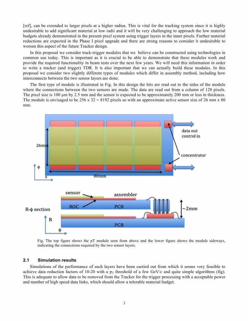
The first type of module is illustrated in Fig. In this design the hits are read out to the sides of the module where the connections between the two sensors are made. The data are read out from a column of 128 pixels. The pixel size is 100 µm by 2.5 mm and the sensor is expected to be approximately 200 mm or less in thickness. The module is envisaged to be 256 x 32 = 8192 pixels so with an approximate active sensor size of 26 mm x 80 mm.
Fig. The top figure shows the pT module seen from above and the lower figure shows the module sideways, indicating the connections required by the two sensor layers.
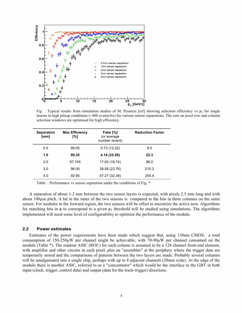
2.1 Simulation results Simulations of the performance of such layers have been carried out from which it seems very feasible to
achieve data reduction factors of 10-20 with a pT threshold of a few GeV/c and quite simple algorithms (fig). This is adequate to allow data to be removed from the Tracker for the trigger processing with a acceptable power and number of high speed data links, which should allow a tolerable material budget.
4
Fig . Typical results from simulation studies of M. Pesaresi [ref] showing selection efficiency vs pT for single muons in high pileup conditions (~400 events/bx) for various sensor separations. The cuts on pixel row and column selection windows are optimised for high efficiency.
Separation
[mm] Max Efficiency
[%] Fake [%]
(or average number /event)
Reduction Factor
0.5 99.05 0.73 (12.22) 8.0
1.0 99.35 4.14 (25.58) 22.3
2.0 97.745 17.83 (18.74) 96.0
3.0 96.00 39.08 (23.76) 210.3
4.0 92.95 47.27 (32.39) 254.4
Table . Performance vs sensor separation under the conditions of Fig. *
A separation of about 1-2 mm between the two sensor layers is expected, with pixels 2.5 mm long and with about 100µm pitch. A hit in the inner of the two sensors is compared to the hits in three columns on the outer sensor. For modules in the forward region, the two sensors will be offset to maximize the active area. Algorithms for matching hits in φ to correspond to a given pT threshold will be studied using simulations. The algorithms implemented will need some level of configurability to optimize the performance of the module.
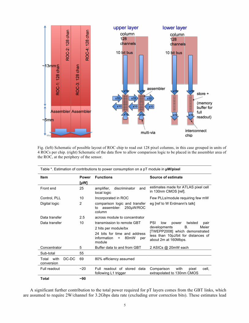
2.2 Power estimates Estimates of the power requirements have been made which suggest that, using 130nm CMOS, a total
consumption of 150-250µW per channel might be achievable, with 70-90µW per channel consumed on the module (Table *). The readout ASIC (ROC) for each column is assumed to be a 128 channel front-end element, with amplifier and other circuits in each pixel, plus an "assembler" at the periphery where the trigger data are temporarily stored and the comparisons of patterns between the two layers are made. Probably several columns will be amalgamated into a single chip, perhaps with up to 8 adjacent channels (20mm wide). At the edge of the module there is another ASIC, referred to as a "concentrator" which would be the interface to the GBT in both input (clock, trigger, control data) and output (data for the track-trigger) directions.
5
Fig. (left) Schematic of possible layout of ROC chip to read out 128 pixel columns, in this case grouped in units of 4 ROCs per chip. (right) Schematic of the data flow to allow comparison logic to be placed in the assembler area of the ROC, at the periphery of the sensor.
A significant further contribution to the total power required for pT layers comes from the GBT links, which
are assumed to require 2W/channel for 3.2Gbps data rate (excluding error correction bits). These estimates lead
Table *. Estimation of contributions to power consumption on a pT module in µW/pixel
Item Power [µW]
Functions Source of estimate
Front end 25 amplifier, discriminator and local logic
estimates made for ATLAS pixel cell in 130nm CMOS [ref].
Control, PLL 10 Incorporated in ROC Few PLLs/module requiring few mW Digital logic 2 comparison logic and transfer
to assembler: 250µW/ROC column
eg [ref to W Erdmann's talk]
Data transfer 2.5 across module to concentrator Data transfer 10 transmission to remote GBT
2 hits per module/bx 24 bits for time and address information = 80mW per module
PSI low power twisted pair developments B. Meier [TWEPP2008] which demonstrated less than 10pJ/bit for distances of about 2m at 160Mbps.
Concentrator 5 Buffer data to and from GBT 2 ASICs @ 20mW each Sub-total 55 Total with DC-DC conversion
69 80% efficiency assumed
Full readout ~20 Full readout of stored data following L1 trigger
Comparison with pixel cell, extrapolated to 130nm CMOS
Total ~90
6
to a requirement for 1000 GBT links to read out a layer of about 40M pixels at radius of 25cm, assuming a data reduction factor of 20 and an occupancy of 0.5% and 24 bits transmitted for each selected pixel. However, these figures also assume 100% use of the GBT bandwidth which is not very likely. A more realistic figure might be 50\% use of the GBT, so doubling the link power requirement to 6kW for the layer. The GBT transceivers should be located outside the sensitive Tracker volume, probably in the region presently occupied by the TEC bulkhead. They will present difficult challenges to cool such a large number of transmitters and for component density.
The total power consumption for stacked layers with these pixel dimensions can be estimated [GH last talk] to be about 9kW for 40M pixels at 25 cm radius, and 17kW for 75M pixels at 35 cm radius. The total number of links required is 2900 and 5600 for the two cases; this does not allow for full readout of the layers, only track-trigger data. These layers will therefore represent the major contribution to power consumption of a likely layout of a new Tracker and great care will be needed not to allow either power, material or numbers of links to increase significantly if the tracking performance is to be maintained.
On-detector logic The ROC logic should reject large clusters which could not be consistent with a high pT track. For the pixel
dimensions considered, the occupancy is estimated, by simulations and extrapolations of values at 1034 cm-2s-1 to be less than 0.5% at 1035 cm-2s-1. This is sufficiently low that most columns will be empty and one hit per column is the most likely case. Double hits in a column will occur but are most likely to be from charge sharing between pixels. A method which would allow to read out small numbers of hits in each 40MHz clock cycle has been proposed [GH] so that the comparison logic can be placed at the periphery of the module. If this scheme proves not to be sufficiently robust at the maximum occupancy, alternatives will be studied, such as transferring data to the periphery at 80MHz.
This logic and module design allows the material to be minimized underneath the active region of the sensor, which has advantages in reducing secondary interactions and multiple scattering which would affect the efficiency of correlating hits from the two sensor layers. As the module design progresses it will be possible to evaluate more rigorously the total material and attempt to optimise it. At present, this concept also seems to be the most economical way of accessing the data by avoiding transferring data at high speed between pixels in the two layers of the stack.
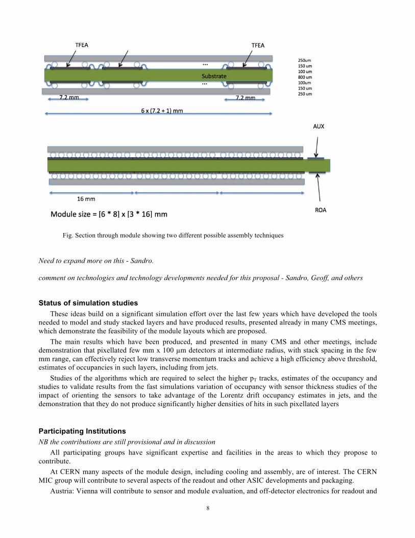
However, since the logical design is at a very early stage and this is a new area, it is important to understand well the trade-offs in decision logic by comparing with alternative concepts. It is also possible that module assembly issues will prove to be important in manufacturing pT modules on a large scale. Therefore a second type of module design will also be developed (fig from Sandro) in which data will be transferred through an intermediate substrate from one pixel layer to another. It seems that this may be achieved using advanced assembly methods which are already in widespread use in industry and this is being explored with potential vendors.
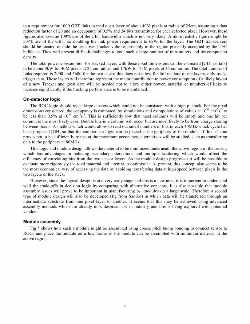
Module assembly Fig * shows how such a module might be assembled using coarse pitch bump bonding to connect sensor to
ROCs and place the module on a low frame so the module can be assembled with minimum material in the active region.
7
Fig. Schematic of a possible assembly sequence
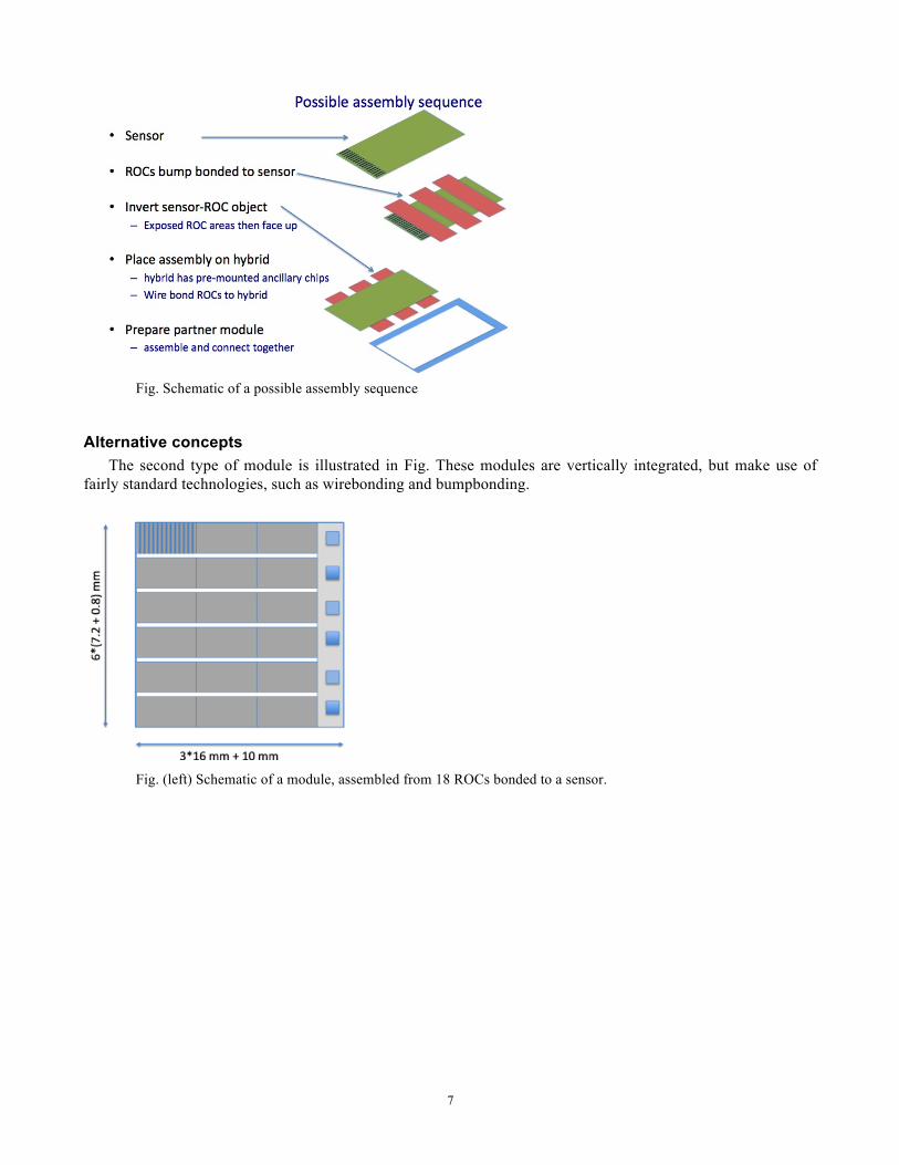
Alternative concepts The second type of module is illustrated in Fig. These modules are vertically integrated, but make use of
fairly standard technologies, such as wirebonding and bumpbonding.
Fig. (left) Schematic of a module, assembled from 18 ROCs bonded to a sensor.
8
Fig. Section through module showing two different possible assembly techniques Need to expand more on this - Sandro. comment on technologies and technology developments needed for this proposal - Sandro, Geoff, and others
Status of simulation studies These ideas build on a significant simulation effort over the last few years which have developed the tools
needed to model and study stacked layers and have produced results, presented already in many CMS meetings, which demonstrate the feasibility of the module layouts which are proposed.
The main results which have been produced, and presented in many CMS and other meetings, include demonstration that pixellated few mm x 100 µm detectors at intermediate radius, with stack spacing in the few mm range, can effectively reject low transverse momentum tracks and achieve a high efficiency above threshold, estimates of occupancies in such layers, including from jets.
Studies of the algorithms which are required to select the higher pT tracks, estimates of the occupancy and studies to validate results from the fast simulations variation of occupancy with sensor thickness studies of the impact of orienting the sensors to take advantage of the Lorentz drift occupancy estimates in jets, and the demonstration that they do not produce significantly higher densities of hits in such pixellated layers
Participating Institutions NB the contributions are still provisional and in discussion
All participating groups have significant expertise and facilities in the areas to which they propose to contribute.
At CERN many aspects of the module design, including cooling and assembly, are of interest. The CERN MIC group will contribute to several aspects of the readout and other ASIC developments and packaging.
Austria: Vienna will contribute to sensor and module evaluation, and off-detector electronics for readout and
9
module control (tbc). France: Lyon (tbc). Strasbourg (tbc) Germany: Karlsruhe will contribute to sensor design and evaluation. DESY will contribute to mechanical
aspects of module development. Aachen (tbc) Italy: Perugia will contribute to …, including evaluation studies. Torino will contribute to ASIC electronics
and module development. Padova… UK: Imperial College will contribute to the tasks of performing simulation studies, developing the readout
chip and detector evaluations. Bristol will are interested in simulations and aspects of module design as well as contributing to the logic and readout development. Rutherford Appleton Laboratory…
USA: Cornell will contribute to simulation studies and off-detector electronics for module evaluation and participation in test beams and data analysis. Rice…. Santa Barbara will contribute to module development, including mechanical and thermal studies, simulations and electronic developments.
Topics and goals of the R&D proposal Below is a description of the R&D activities that are proposed within this proposal. The goal of the proposal
is to demonstrate a module that will satisfy the requirements for providing track trigger primitives for the SLHC phase II upgrade by 2012.
Simulation - design studies Contributions to this section from CU + IC
The ROC and the associated logic for forming the track stubs should be simulated in detail to understand the performance of the algorithms implemented. This work will build on the studies done within the track trigger primitive simulation group.
Some of the goals for these studies involve: Each pixel will have an adjustable threshold. For pixels having a charge deposit above this threshold a
clustering algorithm will be applied. This clustering algorithm could be implemented as a pattern that requires 2(3) or less pixels in a column. It can also be investigated to perform a two dimensional clustering where correlations are made across columns.
A column consists of 128 pixels in the strawman layout. One concept is that we would accept at most one cluster per column. The impact on the efficiency from only accepting on cluster per column has to be studied. It has to be justified that this approach will work in dense tracking environments such as jets without any significant loss of efficiency. Results to date are encouraging.
The algorithm for comparing the found clusters in the two different stack members will need to be simulated to explore the efficiency for finding the track segments.
We will take the patterns of hits from the detector simulation and use as input to the electronic simulation to predict the digital power associated with the logic.
We will simulate the data volume produced by the proposed algorithms and the performance of the data concentrator chip.
The tools for doing these simulations are now (mostly) in place. We have the fast and full simulation
working for different stacked detector geometries. We need to produce code that emulates the proposed hardware implementations at the 'bit level'.
The results from these studies will guide the development of the readout chip.
10
ROC design and digital logic Contributions to this section from IC+CERN
This is the design of the analog readout chip done in 130 nm technology.
Data concentrator and control Contributions to this section from CERN
The 'data concentrator' chip as indicated in Fig. XXX has multiple purposes. (Similar in some sense to the pixel TBM chip.) It will provide the interface for distribution of clocks, triggers, and other programming of the ROC, and it will also coordinate the readout of many ROCs and concentration of the data to better utilize the bandwidth of the links.
We should consider if we can develop the first prototype module without this data concentrator chip. See further discussion in the section on prototype evaluation. Can we use GBT (prototypes) for this? (Will they be available?)
Sensor Contributions to this section from Perugia
Likely, there will be another submission the HPK sometime in early 2010. We should establish a collaboration with the existing sensor effort to make a prototype sensor that is compatible with the module proposed in this proposal.
Module power Contributions from Aachen? Katja Klein?
Module assembly Contributions to this section from CU+IC+CERN (D.A. and K.G.)
There are many engineering issues that must be addressed in assembling this type of module: Detailed layout of the module. Interconnection between the two sensors. Cooling. Mechanical support, and material budget.
Module evaluation Contributions to this section from CU + Padova?
The goal is to test these modules in a beam test, see next section. In order to program and readout these modules we will need to have a test stand that is able to interface these modules. What is required here will depend a bit on the exact plan for prototyping these modules. In particular, if will include the data concentrator chip in the (first) prototype or not.
11
Some of the requirements for the test stand include:
Clock generation. Program/initialize the front ends, including the track trigger primitive generation. Distribution of triggers. Including L0 triggers? Charge injection generation. (Calsynch triggers.) Synchronization with test beam pulses. Readout data. What rate? Prescaling?
Are there existing test setups that we can use, or develop from? Can we use commercial test boards. (Discuss with Mark Raymond.) Would we want to build on existing CMS electronics (TTC, FECs, etc.)? I'm not sure that this would make sense as most of this is likely to be replaced in the future, and is a rather complicated setup.
Beam test Contributions to this section from CU + others?
It is crucial to test the performance of these PT modules in a test beam. As Lorentz drift is an important issue for the performance of these modules we need to be able to test these modules in a magnetic field. Goals from the test beam would include:
Study the hit efficiency Study the cluster size and clustering efficiency. Study the pT turn-on for different target thresholds. Noise measurements It will be necessary to anticipate these beam tests well in advance so suitable ancillary equipment is available
to carry out the tests. This will include a suitable beam telescope to measure trajectories of incident and outgoing particles, possibly at more than one downstream location in case secondary particles are generated, eg using a simple target, and the ability to rotate the pT module under test to study features such as charge sharing.
Activities The 'activity matrix' for the proposed R&D is shown in Table. NB very provisional!!
Institution Simulation
ASIC Off-detector electronics
Sensor Module development
Module evaluation
beam test
Cornell X X X
Imperial X X X X X
Bristol X X X X
RAL X X X X
CERN X X X X X
Perugia X X
Karlsruhe X
Vienna X X X
UCSB X X X
Rice X X
12
Torino X X X X
Padova
R&D program Below is a list of the goals of this R&D program: Simulate 'at the bit level' the functionality of the pT module. This will guide the development of the
module electronic. Understand how mechanically and electrically we can integrate one of these modules. This includes
cooling. Prototype the module and test it with a source and beam. ...
Year 2009 2010 2011 2012
Q1 Q2 Q3 Q4 Q1 Q2 Q3 Q4 Q1 Q2 Q3 Q4 Q1 Q2 Q3 Q4
Simulation X X X X X
ROC
Digital
Concentrator
Sensor
Module
Evaluation
Beam test
Relation to other WG and R&D activities
Schedule
The goal is to have prototype modules that have been tested in a test beam by the end of 2012. This is a rather ambitious goal, even though we are employing techniques that are well understood in our community. The schedule is shown in Table ….
The initial work will involve further simulation studies. This builds on the work done by the track-trigger simulation group, but will focus on a more detailed simulation of the performance and requirements of the proposed readout chip. The plan is to start the design of the ROC, including the related correlation logic, by early 2010. The simulation work will continue in parallel to refine the algorithms. At the same time as the ROC is being defined we will need to design the sensor. Later in 2010 we will start the work on the module and evaluation tools as the specific interfaces with the ROC and module are being specified. The last year will be devoted to evaluation and beam tests, but will probably also involve iterations on different components.


![OUTDOOR POWER EQUIPMENT · [tbc] tbc-270pfds 20 tbc-270pfs 17 tbc-270s 17 tbc-270sfs 24 tbc-290 18 tbc-290d 20 tbc-290s 18 tbc-340 18 tbc-340d 21 tbc-340ds 21 tbc-340pf 18 tbc-340pfd](https://static.documents.pub/doc/80x56/5e2726727836ca4a7e750b4c/outdoor-power-equipment-tbc-tbc-270pfds-20-tbc-270pfs-17-tbc-270s-17-tbc-270sfs.jpg)


![TBC [Recovered]](https://static.documents.pub/doc/80x56/577c84481a28abe054b843da/tbc-recovered.jpg)


