MultiCraft International Journal of Engineering, Science and Technology Vol. 7, No. 1, 2015, pp. 44-58 INTERNATIONAL JOURNAL OF ENGINEERING, SCIENCE AND TECHNOLOGY www.ijest-ng.com www.ajol.info/index.php/ijest 2015 MultiCraft Limited. All rights reserved PSO-based optimization of PI regulator and VA loading of a SRF-based multi-converter DVR P. Vasudeva Naidu 1 *, B. Basavaraja 2 1* Department of Electrical & Electronics Engineering, GITAM University, INDIA 2 Department of Electrical & Electronics Engineering, UBDT Engineering College (VTU), Davanagere, INDIA * Corresponding Author: e-mail: [email protected], [email protected] Tel +91-9440141343 Abstract This paper deals with a design of optimal parameters of PI regulator in voltage control loop. The design aims to minimize volt- ampere (VA) loading of synchronous reference frame (SRF) based multi converter-DVR in parallel feeder distribution systems. To improve the power quality by using power conditioner with multi converters in each feeder distribution system under different load considerations, a dynamic model of synchronous-reference- frame (SRF) has been adopted. It is desirable to have optimization of PI components and generate the reference compensate voltages for series active filters (SAF) of MC-DVR. Therefore, series active filters help to inject optimal voltages at optimal angle in such a way that a minimum VA loading of MC- DVR is possible. The optimal value PI components and optimal series injected angle of series active power filters are computed using particle swarm optimization (PSO) technique and the results are verified with genetic algorithm (GA). The simulation results show that the proposed PSO technique causes minimum error and minimum VA loading angle by optimally choosing parameters of PI and minimum VA angle as compared to GA technique. Keywords: Active power filter (APF), synchronous reference frame (SRF), Genetic algorithm (GA), Particle Swarm Optimization (PSO) and multi converter dynamic voltage restorer (MC-DVR). DOI: http://dx.doi.org/10.4314/ijest.v7i1.5 1. Introduction Increased usage of electronic controllers and switched apparatus in domestic and industries, is leading to several power-quality (PQ) problems (Bollen, 2003) such as harmonics, Voltage flickers, Voltage sags, etc. Some sensitive loads require a pure A.C supply voltage for proper functioning of load necessitating a solution to the power quality problems (Ray Arnold, 2001). A few years back passive filters and active filters started being used in combination with the conventional converters to meet power quality standards (Reid, 1996). Presently, using custom power devices customers gain in terms of cost and quality of power. Custom power devices are also used for mitigating power quality issues like voltage/current unbalances, harmonics, poor power factor, sag/swells and interruptions. Broadly, custom power devices are classified as shunt active power filters, Series active power filters, and combined shunt-series active power filters (APFs) (Fujita and Akagi, 1998). Shunt active power filters are connected in a shunt arrangement with load and usually called Distribution Static Compensator (D-STATCOM) (Hague, 2001). They are used for mitigating current related power quality problems like reactive power compensation, harmonic elimination and load balancing. Series Active Power Filter (SEAPF) is connected in series with the load and is also called as Dynamic Voltage Restorer (DVR). DVR (Wang et al, 2006) is used for overcoming voltage related power quality issues like sag/swell, voltage harmonics and unbalances in voltages quantities in power distribution systems. The current research focuses on controlling the power flow of an entire line (Aredes et al, 1998) rather than a sub network or a portion of a line, to extend the DVR with the help of multi converter to control the power flow of the entire line rather than a portion of a line (Jindal et al, 2009). This paper presents the PSO-based voltage controlled loop and minimization of volt-ampere loading of the synchronous- reference-frame (SRF) (Rodríguez et al, 2007) based multi converter-DVR (MC-DVR). MC-DVR which consists of two series
Transcript
MultiCraft
International Journal of Engineering, Science and Technology Vol. 7, No. 1, 2015, pp. 44-58
INTERNATIONAL JOURNAL OF
ENGINEERING, SCIENCE AND TECHNOLOGY
www.ijest-ng.com www.ajol.info/index.php/ijest
2015 MultiCraft Limited. All rights reserved
PSO-based optimization of PI regulator and VA loading of a SRF-based
multi-converter DVR
P. Vasudeva Naidu1*, B. Basavaraja2
1*Department of Electrical & Electronics Engineering, GITAM University, INDIA 2 Department of Electrical & Electronics Engineering, UBDT Engineering College (VTU), Davanagere, INDIA
Abstract This paper deals with a design of optimal parameters of PI regulator in voltage control loop. The design aims to minimize volt-ampere (VA) loading of synchronous reference frame (SRF) based multi converter-DVR in parallel feeder distribution systems. To improve the power quality by using power conditioner with multi converters in each feeder distribution system under different load considerations, a dynamic model of synchronous-reference- frame (SRF) has been adopted. It is desirable to have optimization of PI components and generate the reference compensate voltages for series active filters (SAF) of MC-DVR. Therefore, series active filters help to inject optimal voltages at optimal angle in such a way that a minimum VA loading of MC-DVR is possible. The optimal value PI components and optimal series injected angle of series active power filters are computed using particle swarm optimization (PSO) technique and the results are verified with genetic algorithm (GA). The simulation results show that the proposed PSO technique causes minimum error and minimum VA loading angle by optimally choosing parameters of PI and minimum VA angle as compared to GA technique. Keywords: Active power filter (APF), synchronous reference frame (SRF), Genetic algorithm (GA), Particle Swarm Optimization (PSO) and multi converter dynamic voltage restorer (MC-DVR). DOI: http://dx.doi.org/10.4314/ijest.v7i1.5 1. Introduction Increased usage of electronic controllers and switched apparatus in domestic and industries, is leading to several power-quality (PQ) problems (Bollen, 2003) such as harmonics, Voltage flickers, Voltage sags, etc. Some sensitive loads require a pure A.C supply voltage for proper functioning of load necessitating a solution to the power quality problems (Ray Arnold, 2001). A few years back passive filters and active filters started being used in combination with the conventional converters to meet power quality standards (Reid, 1996). Presently, using custom power devices customers gain in terms of cost and quality of power. Custom power devices are also used for mitigating power quality issues like voltage/current unbalances, harmonics, poor power factor, sag/swells and interruptions. Broadly, custom power devices are classified as shunt active power filters, Series active power filters, and combined shunt-series active power filters (APFs) (Fujita and Akagi, 1998). Shunt active power filters are connected in a shunt arrangement with load and usually called Distribution Static Compensator (D-STATCOM) (Hague, 2001). They are used for mitigating current related power quality problems like reactive power compensation, harmonic elimination and load balancing. Series Active Power Filter (SEAPF) is connected in series with the load and is also called as Dynamic Voltage Restorer (DVR). DVR (Wang et al, 2006) is used for overcoming voltage related power quality issues like sag/swell, voltage harmonics and unbalances in voltages quantities in power distribution systems. The current research focuses on controlling the power flow of an entire line (Aredes et al, 1998) rather than a sub network or a portion of a line, to extend the DVR with the help of multi converter to control the power flow of the entire line rather than a portion of a line (Jindal et al, 2009). This paper presents the PSO-based voltage controlled loop and minimization of volt-ampere loading of the synchronous-reference-frame (SRF) (Rodríguez et al, 2007) based multi converter-DVR (MC-DVR). MC-DVR which consists of two series
Naidu and Basavaraja / International Journal of Engineering, Science and Technology, Vol. 7, No. 1, 2015, pp. 44-58
45
voltage source converters (VSC-1 and VSC-2) which are connected back to back with the help of common dc capacitor Cdc. The VSCs are 3-level (H-bridge) inverters which work independently and they work on the output feedback synchronous reference frame (SRF) based Control (Kesler and Ozdemir, 2009) with help of PI regulator. By using GA and PSO techniques optimal PI regulator components (Kp and Ki) are found which reduce the steadystate error in voltage controlled loop. After minimizing the steady state error to generate reference voltage signals and switching signals to VSC1 and VSC2 by sinusoidal PWM generator constant the dc-link voltage .Which is used to find the switching times above converters, such that their bus voltages and currents can be accurately traced as per requirement. Here feeder1 employs VSC1 in series with PCC bus-1 and feeder2 employs VSC2 in series with PCC bus-2 which are as shown in figure 1. The two VSCs are formed by the combination of reactor (Lf), ac filter capacitors (Cf) and three phase converters to prevent the flow of the harmonic currents into the distribution system generated due to switching at each phase of PCC. The voltages at PCC bus1 and bus2 along with load voltage are regulated by MC-DVR (Jindal et al 2008). It also regulates against voltage sags and swells and voltage harmonic content (vh) with minimum VA loading. The minimum real power injection (Yashomani et al, 2007) of the MC-DVR has also been achieved with the voltage injection by series active filter at an optimum angle with respect to source voltage. In this paper, the effects of both source voltage and the VA loading of MC-DVR are minimized by injecting a series active filter voltage at an optimum angle with respect to the sag voltage. The proposed methodology ensures that the minimum VA loading (Shady Hossam Eldeen Abdel Aleem et al, 2012) is obtained by Genetic Algorithm (GA) and Particle Swarm Optimization technique (PSO) (Saravanan et al, 2007). Which are utilized as tools for evaluating the optimum angle of voltage injection with constraints on THD of load voltages. Simulation results on a power distribution system are carried out and results are presented.
Figure 1.The single line diagram of conventional MC-DVR
2. Modelling 2.1 MC-DVR dynamic model
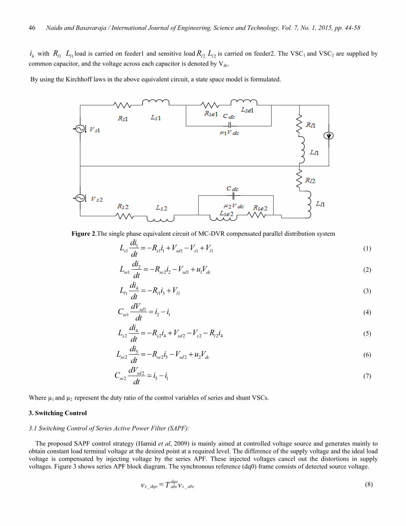
The considered electrical circuit is a two feeder, three-phase three-wire system. Figure 1 shows the internal connections of the MC-DVR, with VSCs, load and the power network.The VSCs are used for injection of controllable voltage µ1Vdc, and µ2Vdc in order to control load voltage and PCC bus voltages under the closed loop. The dc link voltage may be self-supported by a dc link capacitor for the case of MC-DVR. Figure 2 shows the single line diagram of of conventional MC-DVR compensated parallel feeder distribution system. The Filters that are connected across both the inverters are represented by 1seL 1seC and 2seL 2seC . The
switching loss of inverter and the copper losses of the connecting transformer are represented by resistance 1seR and 2seR . 1sR and
1sL represent feeder1 resistance and inductance while 2sR and 2sL represent feeder2 resistance and inductance. Nonlinear load
Series Active
Power Filter-1
Series Active
Power Filter-2
Sensitive Load
Non Linear Load
DCLINK
Ls Rs
Series Voltage Injected
Transformer
Series Voltage Injected Transformer RsLs
Naidu and Basavaraja / International Journal of Engineering, Science and Technology, Vol. 7, No. 1, 2015, pp. 44-58
46
hi with 1lR 1lL load is carried on feeder1 and sensitive load 2lR 2lL is carried on feeder2. The VSC1 and VSC2 are supplied by common capacitor, and the voltage across each capacitor is denoted by Vdc.
By using the Kirchhoff laws in the above equivalent circuit, a state space model is formulated.
Figure 2.The single phase equivalent circuit of MC-DVR compensated parallel distribution system
11 1 1 1 1 1s s sd s l
diL R i V V Vdt
= − + − + (1)
21 2 2 1 1se se sd dc
diL R i V u Vdt
= − − + (2)
41 1 3 1l l l
diL R i Vdt
= − + (3)
11 2 1
sdse
dVC i idt
= − (4)
42 2 4 2 2 2 4s s sd s l
diL R i V V R idt
= − + − − (5)
52 2 5 2 2se se sd dc
diL R i V u Vdt
= − − + (6)
22 5 1
sdse
dVC i idt
= − (7)
Where µ1 and µ2 represent the duty ratio of the control variables of series and shunt VSCs. 3. Switching Control 3.1 Switching Control of Series Active Power Filter (SAPF): The proposed SAPF control strategy (Hamid et al, 2009) is mainly aimed at controlled voltage source and generates mainly to obtain constant load terminal voltage at the desired point at a required level. The difference of the supply voltage and the ideal load voltage is compensated by injecting voltage by the series APF. These injected voltages cancel out the distortions in supply voltages. Figure 3 shows series APF block diagram. The synchronous reference (dq0) frame consists of detected source voltage. _ _
dqos dqo s abcabcv vT= (8)
Naidu and Basavaraja / International Journal of Engineering, Science and Technology, Vol. 7, No. 1, 2015, pp. 44-58
47
The instantaneous source voltages include oscillating components ( _s dv and _qsv ), average components ( _s dv and _qsv ) and under-unbalanced source voltage with harmonics. Oscillating components ( _s dv and _qsv ) have source voltage negative-sequence components and they will have harmonics as well, under distorted load conditions. So, constant source voltage can be achieved by cancelling the _qsv =0 through the objective SAPF, even under unbalanced conditions. Therefore, the expected load voltage in the
synchronous dqo reference frame ( exp_l abcv ) assumes to be constant.
exp exp_ _
dqol dqo abc l abcv vT= (9)
Figure 3. SRF Based Controlled Series Active Power Filter Here the abc reference frame ( exp
s dqodqo l dqov v v= − (10) By using SPWM voltage control technique dqo compensating reference voltage is then transformed back into the abc reference frame. 4. Design of PI Regulator by using GA and PSO The fundamental equations that govern the design of PI regulator are presented as follows in equations (8) to (10). The SAF controls the injected voltage with the help of the duty cycle of the PWM converter (Vadirajacharya et al, 2011). The main problem of voltage control is to determine the duty cycle in such a way that the dc-link voltage remains constant and to produce suitable injected voltage to cancel the load voltage problems. The main objective of controlling the injected voltage is accomplishing the precise compensation of the harmonic component. Hence, the actual load voltage and estimated reference voltages in a SPWM controller are indirectly controlled through this processing. These reference voltages are estimated by regulating dc-link voltages. In order to estimate the steady-state error in the dc-link voltages a PI controller is used. A mathematical model is required for the stability analysis and, hence, for determining the parameters of the PI controller. The block diagram of the voltage controller loop is shown in Figure 4, where G is gain of the PI controller; Kc(s) is transfer function of the PWM converter. In order to derive the linear model of PWM converter, a small-signal perturbation technique is applied to obtain its corresponding transfer function. In this method, the system is assumed to be in steady state operation and the equations linearized even for small perturbation. Equating the rate of change of associated energy, describes the relation between the ac side and dc-link side quantities of the PWM converter.
Optimal PI
Regulator
SPWM
Pulses
Naidu and Basavaraja / International Journal of Engineering, Science and Technology, Vol. 7, No. 1, 2015, pp. 44-58
48
The average rate at which energy being absorbed by the DC-Link capacitor is
212 dcdc
DC Link
d C Vp
dt−
= (11)
Figure 4. Voltage control loop
The power input to the PWM converter ( )3 seinjConveterp v I= (12) The average rate of change of energy associated with the capacitor filter ( seC )
2123
injse
Filter
d C vp
dt
=
(13)
Ohmic loss in the resistor ( seR )
2
3 injloss
se
vpR
=
(14)
Equating the average rate of change of the change of energy DC Link Conveter Filter lossp p p p− = − − (15)
In order to linearize the power equation, when a small perturbation is applied in the input voltage of converter about a steady-state operating point, the average dc-link voltage will also get perturbed by a small amount around its steady-state operating point hence, by substituting (15) inj injo injv v v= + ∆ (16) dc dco dcV V V= + ∆ (17)
( ) 2
2inj injodcse seinjo inj inj injo injdc dco se
se
ddV v vC V Cv v v v vI Idt dt R
∆= + − − − ∆ ∆
(18)
G(S) SPWM KC(S)
Naidu and Basavaraja / International Journal of Engineering, Science and Technology, Vol. 7, No. 1, 2015, pp. 44-58
49
At steady-state operating point 0dcV =∆ ; 0injv =∆ Therefore Equ (17) will be modified to
2
0 injoseinjo
se
vv I
R
= −
(19)
The relationship between dcV∆ and injv∆ can be obtained by subtracting (18) and (17)
( ) 2inj injo injdcseinj injdc dco se
se
ddV v v vC V Cv vIdt dt R
∆ ∆= − − ∆
(20)
Sinusoidal PWM Converter transfer function ( )cK s for operating point can be obtained from
( )
2
3
injose injse
sedcc
inj dc dco
vC svIV RK s
C V sv
− − ∆ = = ∆
(21)
The characteristic equation of the voltage control loop is used to obtain the of PI regulator, which can be written as
( )1 0ip c
KK K ss
+ + =
(22)
This characteristic equation is used to determine the components of the PI regulator. The analysis of this characteristic equation determines the response and defines the damping factor of the voltage control loop, by substituting the values shown in table 1. 4.1 PI regulator components by using Ziegler’s & Nichols’s method: Using Routh–Harwitz criteria for system stability, the limit of the stability region is found out for the characteristic equation shown in (21). The parameters of the PI regulator by using trial and error method pK and iK are obtained as 0.1 to 0.5 and 10.
For the selected values of pK and iK in the stable region, the transient response of the voltage control loop for the step change is plotted as shown in figure 5.
0 0.1 0.2 0.3 0.4 0.5 0.6 0.7 0.8-0.2
0
0.2
0.4
0.6
0.8
1
1.2
1.4
1.6
Step Response
Time (sec)
Am
plitu
de
KP=0.1 KI=10
KP=0.2 KI=10
KP=0.3 KI=10
KP=0.4 KI=10
KP=0.5 KI=10
Figure 5.The characteristics of the step response for the selected values of kp and ki by using Ziegler’s & Nichols’s
Naidu and Basavaraja / International Journal of Engineering, Science and Technology, Vol. 7, No. 1, 2015, pp. 44-58
50
Now to find the optimum value of Kp and Ki in most stable regions, the following optimization methods are used: 4.2 Optimization of PI regulator components by using genetic algorithm GA has been used for global optimization of the parameters of control system, which are complex and difficult to solve using Ziegler’s & Nichols’s method, and conventional optimization methods. GA maintains a set of solutions called population and repeatedly modifies them. At each step, the GA selects individuals from the current population to be parents and uses them to produce the children for the next generation called Reproduction. Candidate solutions are usually represented as strings of fixed length, called chromosomes. A fitness or objective function is used to reflect the best of each member of the population. Given a random initial population, GA operates in cycles called generations, as follows: 1. Each member of the population is evaluated using a fitness function. 2. The population undergoes reproduction in a number of iterations. One or more parents are chosen stochastically, but strings
with higher fitness values have a higher probability of contributing an offspring. 3. Genetic operators such as crossover and mutation are applied to parents to produce offspring. 4. The offspring is inserted into the population, and the process is repeated.
Table 1.Parameters of GA and PSO
Parameters Values
Population /Swarm size: 100
No of Iteration: 50
C1 and C2 1 and 1.4
Weighting factor (w) 0.9
The parameters of genetic algorithm are shown in table 1. Now the Characteristic equation (22) is optimized by using genetic algorithm and the optimal values of controller parameters kp and ki in the most stable region for the step response of the voltage control loop. The response of characteristics equation shown in figure 6 and the characteristics of the step response for the optimal values of kp and ki are tabulated in table 3.
4.3 Optimization of PI regulator components by using particle swarm optimization: The PSO is best suited for optimizing non-smooth and non-linear functions as compared to evolutionary methods like genetic algorithms, Newton-based method etc (Panda. S et al, 2008). They also have the advantage of not being stuck to local minimum. In this work the PSO was considered for optimizing characteristic equation and to determine the components of the PI regulator. The PSO is a population-based optimization technique that is originally inspired by the sociological behaviour associated with bird flocking and fish schooling. It is used to find a solution to an optimization problem in a search space and predict behaviour of all particles in the presence of various constraints and objectives. For each iteration of the particle during the execution of the algorithm, the velocity of each particle is modified using its current velocity and its distance from personal best position “pbest” and global best position “gbest” according to
( ) ( ) ( ) ( ) ( )1 21 * *rand1 * * 2 *n n n n n nw n p rand gv v best x best xi i i i i ic c+ = + − + − (23)
The first term represents the particle’s current velocity; the second term represents the cognitive part of velocity, while the third term represents the social interactive part of the velocity. After the velocity update is done, each particle moves to its new position according to 1 1n n n
i i ix x v+ += + Considering minimization problems, then the personal best position at the next time step n+1, is calculated as
n ni ip pbest best= ; If ( )1n nf px besti i
+ >
Naidu and Basavaraja / International Journal of Engineering, Science and Technology, Vol. 7, No. 1, 2015, pp. 44-58
51
1n ni ipbest x += ; If ( )1n nf px besti i
+ ≤
The global best ngbesti position at time step is calculated as
( )minn ng pbest besti i=
Therefore it is important to note that the personal best npbesti is the best position that the individual particle has visited since the
first step. On the other hand, the global best ngbesti position is the best position discovered by any of the particles in the entire
swarm. The parameters of particle swarm optimization are shown in table 2. Now the Characteristic equation (22) is optimized by using PSO and the optimal values of controller parameters kp and ki in the most stable region for the step response of the voltage control loop. The response of characteristics equation shown in figure 6 and the characteristics of the step response for the optimal values of kp and ki are tabulated in table 2.
Figure 6. The characteristics of the step response for the optimal values of kp and ki by using PSO and GA
Table 2. Comparison of parameters & Specifications
Parameters With GA With PSO
Kp 0.9938 1.1925
Ki 11.5855 12.9559
For above optimal Kp and Ki values step response characteristics
Rise time 0.0137 0.012
Percentage over shoot 6.2 2.28
Settling time 0.137 0.0762
Error 1.4776 1.0354
Naidu and Basavaraja / International Journal of Engineering, Science and Technology, Vol. 7, No. 1, 2015, pp. 44-58
52
0 5 10 15 20 25 30 35 40 45 501
1.2
1.4
1.6
1.8
2
2.2
2.4
2.6
No of iterations
Err
or f
itnes
s
PSO
GA
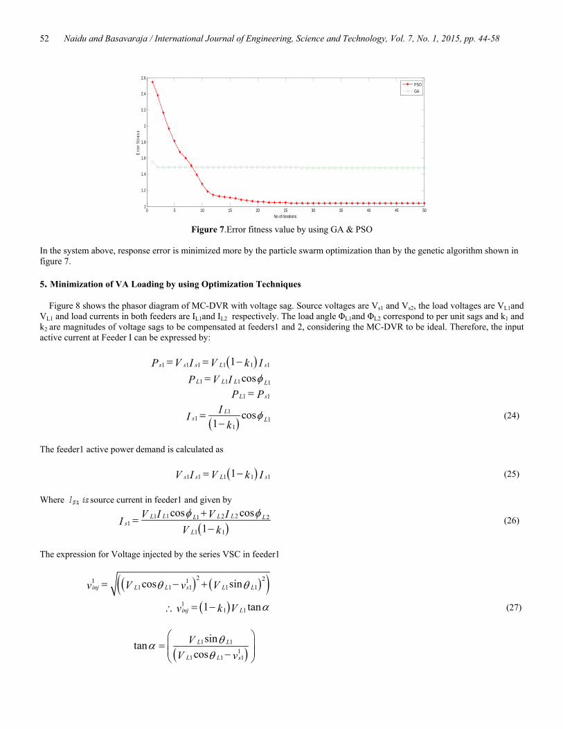
Figure 7.Error fitness value by using GA & PSO
In the system above, response error is minimized more by the particle swarm optimization than by the genetic algorithm shown in figure 7. 5. Minimization of VA Loading by using Optimization Techniques
Figure 8 shows the phasor diagram of MC-DVR with voltage sag. Source voltages are Vs1 and Vs2, the load voltages are VL1and VL1 and load currents in both feeders are IL1and IL2 respectively. The load angle ΦL1and ΦL2 correspond to per unit sags and k1 and k2 are magnitudes of voltage sags to be compensated at feeders1 and 2, considering the MC-DVR to be ideal. Therefore, the input active current at Feeder I can be expressed by: ( )1 1 11 1 11s s ss LV V kP I I= = −
1 11 1cosL LL LVP I φ= 1 1L sP P=
( )
11 1
1
cos1
Ls L
IIk
φ=−
(24)
The feeder1 active power demand is calculated as ( )1 11 1 11s ss LV V kI I= − (25) Where source current in feeder1 and given by
( )
1 21 21 21
1 1
cos cos1
L LL LL Ls
L
V VI IIV kφ φ+
=−
(26)
The expression for Voltage injected by the series VSC in feeder1
( ) ( )( )2 21 11 1 1 1 1cos sininj L L s L Lv V v Vθ θ= − +
( )11 11 taninj Lv k V α= −∴ (27)
( )1 1
11 1 1
sintancos
L L
L L s
VV v
θαθ
= −
Naidu and Basavaraja / International Journal of Engineering, Science and Technology, Vol. 7, No. 1, 2015, pp. 44-58
53
Figure 8. Phasor diagram of the MC-DVR with voltage sag.
( )1
1 11 taninj Lv k V α= −∴ (28) Hence series VSC power rating is
( ) ( )1 21 21 2
1 1 11 1
cos cos1 tan1
L LL LL Lse L
L
V VI IS k VV kφ φα
+= − −
(29)
Hence power rating of the series VSC in feeder2 can be obtained, by almost equating feeder2 injected voltage to the 2k 2LV (where 2k =1). Therefore the expression for series –VSC power rating in feeder2 is 2 2 2se L sIS V= (30)
By adding equ (29) and (30), the total VA rating of overall MC-DVR can be obtained. 1 2MC DCR se seS S S− = + (31)
The total VA loading of MC-DVR (G. Siva Kumar, 2012) is then the function of 1k , 2k , 1Lφ , 2Lφ , 1Lθ , total harmonic distortions _ 1V LTHD , load currents 1LI , 2LI and rated fundamental voltage 1LV , 2LV . In this function except 1Lθ , all the remaining variables are system dependents. Therefore, the function value i.e., total VA loading of MC-DVR is controlled by varying 1Lθ . This can be expressed as a standard optimization problem as given below ( )1L MC DCRf Sθ −= Where 1Lθ is -90º < 1Lθ < 90º (32)
1Lθ is the control variable with respect to which ( )1Lf θ has to be minimized by using GA and PSO.
6. Results In the proposed analysis, SRF based MC-DVR extensive case study using simulation in sim power system toolbox of MATLAB is done as shown figure.9 and simulation results in parallel distribution power system related to performance of the proposed SRF-Based MC-DVR system as shown. The table 3 shows parameters used in the proposed analysis
Naidu and Basavaraja / International Journal of Engineering, Science and Technology, Vol. 7, No. 1, 2015, pp. 44-58
54
Table 3. System parameters
System Parameters Values System frequency (f) 50HZ
Rated voltage 380V(rms, Phase-Phase) Rs1 andLs1 0.6Ω and 0.1mH Rs2 andLs2 0.6Ω and 0.1mH
Nonlinear Load An Universal bridge consisting of resistor (10) Ω and R-L Load(10Ω and 3mH)
Linear Load-1 A three-phase resistive Load (10) Ω
Linear Load-2 A three-phase R-L Load (10 Ω and 10mH)
VSC-1 and VSC-2 Series T/F (T1andT2)
4kva,200/180,50Hz,10% leakage reactance
Power losses in VSC-1,VSC-2,
Rf1=0.1Ω,Rf2=0.1
Filter capacitors Cf1=10 µF and Cf2=10 µF DC Capacitor(CDC) 2,000µF
Figure 9. Simulink model of multi converter DVR (MC-DVR) in parallel feeder distribution system
A three-phase feeder 1 distribution system has a single phase voltage source designed ( )1 tv with different magnitudes
( 1mv and 2mv ) and has 5thorder harmonics.
( ) 21 1
sin(5 )sin( )5
mm
tvt tv vωω = +
Naidu and Basavaraja / International Journal of Engineering, Science and Technology, Vol. 7, No. 1, 2015, pp. 44-58
55
A three-phase feeder 2 distribution system has a single phase voltage source designed ( )2 tv with different magnitudes ( 1mv
and 2mv ) and has 7thorder harmonics.
( ) 22 1
sin(7 )sin( )7
mm
tvt tv vωω = +
6.1 Voltage sag on both feeders In this case it is assumed that 33% voltage sag occurs on feeder1 & 2 between intervals of time at 0.1sec <t< 0.2sec and at 0.15sec <t< 0.25sec and it is assumed that10% voltage swell occurs on feeder2 between intervals of time at 0.25sec< t <0.3sec, which distorts the load voltages and source voltages in each feeder. Hence we need to regulate the load voltages on both feeders with the help of SRF based MC-DVR controller with optimal PI regulator components. The MC-DVR controller injects the compensated voltage in each feeder to improve load voltages with constant DC-link voltage, as is shown in figure 10 and 11.
Figure 10. The source voltage, injected voltage, load Voltages and DC Capacitor Voltage (VDC) at feeder 1
Figure 11. The source voltage, injected voltage, load Voltages and DC Capacitor Voltage (VDC) at feeder 2
6.2 Three phase fault (LLLG) occurs in feeder2 In this case it is assumed that the three phase fault (LLLG) occurs at feeder 2 in interval of time at 0.3sec<t<0.4sec then healthy feeder1 inject the active power to fault feeder2 through the DC link. Hence the Series VSC 2 injected compensation voltage, and finally regulates the load L2 voltage as shown in figure 12.
Naidu and Basavaraja / International Journal of Engineering, Science and Technology, Vol. 7, No. 1, 2015, pp. 44-58
56
Figure 12. The phase bus voltage, injected voltage, load Voltages and DC Capacitor Voltage (VDC) at feeder 2
6.3 Sudden load changes occur at feeder1 In this case it is assumed that sudden load changes occur at feeder 1 in the interval 0.3s<t<0.4s which has 5thorder harmonic content of 35.04%. In feeder1 DC link voltage decrease due to sudden load change now the Series VSC 1 injects compensated voltage which restores the DC-link voltage to normal value. The analysis are shown in figure 13.
Figure. 12. The phase bus voltage, injected voltage, load Voltages and DC Capacitor Voltage (VDC) at feeder 1
By implementing proposed methodology of SRF-MC-DVR the above analysis shows that the _ 1V LTHD is brought down from 35.04% to 5% at feeder1 and the _ 2V LTHD is brought down from 31.2% to 7% at feeder2, which within the permissible limits. 6.4 minimization of VA Loading by using GA and PSO To minimize the VA loading optimum angle ( 1Lθ ) for voltage injection is found by implementing GA and PSO techniques which results in minimum total VA loading. The optimum angle 1Lθ , injv and phase jump angle α angle can be calculated using equation (32). It is assumed that voltage sag occurs at only feeder1, the per unit value of sag k1 where k1 is 0.6 with the given system parameters the total VA loading of MC-DVR is expressed as a function of 1Lθ are shown in equation (32). Using the GA and PSO technique, the above function shown in equation (32) is optimized with 1Lθ as the variable. The minimum VA loading
Naidu and Basavaraja / International Journal of Engineering, Science and Technology, Vol. 7, No. 1, 2015, pp. 44-58
57
of MC-DVR is obtained which is shown in table. 4 and analysis in figure 14(a) and 14(b), shows the global best (VA Loading) value and variation of fitness function with respect to numbers of iterations.
0 20 40 60 80 100 120 140 160 180 200.4
0.42
0.44
0.46
0.48
0.5
0.52
0.54
No of iterations
G b
est
PSO
GA
Figure 14(a) Global best vs No.of. Iterations Figure 14(b) fitness function vs No.of. Iterations
Table 4. Optimization inject angle and VA loading
Minimization function ( )1Lf θ
VA Loading
(P.U)
1Lθ (degree)
injv (P.U)
Angle of injection α (degree)
By using PSO 0.4001 8.68 0.151 20.68 By using GA 0.4378 2.36 0.2029 26.89
Minimization of VA loading and minimum phase jump angle of the MC-DVR are obtained more by using the PSO than by using GA. 7. Conclusions This paper has discussed design of optimized PI regulator components (Kp and KI) and minimizing the steady state error of the voltage control loop in synchronous-reference- frame (SRF) based MC-DVR controller in three phase systems by using optimization techniques. The proposed controller improves the load voltage in adjacent parallel feeders. From the simulation carried out as described above the following conclusions can be drawn:
• The proposed MC-DVR mitigates the voltage sag from 30% to 0.5% and 5th harmonic distortion is brought down from 35.04% to 5 % at feeder1 and regulates the load voltages in feeder1 with 5% total harmonic distortion.
• It mitigates the voltage swell from 10% to 0.5% and 7th harmonic distortion is brought down from 31.2% to 7 % at feeder2 and regulates the load voltages with 7% total harmonic distortion.
• It mitigates the LLLG on feeder2 to normal values and regulates the load voltages in feeder with permissible THD limits • It mitigates the sudden load changes in each feeder with permissible limits and mitigates all kind of power quality
problems in multi feeder distribution systems with minimum real power injection. The modelling of minimization of volt- ampere (VA) loading of MC-DVR is obtained by using the optimization techniques such as genetic algorithim and PSO. On comparison the best optimal injected angle for injection of voltage by GA is 26.89º and by PSO is 20.68º which is optimal. This reduces volt-ampere rating MC-DVR hence reduce cost. Nomenclature
1nvi+ ith dimensions Velocity of particle at (n+1) th iteration
nix Current position in the ith dimension at nth iteration
C1 Acceleration factor related to pbest
C2 Acceleration factor related to gbest
_ 1V LTHD Total harmonic distortion in load voltages at feeder1
α Voltage Injected angle
APF Active Power Filters
0 20 40 60 80 100 120 140 160 180 2000
2
4
6
8
10
12
Fitn
ess
func
tion
Naidu and Basavaraja / International Journal of Engineering, Science and Technology, Vol. 7, No. 1, 2015, pp. 44-58
58
References Aleem S.H.E.A., Zobaa A.F., and Aziz M.M.A., 2012. Optimal C-type passive filter based on minimization of the voltage
harmonic distortion for nonlinear loads” IEEE Transactions on Industrial Electronics, Vol. 59, No. 1, pp. 431-437. Arnold R. 2001. Solutions to power quality problems, Power Engineering Journal, Vol. 15; No. 2, pp: 65-73. Bollen M.H.J., 2003. What is power quality? Electric Power Systems Research, Vol. 66, No. 1, pp. 5-14. Fujita H. and Akagi H., 1998. The unified power quality conditioner: The integration of series and shunt active filter,” IEEE
Transactions on Power Electronics , Vol. 13, no. 2, pp. 315-322. Hamid R.M, Ali Y.V, and H. Mokhtari, 2009. Multiconverter unified power-quality conditioning systems, IEEE Transactions on
Power Delivery, Vol. 24, No. 3, pp. 1679-1686. Hague M. H. 2001. Compensation of distribution system voltage sag by DVR and D-STATCOM, IEEE Porto Power Tech
Conference, Vol. 1, 10th-13th Sept. Aredes M., Heumann K., and Watanabe E. H., 1998. An universal active power line conditioner,” IEEE Trans. Power Del. , Vol.
13, No. 2, pp. 545–551. Jindal A.K., Ghosh A. and Joshi A., 2008. Voltage regulation in parallel distribution feeders using IVOLCON” Proceedings of
IEEE. Jindal A.K., Ghosh A. and Joshi A., 2007. Interline unified power quality conditioner, IEEE Transactions on Power Delivery,
Vol. 22, No. 1, pp. 364-372. Kesler, M., and E. Ozdemir 2011. Synchronous-reference-frame-based control method for UPQC under unbalanced and distorted
load conditions, IEEE Transactions on Industrial Electronics, Vol.58,.No.9, pp.3967-3975. Kinhal V.G., Agarwal P., and Gupta H.O. 2011. Performance investigation of neural-network-based unified power-quality
conditioner. IEEE Transactions on Power Delivery, Vol. 26, No. 1, pp. 431-437. Kolhatkar Y.Y. and Das S.P., 2007. Experimental investigation of a single-phase UPQC with minimum VA loading, IEEE
Transactions on Power Delivery, Vol. 22, No. 1, pp. 373-380. Panda. S, Padhy N.P. 2008. Comparison of particle swarm optimization and genetic algorithm for FACTS-based controller
design", Applied Soft Computing Journal, Vol. 8, No. 4, pp. 1418–1427. Reid W., 1996. Power quality issues-standards and guidelines, IEEE Transactions on Industry Applications, Vol. 32, no. 3, pp.
625–632. Rodríguez P., Pou J., Bergas J., Candela J. I., Burgos R. P., and Boroyevich D., 2007. Decoupled double synchronous reference
frame PLL for power converters control, IEEE Transactions on Power Electronics, Vol. 22, No. 2, pp. 584-592. Saravanan M., Slochanal S.M.R., Venkatesh P., and Abraham J.P.S., 2007. “Application of particle swarm optimization technique
for optimal location of FACTS devices considering cost of installation and system load ability,” Electrical Power System Research, Vol. 77, pp. 276–283.
Sivakumar. G. 2012. "Minimisation of VA loading of UPQC in three-phase four-wire distribution system, International Journal of Power Electronics, Vol. 4, No. 2.
Wang B., Venkataramanan G., and Illindala M., 2006. Operation and control of a dynamic voltage restorer using transformer coupled H-bridge converters, IEEE Transactions on Power Electronics, Vol. 21, No. 4, pp. 1053-1061.
Biographical notes
Mr. Pudi Vasudeva Naidu was born in 1981. He obtained B.Tech (EEE) degree from Bapatla Engineering College, Nagarjuna University in India , M.Tech from JNTUCH in India and He is pursuing Doctrol Program at Nagarjuna University in India. Currenly he is an Assistant Professor at GITAM University. His areas of interest include Power electronics, Power Quality (PQ) and FACTS. Dr. Banakara Basavaraja (M’04 –SM’10) was born in 1970. He obtained B.Tech (EEE) degree from Gulbaraga University in India, M.Tech from Karanatka University in India and Ph.D from National Insistitute of Technology Warangal. He is senior IEEE Member, Executive Member of ISTE and FIE member. Currently he is a Professor of Electrical & Electronics Engineering Department at the University of BDT Engineering College Davanagere, (Visvesvaraya Technological University Belgaum) Karnataka. His areas of interest include Power Electronics, Adjustable Speed Drives (ASD), Power Quality (PQ), High voltage engineering and EMTP applications. Received March 2014 Accepted April 2014 Final acceptance in revised form October 2014