SANDIA REPORT SAND2015-376607 Unlimited Release Printed December 2015 PV Systems Reliability: Final Technical Report Olga Lavrova, Jack Flicker, Jay Johnson, Kenneth Armijo, Sigifredo Gonzalez, Eric Schindelholtz, N. Rob Sorensen, Ben Yang. Prepared by Sandia National Laboratories Albuquerque, New Mexico 87185 and Livermore, California 94550 Sandia National Laboratories is a multi-program laboratory managed and operated by Sandia Corporation, a wholly owned subsidiary of Lockheed Martin Corporation, for the U.S. Department of Energy’s National Nuclear Security Administration under contract DE-AC04-94AL85000. Approved for public release; further dissemination unlimited. SAND2017-0998R
Transcript
SANDIA REPORT SAND2015-376607 Unlimited Release Printed December 2015
PV Systems Reliability: Final Technical Report Olga Lavrova, Jack Flicker, Jay Johnson, Kenneth Armijo, Sigifredo Gonzalez, Eric Schindelholtz, N. Rob Sorensen, Ben Yang. Prepared by Sandia National Laboratories Albuquerque, New Mexico 87185 and Livermore, California 94550 Sandia National Laboratories is a multi-program laboratory managed and operated by Sandia Corporation, a wholly owned subsidiary of Lockheed Martin Corporation, for the U.S. Department of Energy’s National Nuclear Security Administration under contract DE-AC04-94AL85000.
Approved for public release; further dissemination unlimited.
SAND2017-0998R
DOE Agreement No.25801 PV System Reliability
Dr. Olga Lavrova Sandia National Laboratories
Page 2 of 49
FINAL Report
Project Title: PV System Reliability Project Period: 10/01/13-09/30/15 Budget Period: 10/01/13-09/30/15 Reporting Period: 10/01/13-09/30/15 Reporting Frequency: FINAL Submission Date: 12/30/15 Recipient: Sandia National Laboratories Address: PO Box 5700 Albuquerque, NM 87105 Website (if available) www.sandia.gov Award Number: DE-EE029091 Project Team: Sandia National Laboratories Principal Investigator: Olga Lavrova, Principal Member of the Technical Staff
DOE Project Officer: Holly Thomas DOE Tech Manager: Guohui Yuan _________________________ _____________ Signature Date
DOE Agreement No.25801 PV System Reliability
Dr. Olga Lavrova Sandia National Laboratories
Page 3 of 49
Project Objective:
The continued exponential growth of photovoltaic technologies paves a path to a solar-powered world, but requires continued progress toward low-cost, high-reliability, high-performance photovoltaic (PV) systems. High reliability is an essential element in achieving low-cost solar electricity by reducing operation and maintenance (O&M) costs and extending system lifetime and availability, but these attributes are difficult to verify at the time of installation. Utilities, financiers, homeowners, and planners are demanding this information in order to evaluate their financial risk as a prerequisite to large investments. Reliability research and development (R&D) is needed to build market confidence by improving product reliability and by improving predictions of system availability, O&M cost, and lifetime. This project is focused on understanding, predicting, and improving the reliability of PV systems. The two areas being pursued include PV arc-fault and ground fault issues, and inverter reliability. PV arc-faults and ground faults have caused hundreds of fires in the U.S. and around the world [1]. In cases of faults on rooftop systems, the resulting fire can burn down the building and put the occupants’ lives at risk. In 2011 arc-fault circuit interrupter (AFCI) safety devices were required by the National Electrical Code® [2] on rooftop systems. AFCI products are being listed to the UL 1699B Outline of Investigation, but Standards Technical Panel (STP) experts strongly disagree on which UL requirements should be revised, retained, or modified when converting the UL Outline into a Standard. The STP does agree that the current Outline requires modification because UL-listed AFCIs are experiencing unwanted tripping in the field. Thus, in order to reach a consensus on these topics and convert the Outline of Investigation into a UL Standard, Sandia is performing extensive research into consistent arc-fault generation and nuisance tripping testing. Similarly, the International Electrotechnical Commission (IEC) Technical Committee 82 (TC 82) is creating an arc-fault certification standard and Sandia is collaborating closely with the international group to make the testing procedure realistic for PV installations, establish methods to avoid unwanted tripping, and ensures repeatability of the tests. When an arc-fault or ground fault detector trips in a PV system, no information is provided to the operator about the location of the fault. Determining the location is especially challenging in large PV systems consisting of acres of PV modules. If the problem is not identified quickly, the system operator will continue to lose money and could potentially assume the trip was the result of a nuisance trip and mistakenly turn the system back on. Developing a technology to locate the arc or ground faults will give PV system operators a means to resume operations quickly and minimize the risk that system will restart occurs without repairing the problem. The challenge of locating PV arc and ground faults has been studied by a limited number of researchers [3-6]. The most successful technique is time-domain reflectometry (TDR) in which a step/pulsed voltage signal is sent through the conductors. A short or open circuit condition is manifest as a deviation in the reflected voltage pulse. Open connections (and some types of shorts) occurring in the PV wiring could be found with certain TDR devices [7]. As BOS connectors and solder joints degrade, they become potential locations for arc faults. There are still a number of scientific questions surrounding the degradation process that leads to arc-faults in PV systems. In addition, there is currently no data-driven predictive capability for the degradation of BOS connectors that is built on, and verified by, accelerated tests and field measurements. Such capability has been identified as a critical knowledge gap in the PV industry. While degradation models for solder joints exist, an assessment of the arc fault risk associated with damaged solder joint is necessary to provide context to weakened solder joints.
DOE Agreement No.25801 PV System Reliability
Dr. Olga Lavrova Sandia National Laboratories
Page 4 of 49
Characterization of interconnect degradation has potential for significant O&M applications due to the diagnostic, prognostic, or preventative tools that can be developed with sufficient understanding of the failure mechanisms. In summary, two accomplishments are needed to fully address the arc fault risk of interconnects: 1) Determine a definition of failure based on a risk assessment of arc faults in interconnects; 2) Develop a proven reliability model that can predict the lifetime of interconnects before an arc fault risk is significant. This work addresses two needs in the PV industry: 1) data-driven, predictive capability that informs system operators on the expected rate of degradation for BOS connectors and solder joints; and, 2) an understanding on the effect that this degradation has on series arc-fault risk. Arc-fault damage at these interconnects can cause significant damage but its risk as a function of degradation has not been characterized. Establishing and quantifying the relationship could have significant O&M applications due to the diagnostic, prognostic, and preventative tools that can be developed with a sufficient understanding of the underlying physics and failure mechanisms. If known lifetime estimates are provided and failure precursors are identified, arc-fault detectors could proactively detect a dangerous situation before the fault occurs. Such a shift in operation would be a significant improvement over the current reactive nature of current state-of-the-art arc-fault detectors. One cause of multiple fires is the “blind spot” in the detection area of the GFDI (Ground Fault Detector/Interrupter) protection fuse, which is common in US installations [8, 9]. A GFDI cannot detect a fault on the grounded current-carrying conductor (CCC), which could allow for unrestricted fault current flow bypassing the GFDI if a second fault is initiated in the array. In FY13, Sandia with the SolarABCs steering committee investigated ground faults and the ground fault detection blind spot [8, 9]. The conclusion of this work was that fuse-based GFDI (Ground Fault Detector/Interrupter) designs were vulnerable to faults to the grounded current-carrying conductor. This problem has caused multiple rooftop fires in the past [10]. Sandia and Solar ABCs identified new ground fault detection approaches (isolation monitors, residual current detectors, ground bond current monitors, etc.) [8],but there is little experience with these technologies in the U.S. A team consisting on Sandia, SunPower, and DNV KEMA was established to determine the effectiveness of these new technologies and make recommendations about appropriate thresholds for the detection. If the trip threshold is too low, there will be nuisance trip events; but if the threshold is too high, certain ground faults will go undetected. Proper understanding of detection thresholds maximizes the balance between system performance (uptime), reliability, and safety. As of 2010, the installed cost of PV systems was $3.40/Watt [11]. While most research, both historically and currently, has focused on the production costs of PV module technology, the cost of the necessary grid-connected DC-to-AC inverters has been largely ignored. As the price of PV modules drops, the price of inverters becomes more important. Inverters now constitute 8-12% of the total lifetime PV cost [12]. As of 2010, the inverter and associated power conditioning components accounted for $0.25/Watt [13], well above the DOE benchmark of $0.10/Watt by 2017 [11]. One of the key price drivers of the inverter component is inverter reliability [14, 15]. PV modules have long lifetimes with warranties offered up to 20 years. The mean time between failure (MTBF) of these systems have been shown, in the field, to be up to 522 years for residential and 6,666 years for utility systems [16]. In contrast, the inverter component has shown a field MTBF of between 1 and 16 years [16, 17]. Typical warranties on these devices
DOE Agreement No.25801 PV System Reliability
Dr. Olga Lavrova Sandia National Laboratories
Page 5 of 49
last only five to ten years [15], with a few manufacturers offering extended warranties for purchase up to 15 years. Even with the most optimistic view of inverter lifetime, it will be necessary to replace or repair an inverter multiple times over the lifetime of a PV module. Repairing the inverter is costly not only due to replacement parts and work crews, but also incidental costs, such as the loss of power not generated during downtime, purchasing replacement power unsupplied by the offline system, and any performance degradation before failure identification [15]. Inverter issues are especially problematic since, depending on the PV topology, they may affect the power production of a large number of modules and/or strings. According to SunEdison, a North American-based PV plant operator with over 750 PV plants across the world, inverter performance was responsible for 36% of total energy losses between January 2010 and March 2012 [18]. The inverter is less reliable than other components in the PV system because it is a complicated switching/monitoring system with a number of responsibilities. The main purpose of an inverter is to output power meeting power quality standards (e.g., IEEE 1547 [19] in North America or IEC61727 [20] in Europe). However, depending on the local/national ordinances or complexity of the device, the inverter may also be required to manage power output of the PV module, connect/disconnect from the grid, manage var, read and report status, or monitor islanding [12]. Added inverter functionalities exponentially increase the difficulty in creating both reliable and affordable components. In addition to having a number of functionalities, the inverter must also operate in relatively harsh, changing environments. Inverters may experience large temperature swings from -30 to 70⁰C, humidity conditions from 0 to 100%, and/or salty, corrosive environments. PV inverters are responsible for most of the reliability issues in the solar energy system [15]. Among different components in a PV inverter, power semiconductor devices and soldering failure are responsible for more than 20% of all failures [21]. Die-attachment degradation is the most common type of failure mechanism in switches and will result in an increase in on-state resistance of MOSFETs during its natural aging process [22]. Thus, the ON-resistance, Rds (on), is considered as an indicator of MOSFET aging [23]. Several techniques have been proposed to estimate the life of PV inverters based on their circuit structures. The authors of [15] suggested a model framework to decompose the inverter into subsystems, and different circuit topologies have been evaluated to decide the reliability in [24] and [25], respectively. For these two methods mentioned above, it is extremely difficult to forecast a failure before it occurs which limits their applications in condition monitoring of PV inverters. To overcome this shortcoming, additional probes, hardware circuits as well as digital controllers are being added to inverters in order to monitor the operation status of power devices [26]. Although the real-time condition of power devices can be successfully decided by using these extra components, it is not a cost-effective solution. In short, inverters must fulfill a complicated and ever expanding power handling role in harsh environments while still meeting the extremely cost-sensitive needs of the PV economic environment. In the future, inverter technology cost must decrease by 50%, with a 2X increase in reliability to facilitate grid parity of solar energy in the future [15, 27].
DOE Agreement No.25801 PV System Reliability
Dr. Olga Lavrova Sandia National Laboratories
Page 6 of 49
Simulation of modern inverter sub-systems and power electronics is an attractive performance and reliability tool due to its ease, flexibility, and cost compared to experimental methods. However, power electronics simulations have always been a challenge due to the non-linear behavior or power switches, connection to continuous sub-systems, and design of discrete-time control. Recent changes in inverter circuit topologies and switching schemes have made simulation scalability, modularity and optimization more challenging and time-intensive [28]. A realistic mission profile normally includes millions of switching events [28], making compact models [29, 30] (though accurate) very slow and not necessarily scalable. Task 1: Provide Technical Guidance to UL, IEC, and NEC to Improve Codes and
Standards
Task Objective: Provide Technical Guidance to UL, IEC, and NEC to Improve Codes and Standards To improve fire safety in PV systems, the 2014 National Electric Code (NEC) requires arc-fault protection on all PV systems [31]. Arc-fault circuit interrupters (AFCI) meet this requirement by containing an arc-fault detector (AFD), which identifies an arc-fault and circuit interrupter, which de-energizes the PV system. In order to create robust arc-fault detection algorithms, tests must be completed on a range of PV systems: the algorithm must not nuisance trip on different inverter noise signatures, while also detecting arcing within the times prescribed in the UL 1699B requirement [32]. Additionally, AFD certification testing is permitted on real PV systems and on PV simulators since testing could be stopped for weeks or months in cloudy areas (e.g., Germany). PV simulators induce noise on the DC system because they are switching devices and this can cause unwanted tripping of the AFD. This leads to questions about the validity of the test procedure. Sandia investigated the validity of testing AFDs on PV simulators to provide results to the UL STP committee for considering the revision of the UL 1699B draft. Creating a consensus-based certification and safety standards for arc-fault circuit interrupters (AFCIs), arc-fault detectors (AFDs) will ensure faults are successfully detected and de-energized. For this investigation, to accelerate robust AFD algorithm development, Sandia National Laboratories collected noise signatures from different arc-faults, inverters and combiner boxes. An example of these types of arc-fault signatures can be seen in Fig. 1. In order to test AFDs at Nationally Recognized Test Laboratories (NRTLs) there is a provision for using PV simulators because real PV may not be practical in some locations. There has been no scientific investigation into the difference of using PV simulators to test arc-fault detectors and because they are switching devices that may cause nuisance tripping (this has happened at DETL multiple times), so the validity of the test may be called into question. Sandia will investigate the difference in real PV and simulated PV when conducting arc-fault detector testing and report the findings to the UL STP. Through this task, Sandia also supported the UL STP, IEC, and NEC CMPs. Task 1 Results
Milestone 1.1: Generate arc-faults on real PV systems and in artificial configurations created by PV simulators. Measure the high frequency current content in the PV system.
DOE Agreement No.25801 PV System Reliability
Dr. Olga Lavrova Sandia National Laboratories
Page 7 of 49
This task has been completed during Q2 FY15. Tests were conducted at a variety of arc power levels, variety of arc start configuration and on a variety of connectors with different materials. Results have been previously summarized and will be re-iterated in the final report.
Figure 1. Second Generation Arc-Fault Generator with adaptable mounts, unified
instrumentation and 600V, 30A power ratings.
Milestone 1.2: Compare the system baseline noise and arc-fault noise signatures from the real PV systems and the artificial PV systems. The Sandia team collaborated with Texas A&M University to investigate novel methodologies for assessing arc-fault signatures, such as the Replay method. This methodology, as presented by McConnel et. al. [33] assesses the FFT signatures of the DC current during operation to evaluate the onset of an arc-fault. This method will enable the detection of real arc discharges using AFDs, while ensuring that nuisance tripping issues do not occur. In addition, collaborators at Texas A&M University have begun to develop novel algorithms, which can utilize the arc-fault signatures obtained at Sandia to determine the onset of a real arc-fault event. Fig. 2 presents a graphical representation of one of the methodologies:
DOE Agreement No.25801 PV System Reliability
Dr. Olga Lavrova Sandia National Laboratories
Page 8 of 49
Figure 2. Novel potential method for arc fault detection algorithm. Milestone 1.3: Provide recommendations to UL 1699B STP and IEC TC 82 on the viability of using PV simulators to perform arc-fault detection testing in UL and IEC standards. The UL 1699B STP has met at the UL Northbrook Office May 19-20, 2015. Jay Johnson presented the results from the last 2 years to the standards technical panel to drive the Outline of Investigation draft toward a consensus testing procedure. UL1699B ballot went to a vote for inclusion as an ANSI standard, however the proposal was voted down. Sandia is continuing to work with the Task UL force to address the issues. TAMU and Sandia have been in detailed discussions with the UL 1699B task group about PV simulators. This work will still continue in Q4. Task 2: Invent novel methods for locating faults in PV systems Task Objective: Develop a tool for determining the location of arc and ground faults on PV systems once arc-fault and ground fault detectors have tripped. Compare this method with other commercial options to evaluate the new tool relative to search accuracy and efficiencies. When an arc-fault or ground fault detector trips in a PV system, no information is provided to the operator about the location of the fault. Determining the location is especially challenging in large PV systems consisting of acres of PV modules. If the problem is not identified quickly, the system operator will continue to lose money and
DOE Agreement No.25801 PV System Reliability
Dr. Olga Lavrova Sandia National Laboratories
Page 9 of 49
could potentially assume the trip was the result of a nuisance trip and mistakenly turn the system back on. Developing a technology to locate the arc or ground faults will give PV system operators a means to resume operations quickly and minimize the risk that system will restart occurs without repairing the problem. The challenge of locating PV arc and ground faults has been studied by a limited number of researchers [42, 43, 44, 45]. It is preferred to remotely determine the location of the fault (as opposed to measuring the system locally for problems) so there has been a lot focus on reflectometry technologies (used for a long time to detect faults in long transmission lines). The most successful technique is time-domain reflectometry (TDR) in which a step/pulsed voltage signal is sent through the conductors. A short or open circuit condition is manifest as a deviation in the reflected voltage pulse [42, 43, 44, 45]. There are also a few commercial devices that can locate certain types of faults on PV systems. For instance, opens caused by series arc-faults can be located with Togami Line-Checkers, although these devices require tracing the electrical path to determine the fault locations. Open connections (and some types of shorts) occurring in the PV wiring could be found with certain other TDR devices [46]. Unfortunately, these devices are not designed for conductive paths with semiconductors or branch circuits, so remote fault finding is not effective in PV systems. It is believed that some of the technical limitations with TDR can overcome with spread spectrum time domain reflectometry (SSTDR) because this technique uses multiple frequencies so harmonics and reflections in connectors can be minimized. Sandia and the University of Utah are collaborating on creating a novel method of determining the location of an arc and ground fault in large PV systems using SSTDR. Task Approach: In certain fault cases, SSTDR data has identified the fault location using the method illustrated in Fig. 3. However, it is far easier to locate an open in the PV system cause by an arc-fault than it is to locate a parallel arc-fault or ground fault. The associated SSTDR electrical connections and analysis must be determined for each of these cases. Two additional barriers will be investigated in the future: effects of large, branched circuits in MW PV systems and methods to avoid creating a “health” scan baseline against which the results are compared. In addition, the SSTDR results will be compared with alternative fault-finding technologies on the market to determine which are most applicable to PV applications.
DOE Agreement No.25801 PV System Reliability
Dr. Olga Lavrova Sandia National Laboratories
Page 10 of 49
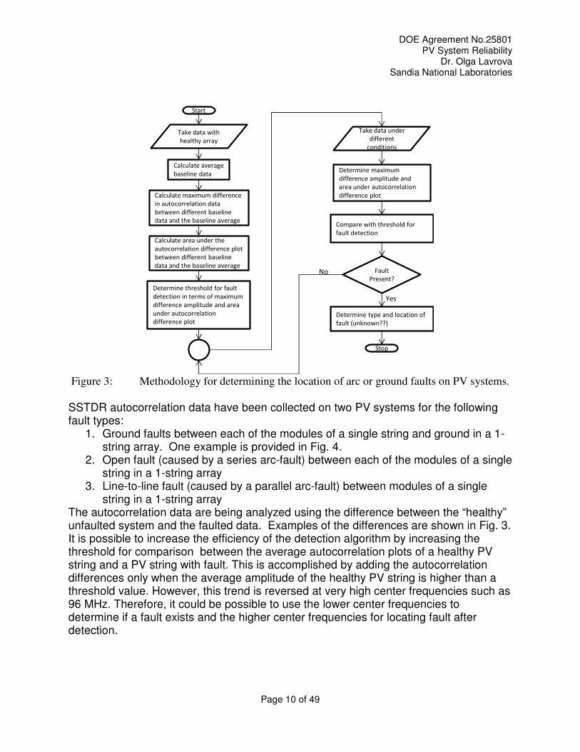
Figure 3: Methodology for determining the location of arc or ground faults on PV systems. SSTDR autocorrelation data have been collected on two PV systems for the following fault types:
1. Ground faults between each of the modules of a single string and ground in a 1-string array. One example is provided in Fig. 4.
2. Open fault (caused by a series arc-fault) between each of the modules of a single string in a 1-string array
3. Line-to-line fault (caused by a parallel arc-fault) between modules of a single string in a 1-string array
The autocorrelation data are being analyzed using the difference between the “healthy” unfaulted system and the faulted data. Examples of the differences are shown in Fig. 3. It is possible to increase the efficiency of the detection algorithm by increasing the threshold for comparison between the average autocorrelation plots of a healthy PV string and a PV string with fault. This is accomplished by adding the autocorrelation differences only when the average amplitude of the healthy PV string is higher than a threshold value. However, this trend is reversed at very high center frequencies such as 96 MHz. Therefore, it could be possible to use the lower center frequencies to determine if a fault exists and the higher center frequencies for locating fault after detection.
Start
Take data with
healthy array
Calculate average
baseline data
Calculate maximum difference
in autocorrelation data
between different baseline
data and the baseline average
Calculate area under the
autocorrelation difference plot
between different baseline
data and the baseline average
Determine threshold for fault
detection in terms of maximum
difference amplitude and area
under autocorrelation
difference plot
Take data under
different
conditions
Determine maximum
difference amplitude and
area under autocorrelation
difference plot
Compare with threshold for
fault detection
Fault
Present?
Determine type and location of
fault (unknown??)
Stop
No
Yes
DOE Agreement No.25801 PV System Reliability
Dr. Olga Lavrova Sandia National Laboratories
Page 11 of 49
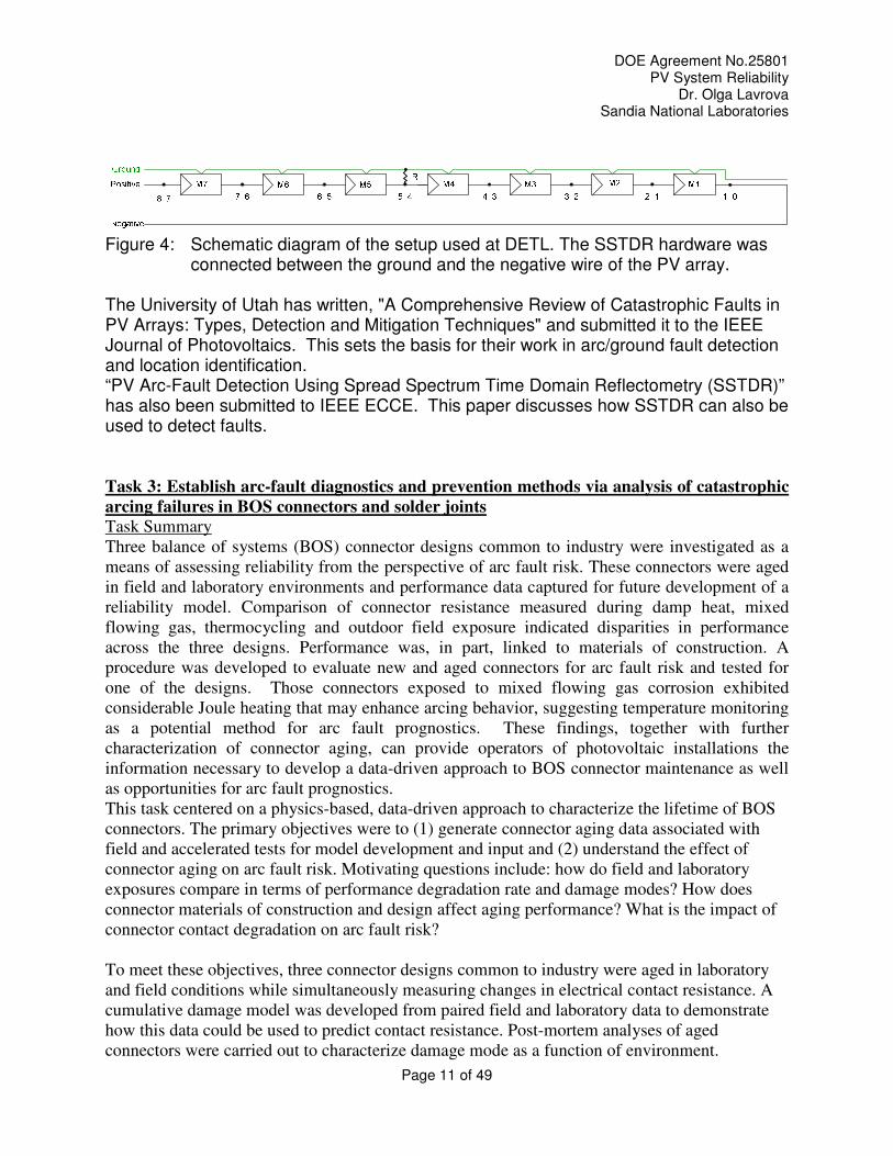
Figure 4: Schematic diagram of the setup used at DETL. The SSTDR hardware was
connected between the ground and the negative wire of the PV array. The University of Utah has written, "A Comprehensive Review of Catastrophic Faults in PV Arrays: Types, Detection and Mitigation Techniques" and submitted it to the IEEE Journal of Photovoltaics. This sets the basis for their work in arc/ground fault detection and location identification. “PV Arc-Fault Detection Using Spread Spectrum Time Domain Reflectometry (SSTDR)” has also been submitted to IEEE ECCE. This paper discusses how SSTDR can also be used to detect faults. Task 3: Establish arc-fault diagnostics and prevention methods via analysis of catastrophic
arcing failures in BOS connectors and solder joints
Task Summary Three balance of systems (BOS) connector designs common to industry were investigated as a means of assessing reliability from the perspective of arc fault risk. These connectors were aged in field and laboratory environments and performance data captured for future development of a reliability model. Comparison of connector resistance measured during damp heat, mixed flowing gas, thermocycling and outdoor field exposure indicated disparities in performance across the three designs. Performance was, in part, linked to materials of construction. A procedure was developed to evaluate new and aged connectors for arc fault risk and tested for one of the designs. Those connectors exposed to mixed flowing gas corrosion exhibited considerable Joule heating that may enhance arcing behavior, suggesting temperature monitoring as a potential method for arc fault prognostics. These findings, together with further characterization of connector aging, can provide operators of photovoltaic installations the information necessary to develop a data-driven approach to BOS connector maintenance as well as opportunities for arc fault prognostics. This task centered on a physics-based, data-driven approach to characterize the lifetime of BOS connectors. The primary objectives were to (1) generate connector aging data associated with field and accelerated tests for model development and input and (2) understand the effect of connector aging on arc fault risk. Motivating questions include: how do field and laboratory exposures compare in terms of performance degradation rate and damage modes? How does connector materials of construction and design affect aging performance? What is the impact of connector contact degradation on arc fault risk? To meet these objectives, three connector designs common to industry were aged in laboratory and field conditions while simultaneously measuring changes in electrical contact resistance. A cumulative damage model was developed from paired field and laboratory data to demonstrate how this data could be used to predict contact resistance. Post-mortem analyses of aged connectors were carried out to characterize damage mode as a function of environment.
DOE Agreement No.25801 PV System Reliability
Dr. Olga Lavrova Sandia National Laboratories
Page 12 of 49
Furthermore, arc fault risk of new and aged connectors was assessed via a novel experimental platform and test methodology developed for this program. The following is a summary of this work. Task Methods A. Aging Tests
Four exposure environments were chosen to characterize the effects of various environmental stress factors on electrical contact resistance and materials degradation. Three common latching BOS connector designs, from three different manufacturers, were exposed in these environments. Two of these exposures were comprised of laboratory accelerated tests commonly used for robustness screening of photovoltaic components and electrical contacts- mixed flowing gas (MFG) and damp heat. The damp heat test was conducted using conditions stated in IEC60068 for laboratory air at 85o C/85% RH. Grime simulants for coastal and desert environments were applied to a subset of samples exposed to the damp heat to examine the effect of contamination on contact performance. Mixed flowing gas exposure was according to ASTM B845, Method G, which involves exposure to a gas mixture of H2S, Cl2, NO2 at ppb levels, 70% RH and 30 oC. This test has been demonstrated to emulate and accelerate damage of in- service electrical contacts in sheltered light industrial atmospheric conditions. The third laboratory exposure consisted of temperature cycling of as-received and MFG-aged connectors between -40 °C and 100 °C at a ramp rate of 10 °C·min-1 between these points. This ∆T range is between 5 and 10 °C outside of the min and max average manufacturer-stated temperature specs of the three connector types. The fourth exposure was carried out at an outdoor test site at Sandia National Labs in Albuquerque, which can be classified as a light industrial, high desert environment. Connectors were mounted on a boldly exposed polycarbonate panel at 45° relative to the ground and facing south. Four-wire resistance measurements were made across the connectors on an hourly basis during all tests using calibrated and multiplexed milliohm meters, Figure 5.
B. Materials Analysis
Both as-received and aged connector pins and sockets were cross-sectioned and examined using optical and electron microscopy. Regarding the latter, analysis was performed using a Zeiss Supra 55VP field emission SEM under high vacuum, 20 kV accelerating voltage, and a working distance of 10 mm in both secondary and backscattered electron modes. A Bruker SDD EDS detector and software were utilized for compositional analysis.
Figure 5. Outdoor connector exposure setup at SNL, Albuquerque.
DOE Agreement No.25801 PV System Reliability
Dr. Olga Lavrova Sandia National Laboratories
Page 13 of 49
C. Arc Fault Tests
The arc fault behavior of select as-received and aged connector pins and socket sets was characterized using an arc fault generator described earlier in this report. A PV simulator running a constant power 300W I-V curve was used as the power source. Voltage, current and connector surface temperature were captured at a rate of 2 Hz during these tests using methods. In these experiments, power was run across a set of connectors under test while simultaneously separating a fully mated connector at 0.09 mm/s using a motorized linear stage until a sustained arc occurred. Resistance across the connector pin and socket rises during separation due to a gradual decrease in contact area. If a decreased amount of translation is necessary to produce a sustainable arc, then the resistance increases and the connector disturbance needed to cause an arc-fault event also increases. The separation distance prior to the first detected spark as well as that required for a sustainable arc was examined as a means to infer the relative risk of arcing between contacts in a connector. The intermittent and sustained arcing events were visually observed and position noted during the experiments. The separation velocity utilized was found to provide sufficient time for a sustained arc to develop as a result of separation. Results and Discussion A. Aging Tests
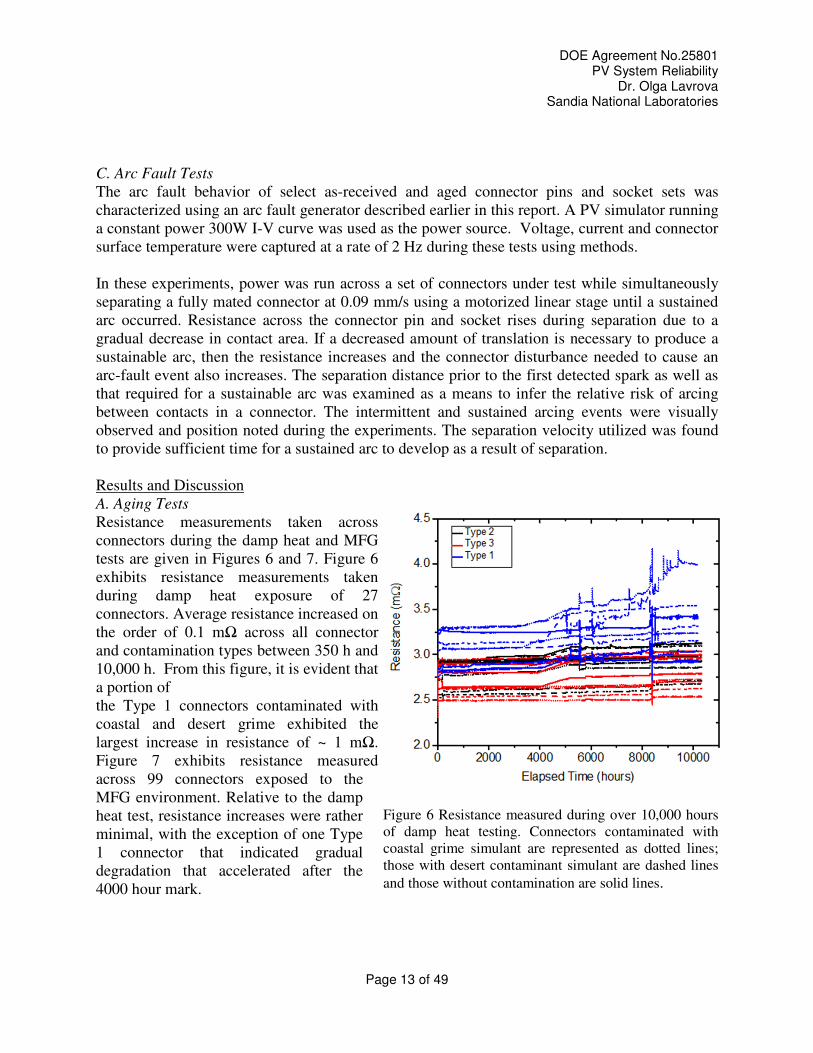
Resistance measurements taken across connectors during the damp heat and MFG tests are given in Figures 6 and 7. Figure 6 exhibits resistance measurements taken during damp heat exposure of 27 connectors. Average resistance increased on the order of 0.1 mΩ across all connector and contamination types between 350 h and 10,000 h. From this figure, it is evident that a portion of the Type 1 connectors contaminated with coastal and desert grime exhibited the largest increase in resistance of ~ 1 mΩ. Figure 7 exhibits resistance measured across 99 connectors exposed to the MFG environment. Relative to the damp heat test, resistance increases were rather minimal, with the exception of one Type 1 connector that indicated gradual degradation that accelerated after the 4000 hour mark.
Figure 6 Resistance measured during over 10,000 hours of damp heat testing. Connectors contaminated with coastal grime simulant are represented as dotted lines; those with desert contaminant simulant are dashed lines
and those without contamination are solid lines.
DOE Agreement No.25801 PV System Reliability
Dr. Olga Lavrova Sandia National Laboratories
Page 14 of 49
Temperature cycling for 100 connectors was carried out for 610 cycles. The results for 25 as-received Type 2 connectors are given in Figure 8. A comparison between room temperature resistance measured prior to cycling and room temperature resistance during a pause in cycling (1080 hours) indicates an average resistance increase of 7 mΩ. One connector, not included in this statistic, exhibited increasingly frequent intermittent resistance between near baseline and near 10 Ω, as seen with a number of the outdoor exposed Type 2 connectors. The average increase in resistance is approximately an order of magnitude greater than that exhibited by 10,000 hours of damp heat exposure and 5000 hours of mixed flowing gas exposure (~ 1 mΩ). The results for 1.5 years of outdoor exposure of 55 connectors are given in Figure 9. Noise in the data is due to diurnal and seasonal temperature variance. Comparison of average resistance measurements across all connectors during similar temperature regimes (2000 and 10,000 hours) indicated that values increased on the order of 1 mΩ, excluding one Type 3 connector and nine Type 2 connectors. These connectors exceptionally exhibited the greatest change in resistance, up to 100 mΩ, amongst connectors across all three laboratory exposure tests. Comparison between the different environments shows that, with the exception of thermal cycling, outdoor exposure generally invoked higher resistance increases at faster rates than the laboratory tests. Temperature variance is one of the major environmental stressor differences between the outdoor test and MFG and damp heat tests. Given this and the fact that thermal cycling was able to invoke higher contact resistance increase rates, it appears that thermal
Figure 7 Resistance measured across 99 connectors in a MFG corrosion chamber over the course of 5000 hours. Corrosion-induced degradation of one connector out of the sample is readily visible.
DOE Agreement No.25801 PV System Reliability
Dr. Olga Lavrova Sandia National Laboratories
Page 15 of 49
variance is a primary driver for contact resistance increase. There are a number of potential degradation modes related to thermal cycling that could be responsible for resistance increase, including fretting and corrosion of the corrosion due to differential thermal expansion and contraction of the materials. A linear cumulative damage model was developed from paired field and thermal cycling data to demonstrate how field and laboratory accelerated tests could be used to predict contact resistance. Specifically, the data was fit to the Coffin-Manson model:
LL
∆T∆T
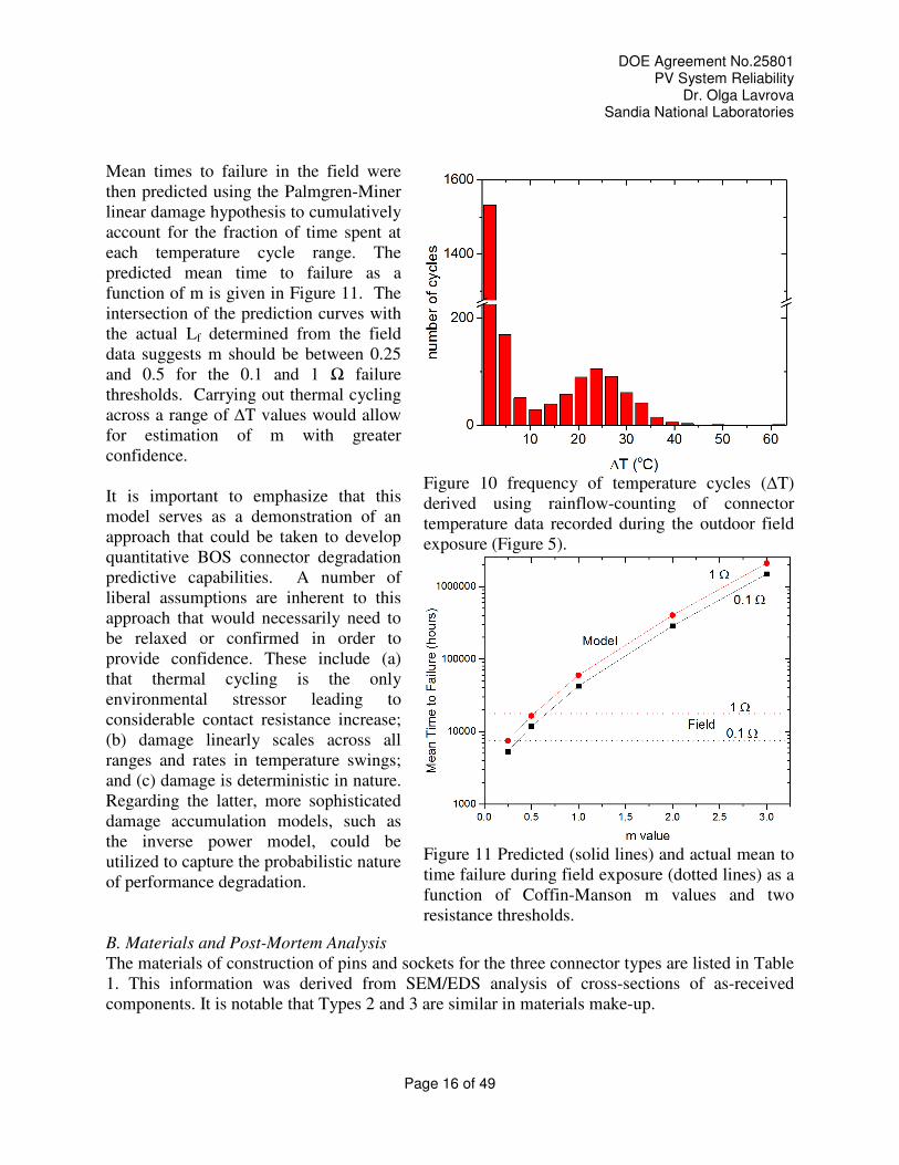
Where Lf is the time to failure in the field; Lt is the time to failure in the lab test; ∆Tt is the range of temperature swing in the lab test and ∆Tf is the range in the field; and m is an experimental constant. For the laboratory thermal cycling test, ∆Tt = 140 °C and Lf was determined as the mean time to failure for those connectors that exceeded an arbitrarily chosen increase in resistance of 0.1 or 1 Ω. Major temperature cycles witnessed during the field exposure were characterized using a rainflow-counting algorithm. Lf was subsequently determined for each of the temperature cycle ranges (∆Tf) in Figure 10, assuming m values from 0.25 to 3.
Figure 8 Resistance measured across 25 new, as-received Type 2 connectors during laboratory thermal cycling.
Figure 9 Resistance (upper) and temperature (lower) measured on connectors boldly exposed to 1.5 years of a high-desert light industrial outdoor environment.
DOE Agreement No.25801 PV System Reliability
Dr. Olga Lavrova Sandia National Laboratories
Page 16 of 49
Mean times to failure in the field were then predicted using the Palmgren-Miner linear damage hypothesis to cumulatively account for the fraction of time spent at each temperature cycle range. The predicted mean time to failure as a function of m is given in Figure 11. The intersection of the prediction curves with the actual Lf determined from the field data suggests m should be between 0.25 and 0.5 for the 0.1 and 1 Ω failure thresholds. Carrying out thermal cycling across a range of ∆T values would allow for estimation of m with greater confidence. It is important to emphasize that this model serves as a demonstration of an approach that could be taken to develop quantitative BOS connector degradation predictive capabilities. A number of liberal assumptions are inherent to this approach that would necessarily need to be relaxed or confirmed in order to provide confidence. These include (a) that thermal cycling is the only environmental stressor leading to considerable contact resistance increase; (b) damage linearly scales across all ranges and rates in temperature swings; and (c) damage is deterministic in nature. Regarding the latter, more sophisticated damage accumulation models, such as the inverse power model, could be utilized to capture the probabilistic nature of performance degradation. B. Materials and Post-Mortem Analysis
The materials of construction of pins and sockets for the three connector types are listed in Table 1. This information was derived from SEM/EDS analysis of cross-sections of as-received components. It is notable that Types 2 and 3 are similar in materials make-up.
Figure 10 frequency of temperature cycles (∆T) derived using rainflow-counting of connector temperature data recorded during the outdoor field exposure (Figure 5).
Figure 11 Predicted (solid lines) and actual mean to time failure during field exposure (dotted lines) as a function of Coffin-Manson m values and two resistance thresholds.
DOE Agreement No.25801 PV System Reliability
Dr. Olga Lavrova Sandia National Laboratories
Page 17 of 49
Table 1 Material Construction of Connector Types under Study
Type Base Alloy Underplate, Nominal
Thickness (µm)
Overlayer, Nominal
Thickness (µm)
I Cu-Zn-Pb Cu, 1 Ag, 3-4
II Cu -- Sn, < 1 -8
III Cu Ni, 1 Sn, 5-9
Post-mortem analysis was carried out on connector pins that were boldly exposed (no housing) to the MFG environment to ascertain extent of corrosion damage. In general, the tin-plated Type 2 and 3 connectors qualitatively suffered less corrosion than the silver-plated Type 1 connectors. Micrographs in Figure 12 exemplify this. Type 2 and 3 connectors exhibited sparse and localized attack of the underlying base metal in areas of thinner plating or porosity, as exemplified in Figure 8c. This is in contrast to the relatively uniform and nearly complete mineralization of the silver plating (a) and attack of underlying base metal (b) of the Type 1 connectors. The thickness of the mineralized silver layer on one cross-section averaged 7 ± 4 µm.
The disparity in performance across the three connector types is attributed to variance in corrosion response related to materials of construction, Table 1. In contrast to the minimal corrosion seen on the tin-plated Type 2 and 3 connector pins when boldly exposed without their housing, the boldly exposed Type 1 pins exhibited severe corrosion, Figure 8. Relative to tin, silver is vulnerable to corrosion in sulfur-rich environments representative of the MFG test and industrial atmospheres, so this could be expected. The results of these tests suggest that if the housing of the Type 1 connecters, which presumably shielded the contacts from the corrosive MFG atmosphere, were to be compromised in a sulfur-rich atmosphere for an appropriate amount of time, corrosion-induced joule heating could lead to arc fault conditions. Post-mortem
Figure 12 SEM image of type II connector contact surface. The magnified inset image shows localized corrosion attack (c) of an area that had minimal plating (bright layer). Left Panel- SEM image of Type I connector contact surface. The magnified inset image shows the mineralized plated Ag layer (a) delaminated from the base metal (b), which is a potential vulnerability leading to arc fault generation. Right Panel-
DOE Agreement No.25801 PV System Reliability
Dr. Olga Lavrova Sandia National Laboratories
Page 18 of 49
analyses similar to those carried out for the MFG tests are necessary to relate the resistance trends in the damp heat tests to the realized degradation of the electrical contacts. Post-mortem analyses of connectors exposed of connectors exposed to damp heat, thermal-cycling, and outdoor exposure were not carried out due to time and resource constraints, but would provide valuable information with regard to damage pathways. Comparison of field and lab exposed connectors would elucidate the degree to which the lab exposures were able to replicate field data. For example, evidence of fretting or fretting corrosion, common electrical contact degradation modes associated with differential thermal expansion and contraction, on outdoor and thermal cycled connectors would provide basis for utilization of thermal cycling as a laboratory accelerated test. Arc Fault Tests
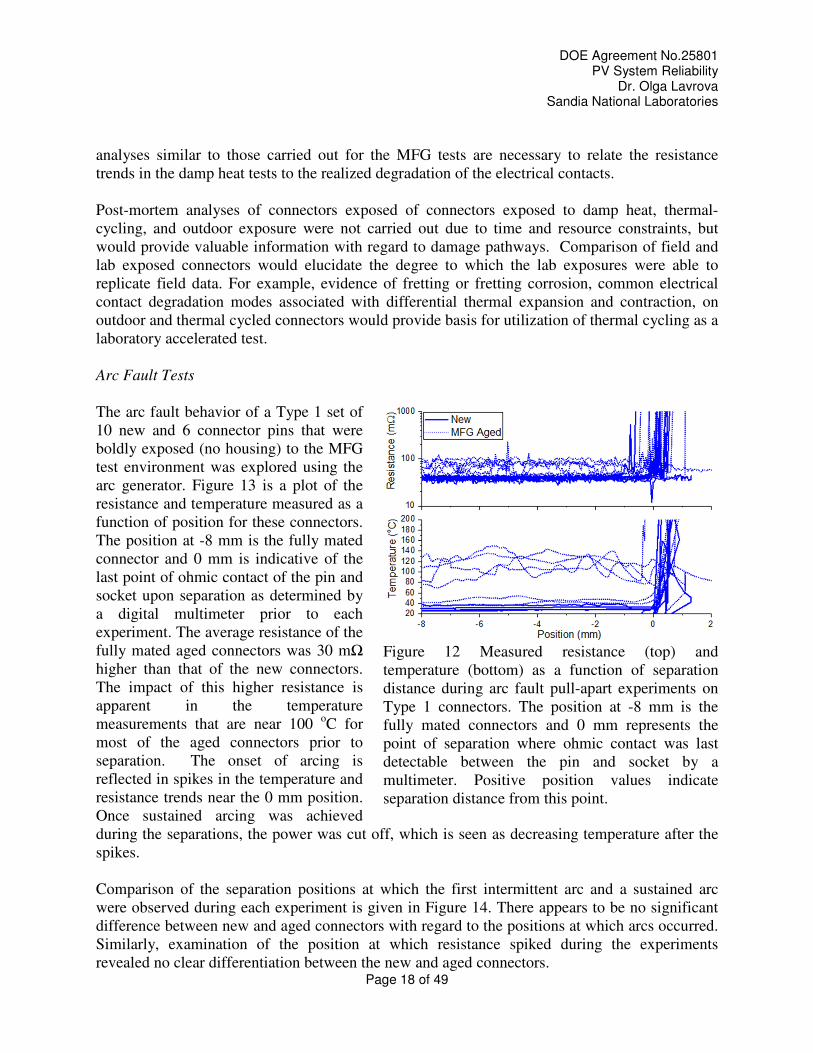
The arc fault behavior of a Type 1 set of 10 new and 6 connector pins that were boldly exposed (no housing) to the MFG test environment was explored using the arc generator. Figure 13 is a plot of the resistance and temperature measured as a function of position for these connectors. The position at -8 mm is the fully mated connector and 0 mm is indicative of the last point of ohmic contact of the pin and socket upon separation as determined by a digital multimeter prior to each experiment. The average resistance of the fully mated aged connectors was 30 mΩ higher than that of the new connectors. The impact of this higher resistance is apparent in the temperature measurements that are near 100 oC for most of the aged connectors prior to separation. The onset of arcing is reflected in spikes in the temperature and resistance trends near the 0 mm position. Once sustained arcing was achieved during the separations, the power was cut off, which is seen as decreasing temperature after the spikes. Comparison of the separation positions at which the first intermittent arc and a sustained arc were observed during each experiment is given in Figure 14. There appears to be no significant difference between new and aged connectors with regard to the positions at which arcs occurred. Similarly, examination of the position at which resistance spiked during the experiments revealed no clear differentiation between the new and aged connectors.
Figure 12 Measured resistance (top) and temperature (bottom) as a function of separation distance during arc fault pull-apart experiments on Type 1 connectors. The position at -8 mm is the fully mated connectors and 0 mm represents the point of separation where ohmic contact was last detectable between the pin and socket by a multimeter. Positive position values indicate separation distance from this point.
DOE Agreement No.25801 PV System Reliability
Dr. Olga Lavrova Sandia National Laboratories
Page 19 of 49
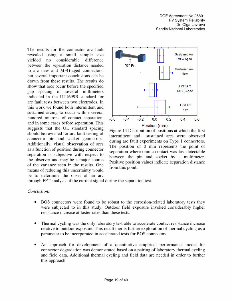
The results for the connector arc fault revealed using a small sample size yielded no considerable difference between the separation distance needed to arc new and MFG-aged connectors, but several important conclusions can be drawn from these results. The results do show that arcs occur before the specified gap spacing of several millimeters indicated in the UL1699B standard for arc fault tests between two electrodes. In this work we found both intermittent and sustained arcing to occur within several hundred microns of contact separation, and in some cases before separation. This suggests that the UL standard spacing should be revisited for arc fault testing of connector pin and socket geometries. Additionally, visual observation of arcs as a function of position during connector separation is subjective with respect to the observer and may be a major source of the variance seen in the results. One means of reducing this uncertainty would be to determine the onset of an arc through FFT analysis of the current signal during the separation test. Conclusions
• BOS connectors were found to be robust to the corrosion-related laboratory tests they were subjected to in this study. Outdoor field exposure invoked considerably higher resistance increase at faster rates than these tests.
• Thermal cycling was the only laboratory test able to accelerate contact resistance increase relative to outdoor exposure. This result merits further exploration of thermal cycling as a parameter to be incorporated in accelerated tests for BOS connectors.
• An approach for development of a quantitative empirical performance model for connector degradation was demonstrated based on a pairing of laboratory thermal cycling and field data. Additional thermal cycling and field data are needed in order to further this approach.
Figure 14 Distribution of positions at which the first intermittent and sustained arcs were observed during arc fault experiments on Type 1 connectors. The position of 0 mm represents the point of separation where ohmic contact was last detectable between the pin and socket by a multimeter. Positive position values indicate separation distance from this point.
DOE Agreement No.25801 PV System Reliability
Dr. Olga Lavrova Sandia National Laboratories
Page 20 of 49
• Performance disparity across connector designs was linked to materials of construction for the mixed flowing gas corrosion laboratory test via post-mortem analyses of exposed connectors. Similar analyses for the other laboratory tests and field-exposed connectors would provide key information necessary for advancement of accelerated tests that invoke damage pathways similar to that of the field environment.
• A procedure to evaluate arc fault risk of new and degraded connectors was tested. The results yielded no discernable difference between the separation distance needed to arc new and mixed flowing gas-aged connector. The results do show that arcs occur before the specified gap spacing of several millimeters indicated in the UL1699B standard for arc fault tests between two electrodes. Suggestions for further improvement of the test methodology were given.
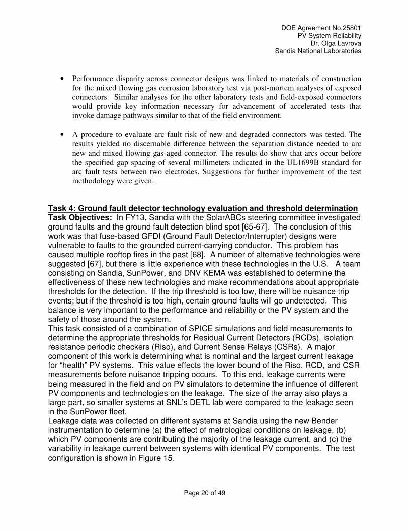
Task 4: Ground fault detector technology evaluation and threshold determination Task Objectives: In FY13, Sandia with the SolarABCs steering committee investigated ground faults and the ground fault detection blind spot [65-67]. The conclusion of this work was that fuse-based GFDI (Ground Fault Detector/Interrupter) designs were vulnerable to faults to the grounded current-carrying conductor. This problem has caused multiple rooftop fires in the past [68]. A number of alternative technologies were suggested [67], but there is little experience with these technologies in the U.S. A team consisting on Sandia, SunPower, and DNV KEMA was established to determine the effectiveness of these new technologies and make recommendations about appropriate thresholds for the detection. If the trip threshold is too low, there will be nuisance trip events; but if the threshold is too high, certain ground faults will go undetected. This balance is very important to the performance and reliability or the PV system and the safety of those around the system. This task consisted of a combination of SPICE simulations and field measurements to determine the appropriate thresholds for Residual Current Detectors (RCDs), isolation resistance periodic checkers (Riso), and Current Sense Relays (CSRs). A major component of this work is determining what is nominal and the largest current leakage for “health” PV systems. This value effects the lower bound of the Riso, RCD, and CSR measurements before nuisance tripping occurs. To this end, leakage currents were being measured in the field and on PV simulators to determine the influence of different PV components and technologies on the leakage. The size of the array also plays a large part, so smaller systems at SNL’s DETL lab were compared to the leakage seen in the SunPower fleet. Leakage data was collected on different systems at Sandia using the new Bender instrumentation to determine (a) the effect of metrological conditions on leakage, (b) which PV components are contributing the majority of the leakage current, and (c) the variability in leakage current between systems with identical PV components. The test configuration is shown in Figure 15.
DOE Agreement No.25801 PV System Reliability
Dr. Olga Lavrova Sandia National Laboratories
Page 21 of 49
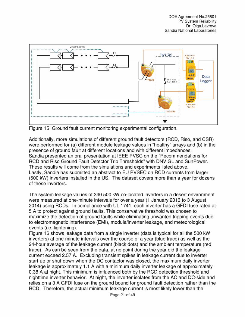
Figure 15: Ground fault current monitoring experimental configuration. Additionally, more simulations of different ground fault detectors (RCD, Riso, and CSR) were performed for (a) different module leakage values in “healthy” arrays and (b) in the presence of ground fault at different locations and with different impedances. Sandia presented an oral presentation at IEEE PVSC on the “Recommendations for RCD and Riso Ground Fault Detector Trip Thresholds” with DNV GL and SunPower. These results will come from the simulations and experiments listed above. Lastly, Sandia has submitted an abstract to EU PVSEC on RCD currents from larger (500 kW) inverters installed in the US. The dataset covers more than a year for dozens of these inverters. The system leakage values of 340 500 kW co-located inverters in a desert environment were measured at one-minute intervals for over a year (1 January 2013 to 3 August 2014) using RCDs. In compliance with UL 1741, each inverter has a GFDI fuse rated at 5 A to protect against ground faults. This conservative threshold was chosen to maximize the detection of ground faults while eliminating unwanted tripping events due to electromagnetic interference (EMI), module/inverter leakage, and meteorological events (i.e. lightening). Figure 16 shows leakage data from a single inverter (data is typical for all the 500 kW inverters) at one-minute intervals over the course of a year (blue trace) as well as the 24-hour average of the leakage current (black dots) and the ambient temperature (red trace). As can be seen from the data, at no point during the year did the leakage current exceed 2.57 A. Excluding transient spikes in leakage current due to inverter start-up or shut-down when the DC contactor was closed, the maximum daily inverter leakage is approximately 1.1 A with a minimum daily inverter leakage of approximately 0.38 A at night. This minimum is influenced both by the RCD detection threshold and nighttime inverter behavior. At night, the inverter isolates from the AC and DC-side and relies on a 3 A GFDI fuse on the ground bound for ground fault detection rather than the RCD. Therefore, the actual minimum leakage current is most likely lower than the
DOE Agreement No.25801 PV System Reliability
Dr. Olga Lavrova Sandia National Laboratories
Page 22 of 49
recorded nighttime RCD current of 0.38 A. These historical RCD values indicate that there is significant overhead in the 5 A UL 1741 GFDI rating and the RCD trip threshold could be reduced to 3 A or less.
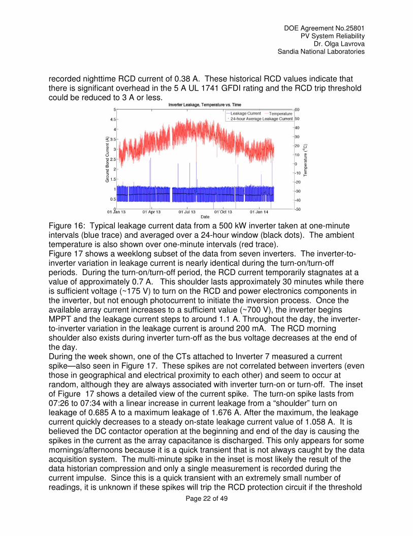
Figure 16: Typical leakage current data from a 500 kW inverter taken at one-minute intervals (blue trace) and averaged over a 24-hour window (black dots). The ambient temperature is also shown over one-minute intervals (red trace). Figure 17 shows a weeklong subset of the data from seven inverters. The inverter-to-inverter variation in leakage current is nearly identical during the turn-on/turn-off periods. During the turn-on/turn-off period, the RCD current temporarily stagnates at a value of approximately 0.7 A. This shoulder lasts approximately 30 minutes while there is sufficient voltage (~175 V) to turn on the RCD and power electronics components in the inverter, but not enough photocurrent to initiate the inversion process. Once the available array current increases to a sufficient value (~700 V), the inverter begins MPPT and the leakage current steps to around 1.1 A. Throughout the day, the inverter-to-inverter variation in the leakage current is around 200 mA. The RCD morning shoulder also exists during inverter turn-off as the bus voltage decreases at the end of the day. During the week shown, one of the CTs attached to Inverter 7 measured a current spike—also seen in Figure 17. These spikes are not correlated between inverters (even those in geographical and electrical proximity to each other) and seem to occur at random, although they are always associated with inverter turn-on or turn-off. The inset of Figure 17 shows a detailed view of the current spike. The turn-on spike lasts from 07:26 to 07:34 with a linear increase in current leakage from a “shoulder” turn on leakage of 0.685 A to a maximum leakage of 1.676 A. After the maximum, the leakage current quickly decreases to a steady on-state leakage current value of 1.058 A. It is believed the DC contactor operation at the beginning and end of the day is causing the spikes in the current as the array capacitance is discharged. This only appears for some mornings/afternoons because it is a quick transient that is not always caught by the data acquisition system. The multi-minute spike in the inset is most likely the result of the data historian compression and only a single measurement is recorded during the current impulse. Since this is a quick transient with an extremely small number of readings, it is unknown if these spikes will trip the RCD protection circuit if the threshold
DOE Agreement No.25801 PV System Reliability
Dr. Olga Lavrova Sandia National Laboratories
Page 23 of 49
is set below the magnitude of the spike. Single, isolated measurements in the data above the 5 A trip threshold do not result in inverter shutdown, so it is unlikely that these transients will cause the RCD to detect the presence of a fault and initiate inverter shut-down. Notably, GFDI fuses intrinsically have resistance to transient events because they are thermally actuated; therefore, as ground fault detection in the U.S. is converted to electrical measurements, it is important to engineer in trip logic robustness with respect to transient currents.
Figure 17: Leakage current data over a week for the seven inverters monitored. A turn-on spike in the leakage current can been seen from Inverter 7 on 29 September 2013 with a close-up view of the spike event shown in the inset.
When describing proper RCD thresholds for ground fault protection, there are three statistical parameters that are of great importance: the average functional leakage of a group of inverters, their standard deviation, and the maximum measured leakage values. The leakage average and standard deviation of a group of inverters is useful for advanced fault detection techniques such as decision tree or outlier detection [13-15]. The maximum leakage values are used for simple thresholding to determine the presence of a fault. Figure 18 (top) shows the raw cumulative distribution functions (CDFs) of all 340 RCDs for one year. Each CDF has a similar multi-tiered shape with a large increase in frequency of measurements at ~0.35 A corresponding to the nighttime baseline of the inverters. A second increase to 50% frequency occurs at ~0.7 A, corresponding to the turn-on/turn-off shoulder leakage. Finally, about 50% of the leakage frequency occurs in the 0.8 to 1.2 A range, corresponding to daytime leakage values. For a given CDF curve, a shift to the right indicates higher leakages in the inverter possibly due to an incorrect baseline value or a high impedance ground fault. A shift up and down typically indicate data drop-outs where the RCD monitor repeats certain values for extended periods of time. Data dropouts and incorrect baseline values contribute to the spread in the CDFs of the inverters. If these effects are corrected (which can be done via simple, on-board programming), such as baselining the inverter leakage each night when the inverter is disconnected and eliminating repeated data due to drop-outs, the CDFs of all 340 inverters are surprisingly tightly distributed (Figure 18 bottom). When inverters are properly baselined and data drop-outs are accounted for, all but five of the 340 inverters
DOE Agreement No.25801 PV System Reliability
Dr. Olga Lavrova Sandia National Laboratories
Page 24 of 49
(colored in blue in Figure 10 bottom) lie within a range of 1.14–1.51 A at 99.99% frequency. The five inverters that act as outliers (CDFs are different colors) demonstrate either higher lower leakage values than average. The RCD values over a six-day period of these outlier inverters along with a “typical inverter” (blue) are shown in the inset. The inverters corresponding to the magenta, green, and black curves show higher measured leakage values during the day while the red curve corresponds to a lower measured leakage value. It should be noted that, although the baseline for each inverter is the same, the turn-off/turn-on shoulder values scale with the daytime leakage of the inverter, indicating that the increased or decreased RCD current may be due to a proportionality (gain) problem in the RCD rather than an actual increase of leakage in the inverter.
The 4σ and 6σ confidence bands of the average CDF of all the inverters (both “normal” and the five outlier inverters) is shown as dashed black lines in (Figure 18 bottom). Note that these curves represent RCD values that are exceeding
rare given the data population: Pr(x ≥ µ+4σ) =
0.00317% and Pr(x ≥ µ+6σ) = 9.87·10-8%. These statistical metrics can be used to establish thresholding rules based on the requirements of the inverter manufacturer, O&M company, plant owner, or standards-
making panel. For example, there is a 4σ confidence that 99.999% of measured
leakage values are below 3.1994 A and a 6σ confidence that 99.999% of the RCD values are below 3.8616 A (Table II). A set point of 5 A (as currently mandated by UL
1741) corresponds to an eight-nines confidence of the 4σ confidence band. For simple thresholding practices, the distribution of leakages for an inverter is of little importance as only the instantaneous leakage value is used to detect the presence of a fault. Therefore, the maximum leakage values of monitored inverters are most important. Figure 19 shows a series of histograms of the measured leakage values of all 340 inverters. At the global level (Figure 19 top), the leakage values cluster into three groups corresponding to the nighttime baseline (~0.32-0.38 A), the turn-on/turn-off shoulder (~0.64-0.72 A), and the daytime leakage (~0.92-1.39 A).
Figure 18: (top) Raw CDFs of inverter leakage for 340 inverters. The CDFs have three distinct sections due to nighttime baseline leakage at ~0.35 A, the turn-on/turn-off shoulder at ~0.7 A, and the daytime leakage at ~1 A. (bottom) CDFs corrected for baseline and data dropouts. Most of the CDFs are clustered together with a few outlier inverters with higher or lower leakages (shown in inset). Assuming a normal distribution,
the +4σ and +6σ limits of the average CDF are shown as black dashed lines.
DOE Agreement No.25801 PV System Reliability
Dr. Olga Lavrova Sandia National Laboratories
Page 25 of 49
Table II: High frequency values of the CDFs for the average of all inverters as well as
the 4σ and 6σ confidence bands. Frequency
(%) Average 4σ4σ4σ4σ 6σ6σ6σ6σ
99 1.1825 2.5067 3.1688
99.9 1.6437 2.9679 3.6300
99.99 1.8028 3.1270 3.7892
99.999 1.8752 3.1994 3.8616
99.9999 2.4891 3.8133 4.4754
99.99999 2.8759 4.2001 4.8623
99.999999 3.6827 5.0069 5.6690
Figure 19: Histogram of baseline and dropout corrected leakage values for 340 inverters. The majority of points are contained in three groups below 2 A (nighttime baseline, turn-on/turn-off shoulder, and daytime leakage). Between 2.5 and 3.75 A, a small number of points were measured, although many of these single measured points can most likely be attributed to noise in RCD measurement.
At higher RCD currents, there is another distribution of values from 1.50-1.82 A (Figure 19 middle) most likely corresponding to the capacitive discharge spikes that occur when the inverter first connects to the array. At even larger currents, there are a small number of points (<10) in the 2.5-4.0 A range (Figure 11 bottom). Due to the large number of data points collected and the compression algorithm of the server, it is assumed that these high current, low frequency data points are noise in the measurement, recording or transient events. This is corroborated by the fact that a
DOE Agreement No.25801 PV System Reliability
Dr. Olga Lavrova Sandia National Laboratories
Page 26 of 49
single leakage value of ~8 A was recorded for one inverter. This single measured RCD current above the trip threshold of 5 A did not cause the inverter to trip due to a ground fault. Therefore, single, high current leakage values are most likely measurement errors that can be safely discounted when determining appropriate trip points for the RCD monitor. As can be determined from the large-scale, long-term data presented here, trip points for the inverter could easily be lowered from 5 A to 3 A with no observable increase in nuisance tripping events.
Task 5: Evaluate and compare arc-fault detectors on the market
Task Objectives: The Sandia National Laboratories PV Arc and Ground Fault Detection and Mitigation
program ran from 2010 until 2015 and made a number of significant contributions to the field of
photovoltaic system safety and reliability. During the course of the program, Sandia worked with over a
dozen solar and original equipment manufacturers and investigated:
• series and parallel arc-fault detection methods;
• improvements to the draft arc-fault circuit interrupter (AFCI) certification standard, UL 1699B;
• arc plasma physics models and burn characteristics;
• array electrical behavior during ground faults (including those constituting the detection ‘blind
spot’); and
• recommendations for novel and traditional ground fault detectors.
A brief summary of the research program and its successes is described below.
The arc-fault research program initially focused on methods of arc-fault detection in DC systems and an
extensive literature review found that DC arc-fault detection could be performed via time-based or
frequency-based methods. While the Sandia team researched the time-domain techniques initially,
frequency-domain methods were found to be more robust and the program focused on this area. By
working with one of the early PV AFCI developers, Eaton Corporation, the team investigated the
conducted arc noise in a number of frequency ranges and discovered that the arc-fault energy was
elevated over the baseline noise most significantly in the 1-100 kHz decades [69]. This discovery, led to a
more thorough investigation of the frequency-dependent filtering characteristics of PV modules and
cables; there was excellent transmission between 1-100 kHz for PV modules [70], but above 100 kHz,
antenna effects, radiative and capacitive coupling, and reflections from impedance mismatches were
present [71]. The team concluded that arc-fault detection at higher frequencies was possible but more
difficult because of unwanted tripping from radio frequency (RF) effects and the 1/f “pink” noise
generated by arc-faults decays at higher frequencies.
AFCI designs were starting to come on to the market to meet the 2011 National Electrical Code (NEC)
690.11 requirement at the end of 2011 [72] Sandia worked to educate the public on the code
requirements and the AFCI development status [73,74]. Sandia also worked directly with a number of
companies to test and improve their AFCI designs [75,76,77] and funded work to investigate more
robust detection algorithms using wavelet decomposition as opposed to the traditional Fourier
transformation methods [78].
DOE Agreement No.25801 PV System Reliability
Dr. Olga Lavrova Sandia National Laboratories
Page 27 of 49
Sandia National Laboratories was also highly active in the development and revisions of the PV AFCI
certification outline of investigation, UL 1699B. Between 2011 and 2015, there were a number open
questions brought up by the UL 1699B Standards Technical Panel that Sandia investigated. Firstly, since
there are nearly limitless combinations of modules, cabling, and power electronics combinations for PV
systems, it was unknown if the few arc-fault detection experiments in the draft certification standard
would ensure the AFCIs work universally. One potential solution was to inject hundreds of pre-recorded
arcing and unfaulted noise signatures into a test circuit to show the AFCI solution was robust to a range
of array hardware, configurations, and topologies—a concept that was used to accelerate the
development of the Sensata Technologies AFCI [79]. A similar idea was to artificially inject arcing noise
into a health PV system at different signal-to-noise ratios to validate or test arc-fault detector algorithm
[80]. Another area of great interest to the UL 1699B STP was determining the arcing energy levels that
caused ignition of polymers because these defined the trip limits for AFCIs. Extensive experimentation
and modeling of arcs in proximity to multiple polymers confirmed the UL 1699B trip times were effective
at preventing fires in PV systems [81]; but, a low power (100 W) test was recommended to be added to
the standard [82]Error! Reference source not found.. For years, the method of generating the arc-fault
(electrode types, geometry, use of steel wool initiator vs. the pull-apart method, etc.) was debated. One
of the primary concerns was that different generation methods produced different noise signals—
elevated noise signals were easy to detect so there could be AFCIs on the market that would not trip on
some arc-faults. AFCI vendors on the other hand argued that the los noise arc-faults were not
representative of field faults. To provide some data to the discussion, Sandia ran hundreds of arc-fault
parametric experiments and compared the noise signatures and found that there was a 20 dB amp
difference in the arc-fault signatures [83], which could easily be the difference between tripping and not
tripping. The discussion within the UL 1699B STP continues today with new electrode geometry
proposal. Lastly, the number and type of UL 1699B tests that should address unwanted tripping was
contentious. Sandia offered suggestions on the type of tests along with the difficulty in passing them by
performing a number of experiments with 10 arc-fault detectors and AFCIs to determine their ability to
withstand unwanted tripping scenarios [84]. There were widespread unwanted tripping failures which
indicated the need to included additional unwanted tripping tests in UL 1699B.
There was strong debate over the expansion of the arc-fault detection requirement to include parallel
arc-faults. Sandia found a number of options for differentiating series and parallel arc-faults [85]Error!
Reference source not found. and submitted a patent on these ideas [86]. Electrical simulations of series
and parallel arc-faults showed that it was possible to detect the fault type through proper
instrumentation [87]. But, ultimately, the requirement for parallel arc-fault detection has not been
included in the NEC because of the low occurrence rate and difficult mitigation method: either shorting
the array or module-level electronics [88].
Locating the arc-fault once the AFCI tripped has been a long standing problem for the industry. It was
determined that the electrical characteristics of the array were not sufficient to determine the fault
location [89]. Alternative methods of locating arc and ground faults were later discussed in a review
paper [90]. One purported advantage of string-level arc-fault detectors was the arc-fault could be easily
located and only a subsection of the array would need to be de-energized. Sandia confirmed this
hypothesis and verified there was a low probability of the arc-fault noise tripping adjacent AFCIs [91]
Sandia also developed a concept of using filters to determine which PV string contained the fault [92]
DOE Agreement No.25801 PV System Reliability
Dr. Olga Lavrova Sandia National Laboratories
Page 28 of 49
Sandia was also interested in understanding and modeling PV failure mechanisms and arc dynamics.
Corrosion of a bypass diode solder joint was shown to generate enough Joule heating that an arc-fault
could be initiated in a junction box [93]. A more thorough investigation of plasma heat transfer was then
performed which confirmed the appropriateness of the UL 1699B trip limits [94]Error! Reference source
not found.. Experimental investigations of connector failure mechanisms via accelerated life testing
were performed to determine the impedance changes with time and estimate the risk of arcing [95].
The life expectancies of AFCIs themselves were also investigated and the burn-in process was found to
be essential for fielded components [96]
Early in the project, it was clear that predicting when an arc-fault was going to happen would be better
than responding to it. “The best arc-fault is one that never happens.” Sandia researched a range of
prognostics and health management (PHM) concepts to find arc-fault ‘canaries’ that could indicate the
PV array was degrading and at risk of experiencing an arc-fault. Some of the methods that were
investigated for arc-fault PHM were impedance spectroscopy [97], impedance increases in solder joints
and connectors [98]Error! Reference source not found., and temperature increases from Joule heating
[99]. The idea of using learning algorithms to detect when PV arrays were experiencing unexpected
degradation was also studied Error! Reference source not found. and a patent was submitted on the
idea.
Ground fault program
Sandia began studying ground-faults, following the revelation that traditional fuse-based Ground-Fault
Detector/Interrupters (GFDIs) were not effective in preventing certain fires – a situation referred to as
the ground fault detection blind spot. Using a high-fidelity SPICE electrical simulation, Sandia discovered
the extent of the problem and found that adjusting the fuse-rating was not effective at solving the
problem.
Working with the Solar America Board for Codes and Standards (Solar ABCs), Sandia identified a number
of alternative ground fault detection technologies that would reduce the fire risk and eliminate the
detection blind spotError! Reference source not found.. These alternatives included isolation monitors
(Riso) that measured the array impedance to ground, current sense monitors (CSMs) that monitor the
ground current in DC-grounded systems, and residual current detectors (RCDs) that measure the
differential current in the DC source circuits, typically at the inverter. Sandia also funded the University
of Utah to research new methods of ground fault detection and location identification using time
domain reflectometry.
The team worked with industry to find the ideal ground fault detection thresholds for each of these
techniques where the largest number of ground faults would be detected without any unwanted
tripping events. RCD measurements from 340 healthy utility-scale inverters were studied for over a year
to determine the distribution of normal RCD measurementsError! Reference source not found.. The
considerations for applying ground fault detection thresholds are numerous: the leakage from the
modules, inverter and other BOS components changes the most sensitive setting before unwanted
tripping occurs, and measurement errors from the environment (e.g., lightning) and are also a challenge.
The thresholds for isolation monitors for CSM and Riso ground fault detectors were derived using
analytical models, but these are highly dependent on the system size, leakage characteristics, and
instrument noise.Sandia proposed that ground fault detectors that have a programmable range of
adjustment so that they can be tuned to the equipment that they are designed to protect.
DOE Agreement No.25801 PV System Reliability
Dr. Olga Lavrova Sandia National Laboratories
Page 29 of 49
Sandia is also working with the UL 62109-2 Standards Technical Panel (STP) to revise the IEC 62109-2
inverter requirements for the US market. In that standard, there are requirements for isolation and
RCD/CSM detection thresholds. Based on this projects results, the new recommendations will likely be
adjustable for larger PV installations to account for the variability in baseline measurements.
Sandia worked with a large engineering, procurement and construction (EPC) firm to implement the
CSM solution and pick the appropriate trip thresholds. The new ground fault detector technology
reduced the fires the EPC firm experienced to zero and, after calibration, the number of unwanted
tripping events were approximately 3/year.
Task 6: Electro-thermal performance model
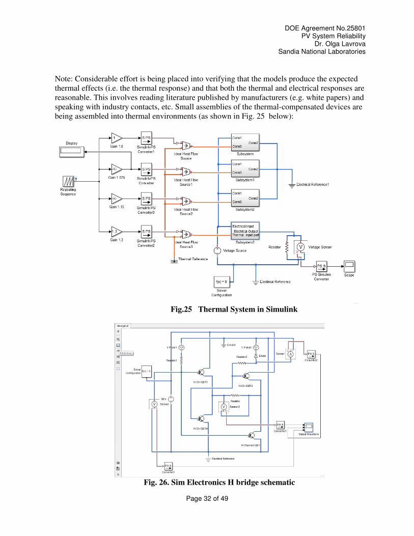
Task objectives: The broad programmatic problems have already been stated in FY14. In FY15 the inverter reliability research area will utilize the capabilities developed in FY14 to achieve the goal of a PLECS electro-thermal model that provides the design recommendations needed reduced inverter LCOE to DOE goals of $0.10/W. As previously noted for FY14, by investigating the reliability of proposed circuit topologies and optimizing the design of currently used circuit topologies and/or components, the inverter lifetime can be increased to reduced inverter LCOE to achieve DOE SunShot goals of $0.10/Wp. Achieving this goal will result in a minimum of 2.5x in cost reductions, consistent with DOE targets. For this investigation, Sandia will develop the Matlab Simulink/SymPowerSystems inverter electro-thermal performance model to predict the necessary changes to lower LCOE in a cost-effective manner under varying operating conditions and environments. Doing so will demonstrate an inverter design, derived from the Simulink/SymPowerSystems model, that can realistically achieve a 25-year lifetime under normal and advanced functionality usage conditions with manufacturing costs conducive to industry adoption.
Fig. 20. Overall layout of top-level Simulink model used for lifetime/ageing simulation of
inverter performance.
DOE Agreement No.25801 PV System Reliability
Dr. Olga Lavrova Sandia National Laboratories
Page 30 of 49
A significant amount of work concentrated on setting up device-level detailed description of existing Simulink models and planning for further detailed models.
• Device-level subsystems, which include both the thermal and electrical input functions, have been developed for the diode and n-channel MOSFET (see Fig. 20 and Fig.21 for an image of a diode and IGBT subsystem). A number of simulations have been run to determine an acceptable range of thermal parameters for a given device, with assumptions being made for heatsinking, electrical inputs, etc.
Fig.21 Diode Subsystem in Simulink
Fig.22 IGBT Subsystem in Simulink
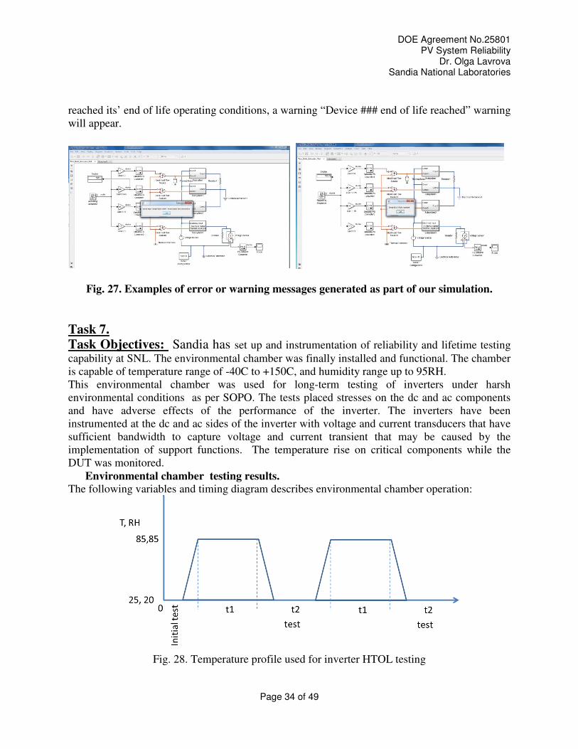
Based on the accuracy of these device models, additional subsystems will be developed including the IGBT and the capacitor. This work will continue in the next quarter of this project Some of the thermal parameters to be included are shown in Fig. 23.
DOE Agreement No.25801 PV System Reliability
Dr. Olga Lavrova Sandia National Laboratories
Page 31 of 49
Fig. 23. Thermal transfer parameters
• Thermal Mass, (in J/°K), Thermal Time Constant (s), and/or Thermal resistances have
been compiled (or approximately calculated) for several devices, based on datasheet values or estimated from device size, geometry, density, and specific heats. Sandia staff and a graduate intern in Mechanical engineering are being consulted on the methodology used in these calculations. Next steps will include using experimental data obtained in Task 9 of this project and using experimental values such as changes shown in Figure 24.
Fig. 24. Change in ICE after 1000 cycles at different temperatures obtained
experimentally at Sandia National Laboratories
DOE Agreement No.25801 PV System Reliability
Dr. Olga Lavrova Sandia National Laboratories
Page 32 of 49
Note: Considerable effort is being placed into verifying that the models produce the expected thermal effects (i.e. the thermal response) and that both the thermal and electrical responses are reasonable. This involves reading literature published by manufacturers (e.g. white papers) and speaking with industry contacts, etc. Small assemblies of the thermal-compensated devices are being assembled into thermal environments (as shown in Fig. 25 below):
Fig.25 Thermal System in Simulink
Fig. 26. Sim Electronics H bridge schematic
DOE Agreement No.25801 PV System Reliability
Dr. Olga Lavrova Sandia National Laboratories
Page 33 of 49
• Former grid-tied inverters have been disassembled (e.g. SMA 1800 W Sunny Boy) and the power electronic, capacitors, and heat-sinking elements have been catalogued and rendered as closely as possible in the models. Additional units across a variety of power ratings are available and will be examined as well.
• A rough method for device and ultimately, system-level stress (thermal, operational, and electrical) accumulation has been developed. The thermal history properties are expected to impact reliability, performance, and lifetime estimates. This is explained in more details in the following section.
Thermal Degradation Parameters:
To facilitate reliability, durability, and performance modeling, both the thermal history and age-related degradation should be modeled, and currently this capability needs to be added to the model (i.e. does not exist in SimElectronics). Typically the junction produces a great deal of heat, and depending on the operational mode (continuous or pulsed), different thermal response curves are used. We will focus on pulse-mode operation with heatsinks present and high, but variable, ambient temperatures, as this corresponds to the real-world conditions we are interested in understanding. Thermal parameters are characterized by the following table, where failures are estimated at 25% over common
Device Failure
Temp
(°C)
Failure
Temp-Secs
(°C-Secs)
Age Failure
(years) at
25 °C
Notes
Diode – Exponential 190 1.0E11 20
Capacitor –
Electrolytic
15 Unusual effect on lifetime for
electrolytics. Caps used for
filtering and as snubbers.
IGBT 190 7.5E10
20 Mortality assumed at 125% of
maximum junction temperature
MOSFETs 190 25 Mortality assumed at 125% of
maximum junction temperature
H-Bridge 180 25
Our model will keep track of cumulative operation parameters, at various temperatures, and will aggregate operation into Temp-Second or Temp-Minutes as appropriate. Based on particular wear-out or failure mechanisms of each component, a warning or an error message is generated, as shown in Figure 27 below. For example, if a device has been operating at a dangerously high temperature levels, a warning “ Device ## temperature too high” will appear. But, if a device
DOE Agreement No.25801 PV System Reliability
Dr. Olga Lavrova Sandia National Laboratories
Page 34 of 49
reached its’ end of life operating conditions, a warning “Device ### end of life reached” warning will appear.
Fig. 27. Examples of error or warning messages generated as part of our simulation.
Task 7.
Task Objectives: Sandia has set up and instrumentation of reliability and lifetime testing capability at SNL. The environmental chamber was finally installed and functional. The chamber is capable of temperature range of -40C to +150C, and humidity range up to 95RH. This environmental chamber was used for long-term testing of inverters under harsh environmental conditions as per SOPO. The tests placed stresses on the dc and ac components and have adverse effects of the performance of the inverter. The inverters have been instrumented at the dc and ac sides of the inverter with voltage and current transducers that have sufficient bandwidth to capture voltage and current transient that may be caused by the implementation of support functions. The temperature rise on critical components while the DUT was monitored.
Environmental chamber testing results.
The following variables and timing diagram describes environmental chamber operation:
Fig. 28. Temperature profile used for inverter HTOL testing
DOE Agreement No.25801 PV System Reliability
Dr. Olga Lavrova Sandia National Laboratories
Page 35 of 49
At the beginning of the test, DUTs was tested as per standard test, described in the table below. This will be used as t=0 test results. Following this, temp and humidity are to be ramped up (ramp up and down time depend on the chamber) and are to stay at these values for time t1 (200 hrs) After that time elapsed, the chamber is to be ramped down (ramp down time depending on the chamber) and DUT is to be tested again, as per procedure in the table below. The same pattern was to be repeated until the overall time at high temp, high humidity reached 1000hrs. This test is intended to resemble IED 61215 or 62093 test specs. All operating and characteristic values (such as component temperature) will be recorded during tests. Scheduled tests sequence for each testing interval:
Test num Test name Setting 1 Setting 2 Duration Other notes
1 Nominal P, PF
P=3000 W PF=1
5 min Powered up
2 P=1500 W 5 min
3
Nominal P, var PF P=3000
PF=0.9 5 min
4 PF=0.8 5 min
5 PF=-0.9 5 min
6 PF=-0.8 5 min
A typical performance profile is shown in Figure 29 below:
DOE Agreement No.25801 PV System Reliability
Dr. Olga Lavrova Sandia National Laboratories
Page 36 of 49
Fig. 29. Typical inverter performance under HTOL test
Task 9: Component Reliability
Task Objectives: Accurate component degradation profile lifetimes and failure modes are important to ensure adequate representation of long-term inverter operation in the electro-thermal model of Task 8. To account for secondary and tertiary inter-component effects during inverter operation, it is vital to understand isolated component degradation and failure mechanisms. Currently, manufacture-specific component-level reliability data does not necessarily include application-specific environments found in PV usage. In FY14, a single phase, single stage PV inverter test bed was developed. In FY15, analysis of this test bed under specific device degradation will be studied.
Component Degradation The first component to study was chosen to be the IGBT semiconductor switches, since their degradation directly affects the performance of the inverter. Infineon BSM50GB120DLC (1200 V, 100 A) full-bridge IGBT devices were chosen to test under long-term thermal cycling stress. Thermal cycling of IGBTs will affect the die
DOE Agreement No.25801 PV System Reliability
Dr. Olga Lavrova Sandia National Laboratories
Page 37 of 49
attachment to the copper board (DCB) due to CTE mismatch; causing void formation and fatigue-induced cracking from shear strain due to thermal cycles (Fig. 30). Voiding of the die attach layer will affect electrical control of the die, increasing parasitic resistance during the ON-state (and thus the power dissipated). CTE mismatch will also affect the attachment of bond wires to the die, resulting in an increase in VCE(on).
Figure 30: Packaging of a generic IGBT module. The module consists of a die and the elements used to control its electronic and thermal properties.
The IGBTs devices were electrically characterized using pulsed IV characterization and underwent thermal cycling stress in a thermal oven (room temperature to 150oC at 10oC/min ramp rate). This thermal stress was carried out for 500 cycles, when the devices were removed, re-characterized, and a sub-population returned to the thermal chamber for another 500 cycle stressing when they were again be removed, re-characterized, and a sub-population returned to the oven. This process continued until the entire population of IGBTs had varied degrees of degradation. Data presented here detailed the characterization of the IGBTs after 500 and 1000 cycles as compared to a pristine unit. After thermal cycling in the over, there is a clear change in current carrying capacity of the IGBT (Figure ). The change in ICE in the stressed devices compared to pristine due to thermal stress is small for VGE less than 5 V or greater than 11V. This is due to the fact that the absolute value of current is very low in the subthreshold region (VGE < 5V). In the large VGE region (VGE > 11 V), the shift is very small because the power supply used to measure the IGBTs goes into current compliance at 50 A, so the shift in current quickly goes to zero. However, in the threshold region of interest, there is clearly a change in the IV characteristics as the IGBT is stressed. The change in IV characteristics is more clearly seen in Figure 31 and 32, which shows the IV threshold curves of the IGBT population before (red line) and after (pink dots) thermal stress. The blue line indicates the shift in ICE value due to stressing. At 150oC in the region of threshold turn-on (VGE~ 6 V), the current through the stressed devices is lower than the pristine devices. However, at high current carrying gate voltages (VGE ~ 10 V), the cycled devices actually carry more current than the pristine devices.
DOE Agreement No.25801 PV System Reliability
Dr. Olga Lavrova Sandia National Laboratories
Page 38 of 49
Figure 31: Change in ICE vs VGE at different temperatures for IGBT units after 1000 cycles.
Figure 32: Change in threshold IV characteristics of an IGBT at 150oC before and after 1000 thermal cycles
This information can be summarized for all temperatures and devices in Fig. 33. The
maximum value of ∆ICE (immediately before power supply current compliance) is shows as a function of unit temperature for 500 (red dots) and 1000 (black dots) thermal cycles. After 500 thermal cycles, there is a slight change in ICE at temperatures less than 100oC. At 150oC, there is a decrease in ICE in the stressed units. This bipolar temperature dependence is frequently seen in MOSFET devices due to material quality effects in the conduction channel.
After 1000 cycles, the same bipolar effect is seen, although the baseline ∆ICE has shifted to greater values. The change in ICE from a pristine to a device after 1000 cycles can vary by 5-6 A.
Figure 33: Maximum change in current carrying of IGBTs (immediately before compliance limit) compared to pristine units after 500 (red dots) and 1000 (black dots) thermal cycles.
Through the work in this last quarter, it has been demonstrated that thermal cycling has altered the parameters of the IGBT current conduction significantly compared to pristine units. In the next quarter, the performance of pristine IGBTs as well as units which have been stressed at 500, 1000, and 1500 cycles will be compared in an to determine effect on inverter performance and power quality.
Inverter Reliability Workshop In FY15, Sandia has also been working in conjunction with Sarah Kurtz at NREL to host an inverter reliability workshop in parallel with NREL’s module-focused PVQAT workshop. This workshop took place on Wednesday, February 25th in Golden, CO and had focus areas ranging from component-level failure mechanisms to system-level testing (see agenda below). The workshop had 54 participants from a wide variety of industry stakeholders. There was vigorous discussion during all the sessions with many sessions going over time due to the amount of debate. Utility-Scale Inverters—Greg Ball (Chair), DNV GL
• “Inverter Reliability”—Matt Ursino, Solectria
• “Accelerated Reliability Testing of Commercial and Utility PV Inverters”—
Ron Vidano, Advanced Energy Module Level Power Electronics—Jack Flicker (Chair), Sandia National Laboratories
-2
0
2
4
6
8
0 50 100 150 200
∆∆ ∆∆I C
E(A
)
Temperature (oC)
1000 cycles
500 cycles
DOE Agreement No.25801 PV System Reliability
Dr. Olga Lavrova Sandia National Laboratories
Page 40 of 49
• “Standardization and Reliability Testing of Module-Level Power Electronics
(MLPE)”—Govindasamy Tamizhmani, TUV PTL
• “Determination of Mean Time to Failure” — Eric Boskin, Maxim Integrated
• “Managing Large Inverter Fleets”—Mark Baldassari, Enphase Energy Advanced Inverter Functionality—Faraz Ebneali (Chair), ReneSola
• “Smart Inverter Grid Support Functions and Potential Impact on
Reliability”—Aminul Huque, EPRI
• “The Impact of Smart Inverters: How Rule and Regulation Will Transform DG
into Smart Systems”—John Berdner, Enphase Energy Failure Modes—Chris Deline (Chair), NREL
• “IGBT Failure Modes in Inverters”—Diganta Das, CALCE
• “Corrosion of Electronics”—Rob Sorensen, Sandia National Laboratories
• “Nanocoatings: The Solution to All of Our Environmental Protection
Problems?”—Greg Caswell, DfR Solutions Accelerated Testing —Tim Peshek (Chair), Case Western Reserve University
• “PV Inverter Accelerated Testing for High-Humidity Environments”—Paul
Parker, SunPower
• “Reliability Testing of Inverters” Michael Mills-Price, DNV GL
• “Predictive Reliability Modeling for Inverters Based on Electro-Thermal
Phenomena”—Ken Armijo, Sandia National Laboratories All attendees were required to take part in a survey that details inverter performance, usage, and reliability across the industry. Survey results were compiled and published at the workshop. The survey results, as well as all the presentations are available for download at http://www.nrel.gov/pv/performance_reliability/pvmrw_20150225_wed_inverter.html
Component Losses for Inverter Advanced Functionality The large-scale penetration of variable and intermittent distributed resources into the electrical grid can have significant effects on frequency and voltage stability of the grid. It is predicted that as penetration ratios increase, the number and severity of grid parameter deviations from nominal will also increase (especially far away from distribution feeders). Historically, distributed generation has had such a low penetration ratio that, in low-voltage events, PV inverters have been asked to disconnect from the grid in order to prevent an islanding situation from occurring (since removing the active power of a small numbers of inverters on the grid was not sufficient to exacerbate the voltage deviation). However, as the penetration ratio increases and the power generated by distributed resources becomes non-negligible, PV inverters that disconnect from the grid can exacerbate the voltage deviations, decreasing grid reliability issues in the future. Therefore, new rules, such as the California Public Utility Commission’s (CPUC) Rule 21 interconnect requirements, are being implemented which demand that inverters ride-through a low (or high) voltage event. In Hawaii, where upwards of 12% of
DOE Agreement No.25801 PV System Reliability
Dr. Olga Lavrova Sandia National Laboratories
Page 41 of 49
households have rooftop solar, the ride through requirements had to be expanded due to the larger voltage fluctuations on the island grid (which has significantly less inertia than other grids). In the future, as the number of distributed resources on the grid increases, the frequency of voltage excursion may increase. Thus, the increased losses of a PV inverter during a ride-through event may become a non-negligible aspect to the unit reliability over its lifetime. In the new interconnection requirements, the voltage level of the ride through event determines the mode of operation of the inverter. For example, for Rule 21, in the event of a voltage sag lower than 0.5 PU (Vsag > 0.5 PU), the device under test must cease to energize and ride through the voltage sag for a duration of 1 second. If the voltage recovers above 0.5 PU within 1 second, then the inverter must resume energizing the utility up to 90% of pre-event power level within 1 second. An example of an inverter riding through in this manner is shown below (Fig. 35). During the ride through event, the ac current has a 36% transient spike and the dc voltage experiences a 24.3% voltage transient as the DC bus immediately returns to open circuit. During the low grid voltage condition, the inverter ceases to energize the utility. When the grid voltage returns to nominal, the dc voltage experiences a ringing transient voltage waveform. This ringing results in an increase in bus voltage above open circuit, to 500 V, which applies additional voltage stress to the DC-side components. After this transient, the inverter commences to return to its previous operating conditions and commences maximum power point tracking and power export.
A residential inverter with EPS support capability was evaluated in a laboratory setting to investigate possible stresses on the dc and ac components and any adverse effects of the performance of the inverter when the inverter goes through a grid voltage
Fig. 35: System voltages and current from a LVRT event
DOE Agreement No.25801 PV System Reliability
Dr. Olga Lavrova Sandia National Laboratories
Page 42 of 49
anomaly. The inverter analyzed has L/HVRT capabilities, but does not adhere to Rule 21 requirements due to the lack of a momentary cessation function. Voltage and current waveforms of MOSFET switches were recorded simultaneously along with system-level information in a 3 kW residential inverter during low voltage ride through events ranging from 0-1.5 s with Vsag ranging from 0-220 V. MOSFET voltage was monitored via Tektroniks voltage probes with drain-source current measured via a mini Rogowski coil. To minimize variations in the readings, DC power was provided by an Ametek PV simulator. Grid transients were simulated using a California instruments RS90 grid simulator. Tests were conducted at PV input powers of 3.29 kW provided by 14 Sanyo HIT 200 and 44 Astro-Power 75 simulated modules, respectively. Electrical data was collected via an Agilent DPO 3014 oscilloscope and analyzed with MATLAB.
Fig. 37: Normalized energy loss per switch for LVRT events (Vsag=43 V) of different durations from 0-1.5 s. The energy loss per switch is independent of ride-through time, indicating that the inverter is actively exporting energy for all LVRT events.
Fig. 36.: Normalized energy loss per switch for LVRT events of different Vsag values from 0-240 V with durations of 1-1.5 s (in the “cease to energize” regime for Vsag=0-120 V).
DOE Agreement No.25801 PV System Reliability
Dr. Olga Lavrova Sandia National Laboratories
Page 43 of 49
Cumulative MOSFET switching loss during each voltage transient event was calculated and then normalized by the duration of the event in order to determine the relative severity of the LVRT event. The results of normalized energy loss per switch as a function of ride through time and Vsag are shown in Fig. 36 and Fig. 37, respectively. As can be seen from Fig. 36, the rate of energy loss during the event is independent of event length with a value of approximately 682±40 J/s. This indicates that for all LVRT events the inverter attempts to export energy. Since the inverter in question does not adhere to Rule 21, it never enters the “cease to energize” state (0-0.5 PU for tevent < 1 s, shown by the dashed blue line) nor does it disconnect when the ride through event is longer than 1 s. Such behavior would be evident from Fig. 36. Since, at 0.195 PU, the corresponding Rule 21 behaviors are “momentary cessation” and “disconnect”, the normalized energy loss of a Rule 21 compliant inverter would be close to zero. For the residential inverter studied, the rate of energy loss during an LVRT event is linearly related to the value of Vsag (Fig. 37) with a maximum normalized energy loss equal to 879 J/s for Vsag = 0V. The energy loss decreases at a rate of approximately -3.5 J/V as Vsag increases until the energy loss is zero at a PU of unity. Each of the ride through events represented in Fig. has a duration greater than 1 s. This means that to be Rule 21 compliant, the inverter should cease to export power and for all Vsag< 0.5 PU (120 V), shown as the solid blue line. So a Rule 21 inverter should have a linear increase in normalized energy loss until 0.5 PU. For Vsag < 0.5 PU, the normalized energy loss should be nearly zero due to the “momentary cessation” operation mode. Based on the data presented here, it is apparent that an inverter that rides through a low voltage event experiences increased losses compared to normal operation. The new CPUC Rule 21 interconnection requirements, especially the “momentary cessation” operation mode, will tend to decrease the LVRT losses of inverters for voltage transients below 0.5 PU. References:
[1] H. Laukamp, "Statistical Failure Analysis of German PV Installations," in PV Brandsicherheit Workshop, Köln, Germany, 26 Jan. 2012 (in German).
[2] K. M. Armijo, J. Johnson, M. Hibbs, and A. Fresquez, "Characterizing Fire Danger from Low Power PV Arc-Faults," presented at the 40th IEEE PVSC, Denver, CO, 2014.
[3] L. Schirone, F. P. Califano, U. Moschella, and U. Rocca, "Fault finding in a 1 MW photovoltaic plant by reflectometry," presented at the 24th IEEE Photovoltaic Specialists Conference, 1994.
[4] T. Takashima, J. Yamaguchi, and M. Ishida, "Fault detection by signal response in PV module strings," presented at the 33rd Photovoltaic Specialists Conference (PVSC), San Diego, CA, 2008.
[5] T. Takashima, J. Yamaguchi, K. Otani, K. Kato, and M. Ishida, "Experimental Studies of Failure Detection Methods in PV Module Strings," presented at the 2006 IEEE Photovoltaic Energy Conversion, 2006.
[6] T. Takashima, J. Yamaguchi, K. Otani, T. Oozeki, K. Kato, and M. Ishida, "Experimental studies of fault location in PV module strings," Solar Energy Materials & Solar Cells pp. 1079–1082, 2009.
DOE Agreement No.25801 PV System Reliability
Dr. Olga Lavrova Sandia National Laboratories
Page 44 of 49
[7] C. Furse, Y. C. Chung, C. Lo, and P. Pendayala, "A Critical Comparison of Reflectometry Methods for Location of Wiring Faults," Smart Structures and Systems, vol. 2, pp. 25-46, 2006.
[8] J. Flicker and J. Johnson, "Analysis of Fuses for "Blind Spot" Ground Fault Detection in Photovoltaic Systems," Solar American Board for Codes and Standards July 2013.
[9] G. Ball, B. Brooks, J. Johnson, J. Flicker, A. Rosenthal, J. Wiles, et al., "Inverter ground-fault detection ‘blind spot’ and mitigation methods," Solar American Board for Codes and Standards 2013.
[10] M. K. Alam, F. Khan, J. Johnson, and J. Flicker, "PV ground-fault detection using spread spectrum time domain reflectometry (SSTDR)," in Energy Conversion Congress and Exposition (ECCE), 2013 IEEE, 2013, pp. 1015-102.
[11] "$1/Watt Photovoltaic Systems," US Department of Energy, White Paper2010. [12] Y. Xue, K. C. Divya, G. Griepentrog, M. Liviu, S. Suresh, and M. Manjrekar, "Towards
Next Generation Photovoltaic Inverters," presented at the 2011 IEEE Energy Conversion Congress and Exposition (ECCE), 2011.
[13] L. Bony, S. Doig, C. Hart, and E. Maurer, Achieving low-cost solar PV: Industry Workshop Recommendations for Near-term Balance of System Cost Reductions: Rocky Mountain Institute (RMI), 2010.
[14] B. Jablonska, H. Kaan, M. Leeuwen, and G. Boer, "PV-prive Project at ECN: Five Years of Experience With Small-scale AC Module PV Systems," Presented at the 20th European Photovoltaic Solar Energy Coference and Exhibition, 2005.
[15] A. Ristow, M. Begovic, A. Pregelj, and A. Rohatgi, "Development of a Methodology for Improving Photovoltaic Inverter Reliability," IEEE Transactions on Industrial Electronics, vol. 55, pp. 2581-2592, Jul 01 2008.
[16] A. Maish, "Defining Requirements for Improved Photovoltaic System Reliability," Progress in Photovoltaics, pp. 165-173, 1999.
[17] A. B. Maish, C. Atcitty, S. Hester, D. Greenberg, D. Osborn, D. Collier, et al., "Photovoltaic System Reliability," presented at the Conference Record of the Twenty Sixth IEEE Photovoltaic Specialists Conference, 1997, 1997.
[18] A. Golnas, "PV System Reliability: An Operator's Perspective," IEEE Journal of Photovoltaics, pp. 1-6.
[19] IEEE, "1547-IEEE Standard for Interconnecting Distributed Resources With Electric Power Systems," IEEE2003.
[20] I. E. C. 61727, "IEC61727-Photovoltaic (PV) systems: Characteristics of the Utility Interface," International Electrotechnical Commission1996.
[21] D. Xiang, L. Ran, P. Tavner, S. Yang, A. Bryant, and P. Mawby, "Condition Monitoring Power Module Solder Fatigue Using Inverter Harmonic Identification," Power Electronics, IEEE Transactions on, vol. 26, pp. 235-247, Dec 01 2011.
[22] J. R. Celaya, A. Saxena, C. S. Kulkarni, S. Saha, and K. Goebel, "Prognostics approach for power MOSFET under thermal-stress aging," presented at the Reliability and Maintainability Symposium (RAMS), 2012 Proceedings - Annual, 2012.
[23] G. Sonnenfeld, K. Goebel, and J. R. Celaya, "An agile accelerated aging, characterization and scenario simulation system for gate controlled power transistors," IEEE Autotestcon. Proceedings, pp. 208-215, Sep 08 2008.
DOE Agreement No.25801 PV System Reliability
Dr. Olga Lavrova Sandia National Laboratories
Page 45 of 49
[24] E. Hofreiter and A. M. Bazzi, "Single-stage boost inverter reliability in solar photovoltaic applications," presented at the Power and Energy Conference at Illinois (PECI), 2012 IEEE, 2012.
[25] B. Gu, J. Dominic, J.-S. Lai, C.-L. Chen, T. LaBella, and B. Chen, "High Reliability and Efficiency Single-Phase Transformerless Inverter for Grid-Connected Photovoltaic Systems," Power Electronics, IEEE Transactions on, vol. 28, pp. 2235-2245, Jun 2013.
[26] J. Lehmann, M. Netzel, R. Herzer, and S. Pawel, "Method for electrical detection of bond wire lift-off for power semiconductors," Audio, Transactions of the IRE Professional Group on, pp. 333-336, May 14 2003.
[27] R. Morgolis, "A Review of PV Inverter Technology Cost and Performance Projections," National Renewable Energy Laboratory2006.
[28] IEC Standard 61215, "Crystalline silicon terrestrial photovoltaic (PV) modules. Design qualification and type approval," ed. 2.0: Geneva, 2005.
[29] H. Huang, A. T. Bryant, and P. A. Mawby, "Electro-thermal Modeling of Three Phase Inverters," in 14th European Conference on Power Electronics and Applications, 2011.
[30] T. Kojima, Y. Yamada, M. Ciappa, M. Chiavarini, and W. Fichtner, "A Novel electro-thermal Simulation Approach of Power IGBT Modules for Automotive Traction Applications," in 2004 IEEE International Conference on Solid Dielectrics, 2004 (ICSD 2004), Kitakyushu, 2004.
[31] H. Schmidt and F. Reil, "Welcome to the 2nd Workshop ‘PV Fire’," presented at the PV Brandsicherheit Workshop, Freiburg, Jan 2013 (in German).
[32] H. Laukamp and H. Schmidt, "Zusammenfassung Schadensfallerhebung und analyse," presented at the PV Brandsicherheit Workshop, Cologne, April 2014 (in German).
[33] J. Johnson and K. Armijo, "Parametric Study of PV Arc-Fault Generation Methods and Analysis of Conducted DC Spectrum," presented at the 40th IEEE PVSC, Denver, CO, 2014.
[34] J. Flicker and J. Johnson, "Recommendations for RCD Ground Fault Detector Trip Thresholds," presented at the EU PVSEC, Amsterdam, Netherlands, 2014.
[35] J. Flicker, J. Johnson, M. Albers, and G. Ball, "Recommendations for CSM and Riso Ground Fault Detector Trip Thresholds," presented at the 40th IEEE PVSC, Denver, CO, 2014.
[36] U. Laboratories, "1741 Certification Requirement Decision," in Non-Isolated EPS Interactive PV Inverters Rated Less Than 30Kva, ed, 2010.
[37] U. Laboratories, "1741 Certification Requirement Decision," in Isolated Inverters Intended for Use with Ungrounded PV Arrays, ed, 2012.
[38] K. M. Armijo, J. Johnson, R. K. Harrison, K. E. Thomas, M. Hibbs, and A. Fresquez, "Quantifying Photovoltaic Fire Danger Reduction with Arc-Fault Circuit Interrupters," Progress in Photovoltaics, in review 2014.
[39] W. Gardiner, "Work Instruction for Arc Fault RetrofiT," Power One Product Engineering2014.
[40] H. Haeberlin, "Overview of Long-Term Tests of Arc Fault Detectors (AFD) at the PV Laboratory of BUAS," in PV Brandsicherheit Meeting, Berlin, 2013.
[41] S. McConnell, Z. Wang, R. S. Balog, and J. Johnson, "Evaluation Method for Arc Fault Detection Algorithms," presented at the 40th IEEE PVSC, Denver, CO, 2014.
DOE Agreement No.25801 PV System Reliability
Dr. Olga Lavrova Sandia National Laboratories
Page 46 of 49
[42] [42] Z. Wang, S. McConnell, R.S. Balog, and J. Johnson, "Arc Fault Signal Detection - Fourier Transformation vs. Wavelet Decomposition Techniques using Synthesized Data," presented at the 40th IEEE PVSC, Denver, CO, 2014.
[43] Northern Arizona Wind & Sun and Advanced Solar Electric Technical Forum. (2014, 5 Aug, 2014). Arc fault on inverter. Available: http://forum.solar-electric.com/showthread.php?23106-arc-fault-on-inverter/
[44] M. K. Alam, F. H. Khan, J. Johnson, and J. Flicker, "PV arc-fault detection using spread spectrum time domain reflectometry (SSTDR) " presented at the IEEE Energy Conversion Congress and Exposition (ECCE), Pittsburgh, PA, 2014.
[45] M. Alam, F. H. Khan, J. Johnson, and J. Flicker, "A Comprehensive Review of Catastrophic Faults in PV Arrays: Types, Detection and Mitigation Techniques," IEEE Journal of Photovoltaics, in review 2014 2014.
[46] N. Gokmen, E. Karatepe, B. Celik, and S. Silvestre, "Simple diagnostic approach for determining of faulted PV modules in string based PV arrays," Solar Energy, vol. 86, pp. 3364–3377, November 2012 2012.
[49] Bender. (2014, 5 Aug, 2014). EDS3090 Series Portable Ground Fault Location System for Ungrounded (Floating) AC/DC Systems Available: http://www.bender.org/documents/EDS3090_datasheet_NAE1012031.pdf
[51] G. D. Hasenfus, "Smart sensors for solar panels," USA Patent US 2009/0140719 A1, 2009. [52] G. E. Presher Jr. and C. J. Warren, "System and method for monitoring photovoltaic power
generation systems," USA Patent US 8204709 B2, 2012. [53] J. Flicker and J. Johnson, "Electrical simulations of series and parallel PV arc-faults,"
presented at the IEEE 39th Photovoltaic Specialists Conference (PVSC), 2013, Tampa, FL, 2013.
[54] J. D. Flicker and J. Johnson, "Photovoltaic ground fault and blind spot electrical simulations," SAND2013-3459 ed. Albuquerque, NM: Sandia National Laboratories Technical Report SAND2013-3459, 2013.
[55] International Electrotechnical Commission (IEC) Standard 62109-2, "Safety of power converters for use in photovoltaic power systems - Part 2: Particular requirements for inverters ", ed. 1.0: Geneva, 2011.
[56] P. Hacke, K. Terwilliger, R. Smith, S. Glick, J. Pankow, M. Kempe, et al., "System voltage potential-induced degradation mechanisms in PV modules and methods for test," presented at the 37th IEEE PVSC, 2011.
[57] S. Hoffmann and M. Koehl, "Effect of humidity and temperature on the potential-induced degradation," Progress in Photovoltaics: Research and Applications, vol. 22, pp. 173–179, 2014.
[58] T. Bruckner and S. Bernet, "Estimation and measurement of junction temperatures in a three-level voltage source converter," IEEE Transactions on Power Electronics, vol. 22, pp. 3-12, 2007.
DOE Agreement No.25801 PV System Reliability
Dr. Olga Lavrova Sandia National Laboratories
Page 47 of 49
[59] D. Xu, et al., "Power loss and junction temperature analysis of power semiconductor devices," IEEE Transactions on Industry Applications, vol. 38, pp. 1426-1431, 2002.
[60] J. Johnson, B. Pahl, C. Luebke, T. Pier, T. Miller, J. Strauch, et al., "Photovoltaic DC Arc Fault Detector testing at Sandia National Laboratories," presented at the Photovoltaic Specialists Conference (PVSC), 2011 37th IEEE.
[61] Y. Chu, S. Wang, and R. Crosier, "Grid active power filters using cascaded multilevel inverters with direct asymmetric switching angle control for grid support functions," presented at the 28th IEEE Applied Power Electronics Conference and Exposition (APEC), 2013.
[62] S. Saridakis, E. Koutroulis, and F. Blaabjerg, "Optimal Design of Modern Transformerless PV Inverter Topologies," IEEE Transactions on Energy Conversion, vol. 28, pp. 394-404, Jul 2013.
[63] M. Victor, F. Greizer, S. Bremicker, and U. Hubler, "Method of converting a direct current voltage from a source of direct current voltage, more specifically from a photovoltaic source of direct current voltage, into a alternating current voltage," United States Patent US 7411802 B2, 2008.
[64] B. B. Yang, J. Johnson, K. M. Armijo, J. M. Taylor, and N. R. Sorensen, "Arc Fault Risk Assessment and Degradation Model Development for Photovoltaic Connectors," presented at the 40th IEEE PVSC, Denver, CO, 2014.
[65] National Electrical Code, 2011 Edition, NFPA70, National Fire Protection Association, Quincy, MA.
[66] Underwriters Laboratories 1699B, “Outline of Investigation for Photovoltaic (PV) DC Arc-Fault Circuit Protection, Issue 2, 14 Jan 2013.
[68] Priolo, M.A., Gamboa, D., K.M. Holder, and J.C. Grunlan, “Super gas barrier of transparent polymer – Clay multilayer ultrathin films,” Nano Lett., 10, pp. 4970-4974, 2010
[69] K.M. Armijo, J. Johnson, M. Hibbs, A. Fresquez, “Characterizing Fire Danger from Low Power PV Arc-Faults,” 40th IEEE PVSC, Denver, CO, 8-13 June, 2014.
[70] B. J. Baliga, Power semiconductor devices. Boston, MA: PWS Publishing Company, 1996. [71] D. W. Brown, M. Abbas, A. Ginart, I. N. Ali, P. W. Kalgren, and G. J. Vachtsevanos,
"Turn-Off Time as an Early Indicator of Insulated Gate Bipolar Transistor Latch-up," IEEE Transactions on Power Electronics, vol. 27 (2), pp. 479-489, 2012.
[72] H. Delambilly and H. Keser, "Failure Analysis of Power Modules - a Look at the Packaging and Reliability of Large IGBTs," IEEE Transactions on Components Hybrids and Manufacturing Technology, 1993.
[73] W. Wu, M. Held, P. Jacob, P. Scacco, and A. Birolini, "Proceedings of International Symposium on Power Semiconductor Devices and IC's: ISPSD '95," International Symposium on Power Semiconductor Devices and IC's: ISPSD '95, 1995.
[74] V. A. Sankaran, C. Chen, C. S. Avant, and X. Xu, "Power Cycling Reliability of IGBT Power Modules," IEEE Industry Applications Society Annual Meeting (IAS), 1997.
DOE Agreement No.25801 PV System Reliability
Dr. Olga Lavrova Sandia National Laboratories
Page 48 of 49
[75] J. Flicker, R. Kaplar, B. Yang, M. Marinella, and J. Granata, "Insulated gate bipolar transistor reliability testing protocol for PV inverter applications," Progress in Photovoltaics: Research and Applications, vol. 22 (9), pp. 970-983, Sep 01 2014.
[76] Lavrova, Olga A., and Daniel J. Blumenthal. "Accelerated aging studies of multi-section tunable GCSR lasers for dense WDM applications." Lightwave Technology, Journal of 18, no. 12 (2000): 2196-2199.
[77] Osinsky, A., Y. Qiu, J. Mahan, H. Temkin, S. A. Gurevich, S. I. Nesterov, E. M. Tanklevskaia, V. Tretyakov, O. A. Lavrova, and V. I. Skopina. "Novel wet chemical etch for nanostructures based on II-VI compounds." Applied physics letters 71, no. 4 (1997): 509-511.
[78] Gurevich, S. A., O. A. Lavrova, N. V. Lomasov, S. I. Nesterov, V. I. Skopina, E. M. Tanklevskaya, V. V. Travnikov et al. "ZnCdSe/ZnSe quantum well wires fabricated by reactive ion etching and wet chemical treatment." Semiconductor science and technology 13, no. 1 (1998): 139.
[79] Li, Nein-Yi, Doug Collins, Shashank Jatar, Olga Lavrova, Chris Helms, Wenlin Luo, Linlin Liu et al. "Design and manufacturing of 10G GenX VCSELs at Emcore." In Integrated Optoelectronic Devices 2007, pp. 648402-648402. International Society for Optics and Photonics, 2007.
[80] Li, D., Jayaweera, S. K., Lavrova, O., & Jordan, R. (2011, April). “Load management for price-based demand response scheduling-a block scheduling model”. In International Conference on Renewable Energies and Power Quality (ICREPQ’11),(Las Palmas de Gran Canaria, Spain).
[81] Takumi Takashima, Junji Yamaguchi, Kenji Otani, Takashi Oozeki, Kazuhiko Kato, MasayoshiIshida, “Experimental studies of fault location in PV module strings”, Solar Energy Materials & Solar Cells (2009),1079–1082.
[82] Takashima, T.; Yamaguchi, Junji; Ishida, Masayoshi, "Fault detection by signal response in PV module strings," Photovoltaic Specialists Conference, 2008. PVSC '08. 33rd IEEE, vol., no., pp.1, 5, 11-16 May 2008.
[83] Takashima, T.; Yamaguchi, Junji; Otani, K.; Kato, K.; Ishida, M., "Experimental Studies of Failure Detection Methods in PV Module Strings," Photovoltaic Energy Conversion, Conference Record of the 2006 IEEE 4th World Conference on, vol.2, no., pp.2227-2230, 7-12 May 2006.
[84] Schirone, L.; Califano, F. P.; Moschella, U.; Rocca, U., "Fault finding in a 1 MW photovoltaic plant by reflectometry," Photovoltaic Energy Conversion, 1994., Conference Record of the Twenty Fourth. IEEE Photovoltaic Specialists Conference - 1994, 1994 IEEE First World Conference on , vol.1, no., pp.846,849 vol.1, 5-9 Dec 1994.
[85] C. Furse, Y. C. Chung, C. Lo, P. Pendayala, “A Critical Comparison of Reflectometry Methods for Location of Wiring Faults,” Smart Structures and Systems, vol 2, Issue 1, pp. 25-46, 2006.
[86] M. K. Alam, F. H. Khan, J. Johnson, and J. Flicker, “PV ground-fault detection using spread spectrum time domain reflectometry (SSTDR)”, IEEE Energy Conversion Congress and Expo (ECCE), Denver, 15-19 Sept., 2013.
[87] M. K. Alam, F. H. Khan, J. Johnson, and J. Flicker, “PV faults: overview, modeling, prevention and detection techniques”, IEEE Control and Modeling for Power Electronics (COMPEL), Salt Lake City, UT, 23-26 June, 2013.
DOE Agreement No.25801 PV System Reliability
Dr. Olga Lavrova Sandia National Laboratories
Page 49 of 49
[88] J. Flicker and J. Johnson, “Photovoltaic ground fault and blind spot electrical simulations,” Sandia National Laboratories Technical Report, SAND2013-3459, June 2013.
[89] J. Flicker and J. Johnson, “Analysis of fuses for ‘blind spot’ ground fault detection in photovoltaic power systems,” Solar America Board for Codes and Standards Report, June 2013.
[90] G. Ball, B. Brooks, J. Johnson, J. Flicker, A. Rosenthal, J. Wiles, L. Sherwood, M. Albers, and T. Zgonena, “Inverter ground-fault detection ‘blind spot’ and mitigation methods,” Solar America Board for Codes and Standards Report, June 2013.
[91] Brooks, B. (January 2012). The ground-fault protection blind spot: Safety concern for larger PV systems, U.S. Solar American Board for Codes and Standards Report. www.solarabcs.org/about/publications/reports/blindspot/.
[92] H. Huang, A. T. Bryant, and P. A. Mawby, "Electro-thermal Modeling of Three Phase Inverters," 14th European Conference on Power Electronics and Applications, 2011, 2011.
[93] T. Kojima, Y. Yamada, M. Ciappa, M. Chiavarini, and W. Fichtner, "A Novel electro-thermal Simulation Approach of Power IGBT Modules for Automotive Traction Applications," Proceedings of the 2004 IEEE International Conference on Solid Dielectrics, 2004 (ICSD 2004), Kitakyushu, 2004.
A. R. Hefner, "A dynamic electro-thermal model for the IGBT," IEEE Transactions on Industry Applications, vol. 30 (2), pp. 394-405, 1994.
[94] A.Ristowand and M. Begovic, “Development of a methodology for improving photovoltaic inverter reliability,” IEEE Trans. Ind. Electron., vol. 55, no. 7, pp. 2591-2592, Jul. 2008.