2002 Microchip Technology Inc. DS21444C-page 1 M TC642 Features • Temperature Proportional Fan Speed for Acoustic Control and Longer Fan Life • Efficient PWM Fan Drive • 3.0V to 5.5V Supply Range: - Fan Voltage Independent of TC642 Supply Voltage - Supports any Fan Voltage • FanSense™ Fault Detection Circuits Protect Against Fan Failure and Aid System Testing • Shutdown Mode for "Green" Systems • Supports Low Cost NTC/PTC Thermistors • Space Saving 8-Pin MSOP Package • Over-temperature Indication Applications • Power Supplies • Personal Computers • File Servers • Telecom Equipment • UPSs, Power Amps, etc. • General Purpose Fan Speed Control Available Tools • Fan Controller Demonstration Board (TC642DEMO) • Fan Controller Evaluation Kit (TC642EV) Package Types General Description The TC642 is a switch mode fan speed controller for use with brushless DC fans. Temperature proportional speed control is accomplished using pulse width mod- ulation (PWM). A thermistor (or other voltage output temperature sensor) connected to the V IN input fur- nishes the required control voltage of 1.25V to 2.65V (typical) for 0% to 100% PWM duty cycle. Minimum fan speed is set by a simple resistor divider on the V MIN input. An integrated Start-up Timer ensures reliable motor start-up at turn-on, coming out of shutdown mode or following a transient fault. A logic low applied to V MIN (Pin 3) causes fan shutdown. The TC642 also features Microchip Technology's pro- prietary FanSense™ technology for increasing system reliability. In normal fan operation, a pulse train is present at SENSE (Pin 5). A missing pulse detector monitors this pin during fan operation. A stalled, open or unconnected fan causes the TC642 to trigger its Start-up Timer once. If the fault persists, the FAULT output goes low and the device is latched in its shut- down mode. FAULT is also asserted if the PWM reaches 100% duty cycle, indicating a possible thermal runaway situation, although the fan continues to run. See Section 5.0, “Typical Applications”, for more information and system design guidelines. The TC642 is available in the standard 8-pin plastic DIP, SOIC and MSOP packages and is available in the commercial, extended commercial and industrial temperature ranges. 1 8 2 7 3 6 4 5 TC642 GND C F V IN V MIN FAULT SENSE V DD V OUT SOIC/PDIP/MSOP PWM Fan Speed Controller with FanSense ™ Technology
Transcript
M TC642PWM Fan Speed Controller with FanSense™ Technology
Features• Temperature Proportional Fan Speed for Acoustic
Control and Longer Fan Life• Efficient PWM Fan Drive• 3.0V to 5.5V Supply Range:
- Fan Voltage Independent of TC642 Supply Voltage
- Supports any Fan Voltage• FanSense™ Fault Detection Circuits Protect
Against Fan Failure and Aid System Testing• Shutdown Mode for "Green" Systems• Supports Low Cost NTC/PTC Thermistors• Space Saving 8-Pin MSOP Package• Over-temperature Indication
Applications• Power Supplies• Personal Computers• File Servers• Telecom Equipment• UPSs, Power Amps, etc.• General Purpose Fan Speed Control
Available Tools• Fan Controller Demonstration Board (TC642DEMO)• Fan Controller Evaluation Kit (TC642EV)
Package Types
General DescriptionThe TC642 is a switch mode fan speed controller foruse with brushless DC fans. Temperature proportionalspeed control is accomplished using pulse width mod-ulation (PWM). A thermistor (or other voltage outputtemperature sensor) connected to the VIN input fur-nishes the required control voltage of 1.25V to 2.65V(typical) for 0% to 100% PWM duty cycle. Minimum fanspeed is set by a simple resistor divider on the VMINinput. An integrated Start-up Timer ensures reliablemotor start-up at turn-on, coming out of shutdownmode or following a transient fault. A logic low appliedto VMIN (Pin 3) causes fan shutdown.
The TC642 also features Microchip Technology's pro-prietary FanSense™ technology for increasing systemreliability. In normal fan operation, a pulse train ispresent at SENSE (Pin 5). A missing pulse detectormonitors this pin during fan operation. A stalled, openor unconnected fan causes the TC642 to trigger itsStart-up Timer once. If the fault persists, the FAULToutput goes low and the device is latched in its shut-down mode. FAULT is also asserted if the PWMreaches 100% duty cycle, indicating a possible thermalrunaway situation, although the fan continues to run.See Section 5.0, “Typical Applications”, for moreinformation and system design guidelines. The TC642 is available in the standard 8-pin plasticDIP, SOIC and MSOP packages and is available in thecommercial, extended commercial and industrialtemperature ranges.
1 8
2 7
3 6
4 5
TC642
GND
CF
VIN
VMIN FAULT
SENSE
VDD
VOUT
SOIC/PDIP/MSOP
2002 Microchip Technology Inc. DS21444C-page 1
TC642
Functional Block Diagram
FAULT
SHDN
SENSE
OTF
GND
70mV (typ.)
10kΩ
VMIN
VIN
CF
VDD
VOUT
TC642
ControlLogic
+
–VOTF
VSHDN
+
–
–
+
+
–
+
–
3 x TPWMTimer
Start-upTimer
ClockGenerator
MissingPulseDetect
DS21444C-page 2 2002 Microchip Technology Inc.
TC642
1.0 ELECTRICAL
CHARACTERISTICSAbsolute Maximum Ratings*Supply Voltage ......................................................... 6V
Input Voltage, Any Pin.... (GND – 0.3V) to (VDD +0.3V)Package Thermal Resistance:
Specified Temperature Range ........... -40°C to +125°C
Storage Temperature Range.............. -65°C to +150°C
*Stresses above those listed under "Absolute Maximum Rat-ings" may cause permanent damage to the device. These arestress ratings only and functional operation of the device atthese or any other conditions above those indicated in theoperation sections of the specifications is not implied. Expo-sure to absolute maximum rating conditions for extended peri-ods may affect device reliability.
ELECTRICAL SPECIFICATIONS
Note 1: Ensured by Design, not tested.
Electrical Characteristics: TMIN < TA < TMAX, VDD = 3.0V to 5.5V, unless otherwise specified.
Symbol Parameter Min Typ Max Units Test Conditions
VDD Supply Voltage 3.0 — 5.5 VIDD Supply Current, Operating — 0.5 1.0 mA Pins 6, 7 Open,
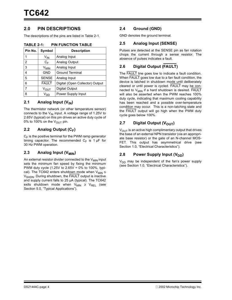
2.0 PIN DESCRIPTIONSThe descriptions of the pins are listed in Table 2-1.
TABLE 2-1: PIN FUNCTION TABLE
2.1 Analog Input (VIN)The thermistor network (or other temperature sensor)connects to the VIN input. A voltage range of 1.25V to2.65V (typical) on this pin drives an active duty cycle of0% to 100% on the VOUT pin.
2.2 Analog Output (CF)CF is the positive terminal for the PWM ramp generatortiming capacitor. The recommended CF is 1 µF for30 Hz PWM operation.
2.3 Analog Input (VMIN)An external resistor divider connected to the VMIN inputsets the minimum fan speed by fixing the minimumPWM duty cycle (1.25V to 2.65V = 0% to 100%, typi-cal). The TC642 enters shutdown mode when VMIN ≤VSHDN. During shutdown, the FAULT output is inactiveand supply current falls to 25 µA (typical). The TC642exits shutdown mode when VMIN ≥ VREL (seeSection 5.0, “Typical Applications”).
2.4 Ground (GND)GND denotes the ground terminal.
2.5 Analog Input (SENSE)Pulses are detected at the SENSE pin as fan rotationchops the current through a sense resistor. Theabsence of pulses indicates a fault.
2.6 Digital Output (FAULT)The FAULT line goes low to indicate a fault condition.When FAULT goes low due to a fan fault condition, thedevice is latched in shutdown mode until deliberatelycleared or until power is cycled. FAULT may be con-nected to VMIN if a hard shutdown is desired. FAULTwill also be asserted when the PWM reaches 100%duty cycle, indicating that maximum cooling capabilityhas been reached and a possible over-temperaturecondition may occur. This is a non-latching state andthe FAULT output will go high when the PWM dutycycle goes below 100%.
2.7 Digital Output (VOUT)VOUT is an active high complimentary output that drivesthe base of an external NPN transistor (via an appropri-ate base resistor) or the gate of an N-channel MOS-FET. This output has asymmetrical drive (seeSection 1.0, “Electrical Characteristics”).
2.8 Power Supply Input (VDD)VDD may be independent of the fan’s power supply(see Section 1.0, “Electrical Characteristics”).
Pin No. Symbol Description
1 VIN Analog Input2 CF Analog Output3 VMIN Analog Input4 GND Ground Terminal5 SENSE Analog Input6 FAULT Digital (Open Collector) Output7 VOUT Digital Output8 VDD Power Supply Input
DS21444C-page 4 2002 Microchip Technology Inc.
TC642
3.0 DETAILED DESCRIPTION
3.1 PWMThe PWM circuit consists of a ramp generator andthreshold detector. The frequency of the PWM is deter-mined by the value of the capacitor connected to the CFinput. A frequency of 30 Hz is recommended(CF = 1 µF). The PWM is also the time base for theStart-up Timer (see Section 3.4, “Start-Up Timer”). ThePWM voltage control range is 1.25V to 2.65V (typical)for 0% to 100% output duty cycle.
3.2 FAULT OutputThe TC642 detects faults in two ways.
First, pulses appearing at SENSE due to the PWMturning on are blanked, with the remaining pulsesfiltered by a missing pulse detector. If consecutivepulses are not detected for 32 PWM cycles (≅ 1 Sec ifCF = 1 µF), the Diagnostic Timer is activated, and VOUTis driven high continuously for three PWM cycles(≅ 100 msec if CF = 1 µF). If a pulse is not detectedwithin this window, the Start-up Timer is triggered (seeSection 3.4). This should clear a transient fault condi-tion. If the missing pulse detector times out again, thePWM is stopped and FAULT goes low. When FAULT isactivated due to this condition, the device is latched inshutdown mode and will remain off indefinitely.
The TC642 may be configured to continuously attemptfan restarts, if so desired.
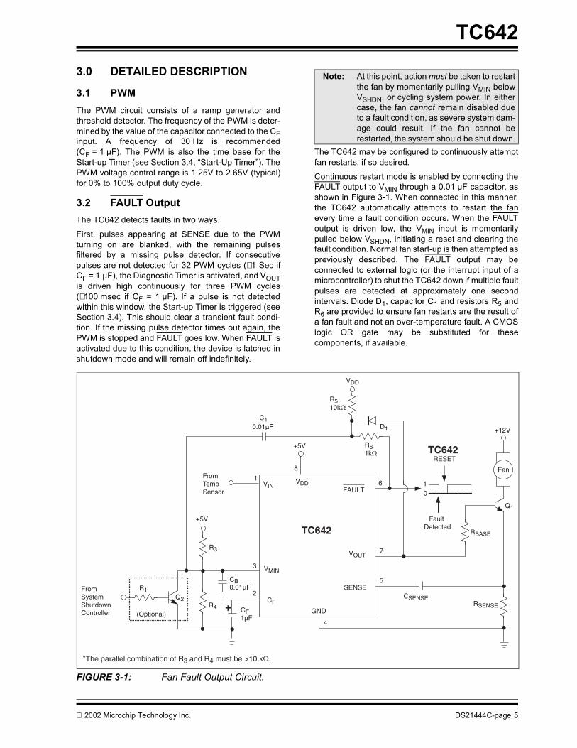
Continuous restart mode is enabled by connecting theFAULT output to VMIN through a 0.01 µF capacitor, asshown in Figure 3-1. When connected in this manner,the TC642 automatically attempts to restart the fanevery time a fault condition occurs. When the FAULToutput is driven low, the VMIN input is momentarilypulled below VSHDN, initiating a reset and clearing thefault condition. Normal fan start-up is then attempted aspreviously described. The FAULT output may beconnected to external logic (or the interrupt input of amicrocontroller) to shut the TC642 down if multiple faultpulses are detected at approximately one secondintervals. Diode D1, capacitor C1 and resistors R5 andR6 are provided to ensure fan restarts are the result ofa fan fault and not an over-temperature fault. A CMOSlogic OR gate may be substituted for thesecomponents, if available.
FIGURE 3-1: Fan Fault Output Circuit.
Note: At this point, action must be taken to restartthe fan by momentarily pulling VMIN belowVSHDN, or cycling system power. In eithercase, the fan cannot remain disabled dueto a fault condition, as severe system dam-age could result. If the fan cannot berestarted, the system should be shut down.
FAULT
SENSE
R3
R1
R510kΩ
D1
R4GND
FromSystem ShutdownController (Optional)
*The parallel combination of R3 and R4 must be >10 kΩ.
Q1
+12V
+5V
VDDVIN
VMIN
VOUT
RBASE
R61kΩ
VDD
RSENSE
CSENSE
CF1µF
CF
TC642
Fan
CB 0.01µF
1
8
6
7
5
4
2
3
FromTempSensor
+5V
0.01µF
10
TC642 RESET
Fault Detected
C1
Q2
2002 Microchip Technology Inc. DS21444C-page 5
TC642
The second condition by which the TC642 detects afault is when the PWM control voltage applied to VINbecomes greater than that needed to drive 100% dutycycle (see Section 1.0, “Electrical Characteristics”).This indicates that the fan is at maximum drive and thepotential exists for system overheating. Either heat dis-sipation in the system has gone beyond the coolingsystem’s design limits or some subtle fault exists (suchas fan bearing failure or an airflow obstruction). Thisoutput may be treated as a system overheat warningand be used to trigger system shutdown. However, inthis case, the fan will continue to run even when FAULTis asserted. If a shutdown is desired, FAULT may beconnected to VMIN outside the device. This will latch theTC642 in shutdown mode when any fault occurs.
3.3 VOUT OutputThe VOUT pin is designed to drive a low cost transistoror MOSFET as the low side power switching elementin the system. Various examples of driver circuits willbe shown throughout this data sheet. This output hasasymmetric complementary drive and is optimized fordriving NPN transistors or N-channel MOSFETs. Sincethe system relies on PWM rather than linear control,the power dissipation in the power switch is kept to aminimum. Generally, very small devices (TO-92 orSOT packages) will suffice.
3.4 Start-Up Timer To ensure reliable fan start-up, the Start-up Timer turnsthe VOUT output on for 32 cycles of the PWM wheneverthe fan is started from the off state. This occurs atpower-up and when coming out of shutdown mode. Ifthe PWM frequency is 30 Hz (CF = 1 µF), the resultingstart-up time will be approximately one second. If afault is detected, the Diagnostic Timer is triggeredonce, followed by the Start-up Timer. If the fault per-sists, the device is shut down (see Section 3.2, “FAULTOutput”).
3.5 Shutdown Control (Optional)If VMIN (Pin 3) is pulled below VSHDN, the TC642 will gointo shutdown mode. This can be accomplished bydriving VMIN with an open-drain logic signal or by usingan external transistor, as shown in Figure 3-1. All func-tions are suspended until the voltage on VMIN becomeshigher than VREL (0.85V @ VDD = 5.0V). Pulling VMINbelow VSHDN will always result in complete deviceshutdown and reset. The FAULT output isunconditionally inactive in shutdown mode.A small amount of hysteresis, typically one percent ofVDD (50 mV at VDD = 5.0V), is designed into the VSHDNand VREL thresholds. The levels specified for VSHDNand VREL in Section 1.0, “Electrical Characteristics”,include this hysteresis, plus adequate margin toaccount for normal variations in the absolute value ofthe threshold and hysteresis.
3.6 SENSE Input (FanSense Technology)
The SENSE input (Pin 5) is connected to a low valuecurrent sensing resistor in the ground return leg of thefan circuit. During normal fan operation, commutationoccurs as each pole of the fan is energized. Thiscauses brief interruptions in the fan current, seen aspulses across the sense resistor. If the device is not inshutdown mode, and pulses are not appearing at theSENSE input, a fault exists.
The short, rapid change in fan current (high dI/dt)causes a corresponding dV/dt across the senseresistor, RSENSE. The waveform on RSENSE is differen-tiated and converted to a logic-level pulse-train byCSENSE and the internal signal processing circuitry.The presence and frequency of this pulse-train is adirect indication of fan operation (see Section 5.0, “Typ-ical Applications”, for more details).
CAUTION: Shutdown mode is unconditional. That is,the fan will not be activated regardless of the voltageat VIN. The fan should not be shut down until all heatproducing activity in the system is at a negligible level.
DS21444C-page 6 2002 Microchip Technology Inc.
TC642
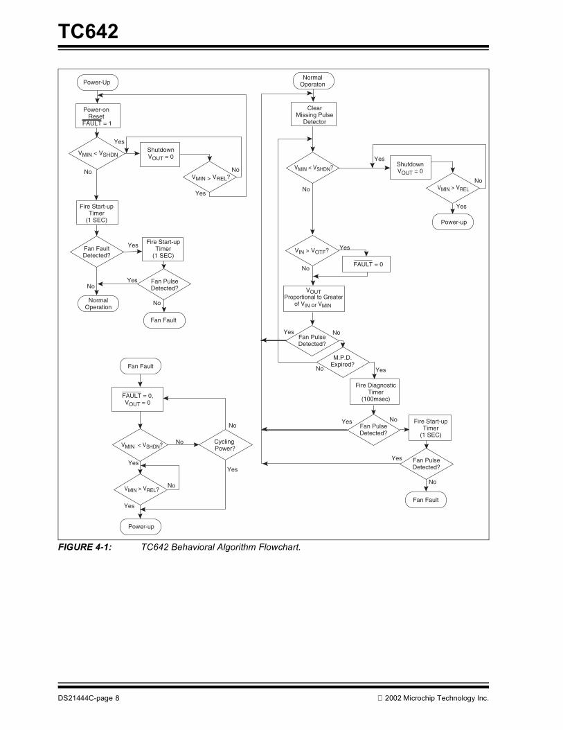
4.0 SYSTEM BEHAVIORThe flowcharts describing the TC642’s behavioralalgorithm are shown in Figure 4-1. They can besummarized as follows:
4.1 Power-Up(1) Assuming the device is not being held in shutdown
mode (VMIN > VREL)…
(2) Turn VOUT output on for 32 cycles of the PWMclock. This ensures that the fan will start from adead stop.
(3) During this Start-up Timer, if a fan pulse isdetected, branch to Normal Operation; if none arereceived…
(4) Activate the 32-cycle Start-up Timer one moretime and look for a fan pulse; if a fan pulse isdetected, proceed to Normal Operation; if noneare received…
(5) Proceed to Fan Fault.
(6) End.
4.2 Normal OperationNormal Operation is an endless loop which may onlybe exited by entering shutdown mode or Fan Fault. Theloop can be thought of as executing at the frequency ofthe oscillator and PWM. (1) Reset the missing pulse detector.(2) Is TC642 in shutdown? If so…
a. VOUT duty cycle goes to zero.b. FAULT is disabled.c. Exit the loop and wait for VMIN > VREL to
(3) If an over-temperature fault occurs (VIN > VOTF),activate FAULT; release FAULT when VIN < VOTF.
(4) Drive VOUT to a duty cycle proportional to thegreater of VIN and VMIN on a cycle by cycle basis.
(5) If a fan pulse is detected, branch back to the startof the loop (1).
(6) If the missing pulse detector times out …
(7) Activate the 3-cycle Diagnostic Timer and look forpulses; if a fan pulse is detected, branch back to the start of the loop (1); if none are received…
(8) Activate the 32-cycle Start-up Timer and look forpulses; if a fan pulse is detected, branch back tothe start of the loop (1); if none are received…
(9) Quit Normal Operation and go to Fan Fault.
(10) End.
4.3 Fan FaultFan fault is an infinite loop wherein the TC642 islatched in shutdown mode. This mode can only bereleased by a reset (i.e., VMIN being brought belowVSHDN, then above VREL, or by power-cycling). (1) While in this state, FAULT is latched on (low) and
the VOUT output is disabled.(2) A reset sequence applied to the VMIN pin will exit
the loop to Power-Up.
(3) End.
2002 Microchip Technology Inc. DS21444C-page 7
TC642
FIGURE 4-1: TC642 Behavioral Algorithm Flowchart.
FAULT = 0,VOUT = 0
Cycling Power?VMIN < VSHDN?
Yes
Yes
Yes
No
No
Fan Fault
Power-up
VMIN > VREL?
Fan FaultDetected?
Fan PulseDetected?
VMIN < VSHDNShutdownVOUT = 0
Yes
No
No
Yes
Yes
Power-Up
NormalOperation
Fan Fault
YES
Power-on Reset
FAULT = 1
VMIN > VREL?No
Fire Start-upTimer
(1 SEC)
Fire Start-upTimer
(1 SEC)
VMIN > VREL
Yes
Fan Fault
ClearMissing Pulse
Detector
VOUTProportional to Greater
of VIN or VMIN
VMIN < VSHDN?
VIN > VOTF?
M.P.D.Expired?
Fan PulseDetected?
No
No
No
No
No
No
Yes
Yes
Yes
NormalOperaton
Power-up
Yes
FAULT = 0
Yes
Fire DiagnosticTimer
(100msec)
Fan PulseDetected?
Fan PulseDetected?
Fire Start-upTimer
(1 SEC)
Yes
No
ShutdownVOUT = 0
No
Yes
No
DS21444C-page 8 2002 Microchip Technology Inc.
TC642
5.0 TYPICAL APPLICATIONSDesigning with the TC642 involves the following:
(1) The temp sensor network must be configured todeliver 1.25V to 2.65V on VIN for 0% to 100% of the temperature range to be regulated.
(2) The minimum fan speed (VMIN) must be set.(3) The output drive transistor and associated circuitry
must be selected.
(4) The SENSE network, RSENSE and CSENSE, mustbe designed for maximum efficiency, whiledelivering adequate signal amplitude.
(5) If shutdown capability is desired, the drive require-ments of the external signal or circuit must be considered.
The TC642 demonstration and prototyping board(TC642DEMO), and the TC642 Evaluation Kit(TC642EV), provide working examples of TC642 cir-cuits and prototyping aids. The TC642DEMO is aprinted circuit board optimized for small size and easeof inclusion into system prototypes. The TC642EV is alarger board intended for benchtop development andanalysis. At the very least, anyone contemplating adesign using the TC642 should consult the documen-tation for both TC642EV (DS21403) and TC642DEMO(DS21401).
FIGURE 5-1: Typical Application Circuit.
5.1 Temperature Sensor DesignThe temperature signal connected to VIN must output avoltage in the range of 1.25V to 2.65V (typical) for 0%to 100% of the temperature range of interest. Thecircuit in Figure 5-2 illustrates a convenient way toprovide this signal. Figure 5-2 shows a simple temperature dependentvoltage divider circuit. RT1 is a conventional NTC ther-mistor while R1 and R2 are standard resistors. The sup-ply voltage, VDD, is divided between R2 and the parallelcombination of RT1 and R1 (for convenience, the paral-lel combination of RT1 and R1 will be referred to asRTEMP). The resistance of the thermistor at varioustemperatures is obtained from the manufacturer’sspecifications. Thermistors are often referred to interms of their resistance at 25°C.
FIGURE 5-2: Temperature Sensing Circuit.Generally, the thermistor shown in Figure 5-2 is a non-linear device with a negative temperature coefficient(also called an NTC thermistor). In Figure 5-2, R1 isused to linearize the thermistor temperature response,while R2 is used to produce a positive temperaturecoefficient at the VIN node. As an added benefit, thisconfiguration produces an output voltage delta of 1.4V,which is well within the range of the VC(SPAN)specification of the TC642. A 100 kΩ NTC thermistor isselected for this application in order to keep IDIV at aminimum.For the voltage range at VIN to be equal to 1.25V to2.65V, the temperature range of this configuration is0°C to 50°C. If a different temperature range is requiredfrom this circuit, R1 should be chosen to equal theresistance value of the thermistor at the center of thisnew temperature range. With this change, R2 isadjusted according to the formulas below. It issuggested that a maximum temperature range of 50°Cbe used with this circuit due to thermistor linearitylimitations.The following two equations permit solving for the twounknown variables, R1 and R2. More informationregarding thermistors can be found in AN679, “Temper-ature Sensing Technologies”, and AN685, “Thermistorsin Single Supply Temperature Sensing Circuits”, whichcan be downloaded from Microchip’s web site at:www.microchip.com.
EQUATION
5.2 Minimum Fan SpeedA voltage divider on VMIN sets the minimum PWM dutycycle and, thus, the minimum fan speed. As with theVIN input, 1.25V to 2.65V typically corresponds to 0%to 100% duty cycle. Assuming that fan speed is linearlyrelated to duty cycle, the minimum speed voltage isgiven by the equation:
EQUATION
For example, if 2500 RPM equates to 100% fan speed, and a minimum speed of 1000 RPM is desired, then the VMIN voltage is:
EQUATION
The VMIN voltage may be set using a simple resistordivider, as shown in Figure 5-3. Per Section 1.0,“Electrical Characteristics”, the leakage current at theVMIN pin is no more than 1 µA. It would be veryconservative to design for a divider current, IDIV, of100 µA. If VDD = 5.0V then;
EQUATION
FIGURE 5-3: VIN Circuit.
R2 = 23.2 kΩ
R1 = 100 kΩ
NTC Thermistor100 kΩ @ 25˚C
RT1
IDIV
VIN
VDD
VDD x R2
RTEMP (T1) + R2= V(T1)
RTEMP (T2) + R2= V(T2)
VDD x R2
Where T1 and T2 are the chosen temperatures andRTEMP is the parallel combination of the thermistorand R1.
Minimum Speed
Full SpeedVMIN = x (1.4) + 1.25V
1000 2500
VMIN = x (1.4) + 1.25V = 1.81V
R1+ R2IDIV = 100µA = , therefore
5.0V
R1 + R2 = = 50,000Ω = 50kΩ100µA5.0V
R2
R1
GND
VDD
VMINIDIV
IIN
DS21444C-page 10 2002 Microchip Technology Inc.
TC642
We can further specify R1 and R2 by the condition thatthe divider voltage is equal to our desired VMIN. Thisyields the following equation:
EQUATION
Solving for the relationship between R1 and R2 resultsin the following equation:
EQUATION
In this example, R1 = (1.762) R2. Substituting this rela-tionship back into the previous equation yields theresistor values:
R2 = 18.1 kΩ, and R1 = 31.9 kΩ
In this case, the standard values of 31.6 kΩ and18.2 kΩ are very close to the calculated values andwould be more than adequate.
5.3 Operations at Low Duty CycleOne boundary condition which may impact the selec-tion of the minimum fan speed is the irregular activationof the Diagnostic Timer due to the TC642 “missing” fancommutation pulses at low speeds. This is a naturalconsequence of low PWM duty cycles (typically 25% orless). Recall that the SENSE function detects commu-tation of the fan as disturbances in the current throughRSENSE. These can only occur when the fan is ener-gized (i.e., VOUT is “on”). At very low duty cycles, theVOUT output is “off” most of the time. The fan may berotating normally, but the commutation events areoccurring during the PWM’s off-time.
The phase relationship between the fan’s commutationand the PWM edges tends to “walk around” as thesystem operates. At certain points, the TC642 may failto capture a pulse within the 32-cycle missing pulsedetector window. When this happens, the 3-cycleDiagnostic Timer will be activated, the VOUT output willbe active continuously for three cycles and, if the fan isoperating normally, a pulse will be detected. If all iswell, the system will return to normal operation. Thereis no harm in this behavior, but it may be audible to theuser as the fan accelerates briefly when the DiagnosticTimer fires. For this reason, it is recommended thatVMIN be set no lower than 1.8V.
5.4 FanSense Network (RSENSE and CSENSE)
The FanSense network, comprised of RSENSE andCSENSE, allows the TC642 to detect commutation ofthe fan motor (FanSense technology). This networkcan be thought of as a differentiator and thresholddetector. The function of RSENSE is to convert the fancurrent into a voltage. CSENSE serves to AC-couple thisvoltage signal and provide a ground-referenced input tothe SENSE pin. Designing a proper SENSE network issimply a matter of scaling RSENSE to provide the nec-essary amount of gain (i.e., the current-to-voltage con-version ratio). A 0.1 µF ceramic capacitor isrecommended for CSENSE. Smaller values requirelarger sense resistors, and higher value capacitors arebulkier and more expensive. Using a 0.1 µF capacitorresults in reasonable values for RSENSE. Figure 5-4illustrates a typical SENSE network. Figure 5-5 showsthe waveforms observed using a typical SENSE net-work.
FIGURE 5-4: SENSE Network.
FIGURE 5-5: SENSE Waveforms.
VDD x R2
R1 + R2VMIN =
VDD - VMIN
VMIN R1 = R2 x
Q1
GND
VDD
RSENSE
SENSE
RBASE
CSENSE(0.1 µF Typ.)
VOUT
Fan
1
Ch1 100mV
Tek Run: 10.0kS/s Sample
Ch2 100mV M5.00ms Ch1 142mV
GND
[ T ]
T
Waveform @ Sense Resistor
90mV50mVGND
Waveform @ Sense Pin
2
2002 Microchip Technology Inc. DS21444C-page 11
TC642
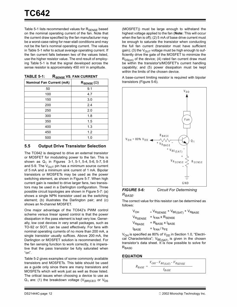
Table 5-1 lists recommended values for RSENSE basedon the nominal operating current of the fan. Note thatthe current draw specified by the fan manufacturer maybe a worst-case rating for near-stall conditions and maynot be the fan’s nominal operating current. The valuesin Table 5-1 refer to actual average operating current. Ifthe fan current falls between two of the values listed,use the higher resistor value. The end result of employ-ing Table 5-1 is that the signal developed across thesense resistor is approximately 450 mV in amplitude.
TABLE 5-1: RSENSE VS. FAN CURRENT
5.5 Output Drive Transistor SelectionThe TC642 is designed to drive an external transistoror MOSFET for modulating power to the fan. This isshown as Q1 in Figures 3-1, 5-1, 5-4, 5-6, 5-7, 5-8and 5-9. The VOUT pin has a minimum source currentof 5 mA and a minimum sink current of 1 mA. Bipolartransistors or MOSFETs may be used as the powerswitching element, as shown in Figure 5-7. When highcurrent gain is needed to drive larger fans, two transis-tors may be used in a Darlington configuration. Threepossible circuit topologies are shown in Figure 5-7: (a)shows a single NPN transistor used as the switchingelement; (b) illustrates the Darlington pair; and (c)shows an N-channel MOSFET.
One major advantage of the TC642’s PWM controlscheme versus linear speed control is that the powerdissipation in the pass element is kept very low. Gener-ally, low cost devices in very small packages, such asTO-92 or SOT, can be used effectively. For fans withnominal operating currents of no more than 200 mA, asingle transistor usually suffices. Above 200 mA, theDarlington or MOSFET solution is recommended. Forthe fan sensing function to work correctly, it is impera-tive that the pass transistor be fully saturated when“on”.
Table 5-2 gives examples of some commonly availabletransistors and MOSFETs. This table should be usedas a guide only since there are many transistors andMOSFETs which will work just as well as those listed.The critical issues when choosing a device to use asQ1 are: (1) the breakdown voltage (V(BR)CEO or VDS
(MOSFET)) must be large enough to withstand thehighest voltage applied to the fan (Note: This will occurwhen the fan is off); (2) 5 mA of base drive current mustbe enough to saturate the transistor when conductingthe full fan current (transistor must have sufficientgain); (3) the VOUT voltage must be high enough to suf-ficiently drive the gate of the MOSFET to minimize theRDS(on) of the device; (4) rated fan current draw mustbe within the transistor's/MOSFET's current handlingcapability; and (5) power dissipation must be keptwithin the limits of the chosen device.
A base-current limiting resistor is required with bipolartransistors (Figure 5-6).
FIGURE 5-6: Circuit For Determining RBASE.The correct value for this resistor can be determined asfollows:
VOH is specified as 80% of VDD in Section 1.0, “Electri-cal Characteristics”; VBE(SAT) is given in the chosentransistor’s data sheet. It is now possible to solve forRBASE.
Some applications require the fan to be powered fromthe negative 12V supply to keep motor noise out of thepositive voltage power supplies. As is shown inFigure 5-8, zener diode D1 offsets the -12V power sup-ply voltage, holding transistor Q1 off when VOUT is low.
When VOUT is high, the voltage at the anode of D1increases by VOUT, causing Q1 to turn on. Operation isotherwise consistent with the case of fan operationfrom +12V.
*Note: Value depends on the specific application and is shown for example only.
2002 Microchip Technology Inc. DS21444C-page 13
TC642
TABLE 5-2: TRANSISTORS AND MOSFETS FOR Q1 (VDD = 5V)
5.6 Latch-up Considerations As with any CMOS IC, the potential exists for latch-upif signals are applied to the device which are outsidethe power supply range. This is of particular concernduring power-up if the external circuitry (such as thesensor network, VMIN divider or shutdown circuit) ispowered by a supply different from that of the TC642.Care should be taken to ensure that the TC642’s VDDsupply powers up first. If possible, the networksattached to VIN and VMIN should connect to the VDDsupply at the same physical location as the IC itself.Even if the IC and any external networks are poweredby the same supply, physical separation of theconnecting points can result in enough parasiticcapacitance and/or inductance in the power supplyconnections to delay one power supply “routing” versusanother.
Device Package Max. VBE(sat)/VGS(V) Min. HFE
VCEO/VDS(V)
Fan Current (mA)
SuggestedRBASE (Ω)
MMBT2222A SOT-23 1.2 50 40 150 800MPS2222A TO-92 1.2 50 40 150 800MPS6602 TO-92 1.2 50 40 500 301SI2302 SOT-23 2.5 NA 20 500 Note 1MGSF1N02E SOT-23 2.5 NA 20 500 Note 1SI4410 SO-8 4.5 NA 30 1000 Note 1SI2308 SOT-23 4.5 NA 60 500 Note 1Note 1: A series gate resistor may be used in order to control the MOSFET turn-on and turn-off times.
DS21444C-page 14 2002 Microchip Technology Inc.
TC642
5.7 Power Supply Routing and
BypassingNoise present on the VIN and VMIN inputs may causeerroneous operation of the FAULT output. As a result,these inputs should be bypassed with a 0.01 µFcapacitor mounted as close to the package as is possi-ble. This is particularly true of VIN, which is usuallydriven from a high impedance source (such as a ther-mistor). In addition, the VDD input should be bypassedwith a 1 µF capacitor. Grounds should be kept as shortas possible. To keep fan noise off the TC642 groundpin, individual ground returns for the TC642 and the lowside of the fan current sense resistor should be used.
Design Example Step 1. Calculate R1 and R2 based on using an NTC
having a resistance of 10 kΩ at TMIN (25°C)and 4.65 kΩ at TMAX (45°C) (see Figure 5-9).R1 = 20.5 kΩR2 = 3.83 kΩ
Step 2. Set minimum fan speed VMIN = 1.8V. Limit the divider current to 100 µA from which R5 = 33 kΩ and R6 = 18 kΩ.
Step 3. Design the output circuit.Maximum fan motor current = 250 mA. Q1 beta is chosen at 50 from which R7 = 800 Ω.
FIGURE 5-9: Design Example.
FAULT
SENSE
NTC10 kΩ @ 25˚C
R120.5 kΩ
R23.83 kΩ
R533 kΩ
R7800Ω
R618 kΩR8
10 kΩ
GND
FanShutdown
(Optional)
Q1
Q2
+12V
+5V
+5V
+5V
VDDVIN
VMIN
VOUT
RSENSE2.2Ω
CSENSE0.1 µF
C11µF
CF
TC642
Fan
CB0.01 µF
CB 0.01 µF
+CB1 µF
8 4
6
7
5
2
3
1
Fan/ Thermal Fault
2002 Microchip Technology Inc. DS21444C-page 15
TC642
5.8 TC642 as a Microcontroller
PeripheralIn a system containing a microcontroller or other hostintelligence, the TC642 can be effectively managed asa CPU peripheral. Routine fan control functions can beperformed by the TC642 without processor intervention.The microcontroller receives temperature data from oneor more points throughout the system. It calculates a fanoperating speed based on an algorithm specificallydesigned for the application at hand. The processorcontrols fan speed using complementary port bits I/O1through I/O3. Resistors R1 through R6 (5% tolerance)form a crude 3-bit DAC that translates the 3-bit code
from the processor's outputs into a 1.6V DC control sig-nal. A monolithic DAC or digital pot may be usedinstead of the circuit shown in Figure 5-10.With VMIN set to 1.8V, the TC642 has a minimumoperating speed of approximately 40% of full ratedspeed when the processor's output code is 000[B].Output codes 001[B] to 111[B] operate the fan fromroughly 40% to 100% of full speed. An open-drainoutput from the processor (I/O0) can be used to resetthe TC642 following detection of a fault condition. TheFAULT output can be connected to the processor'sinterrupt input, or to an I/O pin, for polled operation.
FIGURE 5-10: TC642 as a Microcontroller Peripheral.
TC642
VIN
CF
VMIN
GND
VDD
VOUT
FAULT
SENSE
(Optional)
(MSB)R1
110 kΩ
R2240 kΩ
R3360 kΩ
(LSB)R5
1.5 kΩ+5V
R61 kΩ
R418 kΩ
R733 kΩ
+5VR8
18 kΩ
CB.01 µF
+
1 µF
CB.01 µF
Fan
+12V
+5V
CB1 µF
+
800Ω
+5VR10
10 kΩ
0.1 µF
2N2222A
R112.2Ω
1
2
3
4 5
6
7
8
(RESET)
CMOSMicrocontroller
+5V
Analog or DigitalTemperature
Data from one ormore Sensors
I/O0
I/O1
I/O2
I/O3
INTGND
CMOSOutputs
Open-drain Outputs
R9
DS21444C-page 16 2002 Microchip Technology Inc.
TC642
6.0 PACKAGING INFORMATION
6.1 Package Marking Information
XXXXXXXXNNN
YYWW
8-Lead PDIP (300 mil) Example:
8-Lead SOIC (150 mil) Example:
XXXXXXXXYYWW
NNN
TC642CPA025
0215
TC642COA0215
025
8-Lead MSOP Example:
XXXXXX
YWWNNN
TC642E
215025
Legend: XX...X Customer specific information*YY Year code (last 2 digits of calendar year)WW Week code (week of January 1 is week ‘01’)NNN Alphanumeric traceability code
Note: In the event the full Microchip part number cannot be marked on one line, it willbe carried over to the next line thus limiting the number of available charactersfor customer specific information.
* Standard marking consists of Microchip part number, year code, week code, traceability code (facilitycode, mask rev#, and assembly code). For marking beyond this, certain price adders apply. Please checkwith your Microchip Sales Office.
2002 Microchip Technology Inc. DS21444C-page 17
TC642
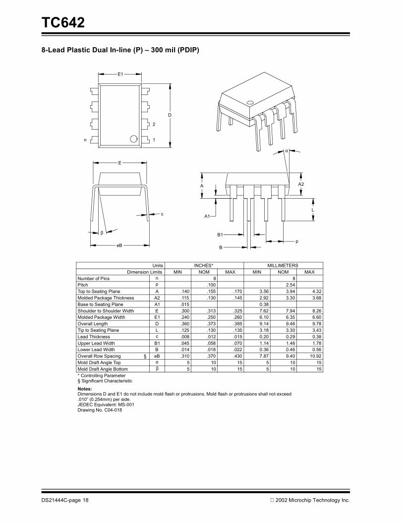
8-Lead Plastic Dual In-line (P) – 300 mil (PDIP)
B1
B
A1
A
L
A2
p
α
E
eB
β
c
E1
n
D
1
2
Units INCHES* MILLIMETERSDimension Limits MIN NOM MAX MIN NOM MAX
Number of Pins n 8 8Pitch p .100 2.54Top to Seating Plane A .140 .155 .170 3.56 3.94 4.32Molded Package Thickness A2 .115 .130 .145 2.92 3.30 3.68Base to Seating Plane A1 .015 0.38Shoulder to Shoulder Width E .300 .313 .325 7.62 7.94 8.26Molded Package Width E1 .240 .250 .260 6.10 6.35 6.60Overall Length D .360 .373 .385 9.14 9.46 9.78Tip to Seating Plane L .125 .130 .135 3.18 3.30 3.43Lead Thickness c .008 .012 .015 0.20 0.29 0.38Upper Lead Width B1 .045 .058 .070 1.14 1.46 1.78Lower Lead Width B .014 .018 .022 0.36 0.46 0.56Overall Row Spacing § eB .310 .370 .430 7.87 9.40 10.92Mold Draft Angle Top α 5 10 15 5 10 15Mold Draft Angle Bottom β 5 10 15 5 10 15* Controlling Parameter
Notes:Dimensions D and E1 do not include mold flash or protrusions. Mold flash or protrusions shall not exceed
JEDEC Equivalent: MS-001Drawing No. C04-018
.010” (0.254mm) per side.
§ Significant Characteristic
DS21444C-page 18 2002 Microchip Technology Inc.
TC642
8-Lead Plastic Small Outline (SN) – Narrow, 150 mil (SOIC)
Foot Angle f 0 4 8 0 4 8
1512015120βMold Draft Angle Bottom1512015120αMold Draft Angle Top
Notes:Dimensions D and E1 do not include mold flash or protrusions. Mold flash or protrusions shall not exceed .010” (0.254mm) per side.JEDEC Equivalent: MS-012Drawing No. C04-057
§ Significant Characteristic
2002 Microchip Technology Inc. DS21444C-page 19
TC642
8-Lead Plastic Micro Small Outline Package (MS) (MSOP)
p
A
A1
A2
D
L
c
Dimensions D and E1 do not include mold flash or protrusions. Mold flash or protrusions shall not
.037.035FFootprint (Reference)
exceed. 010" (0.254mm) per side.
Notes:
Drawing No. C04-111
*Controlling Parameter
Mold Draft Angle TopMold Draft Angle Bottom
Foot Angle
Lead WidthLead Thickness
βα
cB
φ
77
.004
.010
0.006.012
(F)
β
Dimension Limits
Overall HeightMolded Package Thickness
Molded Package WidthOverall LengthFoot Length
Standoff §Overall Width
Number of PinsPitch
A
L
E1D
A1E
A2
.016
.114
.114.022
.118
.118
.002
.030
.193
.034
MIN
pn
Units
.026
NOM8
INCHES
1.000.950.90.039
0.150.30
.008
.016
60.100.25
0
77
0.200.40
6
MILLIMETERS*
0.65
0.86
3.003.000.55
4.90
.044
.122
.028
.122
.038
.006
0.40
2.902.90
0.050.76
MINMAX NOM
1.18
0.70
3.103.10
0.150.97
MAX8
α
E1
E
Bn 1
2
φ
§ Significant Characteristic
.184 .200 4.67 .5.08
DS21444C-page 20 2002 Microchip Technology Inc.
TC642
6.2 Taping Form
Component Taping Orientation for 8-Pin SOIC (Narrow) Devices
Package Carrier Width (W) Pitch (P) Part Per Full Reel Reel Size
8-Pin SOIC (N) 12 mm 8 mm 2500 13 in
Carrier Tape, Number of Components Per Reel and Reel Size
Standard Reel Component Orientationfor 713 Suffix Device
PIN 1
User Direction of Feed
P
W
Component Taping Orientation for 8-Pin MSOP Devices
Package Carrier Width (W) Pitch (P) Part Per Full Reel Reel Size
8-Pin MSOP 12 mm 8 mm 2500 13 in
Carrier Tape, Number of Components Per Reel and Reel Size
PIN 1
User Direction of Feed
Standard Reel Component Orientationfor 713 Suffix Device
W
P
2002 Microchip Technology Inc. DS21444C-page 21
TC642
NOTES:
DS21444C-page 22 2002 Microchip Technology Inc.
TC642
ON-LINE SUPPORTMicrochip provides on-line support on the MicrochipWorld Wide Web site.
The web site is used by Microchip as a means to makefiles and information easily available to customers. Toview the site, the user must have access to the Internetand a web browser, such as Netscape® or Microsoft®Internet Explorer. Files are also available for FTPdownload from our FTP site.
Connecting to the Microchip Internet Web Site The Microchip web site is available at the followingURL:
www.microchip.comThe file transfer site is available by using an FTP ser-vice to connect to:
ftp://ftp.microchip.comThe web site and file transfer site provide a variety ofservices. Users may download files for the latestDevelopment Tools, Data Sheets, Application Notes,User's Guides, Articles and Sample Programs. A vari-ety of Microchip specific business information is alsoavailable, including listings of Microchip sales offices,distributors and factory representatives. Other dataavailable for consideration is:• Latest Microchip Press Releases• Technical Support Section with Frequently Asked
Questions • Design Tips• Device Errata• Job Postings• Microchip Consultant Program Member Listing• Links to other useful web sites related to
Microchip Products• Conferences for products, Development Systems,
technical information and more• Listing of seminars and events
2002 Microchip Technology Inc.
SYSTEMS INFORMATION AND UPGRADE HOT LINE The Systems Information and Upgrade Line providessystem users a listing of the latest versions of all ofMicrochip's development systems software products.Plus, this line provides information on how customerscan receive the most current upgrade kits.The Hot LineNumbers are: 1-800-755-2345 for U.S. and most of Canada, and
1-480-792-7302 for the rest of the world.
092002
DS21444C-page23
TC642
READER RESPONSEIt is our intention to provide you with the best documentation possible to ensure successful use of your Microchip prod-uct. If you wish to provide your comments on organization, clarity, subject matter, and ways in which our documentationcan better serve you, please FAX your comments to the Technical Publications Manager at (480) 792-4150.
Please list the following information, and use this outline to provide us with your comments about this document.
1. What are the best features of this document?
2. How does this document meet your hardware and software development needs?
3. Do you find the organization of this document easy to follow? If not, why?
4. What additions to the document do you think would enhance the structure and subject?
5. What deletions from the document could be made without affecting the overall usefulness?
6. Is there any incorrect or misleading information (what and where)?
PRODUCT IDENTIFICATION SYSTEMTo order or obtain information, e.g., on pricing or delivery, refer to the factory or the listed sales office.
Sales and SupportData SheetsProducts supported by a preliminary Data Sheet may have an errata sheet describing minor operational differences and recom-mended workarounds. To determine if an errata sheet exists for a particular device, please contact one of the following:
1. Your local Microchip sales office2. The Microchip Corporate Literature Center U.S. FAX: (480) 792-72773. The Microchip Worldwide Site (www.microchip.com)
Please specify which device, revision of silicon and Data Sheet (include Literature #) you are using.
New Customer Notification SystemRegister on our web site (www.microchip.com/cn) to receive the most current information on our products.
PART NO. X /XX
PackageTemperatureRange
Device
Device: TC642: PWM Fan Speed Controller w/ Fault Detection
Temperature Range: C = 0°C to +70°CV = 0°C to +85°CE = -40°C to +85°C
Package: PA = Plastic DIP (300 mil Body), 8-lead *OA = Plastic SOIC, (150 mil Body), 8-leadUA = Plastic Micro Small Outline (MSOP), 8-lead **
* PDIP is only offered in the C and V temp ranges** MSOP is only available in the V and E temp ranges
Examples:a) TC642COA: PWM Fan Speed Controller w/
Fault Detection, SOIC package.b) TC642COA713: PWM Fan Speed Controller
w/ Fault Detection, SOIC package, Tape andReel.
c) TC642CPA: PWM Fan Speed Controller w/Fault Detection, PDIP package.
d) TC642EUA: PWM Fan Speed Controller w/Fault Detection, MSOP package.
2002 Microchip Technology Inc. DS21444C-page25
TC642
NOTES:
DS21444C-page 26 2002 Microchip Technology Inc.
Information contained in this publication regarding deviceapplications and the like is intended through suggestion onlyand may be superseded by updates. It is your responsibility toensure that your application meets with your specifications.No representation or warranty is given and no liability isassumed by Microchip Technology Incorporated with respectto the accuracy or use of such information, or infringement ofpatents or other intellectual property rights arising from suchuse or otherwise. Use of Microchip’s products as critical com-ponents in life support systems is not authorized except withexpress written approval by Microchip. No licenses are con-veyed, implicitly or otherwise, under any intellectual propertyrights.
2002 Microchip Technology Inc.
Trademarks
The Microchip name and logo, the Microchip logo, KEELOQ,MPLAB, PIC, PICmicro, PICSTART and PRO MATE areregistered trademarks of Microchip Technology Incorporatedin the U.S.A. and other countries.
FilterLab, microID, MXDEV, MXLAB, PICMASTER, SEEVALand The Embedded Control Solutions Company areregistered trademarks of Microchip Technology Incorporatedin the U.S.A.
dsPIC, dsPICDEM.net, ECONOMONITOR, FanSense,FlexROM, fuzzyLAB, In-Circuit Serial Programming, ICSP,ICEPIC, microPort, Migratable Memory, MPASM, MPLIB,MPLINK, MPSIM, PICC, PICDEM, PICDEM.net, rfPIC, SelectMode and Total Endurance are trademarks of MicrochipTechnology Incorporated in the U.S.A. and other countries.
Serialized Quick Turn Programming (SQTP) is a service markof Microchip Technology Incorporated in the U.S.A.
All other trademarks mentioned herein are property of theirrespective companies.
Microchip received QS-9000 quality system certification for its worldwide headquarters, design and wafer fabrication facilities in Chandler and Tempe, Arizona in July 1999 and Mountain View, California in March 2002. The Company’s quality system processes and procedures are QS-9000 compliant for its PICmicro® 8-bit MCUs, KEELOQ® code hopping devices, Serial EEPROMs, microperipherals, non-volatile memory and analog products. In addition, Microchip’s quality system for the design and manufacture of development systems is ISO 9001 certified.
DS21444C-page 28 2002 Microchip Technology Inc.
MAMERICASCorporate Office2355 West Chandler Blvd.Chandler, AZ 85224-6199Tel: 480-792-7200 Fax: 480-792-7277Technical Support: 480-792-7627Web Address: http://www.microchip.comRocky Mountain2355 West Chandler Blvd.Chandler, AZ 85224-6199Tel: 480-792-7966 Fax: 480-792-4338
Atlanta500 Sugar Mill Road, Suite 200BAtlanta, GA 30350Tel: 770-640-0034 Fax: 770-640-0307Boston2 Lan Drive, Suite 120Westford, MA 01886Tel: 978-692-3848 Fax: 978-692-3821Chicago333 Pierce Road, Suite 180Itasca, IL 60143Tel: 630-285-0071 Fax: 630-285-0075Dallas4570 Westgrove Drive, Suite 160Addison, TX 75001Tel: 972-818-7423 Fax: 972-818-2924DetroitTri-Atria Office Building 32255 Northwestern Highway, Suite 190Farmington Hills, MI 48334Tel: 248-538-2250 Fax: 248-538-2260Kokomo2767 S. Albright Road Kokomo, Indiana 46902Tel: 765-864-8360 Fax: 765-864-8387Los Angeles18201 Von Karman, Suite 1090Irvine, CA 92612Tel: 949-263-1888 Fax: 949-263-1338New York150 Motor Parkway, Suite 202Hauppauge, NY 11788Tel: 631-273-5305 Fax: 631-273-5335San JoseMicrochip Technology Inc.2107 North First Street, Suite 590San Jose, CA 95131Tel: 408-436-7950 Fax: 408-436-7955Toronto6285 Northam Drive, Suite 108Mississauga, Ontario L4V 1X5, CanadaTel: 905-673-0699 Fax: 905-673-6509