26
QCVS SerDes Tool User Guide NXP Semiconductors Document Number: QCVS_SerDes_User_Guide User's Guide Rev. 4.x, 05/2016
QCVS SerDes Tool User Guide
NXP Semiconductors Document Number: QCVS_SerDes_User_Guide
User's Guide Rev. 4.x, 05/2016

Contents
Chapter 1 SerDes Configuration and Validation.......................................... 31.1 Introduction.......................................................................................................................... 3
1.1.1 Acronyms............................................................................................................................... 31.1.2 SerDes hardware block challenges........................................................................................41.1.3 Creating a SerDes project......................................................................................................41.1.4 Working with SerDes components.........................................................................................5
1.2 SerDes configuration............................................................................................................61.2.1 Module Overview pane..........................................................................................................71.2.2 Lane Configuration pane....................................................................................................... 71.2.3 PLL Configuration pane.........................................................................................................81.2.4 Protocol/Speed Configuration window...................................................................................91.2.5 Configuration Registers view............................................................................................... 121.2.6 Errata support......................................................................................................................13
1.3 SerDes validation............................................................................................................... 141.3.1 SerDes Validation pane.......................................................................................................151.3.2 Data generation modes....................................................................................................... 151.3.3 SerDes validation scenarios................................................................................................17
1.3.3.1 BIST scenario........................................................................................................................171.3.3.2 Tx pattern generation scenario..............................................................................................181.3.3.3 Jitter scope scenario..............................................................................................................19
1.3.4 SerDes validation best practices......................................................................................... 211.3.5 Target connection settings...................................................................................................22
1.4 How to use a SerDes configuration....................................................................................221.4.1 RCW settings...................................................................................................................... 231.4.2 Code generation..................................................................................................................231.4.3 Synchronization between SerDes and PBL........................................................................ 23
1.5 Licensing............................................................................................................................ 24
Index....................................................................................................................................25
Contents
QCVS SerDes Tool User Guide, Rev. 4.x, 05/20162 NXP Semiconductors
Chapter 1SerDes Configuration and Validation
This document describes the capabilities of the SerDes configuration and validation tool (SerDes stands for Serializer/Deserializer) for the QorIQ devices.
The SerDes tool is a part of the QorIQ Configuration and Validation Suite (QCVS) product.
This chapter contains the following sections:
• Introduction on page 3
• SerDes configuration on page 6
• SerDes validation on page 14
• How to use a SerDes configuration on page 22
• Licensing on page 24
1.1 IntroductionThe SerDes tool allows you to configure the SerDes block and provides you a GUI application to validate the configuration.
You can start with a default and arbitrary configuration or connect to your board and read its current SerDes configuration.The validation features of the tool allows you to exercise the SerDes built-in test capabilities (for example, BIST, Jitter scope,and Tx pattern generation) and view the results. The validation features are licensed. For more details, see Licensing onpage 24.
The SerDes tool supports numerous QorIQ devices. See QCVS Release Notes for details on which QorIQ SoCs aresupported by the SerDes tool.
This section contains the following subsections:
• Acronyms on page 3
• SerDes hardware block challenges on page 4
• Creating a SerDes project on page 4
• Working with SerDes components on page 5
1.1.1 AcronymsThis section provides a list of all the acronyms used in the current document.
Table 1. Acronyms
Acronym Meaning
BIST Built-in self-test
GUI Graphical user interface
Table continues on the next page...
SerDes Configuration and Validation
Introduction
QCVS SerDes Tool User Guide, Rev. 4.x, 05/2016NXP Semiconductors 3

Table 1. Acronyms (continued)
Acronym Meaning
IP Internet protocol
PBL Pre-boot loader
PCIe Peripheral component interconnect express
PLL Phase-locked loop
QCVS QorIQ Configuration and Validation Suite
RCW Reset configuration word
Rx Receive/receiver
SATA Serial advanced technology attachment
SerDes Serializer/Deserializer
SoC System-on-chip
Tx Transmit/transmitter
UI User interface
1.1.2 SerDes hardware block challengesSerDes is a hardware block that is used for high-speed data transmission.
The SerDes hardware block is present in most of the SoCs that need to enable a reliable and high throughput for differenttypes of traffic coming from different peripherals, such as PCIe, SATA, and so on.
Having an optimally configured and validated SerDes block is critical for designing a board successfully. This involves notonly planning what protocols and speeds can and will be used, but also setting that configuration via the RCW. It also involvesconfiguring electrical behaviors of lanes via memory-mapped registers to get reliable and optimal performance. The latterrequires driving traffic through the lanes and analyzing the result. Fortunately, the SerDes blocks on most QorIQ SoCs havecharacterization circuitry to support this, without expensive scope or other testing equipment.
An optimal SerDes configuration is usually obtained by tweaking a configuration, examining the effect on transmission, andrepeating until the best configuration has been identified. The SerDes tool allows doing all this with a rich, user-friendly GUI.
1.1.3 Creating a SerDes projectThe first step to configure or validate SerDes is to create a QCVS project with a SerDes component.
To create a SerDes project, perform these steps:
1. Launch QCVS.
2. Select File > New > QorIQ Configuration Project. The New QorIQ Configuration Project wizard starts, displayingthe Create a QorIQ Configuration Project page.
3. Specify the project name in the Project name text box, and click Next.
4. On the Devices page, choose a device to work with. See QCVS Release Notes for details on which QorIQ SoCs aresupported by the SerDes tool.
5. Now, choose a device revision. If only one revision is available, it is automatically chosen. Click Next to continue.
6. On the Toolset selection page, select SERDES Configuration Tool, and click Next to continue.
SerDes Configuration and Validation
Introduction
QCVS SerDes Tool User Guide, Rev. 4.x, 05/20164 NXP Semiconductors

7. On the SERDES Configuration page, the following two options are available to create a SerDes component (asshown in the next figure):
• Create default configuration: Creates a default SerDes configuration with predefined SerDes settings.
• Read from target: The SerDes configuration will be read from the board you are connected to. If you select thisoption, you also need to perform the following steps:
a. Specify the target connection parameters, including the probe type and connection string.
b. Click the READ FROM TARGET link, and notice if the text box next to the link shows a message indicating thatthe read operation was successful.
Figure 1. Defining SerDes configuration
8. Click Finish to create the project.
When a new project is created, each of the SerDes modules defined for the selected device is represented as a SerDescomponent in the project. The next section shows how to use a SerDes component to configure and validate the SerDesblock.
1.1.4 Working with SerDes componentsWhen a new project is created, the SerDes components are added in the Components view.
The figure below shows four SerDes components added in the Components view. Each component corresponds to oneSerDes module. The T4240 SoC has four SerDes modules. As shown in the figure, all four components are grouped underthe parent SerDes block component.
SerDes Configuration and Validation
Introduction
QCVS SerDes Tool User Guide, Rev. 4.x, 05/2016NXP Semiconductors 5
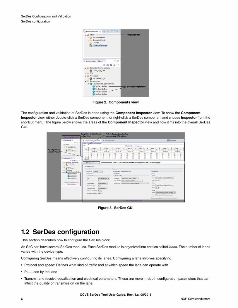
Figure 2. Components view
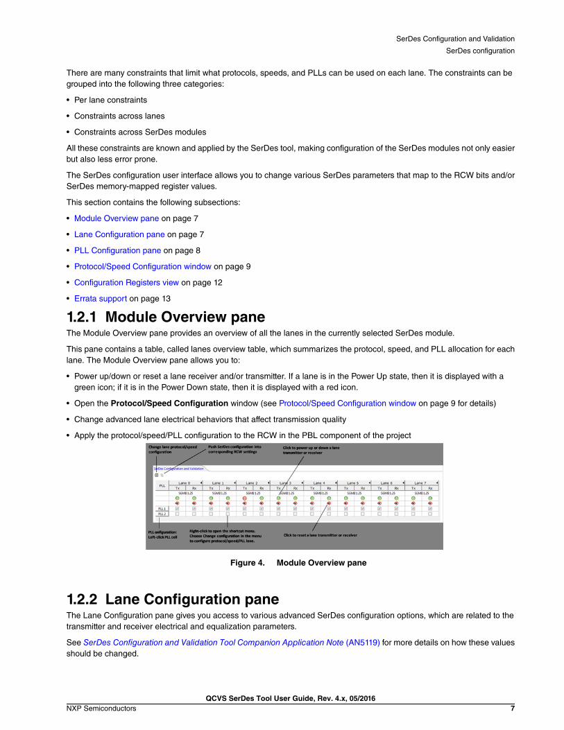
The configuration and validation of SerDes is done using the Component Inspector view. To show the ComponentInspector view, either double-click a SerDes component, or right-click a SerDes component and choose Inspector from theshortcut menu. The figure below shows the areas of the Component Inspector view and how it fits into the overall SerDesGUI.
Figure 3. SerDes GUI
1.2 SerDes configurationThis section describes how to configure the SerDes block.
An SoC can have several SerDes modules. Each SerDes module is organized into entities called lanes. The number of lanesvaries with the device type.
Configuring SerDes means effectively configuring its lanes. Configuring a lane involves specifying:
• Protocol and speed: Defines what kind of traffic and at which speed the lane can operate with
• PLL used by the lane
• Transmit and receive equalization and electrical parameters. These are more in-depth configuration parameters that canaffect the quality of transmission on the lane.
SerDes Configuration and Validation
SerDes configuration
QCVS SerDes Tool User Guide, Rev. 4.x, 05/20166 NXP Semiconductors
There are many constraints that limit what protocols, speeds, and PLLs can be used on each lane. The constraints can begrouped into the following three categories:
• Per lane constraints
• Constraints across lanes
• Constraints across SerDes modules
All these constraints are known and applied by the SerDes tool, making configuration of the SerDes modules not only easierbut also less error prone.
The SerDes configuration user interface allows you to change various SerDes parameters that map to the RCW bits and/orSerDes memory-mapped register values.
This section contains the following subsections:
• Module Overview pane on page 7
• Lane Configuration pane on page 7
• PLL Configuration pane on page 8
• Protocol/Speed Configuration window on page 9
• Configuration Registers view on page 12
• Errata support on page 13
1.2.1 Module Overview paneThe Module Overview pane provides an overview of all the lanes in the currently selected SerDes module.
This pane contains a table, called lanes overview table, which summarizes the protocol, speed, and PLL allocation for eachlane. The Module Overview pane allows you to:
• Power up/down or reset a lane receiver and/or transmitter. If a lane is in the Power Up state, then it is displayed with agreen icon; if it is in the Power Down state, then it is displayed with a red icon.
• Open the Protocol/Speed Configuration window (see Protocol/Speed Configuration window on page 9 for details)
• Change advanced lane electrical behaviors that affect transmission quality
• Apply the protocol/speed/PLL configuration to the RCW in the PBL component of the project
Figure 4. Module Overview pane
1.2.2 Lane Configuration paneThe Lane Configuration pane gives you access to various advanced SerDes configuration options, which are related to thetransmitter and receiver electrical and equalization parameters.
See SerDes Configuration and Validation Tool Companion Application Note (AN5119) for more details on how these valuesshould be changed.
SerDes Configuration and Validation
SerDes configuration
QCVS SerDes Tool User Guide, Rev. 4.x, 05/2016NXP Semiconductors 7

The Lane Configuration pane shows the configuration of a single lane at a time. To configure a lane, click the lane in theModule Overview pane, and then configure it in the Lane Configuration pane (see figure below).
Figure 5. Lane Configuration pane
1.2.3 PLL Configuration paneThis pane allows you to view and modify PLL settings.
The Lane Configuration pane becomes the PLL Configuration pane when a PLL is selected in the Module Overview pane.
Each SerDes lane uses a PLL that is determined by the protocol and speed option described in Protocol/Speed Configurationwindow on page 9. The PLL used by each lane is displayed in the lanes overview table in the Read-Only mode, as shownin the figure below.
Note that for a lane, both Tx and Rx use the same PLL. You can configure a PLL by left-clicking it in the Module Overviewpane. However, you should avoid altering most of these settings, as they are directly tied to what protocol and speed youchose for the module's lanes in the Protocol/Speed Configuration window. In other words, most PLL settings areautomatically updated when you make your protocol and speed choices. Altering PLL settings in this pane can easily leaveyou with a configuration that makes no sense. Therefore, treat this pane as mostly informational.
The figure below shows the PLL allocation per lane, how to access the PLL Configuration pane, and the PLL Configurationpane.
Figure 6. PLL Configuration pane
SerDes Configuration and Validation
SerDes configuration
QCVS SerDes Tool User Guide, Rev. 4.x, 05/20168 NXP Semiconductors

1.2.4 Protocol/Speed Configuration windowThis section describes the functionality and usage of the Protocol/Speed Configuration window.
A QorIQ SoC is capable of simultaneously transmitting and receiving various types of serial traffic at different speeds. Eachlane is an independent traffic path. There are protocol and speed lane constraints within a SerDes module and even acrossmodules. Knowing and observing these constraints becomes difficult when relying strictly on the reference manual or erratadocument of the SoC. For example, answering the questions "Can my SoC support PCIe Gen 3, XFI, and SATA trafficsimultaneously?" and "If so, how do I configure the SerDes blocks for that" becomes very difficult by looking at the SoCdocumentation. QCVS makes it easy. With the SerDes tool, the answers and configurations are a few mouse clicks away.
The Protocol/Speed Configuration window allows you to choose the protocols and speeds for the lanes in all your SerDesmodules. In an ideal world, you could choose any protocol and speed for each lane. In reality, only a few protocols and speedsare supported for each lane. Moreover, choosing a protocol/speed for one lane typically dictates or restricts the protocols andspeeds on some or all of the other lanes in the SerDes module. In some cases, it can even restrict what you can use in otherSerDes modules. The end result is that for each SerDes module, you have a limited number of combinations and permutationsof protocols and speeds. A SerDes module is configured to use a particular combination/permutation out of reset viaRCW[SRDS_PRTCL_Sn]. The values for these RCW fields (that is, the combinations and permutations available) aretypically represented in tables in the SoC reference manual. The table below shows an example from LS2085A ReferenceManual.
Table 2. SRDS_PRCTL choices for SerDes2 in LS2085A Reference Manual
SRDS_PRCTL_S2
A B C D E F G H PLLmapping
hex SD2[0] SD2[1] SD2[2] SD2[3] SD2[4] SD2[5] SD2[6] SD2[7] A-H
07 SG9 SG10 SG11 SG12 SG13 SG14 SG15 SG16 22222222
09 SG9 SG10 SG11 SG12 SG13 SG14 SG15 SG16 11111111
0A SG9 SG10 SG11 SG12 SG13 SG14 SG15 SG16 22221111
0C SG9 SG10 SG11 SG12 SG13 SG14 SG15 SG16 11112222
0E SG9 SG10 SG11 SG12 SG13 SG14 SG15 SG16 22222211
10 SG9 SG10 SG11 SG12 SG13 SG14 SG15 SG16 11112211
12 SG9 SG10 SG11 SG12 SG13 SG14 SG15 SG16 22112222
14 SG9 SG10 SG11 SG12 SG13 SG14 SG15 SG16 11222222
16 SG9 SG10 SG11 SG12 SG13 SG14 SG15 SG16 22222221
18 SG9 SG10 SG11 SG12 SG13 SG14 SG15 SG16 11111121
1A SG9 SG10 SG11 SG12 SG13 SG14 SG15 SG16 22222122
1C SG9 SG10 SG11 SG12 SG13 SG14 SG15 SG16 22221222
1E SG9 SG10 SG11 SG12 SG13 SG14 SG15 SG16 22212222
20 SG9 SG10 SG11 SG12 SG13 SG14 SG15 SG16 22122222
22 SG9 SG10 SG11 SG12 SG13 SG14 SG15 SG16 21222222
24 SG9 SG10 SG11 SG12 SG13 SG14 SG15 SG16 12222222
3D PCIe3 22222222
3E PCIe3 22222222
Table continues on the next page...
SerDes Configuration and Validation
SerDes configuration
QCVS SerDes Tool User Guide, Rev. 4.x, 05/2016NXP Semiconductors 9
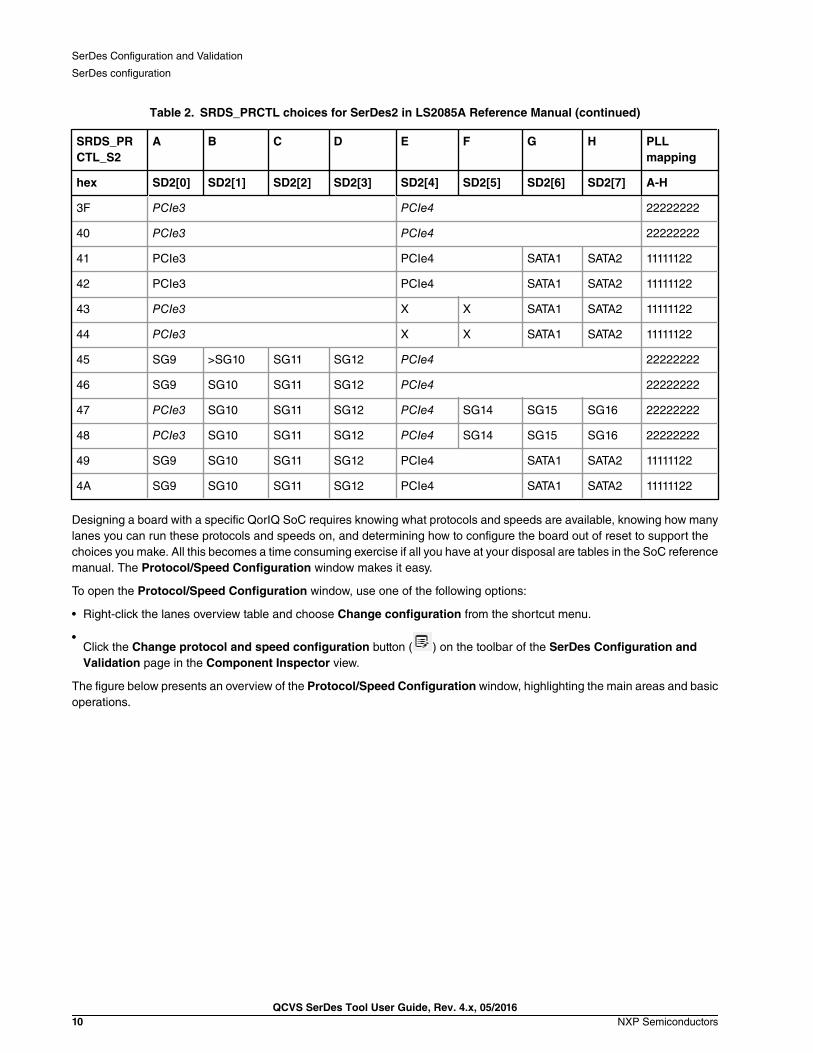
Table 2. SRDS_PRCTL choices for SerDes2 in LS2085A Reference Manual (continued)
SRDS_PRCTL_S2
A B C D E F G H PLLmapping
hex SD2[0] SD2[1] SD2[2] SD2[3] SD2[4] SD2[5] SD2[6] SD2[7] A-H
3F PCIe3 PCIe4 22222222
40 PCIe3 PCIe4 22222222
41 PCIe3 PCIe4 SATA1 SATA2 11111122
42 PCIe3 PCIe4 SATA1 SATA2 11111122
43 PCIe3 X X SATA1 SATA2 11111122
44 PCIe3 X X SATA1 SATA2 11111122
45 SG9 >SG10 SG11 SG12 PCIe4 22222222
46 SG9 SG10 SG11 SG12 PCIe4 22222222
47 PCIe3 SG10 SG11 SG12 PCIe4 SG14 SG15 SG16 22222222
48 PCIe3 SG10 SG11 SG12 PCIe4 SG14 SG15 SG16 22222222
49 SG9 SG10 SG11 SG12 PCIe4 SATA1 SATA2 11111122
4A SG9 SG10 SG11 SG12 PCIe4 SATA1 SATA2 11111122
Designing a board with a specific QorIQ SoC requires knowing what protocols and speeds are available, knowing how manylanes you can run these protocols and speeds on, and determining how to configure the board out of reset to support thechoices you make. All this becomes a time consuming exercise if all you have at your disposal are tables in the SoC referencemanual. The Protocol/Speed Configuration window makes it easy.
To open the Protocol/Speed Configuration window, use one of the following options:
• Right-click the lanes overview table and choose Change configuration from the shortcut menu.
•Click the Change protocol and speed configuration button ( ) on the toolbar of the SerDes Configuration andValidation page in the Component Inspector view.
The figure below presents an overview of the Protocol/Speed Configuration window, highlighting the main areas and basicoperations.
SerDes Configuration and Validation
SerDes configuration
QCVS SerDes Tool User Guide, Rev. 4.x, 05/201610 NXP Semiconductors

Figure 7. Protocol/Speed Configuration window (overview)
The Protocol/Speed Configuration window allows you to choose the protocols and speeds you want in your design, andshows you only the table rows (that is, the SRDS_PRTCL_Sn choices) that are relevant. It spares you the clutter of dozensof irrelevant table options. This window can also be used to quickly determine if a particular combination of protocols andspeeds is supported.
The Protocol/Speed Configuration window can be divided into the following two panes:
• Criteria pane: The left portion of the window, the Criteria pane, is where you specify the protocols and speeds you areinterested in and how you would like those selections used for filtering. This pane has a collapsable tree that containsevery protocol/speed supported by all the SerDes modules on the SoC. Each protocol/speed has a checkbox. You canselect the protocols/speeds you are interested in. Above the tree is a selector that controls how the selected items willbe used to filter the SRDS_PRTCL_Sn options on the right:
• Compact AND. In this filtering mode, only SRDS_PRTCL_Sn options that collectively and simultaneously support allthe selected protocols/speeds are shown. If you have selected a combination of protocols/speeds that cannotsimultaneously be supported by the SoC, a message indicating this will be displayed in place of SRDS_PRTCL_Sntables. In addition, relevant SRDS_PRTCL_Sn choices that differ only in lanes containing protocols/speeds that arenot selected will be combined, producing a more compact set of results. For example, if SRDS_PRTCL_Sn options 1and 2 both have the desired PCIe Gen 2 protocol and speed in lanes 0-3, but one option has Aurora in lanes 4-7 andthe other option has SATA in those lanes, this filtering mode will show only option 1 and display lanes 4-7 as unnameddark-grey cells. The idea here is that because you expressed no interest in either Aurora or SATA, both options 1 and2 equally meet your needs. This filtering mode therefore provides the most concise results.
• Expanded AND. This filtering mode is similar to Compact AND except that it does not combine equivalent choices toreduce the result set. In the example above for Compact AND, both options 1 and 2 will be shown in the results. Thenon-relevant lanes (4-7) will be displayed in named dark-grey cells; therefore, allowing you to see the protocol/speedfor these lanes.
• Expanded OR. This filtering mode shows all the SRDS_PRTCL_Sn options that contain any of the selected protocols/speeds, whether or not the protocols/speeds you selected can all be supported simultaneously. For example, if youselect every protocol/speed and choose Expanded OR, the results area will show every SRDS_PRTCL_Sn option theSoC makes available. However, of course, the SoC cannot support every protocol/speed simultaneously; the ANDmodes would show an empty result set in this situation. The OR mode is more suited for browsing than decisionmaking.
• Results pane: The right portion of the window, the Results pane, shows you the SRDS_PRTCL_Sn options that meetthe criteria on the left. This pane has the subset of the SRDS_PRTCL_Sn options that meet the criteria established onthe left. These options are displayed in tables, similar to how they are presented in the SoC reference manual (see figurebelow).
SerDes Configuration and Validation
SerDes configuration
QCVS SerDes Tool User Guide, Rev. 4.x, 05/2016NXP Semiconductors 11
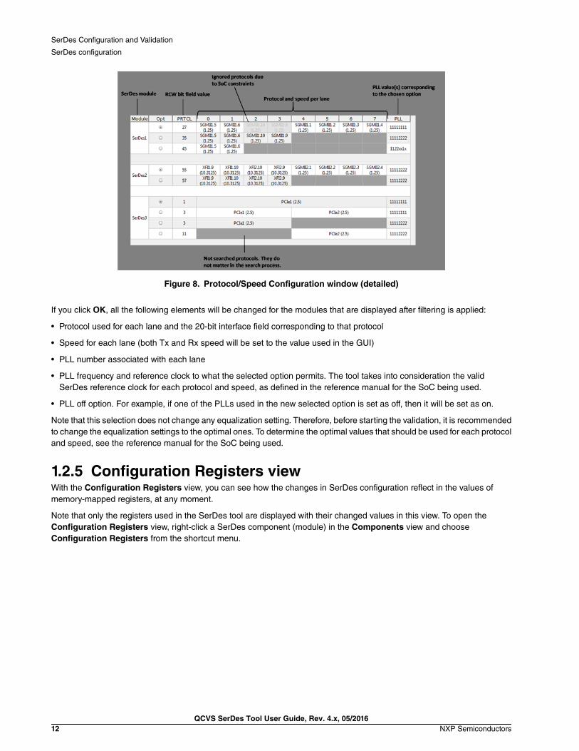
Figure 8. Protocol/Speed Configuration window (detailed)
If you click OK, all the following elements will be changed for the modules that are displayed after filtering is applied:
• Protocol used for each lane and the 20-bit interface field corresponding to that protocol
• Speed for each lane (both Tx and Rx speed will be set to the value used in the GUI)
• PLL number associated with each lane
• PLL frequency and reference clock to what the selected option permits. The tool takes into consideration the validSerDes reference clock for each protocol and speed, as defined in the reference manual for the SoC being used.
• PLL off option. For example, if one of the PLLs used in the new selected option is set as off, then it will be set as on.
Note that this selection does not change any equalization setting. Therefore, before starting the validation, it is recommendedto change the equalization settings to the optimal ones. To determine the optimal values that should be used for each protocoland speed, see the reference manual for the SoC being used.
1.2.5 Configuration Registers viewWith the Configuration Registers view, you can see how the changes in SerDes configuration reflect in the values ofmemory-mapped registers, at any moment.
Note that only the registers used in the SerDes tool are displayed with their changed values in this view. To open theConfiguration Registers view, right-click a SerDes component (module) in the Components view and chooseConfiguration Registers from the shortcut menu.
SerDes Configuration and Validation
SerDes configuration
QCVS SerDes Tool User Guide, Rev. 4.x, 05/201612 NXP Semiconductors

Figure 9. Configuration Registers view
1.2.6 Errata supportThe SerDes tool provides support for the errata that impact the SerDes IP block. By default, the SerDes tool supports thelatest approved and published errata at the time of the QCVS release.
The errata depend on the conditions that can be read from the target (such as, device type, selected protocol) and/orconditions that are external to the device or SerDes IP block (such as, outside temperature, settings in other IP blocks).
The SerDes tool addresses the errata in the following ways:
• If an erratum becomes applicable or may become applicable, then a warning message is displayed in the Problemsview that contains the description of the erratum as described in the errata document. The Problems view in the figurebelow shows descriptions of two such errata.
Figure 10. Errata displayed in Problems view
• Any erratum that becomes active due to a change made in the Protocol/Speed Configuration window is displayed asa message at the bottom of the window, besides displaying in the Problems view. The Protocol/Speed Configurationwindow in the figure below shows descriptions of two such errata.
SerDes Configuration and Validation
SerDes configuration
QCVS SerDes Tool User Guide, Rev. 4.x, 05/2016NXP Semiconductors 13

Figure 11. Errata displayed in Protocol/Speed Configuration window
• Any errata that depend on the conditions that cannot be determined by the SerDes tool are always displayed. Thismakes the user aware that such errata may become active, and the user can take appropriate actions (for example,implement errata workarounds), if needed.
See the errata document of the SoC for additional details on the displayed errata warning.
NOTE
Note that:
• The user is not prevented from running the SerDes validation scenarios even if there are active errata. The user isresponsible to implement the necessary errata workaround.
• Automatic errata workaround implementation and switching errata on and off are features considered for future QCVSreleases
1.3 SerDes validationThis section describes how to validate the configuration of the SerDes block.
After a SerDes configuration has been created in terms of protocol/speed, lane receive and transmit, and PLL allocation, thequestion is whether that configuration will perform reliably under the intended type of traffic. For that, the SerDes validationcapability comes into the picture.
The validation relies on SerDes hardware block built-in, programmable test capabilities that are used to verify the block underdifferent traffic conditions. The validation programs the built-in testing capabilities, and then runs a series of tests. The resultsof the tests are displayed in a format that enables you to make a decision on whether or not the SerDes configuration isreliable. If the answer is no, then you need to adjust the SerDes configuration and run the validation again, until the reliableSerDes configuration is determined.
The added value of validation feature is:
• Easy programmability of SerDes built-in test capabilities
• One click run of the validation test, which includes applying SerDes configuration to the target, programming the test block,and collecting and aggregating the results
• A quick synthesis of the test results in industry standard interpretations, such as data eye diagram or recovered data streamdiagram
SerDes Configuration and Validation
SerDes validation
QCVS SerDes Tool User Guide, Rev. 4.x, 05/201614 NXP Semiconductors
The validation feature requires a working target connection and a valid license. For license details, see Licensing on page24.
Note that when validation is run, the following changes are made:
• All the protocol control registers are cleared
• SerDes is put into the Test mode, and the current configuration is applied (changes are made only to the SerDes memory-mapped registers)
• All idle filters are cleared
• The lane, on which validation is run, is set as the first lane (this is required by the SerDes Test mode)
• Tx output pad control signal for common mode is set to 0 (External and External Loopback UI scenario settings)
This section contains the following subsections:
• SerDes Validation pane on page 15
• Data generation modes on page 15
• SerDes validation scenarios on page 17
• SerDes validation best practices on page 21
• Target connection settings on page 22
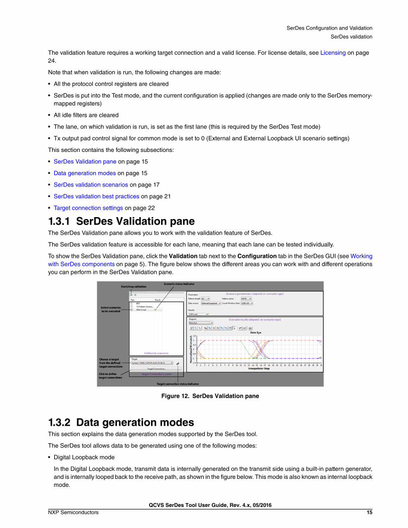
1.3.1 SerDes Validation paneThe SerDes Validation pane allows you to work with the validation feature of SerDes.
The SerDes validation feature is accessible for each lane, meaning that each lane can be tested individually.
To show the SerDes Validation pane, click the Validation tab next to the Configuration tab in the SerDes GUI (see Workingwith SerDes components on page 5). The figure below shows the different areas you can work with and different operationsyou can perform in the SerDes Validation pane.
Figure 12. SerDes Validation pane
1.3.2 Data generation modesThis section explains the data generation modes supported by the SerDes tool.
The SerDes tool allows data to be generated using one of the following modes:
• Digital Loopback mode
In the Digital Loopback mode, transmit data is internally generated on the transmit side using a built-in pattern generator,and is internally looped back to the receive path, as shown in the figure below. This mode is also known as internal loopbackmode.
SerDes Configuration and Validation
SerDes validation
QCVS SerDes Tool User Guide, Rev. 4.x, 05/2016NXP Semiconductors 15

Figure 13. Digital Loopback mode
• External Loopback mode
In the External Loopback mode, transmit data is internally generated on the transmit side using a built-in pattern generator,and is externally looped back to the receive path, as shown in the figure below. The user needs to provide an externalconnection between the SD_TX_P/SD_TX_N and SD_RX_P/SD_RX_N pins of the SerDes lane being validated.
Figure 14. External Loopback mode
• External mode
In the External mode, an external source, such as a link partner or an external test equipment, generates data that is inputto the receive path of the SerDes lane being validated. BIST and Jitter scope scenarios can be run in the External mode.When running BIST in the External mode, the selected test pattern must match the test pattern generated by the externalsource. When running the Jitter scope scenario in the External mode, the selected pattern length must match the externallysourced pattern.
SerDes Configuration and Validation
SerDes validation
QCVS SerDes Tool User Guide, Rev. 4.x, 05/201616 NXP Semiconductors

Figure 15. External mode
1.3.3 SerDes validation scenariosThe SerDes validation scenarios are mapped with the SerDes built-in test module, which can be programmed to performdifferent sets of tests.
Running a SerDes validation scenario involves the following steps:
1. Program the SerDes built-in test capability for a specific test. The scenario can be customized using the SerDesValidation pane (see SerDes Validation pane on page 15).
2. Set the mode in which the traffic is generated (Digital Loopback, External Loopback, or External (that is, traffic isgenerated from an SoC outside the source))
3. Set the SerDes self-test module into the Run mode, and process the traffic according to the user settings
4. Collect the results as the traffic is processed
5. After scenario completion, compile the results into a summary that can easily be interpreted by the user. Depending onthe complexity of the scenario and collected results, the summary can be in text format (BIST scenario) or as adiagram (Jitter scope scenario).
The SerDes tool provides you the following three validation scenarios to validate SerDes configuration:
• BIST scenario on page 17
• Tx pattern generation scenario on page 18
• Jitter scope scenario on page 19
1.3.3.1 BIST scenarioBuilt-in self-test (BIST) refers to a quick self-evaluation of a hardware block.
Running a BIST scenario involves the following steps:
1. Choose a pattern to be generated and how the traffic will flow through the lane (that is, data source mode: DigitalLoopback, External Loopback, or External).
2. Choose a count window that represents how much traffic will be generated and analyzed by the SerDes lane. It is set inbits and corresponds to a time value. The count window can widely vary from seconds to days, having direct impact onwhen the BIST results will be available.
3. The traffic formed out of the chosen pattern flows through the SerDes lane and results are collected. Optionally, asBIST runs with the largest count window, the user can insert some check errors. The BIST output should contain the
SerDes Configuration and Validation
SerDes validation
QCVS SerDes Tool User Guide, Rev. 4.x, 05/2016NXP Semiconductors 17

same number of generated errors as the number of errors inserted. That is a quick, on-the-fly method to detect if somebits were lost.
4. After BIST scenario completion, a text summary is displayed, as shown in the figure below.
Figure 16. BIST validation scenario
1.3.3.2 Tx pattern generation scenarioRunning the Tx pattern generation scenario drives the SerDes module to generate a specific pattern (set up by the user)on the Tx side of the lane that is being verified.
The Tx pattern generation scenario is not an actual validation scenario because no results are collected when it runs.
The figure below shows how the Tx pattern generation scenario works.
Figure 17. Tx pattern generation scenario
The Tx pattern generation scenario can be used in an environment with two devices connected such that:
• One device starts transmitting data with the Tx pattern generation scenario
• The other device verifies the received data with BIST or Jitter scope scenario in the External mode
• The Tx pattern generation scenario continues to run until the stop button is pressed
The figure below depicts the Tx pattern generation scenario use case described above.
SerDes Configuration and Validation
SerDes validation
QCVS SerDes Tool User Guide, Rev. 4.x, 05/201618 NXP Semiconductors

Figure 18. Tx pattern generation scenario use case
1.3.3.3 Jitter scope scenarioThe Jitter scope scenario displays the results of the SerDes configuration validation as a diagram (data eye diagram orrecovered data stream diagram).
With Jitter scope scenario, a pattern is repeatedly input into the receive path and a sampling point is moved across theincoming data stream, which gets compared to either 1 or 0. The bit is either 1 or 0 until it gets to the transition area. Withinthe transition area, the number of mismatches will be proportional to the bit error rate. The data eye diagram provides ameasurement of eye opening in the receive path. The recovered data stream diagram shows the received pattern.
In the Digital Loopback and External Loopback modes, the pattern is generated by the SerDes block. In case of the Externalmode, you can send any pattern from an external source (such as a test equipment), as long as it matches the selectedlength.
The figure below shows how the Jitter scope scenario works.
Figure 19. Jitter scope scenario
The figure below describes the data eye and recovered data stream diagrams.
SerDes Configuration and Validation
SerDes validation
QCVS SerDes Tool User Guide, Rev. 4.x, 05/2016NXP Semiconductors 19

Figure 20. Data eye and recovered data stream diagrams
The raw data based on which the Jitter scope diagrams are created can be retrieved from /<workspace_folder>/<project_name>/.SerDes_QorIQ_<id>_<device_name>/SerDes<module_index>_LN<lane_index>_JS_results.txt.
The text file contains input for the data eye and recovered data stream diagrams as comma-separated values.
Each line from the raw data contains three values:
• Step number: Represents how many times the bits in a count window are compared against an expected value. Thenumber of steps ensures that each bit is verified at least once.
• Number of mismatches: Indicates the sum of all the bits from a count window that do not match with a compare bit
• Normalized number of mismatches, that is, the number of mismatches scaled to the interval [-1, 1], where 1 indicates100% 1s and -1 indicates 100% 0s
You should expect a delay of certain amount of time before Jitter scope results (data eye and recovered data stream diagrams)are displayed. The delay depends on the selected pattern length and speed. The table below shows the approximate expecteddelays.
Table 3. Approximate expected delays
Pattern Length 1.25G 2.5G 3.125G
5G
6.25G
10.3125G
10-bits 6 min 3 min 1.5 min N/A
20-bits 14 min 7 min 3 min 1.5 min
40-bits 26 min 13 min 7 min 4 min
127-bits 84 min 42 min 21 min N/A
240-bits 168 min 84 min 42 min 21 min
254-bits N/A N/A N/A 21 min
511-bits 336 min 168 min 84 min N/A
1022-bits N/A N/A N/A 84 min
SerDes Configuration and Validation
SerDes validation
QCVS SerDes Tool User Guide, Rev. 4.x, 05/201620 NXP Semiconductors
1.3.4 SerDes validation best practicesThe purpose of a SerDes validation is to gradually refine a SerDes configuration, by checking it against the provided set ofscenarios.
Following are the best practice steps for running a SerDes validation:
1. Create a SerDes configuration by reading the configuration set on the target.
• For each lane, choose the desired set of protocols using the Protocol/Speed Configuration window.
• Use the protocol filter capability rather than seeking through the multitude of options.
• Change equalization settings for the desired lane. See the reference manual for the SoC being used, to know theoptimal values that should be used for each protocol and speed.
2. Check if the lane you want to verify is powered up; otherwise, power it up.
3. Ensure that the input reference clock from the target (for the module and PLL you are using) matches the one thatSerDes expects to receive (the one specified in the PLL configuration view).
4. Run the BIST scenario in the Digital Loopback mode with a small (few seconds) count window.
5. Run the BIST scenario again in the Digital Loopback mode with a larger count window. Use the largest count window toinsert errors and verify if they are received correctly.
6. Run the BIST scenario in the External Loopback mode with a sufficient count (for example, in minutes) window. Set upthe External Loopback mode according to the protocol you chose for that lane and the design of the target you areusing. For example, if you chose PCIe as the protocol, ensure that a PCIe loopback card is installed on the target, andit is connected to the corresponding module and lane you are trying to validate.
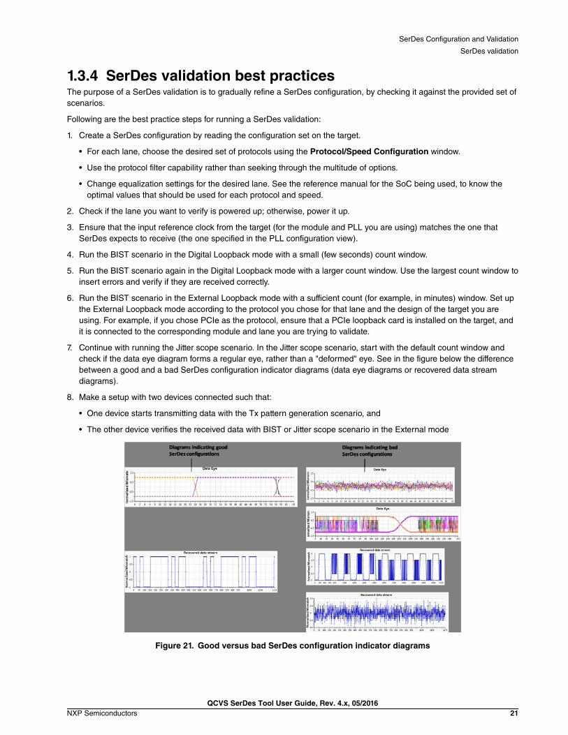
7. Continue with running the Jitter scope scenario. In the Jitter scope scenario, start with the default count window andcheck if the data eye diagram forms a regular eye, rather than a "deformed" eye. See in the figure below the differencebetween a good and a bad SerDes configuration indicator diagrams (data eye diagrams or recovered data streamdiagrams).
8. Make a setup with two devices connected such that:
• One device starts transmitting data with the Tx pattern generation scenario, and
• The other device verifies the received data with BIST or Jitter scope scenario in the External mode
Figure 21. Good versus bad SerDes configuration indicator diagrams
SerDes Configuration and Validation
SerDes validation
QCVS SerDes Tool User Guide, Rev. 4.x, 05/2016NXP Semiconductors 21

1.3.5 Target connection settingsThe Target connections window allows you to configure settings for your target connection.
The SerDes validation requires a working connection to a target. You can define multiple target connections, and then chooseone to work with.
The figure below shows how to open the Target connections window, and how to choose target connection settings fromthis window.
Figure 22. Target connections window
If the target connection is lost during validation, then the chain icon showing in the Target group will change to a brokenchain icon with an error icon. In that case, you would need to re-establish the connection by clicking again the Targetconnections button.
1.4 How to use a SerDes configurationThis section describes how to use a SerDes configuration to program the target.
Once an optimized SerDes configuration is determined, it can be used to program the target. The SerDes configurationconsists of:
• Values of SerDes memory-mapped registers. For details, see Code generation on page 23.
• RCW settings for the lanes protocols/speeds. For details, see Synchronization between SerDes and PBL on page 23.
Therefore, using a SerDes configuration means flashing a new RCW and then writing into memory-mapped registers.
This section contains the following subsections:
• RCW settings on page 23
• Code generation on page 23
• Synchronization between SerDes and PBL on page 23
SerDes Configuration and Validation
How to use a SerDes configuration
QCVS SerDes Tool User Guide, Rev. 4.x, 05/201622 NXP Semiconductors

1.4.1 RCW settingsThe RCW settings determine how a platform is configured, before any software runs on it.
The protocols/speeds allocated to each SerDes lane, the reference clock SerDes expects to receive for each PLL, and thePower-Down state for each PLL are usually set in RCW. See Synchronization between SerDes and PBL on page 23 fordetails on how to push all these changes into the corresponding RCW bits from PBL.
1.4.2 Code generationThe SerDes memory-mapped register values can be obtained by clicking the Generate Processor Expert Code buttonon the toolbar of the Components view.
The register values are generated in various code formats. Currently, the SerDes tool only supports U-Boot commands andC code as code formats. The figure below shows how to generate code.
Figure 23. Generating code
1.4.3 Synchronization between SerDes and PBLA pre-boot loader (PBL) is a binary image that is used to configure a hardware platform before any other software (forexample, U-Boot) can run on it.
The RCW used to initially set up the platform contains several bits related to SerDes configuration. A SerDes configurationcan be reflected into updated RCW bits with just one button click.
Before performing synchronization, you need to create a PBL component. After creating the PBL component, perform
synchronization between SerDes and PBL by clicking the Apply the configuration to PBL component button ( ) on thetoolbar of the SerDes Configuration and Validation page in the Component Inspector view, as shown in the figure below.When no PBL component exists in the project, the button is grayed out with tooltip text as "You must have a PBL componentin your project in order to apply the serdes configuration also into RCW."
SerDes Configuration and Validation
How to use a SerDes configuration
QCVS SerDes Tool User Guide, Rev. 4.x, 05/2016NXP Semiconductors 23
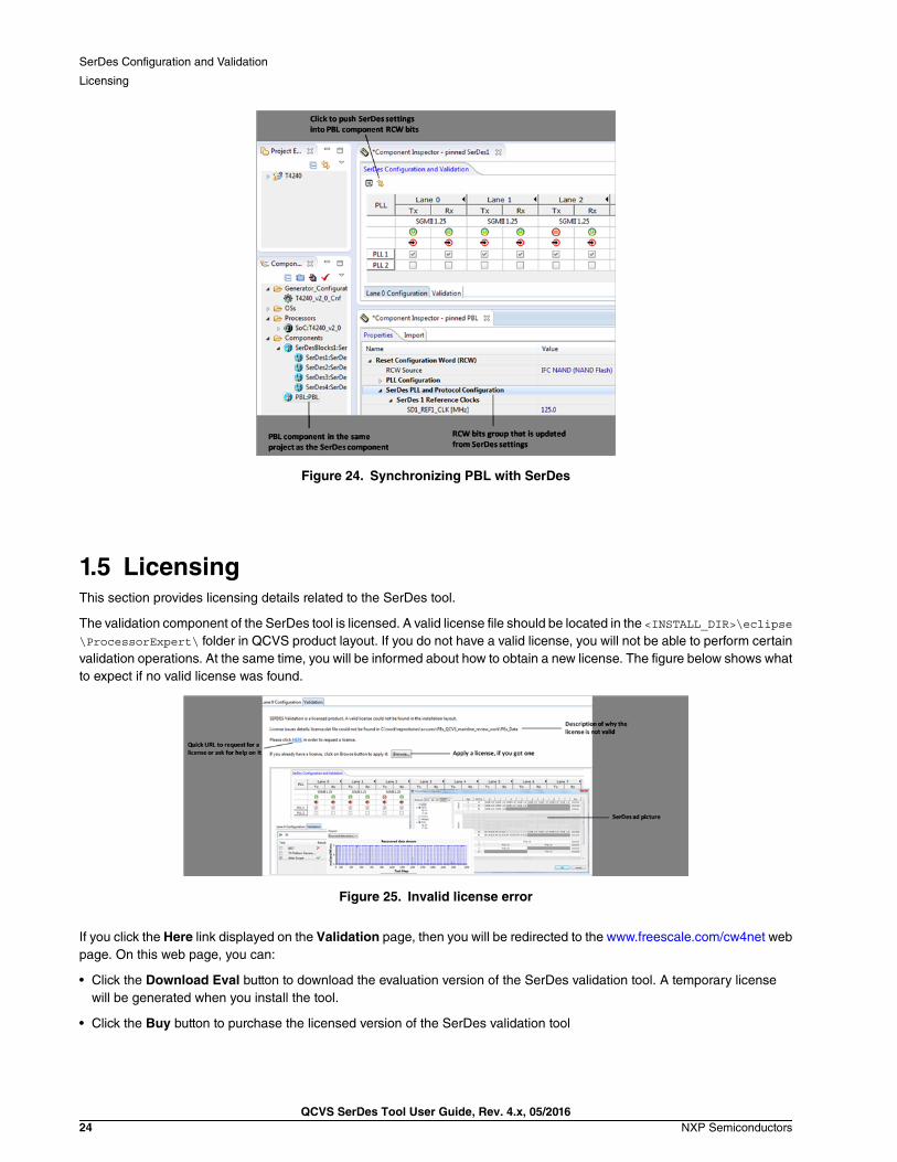
Figure 24. Synchronizing PBL with SerDes
1.5 LicensingThis section provides licensing details related to the SerDes tool.
The validation component of the SerDes tool is licensed. A valid license file should be located in the <INSTALL_DIR>\eclipse\ProcessorExpert\ folder in QCVS product layout. If you do not have a valid license, you will not be able to perform certainvalidation operations. At the same time, you will be informed about how to obtain a new license. The figure below shows whatto expect if no valid license was found.
Figure 25. Invalid license error
If you click the Here link displayed on the Validation page, then you will be redirected to the www.freescale.com/cw4net webpage. On this web page, you can:
• Click the Download Eval button to download the evaluation version of the SerDes validation tool. A temporary licensewill be generated when you install the tool.
• Click the Buy button to purchase the licensed version of the SerDes validation tool
SerDes Configuration and Validation
Licensing
QCVS SerDes Tool User Guide, Rev. 4.x, 05/201624 NXP Semiconductors

Index
A
Acronyms 3
B
BIST scenario 17
C
Code generation 23Configuration registers view 12Creating a SerDes project 4
D
Data generation modes 15
E
Errata support 13
J
Jitter scope scenario 19
L
Lane Configuration pane 7
M
Module Overview pane 7
P
PLL Configuration pane 8Protocol/Speed Configuration window 9
R
RCW settings 23
S
SerDes hardware block challenges 4SerDes validation best practices 21SerDes Validation pane 15SerDes validation scenarios 17Synchronization between SerDes and PBL 23
T
Target connection settings 22Tx pattern generation scenario 18
W
Working with SerDes components 5
Index
QCVS SerDes Tool User Guide, Rev. 4.x, 05/2016NXP Semiconductors 25

How To Reach Us
Home Page:
nxp.com
Web Support:
nxp.com/support
Information in this document is provided solely to enable system and software implementers
to use Freescale products. There are no express or implied copyright licenses granted
hereunder to design or fabricate any integrated circuits based on the information in this
document. Freescale reserves the right to make changes without further notice to any
products herein.
Freescale makes no warranty, representation, or guarantee regarding the suitability of its
products for any particular purpose, nor does Freescale assume any liability arising out of the
application or use of any product or circuit, and specifically disclaims any and all liability,
including without limitation consequential or incidental damages. “Typical” parameters that
may be provided in Freescale data sheets and/or specifications can and do vary in different
applications, and actual performance may vary over time. All operating parameters, including
“typicals,” must be validated for each customer application by customer's technical experts.
Freescale does not convey any license under its patent rights nor the rights of others.
Freescale sells products pursuant to standard terms and conditions of sale, which can be
found at the following address: nxp.com/SalesTermsandConditions.
Freescale, the Freescale logo, CodeWarrior, QorIQ, and Processor Expert are trademarks of
Freescale Semiconductor, Inc., Reg. U.S. Pat. & Tm. Off. All other product or service names
are the property of their respective owners.
Ⓒ 2016 Freescale Semiconductor, Inc.
QCVS_SerDes_User_GuideRev. 4.x05/2016


