605
External Memory InterfaceHandbook Volume 2: DesignGuidelines
Updated for Intel® Quartus® Prime Design Suite: 17.0
SubscribeSend Feedback
EMI_DG | 2017.05.08Latest document on the web: PDF | HTML
Contents
1. Planning Pin and FPGA Resources...................................................................................91.1. Interface Pins........................................................................................................9
1.1.1. Estimating Pin Requirements..................................................................... 121.1.2. DDR, DDR2, DDR3, and DDR4 SDRAM Clock Signals....................................131.1.3. DDR, DDR2, DDR3, and DDR4 SDRAM Command and Address Signals........... 131.1.4. DDR, DDR2, DDR3, and DDR4 SDRAM Data, Data Strobes, DM/DBI, and
Optional ECC Signals................................................................................ 141.1.5. DDR, DDR2, DDR3, and DDR4 SDRAM DIMM Options...................................151.1.6. QDR II, QDR II+, and QDR II+ Xtreme SRAM Clock Signals..........................181.1.7. QDR II, QDR II+ and QDR II+ Xtreme SRAM Command Signals.................... 191.1.8. QDR II, QDR II+ and QDR II+ Xtreme SRAM Address Signals....................... 191.1.9. QDR II, QDR II+ and QDR II+ Xtreme SRAM Data, BWS, and QVLD Signals....201.1.10. QDR IV SRAM Clock Signals.....................................................................201.1.11. QDR IV SRAM Commands and Addresses, AP, and AINV Signals....................211.1.12. QDR IV SRAM Data, DINV, and QVLD Signals............................................. 221.1.13. RLDRAM II and RLDRAM 3 Clock Signals...................................................231.1.14. RLDRAM II and RLDRAM 3 Commands and Addresses................................ 241.1.15. RLDRAM II and RLDRAM 3 Data, DM and QVLD Signals.............................. 241.1.16. LPDDR2 and LPDDR3 Clock Signal........................................................... 251.1.17. LPDDR2 and LPDDR3 Command and Address Signal...................................261.1.18. LPDDR2 and LPDDR3 Data, Data Strobe, and DM Signals............................261.1.19. Maximum Number of Interfaces............................................................... 261.1.20. OCT Support .........................................................................................37
1.2. Guidelines for Intel Arria® 10 External Memory Interface IP.......................................381.2.1. General Pin-Out Guidelines for Arria 10 EMIF IP........................................... 381.2.2. Resource Sharing Guidelines for Arria 10 EMIF IP......................................... 43
1.3. Guidelines for Intel Stratix® 10 External Memory Interface IP.................................... 451.3.1. General Pin-Out Guidelines for Stratix 10 EMIF IP.........................................451.3.2. Resource Sharing Guidelines for Stratix 10 EMIF IP.......................................50
1.4. Guidelines for UniPHY-based External Memory Interface IP........................................ 511.4.1. General Pin-out Guidelines for UniPHY-based External Memory Interface IP......511.4.2. Pin-out Rule Exceptions for ×36 Emulated QDR II and QDR II+ SRAM
Interfaces in Arria II, Stratix III and Stratix IV Devices................................. 531.4.3. Pin-out Rule Exceptions for RLDRAM II and RLDRAM 3 Interfaces................... 581.4.4. Pin-out Rule Exceptions for QDR II and QDR II+ SRAM Burst-length-of-two
Interfaces............................................................................................... 601.4.5. Pin Connection Guidelines Tables................................................................611.4.6. PLLs and Clock Networks.......................................................................... 71
1.5. Using PLL Guidelines............................................................................................ 751.6. PLL Cascading..................................................................................................... 761.7. DLL....................................................................................................................761.8. Other FPGA Resources..........................................................................................781.9. Document Revision History....................................................................................78
2. DDR2, DDR3, and DDR4 SDRAM Board Design Guidelines............................................. 812.1. Leveling and Dynamic Termination......................................................................... 82
2.1.1. Read and Write Leveling........................................................................... 822.1.2. Dynamic ODT.......................................................................................... 84
Contents
External Memory Interface Handbook Volume 2: Design Guidelines Send Feedback
2
2.1.3. Dynamic On-Chip Termination................................................................... 842.1.4. Dynamic On-Chip Termination in Stratix III and Stratix IV Devices..................852.1.5. Dynamic OCT in Stratix V Devices.............................................................. 872.1.6. Dynamic On-Chip Termination (OCT) in Arria 10 and Stratix 10 Devices.......... 87
2.2. DDR2 Terminations and Guidelines......................................................................... 872.2.1. Termination for DDR2 SDRAM.................................................................... 872.2.2. DDR2 Design Layout Guidelines................................................................. 932.2.3. General Layout Guidelines.........................................................................932.2.4. Layout Guidelines for DDR2 SDRAM Interface.............................................. 94
2.3. DDR3 Terminations in Arria V, Cyclone V, Stratix III, Stratix IV, and Stratix V.............. 972.3.1. Terminations for Single-Rank DDR3 SDRAM Unbuffered DIMM........................982.3.2. Terminations for Multi-Rank DDR3 SDRAM Unbuffered DIMM..........................992.3.3. Terminations for DDR3 SDRAM Registered DIMM........................................ 1002.3.4. Terminations for DDR3 SDRAM Load-Reduced DIMM.................................. 1002.3.5. Terminations for DDR3 SDRAM Components With Leveling.......................... 101
2.4. DDR3 and DDR4 on Arria 10 and Stratix 10 Devices................................................1012.4.1. Dynamic On-Chip Termination (OCT) in Arria 10 and Stratix 10 Devices.........1012.4.2. Dynamic On-Die Termination (ODT) in DDR4..............................................1022.4.3. Choosing Terminations on Arria 10 Devices................................................1022.4.4. On-Chip Termination Recommendations for DDR3 and DDR4 on Arria 10
Devices.................................................................................................1022.5. Layout Approach................................................................................................1032.6. Channel Signal Integrity Measurement..................................................................104
2.6.1. Importance of Accurate Channel Signal Integrity Information....................... 1042.6.2. Understanding Channel Signal Integrity Measurement.................................1042.6.3. How to Enter Calculated Channel Signal Integrity Values............................. 1052.6.4. Guidelines for Calculating DDR3 Channel Signal Integrity.............................1062.6.5. Guidelines for Calculating DDR4 Channel Signal Integrity.............................108
2.7. Design Layout Guidelines.................................................................................... 1112.7.1. General Layout Guidelines....................................................................... 1122.7.2. Layout Guidelines for DDR3 and DDR4 SDRAM Interfaces............................ 1132.7.3. Length Matching Rules............................................................................ 1162.7.4. Spacing Guidelines................................................................................. 1172.7.5. Layout Guidelines for DDR3 and DDR4 SDRAM Wide Interface (>72 bits).......118
2.8. Package Deskew................................................................................................ 1212.8.1. Package Deskew Recommendation for Stratix V Devices.............................. 1212.8.2. DQ/DQS/DM Deskew.............................................................................. 1222.8.3. Address and Command Deskew................................................................1222.8.4. Package Deskew Recommendations for Arria 10 and Stratix 10 Devices.........1222.8.5. Deskew Example....................................................................................1232.8.6. Package Migration.................................................................................. 1242.8.7. Package Deskew for RLDRAM II and RLDRAM 3.......................................... 125
2.9. Document Revision History..................................................................................125
3. Dual-DIMM DDR2 and DDR3 SDRAM Board Design Guidelines.....................................1283.1. General Layout Guidelines................................................................................... 1283.2. Dual-Slot Unbuffered DDR2 SDRAM...................................................................... 129
3.2.1. Overview of ODT Control.........................................................................1303.2.2. DIMM Configuration................................................................................1313.2.3. Dual-DIMM Memory Interface with Slot 1 Populated....................................1323.2.4. Dual-DIMM with Slot 2 Populated............................................................. 133
Contents
Send Feedback External Memory Interface Handbook Volume 2: Design Guidelines
3
3.2.5. Dual-DIMM Memory Interface with Both Slot 1 and Slot 2 Populated............. 1343.2.6. Dual-DIMM DDR2 Clock, Address, and Command Termination and Topology... 1373.2.7. Control Group Signals.............................................................................1383.2.8. Clock Group Signals................................................................................138
3.3. Dual-Slot Unbuffered DDR3 SDRAM..................................................................... 1383.3.1. Comparison of DDR3 and DDR2 DQ and DQS ODT Features and Topology...... 1393.3.2. Dual-DIMM DDR3 Clock, Address, and Command Termination and Topology... 1393.3.3. FPGA OCT Features................................................................................ 140
3.4. Document Revision History..................................................................................141
4. LPDDR2 and LPDDR3 SDRAM Board Design Guidelines............................................... 1424.1. LPDDR2 Guidance.............................................................................................. 142
4.1.1. LPDDR2 SDRAM Configurations................................................................ 1424.1.2. OCT Signal Terminations for Arria V and Cyclone V Devices..........................1454.1.3. General Layout Guidelines....................................................................... 1484.1.4. LPDDR2 Layout Guidelines.......................................................................148
4.2. LPDDR3 Guidance.............................................................................................. 1504.2.1. Signal Integrity, Board Skew, and Board Setting Parameters........................ 1514.2.2. LPDDR3 Layout Guidelines.......................................................................1514.2.3. Package Deskew.................................................................................... 151
4.3. Document Revision History..................................................................................155
5. RLDRAM II and RLDRAM 3 Board Design Guidelines................................................... 1565.1. RLDRAM II Configurations................................................................................... 1575.2. RLDRAM 3 Configurations....................................................................................1585.3. Signal Terminations............................................................................................ 160
5.3.1. Input to the FPGA from the RLDRAM Components.......................................1625.3.2. Outputs from the FPGA to the RLDRAM II and RLDRAM 3 Components.......... 1625.3.3. RLDRAM II Termination Schemes..............................................................1635.3.4. RLDRAM 3 Termination Schemes.............................................................. 163
5.4. PCB Layout Guidelines........................................................................................ 1645.5. General Layout Guidelines................................................................................... 1655.6. RLDRAM II and RLDRAM 3 Layout Guidelines......................................................... 1655.7. Layout Approach................................................................................................167
5.7.1. Arria V and Stratix V Board Setting Parameters.......................................... 1685.7.2. Arria 10 Board Setting Parameters............................................................168
5.8. Package Deskew for RLDRAM II and RLDRAM 3...................................................... 1685.9. Document Revision History..................................................................................169
6. QDR II and QDR-IV SRAM Board Design Guidelines.................................................... 1706.1. QDR II SRAM Configurations................................................................................1716.2. Signal Terminations............................................................................................ 172
6.2.1. Output from the FPGA to the QDR II SRAM Component............................... 1746.2.2. Input to the FPGA from the QDR II SRAM Component................................. 1746.2.3. Termination Schemes..............................................................................174
6.3. General Layout Guidelines................................................................................... 1766.4. QDR II Layout Guidelines.................................................................................... 1776.5. QDR II SRAM Layout Approach.............................................................................1786.6. Package Deskew for QDR II and QDR-IV................................................................1806.7. QDR-IV Layout Approach.....................................................................................1806.8. QDR-IV Layout Guidelines................................................................................... 1816.9. Document Revision History..................................................................................182
Contents
External Memory Interface Handbook Volume 2: Design Guidelines Send Feedback
4
7. Implementing and Parameterizing Memory IP............................................................1847.1. Installing and Licensing IP Cores.......................................................................... 1847.2. Design Flow.......................................................................................................185
7.2.1. IP Catalog Design Flow........................................................................... 1867.2.2. Qsys System Integration Tool Design Flow................................................. 193
7.3. UniPHY-Based External Memory Interface IP.......................................................... 1957.3.1. Qsys Interfaces......................................................................................1967.3.2. Generated Files for Memory Controllers with the UniPHY IP.......................... 2157.3.3. Parameterizing Memory Controllers...........................................................2187.3.4. Board Settings ......................................................................................2327.3.5. Controller Settings for UniPHY IP..............................................................2437.3.6. Diagnostics for UniPHY IP........................................................................ 247
7.4. Intel Arria 10 External Memory Interface IP........................................................... 2487.4.1. Qsys Interfaces......................................................................................2487.4.2. Generated Files for Arria 10 External Memory Interface IP........................... 2607.4.3. Arria 10 EMIF IP DDR4 Parameters........................................................... 2647.4.4. Arria 10 EMIF IP DDR3 Parameters........................................................... 2867.4.5. Arria 10 EMIF IP LPDDR3 Parameters........................................................3057.4.6. Arria 10 EMIF IP QDR-IV Parameters.........................................................3207.4.7. Arria 10 EMIF IP QDR II/II+/II+ Xtreme Parameters...................................3327.4.8. Arria 10 EMIF IP RLDRAM 3 Parameters.....................................................3437.4.9. Equations for Arria 10 EMIF IP Board Skew Parameters............................... 355
7.5. Intel Stratix 10 External Memory Interface IP........................................................ 3617.5.1. Qsys Interfaces......................................................................................3617.5.2. Generated Files for Stratix 10 External Memory Interface IP.........................3727.5.3. Stratix 10 EMIF IP DDR4 Parameters.........................................................3777.5.4. Stratix 10 EMIF IP DDR3 Parameters.........................................................3977.5.5. Stratix 10 EMIF IP LPDDR3 Parameters..................................................... 4137.5.6. Stratix 10 EMIF IP QDR-IV Parameters...................................................... 4287.5.7. Stratix 10 EMIF IP QDR II/II+/II+ Xtreme Parameters................................ 4407.5.8. Stratix 10 EMIF IP RLDRAM 3 Parameters.................................................. 451
7.6. Document Revision History..................................................................................463
8. Simulating Memory IP.................................................................................................4688.1. Simulation Options.............................................................................................4688.2. Simulation Walkthrough with UniPHY IP.................................................................470
8.2.1. Simulation Scripts.................................................................................. 4718.2.2. Preparing the Vendor Memory Model.........................................................4718.2.3. Functional Simulation with Verilog HDL......................................................4748.2.4. Functional Simulation with VHDL.............................................................. 4748.2.5. Simulating the Example Design................................................................4758.2.6. UniPHY Abstract PHY Simulation...............................................................4768.2.7. PHY-Only Simulation...............................................................................4788.2.8. Post-fit Functional Simulation...................................................................4798.2.9. Simulation Issues...................................................................................481
8.3. Simulation Walkthrough with Arria 10 EMIF IP........................................................4838.3.1. Skip Calibration Versus Full Calibration......................................................4838.3.2. Arria 10 Abstract PHY Simulation..............................................................4848.3.3. Simulation Scripts.................................................................................. 4858.3.4. Functional Simulation with Verilog HDL......................................................485
Contents
Send Feedback External Memory Interface Handbook Volume 2: Design Guidelines
5
8.3.5. Functional Simulation with VHDL.............................................................. 4868.3.6. Simulating the Example Design................................................................487
8.4. Simulation Walkthrough with Stratix 10 EMIF IP..................................................... 4888.4.1. Skip Calibration Versus Full Calibration......................................................4898.4.2. Simulation Scripts.................................................................................. 4908.4.3. Functional Simulation with Verilog HDL......................................................4908.4.4. Functional Simulation with VHDL.............................................................. 4918.4.5. Simulating the Example Design................................................................491
8.5. Document Revision History..................................................................................493
9. Analyzing Timing of Memory IP.................................................................................. 4949.1. Memory Interface Timing Components.................................................................. 495
9.1.1. Source-Synchronous Paths...................................................................... 4959.1.2. Calibrated Paths.....................................................................................4959.1.3. Internal FPGA Timing Paths..................................................................... 4969.1.4. Other FPGA Timing Parameters................................................................ 496
9.2. FPGA Timing Paths............................................................................................. 4979.2.1. Arria II Device PHY Timing Paths.............................................................. 4979.2.2. Stratix III and Stratix IV PHY Timing Paths................................................ 4999.2.3. Arria V, Arria V GZ, Arria 10, Cyclone V, and Stratix V Timing paths...............501
9.3. Timing Constraint and Report Files for UniPHY IP....................................................5039.4. Timing Constraint and Report Files for Arria 10 EMIF IP........................................... 5059.5. Timing Constraint and Report Files for Stratix 10 EMIF IP........................................ 5069.6. Timing Analysis Description ................................................................................ 508
9.6.1. UniPHY IP Timing Analysis....................................................................... 5099.6.2. Timing Analysis Description for Arria 10 EMIF IP.........................................5179.6.3. Timing Analysis Description for Stratix 10 EMIF IP...................................... 521
9.7. Timing Report DDR.............................................................................................5249.8. Report SDC....................................................................................................... 5279.9. Calibration Effect in Timing Analysis......................................................................528
9.9.1. Calibration Emulation for Calibrated Path...................................................5289.9.2. Calibration Error or Quantization Error...................................................... 5289.9.3. Calibration Uncertainties......................................................................... 5299.9.4. Memory Calibration................................................................................ 529
9.10. Timing Model Assumptions and Design Rules........................................................5299.10.1. Memory Clock Output Assumptions......................................................... 5309.10.2. Write Data Assumptions........................................................................ 5319.10.3. Read Data Assumptions.........................................................................5339.10.4. DLL Assumptions..................................................................................5349.10.5. PLL and Clock Network Assumptions for Stratix III Devices........................ 534
9.11. Common Timing Closure Issues..........................................................................5359.11.1. Missing Timing Margin Report.................................................................5359.11.2. Incomplete Timing Margin Report........................................................... 5359.11.3. Read Capture Timing............................................................................ 5369.11.4. Write Timing........................................................................................5369.11.5. Address and Command Timing............................................................... 5369.11.6. PHY Reset Recovery and Removal........................................................... 5379.11.7. Clock-to-Strobe (for DDR and DDR2 SDRAM Only).................................... 5379.11.8. Read Resynchronization and Write Leveling Timing (for SDRAM Only).......... 537
9.12. Optimizing Timing............................................................................................ 538
Contents
External Memory Interface Handbook Volume 2: Design Guidelines Send Feedback
6
9.13. Timing Deration Methodology for Multiple Chip Select DDR2 and DDR3 SDRAMDesigns..........................................................................................................5399.13.1. Multiple Chip Select Configuration Effects.................................................5409.13.2. Timing Deration using the Board Settings................................................ 542
9.14. Early I/O Timing Estimation for Arria 10 EMIF IP...................................................5459.14.1. Performing Early I/O Timing Analysis for Arria 10 EMIF IP.......................... 546
9.15. Early I/O Timing Estimation for Stratix 10 EMIF IP................................................ 5479.15.1. Performing Early I/O Timing Analysis for Stratix 10 EMIF IP....................... 547
9.16. Performing I/O Timing Analysis.......................................................................... 5489.16.1. Performing I/O Timing Analysis with Third-Party Simulation Tools................5499.16.2. Performing Advanced I/O Timing Analysis with Board Trace Delay Model...... 549
9.17. Document Revision History................................................................................ 550
10. Debugging Memory IP...............................................................................................55110.1. Resource and Planning Issues............................................................................ 551
10.1.1. Dedicated IOE DQS Group Resources and Pins..........................................55110.1.2. Dedicated DLL Resources.......................................................................55210.1.3. Specific PLL Resources.......................................................................... 55310.1.4. Specific Global, Regional and Dual-Regional Clock Net Resources................ 55310.1.5. Planning Your Design............................................................................ 55310.1.6. Optimizing Design Utilization..................................................................554
10.2. Interface Configuration Performance Issues......................................................... 55410.2.1. Interface Configuration Bottleneck and Efficiency Issues............................ 555
10.3. Functional Issue Evaluation................................................................................55610.3.1. Correct Combination of the Quartus Prime Software and ModelSim - Intel
FPGA Edition Device Models.....................................................................55610.3.2. Intel IP Memory Model.......................................................................... 55710.3.3. Vendor Memory Model...........................................................................55710.3.4. Insufficient Memory in Your PC...............................................................55710.3.5. Transcript Window Messages..................................................................55810.3.6. Passing Simulation................................................................................55910.3.7. Modifying the Example Driver to Replicate the Failure................................559
10.4. Timing Issue Characteristics.............................................................................. 56010.4.1. Evaluating FPGA Timing Issues...............................................................56110.4.2. Evaluating External Memory Interface Timing Issues................................ 562
10.5. Verifying Memory IP Using the Signal Tap II Logic Analyzer.................................... 56210.5.1. Signals to Monitor with the Signal Tap II Logic Analyzer.............................564
10.6. Hardware Debugging Guidelines......................................................................... 56510.6.1. Create a Simplified Design that Demonstrates the Same Issue................... 56510.6.2. Measure Power Distribution Network....................................................... 56510.6.3. Measure Signal Integrity and Setup and Hold Margin.................................56510.6.4. Vary Voltage........................................................................................ 56610.6.5. Use Freezer Spray and Heat Gun............................................................ 56610.6.6. Operate at a Lower Speed..................................................................... 56610.6.7. Determine Whether the Issue Exists in Previous Versions of Software.......... 56610.6.8. Determine Whether the Issue Exists in the Current Version of Software....... 56610.6.9. Try A Different PCB...............................................................................56710.6.10. Try Other Configurations......................................................................56710.6.11. Debugging Checklist............................................................................568
10.7. Catagorizing Hardware Issues............................................................................ 56810.7.1. Signal Integrity Issues.......................................................................... 569
Contents
Send Feedback External Memory Interface Handbook Volume 2: Design Guidelines
7
10.7.2. Hardware and Calibration Issues.............................................................57110.8. EMIF Debug Toolkit Overview............................................................................. 57510.9. Document Revision History................................................................................ 575
11. Optimizing the Controller..........................................................................................57711.1. Factors Affecting Efficiency................................................................................ 577
11.1.1. Interface Standard............................................................................... 57811.1.2. Bank Management Efficiency..................................................................57811.1.3. Data Transfer.......................................................................................580
11.2. Ways to Improve Efficiency................................................................................58111.2.1. DDR2 SDRAM Controller........................................................................ 58211.2.2. Auto-Precharge Commands....................................................................58211.2.3. Additive Latency...................................................................................58411.2.4. Bank Interleaving................................................................................. 58511.2.5. Command Queue Look-Ahead Depth....................................................... 58711.2.6. Additive Latency and Bank Interleaving................................................... 58811.2.7. User-Controlled Refresh........................................................................ 58911.2.8. Frequency of Operation......................................................................... 59011.2.9. Burst Length........................................................................................59111.2.10. Series of Reads or Writes.....................................................................59111.2.11. Data Reordering................................................................................. 59111.2.12. Starvation Control...............................................................................59211.2.13. Command Reordering..........................................................................59311.2.14. Bandwidth......................................................................................... 59411.2.15. Efficiency Monitor............................................................................... 595
11.3. Document Revision History................................................................................ 596
12. PHY Considerations...................................................................................................59812.1. Core Logic and User Interface Data Rate..............................................................59812.2. Hard and Soft Memory PHY................................................................................59912.3. Sequencer.......................................................................................................59912.4. PLL, DLL and OCT Resource Sharing....................................................................60012.5. Pin Placement Consideration.............................................................................. 60112.6. Document Revision History................................................................................ 602
13. Power Estimation Methods for External Memory Interfaces......................................60313.1. Performing Vector-Based Power Analysis with the Power Analyzer........................... 60413.2. Document Revision History................................................................................ 604
Contents
External Memory Interface Handbook Volume 2: Design Guidelines Send Feedback
8
1. Planning Pin and FPGA ResourcesThis information is for board designers who must determine FPGA pin usage, to createboard layouts. The board design process sometimes occurs concurrently with the RTLdesign process.
Use this document with the External Memory Interfaces chapter of the relevant devicefamily handbook.
Typically, all external memory interfaces require the following FPGA resources:
• Interface pins
• PLL and clock network
• DLL
• Other FPGA resources—for example, core fabric logic, and on-chip termination(OCT) calibration blocks
After you know the requirements for your external memory interface, you can startplanning your system. The I/O pins and internal memory cannot be shared for otherapplications or external memory interfaces. However, if you do not have enough PLLs,DLLs, or clock networks for your application, you may share these resources amongmultiple external memory interfaces or modules in your system.
Ideally, any interface should reside entirely in a single bank; however, interfaces thatspan multiple adjacent banks or the entire side of a device are also fully supported. Inaddition, you may also have wraparound memory interfaces, where the design usestwo adjacent sides of the device and the memory interface logic resides in a devicequadrant. In some cases, top or bottom bank interfaces have higher supported clockrates than left or right or wraparound interfaces.
1.1. Interface Pins
Any I/O banks that do not support transceiver operations in Arria® II, Arria V, Arria10, Stratix® III, Stratix IV, and Stratix V devices support external memory interfaces.However, DQS (data strobe or data clock) and DQ (data) pins are listed in the devicepin tables and fixed at specific locations in the device. You must adhere to these pinlocations as these locations are optimized in routing to minimize skew and maximizemargin. Always check the external memory interfaces chapters from the devicehandbooks for the number of DQS and DQ groups supported in a particular device andthe pin table for the actual locations of the DQS and DQ pins.
The following table lists a summary of the number of pins required for variousexample memory interfaces. This table uses series OCT with calibration and parallelOCT with calibration, or dynamic calibrated OCT, when applicable, shown by the usageof RUP and RDN pins or RZQ pin.
EMI_DG | 2017.05.08
Send Feedback
Intel Corporation. All rights reserved. Intel, the Intel logo, Altera, Arria, Cyclone, Enpirion, MAX, Nios, Quartusand Stratix words and logos are trademarks of Intel Corporation or its subsidiaries in the U.S. and/or othercountries. Intel warrants performance of its FPGA and semiconductor products to current specifications inaccordance with Intel's standard warranty, but reserves the right to make changes to any products and servicesat any time without notice. Intel assumes no responsibility or liability arising out of the application or use of anyinformation, product, or service described herein except as expressly agreed to in writing by Intel. Intelcustomers are advised to obtain the latest version of device specifications before relying on any publishedinformation and before placing orders for products or services.*Other names and brands may be claimed as the property of others.
ISO9001:2015Registered
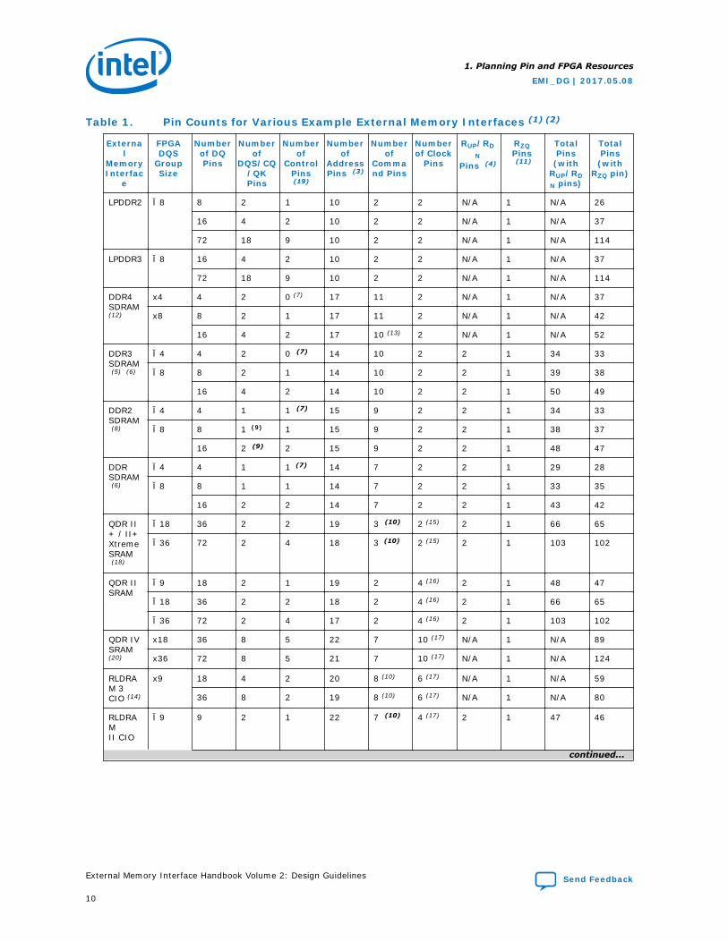
Table 1. Pin Counts for Various Example External Memory Interfaces (1) (2)
External
MemoryInterfac
e
FPGADQS
GroupSize
Numberof DQPins
Numberof
DQS/CQ/QKPins
Numberof
ControlPins(19)
Numberof
AddressPins (3)
Numberof
Command Pins
Numberof Clock
Pins
RUP/RDN
Pins (4)
RZQPins (11)
TotalPins(with
RUP/RDN pins)
TotalPins(with
RZQ pin)
LPDDR2 ×8 8 2 1 10 2 2 N/A 1 N/A 26
16 4 2 10 2 2 N/A 1 N/A 37
72 18 9 10 2 2 N/A 1 N/A 114
LPDDR3 ×8 16 4 2 10 2 2 N/A 1 N/A 37
72 18 9 10 2 2 N/A 1 N/A 114
DDR4SDRAM(12)
x4 4 2 0 (7) 17 11 2 N/A 1 N/A 37
x8 8 2 1 17 11 2 N/A 1 N/A 42
16 4 2 17 10 (13) 2 N/A 1 N/A 52
DDR3SDRAM (5) (6)
×4 4 2 0 (7) 14 10 2 2 1 34 33
×8 8 2 1 14 10 2 2 1 39 38
16 4 2 14 10 2 2 1 50 49
DDR2SDRAM (8)
×4 4 1 1 (7) 15 9 2 2 1 34 33
×8 8 1 (9) 1 15 9 2 2 1 38 37
16 2 (9) 2 15 9 2 2 1 48 47
DDRSDRAM (6)
×4 4 1 1 (7) 14 7 2 2 1 29 28
×8 8 1 1 14 7 2 2 1 33 35
16 2 2 14 7 2 2 1 43 42
QDR II+ / II+XtremeSRAM (18)
×18 36 2 2 19 3 (10) 2 (15) 2 1 66 65
×36 72 2 4 18 3 (10) 2 (15) 2 1 103 102
QDR IISRAM
×9 18 2 1 19 2 4 (16) 2 1 48 47
×18 36 2 2 18 2 4 (16) 2 1 66 65
×36 72 2 4 17 2 4 (16) 2 1 103 102
QDR IVSRAM(20)
x18 36 8 5 22 7 10 (17) N/A 1 N/A 89
x36 72 8 5 21 7 10 (17) N/A 1 N/A 124
RLDRAM 3CIO (14)
x9 18 4 2 20 8 (10) 6 (17) N/A 1 N/A 59
36 8 2 19 8 (10) 6 (17) N/A 1 N/A 80
RLDRAMII CIO
×9 9 2 1 22 7 (10) 4 (17) 2 1 47 46
continued...
1. Planning Pin and FPGA Resources
EMI_DG | 2017.05.08
External Memory Interface Handbook Volume 2: Design Guidelines Send Feedback
10
External
MemoryInterfac
e
FPGADQS
GroupSize
Numberof DQPins
Numberof
DQS/CQ/QKPins
Numberof
ControlPins(19)
Numberof
AddressPins (3)
Numberof
Command Pins
Numberof Clock
Pins
RUP/RDN
Pins (4)
RZQPins (11)
TotalPins(with
RUP/RDN pins)
TotalPins(with
RZQ pin)
18 4 1 21 7 (10) 4 (17) 2 1 57 56
×18 36 4 1 20 7 (10) 6 (17) 2 1 76 75
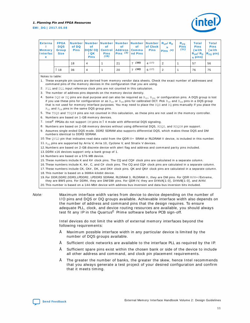
Notes to table:1. These example pin counts are derived from memory vendor data sheets. Check the exact number of addresses and
command pins of the memory devices in the configuration that you are using.2. PLL and DLL input reference clock pins are not counted in this calculation.3. The number of address pins depends on the memory device density.4. Some DQS or DQ pins are dual purpose and can also be required as RUP, RDN, or configuration pins. A DQS group is lost
if you use these pins for configuration or as RUP or RDN pins for calibrated OCT. Pick RUP and RDN pins in a DQS groupthat is not used for memory interface purposes. You may need to place the DQS and DQ pins manually if you place theRUP and RDN pins in the same DQS group pins.
5. The TDQS and TDQS# pins are not counted in this calculation, as these pins are not used in the memory controller.6. Numbers are based on 1-GB memory devices.7. Intel® FPGAs do not support DM pins in ×4 mode with differential DQS signaling.8. Numbers are based on 2-GB memory devices without using differential DQS, RDQS, and RDQS# pin support.9. Assumes single ended DQS mode. DDR2 SDRAM also supports differential DQS, which makes these DQS and DM
numbers identical to DDR3 SDRAM.10.The QVLD pin that indicates read data valid from the QDR II+ SRAM or RLDRAM II device, is included in this number.11.RZQ pins are supported by Arria V, Arria 10, Cyclone V, and Stratix V devices.12.Numbers are based on 2-GB discrete device with alert flag and address and command parity pins included.13.DDR4 x16 devices support only a bank group of 1.14.Numbers are based on a 576-MB device.15.These numbers include K and K# clock pins. The CQ and CQ# clock pins are calculated in a separate column.16.These numbers include K, K#, C, and C# clock pins. The CQ and CQ# clock pins are calculated in a separate column.17.These numbers include CK, CK#, DK, and DK# clock pins. QK and QK# clock pins are calculated in a separate column.18.This number is based on a 36864-kilobit device.19.For DDR,DDR2,DDR3,LPDDR2, LPDDR3 SDRAM, RLDRAM 3, RLDRAM II, they are DM pins. For QDR II/II+/Extreme,
they are BWS pins. For DDR4, they are DM/DBI pins. For QDR IV, they are DINVA[1:0], DINVB[1:0], and AINV.20.This number is based on a 144-Mbit device with address bus inversion and data bus inversion bits included.
Note: Maximum interface width varies from device to device depending on the number ofI/O pins and DQS or DQ groups available. Achievable interface width also depends onthe number of address and command pins that the design requires. To ensureadequate PLL, clock, and device routing resources are available, you should alwaystest fit any IP in the Quartus® Prime software before PCB sign-off.
Intel devices do not limit the width of external memory interfaces beyond thefollowing requirements:
• Maximum possible interface width in any particular device is limited by thenumber of DQS groups available.
• Sufficient clock networks are available to the interface PLL as required by the IP.
• Sufficient spare pins exist within the chosen bank or side of the device to includeall other address and command, and clock pin placement requirements.
• The greater the number of banks, the greater the skew, hence Intel recommendsthat you always generate a test project of your desired configuration and confirmthat it meets timing.
1. Planning Pin and FPGA Resources
EMI_DG | 2017.05.08
Send Feedback External Memory Interface Handbook Volume 2: Design Guidelines
11
1.1.1. Estimating Pin Requirements
You should use the Quartus Prime software for final pin fitting. However, you canestimate whether you have enough pins for your memory interface using the EMIFDevice Selector (for Arria 10 and Stratix 10 devices) on www.altera.com, or by thefollowing steps:
1. Find out how many read data pins are associated per read data strobe or clockpair, to determine which column of the DQS and DQ group availability (×4, ×8/×9,×16/×18, or ×32/×36) refer to the pin table.
2. Check the device density and package offering information to see if you canimplement the interface in one I/O bank or on one side or on two adjacent sides.
Note: If you target Arria II GX devices and you do not have enough I/O pins tohave the memory interface on one side of the device, you may place themon the other side of the device. Arria II GX devices allow a memoryinterface to span across the top and bottom, or left and right sides of thedevice. For any interface that spans across two different sides, use thewraparound interface performance.
3. Calculate the number of other memory interface pins needed, including any otherclocks (write clock or memory system clock), address, command, RUP, RDN, RZQ,and any other pins to be connected to the memory components. Ensure you haveenough pins to implement the interface in one I/O bank or one side or on twoadjacent sides.
Note: a. The DQS groups in Arria II GX devices reside on I/O modules, eachconsisting of 16 I/O pins. You can only use a maximum of 12 pins perI/O modules when the pins are used as DQS or DQ pins or HSTL/SSTLoutput or HSTL/SSTL bidirectional pins. When counting the number ofavailable pins for the rest of your memory interface, ensure you do notcount the leftover four pins per I/O modules used for DQS, DQ, addressand command pins. The leftover four pins can be used as input pinsonly.
b. Refer to the device pin-out tables and look for the blank space in therelevant DQS group column to identify the four pins that cannot be usedin an I/O module for Arria II GX devices.
c. If you enable Ping Pong PHY, the IP core exposes two independentAvalon interfaces to user logic, and a single external memory interfaceof double the width for the data bus and the CS#, CKE, ODT, andCK/CK# signals. The rest remain as if in single interface configuration.
You should test the proposed pin-outs with the rest of your design in the QuartusPrime software (with the correct I/O standard and OCT connections) before finalizingthe pin-outs. There can be interactions between modules that are illegal in theQuartus Prime software that you might not know about unless you compile the designand use the Quartus Prime Pin Planner.
Related Information
External Memory Interface Device Selector
1. Planning Pin and FPGA Resources
EMI_DG | 2017.05.08
External Memory Interface Handbook Volume 2: Design Guidelines Send Feedback
12
1.1.2. DDR, DDR2, DDR3, and DDR4 SDRAM Clock Signals
DDR, DDR2, DDR3, and DDR4 SDRAM devices use CK and CK# signals to clock theaddress and command signals into the memory. Furthermore, the memory uses theseclock signals to generate the DQS signal during a read through the DLL inside thememory. The SDRAM data sheet specifies the following timings:
• tDQSCK is the skew between the CK or CK# signals and the SDRAM-generated DQSsignal
• tDSH is the DQS falling edge from CK rising edge hold time
• tDSS is the DQS falling edge from CK rising edge setup time
• tDQSS is the positive DQS latching edge to CK rising edge
SDRAM have a write requirement (tDQSS) that states the positive edge of the DQSsignal on writes must be within ± 25% (± 90°) of the positive edge of the SDRAMclock input. Therefore, you should generate the CK and CK# signals using the DDRregisters in the IOE to match with the DQS signal and reduce any variations acrossprocess, voltage, and temperature. The positive edge of the SDRAM clock, CK, isaligned with the DQS write to satisfy tDQSS.
DDR3 SDRAM can use a daisy-chained control address command (CAC) topology, inwhich the memory clock must arrive at each chip at a different time. To compensatefor the flight-time skew between devices when using the CAC topology, you shouldemploy write leveling.
1.1.3. DDR, DDR2, DDR3, and DDR4 SDRAM Command and AddressSignals
Command and address signals in SDRAM devices are clocked into the memory deviceusing the CK or CK# signal. These pins operate at single data rate (SDR) using onlyone clock edge. The number of address pins depends on the SDRAM device capacity.The address pins are multiplexed, so two clock cycles are required to send the row,column, and bank address.
For DDR, DDR2, and DDR3, the CS#, RAS#, CAS#, WE#, CKE, and ODT pins are SDRAMcommand and control pins. For DDR3 SDRAM, certain topologies such as RDIMM andLRDIMM include RESET#, PAR_IN (1.5V LVCMOS I/O standard), and ERR_OUT#(SSTL-15 I/O standard).
The DDR2 SDRAM command and address inputs do not have a symmetrical setup andhold time requirement with respect to the SDRAM clocks, CK, and CK#.
Although DDR4 operates in fundamentally the same way as other SDRAM, there areno longer dedicated pins for RAS#, CAS#, and WE#, as those are now shared withhigher-order address pins. DDR4 still has CS#, CKE, ODT, and RESET# pins, similar toDDR3. DDR4 introduces some additional pins, including the ACT# (activate) pin andBG (bank group) pins. Depending on the memory format and the functions enabled,the following pins might also exist in DDR4: PAR (address command parity) pin andthe ALERT# pin.
For Intel SDRAM high-performance controllers in Stratix III and Stratix IV devices, thecommand and address clock is a dedicated PLL clock output whose phase can beadjusted to meet the setup and hold requirements of the memory clock. Thecommand and address clock is also typically half-rate, although a full-rate
1. Planning Pin and FPGA Resources
EMI_DG | 2017.05.08
Send Feedback External Memory Interface Handbook Volume 2: Design Guidelines
13
implementation can also be created. The command and address pins use the DDIOoutput circuitry to launch commands from either the rising or falling edges of theclock. The chip select CS#, clock enable CKE, and ODT pins are only enabled for onememory clock cycle and can be launched from either the rising or falling edge of thecommand and address clock signal. The address and other command pins are enabledfor two memory clock cycles and can also be launched from either the rising or fallingedge of the command and address clock signal.
In Arria II GX devices, the command and address clock is either shared with thewrite_clk_2x or the mem_clk_2x clock.
1.1.4. DDR, DDR2, DDR3, and DDR4 SDRAM Data, Data Strobes, DM/DBI,and Optional ECC Signals
DDR SDRAM uses bidirectional single-ended data strobe (DQS); DDR3 and DDR4SDRAM use bidirectional differential data strobes. The DQSn pins in DDR2 SDRAMdevices are optional but recommended for DDR2 SDRAM designs operating at morethan 333 MHz. Differential DQS operation enables improved system timing due toreduced crosstalk and less simultaneous switching noise on the strobe output drivers.The DQ pins are also bidirectional.
Regardless of interface width, DDR SDRAM always operates in ×8 mode DQS groups.DQ pins in DDR2, DDR3, and DDR4 SDRAM interfaces can operate in either ×4 or ×8mode DQS groups, depending on your chosen memory device or DIMM, regardless ofinterface width. The ×4 and ×8 configurations use one pair of bidirectional data strobesignals, DQS and DQSn, to capture input data. However, two pairs of data strobes,UDQS and UDQS# (upper byte) and LDQS and LDQS# (lower byte), are required bythe ×16 configuration devices. A group of DQ pins must remain associated with itsrespective DQS and DQSn pins.
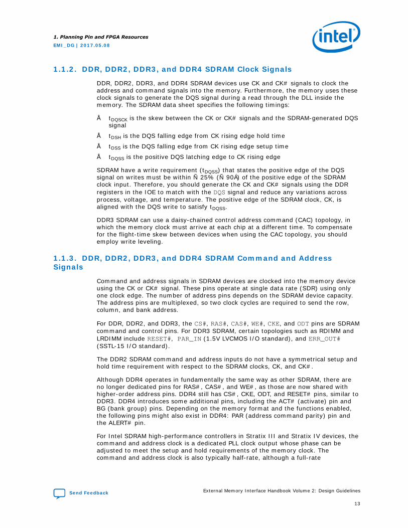
The DQ signals are edge-aligned with the DQS signal during a read from the memoryand are center-aligned with the DQS signal during a write to the memory. Thememory controller shifts the DQ signals by –90 degrees during a write operation tocenter align the DQ and DQS signals. The PHY IP delays the DQS signal during a read,so that the DQ and DQS signals are center aligned at the capture register. Inteldevices use a phase-locked loop (PLL) to center-align the DQS signal with respect tothe DQ signals during writes and Intel devices use dedicated DQS phase-shift circuitryto shift the incoming DQS signal during reads. The following figure shows an examplewhere the DQS signal is shifted by 90 degrees for a read from the DDR2 SDRAM.
Figure 1. Edge-aligned DQ and DQS Relationship During a DDR2 SDRAM Read in Burst-of-Four Mode
DQS at DQIOE registers
DQS at FPGA Pin
DQ at DQIOE registers
DQ atFPGA Pin
DQS phase shift
Preamble Postamble
1. Planning Pin and FPGA Resources
EMI_DG | 2017.05.08
External Memory Interface Handbook Volume 2: Design Guidelines Send Feedback
14
The following figure shows an example of the relationship between the data and datastrobe during a burst-of-four write.
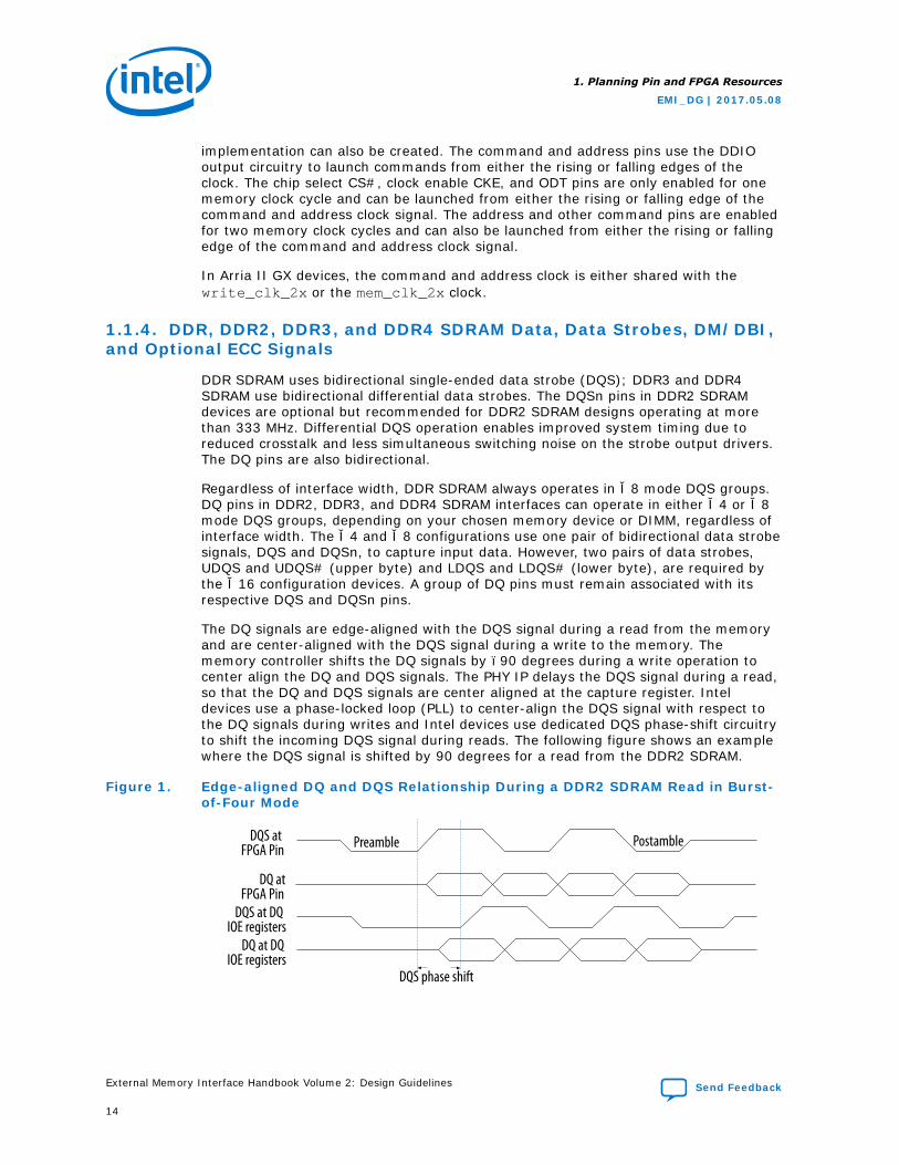
Figure 2. DQ and DQS Relationship During a DDR2 SDRAM Write in Burst-of-Four Mode
DQS atFPGA Pin
DQ atFPGA Pin
The memory device's setup (tDS) and hold times (tDH) for the DQ and DM pins duringwrites are relative to the edges of DQS write signals and not the CK or CK# clock.Setup and hold requirements are not necessarily balanced inDDR2 and DDR3 SDRAM,unlike in DDR SDRAM devices.
The DQS signal is generated on the positive edge of the system clock to meet thetDQSS requirement. DQ and DM signals use a clock shifted –90 degrees from thesystem clock, so that the DQS edges are centered on the DQ or DM signals when theyarrive at the DDR2 SDRAM. The DQS, DQ, and DM board trace lengths need to betightly matched (within 20 ps).
The SDRAM uses the DM pins during a write operation. Driving the DM pins low showsthat the write is valid. The memory masks the DQ signals if the DM pins are drivenhigh. To generate the DM signal, Intel recommends that you use the spare DQ pinwithin the same DQS group as the respective data, to minimize skew.
The DM signal's timing requirements at the SDRAM input are identical to those for DQdata. The DDR registers, clocked by the –90 degree shifted clock, create the DMsignals.
DDR4 supports DM similarly to other SDRAM, except that in DDR4 DM is active LOWand bidirectional, because it supports Data Bus Inversion (DBI) through the same pin.DM is multiplexed with DBI by a Mode Register setting whereby only one function canbe enabled at a time. DBI is an input/output identifying whether to store/output thetrue or inverted data. When enabled, if DBI is LOW, during a write operation the datais inverted and stored inside the DDR4 SDRAM; during a read operation, the data isinverted and output. The data is not inverted if DBI is HIGH. For Arria 10, the DBI (forDDR4) and the DM (for DDR3) pins in each DQS group must be paired with a DQ pinfor proper operation.
Some SDRAM modules support error correction coding (ECC) to allow the controller todetect and automatically correct error in data transmission. The 72-bit SDRAMmodules contain eight extra data pins in addition to 64 data pins. The eight extra ECCpins should be connected to a single DQS or DQ group on the FPGA.
1.1.5. DDR, DDR2, DDR3, and DDR4 SDRAM DIMM Options
Unbuffered DIMMs (UDIMMs) require one set of chip-select (CS#), on-die termination(ODT), clock-enable (CKE), and clock pair (CK/CKn) for every physical rank on theDIMM. Registered DIMMs use only one pair of clocks. DDR3 registered DIMMs requirea minimum of two chip-select signals, while DDR4 requires only one.
1. Planning Pin and FPGA Resources
EMI_DG | 2017.05.08
Send Feedback External Memory Interface Handbook Volume 2: Design Guidelines
15
Compared to the unbuffered DIMMs (UDIMM), registered and load-reduced DIMMs(RDIMMs and LRDIMMs, respectively) use at least two chip-select signals CS#[1:0] inDDR3 and DDR4. Both RDIMMs and LRDIMMs require an additional parity signal foraddress, RAS#, CAS#, and WE# signals. A parity error signal is asserted by the modulewhenever a parity error is detected.
LRDIMMs expand on the operation of RDIMMs by buffering the DQ/DQS bus. Only oneelectrical load is presented to the controller regardless of the number of ranks,therefore only one clock enable (CKE) and ODT signal are required for LRDIMMs,regardless of the number of physical ranks. Because the number of physical ranksmay exceed the number of physical chip-select signals, DDR3 LRDIMMs provide afeature known as rank multiplication, which aggregates two or four physical ranks intoone larger logical rank. Refer to LRDIMM buffer documentation for details on rankmultiplication.
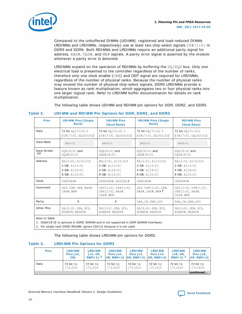
The following table shows UDIMM and RDIMM pin options for DDR, DDR2, and DDR3.
Table 2. UDIMM and RDIMM Pin Options for DDR, DDR2, and DDR3
Pins UDIMM Pins (SingleRank)
UDIMM Pins(Dual Rank)
RDIMM Pins (SingleRank)
RDIMM Pins(Dual Rank)
Data 72 bit DQ[71:0] =CB[7:0], DQ[63:0]
72 bit DQ[71:0] =CB[7:0], DQ[63:0]
72 bit DQ[71:0] =CB[7:0], DQ[63:0]
72 bit DQ[71:0]=CB[7:0], DQ[63:0]
Data Mask DM[8:0] DM[8:0] DM[8:0] DM[8:0]
Data Strobe (1)
DQS[8:0] andDQS#[8:0]
DQS[8:0] andDQS#[8:0]
DQS[8:0] andDQS#[8:0]
DQS[8:0] andDQS#[8:0]
Address BA[2:0], A[15:0]–2 GB: A[13:0]4 GB: A[14:0]8 GB: A[15:0]
BA[2:0], A[15:0]–2 GB: A[13:0]4 GB: A[14:0]8 GB: A[15:0]
BA[2:0], A[15:0]–2 GB: A[13:0]4 GB: A[14:0]8 GB: A[15:0]
BA[2:0], A[15:0]–2 GB: A[13:0]4 GB: A[14:0]8 GB: A[15:0]
Clock CK0/CK0# CK0/CK0#, CK1/CK1# CK0/CK0# CK0/CK0#
Command ODT, CS#, CKE, RAS#,CAS#, WE#
ODT[1:0], CS#[1:0],CKE[1:0], RAS#,CAS#, WE#
ODT, CS#[1:0], CKE,RAS#, CAS#, WE# 2
ODT[1:0], CS#[1:0],CKE[1:0], RAS#,CAS#, WE#
Parity — — PAR_IN, ERR_OUT PAR_IN, ERR_OUT
Other Pins SA[2:0], SDA, SCL,EVENT#, RESET#
SA[2:0], SDA, SCL,EVENT#, RESET#
SA[2:0], SDA, SCL,EVENT#, RESET#
SA[2:0], SDA, SCL,EVENT#, RESET#
Note to Table:1. DQS#[8:0] is optional in DDR2 SDRAM and is not supported in DDR SDRAM interfaces.2. For single rank DDR2 RDIMM, ignore CS#[1] because it is not used.
The following table shows LRDIMM pin options for DDR3.
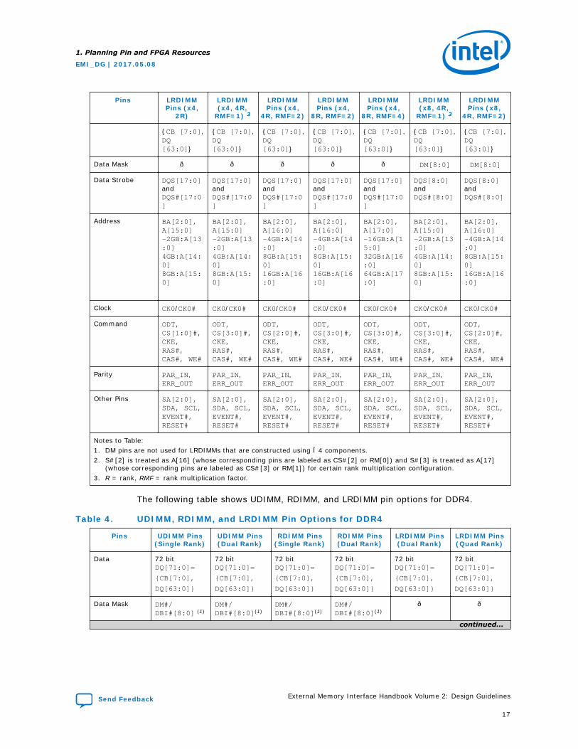
Table 3. LRDIMM Pin Options for DDR3
Pins LRDIMMPins (x4,
2R)
LRDIMM(x4, 4R,
RMF=1) 3
LRDIMMPins (x4,
4R, RMF=2)
LRDIMMPins (x4,
8R, RMF=2)
LRDIMMPins (x4,
8R, RMF=4)
LRDIMM(x8, 4R,
RMF=1) 3
LRDIMMPins (x8,
4R, RMF=2)
Data 72 bit DQ[71:0]=
72 bit DQ[71:0]=
72 bit DQ[71:0]=
72 bit DQ[71:0]=
72 bit DQ[71:0]=
72 bit DQ[71:0]=
72 bit DQ[71:0]=
continued...
1. Planning Pin and FPGA Resources
EMI_DG | 2017.05.08
External Memory Interface Handbook Volume 2: Design Guidelines Send Feedback
16
Pins LRDIMMPins (x4,
2R)
LRDIMM(x4, 4R,
RMF=1) 3
LRDIMMPins (x4,
4R, RMF=2)
LRDIMMPins (x4,
8R, RMF=2)
LRDIMMPins (x4,
8R, RMF=4)
LRDIMM(x8, 4R,
RMF=1) 3
LRDIMMPins (x8,
4R, RMF=2)
CB [7:0],DQ[63:0]
CB [7:0],DQ[63:0]
CB [7:0],DQ[63:0]
CB [7:0],DQ[63:0]
CB [7:0],DQ[63:0]
CB [7:0],DQ[63:0]
CB [7:0],DQ[63:0]
Data Mask — — — — — DM[8:0] DM[8:0]
Data Strobe DQS[17:0]andDQS#[17:0]
DQS[17:0]andDQS#[17:0]
DQS[17:0]andDQS#[17:0]
DQS[17:0]andDQS#[17:0]
DQS[17:0]andDQS#[17:0]
DQS[8:0]andDQS#[8:0]
DQS[8:0]andDQS#[8:0]
Address BA[2:0], A[15:0]-2GB:A[13:0] 4GB:A[14:0]8GB:A[15:0]
BA[2:0], A[15:0]-2GB:A[13:0] 4GB:A[14:0]8GB:A[15:0]
BA[2:0], A[16:0]-4GB:A[14:0] 8GB:A[15:0]16GB:A[16:0]
BA[2:0], A[16:0]-4GB:A[14:0] 8GB:A[15:0]16GB:A[16:0]
BA[2:0], A[17:0]-16GB:A[15:0] 32GB:A[16:0]64GB:A[17:0]
BA[2:0], A[15:0]-2GB:A[13:0] 4GB:A[14:0]8GB:A[15:0]
BA[2:0], A[16:0]-4GB:A[14:0] 8GB:A[15:0]16GB:A[16:0]
Clock CK0/CK0# CK0/CK0# CK0/CK0# CK0/CK0# CK0/CK0# CK0/CK0# CK0/CK0#
Command ODT,CS[1:0]#,CKE,RAS#,CAS#, WE#
ODT,CS[3:0]#,CKE,RAS#,CAS#, WE#
ODT,CS[2:0]#,CKE,RAS#,CAS#, WE#
ODT,CS[3:0]#,CKE,RAS#,CAS#, WE#
ODT,CS[3:0]#,CKE,RAS#,CAS#, WE#
ODT,CS[3:0]#,CKE,RAS#,CAS#, WE#
ODT,CS[2:0]#,CKE,RAS#,CAS#, WE#
Parity PAR_IN,ERR_OUT
PAR_IN,ERR_OUT
PAR_IN,ERR_OUT
PAR_IN,ERR_OUT
PAR_IN,ERR_OUT
PAR_IN,ERR_OUT
PAR_IN,ERR_OUT
Other Pins SA[2:0],SDA, SCL,EVENT#,RESET#
SA[2:0],SDA, SCL,EVENT#,RESET#
SA[2:0],SDA, SCL,EVENT#,RESET#
SA[2:0],SDA, SCL,EVENT#,RESET#
SA[2:0],SDA, SCL,EVENT#,RESET#
SA[2:0],SDA, SCL,EVENT#,RESET#
SA[2:0],SDA, SCL,EVENT#,RESET#
Notes to Table:1. DM pins are not used for LRDIMMs that are constructed using ×4 components.2. S#[2] is treated as A[16] (whose corresponding pins are labeled as CS#[2] or RM[0]) and S#[3] is treated as A[17]
(whose corresponding pins are labeled as CS#[3] or RM[1]) for certain rank multiplication configuration.3. R = rank, RMF = rank multiplication factor.
The following table shows UDIMM, RDIMM, and LRDIMM pin options for DDR4.
Table 4. UDIMM, RDIMM, and LRDIMM Pin Options for DDR4
Pins UDIMM Pins(Single Rank)
UDIMM Pins(Dual Rank)
RDIMM Pins(Single Rank)
RDIMM Pins(Dual Rank)
LRDIMM Pins(Dual Rank)
LRDIMM Pins(Quad Rank)
Data 72 bitDQ[71:0]=
CB[7:0],
DQ[63:0]
72 bitDQ[71:0]=
CB[7:0],
DQ[63:0]
72 bitDQ[71:0]=
CB[7:0],
DQ[63:0]
72 bitDQ[71:0]=
CB[7:0],
DQ[63:0]
72 bitDQ[71:0]=
CB[7:0],
DQ[63:0]
72 bitDQ[71:0]=
CB[7:0],
DQ[63:0]
Data Mask DM#/DBI#[8:0] (1)
DM#/DBI#[8:0](1)
DM#/DBI#[8:0](1)
DM#/DBI#[8:0](1)
— —
continued...
1. Planning Pin and FPGA Resources
EMI_DG | 2017.05.08
Send Feedback External Memory Interface Handbook Volume 2: Design Guidelines
17
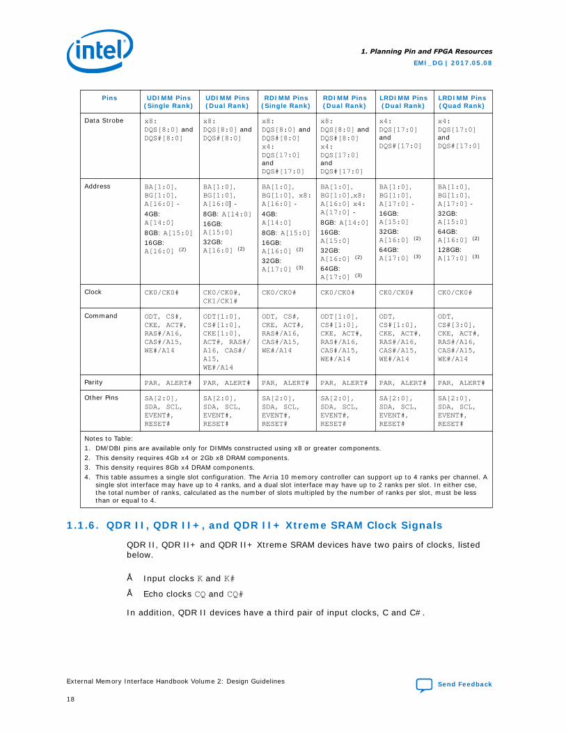
Pins UDIMM Pins(Single Rank)
UDIMM Pins(Dual Rank)
RDIMM Pins(Single Rank)
RDIMM Pins(Dual Rank)
LRDIMM Pins(Dual Rank)
LRDIMM Pins(Quad Rank)
Data Strobe x8:DQS[8:0] andDQS#[8:0]
x8:DQS[8:0] andDQS#[8:0]
x8:DQS[8:0] andDQS#[8:0]x4:DQS[17:0]andDQS#[17:0]
x8:DQS[8:0] andDQS#[8:0]x4:DQS[17:0]andDQS#[17:0]
x4:DQS[17:0]andDQS#[17:0]
x4:DQS[17:0]andDQS#[17:0]
Address BA[1:0],BG[1:0],A[16:0] -4GB:A[14:0]
8GB: A[15:0]16GB:A[16:0] (2)
BA[1:0],BG[1:0],A[16:0] -8GB: A[14:0]16GB:A[15:0]
32GB:A[16:0] (2)
BA[1:0],BG[1:0], x8:A[16:0] -4GB:A[14:0]
8GB: A[15:0]16GB:A[16:0] (2)
32GB:A[17:0] (3)
BA[1:0],BG[1:0],x8:A[16:0] x4:A[17:0] -8GB: A[14:0]16GB:A[15:0]
32GB:A[16:0] (2)
64GB:A[17:0] (3)
BA[1:0],BG[1:0],A[17:0] -16GB:A[15:0]
32GB:A[16:0] (2)
64GB:A[17:0] (3)
BA[1:0],BG[1:0],A[17:0] -32GB:A[15:0]
64GB:A[16:0] (2)
128GB:A[17:0] (3)
Clock CK0/CK0# CK0/CK0#,CK1/CK1#
CK0/CK0# CK0/CK0# CK0/CK0# CK0/CK0#
Command ODT, CS#,CKE, ACT#,RAS#/A16,CAS#/A15,WE#/A14
ODT[1:0],CS#[1:0],CKE[1:0],ACT#, RAS#/A16, CAS#/A15,WE#/A14
ODT, CS#,CKE, ACT#,RAS#/A16,CAS#/A15,WE#/A14
ODT[1:0],CS#[1:0],CKE, ACT#,RAS#/A16,CAS#/A15,WE#/A14
ODT,CS#[1:0],CKE, ACT#,RAS#/A16,CAS#/A15,WE#/A14
ODT,CS#[3:0],CKE, ACT#,RAS#/A16,CAS#/A15,WE#/A14
Parity PAR, ALERT# PAR, ALERT# PAR, ALERT# PAR, ALERT# PAR, ALERT# PAR, ALERT#
Other Pins SA[2:0],SDA, SCL,EVENT#,RESET#
SA[2:0],SDA, SCL,EVENT#,RESET#
SA[2:0],SDA, SCL,EVENT#,RESET#
SA[2:0],SDA, SCL,EVENT#,RESET#
SA[2:0],SDA, SCL,EVENT#,RESET#
SA[2:0],SDA, SCL,EVENT#,RESET#
Notes to Table:1. DM/DBI pins are available only for DIMMs constructed using x8 or greater components.2. This density requires 4Gb x4 or 2Gb x8 DRAM components.3. This density requires 8Gb x4 DRAM components.4. This table assumes a single slot configuration. The Arria 10 memory controller can support up to 4 ranks per channel. A
single slot interface may have up to 4 ranks, and a dual slot interface may have up to 2 ranks per slot. In either cse,the total number of ranks, calculated as the number of slots multipled by the number of ranks per slot, must be lessthan or equal to 4.
1.1.6. QDR II, QDR II+, and QDR II+ Xtreme SRAM Clock Signals
QDR II, QDR II+ and QDR II+ Xtreme SRAM devices have two pairs of clocks, listedbelow.
• Input clocks K and K#
• Echo clocks CQ and CQ#
In addition, QDR II devices have a third pair of input clocks, C and C#.
1. Planning Pin and FPGA Resources
EMI_DG | 2017.05.08
External Memory Interface Handbook Volume 2: Design Guidelines Send Feedback
18
The positive input clock, K, is the logical complement of the negative input clock, K#.Similarly, C and CQ are complements of C# and CQ#, respectively. With thesecomplementary clocks, the rising edges of each clock leg latch the DDR data.
The QDR II SRAM devices use the K and K# clocks for write access and the C and C#clocks for read accesses only when interfacing more than one QDR II SRAM device.Because the number of loads that the K and K# clocks drive affects the switchingtimes of these outputs when a controller drives a single QDR II SRAM device, C andC# are unnecessary. This is because the propagation delays from the controller to theQDR II SRAM device and back are the same. Therefore, to reduce the number of loadson the clock traces, QDR II SRAM devices have a single-clock mode, and the K and K#clocks are used for both reads and writes. In this mode, the C and C# clocks are tiedto the supply voltage (VDD). Intel FPGA external memory IP supports only single-clockmode.
For QDR II, QDR II+, or QDR II+ Xtreme SRAM devices, the rising edge of K is used tocapture synchronous inputs to the device and to drive out data through Q[x:0], insimilar fashion to QDR II SRAM devices in single clock mode. All accesses are initiatedon the rising edge of K .
CQ and CQ# are the source-synchronous output clocks from the QDR II, QDR II+, orQDR II+ Xtreme SRAM device that accompanies the read data.
The Intel device outputs the K and K# clocks, data, address, and command lines to theQDR II, QDR II+, or QDR II+ Xtreme SRAM device. For the controller to operateproperly, the write data (D), address (A), and control signal trace lengths (andtherefore the propagation times) should be equal to the K and K# clock trace lengths.
You can generate K and K# clocks using any of the PLL registers via the DDR registers.Because of strict skew requirements between K and K# signals, use adjacent pins togenerate the clock pair. The propagation delays for K and K# from the FPGA to theQDR II, QDR II+, or QDR II+ Xtreme SRAM device are equal to the delays on the dataand address (D, A) signals. Therefore, the signal skew effect on the write and readrequest operations is minimized by using identical DDR output circuits to generateclock and data inputs to the memory.
1.1.7. QDR II, QDR II+ and QDR II+ Xtreme SRAM Command Signals
QDR II, QDR II+ and QDR II+ Xtreme SRAM devices use the write port select (WPS#)signal to control write operations and the read port select (RPS#) signal to controlread operations.
1.1.8. QDR II, QDR II+ and QDR II+ Xtreme SRAM Address Signals
QDR II, QDR II+ and QDR II+ Xtreme SRAM devices use one address bus (A) for bothread and write accesses.
1. Planning Pin and FPGA Resources
EMI_DG | 2017.05.08
Send Feedback External Memory Interface Handbook Volume 2: Design Guidelines
19
1.1.9. QDR II, QDR II+ and QDR II+ Xtreme SRAM Data, BWS, and QVLDSignals
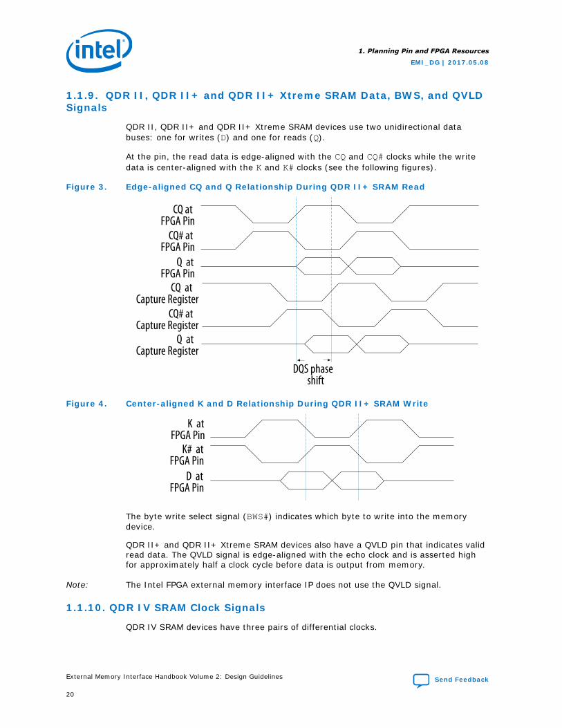
QDR II, QDR II+ and QDR II+ Xtreme SRAM devices use two unidirectional databuses: one for writes (D) and one for reads (Q).
At the pin, the read data is edge-aligned with the CQ and CQ# clocks while the writedata is center-aligned with the K and K# clocks (see the following figures).
Figure 3. Edge-aligned CQ and Q Relationship During QDR II+ SRAM Read
CQ# at FPGA Pin
CQ at FPGA Pin
Q at FPGA Pin
CQ at Capture Register
CQ# at Capture Register
Q at Capture Register
DQS phase shift
Figure 4. Center-aligned K and D Relationship During QDR II+ SRAM Write
K# at FPGA Pin
K at FPGA Pin
D at FPGA Pin
The byte write select signal (BWS#) indicates which byte to write into the memorydevice.
QDR II+ and QDR II+ Xtreme SRAM devices also have a QVLD pin that indicates validread data. The QVLD signal is edge-aligned with the echo clock and is asserted highfor approximately half a clock cycle before data is output from memory.
Note: The Intel FPGA external memory interface IP does not use the QVLD signal.
1.1.10. QDR IV SRAM Clock Signals
QDR IV SRAM devices have three pairs of differential clocks.
1. Planning Pin and FPGA Resources
EMI_DG | 2017.05.08
External Memory Interface Handbook Volume 2: Design Guidelines Send Feedback
20
The three QDR IV differential clocks are as follows:
• Address and Command Input Clocks CK and CK#
• Data Input Clocks DKx and DKx#, where x can be A or B, referring to therespective ports
• Data Output Clocks, QKx and QKx#, where x can be A or B, referring to therespective ports
QDR IV SRAM devices have two independent bidirectional data ports, Port A and PortB, to support concurrent read/write transactions on both ports. These data ports arecontrolled by a common address port clocked by CK and CK# in double data rate.There is one pair of CK and CK# pins per QDR IV SRAM device.
DKx and DKx# samples the DQx inputs on both rising and falling edges. Similarly, QKxand QKx# samples the DQx outputs on both rising and falling edges.
QDR IV SRAM devices employ two sets of free running differential clocks toaccompany the data. The DKx and DKx# clocks are the differential input data clocksused during writes. The QKx and QKx# clocks are the output data clocks used duringreads. Each pair of DKx and DKx#, or QKx and QKx# clocks are associated with either9 or 18 data bits.
The polarity of the QKB and QKB# pins in the Intel FPGA external memory interface IPwas swapped with respect to the polarity of the differential input buffer on the FPGA.In other words, the QKB pins on the memory side must be connected to the negativepins of the input buffers on the FPGA side, and the QKB# pins on the memory sidemust be connected to the positive pins of the input buffers on the FPGA side. Noticethat the port names at the top-level of the IP already reflect this swap (that is,mem_qkb is assigned to the negative buffer leg, and mem_qkb_n is assigned to thepositive buffer leg).
QDR IV SRAM devices are available in x18 and x36 bus width configurations. Theexact clock-data relationships are as follows:
• For ×18 data bus width configuration, there are 9 data bits associated with eachpair of write and read clocks. So, there are two pairs of DKx and DKx# pins andtwo pairs of QKx or QKx# pins.
• For ×36 data bus width configuration, there are 18 data bits associated with eachpair of write and read clocks. So, there are two pairs of DKx and DKx# pins andtwo pairs of QKx or QKx# pins.
There are tCKDK timing requirements for skew between CK and DKx or CK# andDKx# .Similarly, there are tCKQK timing requirements for skew between CK and QKxor CK# and QKx# .
1.1.11. QDR IV SRAM Commands and Addresses, AP, and AINV Signals
The CK and CK# signals clock the commands and addresses into the memory devices.There is one pair of CK and CK# pins per QDR IV SRAM device. These pins operate atdouble data rate using both rising and falling edge. The rising edge of CK latches theaddresses for port A, while the falling edge of CK latches the addresses inputs for portB.
1. Planning Pin and FPGA Resources
EMI_DG | 2017.05.08
Send Feedback External Memory Interface Handbook Volume 2: Design Guidelines
21
QDR IV SRAM devices have the ability to invert all address pins to reduce potentialsimultaneous switching noise. Such inversion is accomplished using the AddressInversion Pin for Address and Address Parity Inputs (AINV), whichassumes an address parity of 0, and indicates whether the address bus and addressparity are inverted.
The above features are available as Option Control under Configuration RegisterSettings in Arria 10 EMIF IP. The commands and addresses must meet the memoryaddress and command setup (tAS, tCS) and hold (tAH, tCH) time requirements.
1.1.12. QDR IV SRAM Data, DINV, and QVLD Signals
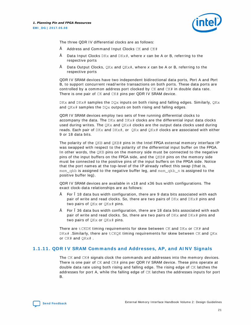
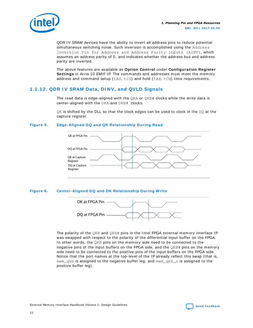
The read data is edge-aligned with the QKA or QKB# clocks while the write data iscenter-aligned with the DKA and DKB# clocks.
QK is shifted by the DLL so that the clock edges can be used to clock in the DQ at thecapture register.
Figure 5. Edge-Aligned DQ and QK Relationship During Read
QK at FPGA Pin
DQ at FPGA Pin
QK at Capture RegisterDQ at CaptureRegister
Figure 6. Center-Aligned DQ and DK Relationship During Write
DK at FPGA Pin
DQ at FPGA Pin
The polarity of the QKB and QKB# pins in the Intel FPGA external memory interface IPwas swapped with respect to the polarity of the differential input buffer on the FPGA.In other words, the QKB pins on the memory side need to be connected to thenegative pins of the input buffers on the FPGA side, and the QKB# pins on the memoryside need to be connected to the positive pins of the input buffers on the FPGA side.Notice that the port names at the top-level of the IP already reflect this swap (that is,mem_qkb is assigned to the negative buffer leg, and mem_qkb_n is assigned to thepositive buffer leg).
1. Planning Pin and FPGA Resources
EMI_DG | 2017.05.08
External Memory Interface Handbook Volume 2: Design Guidelines Send Feedback
22
The synchronous read/write input, RWx#, is used in conjunction with the synchronousload input, LDx#, to indicate a Read or Write Operation. For port A, these signals aresampled on the rising edge of CK clock, for port B, these signals are sampled on thefalling edge of CK clock.
QDR IV SRAM devices have the ability to invert all data pins to reduce potentialsimultaneous switching noise, using the Data Inversion Pin for DQ Data Bus, DINVx.This pin indicates whether DQx pins are inverted or not.
To enable the data pin inversion feature, click Configuration Register Settings Option Control in the Arria 10 or Stratix 10 EMIF IP.
QDR IV SRAM devices also have a QVLD pin which indicates valid read data. The QVLDsignal is edge-aligned with QKx or QKx# and is high approximately one-half clock cyclebefore data is output from the memory.
Note: The Intel ZFPGA external memory interface IP does not use the QVLD signal.
1.1.13. RLDRAM II and RLDRAM 3 Clock Signals
RLDRAM II and RLDRAM 3 devices use CK and CK# signals to clock the command andaddress bus in single data rate (SDR). There is one pair of CK and CK# pins perRLDRAM II or RLDRAM 3 device.
Instead of a strobe, RLDRAM II and RLDRAM 3 devices use two sets of free-runningdifferential clocks to accompany the data. The DK and DK# clocks are the differentialinput data clocks used during writes while the QK or QK# clocks are the output dataclocks used during reads. Even though QK and QK# signals are not differential signalsaccording to the RLDRAM II and RLDRAM 3 data sheets, Micron treats these signals assuch for their testing and characterization. Each pair of DK and DK#, or QK and QK#clocks are associated with either 9 or 18 data bits.
The exact clock-data relationships are as follows:
• RLDRAM II: For ×36 data bus width configuration, there are 18 data bitsassociated with each pair of write and read clocks. So, there are two pairs of DKand DK# pins and two pairs of QK or QK# pins.
• RLDRAM 3: For ×36 data bus width configuration, there are 18 data bitsassociated with each pair of write clocks. There are 9 data bits associated witheach pair of read clocks. So, there are two pairs of DK and DK# pins and four pairsof QK and QK# pins.
• RLDRAM II: For ×18 data bus width configuration, there are 18 data bits per onepair of write clocks and nine data bits per one pair of read clocks. So, there is onepair of DK and DK# pins, but there are two pairs of QK and QK# pins.
• RLDRAM 3: For ×18 data bus width configuration, there are 9 data bits per onepair of write clocks and nine data bits per one pair of read clocks. So, there aretwo pairs of DK and DK# pins, and two pairs of QK and QK# pins
• RLDRAM II: For ×9 data bus width configuration, there are nine data bitsassociated with each pair of write and read clocks. So, there is one pair of DK andDK# pins and one pair of QK and QK# pins each.
• RLDRAM 3: RLDRAM 3 does not have the ×9 data bus width configuration.
1. Planning Pin and FPGA Resources
EMI_DG | 2017.05.08
Send Feedback External Memory Interface Handbook Volume 2: Design Guidelines
23
There are tCKDK timing requirements for skew between CK and DK or CK# and DK#.
For both RLDRAM II and RLDRAM 3, because of the loads on these I/O pins, themaximum frequency you can achieve depends on the number of memory devices youare connecting to the Intel device. Perform SPICE or IBIS simulations to analyze theloading effects of the pin-pair on multiple RLDRAM II or RLDRAM 3 devices.
1.1.14. RLDRAM II and RLDRAM 3 Commands and Addresses
The CK and CK# signals clock the commands and addresses into the memory devices.
These pins operate at single data rate using only one clock edge. RLDRAM II andRLDRAM 3 support both non-multiplexed and multiplexed addressing. Multiplexedaddressing allows you to save a few user I/O pins while non-multiplexed addressingallows you to send the address signal within one clock cycle instead of two clockcycles. CS#, REF#, and WE# pins are input commands to the RLDRAM II or RLDRAM 3device.
The commands and addresses must meet the memory address and command setup(tAS, tCS) and hold (tAH, tCH) time requirements.
Note: The RLDRAM II and RLDRAM 3 external memory interface IP do not supportmultiplexed addressing.
1.1.15. RLDRAM II and RLDRAM 3 Data, DM and QVLD Signals
The read data is edge-aligned with the QK or QK# clocks while the write data iscenter-aligned with the DK and DK# clocks (see the following figures). The memorycontroller shifts the DK and DK# signals to center align the DQ and DK or DK# signalsduring a write. It also shifts the QK signal during a read, so that the read data (DQsignals) and QK clock is center-aligned at the capture register.
Intel devices use dedicated DQS phase-shift circuitry to shift the incoming QK signalduring reads and use a PLL to center-align the DK and DK# signals with respect to theDQ signals during writes.
Figure 7. Edge-aligned DQ and QK Relationship During RLDRAM II or RLDRAM 3 Read
QK atFPGA Pin
DQ atFPGA Pin
QK at DQLE Registers
DQ at DQLE Registers
DQS Phase Shift
1. Planning Pin and FPGA Resources
EMI_DG | 2017.05.08
External Memory Interface Handbook Volume 2: Design Guidelines Send Feedback
24
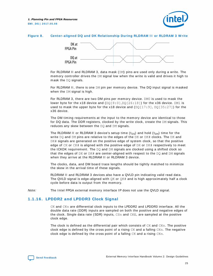
Figure 8. Center-aligned DQ and DK Relationship During RLDRAM II or RLDRAM 3 Write
DK atFPGA Pin
DQ atFPGA Pin
For RLDRAM II and RLDRAM 3, data mask (DM) pins are used only during a write. Thememory controller drives the DM signal low when the write is valid and drives it high tomask the DQ signals.
For RLDRAM II, there is one DM pin per memory device. The DQ input signal is maskedwhen the DM signal is high.
For RLDRAM 3, there are two DM pins per memory device. DM0 is used to mask thelower byte for the x18 device and (DQ[8:0],DQ[26:18]) for the x36 device. DM1 isused to mask the upper byte for the x18 device and (DQ[17:9], DQ[35:27]) for thex36 device.
The DM timing requirements at the input to the memory device are identical to thosefor DQ data. The DDR registers, clocked by the write clock, create the DM signals. Thisreduces any skew between the DQ and DM signals.
The RLDRAM II or RLDRAM 3 device's setup time (tDS) and hold (tDH) time for thewrite DQ and DM pins are relative to the edges of the DK or DK# clocks. The DK andDK# signals are generated on the positive edge of system clock, so that the positiveedge of CK or CK# is aligned with the positive edge of DK or DK# respectively to meetthe tCKDK requirement. The DQ and DM signals are clocked using a shifted clock sothat the edges of DK or DK# are center-aligned with respect to the DQ and DM signalswhen they arrive at the RLDRAM II or RLDRAM 3 device.
The clocks, data, and DM board trace lengths should be tightly matched to minimizethe skew in the arrival time of these signals.
RLDRAM II and RLDRAM 3 devices also have a QVLD pin indicating valid read data.The QVLD signal is edge-aligned with QK or QK# and is high approximately half a clockcycle before data is output from the memory.
Note: The Intel FPGA external memory interface IP does not use the QVLD signal.
1.1.16. LPDDR2 and LPDDR3 Clock Signal
CK and CKn are differential clock inputs to the LPDDR2 and LPDDR3 interface. All thedouble data rate (DDR) inputs are sampled on both the positive and negative edges ofthe clock. Single data rate (SDR) inputs, CSn and CKE, are sampled at the positiveclock edge.
The clock is defined as the differential pair which consists of CK and CKn. The positiveclock edge is defined by the cross point of a rising CK and a falling CKn. The negativeclock edge is defined by the cross point of a falling CK and a rising CKn.
1. Planning Pin and FPGA Resources
EMI_DG | 2017.05.08
Send Feedback External Memory Interface Handbook Volume 2: Design Guidelines
25
The SDRAM data sheet specifies timing data for the following:
• tDSH is the DQS falling edge hold time from CK.
• tDSS is the DQS falling edge to the CK setup time.
• tDQSS is the Write command to the first DQS latching transition.
• tDQSCK is the DQS output access time from CK/CKn.
1.1.17. LPDDR2 and LPDDR3 Command and Address Signal
All LPDDR2 and LPDDR3 devices use double data rate architecture on the command/address bus to reduce the number of input pins in the system. The 10-bit command/address bus contains command, address, and bank/row buffer information. Eachcommand uses one clock cycle, during which command information is transferred onboth the positive and negative edges of the clock.
1.1.18. LPDDR2 and LPDDR3 Data, Data Strobe, and DM Signals
LPDDR2 and LPDDR3 devices use bidirectional and differential data strobes.
Differential DQS operation enables improved system timing due to reduced crosstalkand less simultaneous switching noise on the strobe output drivers. The DQ pins arealso bidirectional. DQS is edge-aligned with the read data and centered with the writedata.
DM is the input mask for the write data signal. Input data is masked when DM issampled high coincident with that input data during a write access.
1.1.19. Maximum Number of Interfaces
The maximum number of interfaces supported for a given memory protocol varies,depending on the FPGA in use.
Unless otherwise noted, the calculation for the maximum number of interfaces isbased on independent interfaces where the address or command pins are not shared.The maximum number of independent interfaces is limited to the number of PLLs eachFPGA device has.
Note: You must share DLLs if the total number of interfaces exceeds the number of DLLsavailable in a specific FPGA device. You may also need to share PLL clock outputsdepending on your clock network usage, refer to PLLs and Clock Networks.
Note: For information about the number of DQ and DQS in other packages, refer to the DQand DQS tables in the relevant device handbook.
For interface information for Arria 10 and Stratix 10 devices, you can consult the EMIFDevice Selector on www.altera.com.
Timing closure depends on device resource and routing utilization. For moreinformation about timing closure, refer to the Area and Timing OptimizationTechniques chapter in the Quartus Prime Handbook.
1. Planning Pin and FPGA Resources
EMI_DG | 2017.05.08
External Memory Interface Handbook Volume 2: Design Guidelines Send Feedback
26
Related Information
• PLLs and Clock Networks on page 71
• Intel Arria 10 Device Handbook
• External Memory Interface Device Selector
• Quartus Prime Handbook
1.1.19.1. Maximum Number of DDR SDRAM Interfaces Supported per FPGA
The following table describes the maximum number of ×8 DDR SDRAM componentsthat can fit in the smallest and biggest devices and pin packages assuming the deviceis blank.
Each interface of size n, where n is a multiple of 8, consists of:
• n DQ pins (including error correction coding (ECC))
• n/8 DM pins
• n/8 DQS pins
• 18 address pins
• 6 command pins (CAS#, RAS#, WE#, CKE, and CS#)
• 1 CK, CK# pin pair for up to every three ×8 DDR SDRAM components
Table 5. Maximum Number of DDR SDRAM Interfaces Supported per FPGA
Device Device Type Package Pin Count Maximum Number of Interfaces
Arria II GX EP2AGX190EP2AGX260
1,152 Four ×8 interfaces or one ×72 interface oneach side (no DQ pins on left side)
EP2AGX45EP2AGX65
358 • On top side, one ×16 interface• On bottom side, one ×16 interface• On right side (no DQ pins on left side),
one ×8 interface
Arria II GZ EP2AGZ300EP2AGZ350EP2AGZ225
1,517 Four ×8 interfaces or one ×72 interface oneach side
EP2AGZ300EP2AGZ350
780 • On top side, three ×8 interfaces or one×64 interface
• On bottom side, three ×8 interfaces orone ×64 interface
• No DQ pins on the left and right sides
Stratix III EP3SL340 1,760 • Two ×72 interfaces on both top andbottom sides
• One ×72 interface on both right and leftsides
EP3SE50 484 • Two ×8 interfaces on both top andbottom sides
• Three ×8 interface on both right and leftsides
Stratix IV EP4SGX290EP4SGX360EP4SGX530
1,932 • One ×72 interface on each side
continued...
1. Planning Pin and FPGA Resources
EMI_DG | 2017.05.08
Send Feedback External Memory Interface Handbook Volume 2: Design Guidelines
27
Device Device Type Package Pin Count Maximum Number of Interfaces
or• One ×72 interface on each side and two
additional ×72 wraparound interfaces,only if sharing DLL and PLL resources
EP4SE530EP4SE820
1,760
EP4SGX70EP4SGX110EP4SGX180EP4SGX230
780 • Three ×8 interfaces or one ×64interface on both top and bottom sides
• On left side, one ×48 interface or two×8 interfaces
• No DQ pins on the right side
Related Information
External Memory Interface Device Selector
1.1.19.2. Maximum Number of DDR2 SDRAM Interfaces Supported per FPGA
The following table lists the maximum number of ×8 DDR2 SDRAM components thatcan be fitted in the smallest and biggest devices and pin packages assuming thedevice is blank.
Each interface of size n, where n is a multiple of 8, consists of:
• n DQ pins (including ECC)
• n/8 DM pins
• n/8 DQS, DQSn pin pairs
• 18 address pins
• 7 command pins (CAS#, RAS#, WE#, CKE, ODT, and CS#)
• 1 CK, CK# pin pair up to every three ×8 DDR2 components
Table 6. Maximum Number of DDR2 SDRAM Interfaces Supported per FPGA
Device Device Type Package Pin Count Maximum Number of Interfaces
Arria II GX EP2AGX190EP2AGX260
1,152 Four ×8 interfaces or one ×72 interfaceon each side (no DQ pins on left side)
EP2AGX45EP2AGX65
358 • One ×16 interface on both top andbottom sides
• On right side (no DQ pins on leftside), one ×8 interface
Arria II GZ EP2AGZ300EP2AGZ350EP2AGZ225
1,517 Four ×8 interfaces or one ×72 interfaceon each side
EP2AGZ300EP2AGZ350
780 • Three ×8 interfaces or one ×64interface on both top and bottomsides
• No DQ pins on the left and right sides
Arria V 5AGXB15AGXB35AGXB55AGXB75AGTD35AGTD7
1,517 • Two ×72 interfaces on both top andbottom sides
• No DQ pins on left and right sides
continued...
1. Planning Pin and FPGA Resources
EMI_DG | 2017.05.08
External Memory Interface Handbook Volume 2: Design Guidelines Send Feedback
28
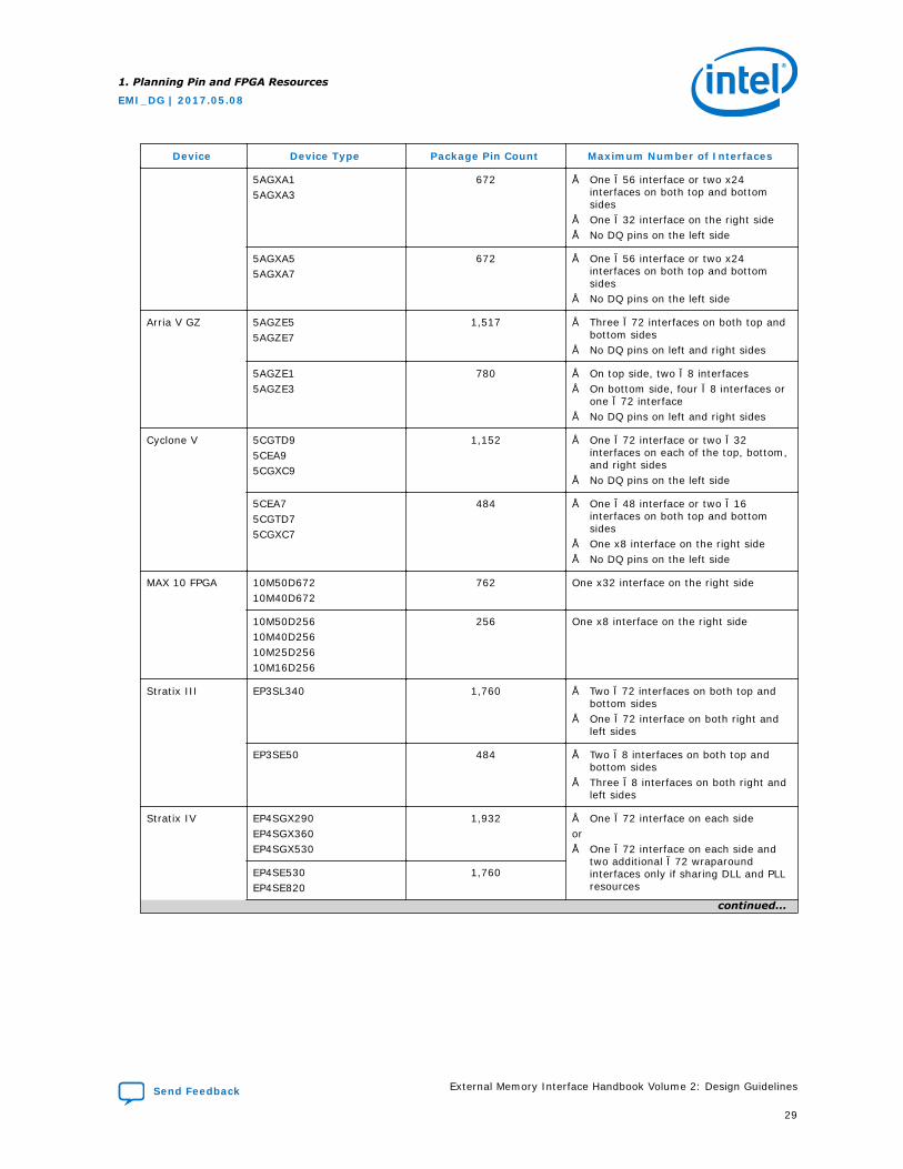
Device Device Type Package Pin Count Maximum Number of Interfaces
5AGXA15AGXA3
672 • One ×56 interface or two x24interfaces on both top and bottomsides
• One ×32 interface on the right side• No DQ pins on the left side
5AGXA55AGXA7
672 • One ×56 interface or two x24interfaces on both top and bottomsides
• No DQ pins on the left side
Arria V GZ 5AGZE55AGZE7
1,517 • Three ×72 interfaces on both top andbottom sides
• No DQ pins on left and right sides
5AGZE15AGZE3
780 • On top side, two ×8 interfaces• On bottom side, four ×8 interfaces or
one ×72 interface• No DQ pins on left and right sides
Cyclone V 5CGTD95CEA95CGXC9
1,152 • One ×72 interface or two ×32interfaces on each of the top, bottom,and right sides
• No DQ pins on the left side
5CEA75CGTD75CGXC7
484 • One ×48 interface or two ×16interfaces on both top and bottomsides
• One x8 interface on the right side• No DQ pins on the left side
MAX 10 FPGA 10M50D67210M40D672
762 One x32 interface on the right side
10M50D25610M40D25610M25D25610M16D256
256 One x8 interface on the right side
Stratix III EP3SL340 1,760 • Two ×72 interfaces on both top andbottom sides
• One ×72 interface on both right andleft sides
EP3SE50 484 • Two ×8 interfaces on both top andbottom sides
• Three ×8 interfaces on both right andleft sides
Stratix IV EP4SGX290EP4SGX360EP4SGX530
1,932 • One ×72 interface on each sideor• One ×72 interface on each side and
two additional ×72 wraparoundinterfaces only if sharing DLL and PLLresources
EP4SE530EP4SE820
1,760
continued...
1. Planning Pin and FPGA Resources
EMI_DG | 2017.05.08
Send Feedback External Memory Interface Handbook Volume 2: Design Guidelines
29
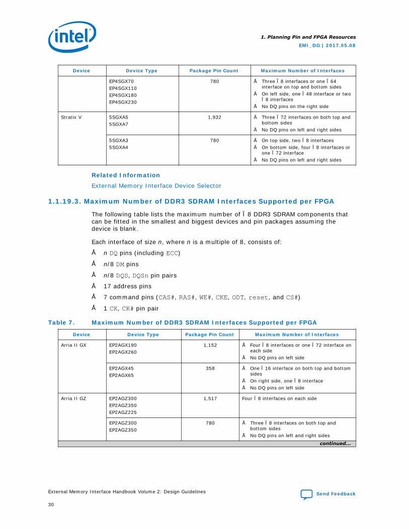
Device Device Type Package Pin Count Maximum Number of Interfaces
EP4SGX70EP4SGX110EP4SGX180EP4SGX230
780 • Three ×8 interfaces or one ×64interface on top and bottom sides
• On left side, one ×48 interface or two×8 interfaces
• No DQ pins on the right side
Stratix V 5SGXA55SGXA7
1,932 • Three ×72 interfaces on both top andbottom sides
• No DQ pins on left and right sides
5SGXA35SGXA4
780 • On top side, two ×8 interfaces• On bottom side, four ×8 interfaces or
one ×72 interface• No DQ pins on left and right sides
Related Information
External Memory Interface Device Selector
1.1.19.3. Maximum Number of DDR3 SDRAM Interfaces Supported per FPGA
The following table lists the maximum number of ×8 DDR3 SDRAM components thatcan be fitted in the smallest and biggest devices and pin packages assuming thedevice is blank.
Each interface of size n, where n is a multiple of 8, consists of:
• n DQ pins (including ECC)
• n/8 DM pins
• n/8 DQS, DQSn pin pairs
• 17 address pins
• 7 command pins (CAS#, RAS#, WE#, CKE, ODT, reset, and CS#)
• 1 CK, CK# pin pair
Table 7. Maximum Number of DDR3 SDRAM Interfaces Supported per FPGA
Device Device Type Package Pin Count Maximum Number of Interfaces
Arria II GX EP2AGX190EP2AGX260
1,152 • Four ×8 interfaces or one ×72 interface oneach side
• No DQ pins on left side
EP2AGX45EP2AGX65
358 • One ×16 interface on both top and bottomsides
• On right side, one ×8 interface• No DQ pins on left side
Arria II GZ EP2AGZ300EP2AGZ350EP2AGZ225
1,517 Four ×8 interfaces on each side
EP2AGZ300EP2AGZ350
780 • Three ×8 interfaces on both top andbottom sides
• No DQ pins on left and right sides
continued...
1. Planning Pin and FPGA Resources
EMI_DG | 2017.05.08
External Memory Interface Handbook Volume 2: Design Guidelines Send Feedback
30
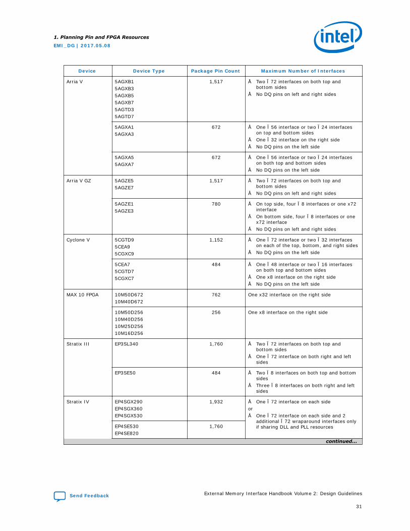
Device Device Type Package Pin Count Maximum Number of Interfaces
Arria V 5AGXB15AGXB35AGXB55AGXB75AGTD35AGTD7
1,517 • Two ×72 interfaces on both top andbottom sides
• No DQ pins on left and right sides
5AGXA15AGXA3
672 • One ×56 interface or two ×24 interfaceson top and bottom sides
• One ×32 interface on the right side• No DQ pins on the left side
5AGXA55AGXA7
672 • One ×56 interface or two ×24 interfaceson both top and bottom sides
• No DQ pins on the left side
Arria V GZ 5AGZE55AGZE7
1,517 • Two ×72 interfaces on both top andbottom sides
• No DQ pins on left and right sides
5AGZE15AGZE3
780 • On top side, four ×8 interfaces or one x72interface
• On bottom side, four ×8 interfaces or onex72 interface
• No DQ pins on left and right sides
Cyclone V 5CGTD95CEA95CGXC9
1,152 • One ×72 interface or two ×32 interfaceson each of the top, bottom, and right sides
• No DQ pins on the left side
5CEA75CGTD75CGXC7
484 • One ×48 interface or two ×16 interfaceson both top and bottom sides
• One x8 interface on the right side• No DQ pins on the left side
MAX 10 FPGA 10M50D67210M40D672
762 One x32 interface on the right side
10M50D25610M40D25610M25D25610M16D256
256 One x8 interface on the right side
Stratix III EP3SL340 1,760 • Two ×72 interfaces on both top andbottom sides
• One ×72 interface on both right and leftsides
EP3SE50 484 • Two ×8 interfaces on both top and bottomsides
• Three ×8 interfaces on both right and leftsides
Stratix IV EP4SGX290EP4SGX360EP4SGX530
1,932 • One ×72 interface on each sideor• One ×72 interface on each side and 2
additional ×72 wraparound interfaces onlyif sharing DLL and PLL resourcesEP4SE530
EP4SE8201,760
continued...
1. Planning Pin and FPGA Resources
EMI_DG | 2017.05.08
Send Feedback External Memory Interface Handbook Volume 2: Design Guidelines
31
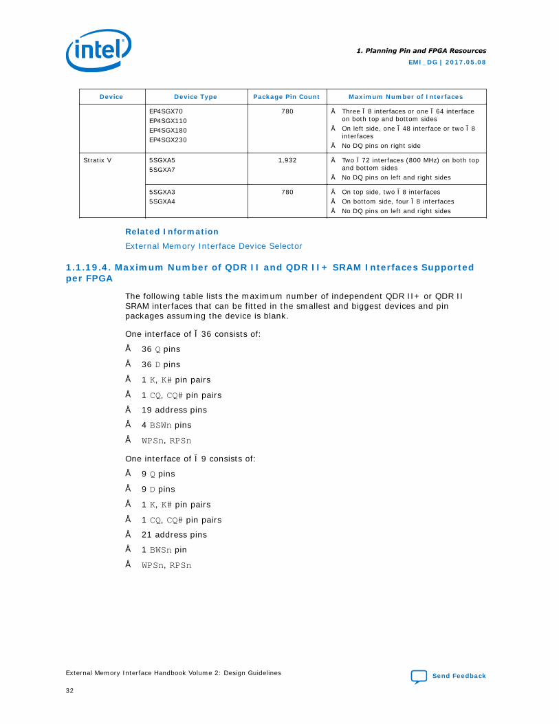
Device Device Type Package Pin Count Maximum Number of Interfaces
EP4SGX70EP4SGX110EP4SGX180EP4SGX230
780 • Three ×8 interfaces or one ×64 interfaceon both top and bottom sides
• On left side, one ×48 interface or two ×8interfaces
• No DQ pins on right side
Stratix V 5SGXA55SGXA7
1,932 • Two ×72 interfaces (800 MHz) on both topand bottom sides
• No DQ pins on left and right sides
5SGXA35SGXA4
780 • On top side, two ×8 interfaces• On bottom side, four ×8 interfaces• No DQ pins on left and right sides
Related Information
External Memory Interface Device Selector
1.1.19.4. Maximum Number of QDR II and QDR II+ SRAM Interfaces Supportedper FPGA
The following table lists the maximum number of independent QDR II+ or QDR IISRAM interfaces that can be fitted in the smallest and biggest devices and pinpackages assuming the device is blank.
One interface of ×36 consists of:
• 36 Q pins
• 36 D pins
• 1 K, K# pin pairs
• 1 CQ, CQ# pin pairs
• 19 address pins
• 4 BSWn pins
• WPSn, RPSn
One interface of ×9 consists of:
• 9 Q pins
• 9 D pins
• 1 K, K# pin pairs
• 1 CQ, CQ# pin pairs
• 21 address pins
• 1 BWSn pin
• WPSn, RPSn
1. Planning Pin and FPGA Resources
EMI_DG | 2017.05.08
External Memory Interface Handbook Volume 2: Design Guidelines Send Feedback
32
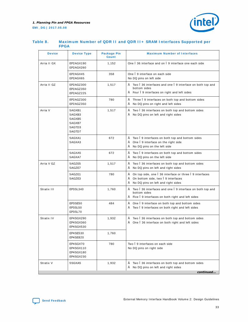
Table 8. Maximum Number of QDR II and QDR II+ SRAM Interfaces Supported perFPGA
Device Device Type Package PinCount
Maximum Number of Interfaces
Arria II GX EP2AGX190EP2AGX260
1,152 One ×36 interface and on ×9 interface one each side
EP2AGX45EP2AGX65
358 One ×9 interface on each sideNo DQ pins on left side
Arria II GZ EP2AGZ300EP2AGZ350EP2AGZ225
1,517 • Two ×36 interfaces and one ×9 interface on both top andbottom sides
• Four ×9 interfaces on right and left sides
EP2AGZ300EP2AGZ350
780 • Three ×9 interfaces on both top and bottom sides• No DQ pins on right and left sides
Arria V 5AGXB15AGXB35AGXB55AGXB75AGTD35AGTD7
1,517 • Two ×36 interfaces on both top and bottom sides• No DQ pins on left and right sides
5AGXA15AGXA3
672 • Two ×9 interfaces on both top and bottom sides• One ×9 interface on the right side• No DQ pins on the left side
5AGXA55AGXA7
672 • Two ×9 interfaces on both top and bottom sides• No DQ pins on the left side
Arria V GZ 5AGZE55AGZE7
1,517 • Two ×36 interfaces on both top and bottom sides• No DQ pins on left and right sides
5AGZE15AGZE3
780 • On top side, one ×36 interface or three ×9 interfaces• On bottom side, two ×9 interfaces• No DQ pins on left and right sides
Stratix III EP3SL340 1,760 • Two ×36 interfaces and one ×9 interface on both top andbottom sides
• Five ×9 interfaces on both right and left sides
EP3SE50EP3SL50EP3SL70
484 • One ×9 interface on both top and bottom sides• Two ×9 interfaces on both right and left sides
Stratix IV EP4SGX290EP4SGX360EP4SGX530
1,932 • Two ×36 interfaces on both top and bottom sides• One ×36 interface on both right and left sides
EP4SE530EP4SE820
1,760
EP4SGX70EP4SGX110EP4SGX180EP4SGX230
780 Two ×9 interfaces on each sideNo DQ pins on right side
Stratix V 5SGXA5 1,932 • Two ×36 interfaces on both top and bottom sides• No DQ pins on left and right sides
continued...
1. Planning Pin and FPGA Resources
EMI_DG | 2017.05.08
Send Feedback External Memory Interface Handbook Volume 2: Design Guidelines
33
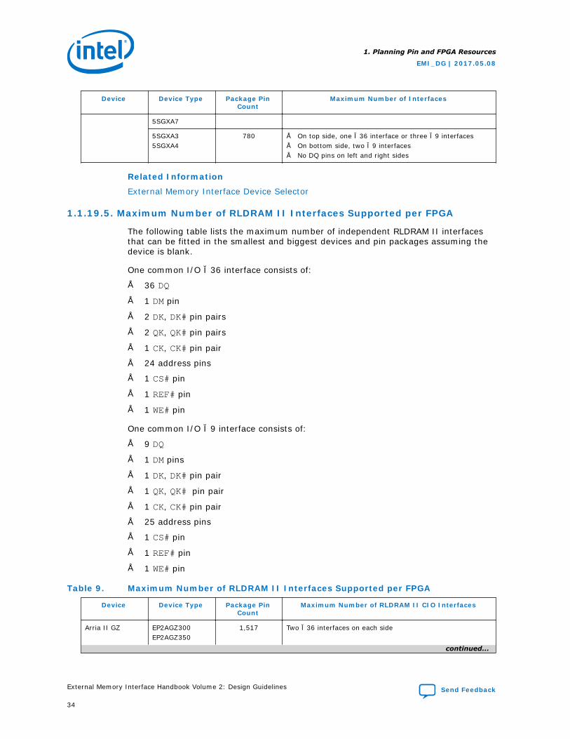
Device Device Type Package PinCount
Maximum Number of Interfaces
5SGXA7
5SGXA35SGXA4
780 • On top side, one ×36 interface or three ×9 interfaces• On bottom side, two ×9 interfaces• No DQ pins on left and right sides
Related Information
External Memory Interface Device Selector
1.1.19.5. Maximum Number of RLDRAM II Interfaces Supported per FPGA
The following table lists the maximum number of independent RLDRAM II interfacesthat can be fitted in the smallest and biggest devices and pin packages assuming thedevice is blank.
One common I/O ×36 interface consists of:
• 36 DQ
• 1 DM pin
• 2 DK, DK# pin pairs
• 2 QK, QK# pin pairs
• 1 CK, CK# pin pair
• 24 address pins
• 1 CS# pin
• 1 REF# pin
• 1 WE# pin
One common I/O ×9 interface consists of:
• 9 DQ
• 1 DM pins
• 1 DK, DK# pin pair
• 1 QK, QK# pin pair
• 1 CK, CK# pin pair
• 25 address pins
• 1 CS# pin
• 1 REF# pin
• 1 WE# pin
Table 9. Maximum Number of RLDRAM II Interfaces Supported per FPGA
Device Device Type Package PinCount
Maximum Number of RLDRAM II CIO Interfaces
Arria II GZ EP2AGZ300EP2AGZ350
1,517 Two ×36 interfaces on each side
continued...
1. Planning Pin and FPGA Resources
EMI_DG | 2017.05.08
External Memory Interface Handbook Volume 2: Design Guidelines Send Feedback
34
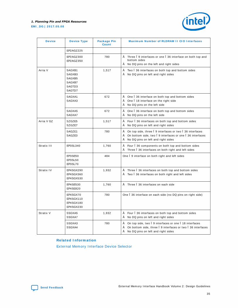
Device Device Type Package PinCount
Maximum Number of RLDRAM II CIO Interfaces
EP2AGZ225
EP2AGZ300EP2AGZ350
780 • Three ×9 interfaces or one ×36 interface on both top andbottom sides
• No DQ pins on the left and right sides
Arria V 5AGXB15AGXB35AGXB55AGXB75AGTD35AGTD7
1,517 • Two ×36 interfaces on both top and bottom sides• No DQ pins on left and right sides
5AGXA15AGXA3
672 • One ×36 interface on both top and bottom sides• One ×18 interface on the right side• No DQ pins on the left side
5AGXA55AGXA7
672 • One ×36 interface on both top and bottom sides• No DQ pins on the left side
Arria V GZ 5ZGZE55ZGZE7
1,517 • Four ×36 interfaces on both top and bottom sides• No DQ pins on left and right sides
5AGZE15AGZE3
780 • On top side, three ×9 interfaces or two ×36 interfaces• On bottom side, two ×9 interfaces or one ×36 interfaces• No DQ pins on left and right sides
Stratix III EP3SL340 1,760 • Four ×36 components on both top and bottom sides• Three ×36 interfaces on both right and left sides
EP3SE50EP3SL50EP3SL70
484 One ×9 interface on both right and left sides
Stratix IV EP4SGX290EP4SGX360EP4SGX530
1,932 • Three ×36 interfaces on both top and bottom sides• Two ×36 interfaces on both right and left sides
EP4SE530EP4SE820
1,760 • Three ×36 interfaces on each side
EP4SGX70EP4SGX110EP4SGX180EP4SGX230
780 One ×36 interface on each side (no DQ pins on right side)
Stratix V 5SGXA55SGXA7
1,932 • Four ×36 interfaces on both top and bottom sides• No DQ pins on left and right sides
5SGXA35SGXA4
780 • On top side, two ×9 interfaces or one ×18 interfaces• On bottom side, three ×9 interfaces or two ×36 interfaces• No DQ pins on left and right sides
Related Information
External Memory Interface Device Selector
1. Planning Pin and FPGA Resources
EMI_DG | 2017.05.08
Send Feedback External Memory Interface Handbook Volume 2: Design Guidelines
35
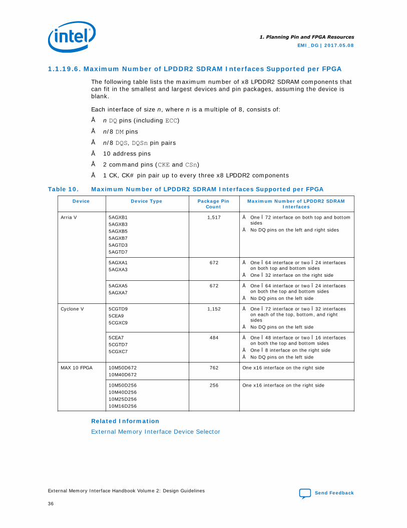
1.1.19.6. Maximum Number of LPDDR2 SDRAM Interfaces Supported per FPGA
The following table lists the maximum number of x8 LPDDR2 SDRAM components thatcan fit in the smallest and largest devices and pin packages, assuming the device isblank.
Each interface of size n, where n is a multiple of 8, consists of:
• n DQ pins (including ECC)
• n/8 DM pins
• n/8 DQS, DQSn pin pairs
• 10 address pins
• 2 command pins (CKE and CSn)
• 1 CK, CK# pin pair up to every three x8 LPDDR2 components
Table 10. Maximum Number of LPDDR2 SDRAM Interfaces Supported per FPGA
Device Device Type Package PinCount
Maximum Number of LPDDR2 SDRAMInterfaces
Arria V 5AGXB15AGXB35AGXB55AGXB75AGTD35AGTD7
1,517 • One ×72 interface on both top and bottomsides
• No DQ pins on the left and right sides
5AGXA15AGXA3
672 • One ×64 interface or two ×24 interfaceson both top and bottom sides
• One ×32 interface on the right side
5AGXA55AGXA7
672 • One ×64 interface or two ×24 interfaceson both the top and bottom sides
• No DQ pins on the left side
Cyclone V 5CGTD95CEA95CGXC9
1,152 • One ×72 interface or two ×32 interfaceson each of the top, bottom, and rightsides
• No DQ pins on the left side
5CEA75CGTD75CGXC7
484 • One ×48 interface or two ×16 interfaceson both the top and bottom sides
• One ×8 interface on the right side• No DQ pins on the left side
MAX 10 FPGA 10M50D67210M40D672
762 One x16 interface on the right side
10M50D25610M40D25610M25D25610M16D256
256 One x16 interface on the right side
Related Information
External Memory Interface Device Selector
1. Planning Pin and FPGA Resources
EMI_DG | 2017.05.08
External Memory Interface Handbook Volume 2: Design Guidelines Send Feedback
36
1.1.20. OCT Support
If the memory interface uses any FPGA OCT calibrated series, parallel, or dynamictermination for any I/O in your design, you need a calibration block for the OCTcircuitry. This calibration block is not required to be within the same bank or side ofthe device as the memory interface pins. However, the block requires a pair of RUP andRDN or RZQ pins that must be placed within an I/O bank that has the same VCCIOvoltage as the VCCIO voltage of the I/O pins that use the OCT calibration block.
The RZQ pin in Arria 10, Stratix 10, Arria V, Stratix V, and Cyclone V devices can beused as a general purpose I/O pin when it is not used to support OCT, provided thesignal conforms to the bank voltage requirements.
The RUP and RDN pins in Arria II GX, Arria II GZ, MAX 10, Stratix III, and Stratix IVdevices are dual functional pins that can also be used as DQ and DQS pins in whenthey are not used to support OCT, giving the following impacts on your DQS groups:
• If the RUP and RDN pins are part of a ×4 DQS group, you cannot use that DQSgroup in ×4 mode.
• If the RUP and RDN pins are part of a ×8 DQS group, you can only use this group in×8 mode if any of the following conditions apply:
— You are not using DM or BWSn pins.
— You are not using a ×8 or ×9 QDR II SRAM device, as the RUP and RDN pinsmay have dual purpose function as the CQn pins. In this case, pick differentpin locations for RUP and RDN pins, to avoid conflict with memory interface pinplacement. You have the choice of placing the RUP and RDN pins in the samebank as the write data pin group or address and command pin group.
— You are not using complementary or differential DQS pins.
Note: The Altera external memory interface IP does not support ×8 QDR II SRAM devices inthe Quartus Prime software.
A DQS/DQ ×8/×9 group in Arria II GZ, Stratix III, and Stratix IV devices comprises 12pins. A typical ×8 memory interface consists of one DQS, one DM, and eight DQ pinswhich add up to 10 pins. If you choose your pin assignment carefully, you can use thetwo extra pins for RUP and RDN. However, if you are using differential DQS, you do nothave enough pins for RUP and RDN as you only have one pin leftover. In this case, asyou do not have to put the OCT calibration block with the DQS or DQ pins, you can pickdifferent locations for the RUP and RDN pins. As an example, you can place it in the I/Obank that contains the address and command pins, as this I/O bank has the sameVCCIO voltage as the I/O bank containing the DQS and DQ pins.
There is no restriction when using ×16/×18 or ×32/×36 DQS groups that include the×4 groups when pin members are used as RUP and RDN pins, as there are enough extrapins that can be used as DQS or DQ pins.
You must pick your DQS and DQ pins manually for the ×8, ×9, ×16 and ×18, or ×32and ×36 groups, if they are using RUP and RDN pins within the group. The QuartusPrime software might not place these pins optimally and might be unable to fit thedesign.
1. Planning Pin and FPGA Resources
EMI_DG | 2017.05.08
Send Feedback External Memory Interface Handbook Volume 2: Design Guidelines
37
1.2. Guidelines for Intel Arria® 10 External Memory Interface IP
The Intel Arria® 10 device contains up to two I/O columns that can be used byexternal memory interfaces. The Arria 10 I/O subsystem resides in the I/O columns.Each column contains multiple I/O banks, each of which consists of four I/O lanes. AnI/O lane is a group of twelve I/O ports.
The I/O column, I/O bank, I/O lane, adjacent I/O bank, and pairing pin for everyphysical I/O pin can be uniquely identified using the Bank Number and Indexwithin I/O Bank values which are defined in each Arria 10 device pin-out file.
• The numeric component of the Bank Number value identifies the I/O column,while the letter represents the I/O bank.
• The Index within I/O Bank value falls within one of the following ranges: 0 to11, 12 to 23, 24 to 35, or 36 to 47, and represents I/O lanes 1, 2, 3, and 4,respectively.
• The adjacent I/O bank is defined as the I/O bank with same column number butthe letter is either before or after the respective I/O bank letter in the A-Z system.
• The pairing pin for an I/O pin is located in the same I/O bank. You can identify thepairing pin by adding one to its Index within I/O Bank number (if it is aneven number), or by subtracting one from its Index within I/O Bank number(if it is an odd number).
For example, a physical pin with a Bank Number of 2K and Index within I/OBank of 22, indicates that the pin resides in I/O lane 2, in I/O bank 2K, in column 2.The adjacent I/O banks are 2J and 2L. The pairing pin for this physical pin is the pinwith an Index within I/O Bank of 23 and Bank Number of 2K.
Related Information
Restrictions on I/O Bank Usage for Arria 10 EMIF IP with HPS
1.2.1. General Pin-Out Guidelines for Arria 10 EMIF IP
You should follow the recommended guidelines when performing pin placement for allexternal memory interface pins targeting Arria 10 devices, whether you are using theAltera hard memory controller or your own solution.
If you are using the Altera hard memory controller, you should employ the relative pinlocations defined in the <variation_name>/altera_emif_arch_nf_versionnumber/<synth|sim>/<variation_name>_altera_emif_arch_nf_versionnumber_<unique ID>_readme.txt file, which is generated with your IP.
Note: 1. EMIF IP pin-out requirements for the Arria 10 Hard Processor Subsystem (HPS)are more restrictive than for a non-HPS memory interface. The HPS EMIF IPdefines a fixed pin-out in the Quartus Prime IP file (.qip), based on the IPconfiguration. When targeting Arria 10 HPS, you do not need to make locationassignments for external memory interface pins. To obtain the HPS-specificexternal memory interface pin-out, compile the interface in the Quartus Primesoftware. Alternatively, consult the device handbook or the device pin-out files.For information on how you can customize the HPS EMIF pin-out, refer toRestrictions on I/O Bank Usage for Arria 10 EMIF IP with HPS.
2. Ping Pong PHY, PHY only, RLDRAMx , QDRx and LPDDR3 are not supported withHPS.
1. Planning Pin and FPGA Resources
EMI_DG | 2017.05.08
External Memory Interface Handbook Volume 2: Design Guidelines Send Feedback
38
Observe the following general guidelines for placing pins for your Arria 10 externalmemory interface:
1. Ensure that the pins of a single external memory interface reside within a singleI/O column.
2. An external memory interface can occupy one or more banks in the same I/Ocolumn. When an interface must occupy multiple banks, ensure that those banksare adjacent to one another.
3. Be aware that any pin in the same bank that is not used by an external memoryinterface is available for use as a general purpose I/O of compatible voltage andtermination settings.
4. All address and command pins and their associated clock pins (CK and CK#) mustreside within a single bank. The bank containing the address and command pins isidentified as the address and command bank.
5. To minimize latency, when the interface uses more than two banks, you mustselect the center bank of the interface as the address and command bank.
6. The address and command pins and their associated clock pins in the address andcommand bank must follow a fixed pin-out scheme, as defined in the Arria 10External Memory Interface Pin Information File, which is available onwww.altera.com.
You do not have to place every address and command pin manually. If you assignthe location for one address and command pin, the Fitter automatically places theremaining address and command pins.
Note: The pin-out scheme is a hardware requirement that you must follow, andcan vary according to the topology of the memory device. Some schemesrequire three lanes to implement address and command pins, while othersrequire four lanes. To determine which scheme to follow, refer to themessages window during parameterization of your IP, or to the<variation_name>/altera_emif_arch_nf_<version>/<synth|sim>/<variation_name>_altera_emif_arch_nf_<version>_<uniqueID>_readme.txt file after you have generated your IP.
7. An unused I/O lane in the address and command bank can serve to implement adata group, such as a x8 DQS group. The data group must be from the samecontroller as the address and command signals.
8. An I/O lane must not be used by both address and command pins and data pins.
9. Place read data groups according to the DQS grouping in the pin table and pinplanner. Read data strobes (such as DQS and DQS#) or read clocks (such as CQand CQ# / QK and QK#) must reside at physical pins capable of functioning asDQS/CQ and DQSn/CQn for a specific read data group size. You must place theassociated read data pins (such as DQ and Q), within the same group.
1. Planning Pin and FPGA Resources
EMI_DG | 2017.05.08
Send Feedback External Memory Interface Handbook Volume 2: Design Guidelines
39

Note: a. Unlike other device families, there is no need to swap CQ/CQ# pins incertain QDR II and QDR II+ latency configurations.
b. QDR-IV requires that the polarity of all QKB/QKB# pins be swapped withrespect to the polarity of the differential buffer inputs on the FPGA toensure correct data capture on port B. All QKB pins on the memorydevice must be connected to the negative pins of the input buffers onthe FPGA side, and all QKB# pins on the memory device must beconnected to the positive pins of the input buffers on the FPGA side.Notice that the port names at the top-level of the IP already reflect thisswap (that is, mem_qkb is assigned to the negative buffer leg, andmem_qkb_n is assigned to the positive buffer leg).
10. You can use a single I/O lane to implement two x4 DQS groups. The pin tablespecifies which pins within an I/O lane can be used for the two pairs of DQS andDQS# signals. In addition, for x4 DQS groups you must observe the followingrules:
• There must be an even number of x4 groups in an external memory interface.
• DQS group 0 and DQS group 1 must be placed in the same I/O lane. Similarly,DQS group 2 and group 3 must be in the same I/O lane. Generally, DQS groupX and DQS group X+1 must be in the same I/O lane, where X is an evennumber.
11. You should place the write data groups according to the DQS grouping in the pintable and pin planner. Output-only data clocks for QDR II, QDR II+, and QDR II+Extreme, and RLDRAM 3 protocols need not be placed on DQS/DQSn pins, butmust be placed on a differential pin pair. They must be placed in the same I/Obank as the corresponding DQS group.
Note: For RLDRAM 3, x36 device, DQ[8:0] and DQ[26:18] are referenced toDK0/DK0#, and DQ[17:9] and DQ[35:27] are referenced to DK1/DK1#.
12. For protocols and topologies with bidirectional data pins where a write data groupconsists of multiple read data groups, you should place the data groups and theirrespective write and read clock in the same bank to improve I/O timing.
You do not need to specify the location of every data pin manually. If you assignthe location for the read capture strobe/clock pin pairs, the Fitter willautomatically place the remaining data pins.
13. Ensure that DM/BWS pins are paired with a write data pin by placing one in an I/Opin and another in the pairing pin for that I/O pin. It is recommended—though notrequired—that you follow the same rule for DBI pins, so that at a later date youhave the freedom to repurpose the pin as DM.
Note: 1. x4 mode does not support DM/DBI, or Arria 10 EMIF IP for HPS.
2. If you are using an Arria 10 EMIF IP-based RLDRAM II or RLDRAM 3 externalmemory interface, you should ensure that all the pins in a DQS group (that is, DQ,DM, DK, and QK) are placed in the same I/O bank. This requirement facilitatestiming closure and is necessary for successful compilation of your design.
Multiple Interfaces in the Same I/O Column
To place multiple interfaces in the same I/O column, you must ensure that the globalreset signals (global_reset_n) for each individual interface all come from the sameinput pin or signal.
1. Planning Pin and FPGA Resources
EMI_DG | 2017.05.08
External Memory Interface Handbook Volume 2: Design Guidelines Send Feedback
40
I/O Banks Selection
• For each memory interface, select consecutive I/O banks.
• A memory interface can only span across I/O banks in the same I/O column.
• Because I/O bank 2A is also employed for configuration-related operations, youcan use it to construct external memory interfaces only when the followingconditions are met:
— The pins required for configuration related use (such as configuration bus forFast Passive Parallel mode or control signals for Partial Reconfiguration) arenever shared with pins selected for EMIF use, even after configuration iscomplete.
— The I/O voltages are compatible.
— The design has achieved a successful fit in the Quartus Prime software.
Refer to the Arria 10 Device Handbook and the Configuration Function column ofthe Pin-Out files for more information about pins and configuration modes.
• The number of I/O banks that you require depends on the memory interfacewidth.
• The 3V I/O bank does not support dynamic OCT or calibrated OCT. To place amemory interface in a 3V I/O bank, ensure that calibrated OCT is disabled for theaddress/command signals, the memory clock signals, and the data bus signals,during IP generation.
• In some device packages, the number of I/O pins in some LVDS I/O banks is lessthat 48 pins.
Address/Command Pins Location
• All address/command pins for a controller must be in a single I/O bank.
• If your interface uses multiple I/O banks, the address/command pins must use themiddle bank. If the number of banks used by the interface is even, any of the twomiddle I/O banks can be used for address/command pins.
• Address/command pins and data pins cannot share an I/O lane but can share anI/O bank.
• The address/command pin locations for the soft and hard memory controllers arepredefined. In the External Memory Interface Pin Information for Devicesspreadsheet, each index in the "Index within I/O bank" column denotes adedicated address/command pin function for a given protocol. The index numberof the pin specifies to which I/O lane the pin belongs:
— I/O lane 0—Pins with index 0 to 11
— I/O lane 1—Pins with index 12 to 23
— I/O lane 2—Pins with index 24 to 35
— I/O lane 3—Pins with index 36 to 47
• For memory topologies and protocols that require only three I/O lanes for theaddress/command pins, use I/O lanes 0, 1, and 2.
• Unused address/command pins in an I/O lane can be used as general-purpose I/Opins.
1. Planning Pin and FPGA Resources
EMI_DG | 2017.05.08
Send Feedback External Memory Interface Handbook Volume 2: Design Guidelines
41
CK Pins Assignment
Assign the clock pin (CK pin) according to the number of I/O banks in an interface:
• The number of I/O banks is odd—assign one CK pin to the middle I/O bank.
• The number of I/O banks is even—assign the CK pin to any one of the middle twoI/O banks.
Although the Fitter can automatically select the required I/O banks, Intel recommendsthat you make the selection manually to reduce the pre-fit run time.
PLL Reference Clock Pin Placement
Place the PLL reference clock pin in the address/command bank. Other I/O banks maynot have free pins that you can use as the PLL reference clock pin:
• If you are sharing the PLL reference clock pin between several interfaces, the I/Obanks must be consecutive.
The Arria 10 External Memory Interface IP does not support PLL cascading.
RZQ Pin Placement
You may place the RZQ pin in any I/O bank in an I/O column with the correct VCCIOand VCCPT for the memory interface I/O standard in use. The recommended locationis in the address/command I/O bank.
DQ and DQS Pins Assignment
Intel recommends that you assign the DQS pins to the remaining I/O lanes in the I/Obanks as required:
• Constrain the DQ and DQS signals of the same DQS group to the same I/O lane.
• DQ signals from two different DQS groups cannot be constrained to the same I/Olane.
If you do not specify the DQS pins assignment, the Fitter will automatically select theDQS pins.
Sharing an I/O Bank Across Multiple Interfaces
If you are sharing an I/O bank across multiple external memory interfaces, followthese guidelines:
• The interfaces must use the same protocol, voltage, data rate, frequency, and PLLreference clock.
• You cannot use an I/O bank as the address/command bank for more than oneinterface. The memory controller and sequencer cannot be shared.
• You cannot share an I/O lane. There is only one DQS input per I/O lane, and anI/O lane can only connect to one memory controller.
Ping Pong PHY Implementation
The Ping Pong PHY feature instantiates two hard memory controllers—one for theprimary interface and one for the secondary interface. The hard memory controller I/Obank of the primary interface is used for address and command and is always adjacent
1. Planning Pin and FPGA Resources
EMI_DG | 2017.05.08
External Memory Interface Handbook Volume 2: Design Guidelines Send Feedback
42
and above the hard memory controller I/O bank of the secondary interface. All fourlanes of the primary hard memory controller I/O bank are used for address andcommand.
When you use Ping Pong PHY, the EMIF IP exposes two independent Avalon-MMinterfaces to user logic; these interfaces correspond to the two hard memorycontrollers inside the interface. Each Avalon-MM interface has its own set of clock andreset signals. Refer to Qsys Interfaces for more information on the additional signalsexposed by Ping Pong PHY interfaces.
For more information on Ping Pong PHY in Arria 10, refer to Functional Description—Arria 10 EMIF, in this handbook. For pin allocation information for Arria 10 devices,refer to External Memory Interface Pin Information for Arria 10 Devices onwww.altera.com.
Additional Requirements for DDR3 and DDR4 Ping-Pong PHY Interfaces
If you are using Ping Pong PHY with a DDR3 or DDR4 external memory interface on anArria 10 device, follow these guidelines:
• The address and command I/O bank must not contain any DQS group.
• I/O banks that are above the address and command I/O bank must contain onlydata pins of the primary interface—that is, the interface with the lower DQS groupindices.
• The I/O bank immediately below the address and command I/O bank must containat least one DQS group of the secondary interface—that is, the interface with thehigher DQS group indices. This I/O bank can, but is not required to, contain DQSgroups of the primary interface.
• I/O banks that are two or more banks below the address and command I/O bankmust contain only data pins of the secondary interface.
Related Information
• Pin-Out Files for Intel FPGAs
• Functional Description—Arria 10 EMIF
• External Memory Interface Pin Information for Arria 10 Devices
• Restrictions on I/O Bank Usage for Arria 10 EMIF IP with HPS
1.2.2. Resource Sharing Guidelines for Arria 10 EMIF IP
In Arria 10, different external memory interfaces can share PLL reference clock pins,core clock networks, I/O banks, and hard Nios processors. Each I/O bank has DLL andPLL resources, therefore these do not need to be shared. The Fitter automaticallymerges DLL and PLL resources when a bank is shared by different external memoryinterfaces, and duplicates them for a multi-I/O-bank external memory interface.
Multiple Interfaces in the Same I/O Column
To place multiple interfaces in the same I/O column, you must ensure that the globalreset signals (global_reset_n) for each individual interface all come from the sameinput pin or signal.
1. Planning Pin and FPGA Resources
EMI_DG | 2017.05.08
Send Feedback External Memory Interface Handbook Volume 2: Design Guidelines
43
PLL Reference Clock Pin
To conserve pin usage and enable core clock network and I/O bank sharing, you canshare a PLL reference clock pin between multiple external memory interfaces. Sharingof a PLL reference clock pin also implies sharing of the reference clock network.
Observe the following guidelines for sharing the PLL reference clock pin:
1. To share a PLL reference clock pin, connect the same signal to the pll_ref_clkport of multiple external memory interfaces in the RTL code.
2. Place related external memory interfaces in the same I/O column.
3. Place related external memory interfaces in adjacent I/O banks. If you leave anunused I/O bank between the I/O banks used by the external memory interfaces,that I/O bank cannot be used by any other external memory interface with adifferent PLL reference clock signal.
Note: The pll_ref_clk pin can be placed in the address and command I/O bank or in adata I/O bank, there is no impact on timing. However, for greatest flexibility duringdebug (such as when creating designs with narrower interfaces), the recommendedplacement is in the address and command I/O bank.
Core Clock Network
To access all external memory interfaces synchronously and to reduce global clocknetwork usage, you may share the same core clock network with other externalmemory interfaces.
Observe the following guidelines for sharing the core clock network:
1. To share a core clock network, connect the clks_sharing_master_out of themaster to the clks_sharing_slave_in of all slaves in the RTL code.
2. Place related external memory interfaces in the same I/O column.
3. Related external memory interface must have the same rate, memory clockfrequency, and PLL reference clock.
4. If you are sharing core clocks between a Ping Pong PHY and a hard controller thathave the same protocol, rate, and frequency, the Ping Pong PHY must be the coreclock master.
I/O Bank
To reduce I/O bank utilization, you may share an I/O Bank with other externalmemory interfaces.
Observe the following guidelines for sharing an I/O Bank:
1. Related external memory interfaces must have the same protocol, rate, memoryclock frequency, and PLL reference clock.
2. You cannot use a given I/O bank as the address and command bank for more thanone external memory interface.
3. You cannot share an I/O lane between external memory interfaces, but an unusedpin can serve as a general purpose I/O pin, of compatible voltage and terminationstandards.
1. Planning Pin and FPGA Resources
EMI_DG | 2017.05.08
External Memory Interface Handbook Volume 2: Design Guidelines Send Feedback
44
Hard Nios Processor
All external memory interfaces residing in the same I/O column will share the samehard Nios processor. The shared hard Nios processor calibrates the external memoryinterfaces serially.
Reset Signal
When multiple external memory interfaces occupy the same I/O column, they mustshare the same IP reset signal.
1.3. Guidelines for Intel Stratix® 10 External Memory Interface IP
Intel Stratix® 10 devices contain up to three I/O columns that external memoryinterfaces can use. The Stratix 10 I/O subsystem resides in the I/O columns. Eachcolumn contains multiple I/O banks, each of which consists of four I/O lanes. An I/Olane is a group of twelve I/O ports.
The I/O column, I/O bank, I/O lane, adjacent I/O bank, and pairing pin for everyphysical I/O pin can be uniquely identified by the Bank Number and Index withinI/O Bank values, which are defined in each Stratix 10 device pin-out file.
• The numeric component of the Bank Number value identifies the I/O column,while the letter represents the I/O bank.
• The Index within I/O Bank value falls within one of the following ranges: 0 to11, 12 to 23, 24 to 35, or 36 to 47, and represents I/O lanes 1, 2, 3, and 4,respectively.
• The adjacent I/O bank is defined as the I/O bank with same column number butthe letter is either before or after the respective I/O bank letter in the A-Z system.
• The pairing pin for an I/O pin is located in the same I/O bank. You can identify thepairing pin by adding one to its Index within I/O Bank number (if it is aneven number), or by subtracting one from its Index within I/O Bank number(if it is an odd number).
For example, a physical pin with a Bank Number of 2M and Index within I/OBank of 22, indicates that the pin resides in I/O lane 2, in I/O bank 2M, in column2. The adjacent I/O banks are 2L and 2N. The pairing pin for this physical pin isthe pin with an Index within I/O Bank of 23 and Bank Number of 2M.
1.3.1. General Pin-Out Guidelines for Stratix 10 EMIF IP
You should follow the recommended guidelines when placing pins for all externalmemory interface pins targeting Stratix 10 devices, whether you are using the hardmemory controller or your own solution.
If you are using the hard memory controller, you should employ the relative pinlocations defined in the <variation_name>/altera_emif_arch_nd_versionnumber/<synth|sim>/<variation_name>_altera_emif_arch_nd_versionnumber_<unique ID>_readme.txt file, which is generated with your IP.
1. Planning Pin and FPGA Resources
EMI_DG | 2017.05.08
Send Feedback External Memory Interface Handbook Volume 2: Design Guidelines
45
Note: 1. EMIF IP pin-out requirements for the Stratix 10 Hard Processor Subsystem (HPS)are more restrictive than for a non-HPS memory interface. The HPS EMIF IPdefines a fixed pin-out in the Quartus Prime IP file (.qip), based on the IPconfiguration. When targeting Stratix 10 HPS, you do not need to make locationassignments for external memory interface pins. To obtain the HPS-specificexternal memory interface pin-out, compile the interface in the Quartus Primesoftware. Alternatively, consult the device handbook or the device pin-out files.For information on how you can customize the HPS EMIF pin-out, refer toRestrictions on I/O Bank Usage for Stratix 10 EMIF IP with HPS.
2. Ping Pong PHY, PHY only, RLDRAMx , QDRx and LPDDR3 are not supported withHPS.
Observe the following guidelines when placing pins for your Stratix 10 externalmemory interface:
1. Ensure that the pins of a single external memory interface reside within a singleI/O column.
2. An external memory interface can occupy one or more banks in the same I/Ocolumn. When an interface must occupy multiple banks, ensure that those banksare adjacent to one another. (That is, the banks must contain the same columnnumber and letter before or after the respective I/O bank letter.)
3. Be aware that any pin in the same bank that is not used by an external memoryinterface is available for use as a general purpose I/O of compatible voltage andtermination settings.
4. All address and command pins and their associated clock pins (CK and CK#) mustreside within a single bank. The bank containing the address and command pins isidentified as the address and command bank.
5. To minimize latency, when the interface uses more than two banks, you mustselect the center bank of the interface as the address and command bank.
6. The address and command pins and their associated clock pins in the address andcommand bank must follow a fixed pin-out scheme, as defined in the Stratix 10External Memory Interface Pin Information File, which is available onwww.altera.com.
You do not have to place every address and command pin manually. If you assignthe location for one address and command pin, the Fitter automatically places theremaining address and command pins.
Note: The pin-out scheme is a hardware requirement that you must follow, andcan vary according to the topology of the memory device. Some schemesrequire three lanes to implement address and command pins, while othersrequire four lanes. To determine which scheme to follow, refer to themessages window during parameterization of your IP, or to the<variation_name>/altera_emif_arch_nd_<version>/<synth|sim>/<variation_name>_altera_emif_arch_nd_<version>_<uniqueID>_readme.txt file after you have generated your IP.
7. An unused I/O lane in the address and command bank can serve to implement adata group, such as a x8 DQS group. The data group must be from the samecontroller as the address and command signals.
8. An I/O lane must not be used by both address and command pins and data pins.
1. Planning Pin and FPGA Resources
EMI_DG | 2017.05.08
External Memory Interface Handbook Volume 2: Design Guidelines Send Feedback
46
9. Place read data groups according to the DQS grouping in the pin table and PinPlanner. Read data strobes (such as DQS and DQS#) or read clocks (such as CQand CQ# / QK and QK#) must reside at physical pins capable of functioning asDQS/CQ and DQSn/CQn for a specific read data group size. You must place theassociated read data pins (such as DQ and Q), within the same group.
Note: a. Unlike other device families, there is no need to swap CQ/CQ# pins incertain QDR II and QDR II+ latency configurations.
b. QDR-IV requires that the polarity of all QKB/QKB# pins be swapped withrespect to the polarity of the differential buffer inputs on the FPGA toensure correct data capture on port B. All QKB pins on the memorydevice must be connected to the negative pins of the input buffers onthe FPGA side, and all QKB# pins on the memory device must beconnected to the positive pins of the input buffers on the FPGA side.Notice that the port names at the top-level of the IP already reflect thisswap (that is, mem_qkb is assigned to the negative buffer leg, andmem_qkb_n is assigned to the positive buffer leg).
10. You can implement two x4 DQS groups with a single I/O lane. The pin tablespecifies which pins within an I/O lane can be used for the two pairs of DQS andDQS# signals. In addition, for x4 DQS groups you must observe the followingrules:
• There must be an even number of x4 groups in an external memory interface.
• DQS group 0 and DQS group 1 must be placed in the same I/O lane. Similarly,DQS group 2 and group 3 must be in the same I/O lane. Generally, DQS groupX and DQS group X+1 must be in the same I/O lane, where X is an evennumber.
11. You should place the write data groups according to the DQS grouping in the pintable and pin planner. Output-only data clocks for QDR II, QDR II+, and QDR II+Extreme, and RLDRAM 3 protocols need not be placed on DQS/DQSn pins, butmust be placed on a differential pin pair. They must be placed in the same I/Obank as the corresponding DQS group.
Note: For RLDRAM 3, x36 device, DQ[8:0] and DQ[26:18] are referenced toDK0/DK0#, and DQ[17:9] and DQ[35:27] are referenced to DK1/DK1#.
12. For protocols and topologies with bidirectional data pins where a write data groupconsists of multiple read data groups, you should place the data groups and theirrespective write and read clock in the same bank to improve I/O timing.
You do not need to specify the location of every data pin manually. If you assignthe location for the read capture strobe/clock pin pairs, the Fitter willautomatically place the remaining data pins.
13. Ensure that DM/BWS pins are paired with a write data pin by placing one in an I/Opin and another in the pairing pin for that I/O pin. It is recommended—though notrequired—that you follow the same rule for DBI pins, so that at a later date youhave the freedom to repurpose the pin as DM.
Note: 1. x4 mode does not support DM/DBI, or Stratix 10 EMIF IP for HPS.
2. If you are using a Stratix 10 EMIF IP-based RLDRAM 3 external memory interface,you should ensure that all the pins in a DQS group (that is, DQ, DM, DK, and QK)are placed in the same I/O bank. This requirement facilitates timing closure and isnecessary for successful compilation of your design.
1. Planning Pin and FPGA Resources
EMI_DG | 2017.05.08
Send Feedback External Memory Interface Handbook Volume 2: Design Guidelines
47
Multiple Interfaces in the Same I/O Column
To place multiple interfaces in the same I/O column, you must ensure that the globalreset signals (global_reset_n) for each individual interface all come from the sameinput pin or signal.
I/O Banks Selection
• For each memory interface, select adjacent I/O banks. (That is, select banks thatcontain the same column number and letter before or after the respective I/Obank letter.)
• A memory interface can only span across I/O banks in the same I/O column.
• The number of I/O banks that you require depends on the memory interfacewidth.
• In some device packages, the number of I/O pins in some LVDS I/O banks is lessthat 48 pins.
Address/Command Pins Location
• All address/command pins for a controller must be in a single I/O bank.
• If your interface uses multiple I/O banks, the address/command pins must use themiddle bank. If the number of banks used by the interface is even, any of the twomiddle I/O banks can be used for address/command pins.
• Address/command pins and data pins cannot share an I/O lane but can share anI/O bank.
• The address/command pin locations for the soft and hard memory controllers arepredefined. In the External Memory Interface Pin Information for Devicesspreadsheet, each index in the "Index within I/O bank" column denotes adedicated address/command pin function for a given protocol. The index numberof the pin specifies to which I/O lane the pin belongs:
— I/O lane 0—Pins with index 0 to 11
— I/O lane 1—Pins with index 12 to 23
— I/O lane 2—Pins with index 24 to 35
— I/O lane 3—Pins with index 36 to 47
• For memory topologies and protocols that require only three I/O lanes for theaddress/command pins, use I/O lanes 0, 1, and 2.
• Unused address/command pins in an I/O lane can serve as general-purpose I/Opins.
CK Pins Assignment
Assign the clock pin (CK pin) according to the number of I/O banks in an interface:
• The number of I/O banks is odd—assign one CK pin to the middle I/O bank.
• The number of I/O banks is even—assign the CK pin to any one of the middle twoI/O banks.
Although the Fitter can automatically select the required I/O banks, Intel recommendsthat you make the selection manually to reduce the pre-fit run time.
1. Planning Pin and FPGA Resources
EMI_DG | 2017.05.08
External Memory Interface Handbook Volume 2: Design Guidelines Send Feedback
48
PLL Reference Clock Pin Placement
Place the PLL reference clock pin in the address/command bank. Other I/O banks maynot have free pins that you can use as the PLL reference clock pin:
• If you are sharing the PLL reference clock pin between several interfaces, the I/Obanks must be adjacent. (That is, the banks must contain the same columnnumber and letter before or after the respective I/O bank letter.)
The Stratix 10 External Memory Interface IP does not support PLL cascading.
RZQ Pin Placement
You may place the RZQ pin in any I/O bank in an I/O column with the correct VCCIOand VCCPT for the memory interface I/O standard in use. However, it is recommendedto place the RZQ pin in the address/command I/O bank, for greater flexibility duringdebug if a narrower interface project is required for testing.
DQ and DQS Pins Assignment
Intel recommends that you assign the DQS pins to the remaining I/O lanes in the I/Obanks as required:
• Constrain the DQ and DQS signals of the same DQS group to the same I/O lane.
• DQ signals from two different DQS groups cannot be constrained to the same I/Olane.
If you do not specify the DQS pins assignment, the Fitter will select the DQS pinsautomatically.
Sharing an I/O Bank Across Multiple Interfaces
If you are sharing an I/O bank across multiple external memory interfaces, followthese guidelines:
• The interfaces must use the same protocol, voltage, data rate, frequency, and PLLreference clock.
• You cannot use an I/O bank as the address/command bank for more than oneinterface. The memory controller and sequencer cannot be shared.
• You cannot share an I/O lane. There is only one DQS input per I/O lane, and anI/O lane can connect to only one memory controller.
Ping Pong PHY Implementation
The Ping Pong PHY feature instantiates two hard memory controllers—one for theprimary interface and one for the secondary interface. The hard memory controller I/Obank of the primary interface is used for address and command and is always adjacent(contains the same column number and letter before or after the respective I/O bankletter) and above the hard memory controller I/O bank of the secondary interface. Allfour lanes of the primary hard memory controller I/O bank are used for address andcommand.
When you use Ping Pong PHY, the EMIF IP exposes two independent Avalon-MMinterfaces to user logic; these interfaces correspond to the two hard memorycontrollers inside the interface. Each Avalon-MM interface has its own set of clock andreset signals. Refer to Qsys Interfaces for more information on the additional signalsexposed by Ping Pong PHY interfaces.
1. Planning Pin and FPGA Resources
EMI_DG | 2017.05.08
Send Feedback External Memory Interface Handbook Volume 2: Design Guidelines
49
For more information on Ping Pong PHY in Stratix 10, refer to Functional Description—Stratix 10 EMIF, in this handbook. For pin allocation information for Stratix 10 devices,refer to External Memory Interface Pin Information for Stratix 10 Devices onwww.altera.com.
Additional Requirements for DDR3 and DDR4 Ping-Pong PHY Interfaces
If you are using Ping Pong PHY with a DDR3 or DDR4 external memory interface on aStratix 10 device, follow these guidelines:
• The address and command I/O bank must not contain any DQS group.
• I/O banks that are above the address and command I/O bank must contain onlydata pins of the primary interface—that is, the interface with the lower DQS groupindices.
• The I/O bank immediately below the address and command I/O bank must containat least one DQS group of the secondary interface—that is, the interface with thehigher DQS group indices. This I/O bank can, but is not required to, contain DQSgroups of the primary interface.
• I/O banks that are two or more banks below the address and command I/O bankmust contain only data pins of the secondary interface.
1.3.2. Resource Sharing Guidelines for Stratix 10 EMIF IP
In Stratix 10, different external memory interfaces can share PLL reference clock pins,core clock networks, I/O banks, and hard Nios processors.Each I/O bank has DLL andPLL resources, therefore these do not need to be shared. The Fitter automaticallymerges DLL and PLL resources when a bank is shared by different external memoryinterfaces, and duplicates them for a multi-I/O-bank external memory interface.
PLL Reference Clock Pin
To conserve pin usage and enable core clock network and I/O bank sharing, you canshare a PLL reference clock pin between multiple external memory interfaces; theinterfaces must be of the same protocol, rate, and frequency. Sharing of a PLLreference clock pin also implies sharing of the reference clock network.
Observe the following guidelines for sharing the PLL reference clock pin:
1. To share a PLL reference clock pin, connect the same signal to the pll_ref_clkport of multiple external memory interfaces in the RTL code.
2. Place related external memory interfaces in the same I/O column.
3. Place related external memory interfaces in adjacent I/O banks. If you leave anunused I/O bank between the I/O banks used by the external memory interfaces,that I/O bank cannot be used by any other external memory interface with adifferent PLL reference clock signal.
Note: You can place the pll_ref_clk pin in the address and command I/O bank or in adata I/O bank, there is no impact on timing. However, the recommendation is to placeit in the address/command I/O bank.
Core Clock Network
To access all external memory interfaces synchronously and to reduce global clocknetwork usage, you may share the same core clock network with other externalmemory interfaces.
1. Planning Pin and FPGA Resources
EMI_DG | 2017.05.08
External Memory Interface Handbook Volume 2: Design Guidelines Send Feedback
50
Observe the following guidelines for sharing the core clock network:
1. To share a core clock network, connect the clks_sharing_master_out of themaster to the clks_sharing_slave_in of all slaves in the RTL code.
2. Place related external memory interfaces in the same I/O column.
3. Related external memory interfaces must have the same rate, memory clockfrequency, and PLL reference clock.
I/O Bank
To reduce I/O bank utilization, you may share an I/O Bank with other externalmemory interfaces.
Observe the following guidelines for sharing an I/O Bank:
1. Related external memory interfaces must have the same protocol, rate, memoryclock frequency, and PLL reference clock.
2. You cannot use a given I/O bank as the address and command bank for more thanone external memory interface.
3. You cannot share an I/O lane between external memory interfaces, but an unusedpin can serve as a general purpose I/O pin, of compatible voltage and terminationstandards.
Hard Nios Processor
All external memory interfaces residing in the same I/O column will share the samehard Nios processor. The shared hard Nios processor calibrates the external memoryinterfaces serially.
Reset Signal
When multiple external memory interfaces occupy the same I/O column, they mustshare the same IP reset signal.
1.4. Guidelines for UniPHY-based External Memory Interface IP
Intel recommends that you place all the pins for one memory interface (attached toone controller) on the same side of the device. For projects where I/O availability islimited and you must spread the interface on two sides of the device, place all theinput pins on one side and the output pins on an adjacent side of the device, alongwith their corresponding source-synchronous clock.
1.4.1. General Pin-out Guidelines for UniPHY-based External MemoryInterface IP
For best results in laying out your UniPHY-based external memory interface, youshould observe the following guidelines.
Note: For a unidirectional data bus as in QDR II and QDR II+ SRAM interfaces, do not split aread data pin group or a write data pin group onto two sides. You should also not splitthe address and command group onto two sides either, especially when you areinterfacing with QDR II and QDR II+ SRAM burst-length-of-two devices, where theaddress signals are double data rate. Failure to adhere to these rules might result intiming failure.
1. Planning Pin and FPGA Resources
EMI_DG | 2017.05.08
Send Feedback External Memory Interface Handbook Volume 2: Design Guidelines
51
In addition, there are some exceptions for the following interfaces:
• ×36 emulated QDR II and QDR II+ SRAM in Arria II, Stratix III, and Stratix IVdevices.
• RLDRAM II and RLDRAM 3 CIO devices.
• QDR II/+ SDRAM burst-length-of-two devices.
• You must compile the design in the Quartus Prime software to ensure that you arenot violating signal integrity and Quartus Prime placement rules, which is criticalwhen you have transceivers in the same design.
The following are general guidelines for placing pins optimally for your memoryinterfaces:
1. For Arria II GZ, Arria V, Cyclone V, Stratix III, Stratix IV, and Stratix V designs, ifyou are using OCT, the RUP and RDN, or RZQ pins must be in any bank with thesame I/O voltage as your memory interface signals and often use two DQS or DQpins from a group. If you decide to place the RUP and RDN, or RZQ pins in a bankwhere the DQS and DQ groups are used, place these pins first and then determinehow many DQ pins you have left, to find out if your data pins can fit in theremaining pins. Refer to OCT Support for Arria II GX, Arria II GZ, Arria V, Arria VGZ, Cyclone V, Stratix III, Stratix IV, and Stratix V Devices.
2. Use the PLL that is on the same side of the memory interface. If the interface isspread out on two adjacent sides, you may use the PLL that is located on eitheradjacent side. You must use the dedicated input clock pin to that particular PLL asthe reference clock for the PLL. The input of the memory interface PLL cannotcome from the FPGA clock network.
3. The Intel FPGA IP uses the output of the memory interface PLL as the DLL inputreference clock. Therefore, ensure you select a PLL that can directly feed asuitable DLL.
Note: Alternatively, you can use an external pin to feed into the DLL inputreference clock. The available pins are also listed in the External MemoryInterfaces chapter of the relevant device family handbook. You can alsoactivate an unused PLL clock output, set it at the desired DLL frequency, androute it to a PLL dedicated output pin. Connect a trace on the PCB from thisoutput pin to the DLL reference clock pin, but be sure to include any signalintegrity requirements such as terminations.
4. Read data pins require the usage of DQS and DQ group pins to have access to theDLL control signals.
Note: In addition, QVLD pins in RLDRAM II and RLDRAM 3 DRAM, and QDR II+SRAM must use DQS group pins, when the design uses the QVLD signal.None of the Intel FPGA IP uses QVLD pins as part of read capture, sotheoretically you do not need to connect the QVLD pins if you are using theIntel solution. It is good to connect it anyway in case the Intel solution getsupdated to use QVLD pins.
5. In differential clocking (DDR3/DDR2 SDRAM, RLDRAM II, and RLDRAM 3interfaces), connect the positive leg of the read strobe or clock to a DQS pin, andthe negative leg of the read strobe or clock to a DQSn pin. For QDR II or QDR II+SRAM devices with 2.5 or 1.5 cycles of read latency, connect the CQ pin to a DQSpin, and the CQn pin to a CQn pin (and not the DQSn pin). For QDR II or QDR II+SRAM devices with 2.0 cycles of read latency, connect the CQ pin to a CQn pin,and the CQn pin to a DQS pin.
1. Planning Pin and FPGA Resources
EMI_DG | 2017.05.08
External Memory Interface Handbook Volume 2: Design Guidelines Send Feedback
52
6. Write data (if unidirectional) and data mask pins (DM or BWSn) pins must useDQS groups. While the DLL phase shift is not used, using DQS groups for writedata minimizes skew, and must use the SW and TCCS timing analysismethodology.
7. Assign the write data strobe or write data clock (if unidirectional) in thecorresponding DQS/DQSn pin with the write data groups that place in DQ pins(except in RLDRAM II and RLDRAM 3 CIO devices). Refer to the Pin-out RuleExceptions for your memory interface protocol.
Note: When interfacing with a DDR, or DDR2, or DDR3 SDRAM without leveling,put the CK and CK# pairs in a single ×4 DQS group to minimize skewbetween clocks and maximize margin for the tDQSS, tDSS, and tDSHspecifications from the memory devices.
8. Assign any address pins to any user I/O pin. To minimize skew within the addresspin group, you should assign the address pins in the same bank or side of thedevice.
9. Assign the command pins to any I/O pins and assign the pins in the same bank ordevice side as the other memory interface pins, especially address and memoryclock pins. The memory device usually uses the same clock to register addressand command signals.
• In QDR II and QDR II+ SRAM interfaces where the memory clock alsoregisters the write data, assign the address and command pins in the sameI/O bank or same side as the write data pins, to minimize skew.
• For more information about assigning memory clock pins for different devicefamilies and memory standards, refer to Pin Connection Guidelines Tables.
Related Information
• Pin Connection Guidelines Tables on page 61
• Additional Guidelines for Arria V GZ and Stratix V Devices on page 66
• OCT Support on page 37
• Pin-out Rule Exceptions for ×36 Emulated QDR II and QDR II+ SRAM Interfaces inArria II, Stratix III and Stratix IV Devices on page 53
• Pin-out Rule Exceptions for QDR II and QDR II+ SRAM Burst-length-of-twoInterfaces on page 60
• Pin-out Rule Exceptions for RLDRAM II and RLDRAM 3 Interfaces on page 58
1.4.2. Pin-out Rule Exceptions for ×36 Emulated QDR II and QDR II+SRAM Interfaces in Arria II, Stratix III and Stratix IV Devices
A few packages in the Arria II, Arria V GZ, Stratix III, Stratix IV, and Stratix V devicefamilies do not offer any ×32/×36 DQS groups where one read clock or strobe isassociated with 32 or 36 read data pins. This limitation exists in the following I/Obanks:
• All I/O banks in U358- and F572-pin packages for all Arria II GX devices
• All I/O banks in F484-pin packages for all Stratix III devices
• All I/O banks in F780-pin packages for all Arria II GZ, Stratix III, and Stratix IVdevices; top and side I/O banks in F780-pin packages for all Stratix V andArria V GZ devices
1. Planning Pin and FPGA Resources
EMI_DG | 2017.05.08
Send Feedback External Memory Interface Handbook Volume 2: Design Guidelines
53
• All I/O banks in F1152-pin packages for all Arria II GZ, Stratix III, and Stratix IVdevices, except EP4SGX290, EP4SGX360, EP4SGX530, EPAGZ300, and EPAGZ350devices
• Side I/O banks in F1517- and F1760-pin packages for all Stratix III devices
• All I/O banks in F1517-pin for EP4SGX180, EP4SGX230, EP4S40G2, EP4S40G5,EP4S100G2, EP4S100G5, and EPAGZ225 devices
• Side I/O banks in F1517-, F1760-, and F1932-pin packages for all Arria II GZ andStratix IV devices
This limitation limits support for ×36 QDR II and QDR II+ SRAM devices. To supportthese memory devices, this following section describes how you can emulate the×32/×36 DQS groups for these devices.
• The maximum frequency supported in ×36 QDR II and QDR II+ SRAM interfacesusing ×36 emulation is lower than the maximum frequency when using a native×36 DQS group.
Note: The F484-pin package in Stratix III devices cannot support ×32/×36 DQS groupemulation, as it does not support ×16/×18 DQS groups.
To emulate a ×32/×36 DQS group, combine two ×16/×18 DQS groups together. For×36 QDR II and QDR II+ SRAM interfaces, the 36-bit wide read data bus uses two×16/×18 groups; the 36-bit wide write data uses another two ×16/×18 groups or four×8/×9 groups. The CQ and CQn signals from the QDR II and QDR II+ SRAM devicetraces are then split on the board to connect to two pairs of CQ/CQn pins in the FPGA.You might then need to split the QVLD pins also (if you are connecting them). Theseconnections are the only connections on the board that you need to change for thisimplementation. There is still only one pair of K and Kn connections on the board fromthe FPGA to the memory (see the following figure). Use an external termination forthe CQ/CQn signals at the FPGA end. You can use the FPGA OCT features on the otherQDR II interface signals with ×36 emulation. In addition, there may be extraassignments to be added with ×36 emulation.
Note: Other QDR II and QDR II+ SRAM interface rules also apply for this implementation.
You may also combine four ×9 DQS groups (or two ×9 DQS groups and one ×18group) on the same side of the device, if not the same I/O bank, to emulate a x36write data group, if you need to fit the QDR II interface in a particular side of thedevice that does not have enough ×18 DQS groups available for write data pins. Inteldoes not recommend using ×4 groups as the skew may be too large, as you needeight ×4 groups to emulate the ×36 write data bits.
You cannot combine four ×9 groups to create a ×36 read data group as the loading onthe CQ pin is too large and hence the signal is degraded too much.
When splitting the CQ and CQn signals, the two trace lengths that go to the FPGA pinsmust be as short as possible to reduce reflection. These traces must also have thesame trace delay from the FPGA pin to the Y or T junction on the board. The totaltrace delay from the memory device to each pin on the FPGA should match the Qtrace delay (I2).
Note: You must match the trace delays. However, matching trace length is only anapproximation to matching actual delay.
1. Planning Pin and FPGA Resources
EMI_DG | 2017.05.08
External Memory Interface Handbook Volume 2: Design Guidelines Send Feedback
54
Figure 9. Board Trace Connection for Emulated x36 QDR II and QDR II+ SRAMInterface
DDR
DDR
DDR
DDR
FPGA IOE
length = l1
length = l1
length = l1
length = l2
DDRD, A
Q
K
Kn
CQlength = l2 CQnlength = l2DQS Logic
Block
enaLatch
QDR IISRAM
DQS
DQSn
DQ (18-bit)
DDR
DDR
length = l2Q
enaLatch
DQ (18-bit)
1.4.2.1. Timing Impact on x36 Emulation
With ×36 emulation, the CQ/CQn signals are split on the board, so these signals seetwo loads (to the two FPGA pins)—the DQ signals still only have one load. Thedifference in loading gives some slew rate degradation, and a later CQ/CQn arrivaltime at the FPGA pin.
1. Planning Pin and FPGA Resources
EMI_DG | 2017.05.08
Send Feedback External Memory Interface Handbook Volume 2: Design Guidelines
55
The slew rate degradation factor is taken into account during timing analysis when youindicate in the UniPHY Preset Editor that you are using ×36 emulation mode. However,you must determine the difference in CQ/CQn arrival time as it is highly dependent onyour board topology.
The slew rate degradation factor for ×36 emulation assumes that CQ/CQn has aslower slew rate than a regular ×36 interface. The slew rate degradation is assumednot to be more than 500 ps (from 10% to 90% VCCIO swing). You may also modifyyour board termination resistor to improve the slew rate of the ×36-emulated CQ/CQnsignals. If your modified board does not have any slew rate degradation, you do notneed to enable the ×36 emulation timing in the UniPHY-based controller parametereditor.
For more information about how to determine the CQ/CQn arrival time skew, refer toDetermining the CQ/CQn Arrival Time Skew.
Because of this effect, the maximum frequency supported using x36 emulation islower than the maximum frequency supported using a native x36 DQS group.
Related Information
Determining the CQ/CQn Arrival Time Skew on page 56
1.4.2.2. Rules to Combine Groups
For devices that do not have four ×16/×18 groups in a single side of the device toform two ×36 groups for read and write data, you can form one ×36 group on oneside of the device, and another ×36 group on the other side of the device. All the readgroups have to be on the same edge (column I/O or row I/O) and all write groupshave to be on the same type of edge (column I/O or row I/O), so you can have aninterface with the read group in column I/O and the write group in row I/O. The onlyrestriction is that you cannot combine an ×18 group from column I/O with an ×18group from row IO to form a x36-emulated group.
For vertical migration with the ×36 emulation implementation, check if migration ispossible and enable device migration in the Quartus Prime software.
Note: I/O bank 1C in both Stratix III and Stratix IV devices has dual-function configurationpins. Some of the DQS pins may not be available for memory interfaces if these areused for device configuration purposes.
Each side of the device in these packages has four remaining ×8/×9 groups. You cancombine four of the remaining for the write side (only) if you want to keep the ×36QDR II and QDR II+ SRAM interface on one side of the device, by changing theMemory Interface Data Group default assignment, from the default 18 to 9.
For more information about rules to combine groups for your target device, refer tothe External Memory Interfaces chapter in the respective device handbooks.
1.4.2.3. Determining the CQ/CQn Arrival Time Skew
Before compiling a design in the Quartus Prime software, you need to determine theCQ/CQn arrival time skew based on your board simulation. You then need to apply thisskew in the report_timing.tcl file of your QDR II and QDR II+ SRAM interface in theQuartus Prime software.
1. Planning Pin and FPGA Resources
EMI_DG | 2017.05.08
External Memory Interface Handbook Volume 2: Design Guidelines Send Feedback
56
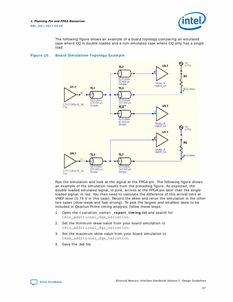
The following figure shows an example of a board topology comparing an emulatedcase where CQ is double-loaded and a non-emulated case where CQ only has a singleload.
Figure 10. Board Simulation Topology Example
Run the simulation and look at the signal at the FPGA pin. The following figure showsan example of the simulation results from the preceding figure. As expected, thedouble-loaded emulated signal, in pink, arrives at the FPGA pin later than the single-loaded signal, in red. You then need to calculate the difference of this arrival time atVREF level (0.75 V in this case). Record the skew and rerun the simulation in the othertwo cases (slow-weak and fast-strong). To pick the largest and smallest skew to beincluded in Quartus Prime timing analysis, follow these steps:
1. Open the <variation_name>_report_timing.tcl and search fortmin_additional_dqs_variation.
2. Set the minimum skew value from your board simulation totmin_additional_dqs_variation.
3. Set the maximum skew value from your board simulation totmax_additional_dqs_variation.
4. Save the .tcl file.
1. Planning Pin and FPGA Resources
EMI_DG | 2017.05.08
Send Feedback External Memory Interface Handbook Volume 2: Design Guidelines
57
Figure 11. Board Simulation Results
1.4.3. Pin-out Rule Exceptions for RLDRAM II and RLDRAM 3 Interfaces
RLDRAM II and RLDRAM 3 CIO devices have one bidirectional bus for the data, butthere are two different sets of clocks: one for read and one for write. As the QK andQK# already occupies the DQS and DQSn pins needed for read, placement of DK andDK# pins are restricted due to the limited number of pins in the FPGA. This limitationscauses the exceptions to the previous rules, which are discussed below.
The address or command pins of RLDRAM II must be placed in a DQ-group becausethese pins are driven by the PHY clock. Half-rate RLDRAM II interfaces and full-rateRLDRAM 3 interfaces use the PHY clock for both the DQ pins and the address orcommand pins.
1.4.3.1. Interfacing with ×9 RLDRAM II CIO Devices
RLDRAM 3 devices do not have the x9 configuration.
RLDRAM II devices have the following pins:
• 2 pins for QK and QK# signals
• 9 DQ pins (in a ×8/×9 DQS group)
• 2 pins for DK and DK# signals
• 1 DM pin
• 14 pins total (15 if you have a QVLD)
1. Planning Pin and FPGA Resources
EMI_DG | 2017.05.08
External Memory Interface Handbook Volume 2: Design Guidelines Send Feedback
58
In the FPGA, the ×8/×9 DQS group consists of 12 pins: 2 for the read clocks and 10for the data. In this case, move the QVLD (if you want to keep this connected eventhough this is not used in the Intel FPGA memory interface solution) and the DK andDK# pins to the adjacent DQS group. If that group is in use, move to any availableuser I/O pins in the same I/O bank.
1.4.3.2. Interfacing with ×18 RLDRAM II and RLDRAM 3 CIO Devices
This topic describes interfacing with x18 RLDRAM II and RLDRAM 3 devices.
RLDRAM II devices have the following pins:
• 4 pins for QK/QK# signals
• 18 DQ pins (in ×8/×9 DQS group)
• 2 pins for DK/DK# signals
• 1 DM pin
• 25 pins total (26 if you have a QVLD)
In the FPGA, you use two ×8/×9 DQS group totaling 24 pins: 4 for the read clocksand 18 for the read data.
Each ×8/×9 group has one DQ pin left over that can either use QVLD or DM, so one×8/×9 group has the DM pin associated with that group and one ×8/×9 group has theQVLD pin associated with that group.
RLDRAM 3 devices have the following pins:
• 4 pins for QK/QK# signals
• 18 DQ pins (in ×8/×9 DQS group)
• 4 pins for DK/DK# signals
• 2 DM pins
• 28 pins total (29 if you have a QVLD)
In the FPGA, you use two ×8/×9 DQS group totaling 24 pins: 4 for the read clocksand 18 for the read data.
Each ×8/×9 group has one DQ pin left over that can either use QVLD or DM, so one×8/×9 group has the DM pin associated with that group and one ×8/×9 group has theQVLD pin associated with that group.
1.4.3.3. Interfacing with RLDRAM II and RLDRAM 3 ×36 CIO Devices
This topic describes interfacing with RLDRAM II and RLDRAM 3 x36 CIO devices.
RLDRAM II devices have the following pins:
• 4 pins for QK/QK# signals
• 36 DQ pins (in x16/x18 DQS group)
• 4 pins for DK/DK# signals
• 1 DM pins
• 46 pins total (47 if you have a QVLD)
1. Planning Pin and FPGA Resources
EMI_DG | 2017.05.08
Send Feedback External Memory Interface Handbook Volume 2: Design Guidelines
59
In the FPGA, you use two ×16/×18 DQS groups totaling 48 pins: 4 for the read clocksand 36 for the read data. Configure each ×16/×18 DQS group to have:
• Two QK/QK# pins occupying the DQS/DQSn pins
• Pick two DQ pins in the ×16/×18 DQS groups that are DQS and DQSn pins in the×4 or ×8/×9 DQS groups for the DK and DK# pins
• 18 DQ pins occupying the DQ pins
• There are two DQ pins leftover that you can use for QVLD or DM pins. Put the DMpin in the group associated with DK[1] and the QVLD pin in the group associatedwith DK[0].
• Check that DM is associated with DK[1] for your chosen memory component.
RLDRAM 3 devices have the following pins:
• 8 pins for QK/QK# signals
• 36 DQ pins (in x8/x9 DQS group)
• 4 pins for DK/DK# signals
• 2 DM pins
• 48 pins total (49 if you have a QVLD)
In the FPGA, you use four ×8/×9 DQS groups.
In addition, observe the following placement rules for RLDRAM 3 interfaces:
For ×18 devices:
• Use two ×8/×9 DQS groups. Assign the QK/QK# pins and the DQ pins of the sameread group to the same DQS group.
• DQ, DM, and DK/DK# pins belonging to the same write group should be assignedto the same I/O sub-bank, for timing closure.
• Whenever possible, assign CK/CK# pins to the same I/O sub-bank as the DK/DK#pins, to improve tCKDK timing.
For ×36 devices:
• Use four ×8/×9 DQS groups. Assign the QK/QK# pins and the DQ pins of thesame read group to the same DQS group.
• DQ, DM, and DK/DK# pins belonging to the same write group should be assignedto the same I/O sub-bank, for timing closure.
• Whenever possible, assign CK/CK# pins to the same I/O sub-bank as the DK/DK#pins, to improve tCKDK timing.
1.4.4. Pin-out Rule Exceptions for QDR II and QDR II+ SRAM Burst-length-of-two Interfaces
If you are using the QDR II and QDR II+ SRAM burst-length-of-two devices, you maywant to place the address pins in a DQS group to minimize skew, because these pinsare now double data rate too.
1. Planning Pin and FPGA Resources
EMI_DG | 2017.05.08
External Memory Interface Handbook Volume 2: Design Guidelines Send Feedback
60
The address pins typically do not exceed 22 bits, so you may use one ×18 DQS groupsor two ×9 DQS groups on the same side of the device, if not the same I/O bank. InArria V GZ, Stratix III, Stratix IV, and Stratix V devices, one ×18 group typically has22 DQ bits and 2 pins for DQS/DQSn pins, while one ×9 group typically has 10 DQ bitswith 2 pins for DQS/DQSn pins. Using ×4 DQS groups should be a last resort.
1.4.5. Pin Connection Guidelines Tables
The following table lists the FPGA pin utilization for DDR, DDR2, and DDR3 SDRAMwithout leveling interfaces.
Table 11. FPGA Pin Utilization for DDR, DDR2, and DDR3 SDRAM without LevelingInterfaces
Interface PinDescription
Memory Device PinName
FPGA Pin Utilization
Arria II GX Arria II GZ,Stratix III, and
Stratix IV
Arria V, Cyclone V,
and Stratix V
MAX 10 FPGA
Memory SystemClock
CK and CK# (1) (2) If you are usingsingle-endedDQS signaling,place any unusedDQ or DQS pinswith DIFFOUTcapability locatedin the same bankor on the sameside as the datapins.If you are usingdifferential DQSsignaling inUniPHY IP, placeon DIFFOUT inthe same singleDQ group ofadequate widthto minimizeskew.
If you are usingsingle-endedDQS signaling,place anyDIFFOUT pins inthe same bank oron the same sideas the data pinsIf you are usingdifferential DQSsignaling inUniPHY IP, placeany DIFFOUTpins in the samebank or on thesame side as thedata pins. Ifthere are multipleCK/CK# pairs,place them onDIFFOUT in thesame single DQgroup ofadequate width.For example,DIMMs requiringthree memoryclock pin-pairsmust use a ×4DQS group.
If you are usingsingle-endedDQS signaling,place any unusedDQ or DQS pinswith DIFFOUTcapability in thesame bank or onthe same side asthe data pins.If you are usingdifferential DQSsignaling, placeany unused DQor DQS pins withDIFFOUTcapability for themem_clk[n:0]andmem_clk_n[n:0] signals (wheren>=0). CK andCK# pins mustuse a pin pairthat has DIFFOUTcapability.CK and CK# pinscan be in thesame group asother DQ or DQSpins. CK and CK#pins can beplaced such thatone signal of thedifferential pair isin a DQ groupand the othersignal is not.If there aremultiple CK andCK# pin pairs,place them onDIFFOUT in the
Place anydifferential I/Opin pair ( DIFFIO)in the same bankor on the sameside as the datapins.
continued...
1. Planning Pin and FPGA Resources
EMI_DG | 2017.05.08
Send Feedback External Memory Interface Handbook Volume 2: Design Guidelines
61
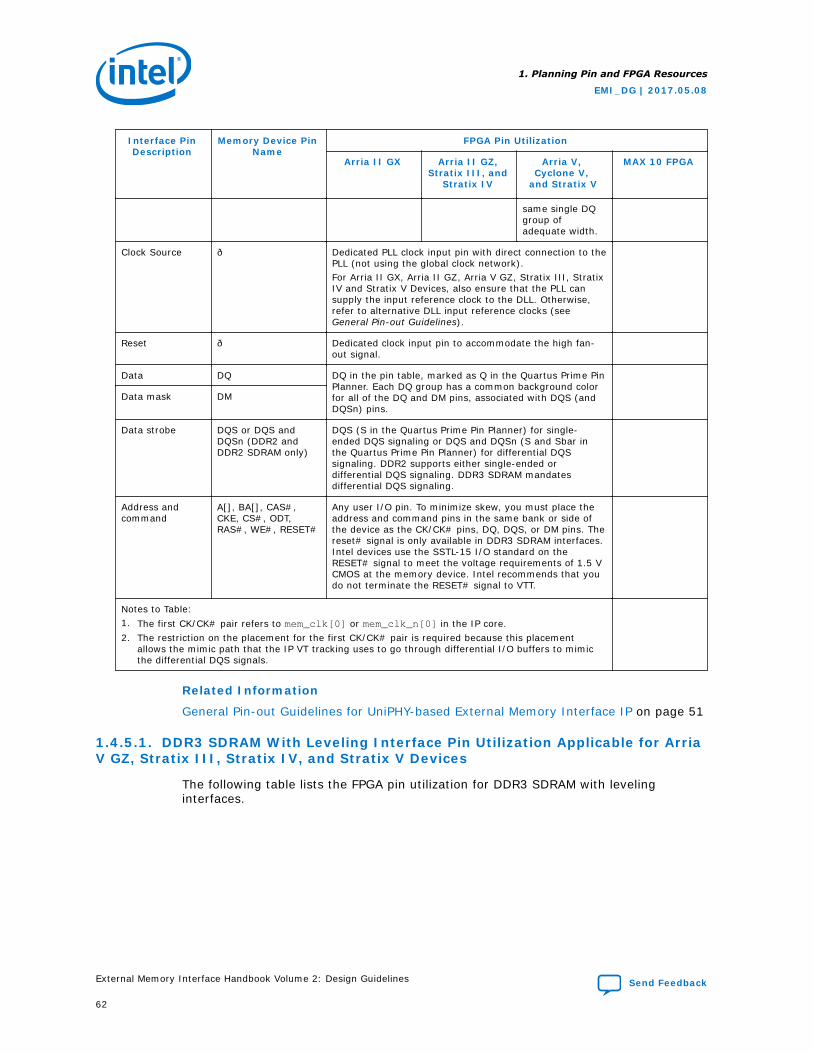
Interface PinDescription
Memory Device PinName
FPGA Pin Utilization
Arria II GX Arria II GZ,Stratix III, and
Stratix IV
Arria V, Cyclone V,
and Stratix V
MAX 10 FPGA
same single DQgroup ofadequate width.
Clock Source — Dedicated PLL clock input pin with direct connection to thePLL (not using the global clock network).For Arria II GX, Arria II GZ, Arria V GZ, Stratix III, StratixIV and Stratix V Devices, also ensure that the PLL cansupply the input reference clock to the DLL. Otherwise,refer to alternative DLL input reference clocks (seeGeneral Pin-out Guidelines).
Reset — Dedicated clock input pin to accommodate the high fan-out signal.
Data DQ DQ in the pin table, marked as Q in the Quartus Prime PinPlanner. Each DQ group has a common background colorfor all of the DQ and DM pins, associated with DQS (andDQSn) pins.
Data mask DM
Data strobe DQS or DQS andDQSn (DDR2 andDDR2 SDRAM only)
DQS (S in the Quartus Prime Pin Planner) for single-ended DQS signaling or DQS and DQSn (S and Sbar inthe Quartus Prime Pin Planner) for differential DQSsignaling. DDR2 supports either single-ended ordifferential DQS signaling. DDR3 SDRAM mandatesdifferential DQS signaling.
Address andcommand
A[], BA[], CAS#,CKE, CS#, ODT,RAS#, WE#, RESET#
Any user I/O pin. To minimize skew, you must place theaddress and command pins in the same bank or side ofthe device as the CK/CK# pins, DQ, DQS, or DM pins. Thereset# signal is only available in DDR3 SDRAM interfaces.Intel devices use the SSTL-15 I/O standard on theRESET# signal to meet the voltage requirements of 1.5 VCMOS at the memory device. Intel recommends that youdo not terminate the RESET# signal to VTT.
Notes to Table:1. The first CK/CK# pair refers to mem_clk[0] or mem_clk_n[0] in the IP core.2. The restriction on the placement for the first CK/CK# pair is required because this placement
allows the mimic path that the IP VT tracking uses to go through differential I/O buffers to mimicthe differential DQS signals.
Related Information
General Pin-out Guidelines for UniPHY-based External Memory Interface IP on page 51
1.4.5.1. DDR3 SDRAM With Leveling Interface Pin Utilization Applicable for ArriaV GZ, Stratix III, Stratix IV, and Stratix V Devices
The following table lists the FPGA pin utilization for DDR3 SDRAM with levelinginterfaces.
1. Planning Pin and FPGA Resources
EMI_DG | 2017.05.08
External Memory Interface Handbook Volume 2: Design Guidelines Send Feedback
62
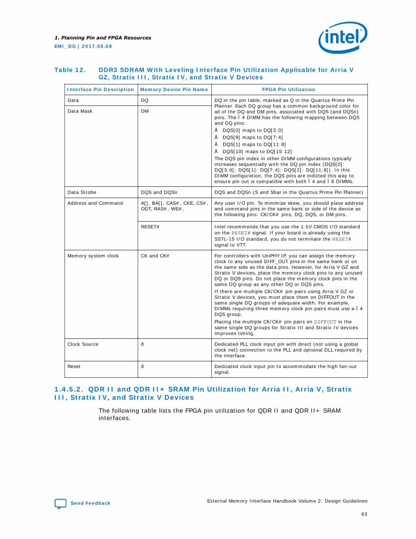
Table 12. DDR3 SDRAM With Leveling Interface Pin Utilization Applicable for Arria VGZ, Stratix III, Stratix IV, and Stratix V Devices
Interface Pin Description Memory Device Pin Name FPGA Pin Utilization
Data DQ DQ in the pin table, marked as Q in the Quartus Prime PinPlanner. Each DQ group has a common background color forall of the DQ and DM pins, associated with DQS (and DQSn)pins. The ×4 DIMM has the following mapping between DQSand DQ pins:• DQS[0] maps to DQ[3:0]• DQS[9] maps to DQ[7:4]• DQS[1] maps to DQ[11:8]• DQS[10] maps to DQ[15:12]The DQS pin index in other DIMM configurations typicallyincreases sequentially with the DQ pin index (DQS[0]:DQ[3:0]; DQS[1]: DQ[7:4]; DQS[2]: DQ[11:8]). In thisDIMM configuration, the DQS pins are indicted this way toensure pin out is compatible with both ×4 and ×8 DIMMs.
Data Mask DM
Data Strobe DQS and DQSn DQS and DQSn (S and Sbar in the Quartus Prime Pin Planner)
Address and Command A[], BA[], CAS#, CKE, CS#,ODT, RAS#, WE#,
Any user I/O pin. To minimize skew, you should place addressand command pins in the same bank or side of the device asthe following pins: CK/CK# pins, DQ, DQS, or DM pins.
RESET# Intel recommends that you use the 1.5V CMOS I/O standardon the RESET# signal. If your board is already using theSSTL-15 I/O standard, you do not terminate the RESET#signal to VTT.
Memory system clock CK and CK# For controllers with UniPHY IP, you can assign the memoryclock to any unused DIFF_OUT pins in the same bank or onthe same side as the data pins. However, for Arria V GZ andStratix V devices, place the memory clock pins to any unusedDQ or DQS pins. Do not place the memory clock pins in thesame DQ group as any other DQ or DQS pins.If there are multiple CK/CK# pin pairs using Arria V GZ orStratix V devices, you must place them on DIFFOUT in thesame single DQ groups of adequate width. For example,DIMMs requiring three memory clock pin-pairs must use a ×4DQS group.Placing the multiple CK/CK# pin pairs on DIFFOUT in thesame single DQ groups for Stratix III and Stratix IV devicesimproves timing.
Clock Source — Dedicated PLL clock input pin with direct (not using a globalclock net) connection to the PLL and optional DLL required bythe interface.
Reset — Dedicated clock input pin to accommodate the high fan-outsignal.
1.4.5.2. QDR II and QDR II+ SRAM Pin Utilization for Arria II, Arria V, StratixIII, Stratix IV, and Stratix V Devices
The following table lists the FPGA pin utilization for QDR II and QDR II+ SRAMinterfaces.
1. Planning Pin and FPGA Resources
EMI_DG | 2017.05.08
Send Feedback External Memory Interface Handbook Volume 2: Design Guidelines
63

Table 13. QDR II and QDR II+ SRAM Pin Utilization for Arria II, Arria V, Stratix III,Stratix IV, and Stratix V Devices
Interface Pin Description Memory Device Pin Name FPGA Pin Utilization
Read Clock CQ and CQ# (1) For QDR II SRAM devices with 1.5 or 2.5 cycles of readlatency or QDR II+ SRAM devices with 2.5 cycles of readlatency, connect CQ to DQS pin (S in the Quartus Prime PinPlanner), and CQn to CQn pin (Qbar in the Quartus Prime PinPlanner).For QDR II or QDR II+ SRAM devices with 2.0 cycles of readlatency, connect CQ to CQn pin (Qbar in the Quartus PrimePin Planner), and CQn to DQS pin (S in the Quartus Prime PinPlanner).Arria V devices do not use CQn. The CQ rising and fallingedges are used to clock the read data, instead of separate CQand CQn signals.
Read Data Q DQ pins (Q in the Quartus Prime Pin Planner). Ensure that youare using the DQ pins associated with the chosen read clockpins (DQS and CQn pins). QVLD pins are only available forQDR II+ SRAM devices and note that Intel FPGA IP does notuse the QVLD pin.
Data Valid QVLD
Memory and Write DataClock
K and K# Differential or pseudo-differential DQ, DQS, or DQSn pins inor near the write data group.
Write Data D DQ pins. Ensure that you are using the DQ pins associatedwith the chosen memory and write data clock pins (DQS andDQS pins).Byte Write Select BWS#, NWS#
Address and Command A, WPS#, RPS# Any user I/O pin. To minimize skew, you should place addressand command pins in the same bank or side of the device asthe following pins: K and K# pins, DQ, DQS, BWS#, andNWS# pins. If you are using burst-length-of-two devices,place the address signals in a DQS group pin as these signalsare now double data rate.
Clock source — Dedicated PLL clock input pin with direct (not using a globalclock net) connection to the PLL and optional DLL required bythe interface.
Reset — Dedicated clock input pin to accommodate the high fan-outsignal
Note to table:1. For Arria V designs with integer latency, connect the CQ# signal to the CQ/CQ# pins from the pin table and ignore the
polarity in the Pin Planner. For Arria V designs with fractional latency, connect the CQ signal to the CQ/CQ# pins fromthe pin table.
1.4.5.3. RLDRAM II CIO Pin Utilization for Arria II GZ, Arria V, Stratix III, StratixIV, and Stratix V Devices
The following table lists the FPGA pin utilization for RLDRAM II CIO and RLDRAM 3interfaces.
1. Planning Pin and FPGA Resources
EMI_DG | 2017.05.08
External Memory Interface Handbook Volume 2: Design Guidelines Send Feedback
64
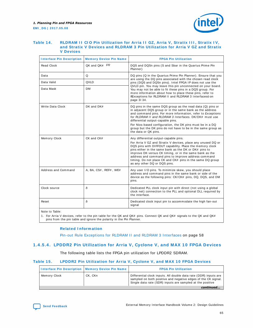
Table 14. RLDRAM II CIO Pin Utilization for Arria II GZ, Arria V, Stratix III, Stratix IV,and Stratix V Devices and RLDRAM 3 Pin Utilization for Arria V GZ and StratixV Devices
Interface Pin Description Memory Device Pin Name FPGA Pin Utilization
Read Clock QK and QK# (1) DQS and DQSn pins (S and Sbar in the Quartus Prime PinPlanner)
Data Q DQ pins (Q in the Quartus Prime Pin Planner). Ensure that youare using the DQ pins associated with the chosen read clockpins (DQS and DQSn pins). Intel FPGA IP does not use theQVLD pin. You may leave this pin unconnected on your board.You may not be able to fit these pins in a DQS group. Formore information about how to place these pins, refer to“Exceptions for RLDRAM II and RLDRAM 3 Interfaces” onpage 3–34.
Data Valid QVLD
Data Mask DM
Write Data Clock DK and DK# DQ pins in the same DQS group as the read data (Q) pins orin adjacent DQS group or in the same bank as the addressand command pins. For more information, refer to Exceptionsfor RLDRAM II and RLDRAM 3 Interfaces. DK/DK# must usedifferential output-capable pins.For Nios-based configuration, the DK pins must be in a DQgroup but the DK pins do not have to be in the same group asthe data or QK pins.
Memory Clock CK and CK# Any differential output-capable pins.For Arria V GZ and Stratix V devices, place any unused DQ orDQS pins with DIFFOUT capability. Place the memory clockpins either in the same bank as the DK or DK# pins toimprove DK versus CK timing, or in the same bank as theaddress and command pins to improve address commandtiming. Do not place CK and CK# pins in the same DQ groupas any other DQ or DQS pins.
Address and Command A, BA, CS#, REF#, WE# Any user I/O pins. To minimize skew, you should placeaddress and command pins in the same bank or side of thedevice as the following pins: CK/CK# pins, DQ, DQS, and DMpins.
Clock source — Dedicated PLL clock input pin with direct (not using a globalclock net) connection to the PLL and optional DLL required bythe interface.
Reset — Dedicated clock input pin to accommodate the high fan-outsignal
Note to Table:1. For Arria V devices, refer to the pin table for the QK and QK# pins. Connect QK and QK# signals to the QK and QK#
pins from the pin table and ignore the polarity in the Pin Planner.
Related Information
Pin-out Rule Exceptions for RLDRAM II and RLDRAM 3 Interfaces on page 58
1.4.5.4. LPDDR2 Pin Utilization for Arria V, Cyclone V, and MAX 10 FPGA Devices
The following table lists the FPGA pin utilization for LPDDR2 SDRAM.
Table 15. LPDDR2 Pin Utilization for Arria V, Cyclone V, and MAX 10 FPGA Devices
Interface Pin Description Memory Device Pin Name FPGA Pin Utilization
Memory Clock CK, CKn Differential clock inputs. All double data rate (DDR) inputs aresampled on both positive and negative edges of the CK signal.Single data rate (SDR) inputs are sampled at the positive
continued...
1. Planning Pin and FPGA Resources
EMI_DG | 2017.05.08
Send Feedback External Memory Interface Handbook Volume 2: Design Guidelines
65
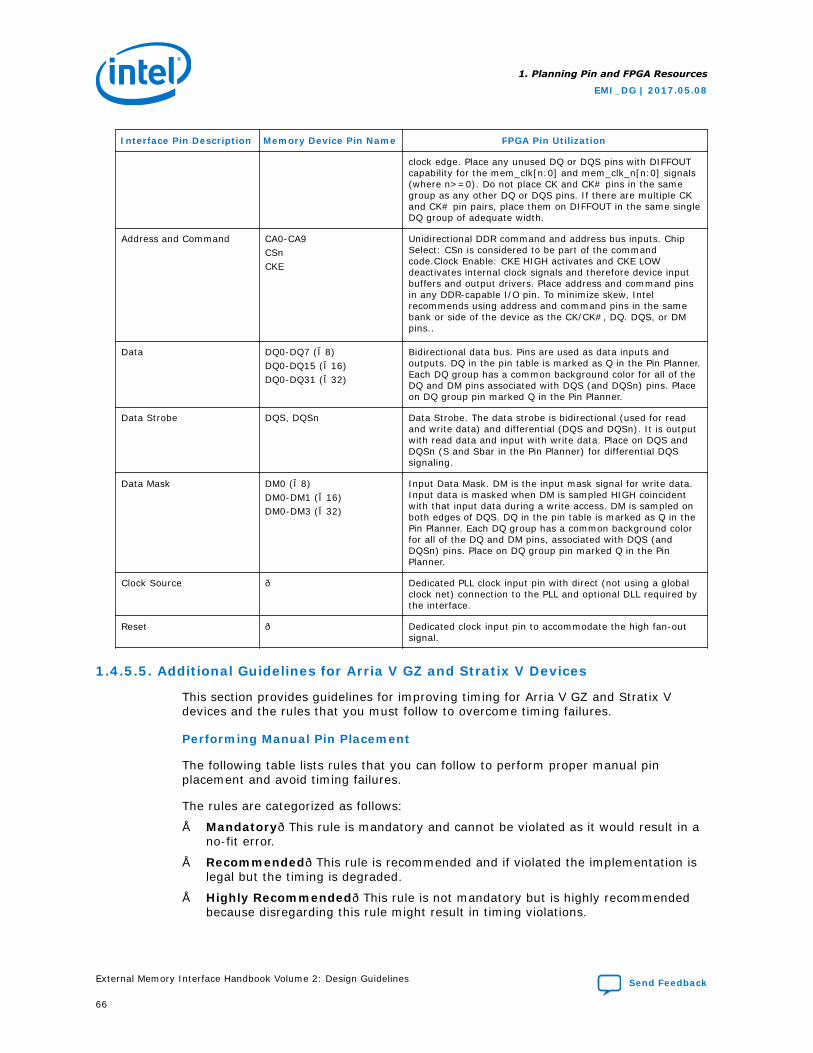
Interface Pin Description Memory Device Pin Name FPGA Pin Utilization
clock edge. Place any unused DQ or DQS pins with DIFFOUTcapability for the mem_clk[n:0] and mem_clk_n[n:0] signals(where n>=0). Do not place CK and CK# pins in the samegroup as any other DQ or DQS pins. If there are multiple CKand CK# pin pairs, place them on DIFFOUT in the same singleDQ group of adequate width.
Address and Command CA0-CA9CSnCKE
Unidirectional DDR command and address bus inputs. ChipSelect: CSn is considered to be part of the commandcode.Clock Enable: CKE HIGH activates and CKE LOWdeactivates internal clock signals and therefore device inputbuffers and output drivers. Place address and command pinsin any DDR-capable I/O pin. To minimize skew, Intelrecommends using address and command pins in the samebank or side of the device as the CK/CK#, DQ. DQS, or DMpins..
Data DQ0-DQ7 (×8)DQ0-DQ15 (×16)DQ0-DQ31 (×32)
Bidirectional data bus. Pins are used as data inputs andoutputs. DQ in the pin table is marked as Q in the Pin Planner.Each DQ group has a common background color for all of theDQ and DM pins associated with DQS (and DQSn) pins. Placeon DQ group pin marked Q in the Pin Planner.
Data Strobe DQS, DQSn Data Strobe. The data strobe is bidirectional (used for readand write data) and differential (DQS and DQSn). It is outputwith read data and input with write data. Place on DQS andDQSn (S and Sbar in the Pin Planner) for differential DQSsignaling.
Data Mask DM0 (×8)DM0-DM1 (×16)DM0-DM3 (×32)
Input Data Mask. DM is the input mask signal for write data.Input data is masked when DM is sampled HIGH coincidentwith that input data during a write access. DM is sampled onboth edges of DQS. DQ in the pin table is marked as Q in thePin Planner. Each DQ group has a common background colorfor all of the DQ and DM pins, associated with DQS (andDQSn) pins. Place on DQ group pin marked Q in the PinPlanner.
Clock Source — Dedicated PLL clock input pin with direct (not using a globalclock net) connection to the PLL and optional DLL required bythe interface.
Reset — Dedicated clock input pin to accommodate the high fan-outsignal.
1.4.5.5. Additional Guidelines for Arria V GZ and Stratix V Devices
This section provides guidelines for improving timing for Arria V GZ and Stratix Vdevices and the rules that you must follow to overcome timing failures.
Performing Manual Pin Placement
The following table lists rules that you can follow to perform proper manual pinplacement and avoid timing failures.
The rules are categorized as follows:
• Mandatory—This rule is mandatory and cannot be violated as it would result in ano-fit error.
• Recommended—This rule is recommended and if violated the implementation islegal but the timing is degraded.
• Highly Recommended—This rule is not mandatory but is highly recommendedbecause disregarding this rule might result in timing violations.
1. Planning Pin and FPGA Resources
EMI_DG | 2017.05.08
External Memory Interface Handbook Volume 2: Design Guidelines Send Feedback
66
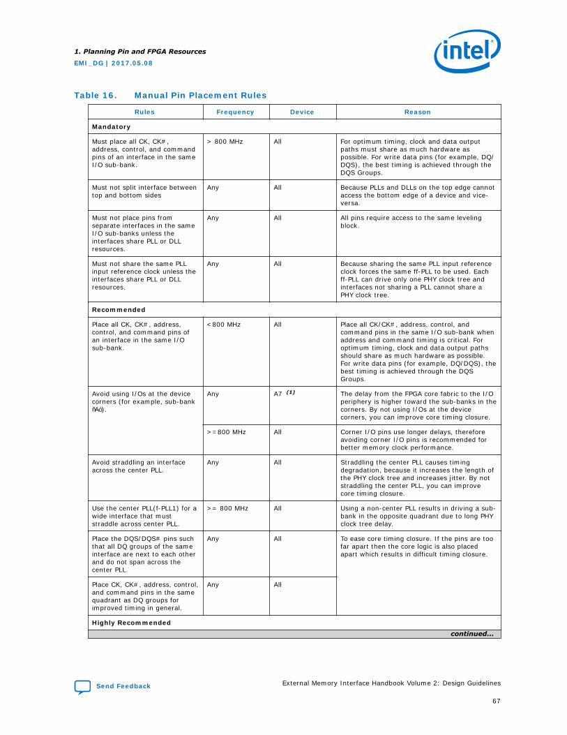
Table 16. Manual Pin Placement Rules
Rules Frequency Device Reason
Mandatory
Must place all CK, CK#,address, control, and commandpins of an interface in the sameI/O sub-bank.
> 800 MHz All For optimum timing, clock and data outputpaths must share as much hardware aspossible. For write data pins (for example, DQ/DQS), the best timing is achieved through theDQS Groups.
Must not split interface betweentop and bottom sides
Any All Because PLLs and DLLs on the top edge cannotaccess the bottom edge of a device and vice-versa.
Must not place pins fromseparate interfaces in the sameI/O sub-banks unless theinterfaces share PLL or DLLresources.
Any All All pins require access to the same levelingblock.
Must not share the same PLLinput reference clock unless theinterfaces share PLL or DLLresources.
Any All Because sharing the same PLL input referenceclock forces the same ff-PLL to be used. Eachff-PLL can drive only one PHY clock tree andinterfaces not sharing a PLL cannot share aPHY clock tree.
Recommended
Place all CK, CK#, address,control, and command pins ofan interface in the same I/Osub-bank.
<800 MHz All Place all CK/CK#, address, control, andcommand pins in the same I/O sub-bank whenaddress and command timing is critical. Foroptimum timing, clock and data output pathsshould share as much hardware as possible.For write data pins (for example, DQ/DQS), thebest timing is achieved through the DQSGroups.
Avoid using I/Os at the devicecorners (for example, sub-bank“A”).
Any A7 (1) The delay from the FPGA core fabric to the I/Operiphery is higher toward the sub-banks in thecorners. By not using I/Os at the devicecorners, you can improve core timing closure.
>=800 MHz All Corner I/O pins use longer delays, thereforeavoiding corner I/O pins is recommended forbetter memory clock performance.
Avoid straddling an interfaceacross the center PLL.
Any All Straddling the center PLL causes timingdegradation, because it increases the length ofthe PHY clock tree and increases jitter. By notstraddling the center PLL, you can improvecore timing closure.
Use the center PLL(f-PLL1) for awide interface that muststraddle across center PLL.
>= 800 MHz All Using a non-center PLL results in driving a sub-bank in the opposite quadrant due to long PHYclock tree delay.
Place the DQS/DQS# pins suchthat all DQ groups of the sameinterface are next to each otherand do not span across thecenter PLL.
Any All To ease core timing closure. If the pins are toofar apart then the core logic is also placedapart which results in difficult timing closure.
Place CK, CK#, address, control,and command pins in the samequadrant as DQ groups forimproved timing in general.
Any All
Highly Recommendedcontinued...
1. Planning Pin and FPGA Resources
EMI_DG | 2017.05.08
Send Feedback External Memory Interface Handbook Volume 2: Design Guidelines
67
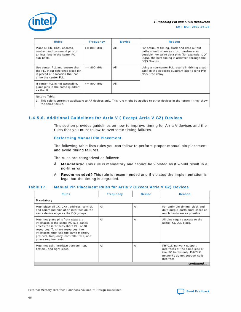
Rules Frequency Device Reason
Place all CK, CK#, address,control, and command pins ofan interface in the same I/Osub-bank.
>= 800 MHz All For optimum timing, clock and data outputpaths should share as much hardware aspossible. For write data pins (for example, DQ/DQS), the best timing is achieved through theDQS Groups.
Use center PLL and ensure thatthe PLL input reference clock pinis placed at a location that candrive the center PLL.
>= 800 MHz All Using a non-center PLL results in driving a sub-bank in the opposite quadrant due to long PHYclock tree delay.
If center PLL is not accessible,place pins in the same quadrantas the PLL.
>= 800 MHz All
Note to Table:1. This rule is currently applicable to A7 devices only. This rule might be applied to other devices in the future if they show
the same failure.
1.4.5.6. Additional Guidelines for Arria V ( Except Arria V GZ) Devices
This section provides guidelines on how to improve timing for Arria V devices and therules that you must follow to overcome timing failures.
Performing Manual Pin Placement
The following table lists rules you can follow to perform proper manual pin placementand avoid timing failures.
The rules are categorized as follows:
• Mandatory—This rule is mandatory and cannot be violated as it would result in ano-fit error.
• Recommended—This rule is recommended and if violated the implementation islegal but the timing is degraded.
Table 17. Manual Pin Placement Rules for Arria V (Except Arria V GZ) Devices
Rules Frequency Device Reason
Mandatory
Must place all CK, CK#, address, control,and command pins of an interface on thesame device edge as the DQ groups.
All All For optimum timing, clock anddata output ports must share asmuch hardware as possible.
Must not place pins from separateinterfaces in the same I/O sub-banksunless the interfaces share PLL or DLLresources. To share resources, theinterfaces must use the same memoryprotocol, frequency, controller rate, andphase requirements.
All All All pins require access to thesame PLL/DLL block.
Must not split interface between top,bottom, and right sides.
All All PHYCLK network supportinterfaces at the same side ofthe I/O banks only. PHYCLKnetworks do not support splitinterface.
continued...
1. Planning Pin and FPGA Resources
EMI_DG | 2017.05.08
External Memory Interface Handbook Volume 2: Design Guidelines Send Feedback
68
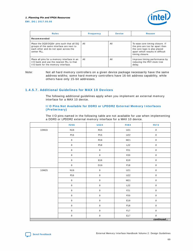
Rules Frequency Device Reason
Recommended
Place the DQS/DQS# pins such that all DQgroups of the same interface are next toeach other and do not span across thecenter PLL.
All All To ease core timing closure. Ifthe pins are too far apart thenthe core logic is also placedapart which results in difficulttiming closure.
Place all pins for a memory interface in anI/O bank and use the nearest PLL to thatI/O bank for the memory interface.
All All Improve timing performance byreducing the PHY clock treedelay.
Note: Not all hard memory controllers on a given device package necessarily have the sameaddress widths; some hard memory controllers have 16-bit address capability, whileothers have only 15-bit addresses.
1.4.5.7. Additional Guidelines for MAX 10 Devices
The following additional guidelines apply when you implement an external memoryinterface for a MAX 10 device.
I/O Pins Not Available for DDR3 or LPDDR2 External Memory Interfaces(Preliminary)
The I/O pins named in the following table are not available for use when implementinga DDR3 or LPDDR2 external memory interface for a MAX 10 device.
F256 U324 F484 F672
10M16 N16 R15 U21 —
P16 P15 U22 —
— R18 M21 —
— P18 L22 —
— — F21 —
— — F20 —
— E16 E19 —
— D16 F18 —
10M25 N16 — U21 —
P16 — U22 —
— — M21 —
— — L22 —
— — F21 —
— — F20 —
— — E19 —
— — F18 —
— — F17 —
— — E17 —
continued...
1. Planning Pin and FPGA Resources
EMI_DG | 2017.05.08
Send Feedback External Memory Interface Handbook Volume 2: Design Guidelines
69
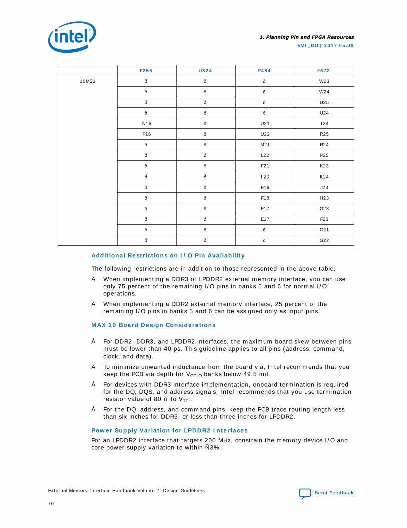
F256 U324 F484 F672
10M50 — — — W23
— — — W24
— — — U25
— — — U24
N16 — U21 T24
P16 — U22 R25
— — M21 R24
— — L22 P25
— — F21 K23
— — F20 K24
— — E19 J23
— — F18 H23
— — F17 G23
— — E17 F23
— — — G21
— — — G22
Additional Restrictions on I/O Pin Availability
The following restrictions are in addition to those represented in the above table.
• When implementing a DDR3 or LPDDR2 external memory interface, you can useonly 75 percent of the remaining I/O pins in banks 5 and 6 for normal I/Ooperations.
• When implementing a DDR2 external memory interface, 25 percent of theremaining I/O pins in banks 5 and 6 can be assigned only as input pins.
MAX 10 Board Design Considerations
• For DDR2, DDR3, and LPDDR2 interfaces, the maximum board skew between pinsmust be lower than 40 ps. This guideline applies to all pins (address, command,clock, and data).
• To minimize unwanted inductance from the board via, Intel recommends that youkeep the PCB via depth for VCCIO banks below 49.5 mil.
• For devices with DDR3 interface implementation, onboard termination is requiredfor the DQ, DQS, and address signals. Intel recommends that you use terminationresistor value of 80 Ω to VTT.
• For the DQ, address, and command pins, keep the PCB trace routing length lessthan six inches for DDR3, or less than three inches for LPDDR2.
Power Supply Variation for LPDDR2 InterfacesFor an LPDDR2 interface that targets 200 MHz, constrain the memory device I/O andcore power supply variation to within ±3%.
1. Planning Pin and FPGA Resources
EMI_DG | 2017.05.08
External Memory Interface Handbook Volume 2: Design Guidelines Send Feedback
70
1.4.5.8. Additional Guidelines for Cyclone V Devices
This topic provides guidelines for improving performance for Cyclone V devices.
I/O Pins Connect to Ground for Hard Memory Interface Operation
According to the Cyclone V pin-out file, there are some general I/O pins that areconnected to ground for hard memory interface operation. These I/O pins should begrounded to reduce crosstalk from neighboring I/O pins and to ensure theperformance of the hard memory interface.
The grounded user I/O pins can also be used as regular I/O pins if you run short ofavailable I/O pins; however, the hard memory interface performance will be reduced ifthese pins are not connected to ground.
1.4.6. PLLs and Clock Networks
The exact number of clocks and PLLs required in your design depends greatly on thememory interface frequency, and on the IP that your design uses.
For example, you can build simple DDR slow-speed interfaces that typically requireonly two clocks: system and write. You can then use the rising and falling edges ofthese two clocks to derive four phases (0°, 90°, 180°, and 270°). However, as clockspeeds increase, the timing margin decreases and additional clocks are required, tooptimize setup and hold and meet timing. Typically, at higher clock speeds, you needto have dedicated clocks for resynchronization, and address and command paths.
Intel FPGA memory interface IP uses one PLL, which generates the various clocksneeded in the memory interface data path and controller, and provides the requiredphase shifts for the write clock and address and command clock. The PLL isinstantiated when you generate the Intel FPGA memory IPs.
By default, the memory interface IP uses the PLL to generate the input reference clockfor the DLL, available in all supported device families. This method eliminates the needof an extra pin for the DLL input reference clock.
The input reference clock to the DLL can come from certain input clock pins or clockoutput from certain PLLs.
Note: Intel recommends using integer PLLs for memory interfaces; handbook specificationsare based on integer PLL implementations.
For the actual pins and PLLs connected to the DLLs, refer to the External MemoryInterfaces chapter of the relevant device family handbook.
You must use the PLL located in the same device quadrant or side as the memoryinterface and the corresponding dedicated clock input pin for that PLL, to ensureoptimal performance and accurate timing results from the Quartus Prime software.
The input clock to the PLL can fan out to logic other than the PHY, so long as the clockinput pin to the PLL is a dedicated input clock path, and you ensure that the clockdomain transfer between UniPHY and the core logic is clocked by the reference clockgoing into a global clock.
1. Planning Pin and FPGA Resources
EMI_DG | 2017.05.08
Send Feedback External Memory Interface Handbook Volume 2: Design Guidelines
71
1.4.6.1. Number of PLLs Available in Intel Device Families
The following table lists the number of PLLs available in Intel device families.
Table 18. Number of PLLs Available in Intel Device Families
Device Family Enhanced PLLs Available
Arria II GX 4-6
Arria II GZ 3-8
Arria V 16-24
Arria V GZ (fPLL) 22-28
Cyclone V 4-8
MAX 10 FPGA 1-4
Stratix III 4-12
Stratix IV 3-12
Stratix V (fPLL) 22-28
Note to Table:1. For more details, refer to the Clock Networks and PLL chapter of the respective device family handbook.
1.4.6.2. Number of Enhanced PLL Clock Outputs and Dedicated Clock OutputsAvailable in Intel Device Families
The following table lists the number of enhanced PLL clock outputs and dedicatedclock outputs available in Intel device families.
Table 19. Number of Enhanced PLL Clock Outputs and Dedicated Clock OutputsAvailable in Intel Device Families (1)
Device Family Number of Enhanced PLL ClockOutputs
Number Dedicated Clock Outputs
Arria II GX (2) 7 clock outputs each 1 single-ended or 1 differential pair3 single-ended or 3 differential pair total (3)
Arria V 18 clock outputs each 4 single-ended or 2 single-ended and 1 differentialpair
Stratix III Left/right: 7 clock outputsTop/bottom: 10 clock outputs
Left/right: 2 single-ended or 1 differential pairTop/bottom: 6 single-ended or 4 single-ended and1 differential pair
Arria II GZ and Stratix IV Left/right: 7 clock outputsTop/bottom: 10 clock outputs
Left/right: 2 single-ended or 1 differential pairTop/bottom: 6 single-ended or 4 single-ended and1 differential pair
Arria V GZ and Stratix V 18 clock outputs each 4 single-ended or 2 single-ended and 1 differentialpair
Notes to Table:1. For more details, refer to the Clock Networks and PLL chapter of the respective device family handbook.2. PLL_5 and PLL_6 of Arria II GX devices do not have dedicated clock outputs.3. The same PLL clock outputs drives three single-ended or three differential I/O pairs, which are only supported in PLL_1
and PLL_3 of the EP2AGX95, EP2AGX125, EP2AGX190, and EP2AGX260 devices.
1. Planning Pin and FPGA Resources
EMI_DG | 2017.05.08
External Memory Interface Handbook Volume 2: Design Guidelines Send Feedback
72
1.4.6.3. Number of Clock Networks Available in Intel Device Families
The following table lists the number of clock networks available in Intel devicefamilies.
Table 20. Number of Clock Networks Available in Intel Device Families (1)
Device Family Global Clock Network Regional Clock Network
Arria II GX 16 48
Arria II GZ 16 64–88
Arria V 16 88
Arria V GZ 16 92
Cyclone V 16 N/A
MAX 10 FPGA 10
Stratix III 16 64–88
Stratix IV 16 64–88
Stratix V 16 92
Note to Table:1. For more information on the number of available clock network resources per device quadrant to better understand the
number of clock networks available for your interface, refer to the Clock Networks and PLL chapter of the respectivedevice family handbook.
Note: You must decide whether you need to share clock networks, PLL clock outputs, or PLLsif you are implementing multiple memory interfaces.
1.4.6.4. Clock Network Usage in UniPHY-based Memory Interfaces—DDR2 andDDR3 SDRAM (1) (2)
The following table lists clock network usage in UniPHY-based memory interfaces forDDR2 and DDR3 protocols.
Table 21. Clock Network Usage in UniPHY-based Memory Interfaces—DDR2 and DDR3SDRAM
Device DDR3 SDRAM DDR2 SDRAM
Half-Rate Half-Rate
Number of full-rateclock
Number of half-rateclock
Number of full-rateclock
Number of half-rateclock
Stratix III 3 global 1 global1 regional
1 global2 global
1 global1 regional
Arria II GZ and StratixIV
3 global 1 global1 regional
1 regional2 regional
1 global1 regional
Arria V GZ and StratixV
1 global2 regional
2 global 1 regional2 regional
2 global
Notes to Table:1. There are two additional regional clocks, pll_avl_clk and pll_config_clk for DDR2 and DDR3 SDRAM with
UniPHY memory interfaces.2. In multiple interface designs with other IP, the clock network might need to be modified to get a design to fit. For more
information, refer to the Clock Networks and PLLs chapter in the respective device handbooks.
1. Planning Pin and FPGA Resources
EMI_DG | 2017.05.08
Send Feedback External Memory Interface Handbook Volume 2: Design Guidelines
73
1.4.6.5. Clock Network Usage in UniPHY-based Memory Interfaces—RLDRAM II,and QDR II and QDR II+ SRAM
The following table lists clock network usage in UniPHY-based memory interfaces forRLDRAM II, QDR II, and QDR II+ protocols.
Table 22. Clock Network Usage in UniPHY-based Memory Interfaces—RLDRAM II, andQDR II and QDR II+ SRAM
Device RLDRAM II QDR II/QDR II+ SRAM
Half-Rate Full-Rate Half-Rate Full-Rate
Number offull-rate clock
Number ofhalf-rate clock
Number offull-rate clock
Number offull-rate clock
Number ofhalf-rate clock
Number offull-rate clock
Arria II GX — — — 2 global 2 global 4 global
Stratix III 2 regional 1 global1 regional
1 global2 regional
1 global1 regional
2 regional 1 global2 regional
Arria II GZ andStratix IV
2 regional 1 global1 regional
1 global2 regional
1 global1 regional
2 regional 1 global2 regional
Note: For more information about the clocks used in UniPHY-based memory standards, referto the Functional Description—UniPHY chapter in volume 3 of the External MemoryInterface Handbook.
Related Information
Functional Description—UniPHY
1.4.6.6. PLL Usage for DDR, DDR2, and DDR3 SDRAM Without LevelingInterfaces
The following table lists PLL usage for DDR, DDR2, and DDR3 protocols withoutleveling interfaces.
Table 23. PLL Usage for DDR, DDR2, and DDR3 SDRAM Without Leveling Interfaces
Clock Arria II GX Devices Stratix III and Stratix IV Devices
C0 • phy_clk_1x in half-rate designs• aux_half_rate_clk
• PLL scan_clk
• phy_clk_1x in half-rate designs• aux_half_rate_clk
• PLL scan_clk
C1 • phy_clk_1x in full-rate designs• aux_full_rate_clk
• mem_clk_2x to generate DQS and CK/CK# signals• ac_clk_2x
• cs_n_clk_2x
• mem_clk_2x
C2 • Unused • phy_clk_1x in full-rate designs• aux_full_rate_clk
C3 • write_clk_2x (for DQ)• ac_clk_2x
• cs_n_clk_2x
• write_clk_2x
continued...
1. Planning Pin and FPGA Resources
EMI_DG | 2017.05.08
External Memory Interface Handbook Volume 2: Design Guidelines Send Feedback
74
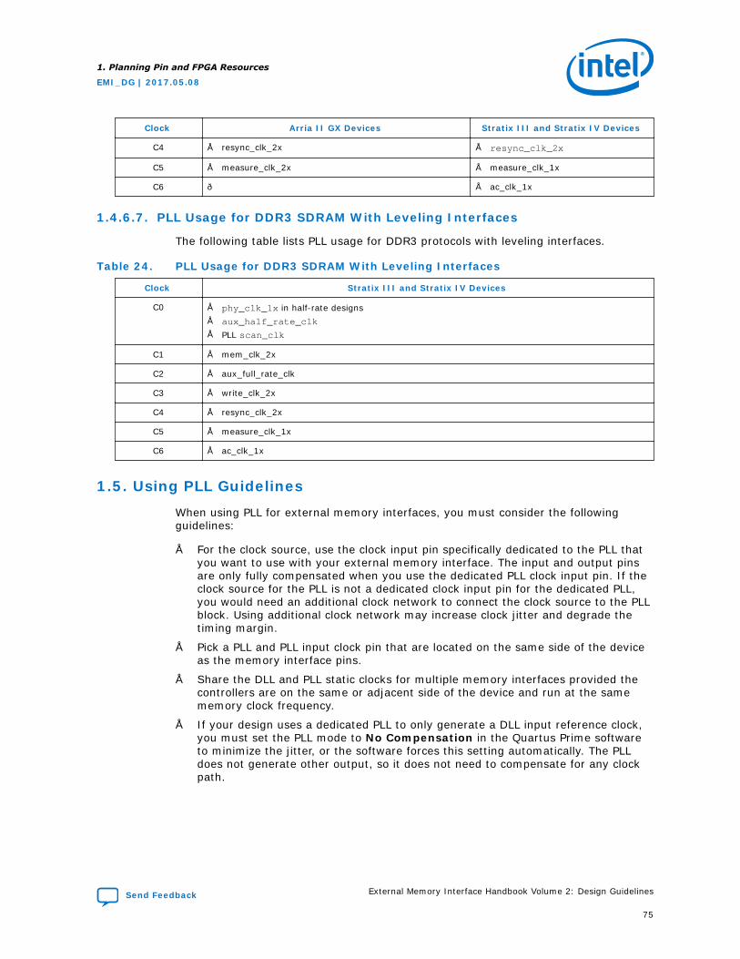
Clock Arria II GX Devices Stratix III and Stratix IV Devices
C4 • resync_clk_2x • resync_clk_2x
C5 • measure_clk_2x • measure_clk_1x
C6 — • ac_clk_1x
1.4.6.7. PLL Usage for DDR3 SDRAM With Leveling Interfaces
The following table lists PLL usage for DDR3 protocols with leveling interfaces.
Table 24. PLL Usage for DDR3 SDRAM With Leveling Interfaces
Clock Stratix III and Stratix IV Devices
C0 • phy_clk_1x in half-rate designs• aux_half_rate_clk
• PLL scan_clk
C1 • mem_clk_2x
C2 • aux_full_rate_clk
C3 • write_clk_2x
C4 • resync_clk_2x
C5 • measure_clk_1x
C6 • ac_clk_1x
1.5. Using PLL Guidelines
When using PLL for external memory interfaces, you must consider the followingguidelines:
• For the clock source, use the clock input pin specifically dedicated to the PLL thatyou want to use with your external memory interface. The input and output pinsare only fully compensated when you use the dedicated PLL clock input pin. If theclock source for the PLL is not a dedicated clock input pin for the dedicated PLL,you would need an additional clock network to connect the clock source to the PLLblock. Using additional clock network may increase clock jitter and degrade thetiming margin.
• Pick a PLL and PLL input clock pin that are located on the same side of the deviceas the memory interface pins.
• Share the DLL and PLL static clocks for multiple memory interfaces provided thecontrollers are on the same or adjacent side of the device and run at the samememory clock frequency.
• If your design uses a dedicated PLL to only generate a DLL input reference clock,you must set the PLL mode to No Compensation in the Quartus Prime softwareto minimize the jitter, or the software forces this setting automatically. The PLLdoes not generate other output, so it does not need to compensate for any clockpath.
1. Planning Pin and FPGA Resources
EMI_DG | 2017.05.08
Send Feedback External Memory Interface Handbook Volume 2: Design Guidelines
75
• If your design cascades PLL, the source (upstream) PLL must have alow-bandwidth setting, while the destination (downstream) PLL must have ahigh-bandwidth setting to minimize jitter. Intel does not recommend usingcascaded PLLs for external memory interfaces because your design getsaccumulated jitters. The memory output clock may violate the memory devicejitter specification.
• Use cascading PLLs at your own risk. For more information, refer to “PLLCascading”.
• If you are using Arria II GX devices, for a single memory instance that spans tworight-side quadrants, use a middle-side PLL as the source for that interface.
• If you are using Arria II GZ, Arria V GZ, Stratix III, Stratix IV, or Stratix V devices,for a single memory instance that spans two top or bottom quadrants, use amiddle top or bottom PLL as the source for that interface. The ten dual regionalclocks that the single interface requires must not block the design using theadjacent PLL (if available) for a second interface.
Related Information
PLL Cascading on page 76
1.6. PLL Cascading
Arria II GZ PLLs, Stratix III PLLs, Stratix IV PLLs, Stratix V and Arria V GZ fractionalPLLs (fPLLs), and the two middle PLLs in Arria II GX EP2AGX95, EP2AGX125,EP2AGX190, and EP2AGX260 devices can be cascaded using either the global orregional clock trees, or the cascade path between two adjacent PLLs.
Note: Use cascading PLLs at your own risk. You should use faster memory devices tomaximize timing margins.
The UniPHY IP supports PLL cascading using the cascade path without any additionaltiming derating when the bandwidth and compensation rules are followed. The timingconstraints and analysis assume that there is no additional jitter due to PLL cascadingwhen the upstream PLL uses no compensation and low bandwidth, and thedownstream PLL uses no compensation and high bandwidth.
The UniPHY IP does not support PLL cascading using the global and regional clocknetworks. You can implement PLL cascading at your own risk without any additionalguidance and specifications from Intel. The Quartus Prime software does issue acritical warning suggesting use of the cascade path to minimize jitter, but does notexplicitly state that Intel does not support cascading using global and regional clocknetworks.
Some Arria II GX devices (EP2AGX95, EP2AGX125, EP2AGX190, and EP2AGX260)have direct cascade path for two middle right PLLs. Arria II GX PLLs have the samebandwidth options as Stratix IV GX left and right PLLs.
The Arria 10 External Memory Interface IP does not support PLL cascading.
1.7. DLL
The Intel FPGA memory interface IP uses one DLL. The DLL is located at the corner ofthe device and can send the control signals to shift the DQS pins on its adjacent sidesfor Stratix-series devices, or DQS pins in any I/O banks in Arria II GX devices.
1. Planning Pin and FPGA Resources
EMI_DG | 2017.05.08
External Memory Interface Handbook Volume 2: Design Guidelines Send Feedback
76
For example, the top-left DLL can shift DQS pins on the top side and left side of thedevice. The DLL generates the same phase shift resolution for both sides, but cangenerate different phase offset to the two different sides, if needed. Each DQS pin canbe configured to use or ignore the phase offset generated by the DLL.
The DLL cannot generate two different phase offsets to the same side of the device.However, you can use two different DLLs to for this functionality.
DLL reference clocks must come from either dedicated clock input pins located oneither side of the DLL or from specific PLL output clocks. Any clock running at thememory frequency is valid for the DLLs.
To minimize the number of clocks routed directly on the PCB, typically this referenceclock is sourced from the memory controllers PLL. In general, DLLs can use the PLLsdirectly adjacent to them (corner PLLs when available) or the closest PLL located inthe two sides adjacent to its location.
Note: By default, the DLL reference clock in Intel FPGA external memory IP is from a PLLoutput.
When designing for 780-pin packages with EP3SE80, EP3SE110, EP3SL150,EP4SE230, EP4SE360, EP4SGX180, and EP4SGX230 devices, the PLL to DLL referenceclock connection is limited. DLL2 is isolated from a direct PLL connection and can onlyreceive a reference clock externally from pins CLK[11:4]p in EP3SE80, EP3SE110,EP3SL150, EP4SE230, and EP4SE360 devices. In EP4SGX180 and EP4SGX230 devices,DLL2 and DLL3 are not directly connected to PLL. DLL2 and DLL3 receive a referenceclock externally from pins CLK[7:4]p and CLK[15:12]p respectively.
For more DLL information, refer to the respective device handbooks.
The DLL reference clock should be the same frequency as the memory interface, butthe phase is not important.
The required DQS capture phase is optimally chosen based on operating frequencyand external memory interface type (DDR, DDR2, DDR3 SDRAM, and QDR II SRAM, orRLDRAM II). As each DLL supports two possible phase offsets, two different memoryinterface types operating at the same frequency can easily share a single DLL. Moremay be possible, depending on the phase shift required.
Intel FPGA memory IP always specifies a default optimal phase setting, to overridethis setting, refer to Implementing and Parameterizing Memory IP .
When sharing DLLs, your memory interfaces must be of the same frequency. If therequired phase shift is different amongst the multiple memory interfaces, you can usea different delay chain in the DQS logic block or use the DLL phase offset feature.
To simplify the interface to IP connections, multiple memory interfaces operating atthe same frequency usually share the same system and static clocks as each otherwhere possible. This sharing minimizes the number of dedicated clock nets requiredand reduces the number of different clock domains found within the same design.
As each DLL can directly drive four banks, but each PLL only has complete C (output)counter coverage of two banks (using dual regional networks), situations can occurwhere a second PLL operating at the same frequency is required. As cascaded PLLsincrease jitter and reduce timing margin, you are advised to first ascertain if analternative second DLL and PLL combination is not available and more optimal.
1. Planning Pin and FPGA Resources
EMI_DG | 2017.05.08
Send Feedback External Memory Interface Handbook Volume 2: Design Guidelines
77
Select a DLL that is available for the side of the device where the memory interfaceresides. If you select a PLL or a PLL input clock reference pin that can also serve asthe DLL input reference clock, you do not need an extra input pin for the DLL inputreference clock.
Related Information
Implementing and Parameterizing Memory IP on page 184
1.8. Other FPGA Resources
The Intel FPGA memory interface IP uses FPGA fabric, including registers and theMemory Block to implement the memory interface.
For resource utilization examples to ensure that you can fit your other modules in thedevice, refer to the “Resource Utilization” section in the Introduction to UniPHY IPchapter of the External Memory Interface Handbook.
One OCT calibration block is used if you are using the FPGA OCT feature in thememory interface.The OCT calibration block uses two pins (RUP and RDN), or singlepin (RZQ) (“OCT Support for Arria II GX, Arria II GZ, Arria V, Arria V GZ, Cyclone V,Stratix III, Stratix IV, and Stratix V Devices”). You can select any of the available OCTcalibration block as you do not need to place this block in the same bank or deviceside of your memory interface. The only requirement is that the I/O bank where youplace the OCT calibration block uses the same VCCIO voltage as the memoryinterface. You can share multiple memory interfaces with the same OCT calibrationblock if the VCCIO voltage is the same.
Related Information
OCT Support on page 37
1.9. Document Revision History
Date Version Changes
May 2017 2017.05.08 • Added Guidelines for Stratix 10 ExternalMemory Interface IP, General Pin-OutGuidelines for Stratix 10 EMIF IP, andResource Sharing Guidelines for Stratix 10EMIF IP sections.
• Rebranded as Intel.
October 2016 2016.10.31 • Removed paragraph from Address andCommand description in several pin utilizationtables.
May 2016 2016.05.02 • Modified Data Strobe and Address data inUDIMM, RDIMM, and LRDIMM Pin Options forDDR4 table in DDR, DDR2, DDR3, and DDR4SDRAM DIMM Options. Added notes to table.
continued...
1. Planning Pin and FPGA Resources
EMI_DG | 2017.05.08
External Memory Interface Handbook Volume 2: Design Guidelines Send Feedback
78
Date Version Changes
November 2015 2015.11.02 • Changed instances of Quartus II to QuartusPrime.
• Modified I/O Banks Selection, PLL ReferenceClock and RZQ Pins Placement, and Ping PongPHY Implementation sections in General Pin-Out Guidelines for Arria 10 EMIF IP.
• Added Additional Requirements for DDR3 andDDR4 Ping-Pong PHY Interfaces in GeneralPin-Out Guidelines for Arria 10 EMIF IP.
• Removed references to OCT Blocks fromResource Sharing Guidelines for Arria 10 EMIFIP section.
• Added LPDDR3.
May 2015 2015.05.04 • Removed the F672 package of the 10M25device.
• Updated the additional guidelines for MAX 10devices to improve clarity.
• Added related information link to the MAX 10FPGA Signal Integrity Design Guidelines forthe Additional Guidelines for MAX 10 Devicestopic.
December 2014 2014.12.15 • General Pin-Out Guidelines for Arria 10 EMIFIP section:— Added note to step 10.— Removed steps 13 and 14.— Added a bullet point to Address/Command
Pins Location.— Added Ping Pong PHY Implementation— Added parenthetical comment to fifth
bullet point in I/O Banks Selection— Added note following the procedure,
advising that all pins in a DQS groupshould reside in the same I/O bank, forRLDRAM II and RLDRAM 3 interfaces.
• Added QDR IV SRAM Clock Signals, QDR IVSRAM Commands and Addresses, AP, andAINV Signals, and QDR IV SRAM Data, DINV,and QVLD Signals topics.
• Added note to Estimating Pin Requirementssection.
• DDR, DDR2, DDR3, and DDR4 SDRAM DIMMOptions section:— Added UDIMM, RDIMM, and LRDIMM Pin
Options for DDR4 table.— Changed notes to LRDIMM Pin Options for
DDR, DDR2, and DDR3 table.— Removed reference to Chip ID pin.
continued...
1. Planning Pin and FPGA Resources
EMI_DG | 2017.05.08
Send Feedback External Memory Interface Handbook Volume 2: Design Guidelines
79
Date Version Changes
August 2014 2014.08.15 • Made several changes to Pin Counts forVarious Example Memory Interfaces table:— Added DDR4 SDRAM and RLDRAM 3 CIO.— Removed x72 rows from table entries for
DDR, DDR2, and DDR3.— Added Arria 10 to note 11.— Added notes 12-18.
• Added DDR4 to descriptions of:— Clock signals— Command and address signals— Data, data strobe, DM/DBI, and optional
ECC signals— SDRAM DIMM options
• Added QDR II+ Xtreme to descriptions of:— SRAM clock signals— SRAM command signals— SRAM address signals— SRAM data, BWS, and QVLD signals
• Changed title of section OCT Support for ArriaII GX, Arria II GZ, Arria V, Arria V GZ, CycloneV, Stratix III, Stratix IV, and Stratix V Devicesto OCT Support.
• Reorganized chapter to have separate sectionsfor Guidelines for Arria 10 External MemoryInterface IP and Guidelines for UniPHY-basedExternal Memory Interface IP.
• Revised Arria 10-specific guidelines.
December 2013 2013.12.16 • Removed references to ALTMEMPHY andHardCopy.
• Removed references to Cyclone III andCyclone IV devices.
November 2012 6.0 • Added Arria V GZ information.• Added RLDRAM 3 information.• Added LRDIMM information.
June 2012 5.0 • Added LPDDR2 information.• Added Cyclone V information.• Added Feedback icon.
November 2011 4.0 • Moved and reorganized Planning Pin andResource section to Volume 2:DesignGuidelines.
• Added Additional Guidelines for Arria V GZ andStratix V Devices section.
• Added Arria V and Cyclone V information.
June 2011 3.0 • Moved Select a Device and Memory IPPlanning chapters to Volume 1.
• Added information about interface pins.• Added guidelines for using PLL.
December 2010 2.1 • Added a new section on controller efficiency.• Added Arria II GX and Stratix V information.
July 2010 2.0 Updated information about UniPHY-basedinterfaces and Stratix V devices.
April 2010 1.0 Initial release.
1. Planning Pin and FPGA Resources
EMI_DG | 2017.05.08
External Memory Interface Handbook Volume 2: Design Guidelines Send Feedback
80
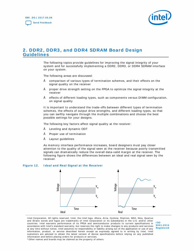
2. DDR2, DDR3, and DDR4 SDRAM Board DesignGuidelines
The following topics provide guidelines for improving the signal integrity of yoursystem and for successfully implementing a DDR2, DDR3, or DDR4 SDRAM interfaceon your system.
The following areas are discussed:
• comparison of various types of termination schemes, and their effects on thesignal quality on the receiver
• proper drive strength setting on the FPGA to optimize the signal integrity at thereceiver
• effects of different loading types, such as components versus DIMM configuration,on signal quality
It is important to understand the trade-offs between different types of terminationschemes, the effects of output drive strengths, and different loading types, so thatyou can swiftly navigate through the multiple combinations and choose the bestpossible settings for your designs.
The following key factors affect signal quality at the receiver:
• Leveling and dynamic ODT
• Proper use of termination
• Layout guidelines
As memory interface performance increases, board designers must pay closerattention to the quality of the signal seen at the receiver because poorly transmittedsignals can dramatically reduce the overall data-valid margin at the receiver. Thefollowing figure shows the differences between an ideal and real signal seen by thereceiver.
Figure 12. Ideal and Real Signal at the Receiver
Ideal Real
Volta
ge
Volta
geVIH VIH
VIL VIL
Time Time
EMI_DG | 2017.05.08
Send Feedback
Intel Corporation. All rights reserved. Intel, the Intel logo, Altera, Arria, Cyclone, Enpirion, MAX, Nios, Quartusand Stratix words and logos are trademarks of Intel Corporation or its subsidiaries in the U.S. and/or othercountries. Intel warrants performance of its FPGA and semiconductor products to current specifications inaccordance with Intel's standard warranty, but reserves the right to make changes to any products and servicesat any time without notice. Intel assumes no responsibility or liability arising out of the application or use of anyinformation, product, or service described herein except as expressly agreed to in writing by Intel. Intelcustomers are advised to obtain the latest version of device specifications before relying on any publishedinformation and before placing orders for products or services.*Other names and brands may be claimed as the property of others.
ISO9001:2015Registered
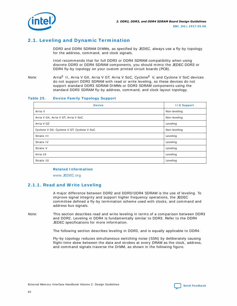
2.1. Leveling and Dynamic Termination
DDR3 and DDR4 SDRAM DIMMs, as specified by JEDEC, always use a fly-by topologyfor the address, command, and clock signals.
Intel recommends that for full DDR3 or DDR4 SDRAM compatibility when usingdiscrete DDR3 or DDR4 SDRAM components, you should mimic the JEDEC DDR3 orDDR4 fly-by topology on your custom printed circuit boards (PCB).
Note: Arria® II, Arria V GX, Arria V GT, Arria V SoC, Cyclone® V, and Cyclone V SoC devicesdo not support DDR3 SDRAM with read or write leveling, so these devices do notsupport standard DDR3 SDRAM DIMMs or DDR3 SDRAM components using thestandard DDR3 SDRAM fly-by address, command, and clock layout topology.
Table 25. Device Family Topology Support
Device I/O Support
Arria II Non-leveling
Arria V GX, Arria V GT, Arria V SoC Non-leveling
Arria V GZ Leveling
Cyclone V GX, Cyclone V GT, Cyclone V SoC Non-leveling
Stratix III Leveling
Stratix IV Leveling
Stratix V Leveling
Arria 10 Leveling
Stratix 10 Leveling
Related Information
www.JEDEC.org
2.1.1. Read and Write Leveling
A major difference between DDR2 and DDR3/DDR4 SDRAM is the use of leveling. Toimprove signal integrity and support higher frequency operations, the JEDECcommittee defined a fly-by termination scheme used with clocks, and command andaddress bus signals.
Note: This section describes read and write leveling in terms of a comparison between DDR3and DDR2. Leveling in DDR4 is fundamentally similar to DDR3. Refer to the DDR4JEDEC specifications for more information.
The following section describes leveling in DDR3, and is equally applicable to DDR4.
Fly-by topology reduces simultaneous switching noise (SSN) by deliberately causingflight-time skew between the data and strobes at every DRAM as the clock, address,and command signals traverse the DIMM, as shown in the following figure.
2. DDR2, DDR3, and DDR4 SDRAM Board Design Guidelines
EMI_DG | 2017.05.08
External Memory Interface Handbook Volume 2: Design Guidelines Send Feedback
82
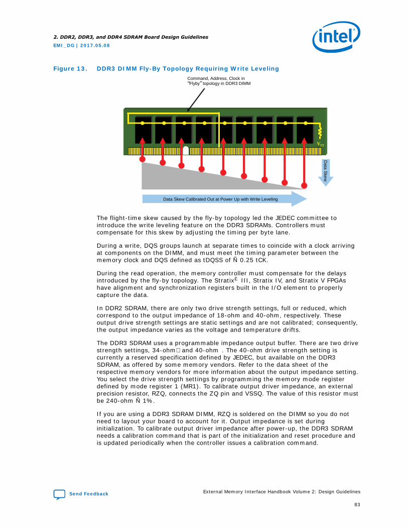
Figure 13. DDR3 DIMM Fly-By Topology Requiring Write Leveling
VTT
Data Skew Calibrated Out at Power Up with Write Leveling
Data S
kew
Command, Address, Clock in “Flyby” topology in DDR3 DIMM
The flight-time skew caused by the fly-by topology led the JEDEC committee tointroduce the write leveling feature on the DDR3 SDRAMs. Controllers mustcompensate for this skew by adjusting the timing per byte lane.
During a write, DQS groups launch at separate times to coincide with a clock arrivingat components on the DIMM, and must meet the timing parameter between thememory clock and DQS defined as tDQSS of ± 0.25 tCK.
During the read operation, the memory controller must compensate for the delaysintroduced by the fly-by topology. The Stratix® III, Stratix IV, and Stratix V FPGAshave alignment and synchronization registers built in the I/O element to properlycapture the data.
In DDR2 SDRAM, there are only two drive strength settings, full or reduced, whichcorrespond to the output impedance of 18-ohm and 40-ohm, respectively. Theseoutput drive strength settings are static settings and are not calibrated; consequently,the output impedance varies as the voltage and temperature drifts.
The DDR3 SDRAM uses a programmable impedance output buffer. There are two drivestrength settings, 34-ohmand 40-ohm . The 40-ohm drive strength setting iscurrently a reserved specification defined by JEDEC, but available on the DDR3SDRAM, as offered by some memory vendors. Refer to the data sheet of therespective memory vendors for more information about the output impedance setting.You select the drive strength settings by programming the memory mode registerdefined by mode register 1 (MR1). To calibrate output driver impedance, an externalprecision resistor, RZQ, connects the ZQ pin and VSSQ. The value of this resistor mustbe 240-ohm ± 1%.
If you are using a DDR3 SDRAM DIMM, RZQ is soldered on the DIMM so you do notneed to layout your board to account for it. Output impedance is set duringinitialization. To calibrate output driver impedance after power-up, the DDR3 SDRAMneeds a calibration command that is part of the initialization and reset procedure andis updated periodically when the controller issues a calibration command.
2. DDR2, DDR3, and DDR4 SDRAM Board Design Guidelines
EMI_DG | 2017.05.08
Send Feedback External Memory Interface Handbook Volume 2: Design Guidelines
83
In addition to calibrated output impedance, the DDR3 SDRAM also supports calibratedparallel ODT through the same external precision resistor, RZQ, which is possible byusing a merged output driver structure in the DDR3 SDRAM, which also helps toimprove pin capacitance in the DQ and DQS pins. The ODT values supported in DDR3SDRAM are 20-ohm , 30-ohm , 40-ohm , 60-ohm , and 120-ohm , assuming that RZQis 240-ohm.
Related Information
www.JEDEC.org
2.1.2. Dynamic ODT
Dynamic ODT is a feature in DDR3 and DDR4 SDRAM that is not available in DDR2SDRAM. Dynamic ODT can change the ODT setting without issuing a mode register set(MRS) command.
Note: This topic highlights the dynamic ODT feature in DDR3. To learn about dynamic ODT inDDR4, refer to the JEDEC DDR4 specifications.
When you enable dynamic ODT, and there is no write operation, the DDR3 SDRAMterminates to a termination setting of RTT_NOM; when there is a write operation, theDDR3 SDRAM terminates to a setting of RTT_WR. You can preset the values ofRTT_NOM and RTT_WR by programming the mode registers, MR1 and MR2.
The following figure shows the behavior of ODT when you enable dynamic ODT.
Figure 14. Dynamic ODT: Behavior with ODT Asserted Before and After the Write
In the multi-load DDR3 SDRAM configuration, dynamic ODT helps reduce the jitter atthe module being accessed, and minimizes reflections from any secondary modules.
For more information about using the dynamic ODT on DDR3 SDRAM, refer to theapplication note by Micron, TN-41-04 DDR3 Dynamic On-Die Termination.
In addition to RTT_NOM and RTT_WR, DDR4 has RTT_PARK which applies a specifiedtermination value when the ODT signal is low.
Related Information
www.JEDEC.org
2.1.3. Dynamic On-Chip Termination
Dynamic OCT is available in Arria V, Arria 10, Cyclone V, Stratix III, Stratix IV,Stratix V, and Stratix 10.
2. DDR2, DDR3, and DDR4 SDRAM Board Design Guidelines
EMI_DG | 2017.05.08
External Memory Interface Handbook Volume 2: Design Guidelines Send Feedback
84
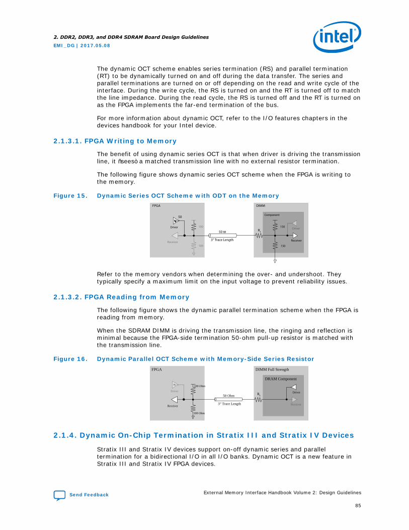
The dynamic OCT scheme enables series termination (RS) and parallel termination(RT) to be dynamically turned on and off during the data transfer. The series andparallel terminations are turned on or off depending on the read and write cycle of theinterface. During the write cycle, the RS is turned on and the RT is turned off to matchthe line impedance. During the read cycle, the RS is turned off and the RT is turned onas the FPGA implements the far-end termination of the bus.
For more information about dynamic OCT, refer to the I/O features chapters in thedevices handbook for your Intel device.
2.1.3.1. FPGA Writing to Memory
The benefit of using dynamic series OCT is that when driver is driving the transmissionline, it “sees” a matched transmission line with no external resistor termination.
The following figure shows dynamic series OCT scheme when the FPGA is writing tothe memory.
Figure 15. Dynamic Series OCT Scheme with ODT on the MemoryFPGA DIMM
Component
RS Driver Driver
Receiver
50 w
3” Trace Length Receiver
50
150
150
100
100
Refer to the memory vendors when determining the over- and undershoot. Theytypically specify a maximum limit on the input voltage to prevent reliability issues.
2.1.3.2. FPGA Reading from Memory
The following figure shows the dynamic parallel termination scheme when the FPGA isreading from memory.
When the SDRAM DIMM is driving the transmission line, the ringing and reflection isminimal because the FPGA-side termination 50-ohm pull-up resistor is matched withthe transmission line.
Figure 16. Dynamic Parallel OCT Scheme with Memory-Side Series ResistorFPGA DIMM Full Strength
DRAM Component
RS
Driver Driver
Receiver
50 Ohm
3” Trace Length Receiver
100 Ohm
100 Ohm
2.1.4. Dynamic On-Chip Termination in Stratix III and Stratix IV Devices
Stratix III and Stratix IV devices support on-off dynamic series and paralleltermination for a bidirectional I/O in all I/O banks. Dynamic OCT is a new feature inStratix III and Stratix IV FPGA devices.
2. DDR2, DDR3, and DDR4 SDRAM Board Design Guidelines
EMI_DG | 2017.05.08
Send Feedback External Memory Interface Handbook Volume 2: Design Guidelines
85
You enable dynamic parallel termination only when the bidirectional I/O acts as areceiver and disable it when the bidirectional I/O acts as a driver. Similarly, you enabledynamic series termination only when the bidirectional I/O acts as a driver and isdisable it when the bidirectional I/O acts as a receiver. The default setting for dynamicOCT is series termination, to save power when the interface is idle—no active reads orwrites.
Note: The dynamic control operation of the OCT is separate to the output enable signal forthe buffer. UniPHY IP can enable parallel OCT only during read cycles, saving powerwhen the interface is idle.
Figure 17. Dynamic OCT Between Stratix III and Stratix IV FPGA Devices
Drive r
Re ce ive r
Drive r
Re ce ive r
0 Ω
VREF = 0.75 V
DDR3 DIMMFPG A
50
3" Tra ce Le ngth
DDR3 Comp one nt
R S = 15 Ω
34 W
100 W
100 W
VREF = 0.75 V
Drive r
Re ce ive r
Drive r
Re ce ive r
VREF = 0.75 V
DDR3 DIMMFPG A
50 W
3" Tra ce Le ngth
DDR3 Comp one nt
R S = 15 Ω
34 Ω
100 Ω
100 ΩVREF = 0.75 V
0 Ω
Ω
Dynamic OCT is useful for terminating any high-performance bidirectional pathbecause signal integrity is optimized depending on the direction of the data. Inaddition, dynamic OCT also eliminates the need for external termination resistorswhen used with memory devices that support ODT (such as DDR3 SDRAM), thusreducing cost and easing board layout.
However, dynamic OCT in Stratix III and Stratix IV FPGA devices is different fromdynamic ODT in DDR3 SDRAM mentioned in previous sections and these featuresshould not be assumed to be identical.
For detailed information about the dynamic OCT feature in the Stratix III FPGA, referto the Stratix III Device I/O Features chapter in volume 1 of the Stratix III DeviceHandbook.
For detailed information about the dynamic OCT feature in the Stratix IV FPGA, referto the I/O Features in Stratix IV Devices chapter in volume 1 of the Stratix IV DeviceHandbook.
Related Information
• Stratix III Device I/O Features
• I/O Features in Stratix IV Devices
2. DDR2, DDR3, and DDR4 SDRAM Board Design Guidelines
EMI_DG | 2017.05.08
External Memory Interface Handbook Volume 2: Design Guidelines Send Feedback
86
2.1.5. Dynamic OCT in Stratix V Devices
Stratix V devices also support the dynamic OCT feature and provide more flexibility.Stratix V OCT calibration uses one RZQ pin that exists in every OCT block.
You can use any one of the following as a reference resistor on the RZQ pin toimplement different OCT values:
• 240-ohm reference resistor—to implement RS OCT of 34-ohm, 40-ohm, 48-ohm,60-ohm, and 80-ohm; and RT OCT resistance of 20-ohm, 30-ohm, 40-ohm, and120-ohm
• 100-ohm reference resistor—to implement RS OCT of 25-ohm and 50-ohm; andRT OCT resistance of 50-ohm
For detailed information about the dynamic OCT feature in the Stratix V FPGA, refer tothe I/O Features in Stratix V Devices chapter in volume 1 of the Stratix V DeviceHandbook.
Related Information
I/O Features in Stratix V Devices
2.1.6. Dynamic On-Chip Termination (OCT) in Arria 10 and Stratix 10Devices
Depending upon the Rs (series) and Rt (parallel) OCT values that you want, youshould choose appropriate values for the RZQ resistor and connect this resistor to theRZQ pin of the FPGA.
• Select a 240-ohm reference resistor to ground to implement Rs OCT values of 34-ohm, 40-ohm, 48-ohm, 60-ohm, and 80-ohm, and Rt OCT resistance values of 20-ohm, 30-ohm, 34-ohm, 40-ohm, 60-ohm, 80-ohm, 120-ohm and 240 ohm.
• Select a 100-ohm reference resistor to ground to implement Rs OCT values of 25-ohm and 50-ohm, and an RT OCT resistance of 50-ohm.
Check the FPGA I/O tab of the parameter editor to determine the I/O standards andtermination values supported for data, address and command, and memory clocksignals.
2.2. DDR2 Terminations and Guidelines
This section provides information for DDR2 SDRAM interfaces.
2.2.1. Termination for DDR2 SDRAM
DDR2 adheres to the JEDEC standard of governing Stub-Series Terminated Logic(SSTL), JESD8-15a, which includes four different termination schemes.
Two commonly used termination schemes of SSTL are:
• Single parallel terminated output load with or without series resistors (Class I, asstated in JESD8-15a)
• Double parallel terminated output load with or without series resistors (Class II, asstated in JESD8-15a)
2. DDR2, DDR3, and DDR4 SDRAM Board Design Guidelines
EMI_DG | 2017.05.08
Send Feedback External Memory Interface Handbook Volume 2: Design Guidelines
87
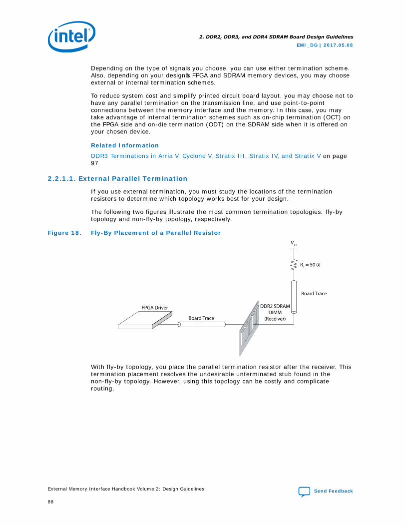
Depending on the type of signals you choose, you can use either termination scheme.Also, depending on your design’s FPGA and SDRAM memory devices, you may chooseexternal or internal termination schemes.
To reduce system cost and simplify printed circuit board layout, you may choose not tohave any parallel termination on the transmission line, and use point-to-pointconnections between the memory interface and the memory. In this case, you maytake advantage of internal termination schemes such as on-chip termination (OCT) onthe FPGA side and on-die termination (ODT) on the SDRAM side when it is offered onyour chosen device.
Related Information
DDR3 Terminations in Arria V, Cyclone V, Stratix III, Stratix IV, and Stratix V on page97
2.2.1.1. External Parallel Termination
If you use external termination, you must study the locations of the terminationresistors to determine which topology works best for your design.
The following two figures illustrate the most common termination topologies: fly-bytopology and non-fly-by topology, respectively.
Figure 18. Fly-By Placement of a Parallel Resistor
FPGA Driver
Board Trace
DDR2 SDRAMDIMM
(Receiver)
Board Trace
RT = 50 w
VTT
With fly-by topology, you place the parallel termination resistor after the receiver. Thistermination placement resolves the undesirable unterminated stub found in thenon-fly-by topology. However, using this topology can be costly and complicaterouting.
2. DDR2, DDR3, and DDR4 SDRAM Board Design Guidelines
EMI_DG | 2017.05.08
External Memory Interface Handbook Volume 2: Design Guidelines Send Feedback
88
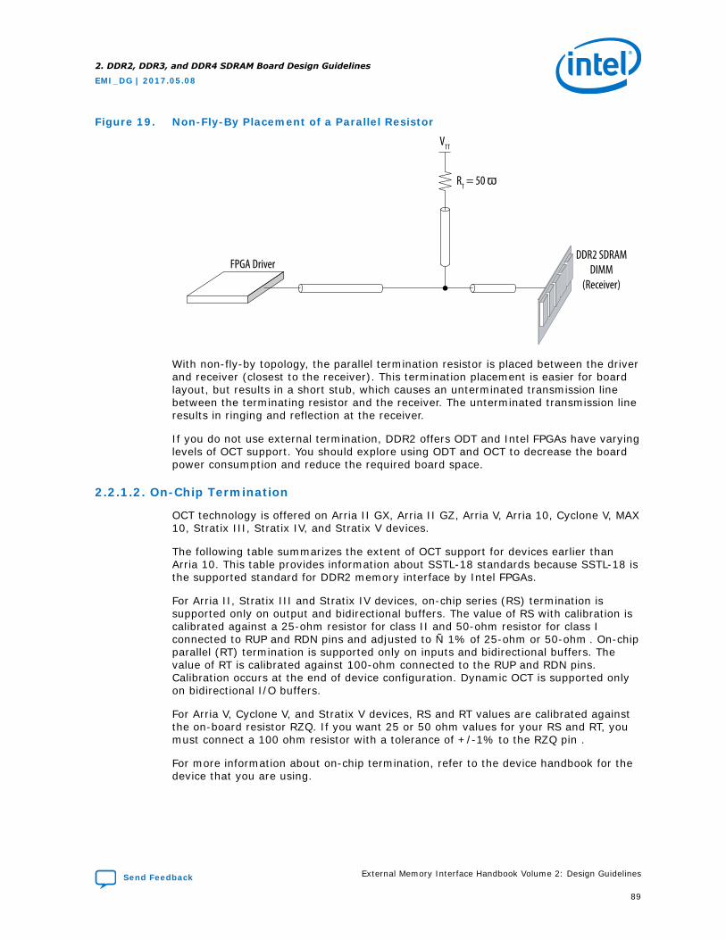
Figure 19. Non-Fly-By Placement of a Parallel Resistor
FPGA DriverDDR2 SDRAM
DIMM(Receiver)
RT = 50 w
VTT
With non-fly-by topology, the parallel termination resistor is placed between the driverand receiver (closest to the receiver). This termination placement is easier for boardlayout, but results in a short stub, which causes an unterminated transmission linebetween the terminating resistor and the receiver. The unterminated transmission lineresults in ringing and reflection at the receiver.
If you do not use external termination, DDR2 offers ODT and Intel FPGAs have varyinglevels of OCT support. You should explore using ODT and OCT to decrease the boardpower consumption and reduce the required board space.
2.2.1.2. On-Chip Termination
OCT technology is offered on Arria II GX, Arria II GZ, Arria V, Arria 10, Cyclone V, MAX10, Stratix III, Stratix IV, and Stratix V devices.
The following table summarizes the extent of OCT support for devices earlier thanArria 10. This table provides information about SSTL-18 standards because SSTL-18 isthe supported standard for DDR2 memory interface by Intel FPGAs.
For Arria II, Stratix III and Stratix IV devices, on-chip series (RS) termination issupported only on output and bidirectional buffers. The value of RS with calibration iscalibrated against a 25-ohm resistor for class II and 50-ohm resistor for class Iconnected to RUP and RDN pins and adjusted to ± 1% of 25-ohm or 50-ohm . On-chipparallel (RT) termination is supported only on inputs and bidirectional buffers. Thevalue of RT is calibrated against 100-ohm connected to the RUP and RDN pins.Calibration occurs at the end of device configuration. Dynamic OCT is supported onlyon bidirectional I/O buffers.
For Arria V, Cyclone V, and Stratix V devices, RS and RT values are calibrated againstthe on-board resistor RZQ. If you want 25 or 50 ohm values for your RS and RT, youmust connect a 100 ohm resistor with a tolerance of +/-1% to the RZQ pin .
For more information about on-chip termination, refer to the device handbook for thedevice that you are using.
2. DDR2, DDR3, and DDR4 SDRAM Board Design Guidelines
EMI_DG | 2017.05.08
Send Feedback External Memory Interface Handbook Volume 2: Design Guidelines
89
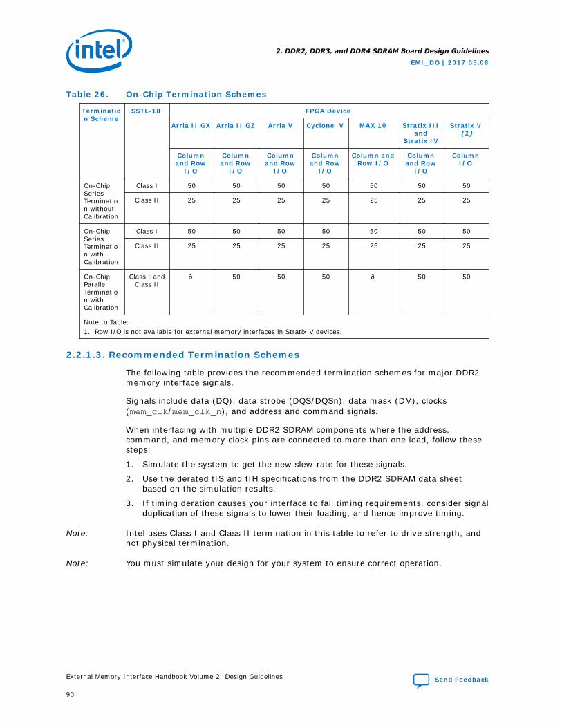
Table 26. On-Chip Termination Schemes
Termination Scheme
SSTL-18 FPGA Device
Arria II GX Arria II GZ Arria V Cyclone V MAX 10 Stratix IIIand
Stratix IV
Stratix V (1)
Columnand Row
I/O
Columnand Row
I/O
Columnand Row
I/O
Columnand Row
I/O
Column andRow I/O
Columnand Row
I/O
ColumnI/O
On-ChipSeriesTermination withoutCalibration
Class I 50 50 50 50 50 50 50
Class II 25 25 25 25 25 25 25
On-ChipSeriesTermination withCalibration
Class I 50 50 50 50 50 50 50
Class II 25 25 25 25 25 25 25
On-ChipParallelTermination withCalibration
Class I andClass II
— 50 50 50 — 50 50
Note to Table:1. Row I/O is not available for external memory interfaces in Stratix V devices.
2.2.1.3. Recommended Termination Schemes
The following table provides the recommended termination schemes for major DDR2memory interface signals.
Signals include data (DQ), data strobe (DQS/DQSn), data mask (DM), clocks(mem_clk/mem_clk_n), and address and command signals.
When interfacing with multiple DDR2 SDRAM components where the address,command, and memory clock pins are connected to more than one load, follow thesesteps:
1. Simulate the system to get the new slew-rate for these signals.
2. Use the derated tIS and tIH specifications from the DDR2 SDRAM data sheetbased on the simulation results.
3. If timing deration causes your interface to fail timing requirements, consider signalduplication of these signals to lower their loading, and hence improve timing.
Note: Intel uses Class I and Class II termination in this table to refer to drive strength, andnot physical termination.
Note: You must simulate your design for your system to ensure correct operation.
2. DDR2, DDR3, and DDR4 SDRAM Board Design Guidelines
EMI_DG | 2017.05.08
External Memory Interface Handbook Volume 2: Design Guidelines Send Feedback
90
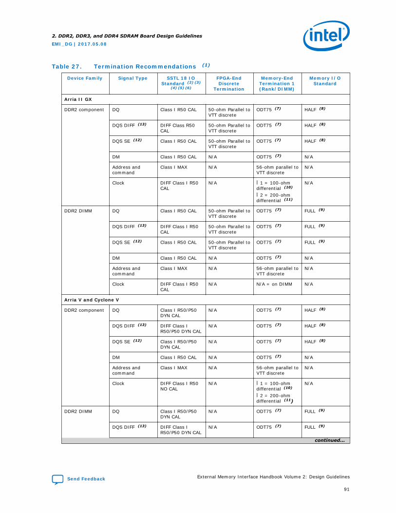
Table 27. Termination Recommendations (1)
Device Family Signal Type SSTL 18 IOStandard (2) (3)
(4) (5) (6)
FPGA-EndDiscrete
Termination
Memory-EndTermination 1(Rank/DIMM)
Memory I/OStandard
Arria II GX
DDR2 component DQ Class I R50 CAL 50-ohm Parallel toVTT discrete
ODT75 (7) HALF (8)
DQS DIFF (13) DIFF Class R50CAL
50-ohm Parallel toVTT discrete
ODT75 (7) HALF (8)
DQS SE (12) Class I R50 CAL 50-ohm Parallel toVTT discrete
ODT75 (7) HALF (8)
DM Class I R50 CAL N/A ODT75 (7) N/A
Address andcommand
Class I MAX N/A 56-ohm parallel toVTT discrete
N/A
Clock DIFF Class I R50CAL
N/A ×1 = 100-ohmdifferential (10)
×2 = 200-ohmdifferential (11)
N/A
DDR2 DIMM DQ Class I R50 CAL 50-ohm Parallel toVTT discrete
ODT75 (7) FULL (9)
DQS DIFF (13) DIFF Class I R50CAL
50-ohm Parallel toVTT discrete
ODT75 (7) FULL (9)
DQS SE (12) Class I R50 CAL 50-ohm Parallel toVTT discrete
ODT75 (7) FULL (9)
DM Class I R50 CAL N/A ODT75 (7) N/A
Address andcommand
Class I MAX N/A 56-ohm parallel toVTT discrete
N/A
Clock DIFF Class I R50CAL
N/A N/A = on DIMM N/A
Arria V and Cyclone V
DDR2 component DQ Class I R50/P50DYN CAL
N/A ODT75 (7) HALF (8)
DQS DIFF (13) DIFF Class IR50/P50 DYN CAL
N/A ODT75 (7) HALF (8)
DQS SE (12) Class I R50/P50DYN CAL
N/A ODT75 (7) HALF (8)
DM Class I R50 CAL N/A ODT75 (7) N/A
Address andcommand
Class I MAX N/A 56-ohm parallel toVTT discrete
N/A
Clock DIFF Class I R50NO CAL
N/A ×1 = 100-ohmdifferential (10)
×2 = 200-ohmdifferential (11)
N/A
DDR2 DIMM DQ Class I R50/P50DYN CAL
N/A ODT75 (7) FULL (9)
DQS DIFF (13) DIFF Class IR50/P50 DYN CAL
N/A ODT75 (7) FULL (9)
continued...
2. DDR2, DDR3, and DDR4 SDRAM Board Design Guidelines
EMI_DG | 2017.05.08
Send Feedback External Memory Interface Handbook Volume 2: Design Guidelines
91
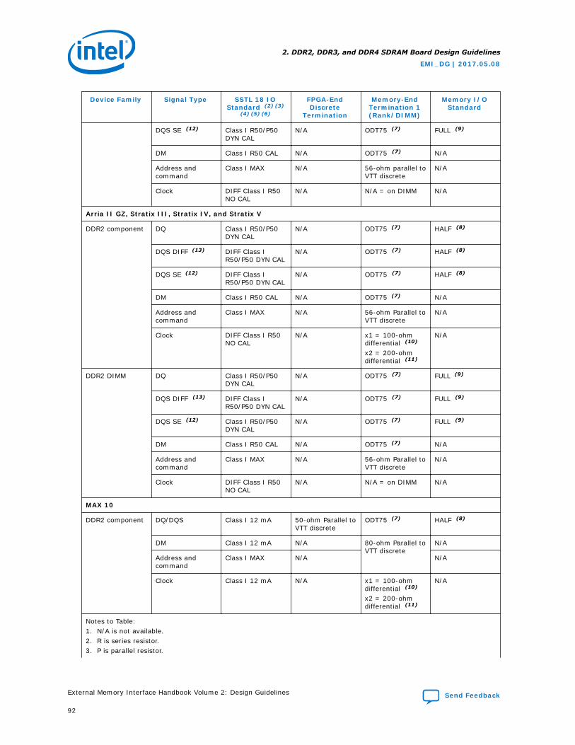
Device Family Signal Type SSTL 18 IOStandard (2) (3)
(4) (5) (6)
FPGA-EndDiscrete
Termination
Memory-EndTermination 1(Rank/DIMM)
Memory I/OStandard
DQS SE (12) Class I R50/P50DYN CAL
N/A ODT75 (7) FULL (9)
DM Class I R50 CAL N/A ODT75 (7) N/A
Address andcommand
Class I MAX N/A 56-ohm parallel toVTT discrete
N/A
Clock DIFF Class I R50NO CAL
N/A N/A = on DIMM N/A
Arria II GZ, Stratix III, Stratix IV, and Stratix V
DDR2 component DQ Class I R50/P50DYN CAL
N/A ODT75 (7) HALF (8)
DQS DIFF (13) DIFF Class IR50/P50 DYN CAL
N/A ODT75 (7) HALF (8)
DQS SE (12) DIFF Class IR50/P50 DYN CAL
N/A ODT75 (7) HALF (8)
DM Class I R50 CAL N/A ODT75 (7) N/A
Address andcommand
Class I MAX N/A 56-ohm Parallel toVTT discrete
N/A
Clock DIFF Class I R50NO CAL
N/A x1 = 100-ohmdifferential (10)
x2 = 200-ohmdifferential (11)
N/A
DDR2 DIMM DQ Class I R50/P50DYN CAL
N/A ODT75 (7) FULL (9)
DQS DIFF (13) DIFF Class IR50/P50 DYN CAL
N/A ODT75 (7) FULL (9)
DQS SE (12) Class I R50/P50DYN CAL
N/A ODT75 (7) FULL (9)
DM Class I R50 CAL N/A ODT75 (7) N/A
Address andcommand
Class I MAX N/A 56-ohm Parallel toVTT discrete
N/A
Clock DIFF Class I R50NO CAL
N/A N/A = on DIMM N/A
MAX 10
DDR2 component DQ/DQS Class I 12 mA 50-ohm Parallel toVTT discrete
ODT75 (7) HALF (8)
DM Class I 12 mA N/A 80-ohm Parallel toVTT discrete
N/A
Address andcommand
Class I MAX N/A N/A
Clock Class I 12 mA N/A x1 = 100-ohmdifferential (10)
x2 = 200-ohmdifferential (11)
N/A
Notes to Table:1. N/A is not available.2. R is series resistor.3. P is parallel resistor.
2. DDR2, DDR3, and DDR4 SDRAM Board Design Guidelines
EMI_DG | 2017.05.08
External Memory Interface Handbook Volume 2: Design Guidelines Send Feedback
92
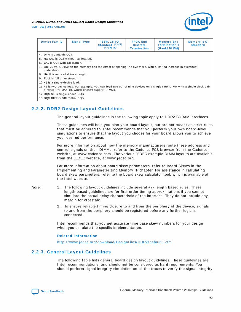
Device Family Signal Type SSTL 18 IOStandard (2) (3)
(4) (5) (6)
FPGA-EndDiscrete
Termination
Memory-EndTermination 1(Rank/DIMM)
Memory I/OStandard
4. DYN is dynamic OCT.5. NO CAL is OCT without calibration.6. CAL is OCT with calibration.7. ODT75 vs. ODT50 on the memory has the effect of opening the eye more, with a limited increase in overshoot/
undershoot.8. HALF is reduced drive strength.9. FULL is full drive strength.10.x1 is a single-device load.11.x2 is two-device load. For example, you can feed two out of nine devices on a single rank DIMM with a single clock pair
—except for MAX 10, which doesn't support DIMMs.12.DQS SE is single-ended DQS.13.DQS DIFF is differential DQS
2.2.2. DDR2 Design Layout Guidelines
The general layout guidelines in the following topic apply to DDR2 SDRAM interfaces.
These guidelines will help you plan your board layout, but are not meant as strict rulesthat must be adhered to. Intel recommends that you perform your own board-levelsimulations to ensure that the layout you choose for your board allows you to achieveyour desired performance.
For more information about how the memory manufacturers route these address andcontrol signals on their DIMMs, refer to the Cadence PCB browser from the Cadencewebsite, at www.cadence.com. The various JEDEC example DIMM layouts are availablefrom the JEDEC website, at www.jedec.org.
For more information about board skew parameters, refer to Board Skews in theImplementing and Parameterizing Memory IP chapter. For assistance in calculatingboard skew parameters, refer to the board skew calculator tool, which is available atthe Intel website.
Note: 1. The following layout guidelines include several +/- length based rules. Theselength based guidelines are for first order timing approximations if you cannotsimulate the actual delay characteristic of the interface. They do not include anymargin for crosstalk.
2. To ensure reliable timing closure to and from the periphery of the device, signalsto and from the periphery should be registered before any further logic isconnected.
Intel recommends that you get accurate time base skew numbers for your designwhen you simulate the specific implementation.
Related Information
http://www.jedec.org/download/DesignFiles/DDR2/default1.cfm
2.2.3. General Layout Guidelines
The following table lists general board design layout guidelines. These guidelines areIntel recommendations, and should not be considered as hard requirements. Youshould perform signal integrity simulation on all the traces to verify the signal integrity
2. DDR2, DDR3, and DDR4 SDRAM Board Design Guidelines
EMI_DG | 2017.05.08
Send Feedback External Memory Interface Handbook Volume 2: Design Guidelines
93
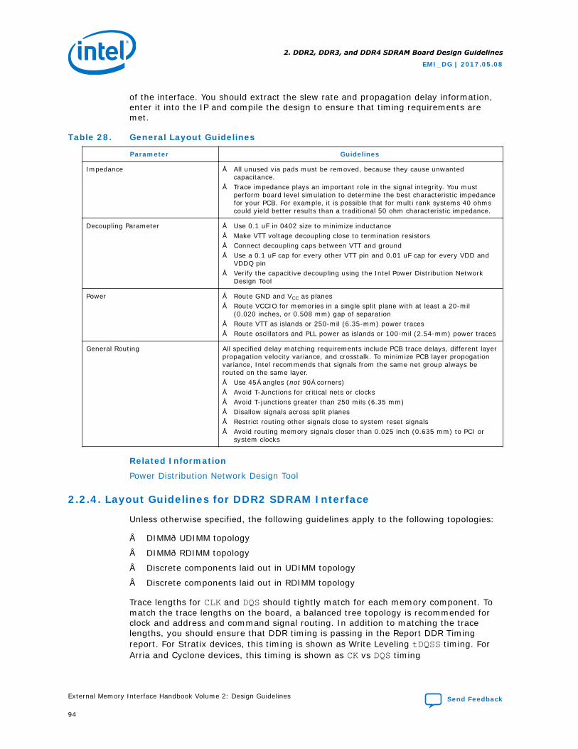
of the interface. You should extract the slew rate and propagation delay information,enter it into the IP and compile the design to ensure that timing requirements aremet.
Table 28. General Layout Guidelines
Parameter Guidelines
Impedance • All unused via pads must be removed, because they cause unwantedcapacitance.
• Trace impedance plays an important role in the signal integrity. You mustperform board level simulation to determine the best characteristic impedancefor your PCB. For example, it is possible that for multi rank systems 40 ohmscould yield better results than a traditional 50 ohm characteristic impedance.
Decoupling Parameter • Use 0.1 uF in 0402 size to minimize inductance• Make VTT voltage decoupling close to termination resistors• Connect decoupling caps between VTT and ground• Use a 0.1 uF cap for every other VTT pin and 0.01 uF cap for every VDD and
VDDQ pin• Verify the capacitive decoupling using the Intel Power Distribution Network
Design Tool
Power • Route GND and VCC as planes• Route VCCIO for memories in a single split plane with at least a 20-mil
(0.020 inches, or 0.508 mm) gap of separation• Route VTT as islands or 250-mil (6.35-mm) power traces• Route oscillators and PLL power as islands or 100-mil (2.54-mm) power traces
General Routing All specified delay matching requirements include PCB trace delays, different layerpropagation velocity variance, and crosstalk. To minimize PCB layer propogationvariance, Intel recommends that signals from the same net group always berouted on the same layer.• Use 45° angles (not 90° corners)• Avoid T-Junctions for critical nets or clocks• Avoid T-junctions greater than 250 mils (6.35 mm)• Disallow signals across split planes• Restrict routing other signals close to system reset signals• Avoid routing memory signals closer than 0.025 inch (0.635 mm) to PCI or
system clocks
Related Information
Power Distribution Network Design Tool
2.2.4. Layout Guidelines for DDR2 SDRAM Interface
Unless otherwise specified, the following guidelines apply to the following topologies:
• DIMM—UDIMM topology
• DIMM—RDIMM topology
• Discrete components laid out in UDIMM topology
• Discrete components laid out in RDIMM topology
Trace lengths for CLK and DQS should tightly match for each memory component. Tomatch the trace lengths on the board, a balanced tree topology is recommended forclock and address and command signal routing. In addition to matching the tracelengths, you should ensure that DDR timing is passing in the Report DDR Timingreport. For Stratix devices, this timing is shown as Write Leveling tDQSS timing. ForArria and Cyclone devices, this timing is shown as CK vs DQS timing
2. DDR2, DDR3, and DDR4 SDRAM Board Design Guidelines
EMI_DG | 2017.05.08
External Memory Interface Handbook Volume 2: Design Guidelines Send Feedback
94
For a table of device family topology support, refer to Leveling and Dynamic ODT.
The following table lists DDR2 SDRAM layout guidelines. These guidelines are Intelrecommendations, and should not be considered as hard requirements. You shouldperform signal integrity simulation on all the traces to verify the signal integrity of theinterface. You should extract the slew rate and propagation delay information, enter itinto the IP and compile the design to ensure that timing requirements are met.
Note: The following layout guidelines also apply to DDR3 SDRAM without leveling interfaces.
Table 29. DDR2 SDRAM Layout Guidelines (1)
Parameter Guidelines
DIMMs If you consider a normal DDR2 unbuffered, unregistered DIMM, essentially you areplanning to perform the DIMM routing directly on your PCB. Therefore, eachaddress and control pin routes from the FPGA (single pin) to all memory devicesmust be on the same side of the FPGA.
General Routing • All data, address, and command signals must have matched length traces± 50 ps.
• All signals within a given Byte Lane Group should be matched length withmaximum deviation of ±10 ps and routed in the same layer.
Clock Routing • A 4.7 K-ohm resistor to ground is recommended for each Clock Enable signal.You can place the resistor at either the memory end or the FPGA end of thetrace.
• Route clocks on inner layers with outer-layer run lengths held to under 500mils (12.7 mm)
• These signals should maintain a10-mil (0.254 mm) spacing from other nets• Clocks should maintain a length-matching between clock pairs of ±5 ps.• Differential clocks should maintain a length-matching between P and N signals
of ±2 ps, routed in parallel.• Space between different pairs should be at least three times the space
between the differential pairs and must be routed differentially (5-mil trace,10-15 mil space on centers), and equal to the signals in the Address/Command Group or up to 100 mils (2.54 mm) longer than the signals in theAddress/Command Group.
• Trace lengths for CLK and DQS should closely match for each memorycomponent. To match trace lengths on the board, a balanced tree topology isrecommended for clock and address and command signal routing. For Stratixdevice families, ensure that Write Leveling tDQSS is passing in the DDR timingreport; for Arria and Cyclone device families, verify that CK vs DQS timing ispassing in the DDR timing report.
Address and Command Routing • Unbuffered address and command lines are more susceptible to cross-talk andare generally noisier than buffered address or command lines. Therefore,un-buffered address and command signals should be routed on a differentlayer than data signals (DQ) and data mask signals (DM) and with greaterspacing.
• Do not route differential clock (CK) and clock enable (CKE) signals close toaddress signals.
continued...
2. DDR2, DDR3, and DDR4 SDRAM Board Design Guidelines
EMI_DG | 2017.05.08
Send Feedback External Memory Interface Handbook Volume 2: Design Guidelines
95
Parameter Guidelines
DQ, DM, and DQS Routing Rules • Keep the distance from the pin on the DDR2 DIMM or component to thetermination resistor pack (VTT) to less than 500 mils for DQS[x] Data Groups.
• Keep the distance from the pin on the DDR2 DIMM or component to thetermination resistor pack (VTT) to less than 1000 mils for the ADR_CMD_CTLAddress Group.
• Parallelism rules for the DQS[x] Data Groups are as follows:— 4 mils for parallel runs < 0.1 inch (approximately 1× spacing relative to
plane distance)— 5 mils for parallel runs < 0.5 inch (approximately 1× spacing relative to
plane distance)— 10 mils for parallel runs between 0.5 and 1.0 inches (approximately 2×
spacing relative to plane distance)— 15 mils for parallel runs between 1.0 and 6.0 inch (approximately 3×
spacing relative to plane distance)• Parallelism rules for the ADR_CMD_CTL group and CLOCKS group are as
follows:— 4 mils for parallel runs < 0.1 inch (approximately 1× spacing relative to
plane distance)— 10 mils for parallel runs < 0.5 inch (approximately 2× spacing relative to
plane distance)— 15 mils for parallel runs between 0.5 and 1.0 inches (approximately 3×
spacing relative to plane distance)— 20 mils for parallel runs between 1.0 and 6.0 inches (approximately 4×
spacing relative to plane distance)• All signals are to maintain a 20-mil separation from other, non-related nets.• All signals must have a total length of < 6 inches.• Trace lengths for CLK and DQS should closely match for each memory
component. To match trace lengths on the board, a balanced tree topology isrecommended for clock and address and command signal routing. For Stratixdevice families, ensure that Write Leveling tDQSS is passing in the DDR timingreport; for Arria and Cyclone device families, verify that CK vs DQS timing ispassing in the DDR timing report.
Termination Rules • When pull-up resistors are used, fly-by termination configuration isrecommended. Fly-by helps reduce stub reflection issues.
• Pull-ups should be within 0.5 to no more than 1 inch.• Pull up is typically 56-ohms.• If using resistor networks:• Do not share R-pack series resistors between address/command and data lines
(DQ, DQS, and DM) to eliminate crosstalk within pack.• Series and pull up tolerances are 1–2%.• Series resistors are typically 10 to 20-ohm.• Address and control series resistor typically at the FPGA end of the link.• DM, DQS, DQ series resistor typically at the memory end of the link (or just
before the first DIMM).
continued...
2. DDR2, DDR3, and DDR4 SDRAM Board Design Guidelines
EMI_DG | 2017.05.08
External Memory Interface Handbook Volume 2: Design Guidelines Send Feedback
96
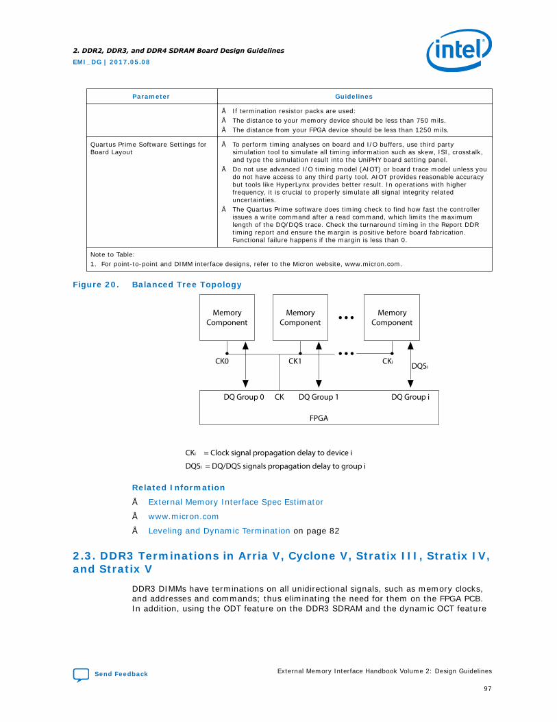
Parameter Guidelines
• If termination resistor packs are used:• The distance to your memory device should be less than 750 mils.• The distance from your FPGA device should be less than 1250 mils.
Quartus Prime Software Settings forBoard Layout
• To perform timing analyses on board and I/O buffers, use third partysimulation tool to simulate all timing information such as skew, ISI, crosstalk,and type the simulation result into the UniPHY board setting panel.
• Do not use advanced I/O timing model (AIOT) or board trace model unless youdo not have access to any third party tool. AIOT provides reasonable accuracybut tools like HyperLynx provides better result. In operations with higherfrequency, it is crucial to properly simulate all signal integrity relateduncertainties.
• The Quartus Prime software does timing check to find how fast the controllerissues a write command after a read command, which limits the maximumlength of the DQ/DQS trace. Check the turnaround timing in the Report DDRtiming report and ensure the margin is positive before board fabrication.Functional failure happens if the margin is less than 0.
Note to Table:1. For point-to-point and DIMM interface designs, refer to the Micron website, www.micron.com.
Figure 20. Balanced Tree Topology
MemoryComponent
MemoryComponent
MemoryComponent
DQ Group 0
CK0 CK1 DQSiCKi
CKi = Clock signal propagation delay to device i
DQSi = DQ/DQS signals propagation delay to group i
FPGA
DQ Group 1 DQ Group iCK
Related Information
• External Memory Interface Spec Estimator
• www.micron.com
• Leveling and Dynamic Termination on page 82
2.3. DDR3 Terminations in Arria V, Cyclone V, Stratix III, Stratix IV,and Stratix V
DDR3 DIMMs have terminations on all unidirectional signals, such as memory clocks,and addresses and commands; thus eliminating the need for them on the FPGA PCB.In addition, using the ODT feature on the DDR3 SDRAM and the dynamic OCT feature
2. DDR2, DDR3, and DDR4 SDRAM Board Design Guidelines
EMI_DG | 2017.05.08
Send Feedback External Memory Interface Handbook Volume 2: Design Guidelines
97
of Stratix III, Stratix IV, and Stratix V FPGAs completely eliminates any externaltermination resistors; thus simplifying the layout for the DDR3 SDRAM interface whencompared to that of the DDR2 SDRAM interface.
The following topics describe the correct way to terminate a DDR3 SDRAM interfacetogether with Stratix III, Stratix IV, and Stratix V FPGA devices.
Note: If you are using a DDR3 SDRAM without leveling interface, refer to “Board Terminationfor DDR2 SDRAM”. Note also that Arria V and Cyclone V devices do not support DDR3with leveling.
Related Information
Termination for DDR2 SDRAM on page 87
2.3.1. Terminations for Single-Rank DDR3 SDRAM Unbuffered DIMM
The most common implementation of the DDR3 SDRAM interface is the unbufferedDIMM (UDIMM). You can find DDR3 SDRAM UDIMMs in many applications, especially inPC applications.
The following table lists the recommended termination and drive strength setting forUDIMM and Stratix III, Stratix IV, and Stratix V FPGA devices.
Note: These settings are just recommendations for you to get started. Simulate with realboard and try different settings to get the best SI.
Table 30. Drive Strength and ODT Setting Recommendations for Single-Rank UDIMM
Signal Type SSTL 15 I/OStandard (1)
FPGA End On-BoardTermination (2)
Memory EndTermination for
Write
Memory DriverStrength for Read
DQ Class I R50C/G50C (3)
— 60-ohm ODT (4) 40-ohm (4)
DQS Differential Class IR50C/G50C (3)
— 60-ohm ODT (4) 40-ohm (4)
DM Class I R50C (3) — 60-ohm ODT (4) 40-ohm (4)
Address andCommand
Class I with maximumdrive strength
— 39-ohm on-board termination to VDD (5)
CK/CK# Differential Class IR50C
— On-board (5)
2.2 pf compensation cap before the firstcomponent; 36-ohm termination to VDD foreach arm (72-ohm differential); add 0.1 uF justbefore VDD.
Notes to Table:1. UniPHY IP automatically implements these settings.2. Intel recommends that you use dynamic on-chip termination (OCT) for Stratix III and Stratix IV device families.3. R50C is series with calibration for write, G50C is parallel 50 with calibration for read.4. You can specify these settings in the parameter editor.5. For DIMM, these settings are already implemented on the DIMM card; for component topology, Intel recommends that
you mimic termination scheme on the DIMM card on your board.
You can implement a DDR3 SDRAM UDIMM interface in several permutations, such assingle DIMM or multiple DIMMs, using either single-ranked or dual-ranked UDIMMs. Inaddition to the UDIMM’s form factor, these termination recommendations are also validfor small-outline (SO) DIMMs and MicroDIMMs.
2. DDR2, DDR3, and DDR4 SDRAM Board Design Guidelines
EMI_DG | 2017.05.08
External Memory Interface Handbook Volume 2: Design Guidelines Send Feedback
98
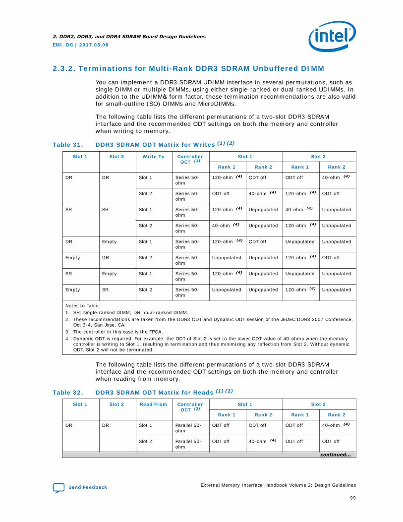
2.3.2. Terminations for Multi-Rank DDR3 SDRAM Unbuffered DIMM
You can implement a DDR3 SDRAM UDIMM interface in several permutations, such assingle DIMM or multiple DIMMs, using either single-ranked or dual-ranked UDIMMs. Inaddition to the UDIMM’s form factor, these termination recommendations are also validfor small-outline (SO) DIMMs and MicroDIMMs.
The following table lists the different permutations of a two-slot DDR3 SDRAMinterface and the recommended ODT settings on both the memory and controllerwhen writing to memory.
Table 31. DDR3 SDRAM ODT Matrix for Writes (1) (2)
Slot 1 Slot 2 Write To ControllerOCT (3)
Slot 1 Slot 2
Rank 1 Rank 2 Rank 1 Rank 2
DR DR Slot 1 Series 50-ohm
120-ohm (4) ODT off ODT off 40-ohm (4)
Slot 2 Series 50-ohm
ODT off 40-ohm (4) 120-ohm (4) ODT off
SR SR Slot 1 Series 50-ohm
120-ohm (4) Unpopulated 40-ohm (4) Unpopulated
Slot 2 Series 50-ohm
40-ohm (4) Unpopulated 120-ohm (4) Unpopulated
DR Empty Slot 1 Series 50-ohm
120-ohm (4) ODT off Unpopulated Unpopulated
Empty DR Slot 2 Series 50-ohm
Unpopulated Unpopulated 120-ohm (4) ODT off
SR Empty Slot 1 Series 50-ohm
120-ohm (4) Unpopulated Unpopulated Unpopulated
Empty SR Slot 2 Series 50-ohm
Unpopulated Unpopulated 120-ohm (4) Unpopulated
Notes to Table:1. SR: single-ranked DIMM; DR: dual-ranked DIMM.2. These recommendations are taken from the DDR3 ODT and Dynamic ODT session of the JEDEC DDR3 2007 Conference,
Oct 3-4, San Jose, CA.3. The controller in this case is the FPGA.4. Dynamic ODT is required. For example, the ODT of Slot 2 is set to the lower ODT value of 40-ohms when the memory
controller is writing to Slot 1, resulting in termination and thus minimizing any reflection from Slot 2. Without dynamicODT, Slot 2 will not be terminated.
The following table lists the different permutations of a two-slot DDR3 SDRAMinterface and the recommended ODT settings on both the memory and controllerwhen reading from memory.
Table 32. DDR3 SDRAM ODT Matrix for Reads (1) (2)
Slot 1 Slot 2 Read From ControllerOCT (3)
Slot 1 Slot 2
Rank 1 Rank 2 Rank 1 Rank 2
DR DR Slot 1 Parallel 50-ohm
ODT off ODT off ODT off 40-ohm (4)
Slot 2 Parallel 50-ohm
ODT off 40-ohm (4) ODT off ODT off
continued...
2. DDR2, DDR3, and DDR4 SDRAM Board Design Guidelines
EMI_DG | 2017.05.08
Send Feedback External Memory Interface Handbook Volume 2: Design Guidelines
99
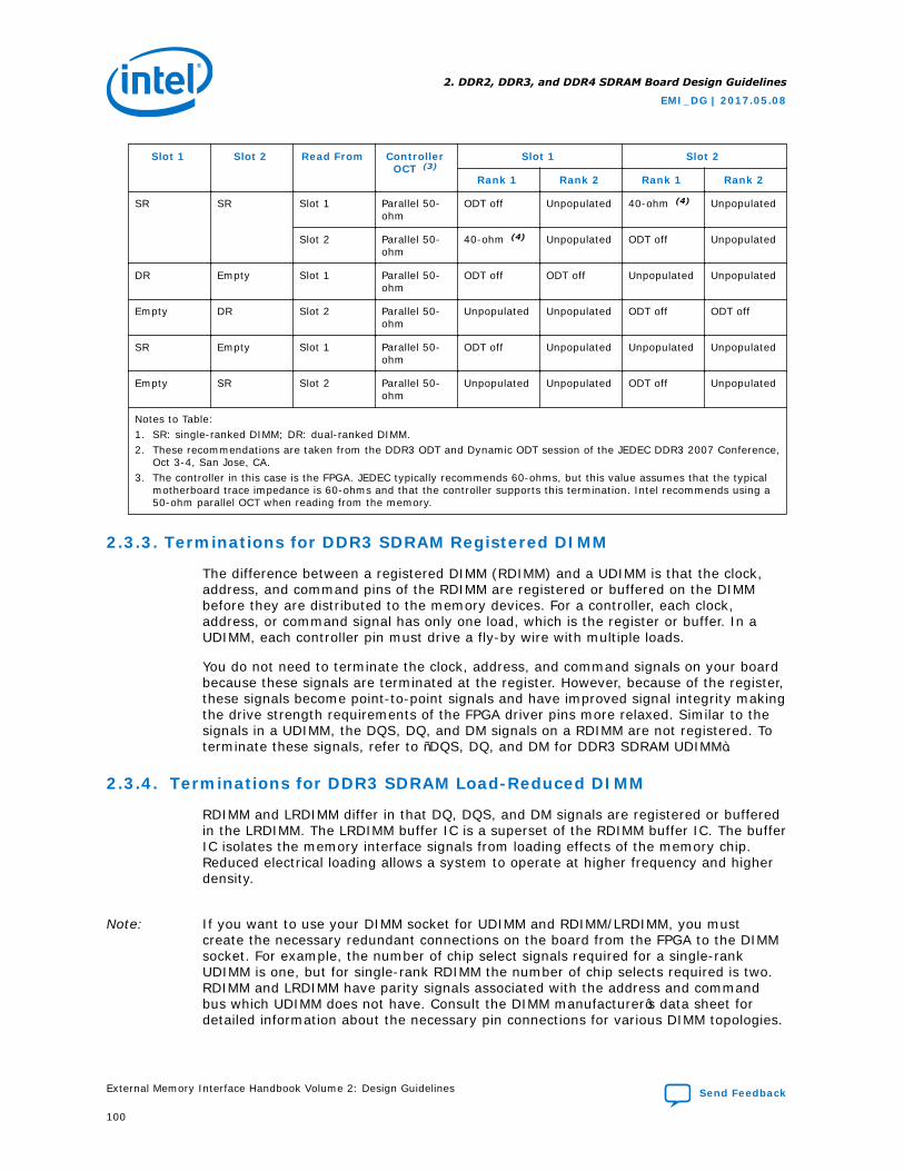
Slot 1 Slot 2 Read From ControllerOCT (3)
Slot 1 Slot 2
Rank 1 Rank 2 Rank 1 Rank 2
SR SR Slot 1 Parallel 50-ohm
ODT off Unpopulated 40-ohm (4) Unpopulated
Slot 2 Parallel 50-ohm
40-ohm (4) Unpopulated ODT off Unpopulated
DR Empty Slot 1 Parallel 50-ohm
ODT off ODT off Unpopulated Unpopulated
Empty DR Slot 2 Parallel 50-ohm
Unpopulated Unpopulated ODT off ODT off
SR Empty Slot 1 Parallel 50-ohm
ODT off Unpopulated Unpopulated Unpopulated
Empty SR Slot 2 Parallel 50-ohm
Unpopulated Unpopulated ODT off Unpopulated
Notes to Table:1. SR: single-ranked DIMM; DR: dual-ranked DIMM.2. These recommendations are taken from the DDR3 ODT and Dynamic ODT session of the JEDEC DDR3 2007 Conference,
Oct 3-4, San Jose, CA.3. The controller in this case is the FPGA. JEDEC typically recommends 60-ohms, but this value assumes that the typical
motherboard trace impedance is 60-ohms and that the controller supports this termination. Intel recommends using a50-ohm parallel OCT when reading from the memory.
2.3.3. Terminations for DDR3 SDRAM Registered DIMM
The difference between a registered DIMM (RDIMM) and a UDIMM is that the clock,address, and command pins of the RDIMM are registered or buffered on the DIMMbefore they are distributed to the memory devices. For a controller, each clock,address, or command signal has only one load, which is the register or buffer. In aUDIMM, each controller pin must drive a fly-by wire with multiple loads.
You do not need to terminate the clock, address, and command signals on your boardbecause these signals are terminated at the register. However, because of the register,these signals become point-to-point signals and have improved signal integrity makingthe drive strength requirements of the FPGA driver pins more relaxed. Similar to thesignals in a UDIMM, the DQS, DQ, and DM signals on a RDIMM are not registered. Toterminate these signals, refer to “DQS, DQ, and DM for DDR3 SDRAM UDIMM”.
2.3.4. Terminations for DDR3 SDRAM Load-Reduced DIMM
RDIMM and LRDIMM differ in that DQ, DQS, and DM signals are registered or bufferedin the LRDIMM. The LRDIMM buffer IC is a superset of the RDIMM buffer IC. The bufferIC isolates the memory interface signals from loading effects of the memory chip.Reduced electrical loading allows a system to operate at higher frequency and higherdensity.
Note: If you want to use your DIMM socket for UDIMM and RDIMM/LRDIMM, you mustcreate the necessary redundant connections on the board from the FPGA to the DIMMsocket. For example, the number of chip select signals required for a single-rankUDIMM is one, but for single-rank RDIMM the number of chip selects required is two.RDIMM and LRDIMM have parity signals associated with the address and commandbus which UDIMM does not have. Consult the DIMM manufacturer’s data sheet fordetailed information about the necessary pin connections for various DIMM topologies.
2. DDR2, DDR3, and DDR4 SDRAM Board Design Guidelines
EMI_DG | 2017.05.08
External Memory Interface Handbook Volume 2: Design Guidelines Send Feedback
100
2.3.5. Terminations for DDR3 SDRAM Components With Leveling
The following topics discusses terminations used to achieve optimum performance fordesigning the DDR3 SDRAM interface using discrete DDR3 SDRAM components.
In addition to using DDR3 SDRAM DIMM to implement your DDR3 SDRAM interface,you can also use DDR3 SDRAM components. However, for applications that havelimited board real estate, using DDR3 SDRAM components reduces the need for aDIMM connector and places components closer, resulting in denser layouts.
2.3.5.1. DDR3 SDRAM Components With or Without Leveling
The DDR3 SDRAM UDIMM is laid out to the JEDEC specification. The JEDECspecification is available from either the JEDEC Organization website (www.JEDEC.org)or from the memory vendors. However, when you are designing the DDR3 SDRAMinterface using discrete SDRAM components, you may desire a layout scheme that isdifferent than the DIMM specification.
You have the following options:
• Mimic the standard DDR3 SDRAM DIMM, using a fly-by topology for the memoryclocks, address, and command signals. This option needs read and write leveling,so you must use the UniPHY IP with leveling.
• Mimic a standard DDR2 SDRAM DIMM, using a balanced (symmetrical) tree-typetopology for the memory clocks, address, and command signals. Using thistopology results in unwanted stubs on the command, address, and clock, whichdegrades signal integrity and limits the performance of the DDR3 SDRAMinterface.
Related Information
• Layout Guidelines for DDR3 and DDR4 SDRAM Interfaces on page 113
• www.JEDEC.org
2.4. DDR3 and DDR4 on Arria 10 and Stratix 10 Devices
The following topics describe considerations specific to DDR3 and DDR4 externalmemory interface protocols on Arria 10 and Stratix 10 devices.
Related Information
www.JEDEC.org
2.4.1. Dynamic On-Chip Termination (OCT) in Arria 10 and Stratix 10Devices
Depending upon the Rs (series) and Rt (parallel) OCT values that you want, youshould choose appropriate values for the RZQ resistor and connect this resistor to theRZQ pin of the FPGA.
• Select a 240-ohm reference resistor to ground to implement Rs OCT values of 34-ohm, 40-ohm, 48-ohm, 60-ohm, and 80-ohm, and Rt OCT resistance values of 20-ohm, 30-ohm, 34-ohm, 40-ohm, 60-ohm, 80-ohm, 120-ohm and 240 ohm.
• Select a 100-ohm reference resistor to ground to implement Rs OCT values of 25-ohm and 50-ohm, and an RT OCT resistance of 50-ohm.
2. DDR2, DDR3, and DDR4 SDRAM Board Design Guidelines
EMI_DG | 2017.05.08
Send Feedback External Memory Interface Handbook Volume 2: Design Guidelines
101
Check the FPGA I/O tab of the parameter editor to determine the I/O standards andtermination values supported for data, address and command, and memory clocksignals.
2.4.2. Dynamic On-Die Termination (ODT) in DDR4
In DDR4, in addition to the Rtt_nom and Rtt_wr values, which are applied during readand write respectively, a third option called Rtt_park is available. When Rtt_park isenabled, a selected termination value is set in the DRAM when ODT is driven low.
Rtt_nom and Rtt_wr work the same as in DDR3, which is described in Dynamic ODTfor DDR3.
Refer to the DDR4 JEDEC specification or your memory vendor data sheet for detailsabout available termination values and functional description for dynamic ODT inDDR4 devices.
For DDR4 LRDIMM, if SPD byte 152 calls for different values of Rtt_Park to be usedfor package ranks 0 and 1 versus package ranks 2 and 3, set the value to the larger ofthe two impedance settings.
2.4.3. Choosing Terminations on Arria 10 Devices
To determine optimal on-chip termination (OCT) and on-die termination (ODT) valuesfor best signal integrity, you should simulate your memory interface in HyperLynx or asimilar tool.
If the optimal OCT and ODT termination values as determined by simulation are notavailable in the list of available values in the parameter editor, select the closestavailable termination values for OCT and ODT.
Refer to Dynamic On-Chip Termination (OCT) in Arria 10 Devices for examples ofvarious OCT modes. Refer to the Arria 10 Device Handbook for more informationabout OCT. For information on available ODT choices, refer to your memory vendordata sheet.
Related Information
Dynamic On-Chip Termination (OCT) in Arria 10 and Stratix 10 Devices on page 87
2.4.4. On-Chip Termination Recommendations for DDR3 and DDR4 onArria 10 Devices
• Output mode (drive strength) for Address/Command/Clock and Data Signals:Depending upon the I/O standard that you have selected, you would have a rangeof selections expressed in terms of ohms or miliamps. A value of 34 to 40 ohms or12 mA is a good starting point for output mode drive strength.
• Input mode (parallel termination) for Data and Data Strobe signals: A value of 40or 60 ohms is a good starting point for FPGA side input termination.
2. DDR2, DDR3, and DDR4 SDRAM Board Design Guidelines
EMI_DG | 2017.05.08
External Memory Interface Handbook Volume 2: Design Guidelines Send Feedback
102
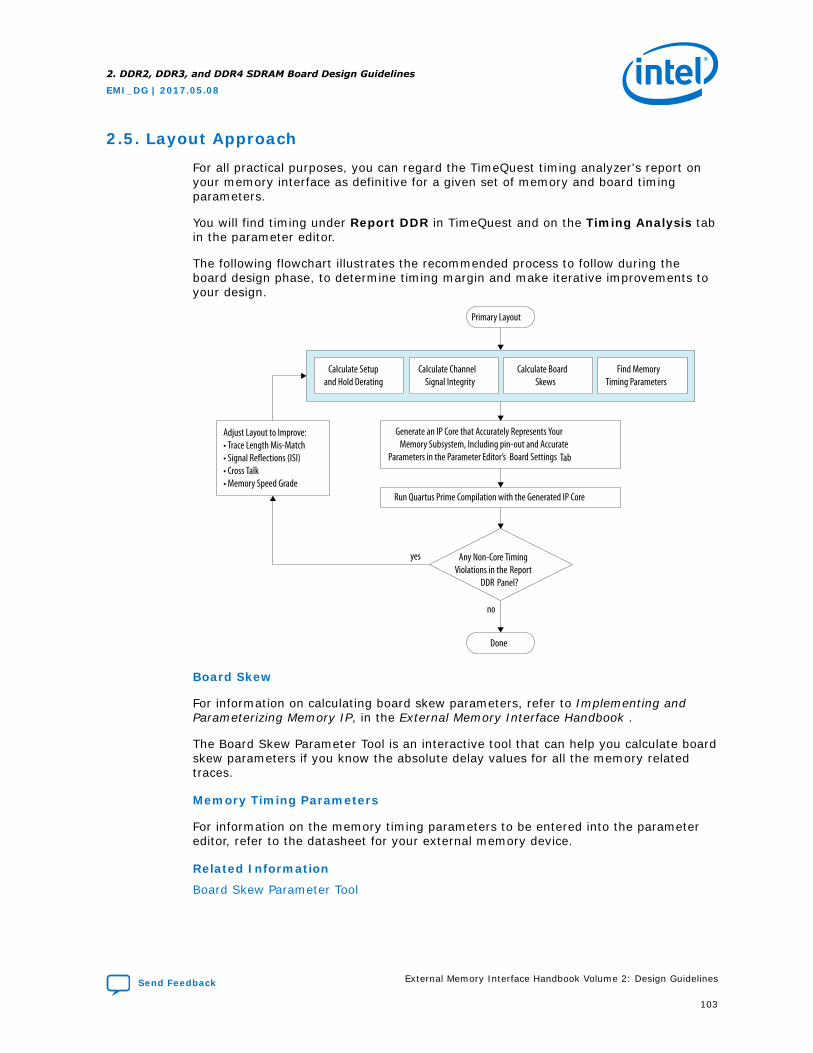
2.5. Layout Approach
For all practical purposes, you can regard the TimeQuest timing analyzer's report onyour memory interface as definitive for a given set of memory and board timingparameters.
You will find timing under Report DDR in TimeQuest and on the Timing Analysis tabin the parameter editor.
The following flowchart illustrates the recommended process to follow during theboard design phase, to determine timing margin and make iterative improvements toyour design.
Primary Layout
Calculate Setupand Hold Derating
Calculate ChannelSignal Integrity
Calculate BoardSkews
Find MemoryTiming Parameters
Generate an IP Core that Accurately Represents Your Memory Subsystem, Including pin-out and Accurate
Parameters in the Parameter Editor’s Board Settings Tab
Run Quartus Prime Compilation with the Generated IP Core
Any Non-Core TimingViolations in the Report
DDR Panel?
yes
no
Done
Adjust Layout to Improve:• Trace Length Mis-Match• Signal Reflections (ISI)• Cross Talk• Memory Speed Grade
Board Skew
For information on calculating board skew parameters, refer to Implementing andParameterizing Memory IP, in the External Memory Interface Handbook .
The Board Skew Parameter Tool is an interactive tool that can help you calculate boardskew parameters if you know the absolute delay values for all the memory relatedtraces.
Memory Timing Parameters
For information on the memory timing parameters to be entered into the parametereditor, refer to the datasheet for your external memory device.
Related Information
Board Skew Parameter Tool
2. DDR2, DDR3, and DDR4 SDRAM Board Design Guidelines
EMI_DG | 2017.05.08
Send Feedback External Memory Interface Handbook Volume 2: Design Guidelines
103
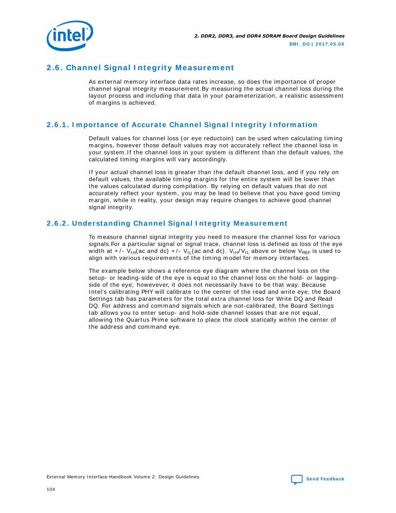
2.6. Channel Signal Integrity Measurement
As external memory interface data rates increase, so does the importance of properchannel signal integrity measurement.By measuring the actual channel loss during thelayout process and including that data in your parameterization, a realistic assessmentof margins is achieved.
2.6.1. Importance of Accurate Channel Signal Integrity Information
Default values for channel loss (or eye reductoin) can be used when calculating timingmargins, however those default values may not accurately reflect the channel loss inyour system.If the channel loss in your system is different than the default values, thecalculated timing margins will vary accordingly.
If your actual channel loss is greater than the default channel loss, and if you rely ondefault values, the available timing margins for the entire system will be lower thanthe values calculated during compilation. By relying on default values that do notaccurately reflect your system, you may be lead to believe that you have good timingmargin, while in reality, your design may require changes to achieve good channelsignal integrity.
2.6.2. Understanding Channel Signal Integrity Measurement
To measure channel signal integrity you need to measure the channel loss for varioussignals.For a particular signal or signal trace, channel loss is defined as loss of the eyewidth at +/- VIH(ac and dc) +/- VIL(ac and dc). VIH/VIL above or below VREF is used toalign with various requirements of the timing model for memory interfaces.
The example below shows a reference eye diagram where the channel loss on thesetup- or leading-side of the eye is equal to the channel loss on the hold- or lagging-side of the eye; howevever, it does not necessarily have to be that way. BecauseIntel's calibrating PHY will calibrate to the center of the read and write eye, the BoardSettings tab has parameters for the total extra channel loss for Write DQ and ReadDQ. For address and command signals which are not-calibrated, the Board Settingstab allows you to enter setup- and hold-side channel losses that are not equal,allowing the Quartus Prime software to place the clock statically within the center ofthe address and command eye.
2. DDR2, DDR3, and DDR4 SDRAM Board Design Guidelines
EMI_DG | 2017.05.08
External Memory Interface Handbook Volume 2: Design Guidelines Send Feedback
104
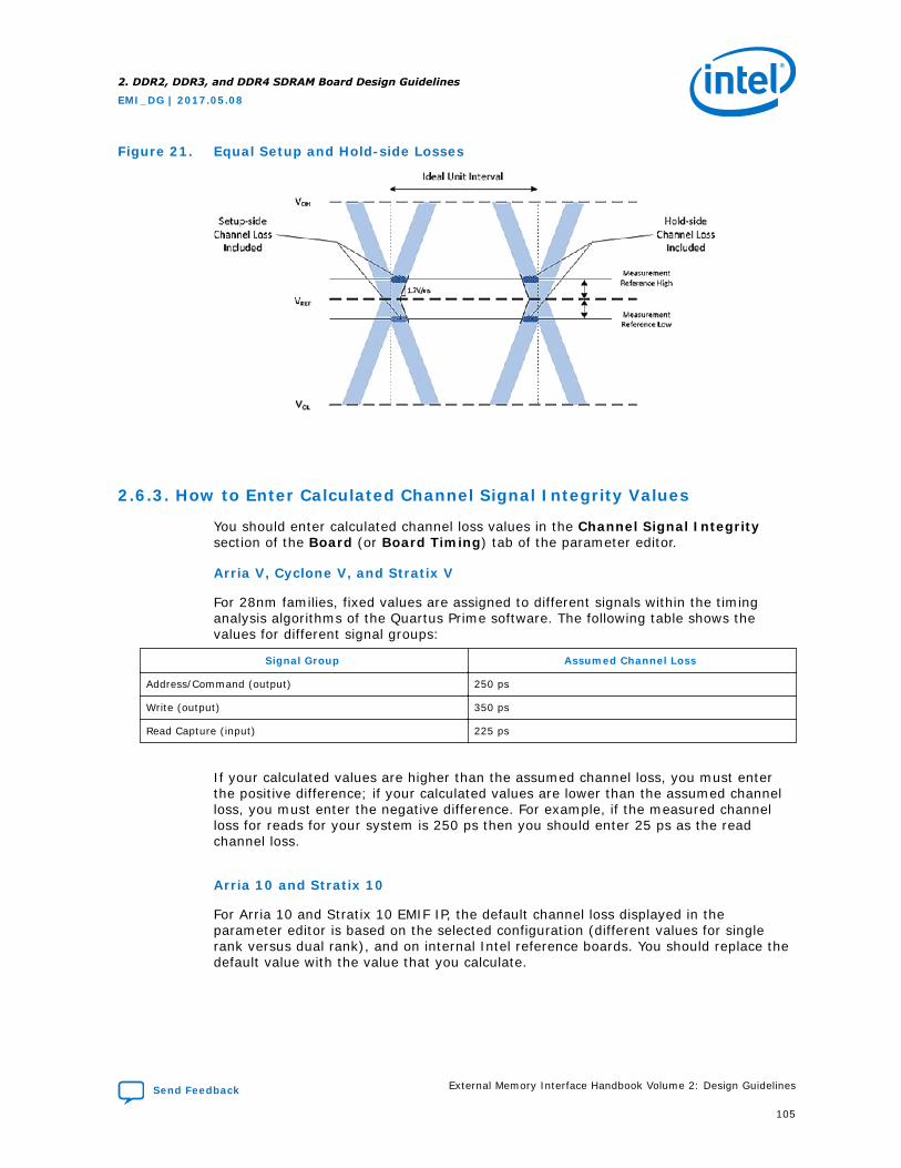
Figure 21. Equal Setup and Hold-side Losses
2.6.3. How to Enter Calculated Channel Signal Integrity Values
You should enter calculated channel loss values in the Channel Signal Integritysection of the Board (or Board Timing) tab of the parameter editor.
Arria V, Cyclone V, and Stratix V
For 28nm families, fixed values are assigned to different signals within the timinganalysis algorithms of the Quartus Prime software. The following table shows thevalues for different signal groups:
Signal Group Assumed Channel Loss
Address/Command (output) 250 ps
Write (output) 350 ps
Read Capture (input) 225 ps
If your calculated values are higher than the assumed channel loss, you must enterthe positive difference; if your calculated values are lower than the assumed channelloss, you must enter the negative difference. For example, if the measured channelloss for reads for your system is 250 ps then you should enter 25 ps as the readchannel loss.
Arria 10 and Stratix 10
For Arria 10 and Stratix 10 EMIF IP, the default channel loss displayed in theparameter editor is based on the selected configuration (different values for singlerank versus dual rank), and on internal Intel reference boards. You should replace thedefault value with the value that you calculate.
2. DDR2, DDR3, and DDR4 SDRAM Board Design Guidelines
EMI_DG | 2017.05.08
Send Feedback External Memory Interface Handbook Volume 2: Design Guidelines
105
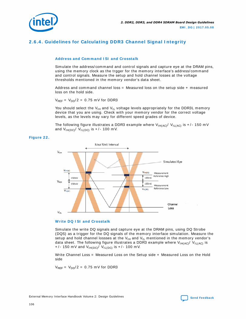
2.6.4. Guidelines for Calculating DDR3 Channel Signal Integrity
Address and Command ISI and Crosstalk
Simulate the address/command and control signals and capture eye at the DRAM pins,using the memory clock as the trgger for the memory interface's address/commandand control signals. Measure the setup and hold channel losses at the voltagethresholds mentioned in the memory vendor's data sheet.
Address and command channel loss = Measured loss on the setup side + measuredloss on the hold side.
VREF = VDD/2 = 0.75 mV for DDR3
You should select the VIH and VIL voltage levels appropriately for the DDR3L memorydevice that you are using. Check with your memory vendor for the correct voltagelevels, as the levels may vary for different speed grades of device.
The following figure illustrates a DDR3 example where VIH(AC)/ VIL(AC) is +/- 150 mVand VIH(DC)/ VIL(DC) is +/- 100 mV.
Figure 22.
Write DQ ISI and Crosstalk
Simulate the write DQ signals and capture eye at the DRAM pins, using DQ Strobe(DQS) as a trigger for the DQ signals of the memory interface simulation. Measure thesetup and hold channel lossses at the VIH and VIL mentioned in the memory vendor'sdata sheet. The following figure illustrates a DDR3 example where VIH(AC)/ VIL(AC) is+/- 150 mV and VIH(DC)/ VIL(DC) is +/- 100 mV.
Write Channel Loss = Measured Loss on the Setup side + Measured Loss on the Holdside
VREF = VDD/2 = 0.75 mV for DDR3
2. DDR2, DDR3, and DDR4 SDRAM Board Design Guidelines
EMI_DG | 2017.05.08
External Memory Interface Handbook Volume 2: Design Guidelines Send Feedback
106
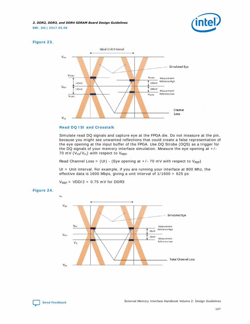
Figure 23.
Read DQ ISI and Crosstalk
Simulate read DQ signals and capture eye at the FPGA die. Do not measure at the pin,because you might see unwanted reflections that could create a false representation ofthe eye opening at the input buffer of the FPGA. Use DQ Strobe (DQS) as a trigger forthe DQ signals of your memory interface simulation. Measure the eye opening at +/-70 mV (VIH/VIL) with respect to VREF.
Read Channel Loss = (UI) - (Eye opening at +/- 70 mV with respect to VREF)
UI = Unit interval. For example, if you are running your interface at 800 Mhz, theeffective data is 1600 Mbps, giving a unit interval of 1/1600 = 625 ps
VREF = VDD/2 = 0.75 mV for DDR3
Figure 24.
2. DDR2, DDR3, and DDR4 SDRAM Board Design Guidelines
EMI_DG | 2017.05.08
Send Feedback External Memory Interface Handbook Volume 2: Design Guidelines
107
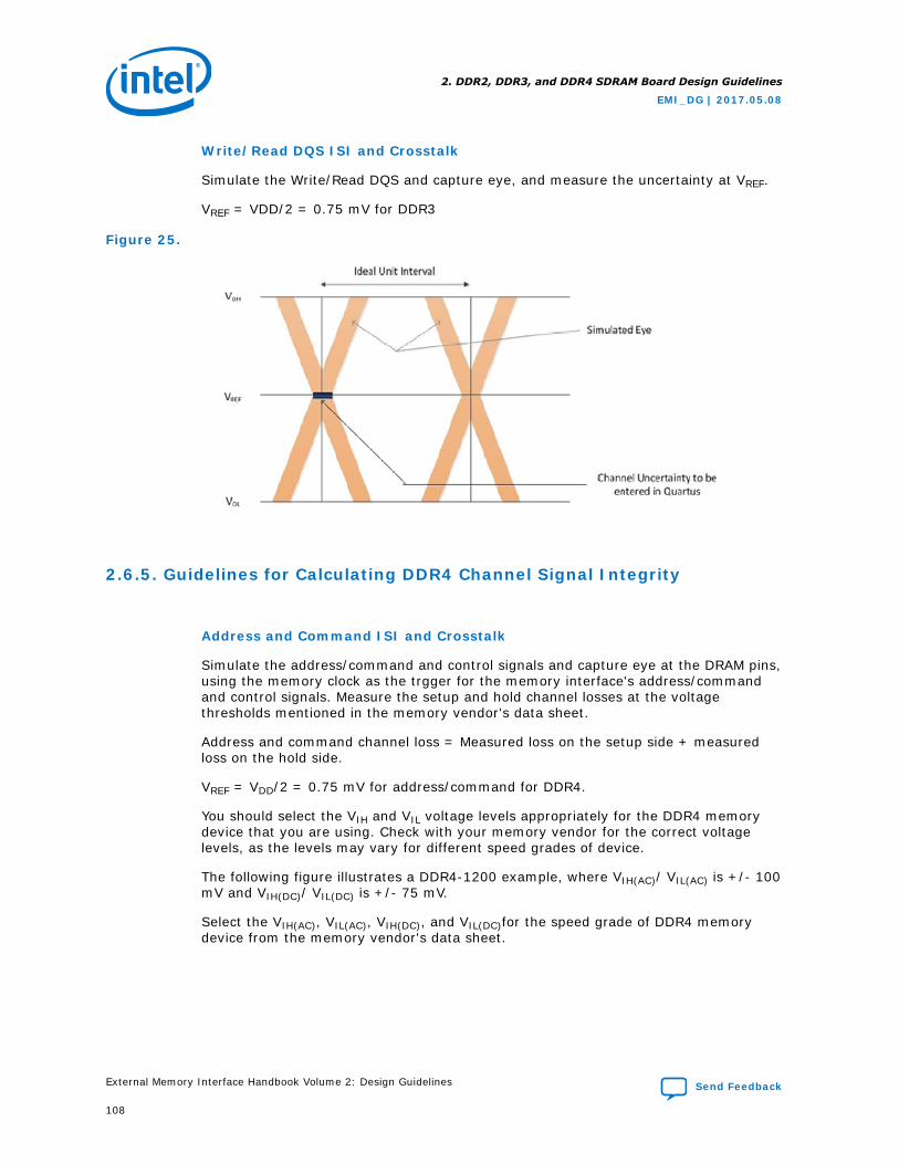
Write/Read DQS ISI and Crosstalk
Simulate the Write/Read DQS and capture eye, and measure the uncertainty at VREF.
VREF = VDD/2 = 0.75 mV for DDR3
Figure 25.
2.6.5. Guidelines for Calculating DDR4 Channel Signal Integrity
Address and Command ISI and Crosstalk
Simulate the address/command and control signals and capture eye at the DRAM pins,using the memory clock as the trgger for the memory interface's address/commandand control signals. Measure the setup and hold channel losses at the voltagethresholds mentioned in the memory vendor's data sheet.
Address and command channel loss = Measured loss on the setup side + measuredloss on the hold side.
VREF = VDD/2 = 0.75 mV for address/command for DDR4.
You should select the VIH and VIL voltage levels appropriately for the DDR4 memorydevice that you are using. Check with your memory vendor for the correct voltagelevels, as the levels may vary for different speed grades of device.
The following figure illustrates a DDR4-1200 example, where VIH(AC)/ VIL(AC) is +/- 100mV and VIH(DC)/ VIL(DC) is +/- 75 mV.
Select the VIH(AC), VIL(AC), VIH(DC), and VIL(DC)for the speed grade of DDR4 memorydevice from the memory vendor's data sheet.
2. DDR2, DDR3, and DDR4 SDRAM Board Design Guidelines
EMI_DG | 2017.05.08
External Memory Interface Handbook Volume 2: Design Guidelines Send Feedback
108
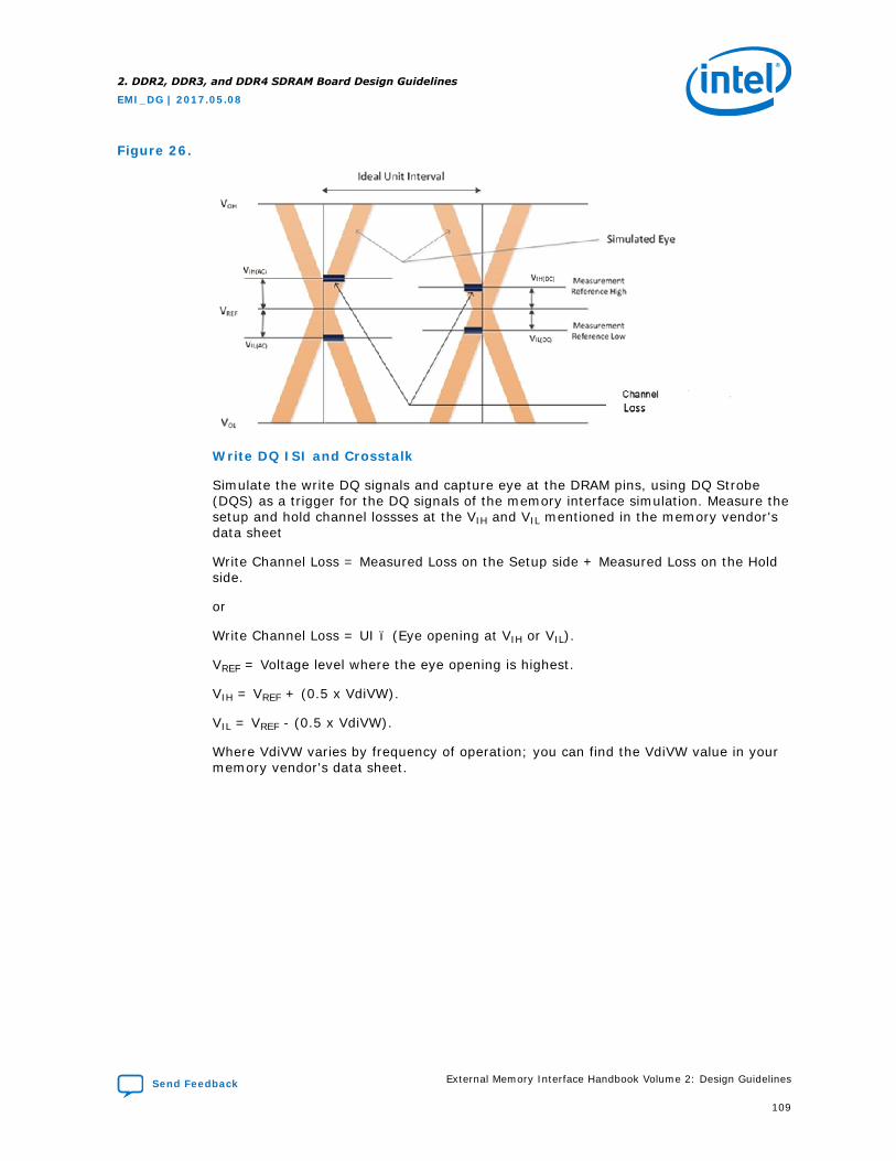
Figure 26.
Write DQ ISI and Crosstalk
Simulate the write DQ signals and capture eye at the DRAM pins, using DQ Strobe(DQS) as a trigger for the DQ signals of the memory interface simulation. Measure thesetup and hold channel lossses at the VIH and VIL mentioned in the memory vendor'sdata sheet
Write Channel Loss = Measured Loss on the Setup side + Measured Loss on the Holdside.
or
Write Channel Loss = UI – (Eye opening at VIH or VIL).
VREF = Voltage level where the eye opening is highest.
VIH = VREF + (0.5 x VdiVW).
VIL = VREF - (0.5 x VdiVW).
Where VdiVW varies by frequency of operation; you can find the VdiVW value in yourmemory vendor's data sheet.
2. DDR2, DDR3, and DDR4 SDRAM Board Design Guidelines
EMI_DG | 2017.05.08
Send Feedback External Memory Interface Handbook Volume 2: Design Guidelines
109
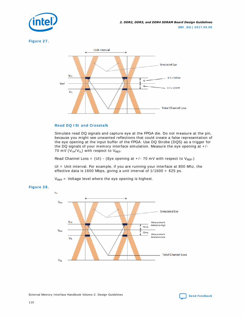
Figure 27.
Read DQ ISI and Crosstalk
Simulate read DQ signals and capture eye at the FPGA die. Do not measure at the pin,because you might see unwanted reflections that could create a false representation ofthe eye opening at the input buffer of the FPGA. Use DQ Strobe (DQS) as a trigger forthe DQ signals of your memory interface simulation. Measure the eye opening at +/-70 mV (VIH/VIL) with respect to VREF.
Read Channel Loss = (UI) - (Eye opening at +/- 70 mV with respect to VREF.)
UI = Unit interval. For example, if you are running your interface at 800 Mhz, theeffective data is 1600 Mbps, giving a unit interval of 1/1600 = 625 ps.
VREF = Voltage level where the eye opening is highest.
Figure 28.
2. DDR2, DDR3, and DDR4 SDRAM Board Design Guidelines
EMI_DG | 2017.05.08
External Memory Interface Handbook Volume 2: Design Guidelines Send Feedback
110
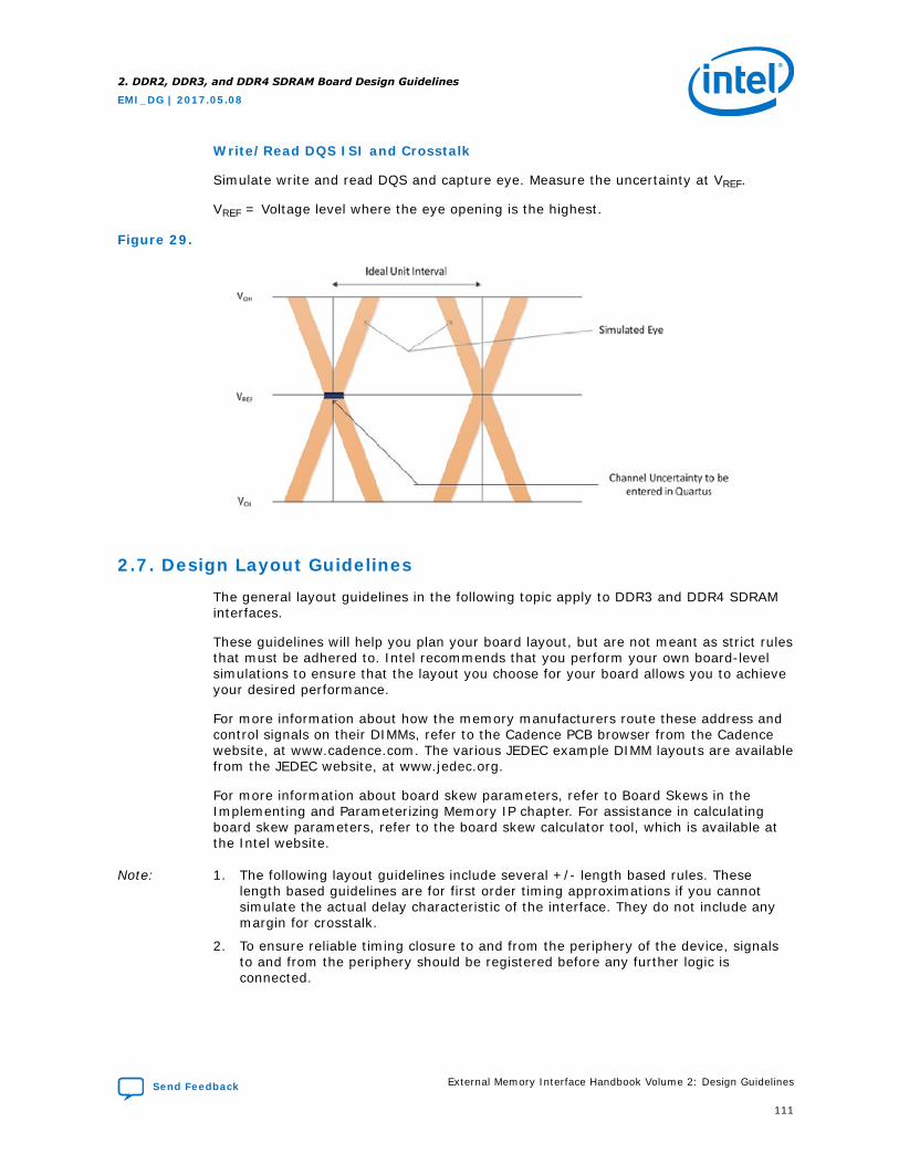
Write/Read DQS ISI and Crosstalk
Simulate write and read DQS and capture eye. Measure the uncertainty at VREF.
VREF = Voltage level where the eye opening is the highest.
Figure 29.
2.7. Design Layout Guidelines
The general layout guidelines in the following topic apply to DDR3 and DDR4 SDRAMinterfaces.
These guidelines will help you plan your board layout, but are not meant as strict rulesthat must be adhered to. Intel recommends that you perform your own board-levelsimulations to ensure that the layout you choose for your board allows you to achieveyour desired performance.
For more information about how the memory manufacturers route these address andcontrol signals on their DIMMs, refer to the Cadence PCB browser from the Cadencewebsite, at www.cadence.com. The various JEDEC example DIMM layouts are availablefrom the JEDEC website, at www.jedec.org.
For more information about board skew parameters, refer to Board Skews in theImplementing and Parameterizing Memory IP chapter. For assistance in calculatingboard skew parameters, refer to the board skew calculator tool, which is available atthe Intel website.
Note: 1. The following layout guidelines include several +/- length based rules. Theselength based guidelines are for first order timing approximations if you cannotsimulate the actual delay characteristic of the interface. They do not include anymargin for crosstalk.
2. To ensure reliable timing closure to and from the periphery of the device, signalsto and from the periphery should be registered before any further logic isconnected.
2. DDR2, DDR3, and DDR4 SDRAM Board Design Guidelines
EMI_DG | 2017.05.08
Send Feedback External Memory Interface Handbook Volume 2: Design Guidelines
111
Intel recommends that you get accurate time base skew numbers for your designwhen you simulate the specific implementation.
Related Information
• www.JEDEC.org
• www.cadence.com
• www.mentor.com
• Board Skew Parameters Tool
• http://www.jedec.org/download/DesignFiles/DDR2/default1.cfm
2.7.1. General Layout Guidelines
The following table lists general board design layout guidelines. These guidelines areIntel recommendations, and should not be considered as hard requirements. Youshould perform signal integrity simulation on all the traces to verify the signal integrityof the interface. You should extract the slew rate and propagation delay information,enter it into the IP and compile the design to ensure that timing requirements aremet.
Table 33. General Layout Guidelines
Parameter Guidelines
Impedance • All unused via pads must be removed, because they cause unwantedcapacitance.
• Trace impedance plays an important role in the signal integrity. You mustperform board level simulation to determine the best characteristic impedancefor your PCB. For example, it is possible that for multi rank systems 40 ohmscould yield better results than a traditional 50 ohm characteristic impedance.
Decoupling Parameter • Use 0.1 uF in 0402 size to minimize inductance• Make VTT voltage decoupling close to termination resistors• Connect decoupling caps between VTT and ground• Use a 0.1 uF cap for every other VTT pin and 0.01 uF cap for every VDD and
VDDQ pin• Verify the capacitive decoupling using the Intel Power Distribution Network
Design Tool
Power • Route GND and VCC as planes• Route VCCIO for memories in a single split plane with at least a 20-mil
(0.020 inches, or 0.508 mm) gap of separation• Route VTT as islands or 250-mil (6.35-mm) power traces• Route oscillators and PLL power as islands or 100-mil (2.54-mm) power traces
General Routing All specified delay matching requirements include PCB trace delays, different layerpropagation velocity variance, and crosstalk. To minimize PCB layer propogationvariance, Intel recommends that signals from the same net group always berouted on the same layer.• Use 45° angles (not 90° corners)• Avoid T-Junctions for critical nets or clocks• Avoid T-junctions greater than 250 mils (6.35 mm)• Disallow signals across split planes• Restrict routing other signals close to system reset signals• Avoid routing memory signals closer than 0.025 inch (0.635 mm) to PCI or
system clocks
Related Information
Power Distribution Network Design Tool
2. DDR2, DDR3, and DDR4 SDRAM Board Design Guidelines
EMI_DG | 2017.05.08
External Memory Interface Handbook Volume 2: Design Guidelines Send Feedback
112
2.7.2. Layout Guidelines for DDR3 and DDR4 SDRAM Interfaces
The following table lists DDR3 and DDR4 SDRAM layout guidelines.
Unless otherwise specified, the guidelines in the following table apply to the followingtopologies:
• DIMM—UDIMM topology
• DIMM—RDIMM topology
• DIMM—LRDIMM topology
• Not all versions of the Quartus Prime software support LRDIMM.
• Discrete components laid out in UDIMM topology
• Discrete components laid out in RDIMM topology
These guidelines are recommendations, and should not be considered as hardrequirements. You should perform signal integrity simulation on all the traces to verifythe signal integrity of the interface.
Unless stated otherwise, the following guidelines apply to all devices that supportDDR3 or DDR4, including Arria 10 and Stratix 10.
For information on the simulation flow for 28nm products, refer to http://www.alterawiki.com/wiki/Measuring_Channel_Signal_Integrity.
For information on the simulation flow for Arria 10 products, refer to http://www.alterawiki.com/wiki/Arria_10_EMIF_Simulation_Guidance.
http://www.altera.com/technology/memory/estimator/mem-emif-index.html
For supported frequencies and topologies, refer to the External Memory Interface SpecEstimator http://www.altera.com/technology/memory/estimator/mem-emif-index.html.
For frequencies greater than 800 MHz, when you are calculating the delay associatedwith a trace, you must take the FPGA package delays into consideration. For moreinformation, refer to Package Deskew.
For device families that do not support write leveling, refer to Layout Guidelines forDDR2 SDRAM Interfaces.
Table 34. DDR3 and DDR4 SDRAM Layout Guidelines (1)
Parameter Guidelines
Decoupling Parameter • Make VTT voltage decoupling close to the components and pull-up resistors.• Connect decoupling caps between VTT and VDD using a 0.1F cap for every
other VTT pin.• Use a 0.1 uF cap and 0.01 uF cap for every VDDQ pin.
Maximum Trace Length (2) • Even though there are no hard requirements for minimum trace length, youneed to simulate the trace to ensure the signal integrity. Shorter routes resultin better timing.
• For DIMM topology only:• Maximum trace length for all signals from FPGA to the first DIMM slot is 4.5
inches.• Maximum trace length for all signals from DIMM slot to DIMM slot is 0.425
inches.
continued...
2. DDR2, DDR3, and DDR4 SDRAM Board Design Guidelines
EMI_DG | 2017.05.08
Send Feedback External Memory Interface Handbook Volume 2: Design Guidelines
113

Parameter Guidelines
• For discrete components only:• Maximum trace length for address, command, control, and clock from FPGA to
the first component must not be more than 7 inches.• Maximum trace length for DQ, DQS, DQS#, and DM from FPGA to the first
component is 5 inches.
General Routing • Route over appropriate VCC and GND planes.• Keep signal routing layers close to GND and power planes.
Spacing Guidelines • Avoid routing two signal layers next to each other. Always make sure that thesignals related to memory interface are routed between appropriate GND orpower layers.
• For DQ/DQS/DM traces: Maintain at least 3H spacing between the edges (air-gap) for these traces. (Where H is the vertical distance to the closest returnpath for that particular trace.)
• For Address/Command/Control traces: Maintain at least 3H spacing betweenthe edges (air-gap) these traces. (Where H is the vertical distance to theclosest return path for that particular trace.)
• For Clock traces: Maintain at least 5H spacing between two clock pair or aclock pair and any other memory interface trace. (Where H is the verticaldistance to the closest return path for that particular trace.)
Clock Routing • Route clocks on inner layers with outer-layer run lengths held to under 500mils (12.7 mm).
• Route clock signals in a daisy chain topology from the first SDRAM to the lastSDRAM. The maximum length of the first SDRAM to the last SDRAM must notexceed 0.69 tCK for DDR3 and 1.5 tCK for DDR4. For different DIMMconfigurations, check the appropriate JEDEC specification.
• These signals should maintain the following spacings:• Clocks should maintain a length-matching between clock pairs of ±5 ps.• Clocks should maintain a length-matching between positive (p) and negative
(n) signals of ±2 ps, routed in parallel.• Space between different pairs should be at least two times the trace width of
the differential pair to minimize loss and maximize interconnect density.• To avoid mismatched transmission line to via, Intel recommends that you use
Ground Signal Signal Ground (GSSG) topology for your clock pattern—GND|CLKP|CKLN|GND.
• Route all addresses and commands to match the clock signals to within ±20 psto each discrete memory component. Refer to the following figure.
Address and Command Routing • Route address and command signals in a daisy chain topology from the firstSDRAM to the last SDRAM. The maximum length of the first SDRAM to the lastSDRAM must not be more than 0.69 tCK for DDR3 and 1.5 tCK for DDR4. Fordifferent DIMM configurations, check the appropriate JEDEC specifications.
• UDIMMs are more susceptible to cross-talk and are generally noisier thanbuffered DIMMs. Therefore, route address and command signals of UDIMMs ona different layer than data signals (DQ) and data mask signals (DM) and withgreater spacing.
• Do not route differential clock (CK) and clock enable (CKE) signals close toaddress signals.
• Route all addresses and commands to match the clock signals to within ±20 psto each discrete memory component. Refer to the following figure.
continued...
2. DDR2, DDR3, and DDR4 SDRAM Board Design Guidelines
EMI_DG | 2017.05.08
External Memory Interface Handbook Volume 2: Design Guidelines Send Feedback
114
Parameter Guidelines
DQ, DM, and DQS Routing Rules • All the trace length matching requirements are from the FPGA package ball tothe SDRAM package ball, which means you must consider trace mismatchingon different DIMM raw cards.
• Match in length all DQ, DQS, and DM signals within a given byte-lane groupwith a maximum deviation of ±10 ps.
• Ensure to route all DQ, DQS, and DM signals within a given byte-lane group onthe same layer to avoid layer to layer transmission velocity differences, whichotherwise increase the skew within the group.
• Do not count on FPGAs to deskew for more than 20 ps of DQ group skew. Theskew algorithm only removes the following possible uncertainties:— Minimum and maximum die IOE skew or delay mismatch— Minimum and maximum device package skew or mismatch— Board delay mismatch of 20 ps— Memory component DQ skew mismatch— Increasing any of these four parameters runs the risk of the deskew
algorithm limiting, failing to correct for the total observed system skew. Ifthe algorithm cannot compensate without limiting the correction, timinganalysis shows reduced margins.
• For memory interfaces with leveling, the timing between the DQS and clocksignals on each device calibrates dynamically to meet tDQSS. To make surethe skew is not too large for the leveling circuit’s capability, follow these rules:— Propagation delay of clock signal must not be shorter than propagation
delay of DQS signal at every device: (CKi) – DQSi > 0; 0 < i < number ofcomponents – 1 . For DIMMs, ensure that the CK trace is longer than thelongest DQS trace at the DIMM connector.
— Total skew of CLK and DQS signal between groups is less than one clockcycle: (CKi+ DQSi) max – (CKi+ DQSi) min < 1 × tCK(If you are using aDIMM topology, your delay and skew must take into consideration valuesfor the actual DIMM.)
Spacing Guidelines • Avoid routing two signal layers next to each other. Always ensure that thesignals related to the memory interface are routed between appropriate GNDor power layers.
• For DQ/DQS/DM traces: Maintain at least 3H spacing between the edges (air-gap) of these traces, where H is the vertical distance to the closest return pathfor that particular trace.
• For Address/Command/Control traces: Maintain at least 3H spacing betweenthe edges (air-gap) of these traces, where H is the vertical distance to theclosest return path for that particular trace.
• For Clock traces: Maintain at least 5H spacing between two clock pairs or aclock pair and any other memory interface trace, where H is the verticaldistance to the closest return path for that particular trace.
Quartus Prime Software Settings forBoard Layout
• To perform timing analyses on board and I/O buffers, use third partysimulation tool to simulate all timing information such as skew, ISI, crosstalk,and type the simulation result into the UniPHY board setting panel.
• Do not use advanced I/O timing model (AIOT) or board trace model unless youdo not have access to any third party tool. AIOT provides reasonable accuracybut tools like HyperLynx provide better results.
Notes to Table:1. For point-to-point and DIMM interface designs, refer to the Micron website, www.micron.com.2. For better efficiency, the UniPHY IP requires faster turnarounds from read commands to write.
Related Information
• Layout Guidelines for DDR2 SDRAM Interface on page 94
• Package Deskew on page 121
• External Memory Interface Spec Estimator
• www.micron.com
2. DDR2, DDR3, and DDR4 SDRAM Board Design Guidelines
EMI_DG | 2017.05.08
Send Feedback External Memory Interface Handbook Volume 2: Design Guidelines
115
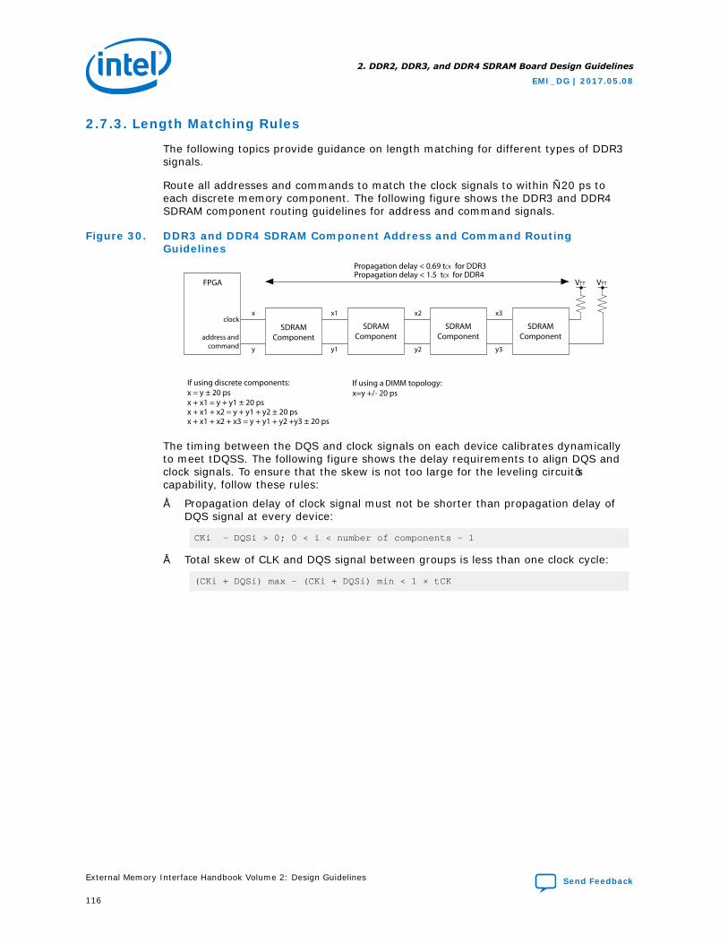
2.7.3. Length Matching Rules
The following topics provide guidance on length matching for different types of DDR3signals.
Route all addresses and commands to match the clock signals to within ±20 ps toeach discrete memory component. The following figure shows the DDR3 and DDR4SDRAM component routing guidelines for address and command signals.
Figure 30. DDR3 and DDR4 SDRAM Component Address and Command RoutingGuidelines
If using discrete components:x = y ± 20 psx + x1 = y + y1 ± 20 psx + x1 + x2 = y + y1 + y2 ± 20 ps
address andcommand
clockx
y
x1
y1
x2
y2
x3
y3
If using a DIMM topology: x=y +/- 20 ps
Propagation delay < 0.69 for DDR3
VTTVTT
SDRAMComponent
SDRAMComponent
SDRAMComponent
SDRAMComponent
FPGA
x + x1 + x2 + x3 = y + y1 + y2 +y3 ± 20 ps
tCK
Propagation delay < 1.5 for DDR4 tCK
The timing between the DQS and clock signals on each device calibrates dynamicallyto meet tDQSS. The following figure shows the delay requirements to align DQS andclock signals. To ensure that the skew is not too large for the leveling circuit’scapability, follow these rules:
• Propagation delay of clock signal must not be shorter than propagation delay ofDQS signal at every device:
CKi – DQSi > 0; 0 < i < number of components – 1
• Total skew of CLK and DQS signal between groups is less than one clock cycle:
(CKi + DQSi) max – (CKi + DQSi) min < 1 × tCK
2. DDR2, DDR3, and DDR4 SDRAM Board Design Guidelines
EMI_DG | 2017.05.08
External Memory Interface Handbook Volume 2: Design Guidelines Send Feedback
116
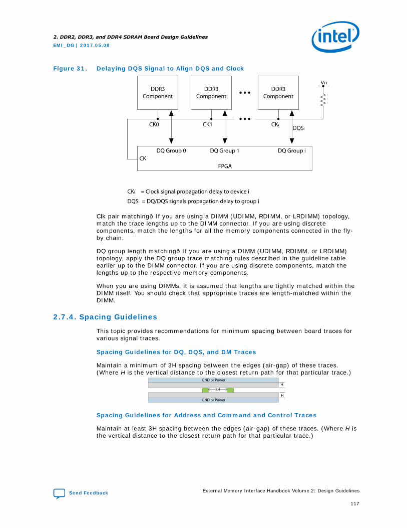
Figure 31. Delaying DQS Signal to Align DQS and Clock
VTT
DDR3Component
DDR3Component
DDR3Component
DQ Group 0CK
CK0 CK1 DQSiCKi
CKi = Clock signal propagation delay to device i
DQSi = DQ/DQS signals propagation delay to group i
FPGA
DQ Group 1 DQ Group i
Clk pair matching—If you are using a DIMM (UDIMM, RDIMM, or LRDIMM) topology,match the trace lengths up to the DIMM connector. If you are using discretecomponents, match the lengths for all the memory components connected in the fly-by chain.
DQ group length matching—If you are using a DIMM (UDIMM, RDIMM, or LRDIMM)topology, apply the DQ group trace matching rules described in the guideline tableearlier up to the DIMM connector. If you are using discrete components, match thelengths up to the respective memory components.
When you are using DIMMs, it is assumed that lengths are tightly matched within theDIMM itself. You should check that appropriate traces are length-matched within theDIMM.
2.7.4. Spacing Guidelines
This topic provides recommendations for minimum spacing between board traces forvarious signal traces.
Spacing Guidelines for DQ, DQS, and DM Traces
Maintain a minimum of 3H spacing between the edges (air-gap) of these traces.(Where H is the vertical distance to the closest return path for that particular trace.)
GND or Power
3HH
GND or PowerH
Spacing Guidelines for Address and Command and Control Traces
Maintain at least 3H spacing between the edges (air-gap) of these traces. (Where H isthe vertical distance to the closest return path for that particular trace.)
2. DDR2, DDR3, and DDR4 SDRAM Board Design Guidelines
EMI_DG | 2017.05.08
Send Feedback External Memory Interface Handbook Volume 2: Design Guidelines
117
GND or Power
3HH
GND or PowerH
Spacing Guidelines for Clock Traces
Maintain at least 5H spacing between two clock pair or a clock pair and any othermemory interface trace. (Where H is the vertical distance to the closest return path forthat particular trace.)
5H
GND or PowerH
HGND or Power
2.7.5. Layout Guidelines for DDR3 and DDR4 SDRAM Wide Interface(>72 bits)
The following topics discuss different ways to lay out a wider DDR3 or DDR4 SDRAMinterface to the FPGA. Choose the topology based on board trace simulation and thetiming budget of your system.
The UniPHY IP supports up to a 144-bit wide DDR3 interface. You can either usediscrete components or DIMMs to implement a wide interface (any interface widerthan 72 bits). Intel recommends using leveling when you implement a wide interfacewith DDR3 components.
When you lay out for a wider interface, all rules and constraints discussed in theprevious sections still apply. The DQS, DQ, and DM signals are point-to-point, and allthe same rules discussed in Design Layout Guidelines apply.
The main challenge for the design of the fly-by network topology for the clock,command, and address signals is to avoid signal integrity issues, and to make sureyou route the DQS, DQ, and DM signals with the chosen topology.
Related Information
Design Layout Guidelines on page 111
2.7.5.1. Fly-By Network Design for Clock, Command, and Address Signals
The UniPHY IP requires the flight-time skew between the first DDR3 SDRAMcomponent and the last DDR3 SDRAM component to be less than 0.69 tCK formemory clocks. This constraint limits the number of components you can have foreach fly-by network.
If you design with discrete components, you can choose to use one or more fly-bynetworks for the clock, command, and address signals.
The following figure shows an example of a single fly-by network topology.
2. DDR2, DDR3, and DDR4 SDRAM Board Design Guidelines
EMI_DG | 2017.05.08
External Memory Interface Handbook Volume 2: Design Guidelines Send Feedback
118
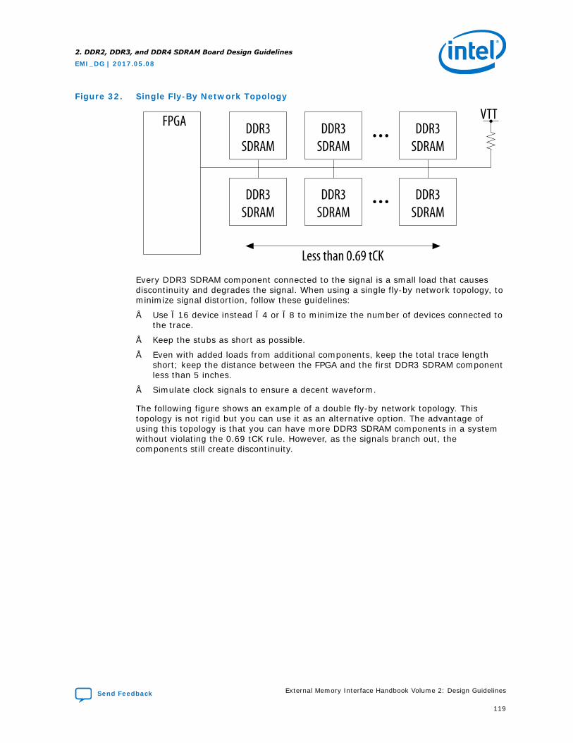
Figure 32. Single Fly-By Network Topology
VTTFPGA DDR3SDRAM
DDR3SDRAM
DDR3SDRAM
DDR3SDRAM
DDR3SDRAM
DDR3SDRAM
Less than 0.69 tCK
Every DDR3 SDRAM component connected to the signal is a small load that causesdiscontinuity and degrades the signal. When using a single fly-by network topology, tominimize signal distortion, follow these guidelines:
• Use ×16 device instead ×4 or ×8 to minimize the number of devices connected tothe trace.
• Keep the stubs as short as possible.
• Even with added loads from additional components, keep the total trace lengthshort; keep the distance between the FPGA and the first DDR3 SDRAM componentless than 5 inches.
• Simulate clock signals to ensure a decent waveform.
The following figure shows an example of a double fly-by network topology. Thistopology is not rigid but you can use it as an alternative option. The advantage ofusing this topology is that you can have more DDR3 SDRAM components in a systemwithout violating the 0.69 tCK rule. However, as the signals branch out, thecomponents still create discontinuity.
2. DDR2, DDR3, and DDR4 SDRAM Board Design Guidelines
EMI_DG | 2017.05.08
Send Feedback External Memory Interface Handbook Volume 2: Design Guidelines
119
Figure 33. Double Fly-By Network Topology
DDR3SDRAM
DDR3SDRAM
DDR3SDRAM
DDR3SDRAM
DDR3SDRAM
DDR3SDRAM
Less than 0.69 t
FPGA
DDR3SDRAM
DDR3SDRAM
DDR3SDRAM
DDR3SDRAM
DDR3SDRAM
DDR3SDRAM
Less than 0.69 t
V TT
V TT
CK
CK
You must perform simulations to find the location of the split, and the best impedancefor the traces before and after the split.
The following figure shows a way to minimize the discontinuity effect. In this example,keep TL2 and TL3 matches in length. Keep TL1 longer than TL2 and TL3, so that it iseasier to route all the signals during layout.
2. DDR2, DDR3, and DDR4 SDRAM Board Design Guidelines
EMI_DG | 2017.05.08
External Memory Interface Handbook Volume 2: Design Guidelines Send Feedback
120
Figure 34. Minimizing Discontinuity Effect
Splitting Point
TL3, ZQ = 50Ω
TL1, ZQ = 25Ω
TL2, ZQ = 50Ω
You can also consider using a DIMM on each branch to replace the components.Because the trade impedance on the DIMM card is 40-ohm to 60-ohm, perform aboard trace simulation to control the reflection to within the level your system cantolerate.
By using the new features of the DDR3 SDRAM controller with UniPHY and theStratix III, Stratix IV, or Stratix V devices, you simplify your design process. Using thefly-by daisy chain topology increases the complexity of the datapath and controllerdesign to achieve leveling, but also greatly improves performance and eases boardlayout for DDR3 SDRAM.
You can also use the DDR3 SDRAM components without leveling in a design if it mayresult in a more optimal solution, or use with devices that support the requiredelectrical interface standard, but do not support the required read and write levelingfunctionality.
2.8. Package Deskew
Trace lengths inside the device package are not uniform for all package pins. Thenonuniformity of package traces can affect system timing for high frequencies. In theQuartus II software version 12.0 and later, and the Quartus Prime software, a packagedeskew option is available.
If you do not enable the package deskew option, the Quartus Prime software uses thepackage delay numbers to adjust skews on the appropriate signals; you do not needto adjust for package delays on the board traces. If you do enable the packagedeskew option, the Quartus Prime software does not use the package delay numbersfor timing analysis, and you must deskew the package delays with the board traces forthe appropriate signals for your design.
2.8.1. Package Deskew Recommendation for Stratix V Devices
Package deskew is not required for any memory protocol operating at 800 MHz orbelow.
2. DDR2, DDR3, and DDR4 SDRAM Board Design Guidelines
EMI_DG | 2017.05.08
Send Feedback External Memory Interface Handbook Volume 2: Design Guidelines
121
For DDR3 and RLDRAM3 designs operating above 800 MHz, you should run timinganalysis with accurately entered board skew parameters in the parameter editor. IfReport DDR reports non-core timing violations, you should then perform the steps inthe following topics, and modify your board layout. Package deskew is not required forany protocols other than DDR3 and RLDRAM 3.
2.8.2. DQ/DQS/DM Deskew
To get the package delay information, follow these steps:
1. Select the FPGA DQ/DQS Package Skews Deskewed on Board checkbox onthe Board Settings tab of the parameter editor.
2. Generate your IP.
3. Instantiate your IP in the project.
4. Run Analysis and Synthesis in the Quartus Prime software. (Skip this step if youare using an Arria 10 device.)
5. Run the <core_name>_p0_pin_assignment.tcl script. (Skip this step if youare using an Arria 10 device.)
6. Compile your design.
7. Refer to the All Package Pins compilation report, or find the pin delays displayedin the <core_name>.pin file.
2.8.3. Address and Command Deskew
Deskew address and command delays as follows:
1. Select the FPGA Address/Command Package Skews Deskewed on Boardcheckbox on the Board Settings tab of the parameter editor.
2. Generate your IP.
3. Instantiate your IP in the project.
4. Run Analysis and Synthesis in the Quartus Prime software. (Skip this step if youare using an Arria 10 device.)
5. Run the <core_name>_p0_pin_assignment.tcl script. (Skip this step if youare using an Arria 10 device.)
6. Compile your design.
7. Refer to the All Package Pins compilation report, or find the pin delays displayedin the <core_name>.pin file.
2.8.4. Package Deskew Recommendations for Arria 10 and Stratix 10Devices
The following table shows package deskew recommendations for all protocolssupported on Arria 10 devices.
As operating frequencies increase, it becomes increasingly critical to perform packagedeskew. The frequencies listed in the table are the minimum frequencies for which youmust perform package deskew.
2. DDR2, DDR3, and DDR4 SDRAM Board Design Guidelines
EMI_DG | 2017.05.08
External Memory Interface Handbook Volume 2: Design Guidelines Send Feedback
122
If you plan to use a listed protocol at the specified frequency or higher, you mustperform package deskew. For example, you must perform package deskew if you planto use dual-rank DDR4 at 800 MHz or above.
Protocol Minimum Frequency (MHz) for Which to Perform Package Deskew
Single Rank Dual Rank Quad Rank
DDR4 933 800 667
DDR3 933 800 667
LPDDR3 667 533 Not required
QDR IV 933 Not applicable Not applicable
RLDRAM 3 933 667 Not applicable
RLDRAM II Not required Not applicable Not applicable
QDR II, II+, II+ Xtreme Not required Not applicable Not applicable
2.8.5. Deskew Example
Consider an example where you want to deskew an interface with 4 DQ pins, 1 DQSpin, and 1 DQSn pin.
Let’s assume an operating frequency of 667 MHz, and the package lengths for the pinsreported in the .pin file as follows:
dq[0] = 120 psdq[1] = 120 psdq[2] = 100 psdq[3] = 100 psdqs = 80 psdqs_n = 80 ps
The following figure illustrates this example.
Figure 35. Deskew Example
Stratix V
mem_dq[0]mem_dq[1]mem_dq[2]mem_dq[3]
mem_dqsmem_dqs_n
mem_dq[0]mem_dq[1]mem_dq[2]mem_dq[3]
mem_dqsmem_dqs_n
Memory
120 ps120 ps100 ps100 ps
80 ps80 ps
ABCD
EF
2. DDR2, DDR3, and DDR4 SDRAM Board Design Guidelines
EMI_DG | 2017.05.08
Send Feedback External Memory Interface Handbook Volume 2: Design Guidelines
123
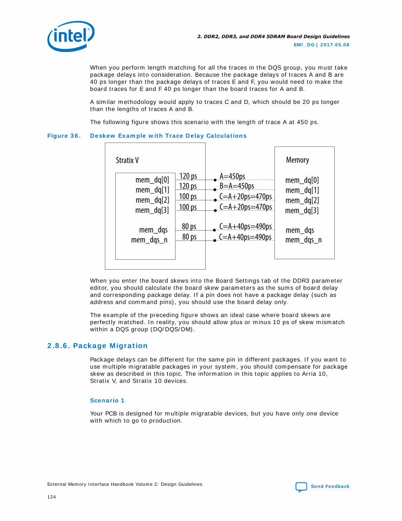
When you perform length matching for all the traces in the DQS group, you must takepackage delays into consideration. Because the package delays of traces A and B are40 ps longer than the package delays of traces E and F, you would need to make theboard traces for E and F 40 ps longer than the board traces for A and B.
A similar methodology would apply to traces C and D, which should be 20 ps longerthan the lengths of traces A and B.
The following figure shows this scenario with the length of trace A at 450 ps.
Figure 36. Deskew Example with Trace Delay Calculations
Stratix V
mem_dq[0]mem_dq[1]mem_dq[2]mem_dq[3]
mem_dqsmem_dqs_n
mem_dq[0]mem_dq[1]mem_dq[2]mem_dq[3]
mem_dqsmem_dqs_n
Memory
120 ps120 ps100 ps100 ps
80 ps80 ps
A=450psB=A=450psC=A+20ps=470psC=A+20ps=470ps
C=A+40ps=490psC=A+40ps=490ps
When you enter the board skews into the Board Settings tab of the DDR3 parametereditor, you should calculate the board skew parameters as the sums of board delayand corresponding package delay. If a pin does not have a package delay (such asaddress and command pins), you should use the board delay only.
The example of the preceding figure shows an ideal case where board skews areperfectly matched. In reality, you should allow plus or minus 10 ps of skew mismatchwithin a DQS group (DQ/DQS/DM).
2.8.6. Package Migration
Package delays can be different for the same pin in different packages. If you want touse multiple migratable packages in your system, you should compensate for packageskew as described in this topic. The information in this topic applies to Arria 10,Stratix V, and Stratix 10 devices.
Scenario 1
Your PCB is designed for multiple migratable devices, but you have only one devicewith which to go to production.
2. DDR2, DDR3, and DDR4 SDRAM Board Design Guidelines
EMI_DG | 2017.05.08
External Memory Interface Handbook Volume 2: Design Guidelines Send Feedback
124
Assume two migratable packages, device A and device B, and that you want to go toproduction with device A. Follow these steps:
1. Perform package deskew for device A.
2. Compile your design for device A, with the Package Skew option enabled.
3. Note the skews in the <core_name>.pin file for device A. Deskew these packageskews with board trace lengths as described in the preceding examples.
4. Recompile your design for device A.
5. For device B, open the parameter editor and deselect the Package Deskewoption.
6. Calculate board skew parameters, only taking into account the board traces fordevice B, and enter that value into the parameter editor for device B.
7. Regenerate the IP and recompile the design for device B.
8. Verify that timing requirements are met for both device A and device B.
Scenario 2
Your PCB is designed for multiple migratable devices, and you want to go toproduction with all of them.
Assume you have device A and device B, and plan to use both devices in production.Follow these steps:
1. Do not perform any package deskew compensation for either device.
2. Compile a Quartus Prime design for device A with the Package Deskew optiondisabled, and ensure that all board skews are entered accurately.
3. Verify that the Report DDR timing report meets your timing requirements.
4. Compile a Quartus Prime design for device B with the Package Deskew optiondisabled, and ensure that all board skews are entered accurately.
5. Verify that the Report DDR timing report meets your timing requirements.
2.8.7. Package Deskew for RLDRAM II and RLDRAM 3
You should follow Intel's package deskew guidance if you are using Arria 10, Stratix10, or Stratix V devices.
For more information on package deskew, refer to Package Deskew.
Related Information
Package Deskew
2.9. Document Revision History
2. DDR2, DDR3, and DDR4 SDRAM Board Design Guidelines
EMI_DG | 2017.05.08
Send Feedback External Memory Interface Handbook Volume 2: Design Guidelines
125
Date Version Changes
May 2017 2017.05.08 • Added Channel Signal Integrity Measurement section.• Added Stratix 10 to several sections.• Removed QDR-IV future support note from Package Deskew
Recommendations for Arria 10 and Stratix 10 Devices section.• Rebranded as Intel.
October 2016 2016.10.31 Maintenance release.
May 2016 2016.05.02 • Minor change to Clock Routing description in the DDR2 SDRAM LayoutGuidelines table in Layout Guidelines for DDR2 SDRAM Interface.
• Added maximum length of the first SDRAM to the last SDRAM for clockrouting and address and command routing for DDR4, in Layout Guidelinesfor DDR3 and DDR4 SDRAM Interfaces.
• Removed DRAM Termination Guidance from Layout Guidelines for DDR3and DDR4 SDRAM Interfaces.
• Added DDR4 support to Length Matching Rules.
November 2015 2015.11.02 • Minor additions to procedure steps in DQ/DQS/DM Deskew and Addressand Command Deskew.
• Added reference to Micron Technical Note in Layout Guidelines for DDR3and DDR4 SDRAM Interfaces.
• Changed title of Board Termination for DDR2 SDRAM to Termination forDDR2 SDRAM and Board Termination for DDR3 SDRAM to Termination forDDR3 SDRAM.
• Changed title of Leveling and Dynamic ODT to Leveling and DynamicTermination.
• Added DDR4 support in Dynamic ODT.• Removed topics pertaining to older device families.• Changed instances of Quartus II to Quartus Prime.
May 2015 2015.05.04 Maintenance release.
December 2014 2014.12.15 • Added MAX 10 to On-Chip Termination topic.• Added MAX 10 to Termination Recommendations table in Recommended
Termination Schemes topic.
August 2014 2014.08.15 • Added Arria V Soc and Cyclone V SoC devices to note in Leveling andDynamic ODT section.
• Added DDR4 to Read and Write Leveling section.• Revised text in On-Chip Termination section.• Added text to note in Board Termination for DDR3 SDRAM section.• Added Layout Approach information in the DDR3 and DDR4 on Arria 10
Devices section.• Recast expressions of length-matching measurements throughout DDR2
SDRAM Layout Guidelines table.• Made several changes to DDR3 and DDR4 SDRAM Layout Guidelines table:
— Added Spacing Guidelines section.— Removed millimeter approximations from lengths expressed in
picoseconds.— Revised Guidelines for Clock Routing, Address and Command Routing,
and DQ, DM, and DQS Routing Rules sections.• Added Spacing Guidelines information to Design Layout Guidelines
section.
December 2013 2013.12.16 • Review and minor updates of content.• Consolidated General Layout Guidelines.• Added DDR3 and DDR4 information for Arria 10 devices.• Updated chapter title to include DDR4 support.• Removed references to ALTMEMPHY.
continued...
2. DDR2, DDR3, and DDR4 SDRAM Board Design Guidelines
EMI_DG | 2017.05.08
External Memory Interface Handbook Volume 2: Design Guidelines Send Feedback
126
Date Version Changes
• Removed references to Cyclone III and Cyclone IV devices.• Removed references to Stratix II devices.• Corrected Vtt to Vdd in Memory Clocks for DDR3 SDRAM UDIMM section.
November 2012 5.0 • Updated Layout Guidelines for DDR2 SDRAM Interface and LayoutGuidelines for DDR3 SDRAM Interface.
• Added LRDIMM support.• Added Package Deskew section.
June 2012 4.1 Added Feedback icon.
November 2011 4.0 Added Arria V and Cyclone V information.
June 2011 3.0 • Merged DDR2 and DDR3 chapters to DDR2 and DDR3 SDRAM InterfaceTermination and Layout Guidelines and updated with leveling information.
• Added Stratix V information.
December 2010 2.1 Added DDR3 SDRAM Interface Termination, Drive Strength, Loading, andBoard Layout Guidelines chapter with Stratix V information.
July 2010 2.0 Updated Arria II GX information.
April 2010 1.0 Initial release.
2. DDR2, DDR3, and DDR4 SDRAM Board Design Guidelines
EMI_DG | 2017.05.08
Send Feedback External Memory Interface Handbook Volume 2: Design Guidelines
127
3. Dual-DIMM DDR2 and DDR3 SDRAM Board DesignGuidelines
The following topics describe guidelines for implementing dual unbuffered DIMM(UDIMM) DDR2 and DDR3 SDRAM interfaces.
The following topics discuss the impact on signal integrity of the data signal with thefollowing conditions in a dual-DIMM configuration:
• Populating just one slot versus populating both slots
• Populating slot 1 versus slot 2 when only one DIMM is used
• On-die termination (ODT) setting of 75-ohm versus an ODT setting of 150-ohm
For detailed information about a single-DIMM DDR2 SDRAM interface, refer to theDDR2 and DDR3 SDRAM Board Design Guidelines chapter.
Related Information
DDR2, DDR3, and DDR4 SDRAM Board Design Guidelines on page 81
3.1. General Layout Guidelines
The following table lists general board design layout guidelines. These guidelines areIntel recommendations, and should not be considered as hard requirements. Youshould perform signal integrity simulation on all the traces to verify the signal integrityof the interface. You should extract the slew rate and propagation delay information,enter it into the IP and compile the design to ensure that timing requirements aremet.
EMI_DG | 2017.05.08
Send Feedback
Intel Corporation. All rights reserved. Intel, the Intel logo, Altera, Arria, Cyclone, Enpirion, MAX, Nios, Quartusand Stratix words and logos are trademarks of Intel Corporation or its subsidiaries in the U.S. and/or othercountries. Intel warrants performance of its FPGA and semiconductor products to current specifications inaccordance with Intel's standard warranty, but reserves the right to make changes to any products and servicesat any time without notice. Intel assumes no responsibility or liability arising out of the application or use of anyinformation, product, or service described herein except as expressly agreed to in writing by Intel. Intelcustomers are advised to obtain the latest version of device specifications before relying on any publishedinformation and before placing orders for products or services.*Other names and brands may be claimed as the property of others.
ISO9001:2015Registered
Table 35. General Layout Guidelines
Parameter Guidelines
Impedance • All unused via pads must be removed, because they cause unwantedcapacitance.
• Trace impedance plays an important role in the signal integrity. You mustperform board level simulation to determine the best characteristic impedancefor your PCB. For example, it is possible that for multi rank systems 40 ohmscould yield better results than a traditional 50 ohm characteristic impedance.
Decoupling Parameter • Use 0.1 uF in 0402 size to minimize inductance• Make VTT voltage decoupling close to termination resistors• Connect decoupling caps between VTT and ground• Use a 0.1 uF cap for every other VTT pin and 0.01 uF cap for every VDD and
VDDQ pin• Verify the capacitive decoupling using the Intel Power Distribution Network
Design Tool
Power • Route GND and VCC as planes• Route VCCIO for memories in a single split plane with at least a 20-mil
(0.020 inches, or 0.508 mm) gap of separation• Route VTT as islands or 250-mil (6.35-mm) power traces• Route oscillators and PLL power as islands or 100-mil (2.54-mm) power traces
General Routing All specified delay matching requirements include PCB trace delays, different layerpropagation velocity variance, and crosstalk. To minimize PCB layer propogationvariance, Intel recommends that signals from the same net group always berouted on the same layer.• Use 45° angles (not 90° corners)• Avoid T-Junctions for critical nets or clocks• Avoid T-junctions greater than 250 mils (6.35 mm)• Disallow signals across split planes• Restrict routing other signals close to system reset signals• Avoid routing memory signals closer than 0.025 inch (0.635 mm) to PCI or
system clocks
Related Information
Power Distribution Network Design Tool
3.2. Dual-Slot Unbuffered DDR2 SDRAM
This topic describes guidelines for implementing a dual slot unbuffered DDR2 SDRAMinterface, operating at up to 400-MHz and 800-Mbps data rates.
The following figure shows a typical DQS, DQ, and DM signal topology for a dual-DIMMinterface configuration using the ODT feature of the DDR2 SDRAM components.
3. Dual-DIMM DDR2 and DDR3 SDRAM Board Design Guidelines
EMI_DG | 2017.05.08
Send Feedback External Memory Interface Handbook Volume 2: Design Guidelines
129
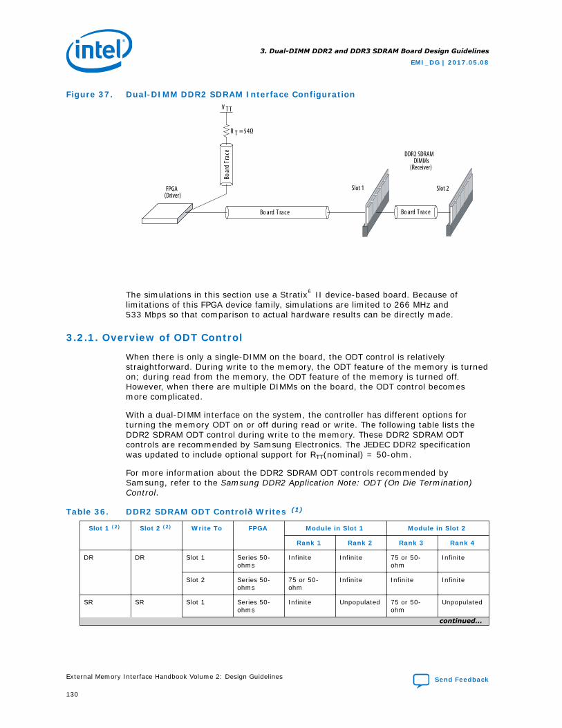
Figure 37. Dual-DIMM DDR2 SDRAM Interface Configuration
Bo ard T rac e
Boar
dTr
ace
V T T
R T =54Ω
Bo ard T rac e
Slot 1 Slot 2
DDR2 SDRAMDIMMs
(Receiver)
FPGA(Driver)
The simulations in this section use a Stratix® II device-based board. Because oflimitations of this FPGA device family, simulations are limited to 266 MHz and533 Mbps so that comparison to actual hardware results can be directly made.
3.2.1. Overview of ODT Control
When there is only a single-DIMM on the board, the ODT control is relativelystraightforward. During write to the memory, the ODT feature of the memory is turnedon; during read from the memory, the ODT feature of the memory is turned off.However, when there are multiple DIMMs on the board, the ODT control becomesmore complicated.
With a dual-DIMM interface on the system, the controller has different options forturning the memory ODT on or off during read or write. The following table lists theDDR2 SDRAM ODT control during write to the memory. These DDR2 SDRAM ODTcontrols are recommended by Samsung Electronics. The JEDEC DDR2 specificationwas updated to include optional support for RTT(nominal) = 50-ohm.
For more information about the DDR2 SDRAM ODT controls recommended bySamsung, refer to the Samsung DDR2 Application Note: ODT (On Die Termination)Control.
Table 36. DDR2 SDRAM ODT Control—Writes (1)
Slot 1 (2) Slot 2 (2) Write To FPGA Module in Slot 1 Module in Slot 2
Rank 1 Rank 2 Rank 3 Rank 4
DR DR Slot 1 Series 50-ohms
Infinite Infinite 75 or 50-ohm
Infinite
Slot 2 Series 50-ohms
75 or 50-ohm
Infinite Infinite Infinite
SR SR Slot 1 Series 50-ohms
Infinite Unpopulated 75 or 50-ohm
Unpopulated
continued...
3. Dual-DIMM DDR2 and DDR3 SDRAM Board Design Guidelines
EMI_DG | 2017.05.08
External Memory Interface Handbook Volume 2: Design Guidelines Send Feedback
130
Slot 1 (2) Slot 2 (2) Write To FPGA Module in Slot 1 Module in Slot 2
Rank 1 Rank 2 Rank 3 Rank 4
Slot 2 Series 50-ohms
75 or 50-ohm
Unpopulated Infinite Unpopulated
DR Empty Slot 1 Series 50-ohms
150-ohm Infinite Unpopulated Unpopulated
Empty DR Slot 2 Series 50-ohms
Unpopulated Unpopulated 150-ohm Infinite
SR Empty Slot 1 Series 50-ohms
150-ohm Unpopulated Unpopulated Unpopulated
Empty SR Slot 2 Series 50-ohms
Unpopulated Unpopulated 150-ohm Unpopulated
Notes to Table:1. For DDR2 at 400 MHz and 533 Mbps = 75-ohm; for DDR2 at 667 MHz and 800 Mbps = 50-ohm.2. SR = single ranked; DR = dual ranked.
Table 37. DDR2 SDRAM ODT Control—Reads (1)
Slot 1 (2) Slot 2 (2) Read From FPGA Module in Slot 1 Module in Slot 2
Rank 1 Rank 2 Rank 3 Rank 4
DR DR Slot 1 Parallel 50-ohms
Infinite Infinite 75 or 50-ohm
Infinite
Slot 2 Parallel 50-ohms
75 or 50-ohm
Infinite Infinite Infinite
SR SR Slot 1 Parallel 50-ohms
Infinite Unpopulated 75 or 50-ohm
Unpopulated
Slot 2 Parallel 50-ohms
75 or 50-ohm
Unpopulated Infinite Unpopulated
DR Empty Slot 1 Parallel 50-ohms
Infinite Infinite Unpopulated Unpopulated
Empty DR Slot 2 Parallel 50-ohms
Unpopulated Unpopulated Infinite Infinite
SR Empty Slot 1 Parallel 50-ohms
Infinite Unpopulated Unpopulated Unpopulated
Empty SR Slot 2 Parallel 50-ohms
Unpopulated Unpopulated Infinite Unpopulated
Notes to Table:1. For DDR2 at 400 MHz and 533 Mbps = 75-ohm; for DDR2 at 667 MHz and 800 Mbps = 50-ohm.2. SR = single ranked; DR = dual ranked.
3.2.2. DIMM Configuration
Although populating both memory slots is common in a dual-DIMM memory system,there are some instances when only one slot is populated.
For example, some systems are designed to have a certain amount of memory initiallyand as applications get more complex, the system can be easily upgraded toaccommodate more memory by populating the second memory slot without re-designing the system. The following topics discuss a dual-DIMM system where the
3. Dual-DIMM DDR2 and DDR3 SDRAM Board Design Guidelines
EMI_DG | 2017.05.08
Send Feedback External Memory Interface Handbook Volume 2: Design Guidelines
131
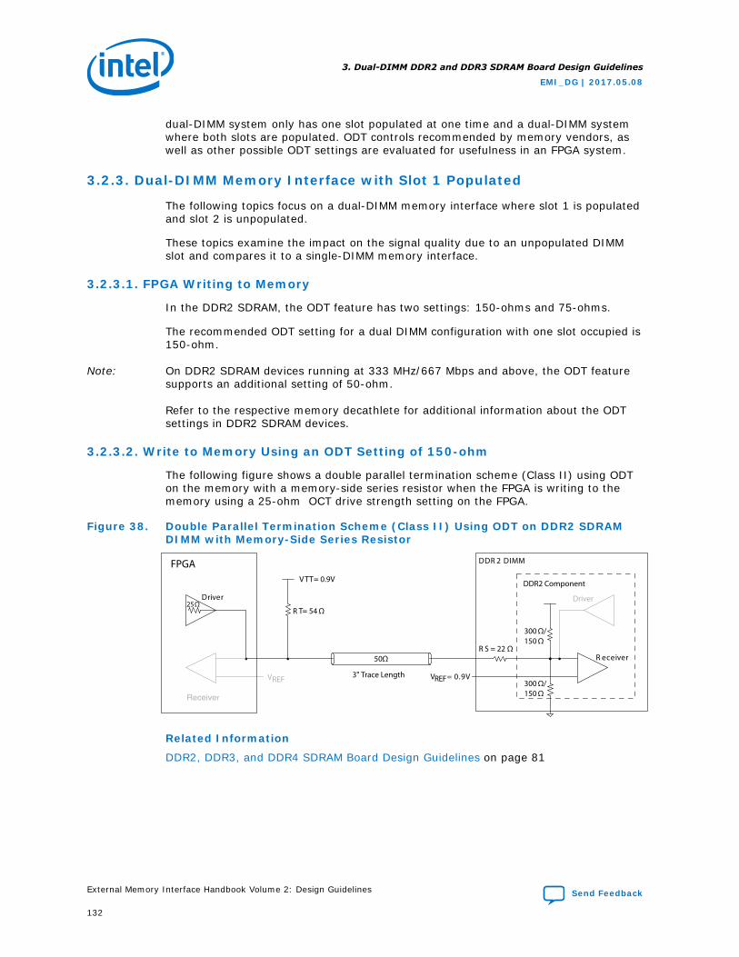
dual-DIMM system only has one slot populated at one time and a dual-DIMM systemwhere both slots are populated. ODT controls recommended by memory vendors, aswell as other possible ODT settings are evaluated for usefulness in an FPGA system.
3.2.3. Dual-DIMM Memory Interface with Slot 1 Populated
The following topics focus on a dual-DIMM memory interface where slot 1 is populatedand slot 2 is unpopulated.
These topics examine the impact on the signal quality due to an unpopulated DIMMslot and compares it to a single-DIMM memory interface.
3.2.3.1. FPGA Writing to Memory
In the DDR2 SDRAM, the ODT feature has two settings: 150-ohms and 75-ohms.
The recommended ODT setting for a dual DIMM configuration with one slot occupied is150-ohm.
Note: On DDR2 SDRAM devices running at 333 MHz/667 Mbps and above, the ODT featuresupports an additional setting of 50-ohm.
Refer to the respective memory decathlete for additional information about the ODTsettings in DDR2 SDRAM devices.
3.2.3.2. Write to Memory Using an ODT Setting of 150-ohm
The following figure shows a double parallel termination scheme (Class II) using ODTon the memory with a memory-side series resistor when the FPGA is writing to thememory using a 25-ohm OCT drive strength setting on the FPGA.
Figure 38. Double Parallel Termination Scheme (Class II) Using ODT on DDR2 SDRAMDIMM with Memory-Side Series Resistor
Driver
FPGA
VREF= 0.9V
R eceiver
DDR 2 DIMM
25 Ω
300 Ω/150 Ω
300 Ω/150 Ω
R T= 54 Ω
50 Ω
V TT = 0.9V
3" Trace Length
R S = 22 Ω
DDR2 Component
r
VREF
Driver
Related Information
DDR2, DDR3, and DDR4 SDRAM Board Design Guidelines on page 81
3. Dual-DIMM DDR2 and DDR3 SDRAM Board Design Guidelines
EMI_DG | 2017.05.08
External Memory Interface Handbook Volume 2: Design Guidelines Send Feedback
132
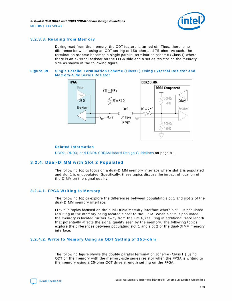
3.2.3.3. Reading from Memory
During read from the memory, the ODT feature is turned off. Thus, there is nodifference between using an ODT setting of 150-ohm and 75-ohm. As such, thetermination scheme becomes a single parallel termination scheme (Class I) wherethere is an external resistor on the FPGA side and a series resistor on the memoryside as shown in the following figure.
Figure 39. Single Parallel Termination Scheme (Class I) Using External Resistor andMemory-Side Series Resistor
FPGA
VTT = 0.9 V
25 Ω
Driver
Receiver
VREF = 0.9 V
RT = 54 Ω
50 Ω
DDR2 DIMM
Driver
ReceiverRS = 22 Ω
300 Ω/150 Ω
300 Ω/150 Ω
VREF
DDR2 Component
3” TraceLength
Related Information
DDR2, DDR3, and DDR4 SDRAM Board Design Guidelines on page 81
3.2.4. Dual-DIMM with Slot 2 Populated
The following topics focus on a dual-DIMM memory interface where slot 2 is populatedand slot 1 is unpopulated. Specifically, these topics discuss the impact of location ofthe DIMM on the signal quality.
3.2.4.1. FPGA Writing to Memory
The following topics explore the differences between populating slot 1 and slot 2 of thedual-DIMM memory interface.
Previous topics focused on the dual-DIMM memory interface where slot 1 is populatedresulting in the memory being located closer to the FPGA. When slot 2 is populated,the memory is located further away from the FPGA, resulting in additional trace lengththat potentially affects the signal quality seen by the memory. The following topicsexplore the differences between populating slot 1 and slot 2 of the dual-DIMM memoryinterface.
3.2.4.2. Write to Memory Using an ODT Setting of 150-ohm
The following figure shows the double parallel termination scheme (Class II) usingODT on the memory with the memory-side series resistor when the FPGA is writing tothe memory using a 25-ohm OCT drive strength setting on the FPGA.
3. Dual-DIMM DDR2 and DDR3 SDRAM Board Design Guidelines
EMI_DG | 2017.05.08
Send Feedback External Memory Interface Handbook Volume 2: Design Guidelines
133
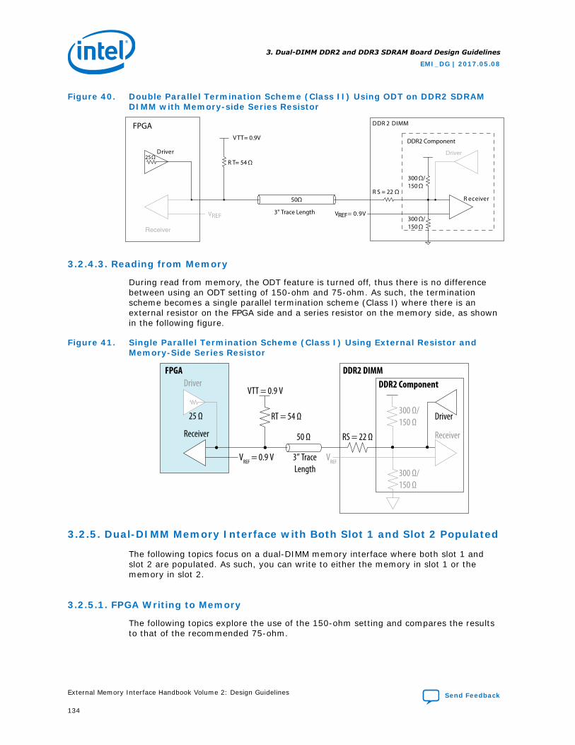
Figure 40. Double Parallel Termination Scheme (Class II) Using ODT on DDR2 SDRAMDIMM with Memory-side Series Resistor
Driver
FPGA
VREF= 0.9V
R eceiver
DDR 2 DIMM
25 Ω
300 Ω/150 Ω
300 Ω/150 Ω
R T= 54 Ω
50 Ω
V TT = 0.9V
3" Trace Length
R S = 22 Ω
DDR2 Component
r
VREF
Driver
3.2.4.3. Reading from Memory
During read from memory, the ODT feature is turned off, thus there is no differencebetween using an ODT setting of 150-ohm and 75-ohm. As such, the terminationscheme becomes a single parallel termination scheme (Class I) where there is anexternal resistor on the FPGA side and a series resistor on the memory side, as shownin the following figure.
Figure 41. Single Parallel Termination Scheme (Class I) Using External Resistor andMemory-Side Series Resistor
FPGA
VTT = 0.9 V
25 Ω
Driver
Receiver
VREF = 0.9 V
RT = 54 Ω
50 Ω
DDR2 DIMM
Driver
ReceiverRS = 22 Ω
300 Ω/150 Ω
300 Ω/150 Ω
VREF
DDR2 Component
3” TraceLength
3.2.5. Dual-DIMM Memory Interface with Both Slot 1 and Slot 2 Populated
The following topics focus on a dual-DIMM memory interface where both slot 1 andslot 2 are populated. As such, you can write to either the memory in slot 1 or thememory in slot 2.
3.2.5.1. FPGA Writing to Memory
The following topics explore the use of the 150-ohm setting and compares the resultsto that of the recommended 75-ohm.
3. Dual-DIMM DDR2 and DDR3 SDRAM Board Design Guidelines
EMI_DG | 2017.05.08
External Memory Interface Handbook Volume 2: Design Guidelines Send Feedback
134
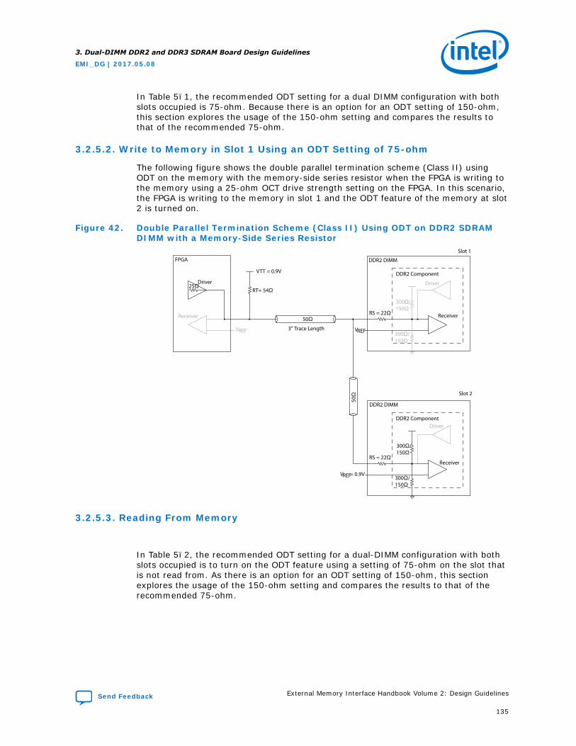
In Table 5–1, the recommended ODT setting for a dual DIMM configuration with bothslots occupied is 75-ohm. Because there is an option for an ODT setting of 150-ohm,this section explores the usage of the 150-ohm setting and compares the results tothat of the recommended 75-ohm.
3.2.5.2. Write to Memory in Slot 1 Using an ODT Setting of 75-ohm
The following figure shows the double parallel termination scheme (Class II) usingODT on the memory with the memory-side series resistor when the FPGA is writing tothe memory using a 25-ohm OCT drive strength setting on the FPGA. In this scenario,the FPGA is writing to the memory in slot 1 and the ODT feature of the memory at slot2 is turned on.
Figure 42. Double Parallel Termination Scheme (Class II) Using ODT on DDR2 SDRAMDIMM with a Memory-Side Series Resistor
Driver
FPGA DDR2 DIMM
25WRT= 54W
50W
VTT = 0.9V
3" Trace Length
RS = 22W
DDR2 Component
VREF
VREF
= 0.9V
Receiver
Receiver
DDR2 DIMM
300W/150W
300W/150W
RS = 22W
DDR2 Component
50W
Slot 1
Slot 2
Driver
Driver
Receiver
VREF
300W/150W
300W/150W
3.2.5.3. Reading From Memory
In Table 5–2, the recommended ODT setting for a dual-DIMM configuration with bothslots occupied is to turn on the ODT feature using a setting of 75-ohm on the slot thatis not read from. As there is an option for an ODT setting of 150-ohm, this sectionexplores the usage of the 150-ohm setting and compares the results to that of therecommended 75-ohm.
3. Dual-DIMM DDR2 and DDR3 SDRAM Board Design Guidelines
EMI_DG | 2017.05.08
Send Feedback External Memory Interface Handbook Volume 2: Design Guidelines
135
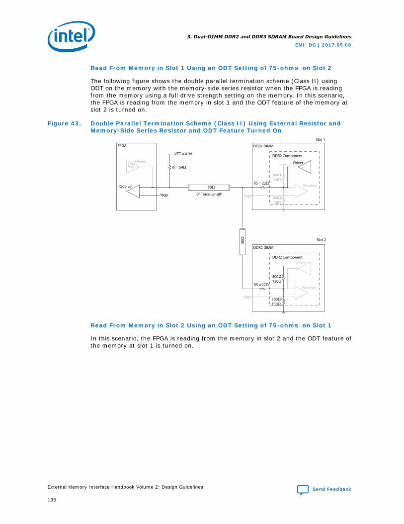
Read From Memory in Slot 1 Using an ODT Setting of 75-ohms on Slot 2
The following figure shows the double parallel termination scheme (Class II) usingODT on the memory with the memory-side series resistor when the FPGA is readingfrom the memory using a full drive strength setting on the memory. In this scenario,the FPGA is reading from the memory in slot 1 and the ODT feature of the memory atslot 2 is turned on.
Figure 43. Double Parallel Termination Scheme (Class II) Using External Resistor andMemory-Side Series Resistor and ODT Feature Turned On
Receiver
FPGA
Driver
DDR2 DIMM
VREF
300W/150W
RT= 54W
50W
VTT = 0.9V
3" Trace Length
RS = 22W
DDR2 Component
DDR2 DIMM
300W/150W
300W/150W
RS = 22W
DDR2 Component
50W
Slot 1
Slot 2
Driver
300W/150W
Driver
Receiver
Receiver
25W
VREF
VREF
Read From Memory in Slot 2 Using an ODT Setting of 75-ohms on Slot 1
In this scenario, the FPGA is reading from the memory in slot 2 and the ODT feature ofthe memory at slot 1 is turned on.
3. Dual-DIMM DDR2 and DDR3 SDRAM Board Design Guidelines
EMI_DG | 2017.05.08
External Memory Interface Handbook Volume 2: Design Guidelines Send Feedback
136
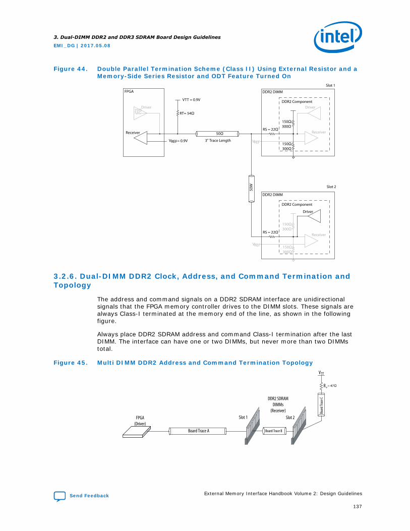
Figure 44. Double Parallel Termination Scheme (Class II) Using External Resistor and aMemory-Side Series Resistor and ODT Feature Turned On
Receiver
FPGA
VREF
DDR2 DIMM
VREF
25W
150W/300W
150W/300W
RT= 54W
50W
VTT = 0.9V
3" Trace Length
RS = 22W
DDR2 Component
VREF
Driver
DDR2 DIMM
RS = 22W
DDR2 Component
50W
Slot 1
Slot 2
= 0.9V
Driver Driver
Receiver
Receiver
150W/300W
150W/300W
3.2.6. Dual-DIMM DDR2 Clock, Address, and Command Termination andTopology
The address and command signals on a DDR2 SDRAM interface are unidirectionalsignals that the FPGA memory controller drives to the DIMM slots. These signals arealways Class-I terminated at the memory end of the line, as shown in the followingfigure.
Always place DDR2 SDRAM address and command Class-I termination after the lastDIMM. The interface can have one or two DIMMs, but never more than two DIMMstotal.
Figure 45. Multi DIMM DDR2 Address and Command Termination Topology
Board Trace A
Boar
d Tra
ce C
VTT
R PW
Board Trace B
Slot 1 Slot 2
DDR2 SDRAMDIMMs
(Receiver)FPGA
(Driver)
= 47
3. Dual-DIMM DDR2 and DDR3 SDRAM Board Design Guidelines
EMI_DG | 2017.05.08
Send Feedback External Memory Interface Handbook Volume 2: Design Guidelines
137

In the above figure, observe the following points:
• Board trace A = 1.9 to 4.5 inches (48 to 115 mm)
• Board trace B = 0.425 inches (10.795 mm)
• Board trace C = 0.2 to 0.55 inches (5 to 13 mm)
• Total of board trace A + B + C = 2.5 to 5 inches (63 to 127 mm)
• RP = 36 to 56-ohm
• Length match all address and command signals to +250 mils (+5 mm) or +/– 50ps of memory clock length at the DIMM.
You may place a compensation capacitor directly before the first DIMM slot 1 toimprove signal quality on the address and command signal group. If you fit acapacitor, Intel recommends a value of 24 pF.
For more information, refer to Micron TN47-01.
3.2.7. Control Group Signals
The control group of signals: chip select CS#, clock enable CKE, and ODT are always1T regardless of whether you implement a full-rate or half-rate design.
As the signals are also SDR, the control group signals operate at a maximumfrequency of 0.5 × the data rate. For example, in a 400-MHz design, the maximumcontrol group frequency is 200 MHz.
3.2.8. Clock Group Signals
Depending on the specific form factor, DDR2 SDRAM DIMMs have two or threedifferential clock pairs, to ensure that the loading on the clock signals is not excessive.The clock signals are always terminated on the DIMMs and hence no termination isrequired on your PCB.
Additionally, each DIMM slot is required to have its own dedicated set of clock signals.Hence clock signals are always point-to-point from the FPGA PHY to each individualDIMM slot. Individual memory clock signals should never be shared between twoDIMM slots.
A typical two slot DDR2 DIMM design therefore has six differential memory clock pairs—three to the first DIMM and three to the second DIMM. All six memory clock pairsmust be delay matched to each other to ±25 mils (±0.635 mm) and ±10 mils(±0.254 mm) for each CLK to CLK# signal.
You may place a compensation capacitor between each clock pair directly before theDIMM connector, to improve the clock slew rates. As FPGA devices have fullyprogrammable drive strength and slew rate options, this capacitor is usually notrequired for FPGA design. However, Intel advises that you simulate your specificimplementation to ascertain if this capacitor is required or not. If fitted the best valueis typically 5 pF.
3.3. Dual-Slot Unbuffered DDR3 SDRAM
The following topics detail the system implementation of a dual slot unbuffered DDR3SDRAM interface, operating at up to 400 MHz and 800 Mbps data rates.
3. Dual-DIMM DDR2 and DDR3 SDRAM Board Design Guidelines
EMI_DG | 2017.05.08
External Memory Interface Handbook Volume 2: Design Guidelines Send Feedback
138
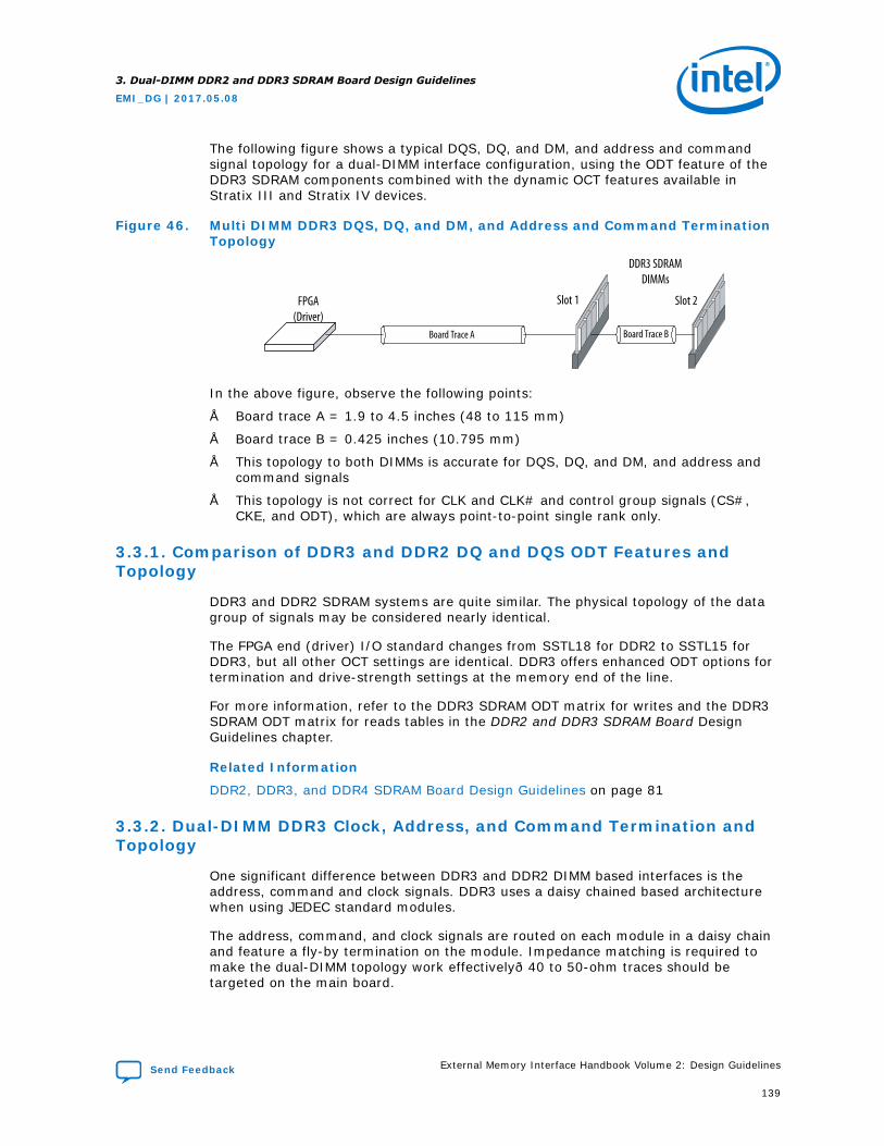
The following figure shows a typical DQS, DQ, and DM, and address and commandsignal topology for a dual-DIMM interface configuration, using the ODT feature of theDDR3 SDRAM components combined with the dynamic OCT features available inStratix III and Stratix IV devices.
Figure 46. Multi DIMM DDR3 DQS, DQ, and DM, and Address and Command TerminationTopology
Board Trace A
Board Trace B
Slot 1 Slot 2
DDR3 SDRAMDIMMs
FPGA(Driver)
In the above figure, observe the following points:
• Board trace A = 1.9 to 4.5 inches (48 to 115 mm)
• Board trace B = 0.425 inches (10.795 mm)
• This topology to both DIMMs is accurate for DQS, DQ, and DM, and address andcommand signals
• This topology is not correct for CLK and CLK# and control group signals (CS#,CKE, and ODT), which are always point-to-point single rank only.
3.3.1. Comparison of DDR3 and DDR2 DQ and DQS ODT Features andTopology
DDR3 and DDR2 SDRAM systems are quite similar. The physical topology of the datagroup of signals may be considered nearly identical.
The FPGA end (driver) I/O standard changes from SSTL18 for DDR2 to SSTL15 forDDR3, but all other OCT settings are identical. DDR3 offers enhanced ODT options fortermination and drive-strength settings at the memory end of the line.
For more information, refer to the DDR3 SDRAM ODT matrix for writes and the DDR3SDRAM ODT matrix for reads tables in the DDR2 and DDR3 SDRAM Board DesignGuidelines chapter.
Related Information
DDR2, DDR3, and DDR4 SDRAM Board Design Guidelines on page 81
3.3.2. Dual-DIMM DDR3 Clock, Address, and Command Termination andTopology
One significant difference between DDR3 and DDR2 DIMM based interfaces is theaddress, command and clock signals. DDR3 uses a daisy chained based architecturewhen using JEDEC standard modules.
The address, command, and clock signals are routed on each module in a daisy chainand feature a fly-by termination on the module. Impedance matching is required tomake the dual-DIMM topology work effectively—40 to 50-ohm traces should betargeted on the main board.
3. Dual-DIMM DDR2 and DDR3 SDRAM Board Design Guidelines
EMI_DG | 2017.05.08
Send Feedback External Memory Interface Handbook Volume 2: Design Guidelines
139
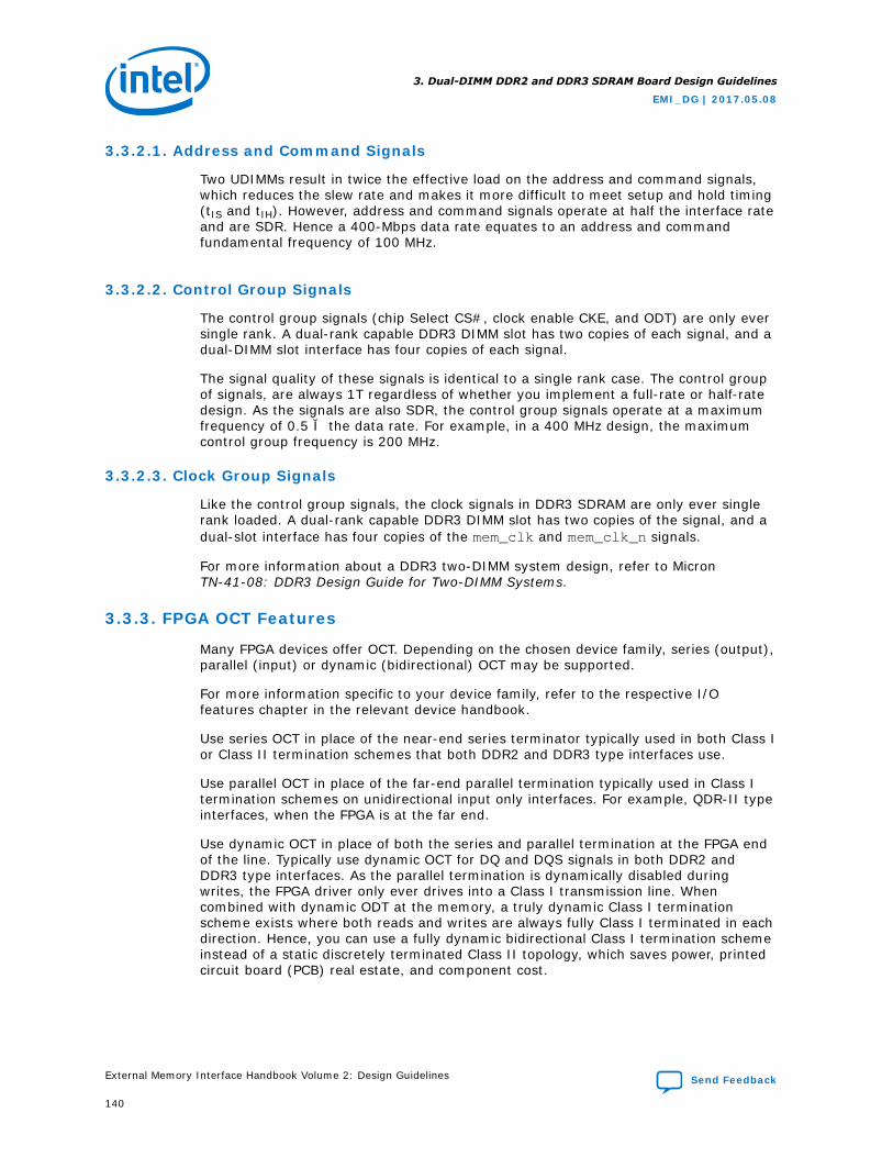
3.3.2.1. Address and Command Signals
Two UDIMMs result in twice the effective load on the address and command signals,which reduces the slew rate and makes it more difficult to meet setup and hold timing(tIS and tIH). However, address and command signals operate at half the interface rateand are SDR. Hence a 400-Mbps data rate equates to an address and commandfundamental frequency of 100 MHz.
3.3.2.2. Control Group Signals
The control group signals (chip Select CS#, clock enable CKE, and ODT) are only eversingle rank. A dual-rank capable DDR3 DIMM slot has two copies of each signal, and adual-DIMM slot interface has four copies of each signal.
The signal quality of these signals is identical to a single rank case. The control groupof signals, are always 1T regardless of whether you implement a full-rate or half-ratedesign. As the signals are also SDR, the control group signals operate at a maximumfrequency of 0.5 × the data rate. For example, in a 400 MHz design, the maximumcontrol group frequency is 200 MHz.
3.3.2.3. Clock Group Signals
Like the control group signals, the clock signals in DDR3 SDRAM are only ever singlerank loaded. A dual-rank capable DDR3 DIMM slot has two copies of the signal, and adual-slot interface has four copies of the mem_clk and mem_clk_n signals.
For more information about a DDR3 two-DIMM system design, refer to MicronTN-41-08: DDR3 Design Guide for Two-DIMM Systems.
3.3.3. FPGA OCT Features
Many FPGA devices offer OCT. Depending on the chosen device family, series (output),parallel (input) or dynamic (bidirectional) OCT may be supported.
For more information specific to your device family, refer to the respective I/Ofeatures chapter in the relevant device handbook.
Use series OCT in place of the near-end series terminator typically used in both Class Ior Class II termination schemes that both DDR2 and DDR3 type interfaces use.
Use parallel OCT in place of the far-end parallel termination typically used in Class Itermination schemes on unidirectional input only interfaces. For example, QDR-II typeinterfaces, when the FPGA is at the far end.
Use dynamic OCT in place of both the series and parallel termination at the FPGA endof the line. Typically use dynamic OCT for DQ and DQS signals in both DDR2 andDDR3 type interfaces. As the parallel termination is dynamically disabled duringwrites, the FPGA driver only ever drives into a Class I transmission line. Whencombined with dynamic ODT at the memory, a truly dynamic Class I terminationscheme exists where both reads and writes are always fully Class I terminated in eachdirection. Hence, you can use a fully dynamic bidirectional Class I termination schemeinstead of a static discretely terminated Class II topology, which saves power, printedcircuit board (PCB) real estate, and component cost.
3. Dual-DIMM DDR2 and DDR3 SDRAM Board Design Guidelines
EMI_DG | 2017.05.08
External Memory Interface Handbook Volume 2: Design Guidelines Send Feedback
140
3.3.3.1. Arria V, Cyclone V, Stratix III, Stratix IV, and Stratix V Devices
Arria® V, Cyclone® V, Stratix III, Stratix IV, and Stratix V devices feature full dynamicOCT termination capability, Intel advises that you use this feature combined with theSDRAM ODT to simplify PCB layout and save power.
3.3.3.2. Arria II GX Devices
Arria II GX devices do not support dynamic OCT. Intel recommends that you useseries OCT with SDRAM ODT. Use parallel discrete termination at the FPGA end of theline when necessary.
For more information, refer to the DDR2 and DDR3 SDRAM Board Design Guidelineschapter.
Related Information
DDR2, DDR3, and DDR4 SDRAM Board Design Guidelines on page 81
3.4. Document Revision History
Date Version Changes
May 2017 2017.5.08 Rebranded as Intel.
October 2016 2016.10.31 Maintenance release.
May 2016 2016.05.02 Maintenance release.
November 2015 2015.11.02 Maintenance release.
May 2015 2015.05.04 Maintenance release.
December 2014 2014.12.15 Maintenance release.
August 2014 2014.08.15 Removed Address and Command Signals section from Dual-DIMM DDR2Clock, Address, and Command Termination and Topology
December 2013 2013.12.16 • Reorganized content.• Consolidated General Layout Guidelines.• Removed references to ALTMEMPHY.• Removed references to Stratix II devices.
June 2012 4.1 Added Feedback icon.
November 2011 4.0 Added Arria V and Cyclone V information.
June 2011 3.0 Added Stratix V information.
December 2010 2.1 Maintenance update.
July 2010 2.0 Updated Arria II GX information.
April 2010 1.0 Initial release.
3. Dual-DIMM DDR2 and DDR3 SDRAM Board Design Guidelines
EMI_DG | 2017.05.08
Send Feedback External Memory Interface Handbook Volume 2: Design Guidelines
141
4. LPDDR2 and LPDDR3 SDRAM Board Design GuidelinesThe following topics provide guidelines to improve your system's signal integrity andto successfully implement an LPDDR2 or LPDDR3 SDRAM interface in your system.
4.1. LPDDR2 Guidance
The LPDDR2 SDRAM Controller with UniPHY intellectual property (IP) enables you toimplement LPDDR2 SDRAM interfaces with Arria® V and Cyclone® V devices.
The following topics focus on key factors that affect signal integrity:
• I/O standards
• LPDDR2 configurations
• Signal terminations
• Printed circuit board (PCB) layout guidelines
I/O Standards
LPDDR2 SDRAM interface signals use HSUL-12 JEDEC I/O signaling standards, whichprovide low power and low emissions. The HSUL-12 JEDEC I/O standard is mainly forpoint-to-point unterminated bus topology. This standard eliminates the need forexternal series or parallel termination resistors in LPDDR2 SDRAM implementation.With this standard, termination power is greatly reduced and programmable drivestrength is used to match the impedance.
To select the most appropriate standard for your interface, refer to the the DeviceDatasheet for Arria V Devices chapter in the Arria V Device Handbook, or the DeviceDatasheet for Cyclone V Devices chapter in the Cyclone V Device Handbook.
Related Information
• Arria V Device Datasheet
• Cyclone V Device Datasheet
4.1.1. LPDDR2 SDRAM Configurations
The LPDDR2 SDRAM Controller with UniPHY IP supports interfaces for LPDDR2 SDRAMwith a single device, and multiple devices up to a maximum width of 32 bits.
When using multiple devices, a balanced-T topology is recommended for the signalconnected from single point to multiple point, to maintain equal flight time.
You should connect a 200 ohm differential termination resistor between CK/CK# inmultiple device designs as shown in the second figure below, to maintain an effectiveresistance of 100 ohms.
EMI_DG | 2017.05.08
Send Feedback
Intel Corporation. All rights reserved. Intel, the Intel logo, Altera, Arria, Cyclone, Enpirion, MAX, Nios, Quartusand Stratix words and logos are trademarks of Intel Corporation or its subsidiaries in the U.S. and/or othercountries. Intel warrants performance of its FPGA and semiconductor products to current specifications inaccordance with Intel's standard warranty, but reserves the right to make changes to any products and servicesat any time without notice. Intel assumes no responsibility or liability arising out of the application or use of anyinformation, product, or service described herein except as expressly agreed to in writing by Intel. Intelcustomers are advised to obtain the latest version of device specifications before relying on any publishedinformation and before placing orders for products or services.*Other names and brands may be claimed as the property of others.
ISO9001:2015Registered
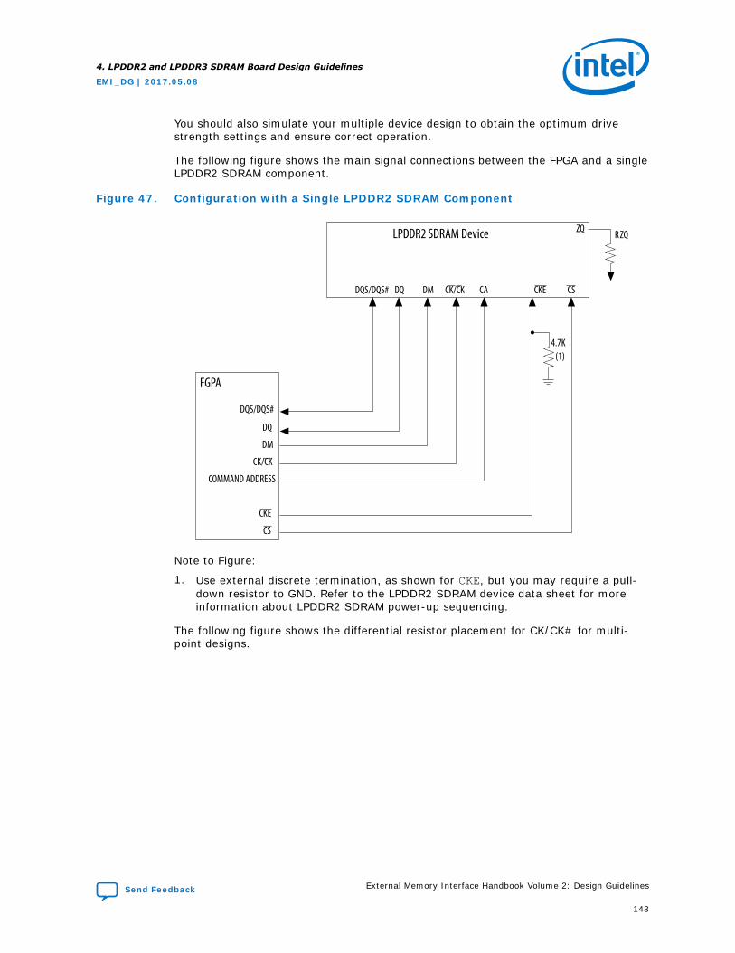
You should also simulate your multiple device design to obtain the optimum drivestrength settings and ensure correct operation.
The following figure shows the main signal connections between the FPGA and a singleLPDDR2 SDRAM component.
Figure 47. Configuration with a Single LPDDR2 SDRAM Component
FGPA
LPDDR2 SDRAM Device ZQ RZQ
DQ DM CK/CK CA CKE
DQ
DM
CK/CK
COMMAND ADDRESS
CKE
CS
DQS/DQS# CS
(1)
DQS/DQS#
4.7K
Note to Figure:
1. Use external discrete termination, as shown for CKE, but you may require a pull-down resistor to GND. Refer to the LPDDR2 SDRAM device data sheet for moreinformation about LPDDR2 SDRAM power-up sequencing.
The following figure shows the differential resistor placement for CK/CK# for multi-point designs.
4. LPDDR2 and LPDDR3 SDRAM Board Design Guidelines
EMI_DG | 2017.05.08
Send Feedback External Memory Interface Handbook Volume 2: Design Guidelines
143
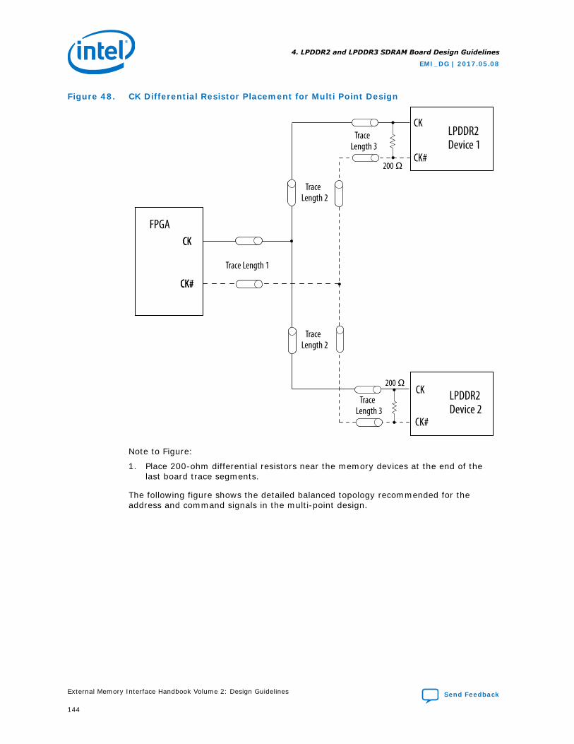
Figure 48. CK Differential Resistor Placement for Multi Point Design
FPGACK
CK#
LPDDR2Device 1
LPDDR2Device 2
CK
CK
CK
CK#
CK#
CK#
Trace Length 1
Trace Length 2
Trace Length 2
Trace Length 3
Trace Length 3
200 W
200 W
Note to Figure:
1. Place 200-ohm differential resistors near the memory devices at the end of thelast board trace segments.
The following figure shows the detailed balanced topology recommended for theaddress and command signals in the multi-point design.
4. LPDDR2 and LPDDR3 SDRAM Board Design Guidelines
EMI_DG | 2017.05.08
External Memory Interface Handbook Volume 2: Design Guidelines Send Feedback
144
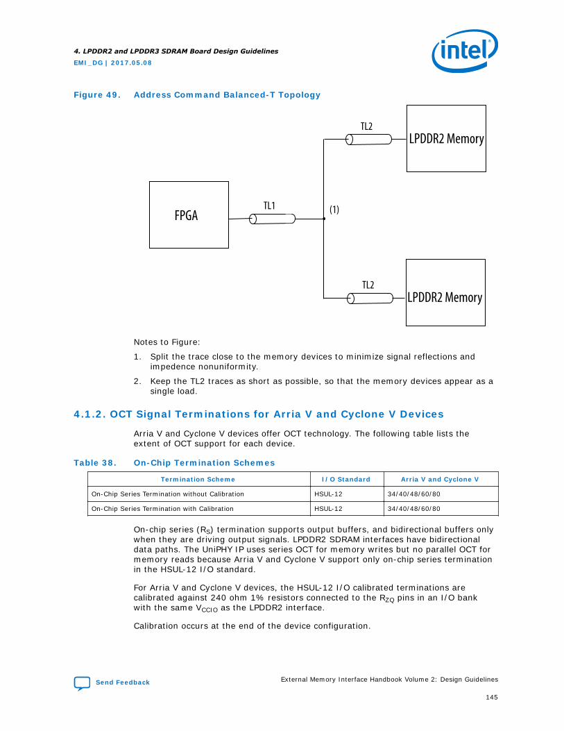
Figure 49. Address Command Balanced-T Topology
LPDDR2 Memory
LPDDR2 Memory
FPGA
TL2
TL1
TL2
. (1)
Notes to Figure:
1. Split the trace close to the memory devices to minimize signal reflections andimpedence nonuniformity.
2. Keep the TL2 traces as short as possible, so that the memory devices appear as asingle load.
4.1.2. OCT Signal Terminations for Arria V and Cyclone V Devices
Arria V and Cyclone V devices offer OCT technology. The following table lists theextent of OCT support for each device.
Table 38. On-Chip Termination Schemes
Termination Scheme I/O Standard Arria V and Cyclone V
On-Chip Series Termination without Calibration HSUL-12 34/40/48/60/80
On-Chip Series Termination with Calibration HSUL-12 34/40/48/60/80
On-chip series (RS) termination supports output buffers, and bidirectional buffers onlywhen they are driving output signals. LPDDR2 SDRAM interfaces have bidirectionaldata paths. The UniPHY IP uses series OCT for memory writes but no parallel OCT formemory reads because Arria V and Cyclone V support only on-chip series terminationin the HSUL-12 I/O standard.
For Arria V and Cyclone V devices, the HSUL-12 I/O calibrated terminations arecalibrated against 240 ohm 1% resistors connected to the RZQ pins in an I/O bankwith the same VCCIO as the LPDDR2 interface.
Calibration occurs at the end of the device configuration.
4. LPDDR2 and LPDDR3 SDRAM Board Design Guidelines
EMI_DG | 2017.05.08
Send Feedback External Memory Interface Handbook Volume 2: Design Guidelines
145
LPDDR2 SDRAM memory components have a ZQ pin which connects through a resistorRZQ (240 ohm) to ground. The output signal impedances for LPDDR2 SDRAM are34.3 ohm, 40 ohm, 48 ohm, 60 ohm, 80 ohm, and 120 ohm. The output signalimpedance is set by mode register during initialization. Refer to the LPDDR2 SDRAMdevice data sheet for more information.
For information about OCT, refer to the I/O Features in Arria V Devices chapter in theArria V Device Handbook, or the I/O Features in Cyclone V Devices chapter in theCyclone V Device Handbook.
The following section shows HyperLynx simulation eye diagrams to demonstrate signaltermination options. Intel strongly recommends signal terminations to optimize signalintegrity and timing margins, and to minimize unwanted emissions, reflections, andcrosstalk.
All of the eye diagrams shown in this section are for a 50 ohm trace with apropagation delay of 509 ps which is approximately a 2.8-inch trace on a standardFR4 PCB. The signal I/O standard is HSUL-12.
The eye diagrams in this section show the best case achievable and do not take intoaccount PCB vias, crosstalk, and other degrading effects such as variations in the PCBstructure due to manufacturing tolerances.
Note: Simulate your design to ensure correct operation.
Related Information
• I/O Features in Arria V Devices
• I/O Features in Cyclone V Devices
4.1.2.1. Outputs from the FPGA to the LPDDR2 Component
The following output signals are from the FPGA to the LPDDR2 SDRAM component:
• write data (DQ)
• data mask (DM)
• data strobe (DQS/DQS#)
• command address
• command (CS, and CKE)
• clocks (CK/CK#)
No far-end memory termination is needed when driving output signals from FPGA toLPDDR2 SDRAM. Cyclone V and Arria V devices offer the OCT series termination forimpedance matching.
4.1.2.2. Input to the FPGA from the LPDDR2 SDRAM Component
The LPDDR2 SDRAM component drives the following input signals into the FPGA:
• read data
• DQS
4. LPDDR2 and LPDDR3 SDRAM Board Design Guidelines
EMI_DG | 2017.05.08
External Memory Interface Handbook Volume 2: Design Guidelines Send Feedback
146
LPDDR2 SDRAM provides the flexibility to adjust drive strength to match theimpedance of the memory bus, eliminating the need for termination voltage (VTT) andseries termination resistors.
The programmable drive strength options are 34.3 ohms, 40 ohms (default), 48 ohms,60 ohms, 80 ohms, and 120 ohms. You must perform board simulation to determinethe best option for your board layout.
Note: By default, LPDDR2 SDRAM UniPHY IP uses 40 ohm drive strength.
4.1.2.3. Termination Schemes
The following table lists the recommended termination schemes for major LPDDR2SDRAM memory interface signals.
These signals include data (DQ), data strobe (DQS), data mask (DM), clocks (CK, andCK#), command address (CA), and control (CS#, and CKE).
Table 39. Termination Recommendations for Arria V and Cyclone V Devices
Signal Type HSUL-12 Standard (1) (2) Memory End Termination
DQS/DQS# R34 CAL ZQ40
Data (Write) R34 CAL –
Data (Read) – ZQ40
Data Mask (DM) R34 CAL –
CK/CK# Clocks R34 CAL ×1 = – (4)
×2 = 200 -ohmDifferential (5)
Command Address (CA), R34 CAL –
Chip Select (CS#) R34 CAL –
Clock Enable (CKE) (3) R34 CAL 4.7 K-ohmparallel to GND
Notes to Table:1. R is effective series output impedance.2. CAL is OCT with calibration.3. Intel recommends that you use a 4.7 K-ohmparallel to GND if your design meets the power sequencing requirements
of the LPDDR2 SDRAM component. Refer to the LPDDR2 SDRAM data sheet for further information.4. ×1 is a single-device load.5. ×2 is a double-device load. An alternative option is to use a 100 -ohm differential termination at the trace split.
Note: The recommended termination schemes in the above table are based on 2.8 inchmaximum trace length analysis. You may add the external termination resistor oradjust the drive strength to improve signal integrity for longer trace lengths.Recommendations for external termination are as follows:
• Class I termination (50 ohms parallel to VTT at the memory end) — Unidirectionalsignal (Command Address, control, and CK/CK# signals)
• Class II termination (50 ohms parallel to VTT at both ends) — Bidirectional signal( DQ and DQS/DQS# signal)
Intel recommends that you simulate your design to ensure good signal integrity.
4. LPDDR2 and LPDDR3 SDRAM Board Design Guidelines
EMI_DG | 2017.05.08
Send Feedback External Memory Interface Handbook Volume 2: Design Guidelines
147
4.1.3. General Layout Guidelines
The following table lists general board design layout guidelines. These guidelines areIntel recommendations, and should not be considered as hard requirements. Youshould perform signal integrity simulation on all the traces to verify the signal integrityof the interface. You should extract the slew rate and propagation delay information,enter it into the IP and compile the design to ensure that timing requirements aremet.
Table 40. General Layout Guidelines
Parameter Guidelines
Impedance • All unused via pads must be removed, because they cause unwantedcapacitance.
• Trace impedance plays an important role in the signal integrity. You mustperform board level simulation to determine the best characteristic impedancefor your PCB. For example, it is possible that for multi rank systems 40 ohmscould yield better results than a traditional 50 ohm characteristic impedance.
Decoupling Parameter • Use 0.1 uF in 0402 size to minimize inductance• Make VTT voltage decoupling close to termination resistors• Connect decoupling caps between VTT and ground• Use a 0.1 uF cap for every other VTT pin and 0.01 uF cap for every VDD and
VDDQ pin• Verify the capacitive decoupling using the Intel Power Distribution Network
Design Tool
Power • Route GND and VCC as planes• Route VCCIO for memories in a single split plane with at least a 20-mil
(0.020 inches, or 0.508 mm) gap of separation• Route VTT as islands or 250-mil (6.35-mm) power traces• Route oscillators and PLL power as islands or 100-mil (2.54-mm) power traces
General Routing All specified delay matching requirements include PCB trace delays, different layerpropagation velocity variance, and crosstalk. To minimize PCB layer propogationvariance, Intel recommends that signals from the same net group always berouted on the same layer.• Use 45° angles (not 90° corners)• Avoid T-Junctions for critical nets or clocks• Avoid T-junctions greater than 250 mils (6.35 mm)• Disallow signals across split planes• Restrict routing other signals close to system reset signals• Avoid routing memory signals closer than 0.025 inch (0.635 mm) to PCI or
system clocks
Related Information
Power Distribution Network Design Tool
4.1.4. LPDDR2 Layout Guidelines
The following table lists the LPDDR2 SDRAM general routing layout guidelines.
Note: The following layout guidelines include several +/- length-based rules. Theselength-based guidelines are for first order timing approximations if you cannotsimulate the actual delay characteristics of your PCB implementation. They do notinclude any margin for crosstalk. Intel recommends that you get accurate time baseskew numbers when you simulate your specific implementation.
4. LPDDR2 and LPDDR3 SDRAM Board Design Guidelines
EMI_DG | 2017.05.08
External Memory Interface Handbook Volume 2: Design Guidelines Send Feedback
148
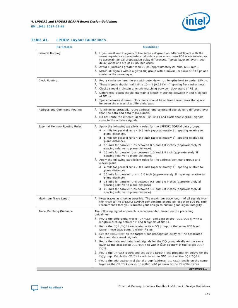
Table 41. LPDD2 Layout Guidelines
Parameter Guidelines
General Routing • If you must route signals of the same net group on different layers with thesame impedance characteristic, simulate your worst case PCB trace tolerancesto ascertain actual propagation delay differences. Typical layer to layer tracedelay variations are of 15 ps/inch order.
• Avoid T-junctions greater than 75 ps (approximately 25 mils, 6.35 mm).• Match all signals within a given DQ group with a maximum skew of ±10 ps and
route on the same layer.
Clock Routing • Route clocks on inner layers with outer-layer run lengths held to under 150 ps.• These signals should maintain a 10-mil (0.254 mm) spacing from other nets.• Clocks should maintain a length-matching between clock pairs of ±5 ps.• Differential clocks should maintain a length-matching between P and N signals
of ±2 ps.• Space between different clock pairs should be at least three times the space
between the traces of a differential pair.
Address and Command Routing • To minimize crosstalk, route address, and command signals on a different layerthan the data and data mask signals.
• Do not route the differential clock (CK/CK#) and clock enable (CKE) signalsclose to the address signals.
External Memory Routing Rules • Apply the following parallelism rules for the LPDDR2 SDRAM data groups:— 4 mils for parallel runs < 0.1 inch (approximately 1× spacing relative to
plane distance).— 5 mils for parallel runs < 0.5 inch (approximately 1× spacing relative to
plane distance).— 10 mils for parallel runs between 0.5 and 1.0 inches (approximately 2×
spacing relative to plane distance).— 15 mils for parallel runs between 1.0 and 2.8 inch (approximately 3×
spacing relative to plane distance).• Apply the following parallelism rules for the address/command group and
clocks group:— 4 mils for parallel runs < 0.1 inch (approximately 1× spacing relative to
plane distance)— 10 mils for parallel runs < 0.5 inch (approximately 2× spacing relative to
plane distance)— 15 mils for parallel runs between 0.5 and 1.0 inches (approximately 3×
spacing relative to plane distance)— 20 mils for parallel runs between 1.0 and 2.8 inches (approximately 4×
spacing relative to plane distance)
Maximum Trace Length • Keep traces as short as possible. The maximum trace length of all signals fromthe FPGA to the LPDDR2 SDRAM components should be less than 509 ps. Intelrecommends that you simulate your design to ensure good signal integrity.
Trace Matching Guidance The following layout approach is recommended, based on the precedingguidelines:1. Route the differential clocks (CK/CK#) and data strobe (DQS/DQS#) with a
length-matching between P and N signals of ±2 ps.2. Route the DQS /DQS# associated with a DQ group on the same PCB layer.
Match these DQS pairs to within ±5 ps.3. Set the DQS/DQS# as the target trace propagation delay for the associated
data and data mask signals.4. Route the data and data mask signals for the DQ group ideally on the same
layer as the associated DQS/DQS# to within ±10 ps skew of the target DQS/DQS#.
5. Route the CK/CK# clocks and set as the target trace propagation delays for theDQ group. Match the CK/CK# clock to within ±50 ps of all the DQS/DQS#.
6. Route the address/control signal group (address, CS, CKE) ideally on the samelayer as the CK/CK# clocks, to within ±20 ps skew of the CK/CK# traces.
continued...
4. LPDDR2 and LPDDR3 SDRAM Board Design Guidelines
EMI_DG | 2017.05.08
Send Feedback External Memory Interface Handbook Volume 2: Design Guidelines
149
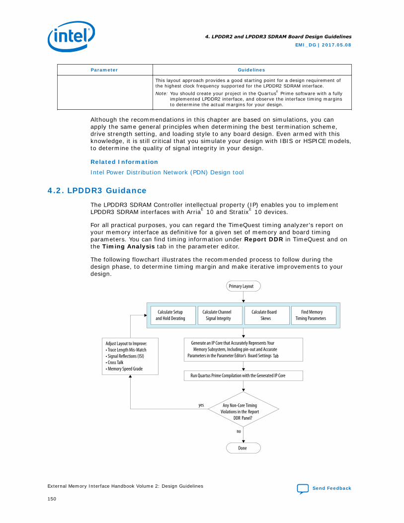
Parameter Guidelines
This layout approach provides a good starting point for a design requirement ofthe highest clock frequency supported for the LPDDR2 SDRAM interface.Note: You should create your project in the Quartus® Prime software with a fully
implemented LPDDR2 interface, and observe the interface timing marginsto determine the actual margins for your design.
Although the recommendations in this chapter are based on simulations, you canapply the same general principles when determining the best termination scheme,drive strength setting, and loading style to any board design. Even armed with thisknowledge, it is still critical that you simulate your design with IBIS or HSPICE models,to determine the quality of signal integrity in your design.
Related Information
Intel Power Distribution Network (PDN) Design tool
4.2. LPDDR3 Guidance
The LPDDR3 SDRAM Controller intellectual property (IP) enables you to implementLPDDR3 SDRAM interfaces with Arria® 10 and Stratix® 10 devices.
For all practical purposes, you can regard the TimeQuest timing analyzer's report onyour memory interface as definitive for a given set of memory and board timingparameters. You can find timing information under Report DDR in TimeQuest and onthe Timing Analysis tab in the parameter editor.
The following flowchart illustrates the recommended process to follow during thedesign phase, to determine timing margin and make iterative improvements to yourdesign.
Primary Layout
Calculate Setupand Hold Derating
Calculate ChannelSignal Integrity
Calculate BoardSkews
Find MemoryTiming Parameters
Generate an IP Core that Accurately Represents Your Memory Subsystem, Including pin-out and Accurate
Parameters in the Parameter Editor’s Board Settings Tab
Run Quartus Prime Compilation with the Generated IP Core
Any Non-Core TimingViolations in the Report
DDR Panel?
yes
no
Done
Adjust Layout to Improve:• Trace Length Mis-Match• Signal Reflections (ISI)• Cross Talk• Memory Speed Grade
4. LPDDR2 and LPDDR3 SDRAM Board Design Guidelines
EMI_DG | 2017.05.08
External Memory Interface Handbook Volume 2: Design Guidelines Send Feedback
150
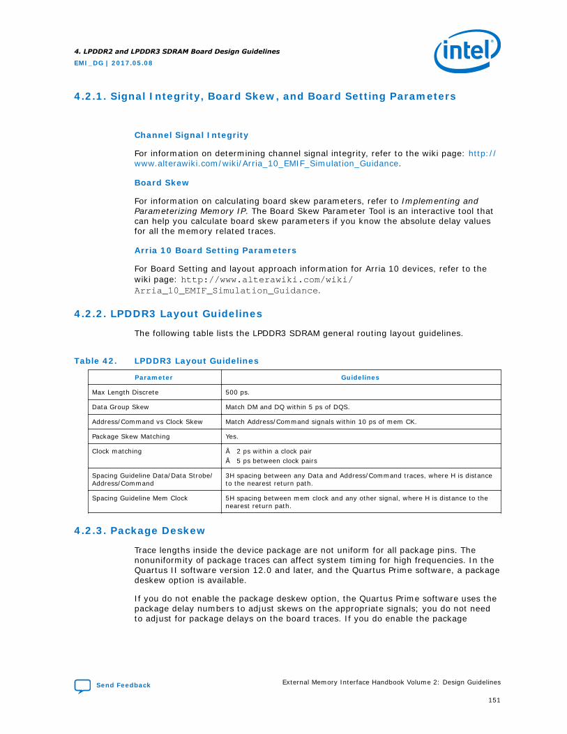
4.2.1. Signal Integrity, Board Skew, and Board Setting Parameters
Channel Signal Integrity
For information on determining channel signal integrity, refer to the wiki page: http://www.alterawiki.com/wiki/Arria_10_EMIF_Simulation_Guidance.
Board Skew
For information on calculating board skew parameters, refer to Implementing andParameterizing Memory IP. The Board Skew Parameter Tool is an interactive tool thatcan help you calculate board skew parameters if you know the absolute delay valuesfor all the memory related traces.
Arria 10 Board Setting Parameters
For Board Setting and layout approach information for Arria 10 devices, refer to thewiki page: http://www.alterawiki.com/wiki/Arria_10_EMIF_Simulation_Guidance.
4.2.2. LPDDR3 Layout Guidelines
The following table lists the LPDDR3 SDRAM general routing layout guidelines.
Table 42. LPDDR3 Layout Guidelines
Parameter Guidelines
Max Length Discrete 500 ps.
Data Group Skew Match DM and DQ within 5 ps of DQS.
Address/Command vs Clock Skew Match Address/Command signals within 10 ps of mem CK.
Package Skew Matching Yes.
Clock matching • 2 ps within a clock pair• 5 ps between clock pairs
Spacing Guideline Data/Data Strobe/Address/Command
3H spacing between any Data and Address/Command traces, where H is distanceto the nearest return path.
Spacing Guideline Mem Clock 5H spacing between mem clock and any other signal, where H is distance to thenearest return path.
4.2.3. Package Deskew
Trace lengths inside the device package are not uniform for all package pins. Thenonuniformity of package traces can affect system timing for high frequencies. In theQuartus II software version 12.0 and later, and the Quartus Prime software, a packagedeskew option is available.
If you do not enable the package deskew option, the Quartus Prime software uses thepackage delay numbers to adjust skews on the appropriate signals; you do not needto adjust for package delays on the board traces. If you do enable the package
4. LPDDR2 and LPDDR3 SDRAM Board Design Guidelines
EMI_DG | 2017.05.08
Send Feedback External Memory Interface Handbook Volume 2: Design Guidelines
151
deskew option, the Quartus Prime software does not use the package delay numbersfor timing analysis, and you must deskew the package delays with the board traces forthe appropriate signals for your design.
4.2.3.1. DQ/DQS/DM Deskew
To get the package delay information, follow these steps:
1. Select the FPGA DQ/DQS Package Skews Deskewed on Board checkbox onthe Board Settings tab of the parameter editor.
2. Generate your IP.
3. Instantiate your IP in the project.
4. Run Analysis and Synthesis in the Quartus Prime software. (Skip this step if youare using an Arria 10 device.)
5. Run the <core_name>_p0_pin_assignment.tcl script. (Skip this step if youare using an Arria 10 device.)
6. Compile your design.
7. Refer to the All Package Pins compilation report, or find the pin delays displayedin the <core_name>.pin file.
4.2.3.2. Address and Command Deskew
Deskew address and command delays as follows:
1. Select the FPGA Address/Command Package Skews Deskewed on Boardcheckbox on the Board Settings tab of the parameter editor.
2. Generate your IP.
3. Instantiate your IP in the project.
4. Run Analysis and Synthesis in the Quartus Prime software. (Skip this step if youare using an Arria 10 device.)
5. Run the <core_name>_p0_pin_assignment.tcl script. (Skip this step if youare using an Arria 10 device.)
6. Compile your design.
7. Refer to the All Package Pins compilation report, or find the pin delays displayedin the <core_name>.pin file.
4.2.3.3. Package Deskew Recommendations for Arria 10 and Stratix 10 Devices
The following table shows package deskew recommendations for all protocolssupported on Arria 10 devices.
As operating frequencies increase, it becomes increasingly critical to perform packagedeskew. The frequencies listed in the table are the minimum frequencies for which youmust perform package deskew.
If you plan to use a listed protocol at the specified frequency or higher, you mustperform package deskew. For example, you must perform package deskew if you planto use dual-rank DDR4 at 800 MHz or above.
4. LPDDR2 and LPDDR3 SDRAM Board Design Guidelines
EMI_DG | 2017.05.08
External Memory Interface Handbook Volume 2: Design Guidelines Send Feedback
152
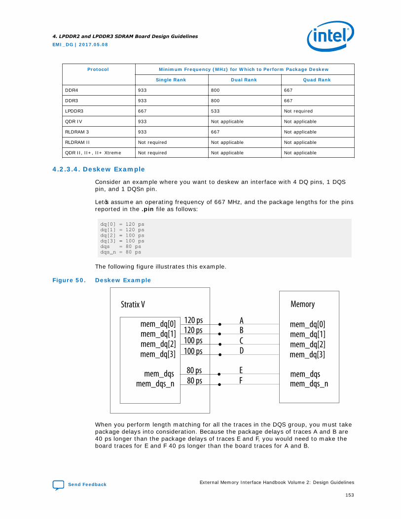
Protocol Minimum Frequency (MHz) for Which to Perform Package Deskew
Single Rank Dual Rank Quad Rank
DDR4 933 800 667
DDR3 933 800 667
LPDDR3 667 533 Not required
QDR IV 933 Not applicable Not applicable
RLDRAM 3 933 667 Not applicable
RLDRAM II Not required Not applicable Not applicable
QDR II, II+, II+ Xtreme Not required Not applicable Not applicable
4.2.3.4. Deskew Example
Consider an example where you want to deskew an interface with 4 DQ pins, 1 DQSpin, and 1 DQSn pin.
Let’s assume an operating frequency of 667 MHz, and the package lengths for the pinsreported in the .pin file as follows:
dq[0] = 120 psdq[1] = 120 psdq[2] = 100 psdq[3] = 100 psdqs = 80 psdqs_n = 80 ps
The following figure illustrates this example.
Figure 50. Deskew Example
Stratix V
mem_dq[0]mem_dq[1]mem_dq[2]mem_dq[3]
mem_dqsmem_dqs_n
mem_dq[0]mem_dq[1]mem_dq[2]mem_dq[3]
mem_dqsmem_dqs_n
Memory
120 ps120 ps100 ps100 ps
80 ps80 ps
ABCD
EF
When you perform length matching for all the traces in the DQS group, you must takepackage delays into consideration. Because the package delays of traces A and B are40 ps longer than the package delays of traces E and F, you would need to make theboard traces for E and F 40 ps longer than the board traces for A and B.
4. LPDDR2 and LPDDR3 SDRAM Board Design Guidelines
EMI_DG | 2017.05.08
Send Feedback External Memory Interface Handbook Volume 2: Design Guidelines
153
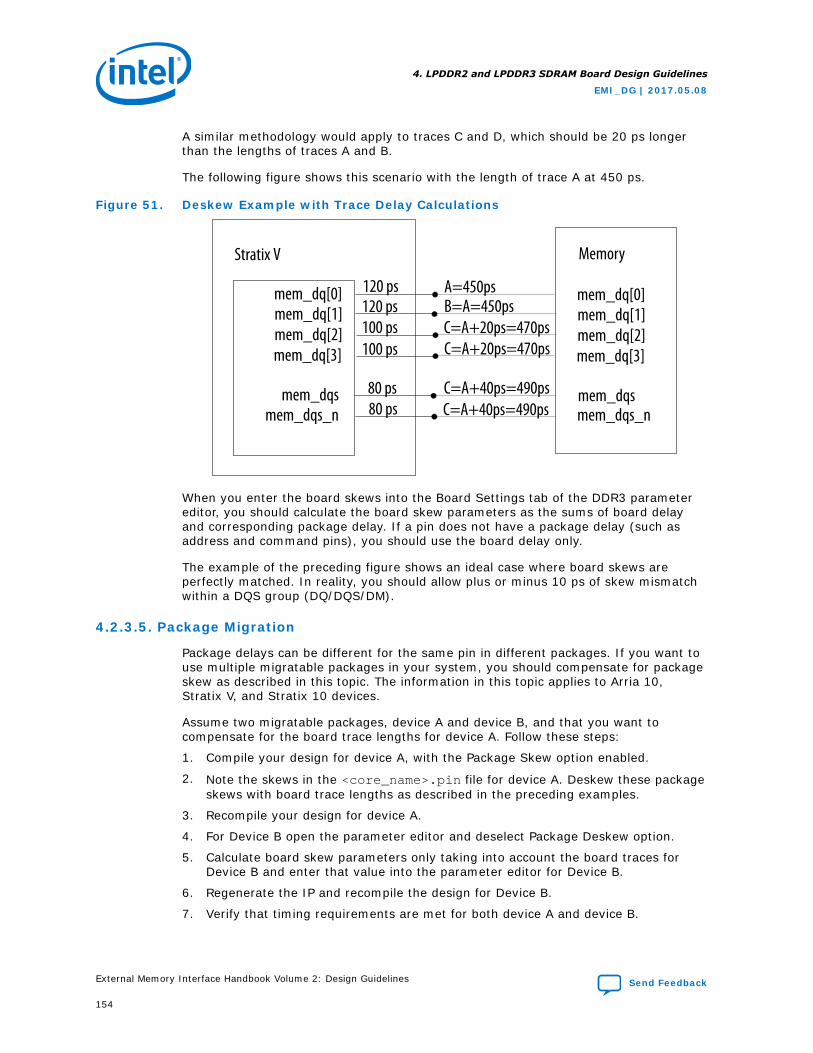
A similar methodology would apply to traces C and D, which should be 20 ps longerthan the lengths of traces A and B.
The following figure shows this scenario with the length of trace A at 450 ps.
Figure 51. Deskew Example with Trace Delay Calculations
Stratix V
mem_dq[0]mem_dq[1]mem_dq[2]mem_dq[3]
mem_dqsmem_dqs_n
mem_dq[0]mem_dq[1]mem_dq[2]mem_dq[3]
mem_dqsmem_dqs_n
Memory
120 ps120 ps100 ps100 ps
80 ps80 ps
A=450psB=A=450psC=A+20ps=470psC=A+20ps=470ps
C=A+40ps=490psC=A+40ps=490ps
When you enter the board skews into the Board Settings tab of the DDR3 parametereditor, you should calculate the board skew parameters as the sums of board delayand corresponding package delay. If a pin does not have a package delay (such asaddress and command pins), you should use the board delay only.
The example of the preceding figure shows an ideal case where board skews areperfectly matched. In reality, you should allow plus or minus 10 ps of skew mismatchwithin a DQS group (DQ/DQS/DM).
4.2.3.5. Package Migration
Package delays can be different for the same pin in different packages. If you want touse multiple migratable packages in your system, you should compensate for packageskew as described in this topic. The information in this topic applies to Arria 10,Stratix V, and Stratix 10 devices.
Assume two migratable packages, device A and device B, and that you want tocompensate for the board trace lengths for device A. Follow these steps:
1. Compile your design for device A, with the Package Skew option enabled.
2. Note the skews in the <core_name>.pin file for device A. Deskew these packageskews with board trace lengths as described in the preceding examples.
3. Recompile your design for device A.
4. For Device B open the parameter editor and deselect Package Deskew option.
5. Calculate board skew parameters only taking into account the board traces forDevice B and enter that value into the parameter editor for Device B.
6. Regenerate the IP and recompile the design for Device B.
7. Verify that timing requirements are met for both device A and device B.
4. LPDDR2 and LPDDR3 SDRAM Board Design Guidelines
EMI_DG | 2017.05.08
External Memory Interface Handbook Volume 2: Design Guidelines Send Feedback
154
4.3. Document Revision History
Date Version Changes
May 2017 2017.5.08 • Added Stratix 10 to Package Deskew and Package Migration sections.• Rebranded as Intel.
October 2016 2016.10.31 Maintenance release.
May 2016 2016.05.02 • Changed recommended value of skew mismatch in Deskew Example topic.
November 2015 2015.11.02 • Changed instances of Quartus II to Quartus Prime.• Added content for LPDDR3.
May 2015 2015.05.04 Maintenance release.
December 2014 2014.12.15 Maintenance release.
August 2014 2014.08.15 • Removed millimeter approximations from lengths expressed inpicoseconds in LPDDR2 Layout Guidelines table.
• Minor formatting fixes in LPDDR2 Layout Guidelines table.
December 2013 2013.12.16 Consolidated General Layout Guidelines.
November 2012 1.0 Initial release.
4. LPDDR2 and LPDDR3 SDRAM Board Design Guidelines
EMI_DG | 2017.05.08
Send Feedback External Memory Interface Handbook Volume 2: Design Guidelines
155
5. RLDRAM II and RLDRAM 3 Board Design GuidelinesThe following topics provide layout guidelines for you to improve your system's signalintegrity and to successfully implement an RLDRAM II or RLDRAM 3 interface.
The RLDRAM II Controller with UniPHY intellectual property (IP) enables you toimplement common I/O (CIO) RLDRAM II interfaces with Arria® V, Stratix® III,Stratix IV, and Stratix V devices. The RLDRAM 3 UniPHY IP enables you to implementCIO RLDRAM 3 interfaces with Stratix V and Arria V GZ devices. You can implementseparate I/O (SIO) RLDRAM II or RLDRAM 3 interfaces with the ALTDQ_DQS orALTDQ_DQS2 IP cores.
The following topics focus on the following key factors that affect signal integrity:
• I/O standards
• RLDRAM II and RLDRAM 3 configurations
• Signal terminations
• Printed circuit board (PCB) layout guidelines
I/O Standards
RLDRAM II interface signals use one of the following JEDEC I/O signalling standards:
• HSTL-15—provides the advantages of lower power and lower emissions.
• HSTL-18—provides increased noise immunity with slightly greater output voltageswings.
RLDRAM 3 interface signals use the following JEDEC I/O signalling standards:HSTL 1.2 V and SSTL-12.
To select the most appropriate standard for your interface, refer to the following:
• Device Data Sheet for Arria II Devices chapter in the Arria II Device Handbook
• Device Data Sheet for Arria V Devices chapter in the Arria V Device Handbook
• Stratix III Device Data Sheet: DC and Switching Characteristics chapter in theStratix III Device Handbook
• DC and Switching Characteristics for Stratix IV Devices chapter in the Stratix IVDevice Handbook
• DC and Switching Characteristics for Stratix V Devices chapter in the Stratix VDevice Handbook
The RLDRAM II Controller with UniPHY IP defaults to HSTL 1.8 V Class I outputs andHSTL 1.8 V inputs. The RLDRAM 3 UniPHY IP defaults to HSTL 1.2 V Class I outputsand HSTL 1.2 V inputs.
Note: The default for RLDRAM 3 changes from Class I to Class II, supporting up to 933 MHz,with the release of the Quartus II software version 12.1 SP1.
EMI_DG | 2017.05.08
Send Feedback
Intel Corporation. All rights reserved. Intel, the Intel logo, Altera, Arria, Cyclone, Enpirion, MAX, Nios, Quartusand Stratix words and logos are trademarks of Intel Corporation or its subsidiaries in the U.S. and/or othercountries. Intel warrants performance of its FPGA and semiconductor products to current specifications inaccordance with Intel's standard warranty, but reserves the right to make changes to any products and servicesat any time without notice. Intel assumes no responsibility or liability arising out of the application or use of anyinformation, product, or service described herein except as expressly agreed to in writing by Intel. Intelcustomers are advised to obtain the latest version of device specifications before relying on any publishedinformation and before placing orders for products or services.*Other names and brands may be claimed as the property of others.
ISO9001:2015Registered
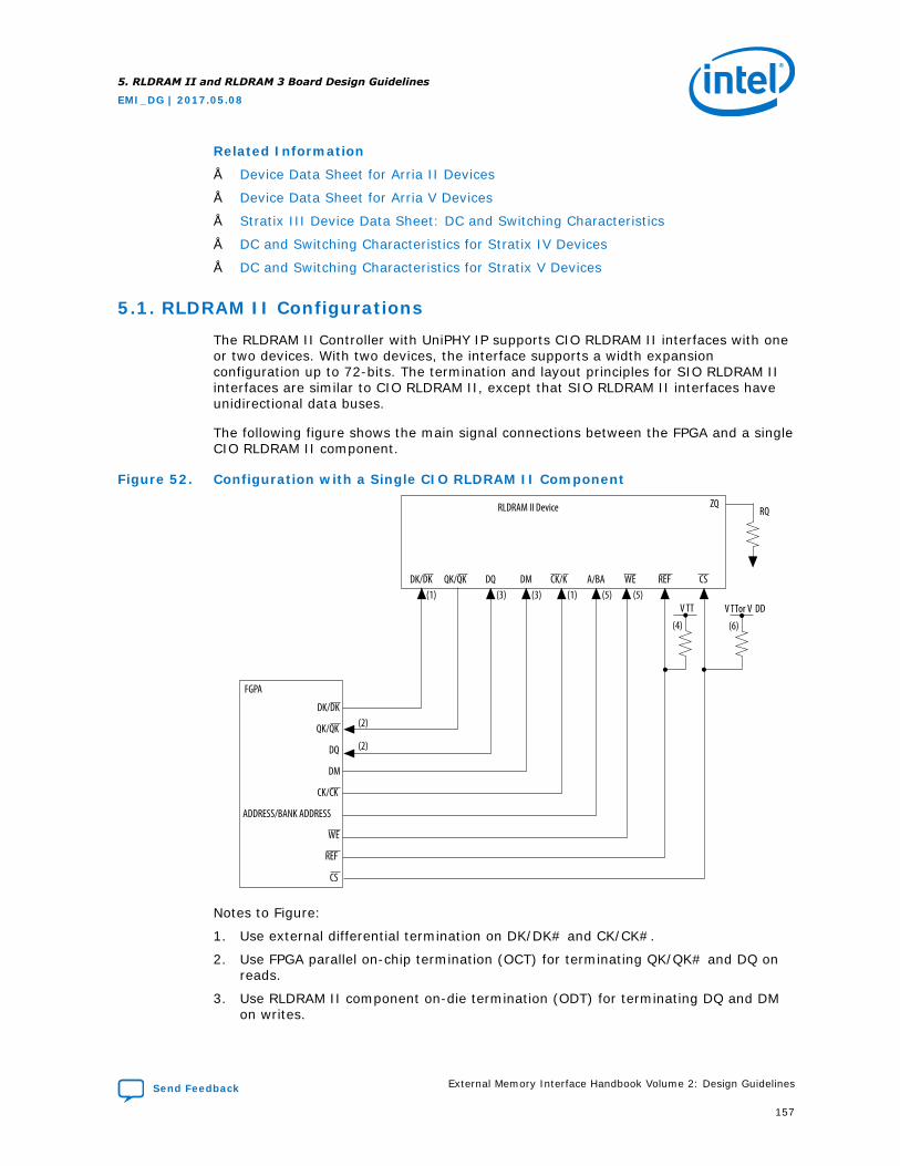
Related Information
• Device Data Sheet for Arria II Devices
• Device Data Sheet for Arria V Devices
• Stratix III Device Data Sheet: DC and Switching Characteristics
• DC and Switching Characteristics for Stratix IV Devices
• DC and Switching Characteristics for Stratix V Devices
5.1. RLDRAM II Configurations
The RLDRAM II Controller with UniPHY IP supports CIO RLDRAM II interfaces with oneor two devices. With two devices, the interface supports a width expansionconfiguration up to 72-bits. The termination and layout principles for SIO RLDRAM IIinterfaces are similar to CIO RLDRAM II, except that SIO RLDRAM II interfaces haveunidirectional data buses.
The following figure shows the main signal connections between the FPGA and a singleCIO RLDRAM II component.
Figure 52. Configuration with a Single CIO RLDRAM II Component
FGPA
RLDRAM II Device ZQRQ
DK/DK DQ DM CK/K A/BA WE REF
QK/QK
DQ
DM
CK/CK
ADDRESS/BANK ADDRESS
WE
REF
CS
QK/QK
DK/DK
CS
(2)
(2)
(3)(1) (3) (1) (5) (5)V TT or V DD
(6)
V TT
(4)
Notes to Figure:
1. Use external differential termination on DK/DK# and CK/CK#.
2. Use FPGA parallel on-chip termination (OCT) for terminating QK/QK# and DQ onreads.
3. Use RLDRAM II component on-die termination (ODT) for terminating DQ and DMon writes.
5. RLDRAM II and RLDRAM 3 Board Design Guidelines
EMI_DG | 2017.05.08
Send Feedback External Memory Interface Handbook Volume 2: Design Guidelines
157
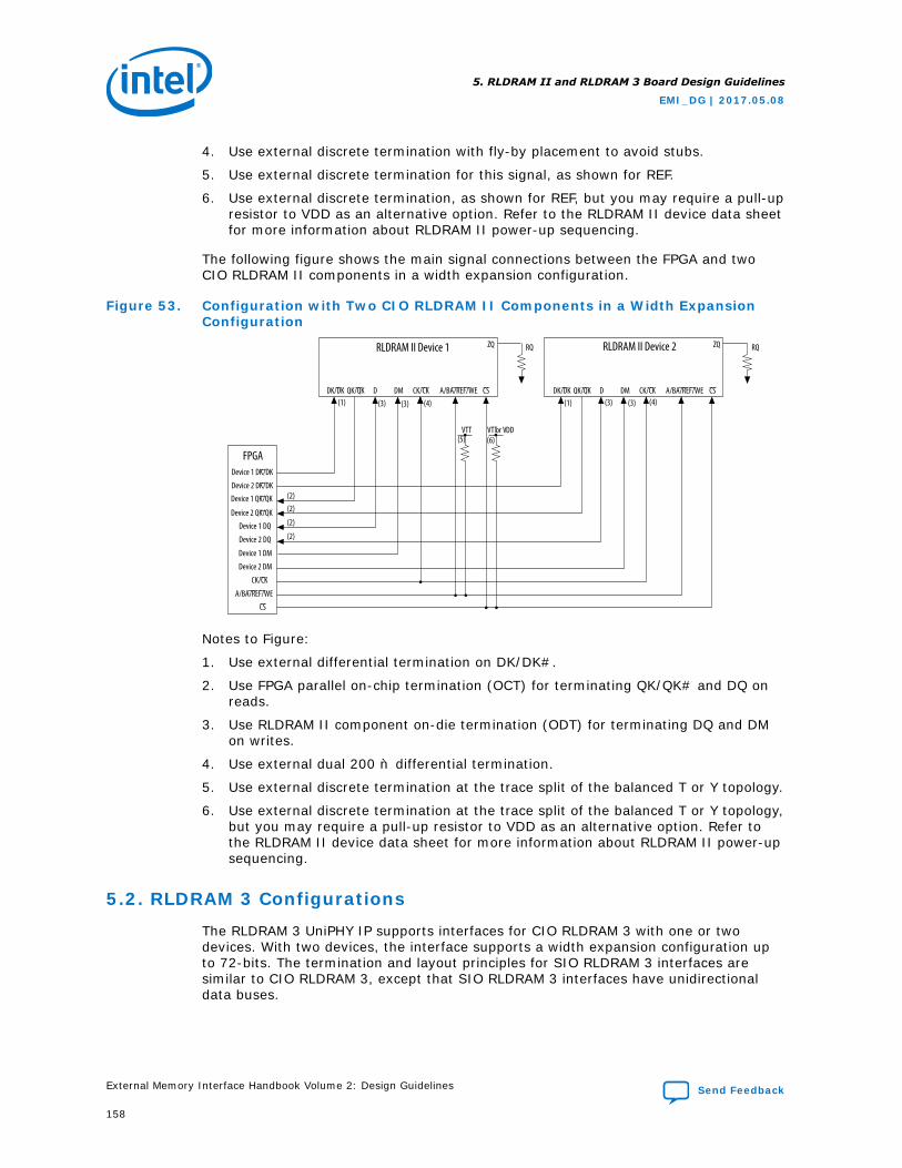
4. Use external discrete termination with fly-by placement to avoid stubs.
5. Use external discrete termination for this signal, as shown for REF.
6. Use external discrete termination, as shown for REF, but you may require a pull-upresistor to VDD as an alternative option. Refer to the RLDRAM II device data sheetfor more information about RLDRAM II power-up sequencing.
The following figure shows the main signal connections between the FPGA and twoCIO RLDRAM II components in a width expansion configuration.
Figure 53. Configuration with Two CIO RLDRAM II Components in a Width ExpansionConfiguration
CK/CK
A/BA/REF/WE
CS
Device 1 QK/QK
Device 2 QK/QK
Device 2 DK/DK(2)(2)
(2)
(2)Device 1 DQ
Device 2 DQ
Device 1 DM
Device 2 DM
RLDRAM II Device 1 ZQ RQ RLDRAM II Device 2 ZQ RQ
(4)(1) (3)
(6)VTT or VDD
(5)VTT
DK/DK QK/QK D DM CK/CK A/BA/REF/WE CS
Device 1 DK/DK
FPGA
DK/DK QK/QK D DM CK/CK A/BA/REF/WE CS
(3) (1) (3)(3) (4)
Notes to Figure:
1. Use external differential termination on DK/DK#.
2. Use FPGA parallel on-chip termination (OCT) for terminating QK/QK# and DQ onreads.
3. Use RLDRAM II component on-die termination (ODT) for terminating DQ and DMon writes.
4. Use external dual 200 Ω differential termination.
5. Use external discrete termination at the trace split of the balanced T or Y topology.
6. Use external discrete termination at the trace split of the balanced T or Y topology,but you may require a pull-up resistor to VDD as an alternative option. Refer tothe RLDRAM II device data sheet for more information about RLDRAM II power-upsequencing.
5.2. RLDRAM 3 Configurations
The RLDRAM 3 UniPHY IP supports interfaces for CIO RLDRAM 3 with one or twodevices. With two devices, the interface supports a width expansion configuration upto 72-bits. The termination and layout principles for SIO RLDRAM 3 interfaces aresimilar to CIO RLDRAM 3, except that SIO RLDRAM 3 interfaces have unidirectionaldata buses.
5. RLDRAM II and RLDRAM 3 Board Design Guidelines
EMI_DG | 2017.05.08
External Memory Interface Handbook Volume 2: Design Guidelines Send Feedback
158
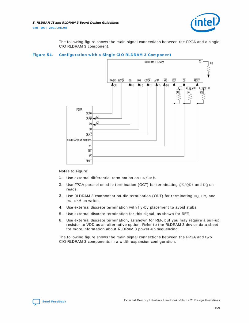
The following figure shows the main signal connections between the FPGA and a singleCIO RLDRAM 3 component.
Figure 54. Configuration with a Single CIO RLDRAM 3 Component
FGPA
RLDRAM 3 Device ZQ RQ
DK/DK DQ DM CK/CK A/BA WE REF
QK/QK
DQ
DM
CK/CK
ADDRESS/BANK ADDRESS
WE
REF
CS
QK/QK
DK/DK
CS RESET
(2)
(2)
(3)(3) (3) (1) (5) (5)VTT or V DD
(6)VTT or V DD
(6)VTT
(4)
RESET
Notes to Figure:
1. Use external differential termination on CK/CK#.
2. Use FPGA parallel on-chip termination (OCT) for terminating QK/QK# and DQ onreads.
3. Use RLDRAM 3 component on-die termination (ODT) for terminating DQ, DM, andDK, DK# on writes.
4. Use external discrete termination with fly-by placement to avoid stubs.
5. Use external discrete termination for this signal, as shown for REF.
6. Use external discrete termination, as shown for REF, but you may require a pull-upresistor to VDD as an alternative option. Refer to the RLDRAM 3 device data sheetfor more information about RLDRAM 3 power-up sequencing.
The following figure shows the main signal connections between the FPGA and twoCIO RLDRAM 3 components in a width expansion configuration.
5. RLDRAM II and RLDRAM 3 Board Design Guidelines
EMI_DG | 2017.05.08
Send Feedback External Memory Interface Handbook Volume 2: Design Guidelines
159
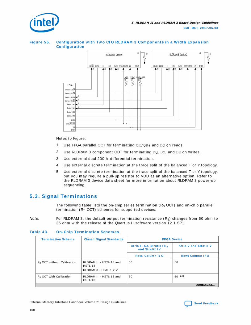
Figure 55. Configuration with Two CIO RLDRAM 3 Components in a Width ExpansionConfiguration
CK/CK
A/BA/REF/WE
CS
Device 1 QK/QK
Device 2 QK/QK
Device 2 DK/DK(1)
(1)
(1)
(1)Device 1 DQ
Device 2 DQ
Device 1 DM
Device 2 DM
RLDRAM 3 Device 1ZQ RQ RLDRAM 3 Device 2
ZQ RQ
(3)(2)
(5)V TT or V DD
(5)V TT or V DD
(4)V TT
DK/DK QK/QK D DM CK/CK A/BA/REF/WE CS
Device 1 DK/DK
FPGA
DK/DK QK/QK D DM CS RESET
RESET
RESETCK/CK A/BA/REF/WE(2) (2)(2) (3)(3) (3)
Notes to Figure:
1. Use FPGA parallel OCT for terminating QK/QK# and DQ on reads.
2. Use RLDRAM 3 component ODT for terminating DQ, DM, and DK on writes.
3. Use external dual 200 Ω differential termination.
4. Use external discrete termination at the trace split of the balanced T or Y topology.
5. Use external discrete termination at the trace split of the balanced T or Y topology,but you may require a pull-up resistor to VDD as an alternative option. Refer tothe RLDRAM 3 device data sheet for more information about RLDRAM 3 power-upsequencing.
5.3. Signal Terminations
The following table lists the on-chip series termination (RS OCT) and on-chip paralleltermination (RT OCT) schemes for supported devices.
Note: For RLDRAM 3, the default output termination resistance (RS) changes from 50 ohm to25 ohm with the release of the Quartus II software version 12.1 SP1.
Table 43. On-Chip Termination Schemes
Termination Scheme Class I Signal Standards FPGA Device
Arria II GZ, Stratix III,and Stratix IV
Arria V and Stratix V
Row/Column I/O Row/Column I/O
RS OCT without Calibration RLDRAM II - HSTL-15 andHSTL-18RLDRAM 3 - HSTL 1.2 V
50 50
RS OCT with Calibration RLDRAM II - HSTL-15 andHSTL-18
50 50 (1)
continued...
5. RLDRAM II and RLDRAM 3 Board Design Guidelines
EMI_DG | 2017.05.08
External Memory Interface Handbook Volume 2: Design Guidelines Send Feedback
160
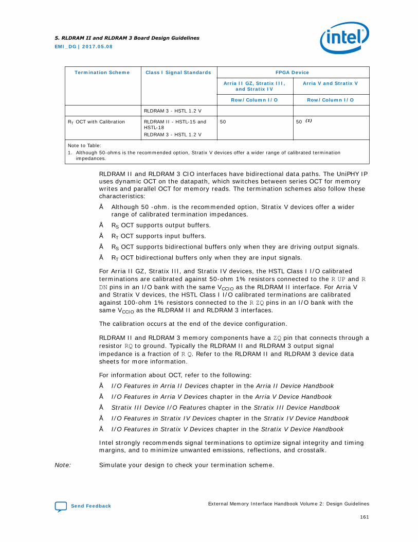
Termination Scheme Class I Signal Standards FPGA Device
Arria II GZ, Stratix III,and Stratix IV
Arria V and Stratix V
Row/Column I/O Row/Column I/O
RLDRAM 3 - HSTL 1.2 V
RT OCT with Calibration RLDRAM II - HSTL-15 andHSTL-18RLDRAM 3 - HSTL 1.2 V
50 50 (1)
Note to Table:1. Although 50-ohms is the recommended option, Stratix V devices offer a wider range of calibrated termination
impedances.
RLDRAM II and RLDRAM 3 CIO interfaces have bidirectional data paths. The UniPHY IPuses dynamic OCT on the datapath, which switches between series OCT for memorywrites and parallel OCT for memory reads. The termination schemes also follow thesecharacteristics:
• Although 50 -ohm. is the recommended option, Stratix V devices offer a widerrange of calibrated termination impedances.
• RS OCT supports output buffers.
• RT OCT supports input buffers.
• RS OCT supports bidirectional buffers only when they are driving output signals.
• RT OCT bidirectional buffers only when they are input signals.
For Arria II GZ, Stratix III, and Stratix IV devices, the HSTL Class I I/O calibratedterminations are calibrated against 50-ohm 1% resistors connected to the R UP and RDN pins in an I/O bank with the same VCCIO as the RLDRAM II interface. For Arria Vand Stratix V devices, the HSTL Class I I/O calibrated terminations are calibratedagainst 100-ohm 1% resistors connected to the R ZQ pins in an I/O bank with thesame VCCIO as the RLDRAM II and RLDRAM 3 interfaces.
The calibration occurs at the end of the device configuration.
RLDRAM II and RLDRAM 3 memory components have a ZQ pin that connects through aresistor RQ to ground. Typically the RLDRAM II and RLDRAM 3 output signalimpedance is a fraction of R Q. Refer to the RLDRAM II and RLDRAM 3 device datasheets for more information.
For information about OCT, refer to the following:
• I/O Features in Arria II Devices chapter in the Arria II Device Handbook
• I/O Features in Arria V Devices chapter in the Arria V Device Handbook
• Stratix III Device I/O Features chapter in the Stratix III Device Handbook
• I/O Features in Stratix IV Devices chapter in the Stratix IV Device Handbook
• I/O Features in Stratix V Devices chapter in the Stratix V Device Handbook
Intel strongly recommends signal terminations to optimize signal integrity and timingmargins, and to minimize unwanted emissions, reflections, and crosstalk.
Note: Simulate your design to check your termination scheme.
5. RLDRAM II and RLDRAM 3 Board Design Guidelines
EMI_DG | 2017.05.08
Send Feedback External Memory Interface Handbook Volume 2: Design Guidelines
161
Related Information
• I/O Features in Arria II Devices
• I/O Features in Arria V Devices
• Stratix III Device I/O Features
• I/O Features in Stratix IV Devices
• I/O Features in Stratix V Devices
5.3.1. Input to the FPGA from the RLDRAM Components
The RLDRAM II or RLDRAM 3 component drives the following input signals into theFPGA:
• Read data (DQ on the bidirectional data signals for CIO RLDRAM II and CIORLDRAM 3).
• Read clocks (QK/QK#).
Intel recommends that you use the FPGA parallel OCT to terminate the data on readsand read clocks.
5.3.2. Outputs from the FPGA to the RLDRAM II and RLDRAM 3Components
The following output signals are from the FPGA to the RLDRAM II and RLDRAM 3components:
• Write data (DQ on the bidirectional data signals for CIO RLDRAM II and RLDRAM 3)
• Data mask (DM)
• Address, bank address
• Command (CS, WE, and REF)
• Clocks (CK/CK# and DK/DK#)
For point-to-point single-ended signals requiring external termination, Intelrecommends that you place a fly-by termination by terminating at the end of thetransmission line after the receiver to avoid unterminated stubs. The guideline is toplace the fly-by termination within 100 ps propagation delay of the receiver.
Although not recommended, you can place the termination before the receiver, whichleaves an unterminated stub. The stub delay is critical because the stub between thetermination and the receiver is effectively unterminated, causing additional ringingand reflections. Stub delays should be less than 50 ps.
Intel recommends that the differential clocks, CK, CK# and DK, DK# (RLDRAM II) andCK, CK# (RLDRAM 3), use a differential termination at the end of the trace at theexternal memory component. Alternatively, you can terminate each clock output witha parallel termination to VTT.
5. RLDRAM II and RLDRAM 3 Board Design Guidelines
EMI_DG | 2017.05.08
External Memory Interface Handbook Volume 2: Design Guidelines Send Feedback
162
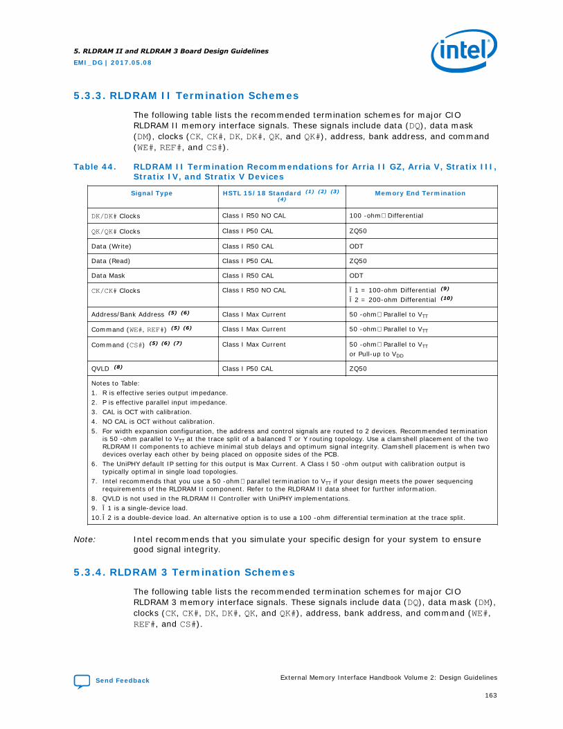
5.3.3. RLDRAM II Termination Schemes
The following table lists the recommended termination schemes for major CIORLDRAM II memory interface signals. These signals include data (DQ), data mask(DM), clocks (CK, CK#, DK, DK#, QK, and QK#), address, bank address, and command(WE#, REF#, and CS#).
Table 44. RLDRAM II Termination Recommendations for Arria II GZ, Arria V, Stratix III,Stratix IV, and Stratix V Devices
Signal Type HSTL 15/18 Standard (1) (2) (3) (4)
Memory End Termination
DK/DK# Clocks Class I R50 NO CAL 100 -ohmDifferential
QK/QK# Clocks Class I P50 CAL ZQ50
Data (Write) Class I R50 CAL ODT
Data (Read) Class I P50 CAL ZQ50
Data Mask Class I R50 CAL ODT
CK/CK# Clocks Class I R50 NO CAL ×1 = 100-ohm Differential (9)
×2 = 200-ohm Differential (10)
Address/Bank Address (5) (6) Class I Max Current 50 -ohmParallel to VTT
Command (WE#, REF#) (5) (6) Class I Max Current 50 -ohmParallel to VTT
Command (CS#) (5) (6) (7) Class I Max Current 50 -ohmParallel to VTT
or Pull-up to VDD
QVLD (8) Class I P50 CAL ZQ50
Notes to Table:1. R is effective series output impedance.2. P is effective parallel input impedance.3. CAL is OCT with calibration.4. NO CAL is OCT without calibration.5. For width expansion configuration, the address and control signals are routed to 2 devices. Recommended termination
is 50 -ohm parallel to VTT at the trace split of a balanced T or Y routing topology. Use a clamshell placement of the twoRLDRAM II components to achieve minimal stub delays and optimum signal integrity. Clamshell placement is when twodevices overlay each other by being placed on opposite sides of the PCB.
6. The UniPHY default IP setting for this output is Max Current. A Class I 50 -ohm output with calibration output istypically optimal in single load topologies.
7. Intel recommends that you use a 50 -ohmparallel termination to VTT if your design meets the power sequencingrequirements of the RLDRAM II component. Refer to the RLDRAM II data sheet for further information.
8. QVLD is not used in the RLDRAM II Controller with UniPHY implementations.9. ×1 is a single-device load.10.×2 is a double-device load. An alternative option is to use a 100 -ohm differential termination at the trace split.
Note: Intel recommends that you simulate your specific design for your system to ensuregood signal integrity.
5.3.4. RLDRAM 3 Termination Schemes
The following table lists the recommended termination schemes for major CIORLDRAM 3 memory interface signals. These signals include data (DQ), data mask (DM),clocks (CK, CK#, DK, DK#, QK, and QK#), address, bank address, and command (WE#,REF#, and CS#).
5. RLDRAM II and RLDRAM 3 Board Design Guidelines
EMI_DG | 2017.05.08
Send Feedback External Memory Interface Handbook Volume 2: Design Guidelines
163
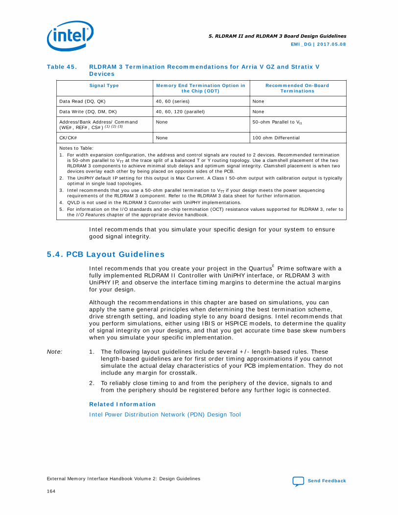
Table 45. RLDRAM 3 Termination Recommendations for Arria V GZ and Stratix VDevices
Signal Type Memory End Termination Option inthe Chip (ODT)
Recommended On-BoardTerminations
Data Read (DQ, QK) 40, 60 (series) None
Data Write (DQ, DM, DK) 40, 60, 120 (parallel) None
Address/Bank Address/ Command(WE#, REF#, CS#) (1) (2) (3)
None 50-ohm Parallel to Vtt
CK/CK# None 100 ohm Differential
Notes to Table:1. For width expansion configuration, the address and control signals are routed to 2 devices. Recommended termination
is 50-ohm parallel to VTT at the trace split of a balanced T or Y routing topology. Use a clamshell placement of the twoRLDRAM 3 components to achieve minimal stub delays and optimum signal integrity. Clamshell placement is when twodevices overlay each other by being placed on opposite sides of the PCB.
2. The UniPHY default IP setting for this output is Max Current. A Class I 50-ohm output with calibration output is typicallyoptimal in single load topologies.
3. Intel recommends that you use a 50-ohm parallel termination to VTT if your design meets the power sequencingrequirements of the RLDRAM 3 component. Refer to the RLDRAM 3 data sheet for further information.
4. QVLD is not used in the RLDRAM 3 Controller with UniPHY implementations.5. For information on the I/O standards and on-chip termination (OCT) resistance values supported for RLDRAM 3, refer to
the I/O Features chapter of the appropriate device handbook.
Intel recommends that you simulate your specific design for your system to ensuregood signal integrity.
5.4. PCB Layout Guidelines
Intel recommends that you create your project in the Quartus® Prime software with afully implemented RLDRAM II Controller with UniPHY interface, or RLDRAM 3 withUniPHY IP, and observe the interface timing margins to determine the actual marginsfor your design.
Although the recommendations in this chapter are based on simulations, you canapply the same general principles when determining the best termination scheme,drive strength setting, and loading style to any board designs. Intel recommends thatyou perform simulations, either using IBIS or HSPICE models, to determine the qualityof signal integrity on your designs, and that you get accurate time base skew numberswhen you simulate your specific implementation.
Note: 1. The following layout guidelines include several +/- length-based rules. Theselength-based guidelines are for first order timing approximations if you cannotsimulate the actual delay characteristics of your PCB implementation. They do notinclude any margin for crosstalk.
2. To reliably close timing to and from the periphery of the device, signals to andfrom the periphery should be registered before any further logic is connected.
Related Information
Intel Power Distribution Network (PDN) Design Tool
5. RLDRAM II and RLDRAM 3 Board Design Guidelines
EMI_DG | 2017.05.08
External Memory Interface Handbook Volume 2: Design Guidelines Send Feedback
164
5.5. General Layout Guidelines
The following table lists general board design layout guidelines. These guidelines areIntel recommendations, and should not be considered as hard requirements. Youshould perform signal integrity simulation on all the traces to verify the signal integrityof the interface. You should extract the slew rate and propagation delay information,enter it into the IP and compile the design to ensure that timing requirements aremet.
Table 46. General Layout Guidelines
Parameter Guidelines
Impedance • All unused via pads must be removed, because they cause unwantedcapacitance.
• Trace impedance plays an important role in the signal integrity. You mustperform board level simulation to determine the best characteristic impedancefor your PCB. For example, it is possible that for multi rank systems 40 ohmscould yield better results than a traditional 50 ohm characteristic impedance.
Decoupling Parameter • Use 0.1 uF in 0402 size to minimize inductance• Make VTT voltage decoupling close to termination resistors• Connect decoupling caps between VTT and ground• Use a 0.1 uF cap for every other VTT pin and 0.01 uF cap for every VDD and
VDDQ pin• Verify the capacitive decoupling using the Intel Power Distribution Network
Design Tool
Power • Route GND and VCC as planes• Route VCCIO for memories in a single split plane with at least a 20-mil
(0.020 inches, or 0.508 mm) gap of separation• Route VTT as islands or 250-mil (6.35-mm) power traces• Route oscillators and PLL power as islands or 100-mil (2.54-mm) power traces
General Routing All specified delay matching requirements include PCB trace delays, different layerpropagation velocity variance, and crosstalk. To minimize PCB layer propogationvariance, Intel recommends that signals from the same net group always berouted on the same layer.• Use 45° angles (not 90° corners)• Avoid T-Junctions for critical nets or clocks• Avoid T-junctions greater than 250 mils (6.35 mm)• Disallow signals across split planes• Restrict routing other signals close to system reset signals• Avoid routing memory signals closer than 0.025 inch (0.635 mm) to PCI or
system clocks
Related Information
Power Distribution Network Design Tool
5.6. RLDRAM II and RLDRAM 3 Layout Guidelines
The following table lists the RLDRAM II and RLDRAM 3 general routing layoutguidelines. These guidelines apply to Arria V, Arria 10, Stratix V, and Stratix 10devices.
5. RLDRAM II and RLDRAM 3 Board Design Guidelines
EMI_DG | 2017.05.08
Send Feedback External Memory Interface Handbook Volume 2: Design Guidelines
165
Table 47. RLDRAM II and RLDRAM 3 Layout Guidelines
Parameter Guidelines
General Routing • If you must route signals of the same net group on different layers with thesame impedance characteristic, simulate your worst case PCB trace tolerancesto ascertain actual propagation delay differences. Typical layer to layer tracedelay variations are of 15 ps/inch order.
• Avoid T-junctions greater than 150 ps.• Match all signals within a given DQ group with a maximum skew of ±10 ps and
route on the same layer.
Clock Routing • Route clocks on inner layers with outer-layer run lengths held to under 150 ps.• These signals should maintain a 10-mil (0.254 mm) spacing from other nets.• Clocks should maintain a length-matching between clock pairs of ±5 ps.• Differential clocks should maintain a length-matching between P and N signals
of ±2 ps.• Space between different clock pairs should be at least three times the space
between the traces of a differential pair.
Address and Command Routing • To minimize crosstalk, route address, bank address, and command signals on adifferent layer than the data and data mask signals.
• Do not route the differential clock signals close to the address signals.• Keep the distance from the pin on the RLDRAM II or RLDRAM 3 component to
the stub termination resistor (VTT) to less than 50 ps for the address/commandsignal group.
• Keep the distance from the pin on the RLDRAM II or RLDRAM 3 component tothe fly-by termination resistor (VTT) to less than 100 ps for the address/command signal group.
External Memory Routing Rules • Apply the following parallelism rules for the RLDRAM II or RLDRAM 3 data/address/command groups:— 4 mils for parallel runs < 0.1 inch (approximately 1× spacing relative to
plane distance).— 5 mils for parallel runs < 0.5 inch (approximately 1× spacing relative to
plane distance).— 10 mils for parallel runs between 0.5 and 1.0 inches (approximately 2×
spacing relative to plane distance).— 15 mils for parallel runs between 1.0 and 3.3 inch (approximately 3×
spacing relative to plane distance).
Maximum Trace Length • Keep the maximum trace length of all signals from the FPGA to the RLDRAM IIor RLDRAM 3 components to 600 ps.
Trace Matching Guidance The following layout approach is recommended, based on the precedingguidelines:1. If the RLDRAM II interface has multiple DQ groups (×18 or ×36 RLDRAM II/
RLDRAM 3 component or width expansion configuration), match all theDK/DK# and QK ,QK # clocks as tightly as possible to optimize the timingmargins in your design.
2. Route the DK/DK# write clock and QK/QK# read clock associated with a DQgroup on the same PCB layer. Match these clock pairs to within ±5 ps.
3. Set the DK/DK# or QK/QK# clock as the target trace propagation delay for theassociated data and data mask signals.
4. Route the data and data mask signals for the DQ group ideally on the samelayer as the associated QK/QK# and DK/DK# clocks to within ±10 ps skew ofthe target clock.
5. Route the CK/CK# clocks and set as the target trace propagation delays for theaddress/command signal group. Match the CK/CK# clock to within ±50 ps ofall the DK/DK# clocks.
6. Route the address/control signal group (address, bank address, CS, WE, andREF) ideally on the same layer as the CK/CK# clocks, to within ±20 ps skew ofthe CK/CK# traces.
continued...
5. RLDRAM II and RLDRAM 3 Board Design Guidelines
EMI_DG | 2017.05.08
External Memory Interface Handbook Volume 2: Design Guidelines Send Feedback
166
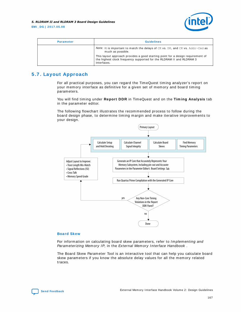
Parameter Guidelines
Note: It is important to match the delays of CK vs. DK, and CK vs. Addr-Cmd asmuch as possible.
This layout approach provides a good starting point for a design requirement ofthe highest clock frequency supported for the RLDRAM II and RLDRAM 3interfaces.
5.7. Layout Approach
For all practical purposes, you can regard the TimeQuest timing analyzer's report onyour memory interface as definitive for a given set of memory and board timingparameters.
You will find timing under Report DDR in TimeQuest and on the Timing Analysis tabin the parameter editor.
The following flowchart illustrates the recommended process to follow during theboard design phase, to determine timing margin and make iterative improvements toyour design.
Primary Layout
Calculate Setupand Hold Derating
Calculate ChannelSignal Integrity
Calculate BoardSkews
Find MemoryTiming Parameters
Generate an IP Core that Accurately Represents Your Memory Subsystem, Including pin-out and Accurate
Parameters in the Parameter Editor’s Board Settings Tab
Run Quartus Prime Compilation with the Generated IP Core
Any Non-Core TimingViolations in the Report
DDR Panel?
yes
no
Done
Adjust Layout to Improve:• Trace Length Mis-Match• Signal Reflections (ISI)• Cross Talk• Memory Speed Grade
Board Skew
For information on calculating board skew parameters, refer to Implementing andParameterizing Memory IP, in the External Memory Interface Handbook .
The Board Skew Parameter Tool is an interactive tool that can help you calculate boardskew parameters if you know the absolute delay values for all the memory relatedtraces.
5. RLDRAM II and RLDRAM 3 Board Design Guidelines
EMI_DG | 2017.05.08
Send Feedback External Memory Interface Handbook Volume 2: Design Guidelines
167

Memory Timing Parameters
For information on the memory timing parameters to be entered into the parametereditor, refer to the datasheet for your external memory device.
Related Information
Board Skew Parameter Tool
5.7.1. Arria V and Stratix V Board Setting Parameters
The following guidelines apply to the Board Setting parameters for Arria V and StratixV devices.
Setup and Hold Derating
For information on calculating derating parameters, refer to Implementing andParameterizing Memory IP, in the External Memory Interface Handbook.
Channel Signal Integrity
For information on determining channel signal integrity for Stratix V and earlierproducts, refer to the wiki page: http://www.alterawiki.com/wiki/Measuring_Channel_Signal_Integrity .
Board Skew
For information on calculating board skew parameters, refer to Implementing andParameterizing Memory IP, in the External Memory Interface Handbook.
The Board Skew Parameter Tool is an interactive tool that can help you calculate boardskew parameters if you know the absolute delay values for all the memory relatedtraces.
Memory Timing Parameters
For information on the memory timing parameters to be entered into the parametereditor, refer to the datasheet for your external memory device.
5.7.2. Arria 10 Board Setting Parameters
For Board Setting and layout approach information for Arria 10 devices, refer to thewiki at the address below.
Arria 10 Board Setting and layout approach information: http://www.alterawiki.com/wiki/Arria_10_EMIF_Simulation_Guidance .
5.8. Package Deskew for RLDRAM II and RLDRAM 3
You should follow Intel's package deskew guidance if you are using Arria 10, Stratix10, or Stratix V devices.
For more information on package deskew, refer to Package Deskew.
Related Information
Package Deskew
5. RLDRAM II and RLDRAM 3 Board Design Guidelines
EMI_DG | 2017.05.08
External Memory Interface Handbook Volume 2: Design Guidelines Send Feedback
168
5.9. Document Revision History
Date Version Changes
May 2017 2017.5.08 • Added Stratix 10 to RLDRAM II and RLDRAM 3 Layout Guidelines section.• Rebranded as Intel.
October 2016 2016.10.31 Maintenance release.
May 2016 2016.05.02 Maintenance release.
November 2015 2015.11.02 • Changed instances of Quartus II to Quartus Prime.
May 2015 2015.05.04 Maintenance release.
December 2014 2014.12.15 Maintenance release.
August 2014 2014.08.15 • Revised RLDRAM 3 Termination Recommendations for Arria V GZ andStratix V Devices table.
• Removed millimeter approximations from lengths expressed inpicoseconds in RLDRAM II and RLDRAM 3 Layout Guidelines table.
• Minor formatting fixes in RLDRAM II and RLDRAM 3 Layout Guidelinestable.
• Added Layout Approach section.
December 2013 2013.12.16 • Added note about byteenable support to Signal Descriptions section.• Consolidated General Layout Guidelines.
November 2012 3.2 Added content supporting RLDRAM 3 and updated RLDRAM II standards.
June 2012 3.1 Added Feedback icon.
November 2011 3.0 Added Arria V information.
June 2011 2.0 Added Stratix V information.
December 2010 1.0 Initial release.
5. RLDRAM II and RLDRAM 3 Board Design Guidelines
EMI_DG | 2017.05.08
Send Feedback External Memory Interface Handbook Volume 2: Design Guidelines
169
6. QDR II and QDR-IV SRAM Board Design GuidelinesThe following topics provide guidelines for you to improve your system's signalintegrity and layout guidelines to help successfully implement a QDR II or QDR II+SRAM interface in your system.
The QDR II and QDR II+ SRAM Controller with UniPHY intellectual property (IP)enables you to implement QDR II and QDR II+ interfaces with Arria® II GX, Arria V,Stratix® III, Stratix IV, and Stratix V devices.
Note: In the following topics, QDR II SRAM refers to both QDR II and QDR II+ SRAM unlessstated otherwise.
The following topics focus on the following key factors that affect signal integrity:
• I/O standards
• QDR II SRAM configurations
• Signal terminations
• Printed circuit board (PCB) layout guidelines
I/O Standards
QDR II SRAM interface signals use one of the following JEDEC I/O signallingstandards:
• HSTL-15—provides the advantages of lower power and lower emissions.
• HSTL-18—provides increased noise immunity with slightly greater output voltageswings.
To select the most appropriate standard for your interface, refer to the Arria II GXDevices Data Sheet: Electrical Characteristics chapter in the Arria II Device Handbook,Stratix III Device Datasheet: DC and Switching Characteristics chapter in the StratixIII Device Handbook, or the Stratix IV Device Datasheet DC and SwitchingCharacteristics chapter in the Stratix IV Device Handbook.
Altera QDR II SRAM Controller with UniPHY IP defaults to HSTL 1.5 V Class I outputsand HSTL 1.5 V inputs.
Related Information
• Arria II GX Devices Data Sheet: Electrical Characteristics
• Stratix III Device Datasheet: DC and Switching Characteristics
• Stratix IV Device Datasheet DC and Switching Characteristics
EMI_DG | 2017.05.08
Send Feedback
Intel Corporation. All rights reserved. Intel, the Intel logo, Altera, Arria, Cyclone, Enpirion, MAX, Nios, Quartusand Stratix words and logos are trademarks of Intel Corporation or its subsidiaries in the U.S. and/or othercountries. Intel warrants performance of its FPGA and semiconductor products to current specifications inaccordance with Intel's standard warranty, but reserves the right to make changes to any products and servicesat any time without notice. Intel assumes no responsibility or liability arising out of the application or use of anyinformation, product, or service described herein except as expressly agreed to in writing by Intel. Intelcustomers are advised to obtain the latest version of device specifications before relying on any publishedinformation and before placing orders for products or services.*Other names and brands may be claimed as the property of others.
ISO9001:2015Registered
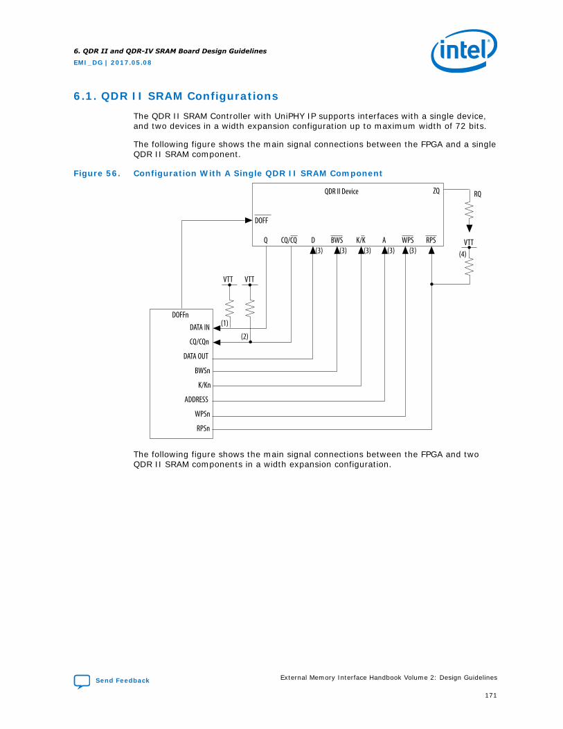
6.1. QDR II SRAM Configurations
The QDR II SRAM Controller with UniPHY IP supports interfaces with a single device,and two devices in a width expansion configuration up to maximum width of 72 bits.
The following figure shows the main signal connections between the FPGA and a singleQDR II SRAM component.
Figure 56. Configuration With A Single QDR II SRAM Component
DOFFn
QDR II Device
DOFF
ZQ RQ
VTT VTT
DATA IN
Q CQ/CQ D BWS K/K A WPS RPS
CQ/CQn
DATA OUT
BWSn
K/Kn
ADDRESS
WPSn
RPSn
VTT
(1)
(2)
(3) (3) (3) (3) (3) (4)
The following figure shows the main signal connections between the FPGA and twoQDR II SRAM components in a width expansion configuration.
6. QDR II and QDR-IV SRAM Board Design Guidelines
EMI_DG | 2017.05.08
Send Feedback External Memory Interface Handbook Volume 2: Design Guidelines
171
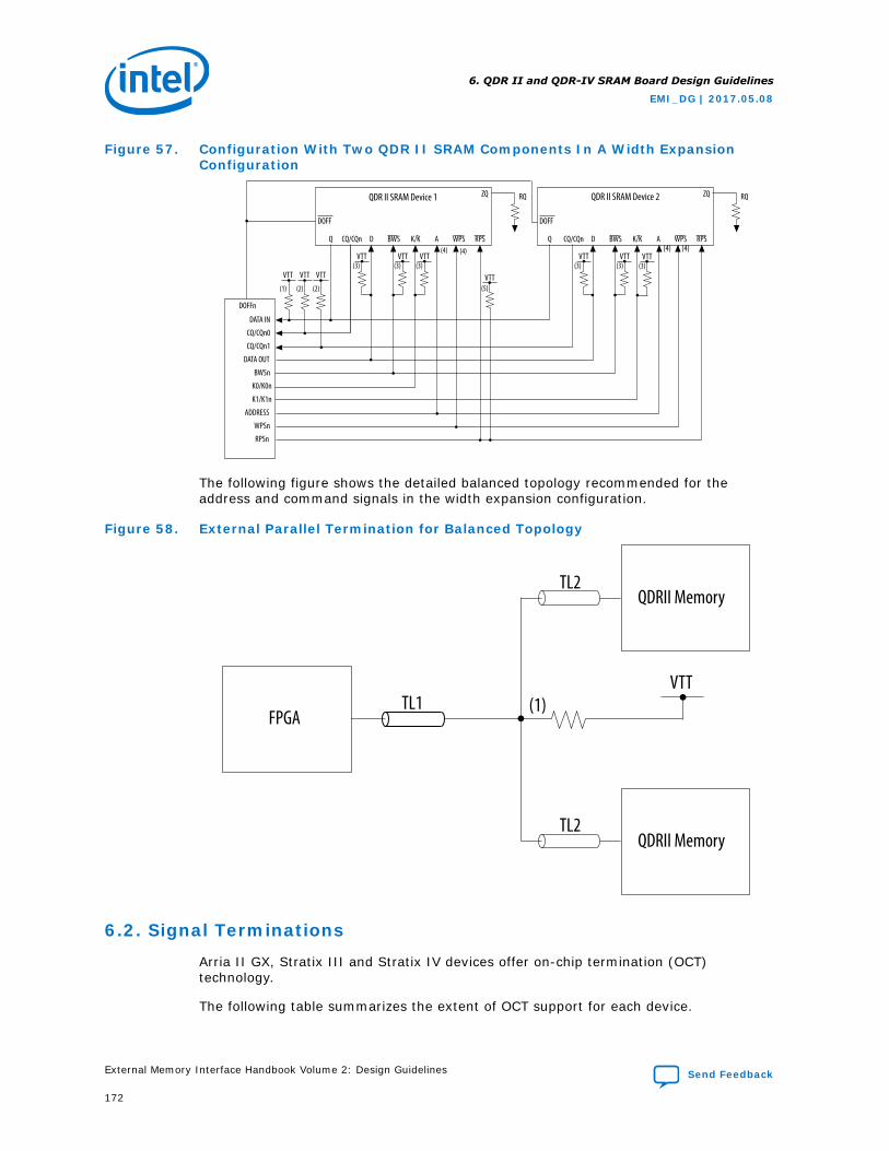
Figure 57. Configuration With Two QDR II SRAM Components In A Width ExpansionConfiguration
DOFFn
DATA IN
(1) (2) (2)
(3) (3) (3) (3)
CQ/CQn0
CQ/CQn1
DATA OUT
BWSn
K0/K0n
K1/K1n
ADDRESS
WPSn
RPSn
VTT
QDR II SRAM Device 1
DOFF
ZQ RQ
Q CQ/CQn D BWS K/K A WPS RPS
VTTVTT VTTVTT
QDR II SRAM Device 2
DOFF
ZQ RQ
Q CQ/CQn D BWS K/K A WPS RPS
VTT(3)
(4) (4) (4) (4)VTT
(5)VTT
(3)VTT
VTT
The following figure shows the detailed balanced topology recommended for theaddress and command signals in the width expansion configuration.
Figure 58. External Parallel Termination for Balanced Topology
TL1VTT
(1)
TL2
TL2
FPGA
QDRII Memory
QDRII Memory
6.2. Signal Terminations
Arria II GX, Stratix III and Stratix IV devices offer on-chip termination (OCT)technology.
The following table summarizes the extent of OCT support for each device.
6. QDR II and QDR-IV SRAM Board Design Guidelines
EMI_DG | 2017.05.08
External Memory Interface Handbook Volume 2: Design Guidelines Send Feedback
172
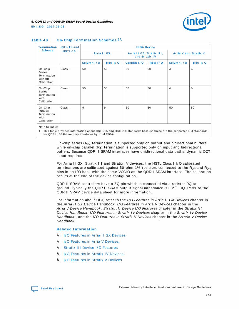
Table 48. On-Chip Termination Schemes (1)
TerminationScheme
HSTL-15 andHSTL-18
FPGA Device
Arria II GX Arria II GZ, Stratix III,and Stratix IV
Arria V and Stratix V
Column I/O Row I/O Column I/O Row I/O Column I/O Row I/O
On-ChipSeriesTerminationwithoutCalibration
Class I 50 50 50 50 — —
On-ChipSeriesTerminationwithCalibration
Class I 50 50 50 50 — —
On-ChipParallelTerminationwithCalibration
Class I — — 50 50 50 50
Note to Table:1. This table provides information about HSTL-15 and HSTL-18 standards because these are the supported I/O standards
for QDR II SRAM memory interfaces by Intel FPGAs.
On-chip series (RS) termination is supported only on output and bidirectional buffers,while on-chip parallel (RT) termination is supported only on input and bidirectionalbuffers. Because QDR II SRAM interfaces have unidirectional data paths, dynamic OCTis not required.
For Arria II GX, Stratix III and Stratix IV devices, the HSTL Class I I/O calibratedterminations are calibrated against 50-ohm 1% resistors connected to the RUP and RDNpins in an I/O bank with the same VCCIO as the QDRII SRAM interface. The calibrationoccurs at the end of the device configuration.
QDR II SRAM controllers have a ZQ pin which is connected via a resistor RQ toground. Typically the QDR II SRAM output signal impedance is 0.2 × RQ. Refer to theQDR II SRAM device data sheet for more information.
For information about OCT, refer to the I/O Features in Arria II GX Devices chapter inthe Arria II GX Device Handbook, I/O Features in Arria V Devices chapter in theArria V Device Handbook, Stratix III Device I/O Features chapter in the Stratix IIIDevice Handbook, I/O Features in Stratix IV Devices chapter in the Stratix IV DeviceHandbook , and the I/O Features in Stratix V Devices chapter in the Stratix V DeviceHandbook .
Related Information
• I/O Features in Arria II GX Devices
• I/O Features in Arria V Devices
• Stratix III Device I/O Features
• I/O Features in Stratix IV Devices
• I/O Features in Stratix V Devices
6. QDR II and QDR-IV SRAM Board Design Guidelines
EMI_DG | 2017.05.08
Send Feedback External Memory Interface Handbook Volume 2: Design Guidelines
173
6.2.1. Output from the FPGA to the QDR II SRAM Component
The following output signals are from the FPGA to the QDR II SRAM component:
• write data
• byte write select (BWSn)
• address
• control (WPSn and RPSn)
• clocks, K/K#
Intel recommends that you terminate the write clocks, K and K#, with a single-endedfly-by 50-ohmparallel termination to VTT. However, simulations show that you canconsider a differential termination if the clock pair is well matched and routeddifferentially.
Intel strongly recommends signal terminations to optimize signal integrity and timingmargins, and to minimize unwanted emissions, reflections, and crosstalk.
For point-to-point signals, Intel recommends that you place a fly-by termination byterminating at the end of the transmission line after the receiver to avoidunterminated stubs. The guideline is to place the fly-by termination within 100 pspropagation delay of the receiver.
Although not recommended, you can place the termination before the receiver, whichleaves an unterminated stub. The stub delay is critical because the stub between thetermination and the receiver is effectively unterminated, causing additional ringingand reflections. Stub delays should be less than 50 ps.
Note: Simulate your design to ensure correct functionality.
6.2.2. Input to the FPGA from the QDR II SRAM Component
The QDR II SRAM component drives the following input signals into the FPGA:
• read data
• echo clocks, CQ/CQ#
For point-to-point signals, Intel recommends that you use the FPGA parallel OCTwherever possible. For devices that do not support parallel OCT (Arria II GX), and for×36 emulated configuration CQ/CQ# termination, Intel recommends that you use afly-by 50-ohm parallel termination to VTT. Although not recommended, you can useparallel termination with a short stub of less that 50 ps propagation delay as analternative option. The input echo clocks, CQ and CQ# must not use a differentialtermination.
6.2.3. Termination Schemes
The following tables list the recommended termination schemes for major QDR IISRAM memory interface signals.
These signals include write data (D), byte write select (BWS), read data (Q), clocks (K,K#, CQ, and CQ#), address and command (WPS and RPS).
6. QDR II and QDR-IV SRAM Board Design Guidelines
EMI_DG | 2017.05.08
External Memory Interface Handbook Volume 2: Design Guidelines Send Feedback
174
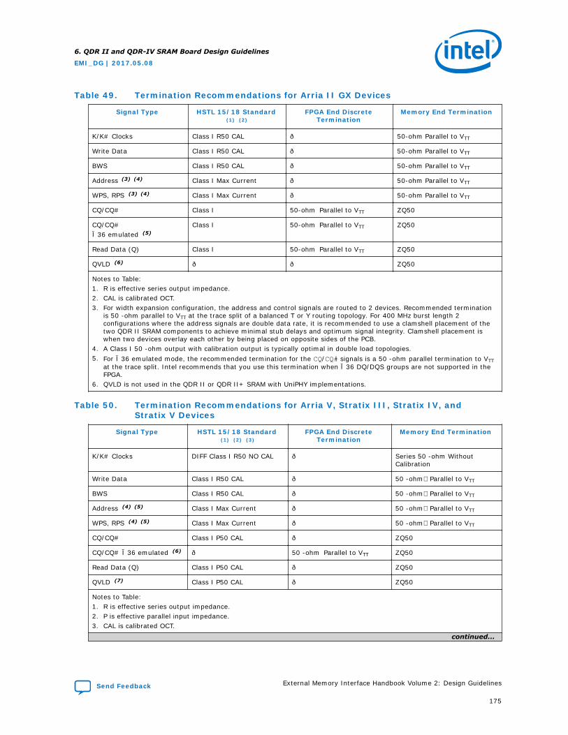
Table 49. Termination Recommendations for Arria II GX Devices
Signal Type HSTL 15/18 Standard (1) (2)
FPGA End DiscreteTermination
Memory End Termination
K/K# Clocks Class I R50 CAL — 50-ohm Parallel to VTT
Write Data Class I R50 CAL — 50-ohm Parallel to VTT
BWS Class I R50 CAL — 50-ohm Parallel to VTT
Address (3) (4) Class I Max Current — 50-ohm Parallel to VTT
WPS, RPS (3) (4) Class I Max Current — 50-ohm Parallel to VTT
CQ/CQ# Class I 50-ohm Parallel to VTT ZQ50
CQ/CQ#×36 emulated (5)
Class I 50-ohm Parallel to VTT ZQ50
Read Data (Q) Class I 50-ohm Parallel to VTT ZQ50
QVLD (6) — — ZQ50
Notes to Table:1. R is effective series output impedance.2. CAL is calibrated OCT.3. For width expansion configuration, the address and control signals are routed to 2 devices. Recommended termination
is 50 -ohm parallel to VTT at the trace split of a balanced T or Y routing topology. For 400 MHz burst length 2configurations where the address signals are double data rate, it is recommended to use a clamshell placement of thetwo QDR II SRAM components to achieve minimal stub delays and optimum signal integrity. Clamshell placement iswhen two devices overlay each other by being placed on opposite sides of the PCB.
4. A Class I 50 -ohm output with calibration output is typically optimal in double load topologies.5. For ×36 emulated mode, the recommended termination for the CQ/CQ# signals is a 50 -ohm parallel termination to VTT
at the trace split. Intel recommends that you use this termination when ×36 DQ/DQS groups are not supported in theFPGA.
6. QVLD is not used in the QDR II or QDR II+ SRAM with UniPHY implementations.
Table 50. Termination Recommendations for Arria V, Stratix III, Stratix IV, andStratix V Devices
Signal Type HSTL 15/18 Standard (1) (2) (3)
FPGA End DiscreteTermination
Memory End Termination
K/K# Clocks DIFF Class I R50 NO CAL — Series 50 -ohm WithoutCalibration
Write Data Class I R50 CAL — 50 -ohmParallel to VTT
BWS Class I R50 CAL — 50 -ohmParallel to VTT
Address (4) (5) Class I Max Current — 50 -ohmParallel to VTT
WPS, RPS (4) (5) Class I Max Current — 50 -ohmParallel to VTT
CQ/CQ# Class I P50 CAL — ZQ50
CQ/CQ# ×36 emulated (6) — 50 -ohm Parallel to VTT ZQ50
Read Data (Q) Class I P50 CAL — ZQ50
QVLD (7) Class I P50 CAL — ZQ50
Notes to Table:1. R is effective series output impedance.2. P is effective parallel input impedance.3. CAL is calibrated OCT.
continued...
6. QDR II and QDR-IV SRAM Board Design Guidelines
EMI_DG | 2017.05.08
Send Feedback External Memory Interface Handbook Volume 2: Design Guidelines
175
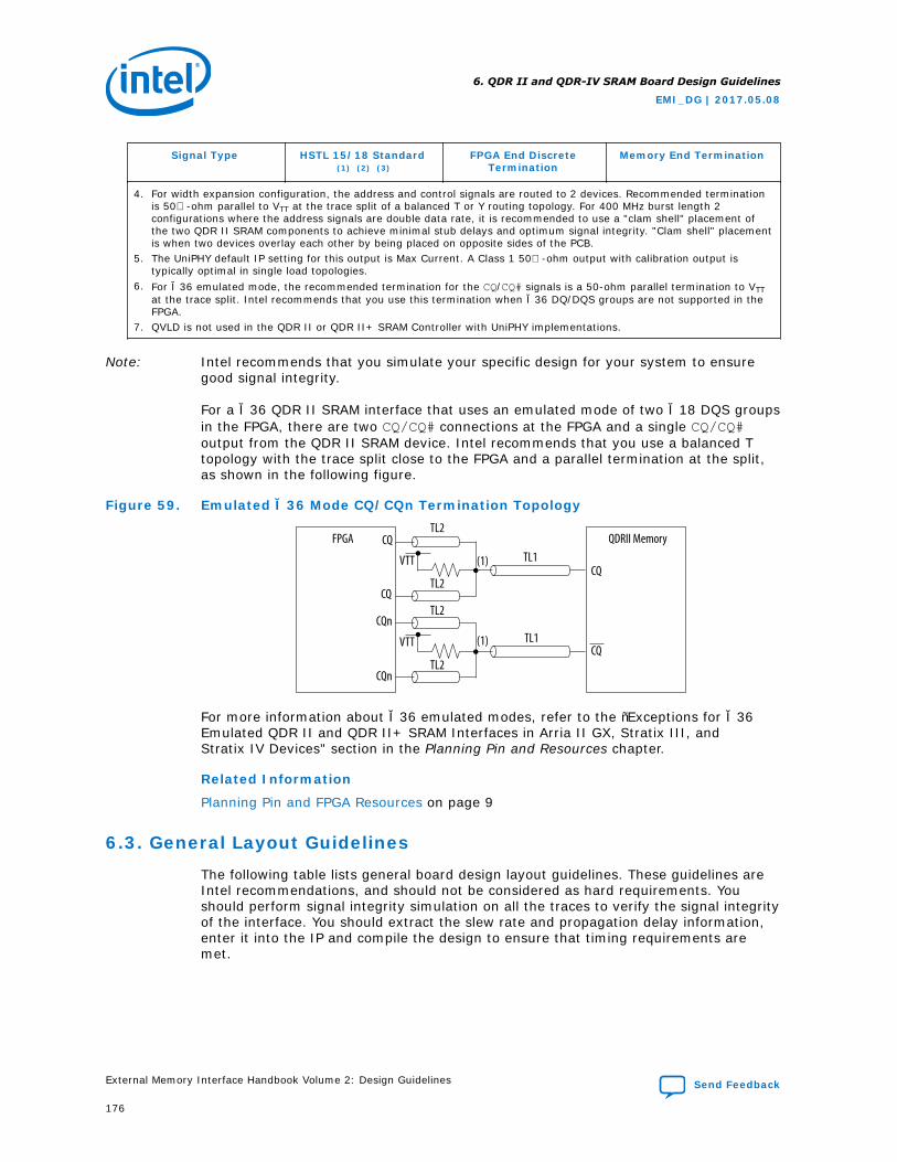
Signal Type HSTL 15/18 Standard (1) (2) (3)
FPGA End DiscreteTermination
Memory End Termination
4. For width expansion configuration, the address and control signals are routed to 2 devices. Recommended terminationis 50-ohm parallel to VTT at the trace split of a balanced T or Y routing topology. For 400 MHz burst length 2configurations where the address signals are double data rate, it is recommended to use a "clam shell" placement ofthe two QDR II SRAM components to achieve minimal stub delays and optimum signal integrity. "Clam shell" placementis when two devices overlay each other by being placed on opposite sides of the PCB.
5. The UniPHY default IP setting for this output is Max Current. A Class 1 50-ohm output with calibration output istypically optimal in single load topologies.
6. For ×36 emulated mode, the recommended termination for the CQ/CQ# signals is a 50-ohm parallel termination to VTTat the trace split. Intel recommends that you use this termination when ×36 DQ/DQS groups are not supported in theFPGA.
7. QVLD is not used in the QDR II or QDR II+ SRAM Controller with UniPHY implementations.
Note: Intel recommends that you simulate your specific design for your system to ensuregood signal integrity.
For a ×36 QDR II SRAM interface that uses an emulated mode of two ×18 DQS groupsin the FPGA, there are two CQ/CQ# connections at the FPGA and a single CQ/CQ#output from the QDR II SRAM device. Intel recommends that you use a balanced Ttopology with the trace split close to the FPGA and a parallel termination at the split,as shown in the following figure.
Figure 59. Emulated ×36 Mode CQ/CQn Termination Topology
FPGATL2
TL1
TL1
CQ
CQ
CQ
CQn
CQn
CQ
TL2
TL2
TL2
(1)
(1)
VTT
VTT
QDRII Memory
For more information about ×36 emulated modes, refer to the “Exceptions for ×36Emulated QDR II and QDR II+ SRAM Interfaces in Arria II GX, Stratix III, andStratix IV Devices" section in the Planning Pin and Resources chapter.
Related Information
Planning Pin and FPGA Resources on page 9
6.3. General Layout Guidelines
The following table lists general board design layout guidelines. These guidelines areIntel recommendations, and should not be considered as hard requirements. Youshould perform signal integrity simulation on all the traces to verify the signal integrityof the interface. You should extract the slew rate and propagation delay information,enter it into the IP and compile the design to ensure that timing requirements aremet.
6. QDR II and QDR-IV SRAM Board Design Guidelines
EMI_DG | 2017.05.08
External Memory Interface Handbook Volume 2: Design Guidelines Send Feedback
176
Table 51. General Layout Guidelines
Parameter Guidelines
Impedance • All unused via pads must be removed, because they cause unwantedcapacitance.
• Trace impedance plays an important role in the signal integrity. You mustperform board level simulation to determine the best characteristic impedancefor your PCB. For example, it is possible that for multi rank systems 40 ohmscould yield better results than a traditional 50 ohm characteristic impedance.
Decoupling Parameter • Use 0.1 uF in 0402 size to minimize inductance• Make VTT voltage decoupling close to termination resistors• Connect decoupling caps between VTT and ground• Use a 0.1 uF cap for every other VTT pin and 0.01 uF cap for every VDD and
VDDQ pin• Verify the capacitive decoupling using the Intel Power Distribution Network
Design Tool
Power • Route GND and VCC as planes• Route VCCIO for memories in a single split plane with at least a 20-mil
(0.020 inches, or 0.508 mm) gap of separation• Route VTT as islands or 250-mil (6.35-mm) power traces• Route oscillators and PLL power as islands or 100-mil (2.54-mm) power traces
General Routing All specified delay matching requirements include PCB trace delays, different layerpropagation velocity variance, and crosstalk. To minimize PCB layer propogationvariance, Intel recommends that signals from the same net group always berouted on the same layer.• Use 45° angles (not 90° corners)• Avoid T-Junctions for critical nets or clocks• Avoid T-junctions greater than 250 mils (6.35 mm)• Disallow signals across split planes• Restrict routing other signals close to system reset signals• Avoid routing memory signals closer than 0.025 inch (0.635 mm) to PCI or
system clocks
Related Information
Power Distribution Network Design Tool
6.4. QDR II Layout Guidelines
The following table summarizes QDR II and QDR II SRAM general routing layoutguidelines.
Note: 1. The following layout guidelines include several +/- length based rules. Theselength based guidelines are for first order timing approximations if you cannotsimulate the actual delay characteristics of your PCB implementation. They do notinclude any margin for crosstalk.
2. Intel recommends that you get accurate time base skew numbers when yousimulate your specific implementation.
3. To reliably close timing to and from the periphery of the device, signals to andfrom the periphery should be registered before any further logic is connected.
6. QDR II and QDR-IV SRAM Board Design Guidelines
EMI_DG | 2017.05.08
Send Feedback External Memory Interface Handbook Volume 2: Design Guidelines
177
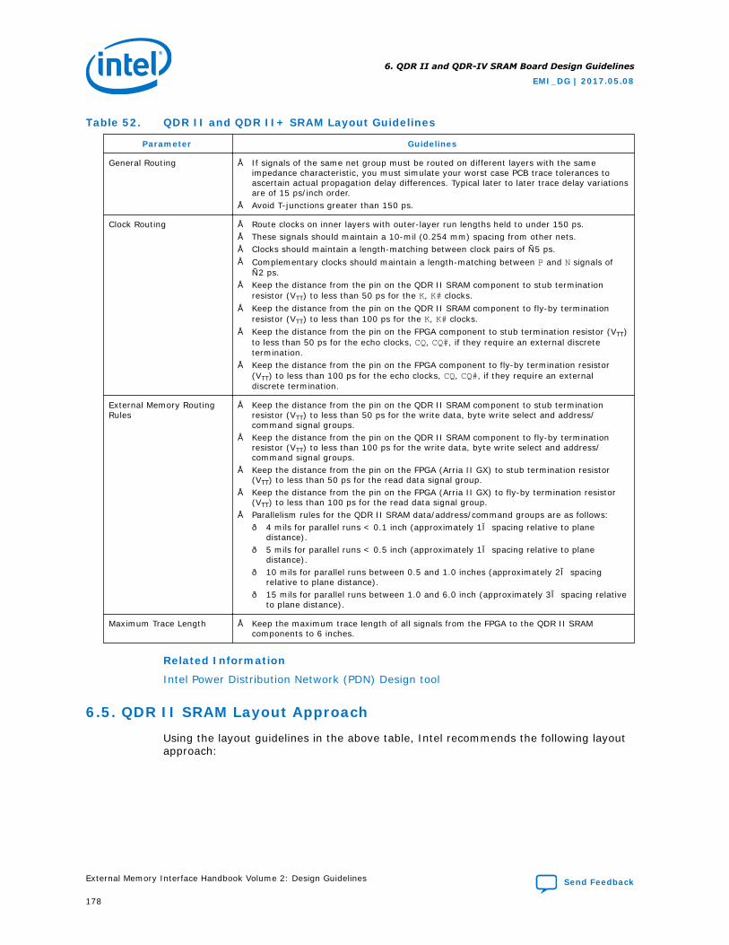
Table 52. QDR II and QDR II+ SRAM Layout Guidelines
Parameter Guidelines
General Routing • If signals of the same net group must be routed on different layers with the sameimpedance characteristic, you must simulate your worst case PCB trace tolerances toascertain actual propagation delay differences. Typical later to later trace delay variationsare of 15 ps/inch order.
• Avoid T-junctions greater than 150 ps.
Clock Routing • Route clocks on inner layers with outer-layer run lengths held to under 150 ps.• These signals should maintain a 10-mil (0.254 mm) spacing from other nets.• Clocks should maintain a length-matching between clock pairs of ±5 ps.• Complementary clocks should maintain a length-matching between P and N signals of
±2 ps.• Keep the distance from the pin on the QDR II SRAM component to stub termination
resistor (VTT) to less than 50 ps for the K, K# clocks.• Keep the distance from the pin on the QDR II SRAM component to fly-by termination
resistor (VTT) to less than 100 ps for the K, K# clocks.• Keep the distance from the pin on the FPGA component to stub termination resistor (VTT)
to less than 50 ps for the echo clocks, CQ, CQ#, if they require an external discretetermination.
• Keep the distance from the pin on the FPGA component to fly-by termination resistor(VTT) to less than 100 ps for the echo clocks, CQ, CQ#, if they require an externaldiscrete termination.
External Memory RoutingRules
• Keep the distance from the pin on the QDR II SRAM component to stub terminationresistor (VTT) to less than 50 ps for the write data, byte write select and address/command signal groups.
• Keep the distance from the pin on the QDR II SRAM component to fly-by terminationresistor (VTT) to less than 100 ps for the write data, byte write select and address/command signal groups.
• Keep the distance from the pin on the FPGA (Arria II GX) to stub termination resistor(VTT) to less than 50 ps for the read data signal group.
• Keep the distance from the pin on the FPGA (Arria II GX) to fly-by termination resistor(VTT) to less than 100 ps for the read data signal group.
• Parallelism rules for the QDR II SRAM data/address/command groups are as follows:— 4 mils for parallel runs < 0.1 inch (approximately 1× spacing relative to plane
distance).— 5 mils for parallel runs < 0.5 inch (approximately 1× spacing relative to plane
distance).— 10 mils for parallel runs between 0.5 and 1.0 inches (approximately 2× spacing
relative to plane distance).— 15 mils for parallel runs between 1.0 and 6.0 inch (approximately 3× spacing relative
to plane distance).
Maximum Trace Length • Keep the maximum trace length of all signals from the FPGA to the QDR II SRAMcomponents to 6 inches.
Related Information
Intel Power Distribution Network (PDN) Design tool
6.5. QDR II SRAM Layout Approach
Using the layout guidelines in the above table, Intel recommends the following layoutapproach:
6. QDR II and QDR-IV SRAM Board Design Guidelines
EMI_DG | 2017.05.08
External Memory Interface Handbook Volume 2: Design Guidelines Send Feedback
178
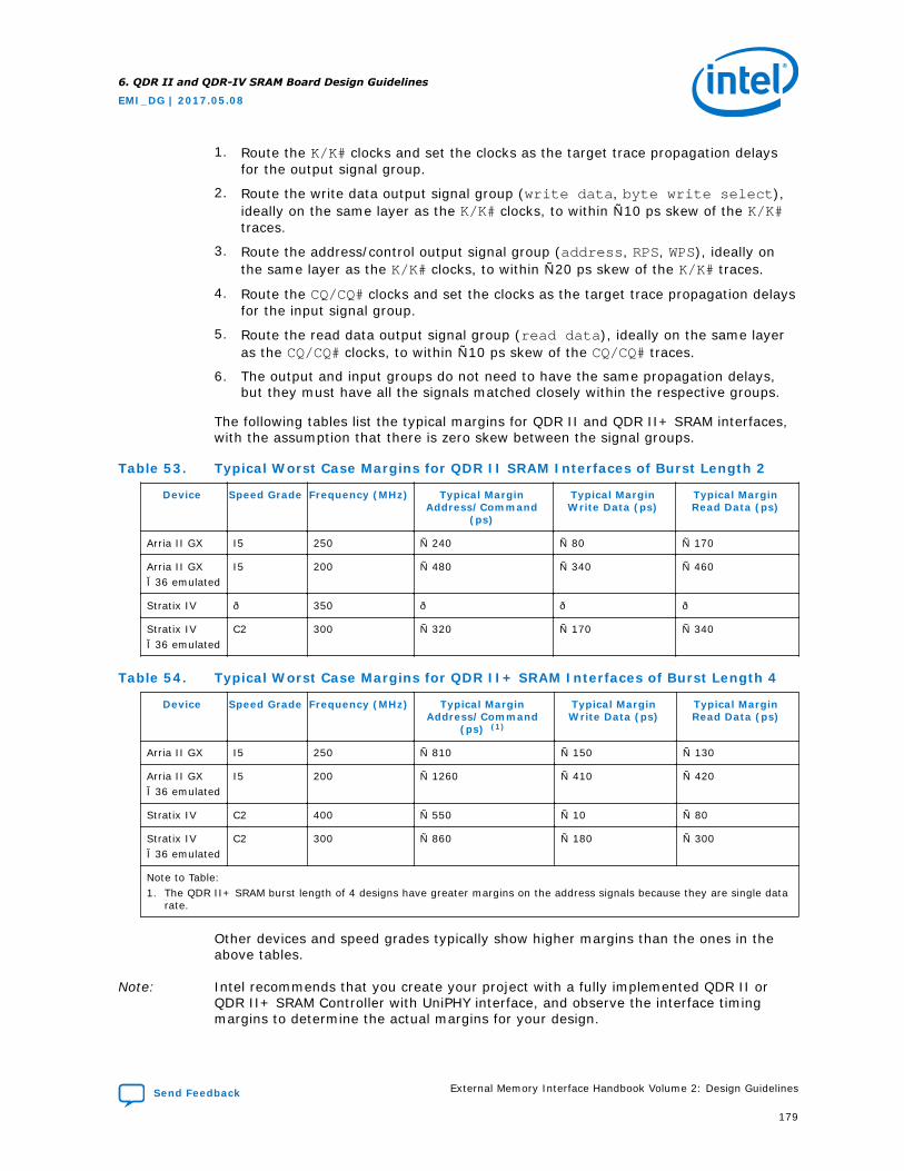
1. Route the K/K# clocks and set the clocks as the target trace propagation delaysfor the output signal group.
2. Route the write data output signal group (write data, byte write select),ideally on the same layer as the K/K# clocks, to within ±10 ps skew of the K/K#traces.
3. Route the address/control output signal group (address, RPS, WPS), ideally onthe same layer as the K/K# clocks, to within ±20 ps skew of the K/K# traces.
4. Route the CQ/CQ# clocks and set the clocks as the target trace propagation delaysfor the input signal group.
5. Route the read data output signal group (read data), ideally on the same layeras the CQ/CQ# clocks, to within ±10 ps skew of the CQ/CQ# traces.
6. The output and input groups do not need to have the same propagation delays,but they must have all the signals matched closely within the respective groups.
The following tables list the typical margins for QDR II and QDR II+ SRAM interfaces,with the assumption that there is zero skew between the signal groups.
Table 53. Typical Worst Case Margins for QDR II SRAM Interfaces of Burst Length 2
Device Speed Grade Frequency (MHz) Typical MarginAddress/Command
(ps)
Typical MarginWrite Data (ps)
Typical MarginRead Data (ps)
Arria II GX I5 250 ± 240 ± 80 ± 170
Arria II GX×36 emulated
I5 200 ± 480 ± 340 ± 460
Stratix IV — 350 — — —
Stratix IV×36 emulated
C2 300 ± 320 ± 170 ± 340
Table 54. Typical Worst Case Margins for QDR II+ SRAM Interfaces of Burst Length 4
Device Speed Grade Frequency (MHz) Typical MarginAddress/Command
(ps) (1)
Typical MarginWrite Data (ps)
Typical MarginRead Data (ps)
Arria II GX I5 250 ± 810 ± 150 ± 130
Arria II GX×36 emulated
I5 200 ± 1260 ± 410 ± 420
Stratix IV C2 400 ± 550 ± 10 ± 80
Stratix IV×36 emulated
C2 300 ± 860 ± 180 ± 300
Note to Table:1. The QDR II+ SRAM burst length of 4 designs have greater margins on the address signals because they are single data
rate.
Other devices and speed grades typically show higher margins than the ones in theabove tables.
Note: Intel recommends that you create your project with a fully implemented QDR II orQDR II+ SRAM Controller with UniPHY interface, and observe the interface timingmargins to determine the actual margins for your design.
6. QDR II and QDR-IV SRAM Board Design Guidelines
EMI_DG | 2017.05.08
Send Feedback External Memory Interface Handbook Volume 2: Design Guidelines
179
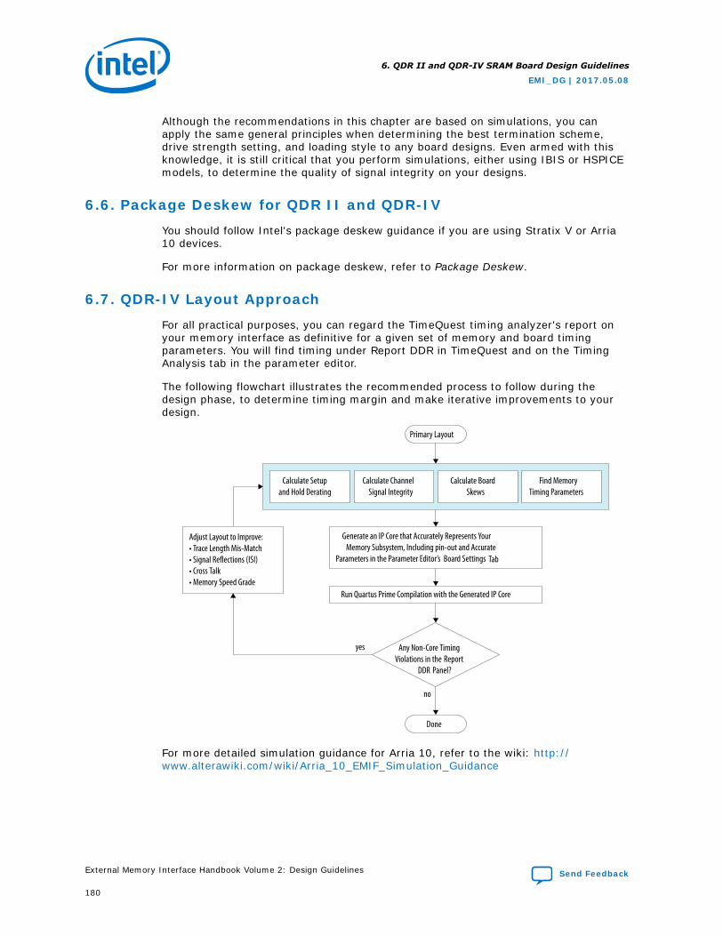
Although the recommendations in this chapter are based on simulations, you canapply the same general principles when determining the best termination scheme,drive strength setting, and loading style to any board designs. Even armed with thisknowledge, it is still critical that you perform simulations, either using IBIS or HSPICEmodels, to determine the quality of signal integrity on your designs.
6.6. Package Deskew for QDR II and QDR-IV
You should follow Intel's package deskew guidance if you are using Stratix V or Arria10 devices.
For more information on package deskew, refer to Package Deskew.
6.7. QDR-IV Layout Approach
For all practical purposes, you can regard the TimeQuest timing analyzer's report onyour memory interface as definitive for a given set of memory and board timingparameters. You will find timing under Report DDR in TimeQuest and on the TimingAnalysis tab in the parameter editor.
The following flowchart illustrates the recommended process to follow during thedesign phase, to determine timing margin and make iterative improvements to yourdesign.
Primary Layout
Calculate Setupand Hold Derating
Calculate ChannelSignal Integrity
Calculate BoardSkews
Find MemoryTiming Parameters
Generate an IP Core that Accurately Represents Your Memory Subsystem, Including pin-out and Accurate
Parameters in the Parameter Editor’s Board Settings Tab
Run Quartus Prime Compilation with the Generated IP Core
Any Non-Core TimingViolations in the Report
DDR Panel?
yes
no
Done
Adjust Layout to Improve:• Trace Length Mis-Match• Signal Reflections (ISI)• Cross Talk• Memory Speed Grade
For more detailed simulation guidance for Arria 10, refer to the wiki: http://www.alterawiki.com/wiki/Arria_10_EMIF_Simulation_Guidance
6. QDR II and QDR-IV SRAM Board Design Guidelines
EMI_DG | 2017.05.08
External Memory Interface Handbook Volume 2: Design Guidelines Send Feedback
180
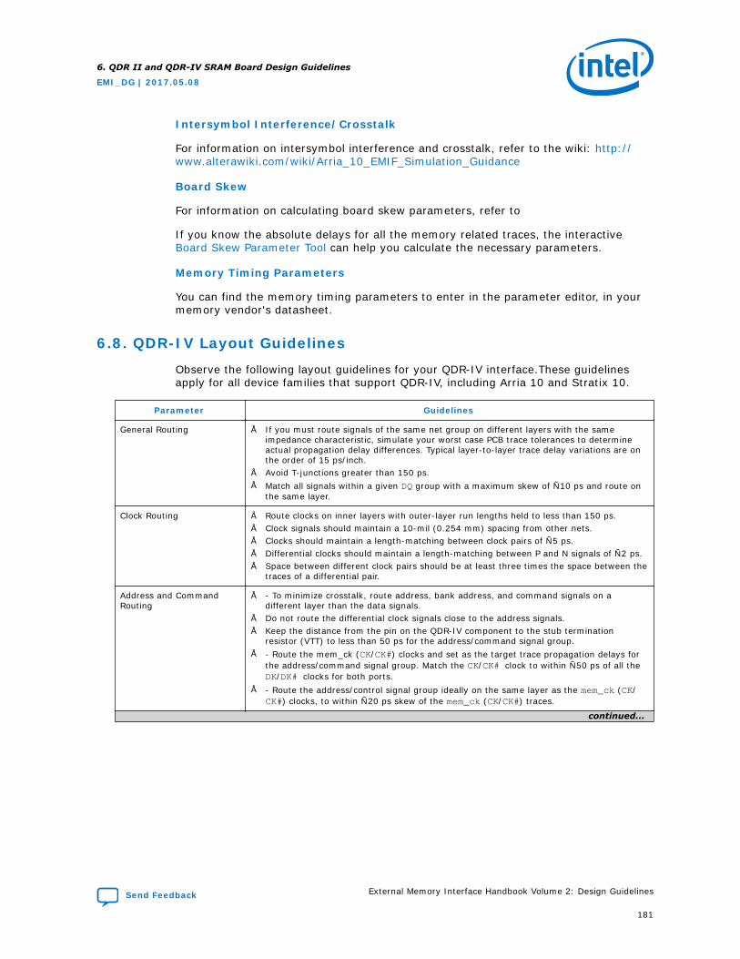
Intersymbol Interference/Crosstalk
For information on intersymbol interference and crosstalk, refer to the wiki: http://www.alterawiki.com/wiki/Arria_10_EMIF_Simulation_Guidance
Board Skew
For information on calculating board skew parameters, refer to
If you know the absolute delays for all the memory related traces, the interactive Board Skew Parameter Tool can help you calculate the necessary parameters.
Memory Timing Parameters
You can find the memory timing parameters to enter in the parameter editor, in yourmemory vendor's datasheet.
6.8. QDR-IV Layout Guidelines
Observe the following layout guidelines for your QDR-IV interface.These guidelinesapply for all device families that support QDR-IV, including Arria 10 and Stratix 10.
Parameter Guidelines
General Routing • If you must route signals of the same net group on different layers with the sameimpedance characteristic, simulate your worst case PCB trace tolerances to determineactual propagation delay differences. Typical layer-to-layer trace delay variations are onthe order of 15 ps/inch.
• Avoid T-junctions greater than 150 ps.• Match all signals within a given DQ group with a maximum skew of ±10 ps and route on
the same layer.
Clock Routing • Route clocks on inner layers with outer-layer run lengths held to less than 150 ps.• Clock signals should maintain a 10-mil (0.254 mm) spacing from other nets.• Clocks should maintain a length-matching between clock pairs of ±5 ps.• Differential clocks should maintain a length-matching between P and N signals of ±2 ps.• Space between different clock pairs should be at least three times the space between the
traces of a differential pair.
Address and CommandRouting
• - To minimize crosstalk, route address, bank address, and command signals on adifferent layer than the data signals.
• Do not route the differential clock signals close to the address signals.• Keep the distance from the pin on the QDR-IV component to the stub termination
resistor (VTT) to less than 50 ps for the address/command signal group.• - Route the mem_ck (CK/CK#) clocks and set as the target trace propagation delays for
the address/command signal group. Match the CK/CK# clock to within ±50 ps of all theDK/DK# clocks for both ports.
• - Route the address/control signal group ideally on the same layer as the mem_ck (CK/CK#) clocks, to within ±20 ps skew of the mem_ck (CK/CK#) traces.
continued...
6. QDR II and QDR-IV SRAM Board Design Guidelines
EMI_DG | 2017.05.08
Send Feedback External Memory Interface Handbook Volume 2: Design Guidelines
181
Parameter Guidelines
Data Signals • For port B only: Swap the polarity of the QKB and QKB# signals with respect to thepolarity of the differential buffer inputs on the FPGA. Connect the positive leg of thedifferential input buffer on the FPGA to QDR-IV QKB# (negative) pin and vice-versa. Notethat the port names at the top-level of the IP already reflect this swap (that is, mem_qkbis assigned to the negative buffer leg, and mem_qkb_n is assigned to the positive bufferleg).
• For each port, route the DK/DK# write clock and QK/QK# read clock associated with a DQgroup on the same PCB layer. Match these clock pairs to within ±5 ps.
• For each port, set the DK/DK# or QK/QK# clock as the target trace propagation delay forthe associated data signals (DQ).
• For each port, route the data (DQ) signals for the DQ group ideally on the same layer asthe associated QK/QK# and DK/DK# clocks to within ±10 ps skew of the target clock.
Maximum Trace Length • Keep the maximum trace length of all signals from the FPGA to the QDR-IV componentsto 600 ps.
Spacing Guidelines • Avoid routing two signal layers next to each other. Always make sure that the signalsrelated to memory interface are routed between appropriate GND or power layers.
• For Data and Data Strobe traces: Maintain at least 3H spacing between the edges (air-gap) of these traces, where H is the vertical distance to the closest return path for thatparticular trace.
• For Address/Command/Control traces: Maintain at least 3H spacing between the edges(air-gap) of these traces, where H is the vertical distance to the closest return path forthat particular trace.
• For Clock (mem_CK) traces: Maintain at least 5H spacing between two clock pair or aclock pair and any other memory interface trace, where H is the vertical distance to theclosest return path for that particular trace.
Trace Matching Guidance The following layout approach is recommended, based on the preceding guidelines:1. For port B only: Swap the polarity of the QKB and QKB# signals with respect to the
polarity of the differential buffer inputs on the FPGA. Connect the positive leg of thedifferential input buffer on the FPGA to QDR-IV QKB# (negative) pin and vice-versa. Notethat the port names at the top-level of the IP already reflect this swap (that is, mem_qkbis assigned to the negative buffer leg, and mem_qkb_n is assigned to the positive bufferleg).
2. For each port, set the DK/DK# or QK/QK# clock as the target trace propagation delay forthe associated data signals (DQ).
3. For each port, route the data (DQ) signals for the DQ group ideally on the same layer asthe associated QK/QK# and DK/DK# clocks to within ±10 ps skew of the target clock.
4. Route the mem_ck (CK/CK#) clocks and set as the target trace propagation delays for theaddress/command signal group. Match the CK/CK# clock to within ±50 ps of all theDK/DK# clocks for both ports.
5. Route theaddress/control signal group ideally on the same layer as the mem_ck (CK/CK#) clocks, to within ±10 ps skew of the mem_ck (CK/CK#) traces.
6.9. Document Revision History
Date Version Changes
May 2017 2017.5.08 • Added Stratix 10 to QDR-IV Layout Guidelines section.• Rebranded as Intel.
October 2016 2016.10.31 Maintenance release.
May 2016 2016.05.02 Maintenance release.
November 2015 2015.11.02 Maintenance release.
May 2015 2015.05.04 In the first guideline of the QDR-IV Layout Recommendations and the DataSignals section of the QDR-IV Layout Guidelines, revised the information forPort B only.
continued...
6. QDR II and QDR-IV SRAM Board Design Guidelines
EMI_DG | 2017.05.08
External Memory Interface Handbook Volume 2: Design Guidelines Send Feedback
182
Date Version Changes
December 2014 2014.12.15 Maintenance release.
August 2014 2014.08.15 • Change to K/K# Clocks row in Termination Recommendations for Arria V,Stratix III, Stratix IV, and Stratix V Devices table.
• Removed millimeter approximations from lengths expressed inpicoseconds in QDR II and QDR II+ SRAM Layout Guidelines table.
• Minor formatting fixes in QDR II and QDR II+ SRAM Layout Guidelinestable.
December 2013 2013.12.16 Consolidated General Layout Guidelines.
November 2012 4.2 Changed chapter number from 7 to 8.
June 2012 4.1 Added Feedback icon.
November 2011 4.0 Added Arria V information.
June 2011 3.0 Added Stratix V information.
December 2010 2.0 Maintenance release.
July 2010 1.0 Initial release.
6. QDR II and QDR-IV SRAM Board Design Guidelines
EMI_DG | 2017.05.08
Send Feedback External Memory Interface Handbook Volume 2: Design Guidelines
183
7. Implementing and Parameterizing Memory IPThe following topics describe the general overview of the IP core design flow to helpyou quickly get started with any IP core.
The IP Library is installed as part of the Quartus® Prime installation process.You canselect and parameterize any Intel® IP core from the library. Intel provides anintegrated parameter editor that allows you to customize IP cores to support a widevariety of applications. The parameter editor guides you through the setting ofparameter values and selection of optional ports. The following section describes thegeneral design flow and use of Intel® IP cores.
Note: Information for Arria 10 External Memory Interface IP also applies to Arria 10 ExternalMemory Interface for HPS IP unless stated otherwise.
Related Information
Intel FPGA Design StoreDesign Example for Arria 10 DDR3 External Memory Interface is available in theIntel FPGA Design Store.
7.1. Installing and Licensing IP Cores
The Intel Quartus Prime software installation includes the Intel FPGA IP library. Thislibrary provides useful IP core functions for your production use without the need foran additional license. Some IP cores in the library require that you purchase aseparate license for production use. The OpenCore® feature allows evaluation of anyIntel FPGA IP core in simulation and compilation in the Quartus Prime software. Uponsatisfaction with functionality and performance, visit the Self Service Licensing Centerto obtain a license number for any Intel FPGA product.
The Quartus Prime software installs IP cores in the following locations by default:
Figure 60. IP Core Installation Path
intelFPGA(_pro*)
quartus - Contains the Quartus Prime softwareip - Contains the IP library and third-party IP cores
altera - Contains the IP library source code<IP core name> - Contains the IP core source files
EMI_DG | 2017.05.08
Send Feedback
Intel Corporation. All rights reserved. Intel, the Intel logo, Altera, Arria, Cyclone, Enpirion, MAX, Nios, Quartusand Stratix words and logos are trademarks of Intel Corporation or its subsidiaries in the U.S. and/or othercountries. Intel warrants performance of its FPGA and semiconductor products to current specifications inaccordance with Intel's standard warranty, but reserves the right to make changes to any products and servicesat any time without notice. Intel assumes no responsibility or liability arising out of the application or use of anyinformation, product, or service described herein except as expressly agreed to in writing by Intel. Intelcustomers are advised to obtain the latest version of device specifications before relying on any publishedinformation and before placing orders for products or services.*Other names and brands may be claimed as the property of others.
ISO9001:2015Registered
Table 55. IP Core Installation Locations
Location Software Platform
<drive>:\intelFPGA_pro\quartus\ip\altera Quartus Prime Pro Edition Windows*
<drive>:\intelFPGA\quartus\ip\altera Quartus Prime Standard Edition Windows
<home directory>:/intelFPGA_pro/quartus/ip/altera Quartus Prime Pro Edition Linux*
<home directory>:/intelFPGA/quartus/ip/altera Quartus Prime Standard Edition Linux
7.2. Design Flow
You can implement the external memory interface IP using the following flows:
• IP Catalog flow
• Qsys flow
The following figure shows the stages for creating a system in the Quartus Primesoftware using the available flows.
7. Implementing and Parameterizing Memory IP
EMI_DG | 2017.05.08
Send Feedback External Memory Interface Handbook Volume 2: Design Guidelines
185
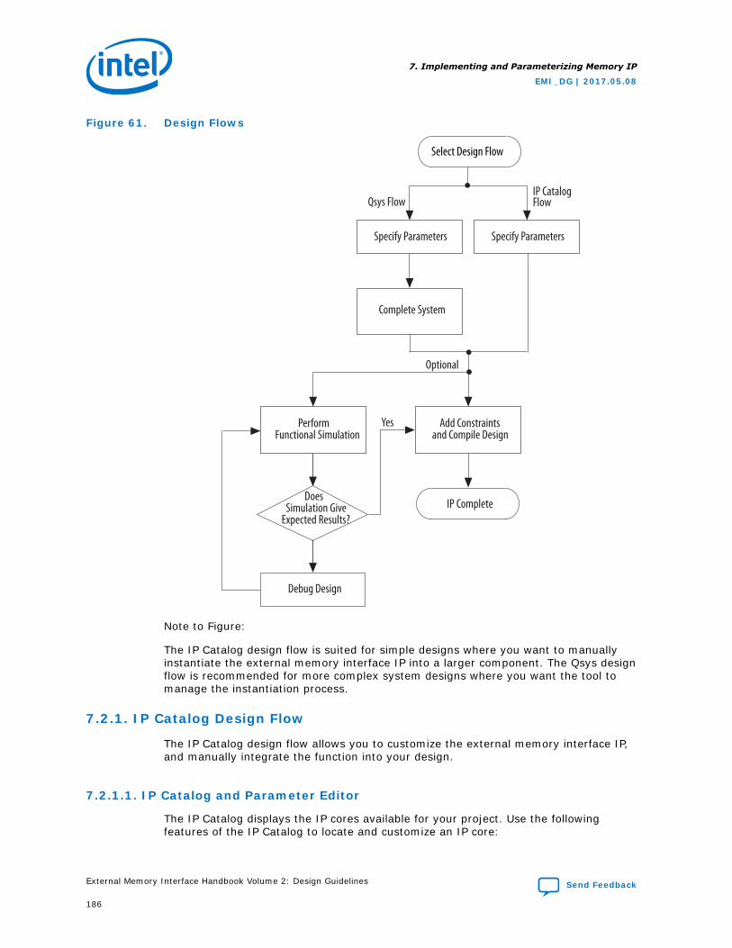
Figure 61. Design Flows
Select Design Flow
Specify Parameters
Qsys FlowIP CatalogFlow
Complete System
Specify Parameters
IP Complete
Add Constraintsand Compile Design
Perform Functional Simulation
Debug Design
Does Simulation Give
Expected Results?
Yes
Optional
Note to Figure:
The IP Catalog design flow is suited for simple designs where you want to manuallyinstantiate the external memory interface IP into a larger component. The Qsys designflow is recommended for more complex system designs where you want the tool tomanage the instantiation process.
7.2.1. IP Catalog Design Flow
The IP Catalog design flow allows you to customize the external memory interface IP,and manually integrate the function into your design.
7.2.1.1. IP Catalog and Parameter Editor
The IP Catalog displays the IP cores available for your project. Use the followingfeatures of the IP Catalog to locate and customize an IP core:
7. Implementing and Parameterizing Memory IP
EMI_DG | 2017.05.08
External Memory Interface Handbook Volume 2: Design Guidelines Send Feedback
186
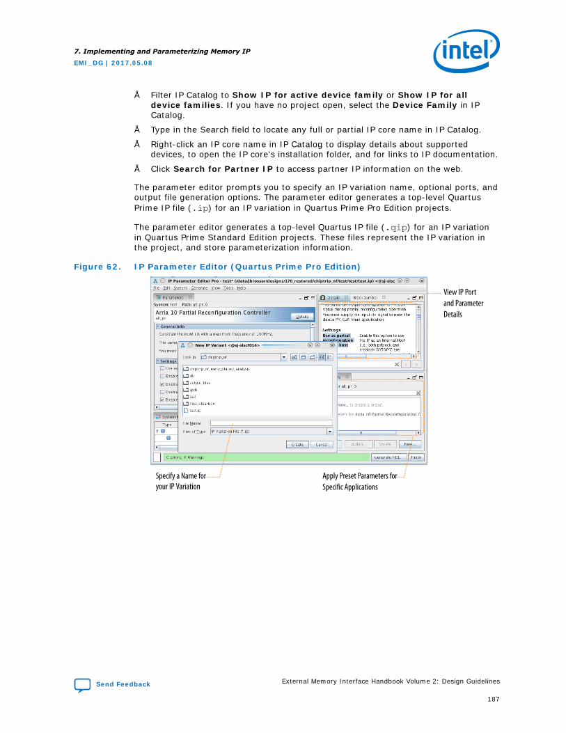
• Filter IP Catalog to Show IP for active device family or Show IP for alldevice families. If you have no project open, select the Device Family in IPCatalog.
• Type in the Search field to locate any full or partial IP core name in IP Catalog.
• Right-click an IP core name in IP Catalog to display details about supporteddevices, to open the IP core's installation folder, and for links to IP documentation.
• Click Search for Partner IP to access partner IP information on the web.
The parameter editor prompts you to specify an IP variation name, optional ports, andoutput file generation options. The parameter editor generates a top-level QuartusPrime IP file (.ip) for an IP variation in Quartus Prime Pro Edition projects.
The parameter editor generates a top-level Quartus IP file (.qip) for an IP variationin Quartus Prime Standard Edition projects. These files represent the IP variation inthe project, and store parameterization information.
Figure 62. IP Parameter Editor (Quartus Prime Pro Edition)
View IP Portand Parameter Details
Apply Preset Parameters forSpecific Applications
Specify a Name foryour IP Variation
7. Implementing and Parameterizing Memory IP
EMI_DG | 2017.05.08
Send Feedback External Memory Interface Handbook Volume 2: Design Guidelines
187
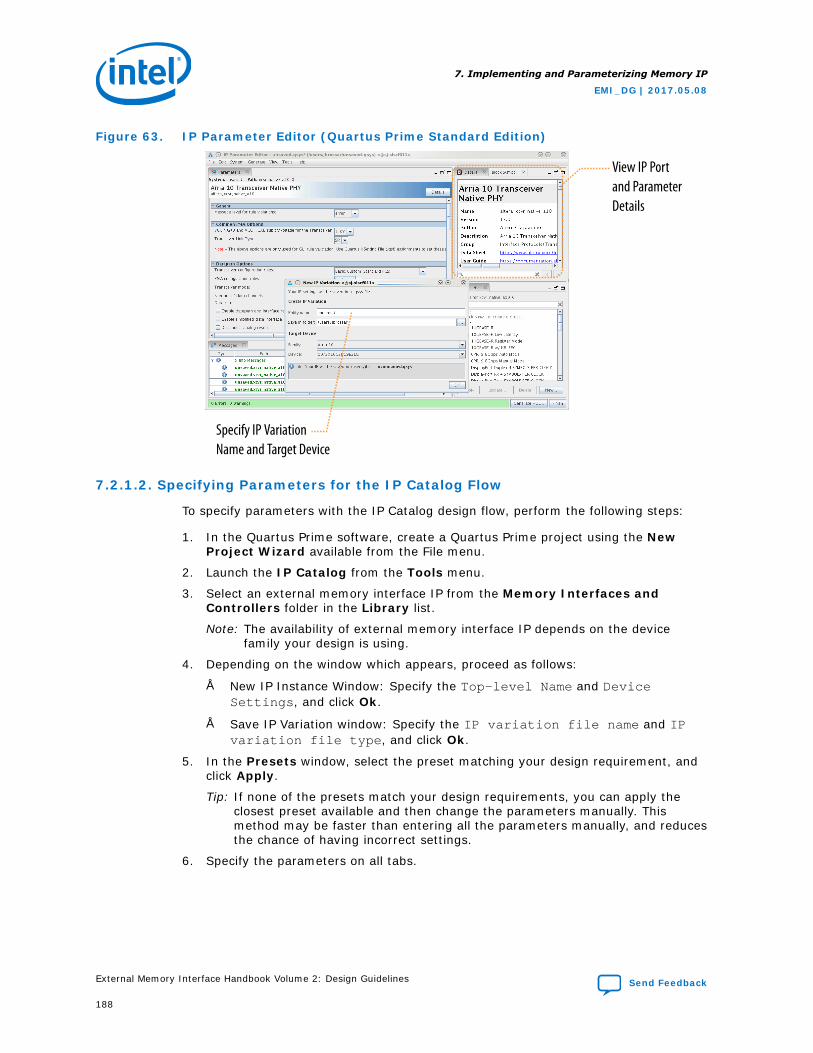
Figure 63. IP Parameter Editor (Quartus Prime Standard Edition)
View IP Portand Parameter Details
Specify IP VariationName and Target Device
7.2.1.2. Specifying Parameters for the IP Catalog Flow
To specify parameters with the IP Catalog design flow, perform the following steps:
1. In the Quartus Prime software, create a Quartus Prime project using the NewProject Wizard available from the File menu.
2. Launch the IP Catalog from the Tools menu.
3. Select an external memory interface IP from the Memory Interfaces andControllers folder in the Library list.
Note: The availability of external memory interface IP depends on the devicefamily your design is using.
4. Depending on the window which appears, proceed as follows:
• New IP Instance Window: Specify the Top-level Name and DeviceSettings, and click Ok.
• Save IP Variation window: Specify the IP variation file name and IPvariation file type, and click Ok.
5. In the Presets window, select the preset matching your design requirement, andclick Apply.
Tip: If none of the presets match your design requirements, you can apply theclosest preset available and then change the parameters manually. Thismethod may be faster than entering all the parameters manually, and reducesthe chance of having incorrect settings.
6. Specify the parameters on all tabs.
7. Implementing and Parameterizing Memory IP
EMI_DG | 2017.05.08
External Memory Interface Handbook Volume 2: Design Guidelines Send Feedback
188
Note: • For detailed explanation of the parameters, refer to ParameterizingMemory Controllers with UniPHY IP and Parameterizing MemoryControllers with Arria 10 External Memory Interface IP.
• Although you have applied presets, you may need to modify some of thepreset parameters depending on the frequency of operation. A typicallist of parameters which you might need to change includes the MemoryCAS Latency setting, the Memory CAS Write Latency setting, and thetWTR, tFAW, tRRD, and tRTP settings.
Tip: • As a good practice, review any warning messages displayed in theMessages Window and correct any errors before making furtherchanges.
• To simplify future work, you might want to store the current configurationby saving your own presets. To create, modify, or remove your owncustom presets, click New, Update, or Delete at the bottom of thePresets list.
• If you want to generate an example design for your current configuration,click Example Design at the top-right corner of the parameter editor,specify a path for the example design, and click Ok.
7. Depending on which external memory interface IP is selected, perform thefollowing steps to complete the IP generation:
7. Implementing and Parameterizing Memory IP
EMI_DG | 2017.05.08
Send Feedback External Memory Interface Handbook Volume 2: Design Guidelines
189

• For Arria 10 or Stratix 10 External Memory Interface IP:
a. Click Finish. Your configuration is saved as a .qsys file.
b. Click Yes when you are prompted to generate your IP.
c. Set Create HDL design files for synthesis to Verilog or VHDL.
Tip: If you want to do RTL simulation of your design, you should setCreate simulation model to either Verilog or VHDL. Some RTLsimulation-related files, including simulator-specific scripts, aregenerated only if you specify this parameter.
Note: For Arria 10 External Memory Interface IP, the synthesis andsimulation model files are identical. However, there are somedifferences in file types when generating for VHDL. For synthesisfiles, only the top-level wrapper is generated in VHDL; the otherfiles are generated in System Verilog. For simulation files, all thefiles are generated as a Mentor-tagged encrypted IP for VHDL-onlysimulator support.
d. Click Generate.
e. When generation has completed, click Finish.
• For UniPHY-based IP:
a. Click the Finish button.
Note: The Finish button may be unavailable until you have corrected allparameterization errors listed in the Messages window.
b. If prompted, specify whether you want to generate an example design bychecking or unchecking Generate Example Design, and then clickGenerate.
Caution: If you have already generated an example design, uncheckGenerate Example Design to prevent your previouslygenerated files from being overwritten.
c. When generation is completed, click Exit.
8. Click Yes if you are prompted to add the .qip to the current Quartus Primeproject. You can also turn on Automatically add Quartus Prime IP Files to allprojects.
Tip: Always read the generated readme.txt file, which contains information andguidelines specific to your configuration.
9. You can now integrate your custom IP core instance in your design, simulate, andcompile. While integrating your IP core instance into your design, you must makeappropriate pin assignments. You can create a virtual pin to avoid making specificpin assignments for top-level signals while you are simulating and not ready tomap the design to hardware.
Note: For information about the Quartus Prime software, including virtual pins and the IPCatalog and Qsys, refer to Quartus Prime Help.
Related Information
• Simulating Intel FPGA Designs
• Quartus Prime Help
7. Implementing and Parameterizing Memory IP
EMI_DG | 2017.05.08
External Memory Interface Handbook Volume 2: Design Guidelines Send Feedback
190
7.2.1.3. Using Example Designs
When you generate your IP, you can instruct the system to produce an exampledesign consisting of an external memory interface IP of your configuration, togetherwith a traffic generator.
For synthesis, the example design includes a project for which you can specify pinlocations and a target device, compile in the Quartus Prime software, verify timingclosure, and test on your board using the programming file generated by the QuartusPrime assembler. For simulation, the example design includes an example memorymodel with which you can run simulation and evaluate the result.
For a UniPHY-based external memory interface, click Example Design in theparameter editor, or enable Generate Example Design. The system produces anexample design for synthesis in the example_project directory, and generationscripts for simulation in the simulation directory. To generate the complete exampledesign for RTL simulation, follow the instructions in the readme.txt file in thesimulation directory.
For Arria 10 External Memory Interface IP, click Example Design in the parametereditor. The system produces generation scripts in the directory path that you specify.To create a complete example design for synthesis or RTL simulation, follow theinstructions in the generated <variation_name>/altera_emif_arch_nf_140/<synth|sim>/<variation_name>_altera_emif_arch_nf_140_<uniqueID>_readme.txt file.
To compile an example design, open the .qpf file for the project and follow thestandard design flow, including constraining the design prior to full compilation. Ifnecessary, change the example project device to match the device in your project.
For more information about example designs, refer to Functional Description—ExampleTop Level project in Volume 3 of the External Memory Interface Handbook. For moreinformation about simulating an example design, refer to Simulating the ExampleDesign in the Simulating Memory IP chapter.
7.2.1.4. Constraining the Design
For Arria 10 External Memory Interface IP for HPS, pin location assignments arepredefined in the Quartus Prime IP file (.qip). In UniPHY-based and non-HPS Arria 10external memory interfaces, you must make your own location assignments.
Note: You should not overconstrain any EMIF IP-related registers unless you are advised todo so by Intel, or you fully understand the effect on the external memory interfaceoperation. Also, ensure that any wildcards in your user logic do not accidentally targetEMIF IP-related registers.
For more information about timing constraints and analysis, refer to Analyzing Timingof Memory IP.
7.2.1.4.1. Adding Pins and DQ Group Assignments
The assignments defined in the <variation_name>_pin_assignments.tcl script(for UniPHY-based IP) and the Quartus Prime IP file (.qip) (for Arria 10 EMIF IP) helpyou to set up the I/O standards and the input/output termination for the externalmemory interface IP. These assignments also help to relate the DQ pin groups togetherfor the Quartus Prime Fitter to place them correctly.
7. Implementing and Parameterizing Memory IP
EMI_DG | 2017.05.08
Send Feedback External Memory Interface Handbook Volume 2: Design Guidelines
191
• For UniPHY-based external memory interfaces, run the<variation_name>_pin_assignments.tcl script to apply the input andoutput termination, I/O standards, and DQ group assignments to your design. Torun the pin assignment script, follow these steps:
a. On the Processing menu, point to Start, and click Start Analysis andSynthesis. Allow Analysis and Synthesis to finish without errors beforeproceeding to step 2.
b. On the Tools menu click Tcl Scripts.
c. Specify the pin_assignments.tcl and click Run.
The pin assignment script does not create a PLL reference clock for the design.You must create a clock for the design and provide pin assignments for the signalsof both the example driver and testbench that the IP core variation generates.
Note: For some UniPHY-based IP configurations, the afi_clk clock does not havea global signal assignment constraint. In this case, you should add asuitable assignment for your design. For example, for a UniPHY-based DDR3IP targeting a Stratix IV device, if0|pll0|upll_memphy|auto_generated|clk[0] does not have a global signal assignment andyou should consider adding either a global clock or a dual regional clockassignment to your project for this clock.
• For Arria 10 External Memory Interface IP, the Quartus Prime softwareautomatically reads assignments from the .qip file during compilation, so it is notnecessary to apply assignments to your design manually.
Note: • If you must overwrite the default assignments, ensure that you make yourchanges in the Quartus Prime Settings File (.qsf) and not the .qip file.Assignments in the .qsf file take precedence over assignments in the .qip file. Notealso, that if you rerun the <variation_name>_pin_assignments.tcl file, itoverwrites your changes.
• If the PLL input reference clock pin does not have the same I/O standard as thememory interface I/Os, a no-fit might occur because incompatible I/O standardscannot be placed in the same I/O bank.
• If you are upgrading your memory IP from an earlier Quartus Prime version, rerunthe pin_assignments.tcl script in the later Quartus Prime revision.
• If you encounter a shortage of clock resources, the AFI clock domain can bemoved between regional, dual-regional, and global. Moving any other clockdomain can result in fit errors or timing closure problems.
7.2.1.5. Compiling the Design
After constraining your design, compile your design in the Quartus Prime software togenerate timing reports to verify whether timing has been met.
To compile the design, on the Processing menu, click Start Compilation.
After you have compiled the top-level file, you can perform RTL simulation or programyour targeted Intel device to verify the top-level file in hardware.
7. Implementing and Parameterizing Memory IP
EMI_DG | 2017.05.08
External Memory Interface Handbook Volume 2: Design Guidelines Send Feedback
192
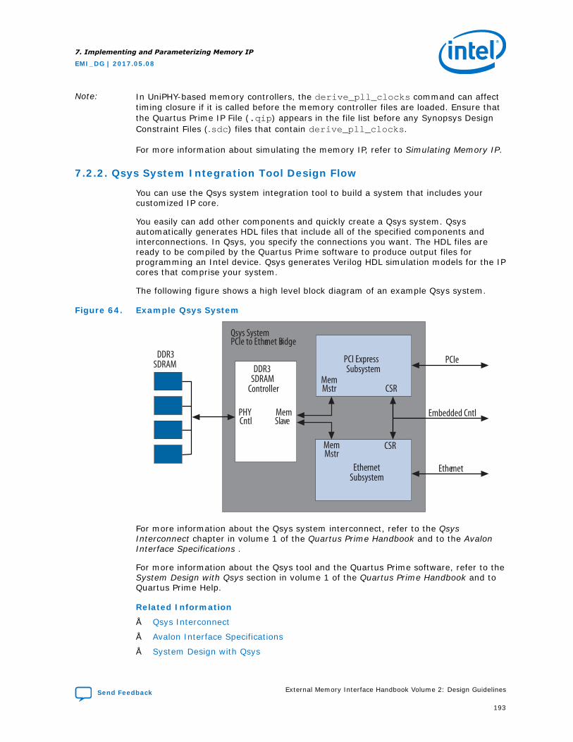
Note: In UniPHY-based memory controllers, the derive_pll_clocks command can affecttiming closure if it is called before the memory controller files are loaded. Ensure thatthe Quartus Prime IP File (.qip) appears in the file list before any Synopsys DesignConstraint Files (.sdc) files that contain derive_pll_clocks.
For more information about simulating the memory IP, refer to Simulating Memory IP.
7.2.2. Qsys System Integration Tool Design Flow
You can use the Qsys system integration tool to build a system that includes yourcustomized IP core.
You easily can add other components and quickly create a Qsys system. Qsysautomatically generates HDL files that include all of the specified components andinterconnections. In Qsys, you specify the connections you want. The HDL files areready to be compiled by the Quartus Prime software to produce output files forprogramming an Intel device. Qsys generates Verilog HDL simulation models for the IPcores that comprise your system.
The following figure shows a high level block diagram of an example Qsys system.
Figure 64. Example Qsys System
DDR3SDRAM
Ethernet Subsystem
Ethernet
Embedded Cntl
PCI ExpressSubsystem
Qsys SystemPCIe to Ethernet Bridge
PCIe
CSRMemMstr
MemSlave
PHYCntl
MemMstr
CSR
DDR3 SDRAM
Controller
For more information about the Qsys system interconnect, refer to the QsysInterconnect chapter in volume 1 of the Quartus Prime Handbook and to the AvalonInterface Specifications .
For more information about the Qsys tool and the Quartus Prime software, refer to theSystem Design with Qsys section in volume 1 of the Quartus Prime Handbook and toQuartus Prime Help.
Related Information
• Qsys Interconnect
• Avalon Interface Specifications
• System Design with Qsys
7. Implementing and Parameterizing Memory IP
EMI_DG | 2017.05.08
Send Feedback External Memory Interface Handbook Volume 2: Design Guidelines
193

7.2.2.1. Specify Parameters for the Qsys Flow
To specify parameters for your IP core using the Qsys flow, follow these steps:
1. In the Quartus Prime software, create a new Quartus Prime project using the NewProject Wizard available from the File menu.
2. On the Tools menu, click Qsys.
Note: Qsys automatically sets device parameters based on your Quartus Primeproject settings. To set device parameters manually, use the Device Familytab.
3. In the IP Catalog, select the available external memory interface IP from theMemory Interfaces and Controllers folder in the Library list. (For Arria 10EMIF for HPS, select the external memory interface IP from the Hard ProcessorComponents folder.) The relevant parameter editor appears.
Note: The availability of external memory interface IP depends on the devicefamily your design is using. To use Arria 10 External Memory Interface forHPS IP, your design must target a device containing at least one HPS CPUcore.
4. From the Presets list, select the preset matching your design requirement, andclick Apply.
Tip: If none of the presets match your design requirements, you can apply theclosest preset available and then change the inappropriate parametersmanually. This method may be faster than entering all the parametersmanually, and reduces the chance of having incorrect settings.
5. Specify the parameters on all tabs.
Note: • For detailed explanation of the parameters, refer to ParameterizingMemory Controllers with UniPHY IP and Parameterizing MemoryControllers with Arria 10 External Memory Interface IP.
• Although you have applied presets, you may need to modify some of thepreset parameters depending on the frequency of operation. A typicallist of parameters which you might need to change includes the MemoryCAS Latency setting, the Memory CAS Write Latency setting, and thetWTR, tFAW, tRRD, and tRTP settings.
• For UniPHY-based IP, turn on Generate power-of-2 bus widths forQsys or SOPC Builder on the Controller Settings tab.
Tip: • As a good practice, review any warning messages displayed in theMessages Window and correct any errors before making furtherchanges.
• To simplify future work, you might want to store the current configurationby saving your own presets. To create, modify, or remove your owncustom presets, click New, Update, or Delete at the bottom of thePresets list.
• If you want to generate an example design for your current configuration,click Example Design at the top-right corner of the parameter editor,specify a path for the example design, and click Ok.
6. Click Finish to complete the external memory interface IP instance and add it tothe system.
Note: The Finish button may be unavailable until you have corrected allparameterization errors listed in the Messages window.
7. Implementing and Parameterizing Memory IP
EMI_DG | 2017.05.08
External Memory Interface Handbook Volume 2: Design Guidelines Send Feedback
194
7.2.2.2. Completing the Qsys System
To complete the Qsys system, follow these steps:
1. Add and parameterize any additional components.
2. Connect the components using the Connection panel on the System Contentstab.
3. In the Export column, enter the name of any connections that should be a top-level Qsys system port.
Note: Ensure that the memory and oct interfaces are exported to the top-levelQsys system port. If these interfaces are already exported, take care not toaccidentally rename or delete either of them in the Export column of theSystem Contents tab.
4. Click Finish.
5. Specify the File Name and click Save.
6. When you are prompted to generate now, click Yes.
7. Set Create HDL design files for synthesis to either Verilog or VHDL.
Tip: If you want to do RTL simulation of your design, you should set Createsimulation model to either Verilog or VHDL. Some RTL simulation-relatedfiles, including simulator-specific scripts, are generated only if you specify thisparameter.
Note: For Arria 10 External Memory Interface IP, the synthesis and simulationmodel files are identical. However, there are some differences in file typeswhen generating for VHDL. For synthesis files, only the top-level wrapper isgenerated in VHDL; the other files are generated in System Verilog. Forsimulation files, all the files are generated as a Mentor-tagged encrypted IPfor VHDL-only simulator support.
8. Click Generate.
9. When generation has completed, click Finish.
10. If you are prompted to add the .qip file to the current Quartus Prime project,click Yes (If you want, you can turn on Automatically Add Quartus Prime IPFiles to all projects).
Tip: Always read the generated readme.txt file, because it contains informationand guidelines specific to your configuration.
You can now simulate and compile your design. But before compilation, you mustmake approrriate pin assignments. You can create a virtual pin to avoid makingspecific pin assignments for top-level signals during simulation and not yet ready tomap the design to hardware.
For information about the Quartus Prime software, including virtual pins and the IPCatalog and Qsys, refer to the Quartus Prime Help.
7.3. UniPHY-Based External Memory Interface IP
This section contains information about parameterizing UniPHY-based externalmemory interfaces.
7. Implementing and Parameterizing Memory IP
EMI_DG | 2017.05.08
Send Feedback External Memory Interface Handbook Volume 2: Design Guidelines
195
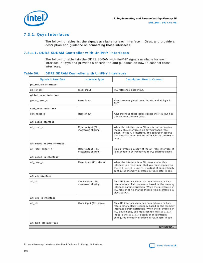
7.3.1. Qsys Interfaces
The following tables list the signals available for each interface in Qsys, and provide adescription and guidance on connecting those interfaces.
7.3.1.1. DDR2 SDRAM Controller with UniPHY Interfaces
The following table lists the DDR2 SDRAM with UniPHY signals available for eachinterface in Qsys and provides a description and guidance on how to connect thoseinterfaces.
Table 56. DDR2 SDRAM Controller with UniPHY Interfaces
Signals in Interface Interface Type Description/How to Connect
pll_ref_clk interface
pll_ref_clk Clock input PLL reference clock input.
global_reset interface
global_reset_n Reset input Asynchronous global reset for PLL and all logic inPHY.
soft_reset interface
soft_reset_n Reset input Asynchronous reset input. Resets the PHY, but notthe PLL that the PHY uses.
afi_reset interface
afi_reset_n Reset output (PLLmaster/no sharing)
When the interface is in PLL master or no sharingmodes, this interface is an asynchronous resetoutput of the AFI interface. The controller assertsthis interface when the PLL loses lock or the PHY isreset.
afi_reset_export interface
afi_reset_export_n Reset output (PLLmaster/no sharing)
This interface is a copy of the afi_reset interface. Itis intended to be connected to PLL sharing slaves.
afi_reset_in interface
afi_reset_n Reset input (PLL slave) When the interface is in PLL slave mode, thisinterface is a reset input that you must connect tothe afi_reset_export_n output of an identicallyconfigured memory interface in PLL master mode.
afi_clk interface
afi_clk Clock output (PLLmaster/no sharing)
This AFI interface clock can be a full-rate or half-rate memory clock frequency based on the memoryinterface parameterization. When the interface is inPLL master or no sharing modes, this interface is aclock output.
afi_clk_in interface
afi_clk Clock input (PLL slave) This AFI interface clock can be a full-rate or half-rate memory clock frequency based on the memoryinterface parameterization. When the interface is inPLL slave mode, you must connect this afi_clkinput to the afi_clk output of an identicallyconfigured memory interface in PLL master mode.
afi_half_clk interfacecontinued...
7. Implementing and Parameterizing Memory IP
EMI_DG | 2017.05.08
External Memory Interface Handbook Volume 2: Design Guidelines Send Feedback
196
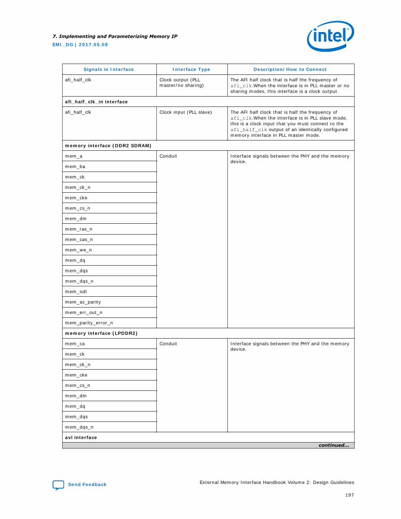
Signals in Interface Interface Type Description/How to Connect
afi_half_clk Clock output (PLLmaster/no sharing)
The AFI half clock that is half the frequency ofafi_clk.When the interface is in PLL master or nosharing modes, this interface is a clock output.
afi_half_clk_in interface
afi_half_clk Clock input (PLL slave) The AFI half clock that is half the frequency ofafi_clk.When the interface is in PLL slave mode,this is a clock input that you must connect to theafi_half_clk output of an identically configuredmemory interface in PLL master mode.
memory interface (DDR2 SDRAM)
mem_a Conduit Interface signals between the PHY and the memorydevice.
mem_ba
mem_ck
mem_ck_n
mem_cke
mem_cs_n
mem_dm
mem_ras_n
mem_cas_n
mem_we_n
mem_dq
mem_dqs
mem_dqs_n
mem_odt
mem_ac_parity
mem_err_out_n
mem_parity_error_n
memory interface (LPDDR2)
mem_ca Conduit Interface signals between the PHY and the memorydevice.
mem_ck
mem_ck_n
mem_cke
mem_cs_n
mem_dm
mem_dq
mem_dqs
mem_dqs_n
avl interfacecontinued...
7. Implementing and Parameterizing Memory IP
EMI_DG | 2017.05.08
Send Feedback External Memory Interface Handbook Volume 2: Design Guidelines
197
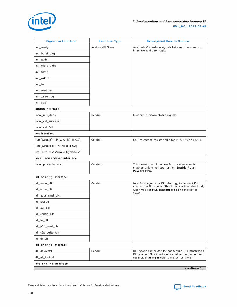
Signals in Interface Interface Type Description/How to Connect
avl_ready Avalon-MM Slave Avalon-MM interface signals between the memoryinterface and user logic.
avl_burst_begin
avl_addr
avl_rdata_valid
avl_rdata
avl_wdata
avl_be
avl_read_req
avl_write_req
avl_size
status interface
local_init_done Conduit Memory interface status signals.
local_cal_success
local_cal_fail
oct interface
rup (Stratix® III/IV, Arria® II GZ) Conduit OCT reference resistor pins for rup/rdn or rzqin.
rdn (Stratix III/IV, Arria II GZ)
rzq (Stratix V, Arria V, Cyclone V)
local_powerdown interface
local_powerdn_ack Conduit This powerdown interface for the controller isenabled only when you turn on Enable AutoPowerdown.
pll_sharing interface
pll_mem_clk Conduit Interface signals for PLL sharing, to connect PLLmasters to PLL slaves. This interface is enabled onlywhen you set PLL sharing mode to master orslave.
pll_write_clk
pll_addr_cmd_clk
pll_locked
pll_avl_clk
pll_config_clk
pll_hr_clk
pll_p2c_read_clk
pll_c2p_write_clk
pll_dr_clk
dll_sharing interface
dll_delayctrl Conduit DLL sharing interface for connecting DLL masters toDLL slaves. This interface is enabled only when youset DLL sharing mode to master or slave.dll_pll_locked
oct_sharing interfacecontinued...
7. Implementing and Parameterizing Memory IP
EMI_DG | 2017.05.08
External Memory Interface Handbook Volume 2: Design Guidelines Send Feedback
198
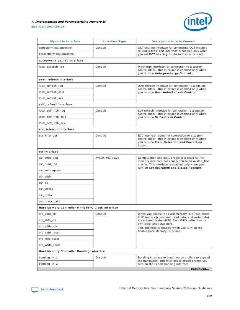
Signals in Interface Interface Type Description/How to Connect
seriesterminationcontrol Conduit OCT sharing interface for connecting OCT mastersto OCT slaves. This interface is enabled only whenyou set OCT sharing mode to master or slave.parallelterminationcontrol
autoprecharge_req interface
local_autopch_req Conduit Precharge interface for connection to a customcontrol block. This interface is enabled only whenyou turn on Auto precharge Control.
user_refresh interface
local_refresh_req Conduit User refresh interface for connection to a customcontrol block. This interface is enabled only whenyou turn on User Auto-Refresh Control.local_refresh_chip
local_refresh_ack
self_refresh interface
local_self_rfsh_req Conduit Self refresh interface for connection to a customcontrol block. This interface is enabled only whenyou turn on Self-refresh Control.local_self_rfsh_chip
local_self_rfsh_ack
ecc_interrupt interface
ecc_interrupt Conduit ECC interrupt signal for connection to a customcontrol block. This interface is enabled only whenyou turn on Error Detection and CorrectionLogic.
csr interface
csr_write_req Avalon-MM Slave Configuration and status register signals for thememory interface, for connection to an Avalon_MMmaster. This interface is enabled only when youturn on Configuration and Status Register.
csr_read_req
csr_waitrequest
csr_addr
csr_be
csr_wdata
csr_rdata
csr_rdata_valid
Hard Memory Controller MPFE FIFO Clock Interface
mp_cmd_clk Conduit When you enable the Hard Memory Interface, threeFIFO buffers (command, read data, and write data)are created in the MPFE. Each FIFO buffer has itsown clock and reset port.This interface is enabled when you turn on theEnable Hard Memory Interface.
mp_rfifo_clk
mp_wfifo_clk
mp_cmd_reset
mp_rfifo_reset
mp_wfifo_reset
Hard Memory Controller Bonding Interface
bonding_in_1 Conduit Bonding interface to bond two controllers to expandthe bandwidth. This interface is enabled when youturn on the Export bonding interface.bonding_in_2
continued...
7. Implementing and Parameterizing Memory IP
EMI_DG | 2017.05.08
Send Feedback External Memory Interface Handbook Volume 2: Design Guidelines
199
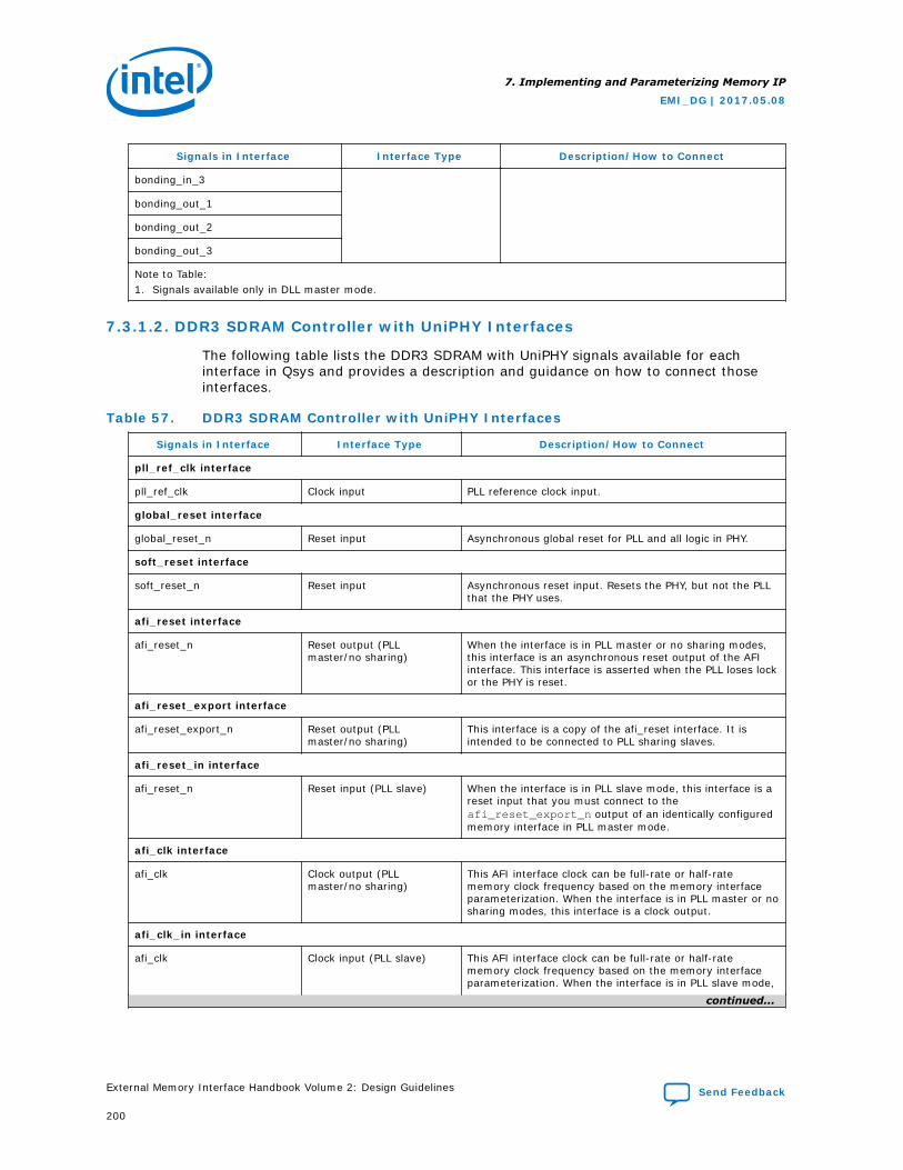
Signals in Interface Interface Type Description/How to Connect
bonding_in_3
bonding_out_1
bonding_out_2
bonding_out_3
Note to Table:1. Signals available only in DLL master mode.
7.3.1.2. DDR3 SDRAM Controller with UniPHY Interfaces
The following table lists the DDR3 SDRAM with UniPHY signals available for eachinterface in Qsys and provides a description and guidance on how to connect thoseinterfaces.
Table 57. DDR3 SDRAM Controller with UniPHY Interfaces
Signals in Interface Interface Type Description/How to Connect
pll_ref_clk interface
pll_ref_clk Clock input PLL reference clock input.
global_reset interface
global_reset_n Reset input Asynchronous global reset for PLL and all logic in PHY.
soft_reset interface
soft_reset_n Reset input Asynchronous reset input. Resets the PHY, but not the PLLthat the PHY uses.
afi_reset interface
afi_reset_n Reset output (PLLmaster/no sharing)
When the interface is in PLL master or no sharing modes,this interface is an asynchronous reset output of the AFIinterface. This interface is asserted when the PLL loses lockor the PHY is reset.
afi_reset_export interface
afi_reset_export_n Reset output (PLLmaster/no sharing)
This interface is a copy of the afi_reset interface. It isintended to be connected to PLL sharing slaves.
afi_reset_in interface
afi_reset_n Reset input (PLL slave) When the interface is in PLL slave mode, this interface is areset input that you must connect to theafi_reset_export_n output of an identically configuredmemory interface in PLL master mode.
afi_clk interface
afi_clk Clock output (PLLmaster/no sharing)
This AFI interface clock can be full-rate or half-ratememory clock frequency based on the memory interfaceparameterization. When the interface is in PLL master or nosharing modes, this interface is a clock output.
afi_clk_in interface
afi_clk Clock input (PLL slave) This AFI interface clock can be full-rate or half-ratememory clock frequency based on the memory interfaceparameterization. When the interface is in PLL slave mode,
continued...
7. Implementing and Parameterizing Memory IP
EMI_DG | 2017.05.08
External Memory Interface Handbook Volume 2: Design Guidelines Send Feedback
200
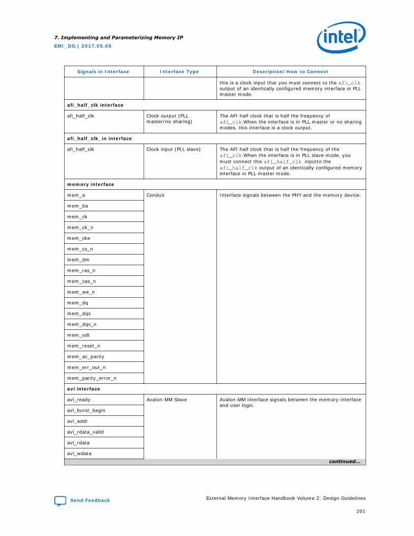
Signals in Interface Interface Type Description/How to Connect
this is a clock input that you must connect to the afi_clkoutput of an identically configured memory interface in PLLmaster mode.
afi_half_clk interface
afi_half_clk Clock output (PLLmaster/no sharing)
The AFI half clock that is half the frequency ofafi_clk.When the interface is in PLL master or no sharingmodes, this interface is a clock output.
afi_half_clk_in interface
afi_half_clk Clock input (PLL slave) The AFI half clock that is half the frequency of theafi_clk.When the interface is in PLL slave mode, youmust connect this afi_half_clk inputto theafi_half_clk output of an identically configured memoryinterface in PLL master mode.
memory interface
mem_a Conduit Interface signals between the PHY and the memory device.
mem_ba
mem_ck
mem_ck_n
mem_cke
mem_cs_n
mem_dm
mem_ras_n
mem_cas_n
mem_we_n
mem_dq
mem_dqs
mem_dqs_n
mem_odt
mem_reset_n
mem_ac_parity
mem_err_out_n
mem_parity_error_n
avl interface
avl_ready Avalon-MM Slave Avalon-MM interface signals between the memory interfaceand user logic.
avl_burst_begin
avl_addr
avl_rdata_valid
avl_rdata
avl_wdata
continued...
7. Implementing and Parameterizing Memory IP
EMI_DG | 2017.05.08
Send Feedback External Memory Interface Handbook Volume 2: Design Guidelines
201
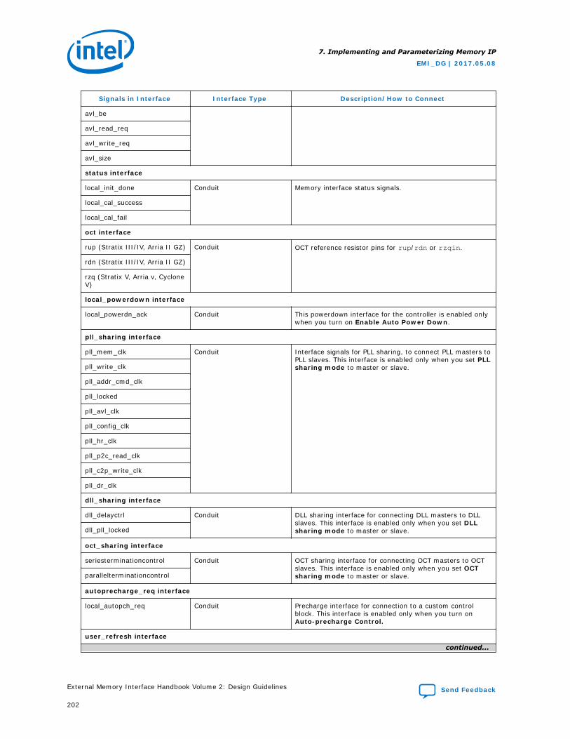
Signals in Interface Interface Type Description/How to Connect
avl_be
avl_read_req
avl_write_req
avl_size
status interface
local_init_done Conduit Memory interface status signals.
local_cal_success
local_cal_fail
oct interface
rup (Stratix III/IV, Arria II GZ) Conduit OCT reference resistor pins for rup/rdn or rzqin.
rdn (Stratix III/IV, Arria II GZ)
rzq (Stratix V, Arria v, CycloneV)
local_powerdown interface
local_powerdn_ack Conduit This powerdown interface for the controller is enabled onlywhen you turn on Enable Auto Power Down.
pll_sharing interface
pll_mem_clk Conduit Interface signals for PLL sharing, to connect PLL masters toPLL slaves. This interface is enabled only when you set PLLsharing mode to master or slave.pll_write_clk
pll_addr_cmd_clk
pll_locked
pll_avl_clk
pll_config_clk
pll_hr_clk
pll_p2c_read_clk
pll_c2p_write_clk
pll_dr_clk
dll_sharing interface
dll_delayctrl Conduit DLL sharing interface for connecting DLL masters to DLLslaves. This interface is enabled only when you set DLLsharing mode to master or slave.dll_pll_locked
oct_sharing interface
seriesterminationcontrol Conduit OCT sharing interface for connecting OCT masters to OCTslaves. This interface is enabled only when you set OCTsharing mode to master or slave.parallelterminationcontrol
autoprecharge_req interface
local_autopch_req Conduit Precharge interface for connection to a custom controlblock. This interface is enabled only when you turn onAuto-precharge Control.
user_refresh interfacecontinued...
7. Implementing and Parameterizing Memory IP
EMI_DG | 2017.05.08
External Memory Interface Handbook Volume 2: Design Guidelines Send Feedback
202
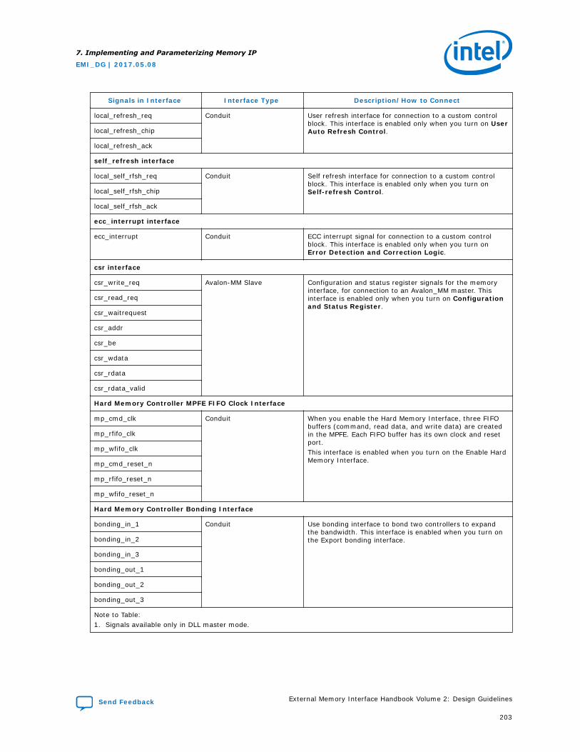
Signals in Interface Interface Type Description/How to Connect
local_refresh_req Conduit User refresh interface for connection to a custom controlblock. This interface is enabled only when you turn on UserAuto Refresh Control.local_refresh_chip
local_refresh_ack
self_refresh interface
local_self_rfsh_req Conduit Self refresh interface for connection to a custom controlblock. This interface is enabled only when you turn onSelf-refresh Control.local_self_rfsh_chip
local_self_rfsh_ack
ecc_interrupt interface
ecc_interrupt Conduit ECC interrupt signal for connection to a custom controlblock. This interface is enabled only when you turn onError Detection and Correction Logic.
csr interface
csr_write_req Avalon-MM Slave Configuration and status register signals for the memoryinterface, for connection to an Avalon_MM master. Thisinterface is enabled only when you turn on Configurationand Status Register.
csr_read_req
csr_waitrequest
csr_addr
csr_be
csr_wdata
csr_rdata
csr_rdata_valid
Hard Memory Controller MPFE FIFO Clock Interface
mp_cmd_clk Conduit When you enable the Hard Memory Interface, three FIFObuffers (command, read data, and write data) are createdin the MPFE. Each FIFO buffer has its own clock and resetport.This interface is enabled when you turn on the Enable HardMemory Interface.
mp_rfifo_clk
mp_wfifo_clk
mp_cmd_reset_n
mp_rfifo_reset_n
mp_wfifo_reset_n
Hard Memory Controller Bonding Interface
bonding_in_1 Conduit Use bonding interface to bond two controllers to expandthe bandwidth. This interface is enabled when you turn onthe Export bonding interface.bonding_in_2
bonding_in_3
bonding_out_1
bonding_out_2
bonding_out_3
Note to Table:1. Signals available only in DLL master mode.
7. Implementing and Parameterizing Memory IP
EMI_DG | 2017.05.08
Send Feedback External Memory Interface Handbook Volume 2: Design Guidelines
203
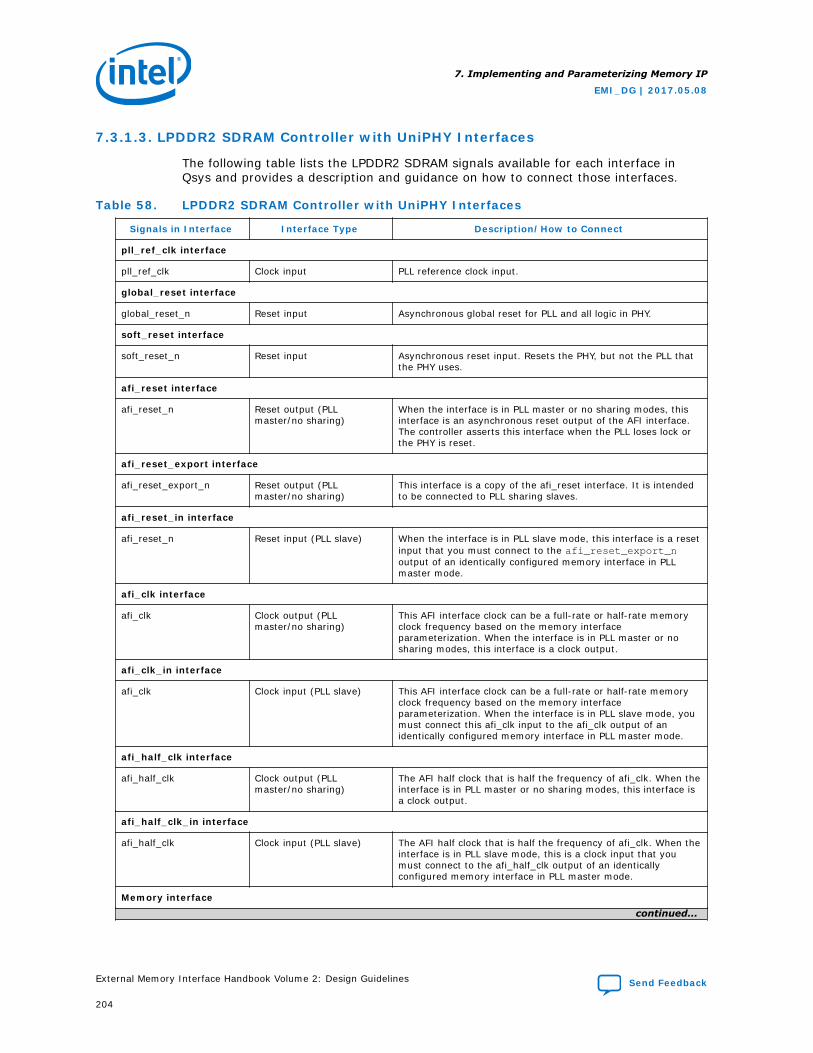
7.3.1.3. LPDDR2 SDRAM Controller with UniPHY Interfaces
The following table lists the LPDDR2 SDRAM signals available for each interface inQsys and provides a description and guidance on how to connect those interfaces.
Table 58. LPDDR2 SDRAM Controller with UniPHY Interfaces
Signals in Interface Interface Type Description/How to Connect
pll_ref_clk interface
pll_ref_clk Clock input PLL reference clock input.
global_reset interface
global_reset_n Reset input Asynchronous global reset for PLL and all logic in PHY.
soft_reset interface
soft_reset_n Reset input Asynchronous reset input. Resets the PHY, but not the PLL thatthe PHY uses.
afi_reset interface
afi_reset_n Reset output (PLLmaster/no sharing)
When the interface is in PLL master or no sharing modes, thisinterface is an asynchronous reset output of the AFI interface.The controller asserts this interface when the PLL loses lock orthe PHY is reset.
afi_reset_export interface
afi_reset_export_n Reset output (PLLmaster/no sharing)
This interface is a copy of the afi_reset interface. It is intendedto be connected to PLL sharing slaves.
afi_reset_in interface
afi_reset_n Reset input (PLL slave) When the interface is in PLL slave mode, this interface is a resetinput that you must connect to the afi_reset_export_noutput of an identically configured memory interface in PLLmaster mode.
afi_clk interface
afi_clk Clock output (PLLmaster/no sharing)
This AFI interface clock can be a full-rate or half-rate memoryclock frequency based on the memory interfaceparameterization. When the interface is in PLL master or nosharing modes, this interface is a clock output.
afi_clk_in interface
afi_clk Clock input (PLL slave) This AFI interface clock can be a full-rate or half-rate memoryclock frequency based on the memory interfaceparameterization. When the interface is in PLL slave mode, youmust connect this afi_clk input to the afi_clk output of anidentically configured memory interface in PLL master mode.
afi_half_clk interface
afi_half_clk Clock output (PLLmaster/no sharing)
The AFI half clock that is half the frequency of afi_clk. When theinterface is in PLL master or no sharing modes, this interface isa clock output.
afi_half_clk_in interface
afi_half_clk Clock input (PLL slave) The AFI half clock that is half the frequency of afi_clk. When theinterface is in PLL slave mode, this is a clock input that youmust connect to the afi_half_clk output of an identicallyconfigured memory interface in PLL master mode.
Memory interfacecontinued...
7. Implementing and Parameterizing Memory IP
EMI_DG | 2017.05.08
External Memory Interface Handbook Volume 2: Design Guidelines Send Feedback
204
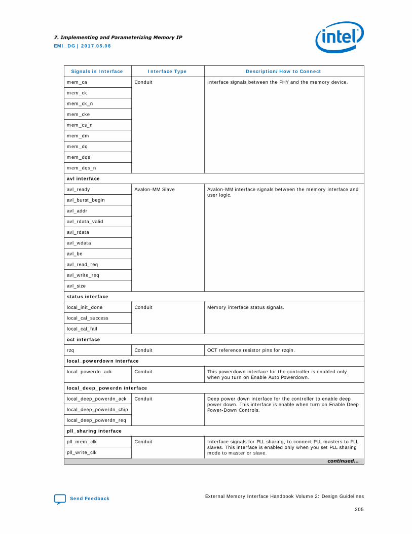
Signals in Interface Interface Type Description/How to Connect
mem_ca Conduit Interface signals between the PHY and the memory device.
mem_ck
mem_ck_n
mem_cke
mem_cs_n
mem_dm
mem_dq
mem_dqs
mem_dqs_n
avl interface
avl_ready Avalon-MM Slave Avalon-MM interface signals between the memory interface anduser logic.
avl_burst_begin
avl_addr
avl_rdata_valid
avl_rdata
avl_wdata
avl_be
avl_read_req
avl_write_req
avl_size
status interface
local_init_done Conduit Memory interface status signals.
local_cal_success
local_cal_fail
oct interface
rzq Conduit OCT reference resistor pins for rzqin.
local_powerdown interface
local_powerdn_ack Conduit This powerdown interface for the controller is enabled onlywhen you turn on Enable Auto Powerdown.
local_deep_powerdn interface
local_deep_powerdn_ack Conduit Deep power down interface for the controller to enable deeppower down. This interface is enable when turn on Enable DeepPower-Down Controls.local_deep_powerdn_chip
local_deep_powerdn_req
pll_sharing interface
pll_mem_clk Conduit Interface signals for PLL sharing, to connect PLL masters to PLLslaves. This interface is enabled only when you set PLL sharingmode to master or slave.pll_write_clk
continued...
7. Implementing and Parameterizing Memory IP
EMI_DG | 2017.05.08
Send Feedback External Memory Interface Handbook Volume 2: Design Guidelines
205
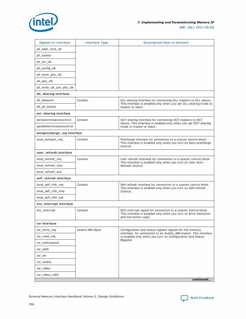
Signals in Interface Interface Type Description/How to Connect
pll_addr_cmd_clk
pll_locked
pll_avl_clk
pll_config_clk
pll_mem_phy_clk
afi_phy_clk
pll_write_clk_pre_phy_clk
dll_sharing interface
dll_delayctrl Conduit DLL sharing interface for connecting DLL masters to DLL slaves.This interface is enabled only when you set DLL sharing mode tomaster or slave.dll_pll_locked
oct_sharing interface
seriesterminationcontrol Conduit OCT sharing interface for connecting OCT masters to OCTslaves. This interface is enabled only when you set OCT sharingmode to master or slave.parallelterminationcontrol
autoprecharge_req interface
local_autopch_req Conduit Precharge interface for connection to a custom control block.This interface is enabled only when you turn on Auto-prechargeControl.
user_refresh interface
local_refresh_req Conduit User refresh interface for connection to a custom control block.This interface is enabled only when you turn on User Auto-Refresh Control.local_refresh_chip
local_refresh_ack
self_refresh interface
local_self_rfsh_req Conduit Self refresh interface for connection to a custom control block.This interface is enabled only when you turn on Self-refreshControl.local_self_rfsh_chip
local_self_rfsh_ack
ecc_interrupt interface
ecc_interrupt Conduit ECC interrupt signal for connection to a custom control block.This interface is enabled only when you turn on Error Detectionand Correction Logic.
csr interface
csr_write_req Avalon-MM Slave Configuration and status register signals for the memoryinterface, for connection to an Avalon_MM master. This interfaceis enabled only when you turn on Configuration and StatusRegister.
csr_read_req
csr_waitrequest
csr_addr
csr_be
csr_wdata
csr_rdata
csr_rdata_valid
continued...
7. Implementing and Parameterizing Memory IP
EMI_DG | 2017.05.08
External Memory Interface Handbook Volume 2: Design Guidelines Send Feedback
206
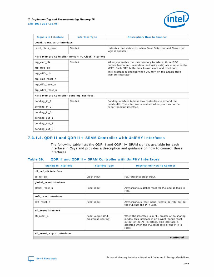
Signals in Interface Interface Type Description/How to Connect
Local_rdata_error interface
Local_rdata_error Conduit Indicates read data error when Error Detection and Correctionlogic is enabled.
Hard Memory Controller MPFE FIFO Clock Interface
mp_cmd_clk Conduit When you enable the Hard Memory Interface, three FIFObuffers (command, read data, and write data) are created in theMPFE. Each FIFO buffer has its own clock and reset port.This interface is enabled when you turn on the Enable HardMemory Interface.
mp_rfifo_clk
mp_wfifo_clk
mp_cmd_reset_n
mp_rfifo_reset_n
mp_wfifo_reset_n
Hard Memory Controller Bonding Interface
bonding_in_1 Conduit Bonding interface to bond two controllers to expand thebandwidth. This interface is enabled when you turn on theExport bonding interface.bonding_in_2
bonding_in_3
bonding_out_1
bonding_out_2
bonding_out_3
7.3.1.4. QDR II and QDR II+ SRAM Controller with UniPHY Interfaces
The following table lists the QDR II and QDR II+ SRAM signals available for eachinterface in Qsys and provides a description and guidance on how to connect thoseinterfaces.
Table 59. QDR II and QDR II+ SRAM Controller with UniPHY Interfaces
Signals in Interface Interface Type Description/How to Connect
pll_ref_clk interface
pll_ref_clk Clock input PLL reference clock input.
global_reset interface
global_reset_n Reset input Asynchronous global reset for PLL and all logic inPHY.
soft_reset interface
soft_reset_n Reset input Asynchronous reset input. Resets the PHY, but notthe PLL that the PHY uses.
afi_reset interface
afi_reset_n Reset output (PLLmaster/no sharing)
When the interface is in PLL master or no sharingmodes, this interface is an asynchronous resetoutput of the AFI interface. This interface isasserted when the PLL loses lock or the PHY isreset.
afi_reset_export interfacecontinued...
7. Implementing and Parameterizing Memory IP
EMI_DG | 2017.05.08
Send Feedback External Memory Interface Handbook Volume 2: Design Guidelines
207
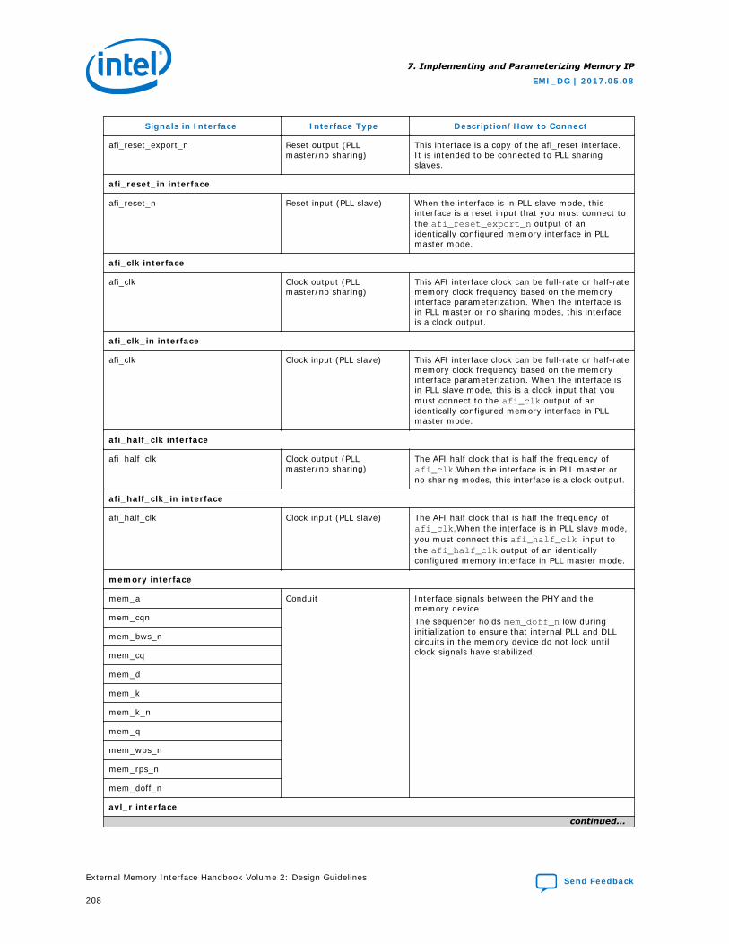
Signals in Interface Interface Type Description/How to Connect
afi_reset_export_n Reset output (PLLmaster/no sharing)
This interface is a copy of the afi_reset interface.It is intended to be connected to PLL sharingslaves.
afi_reset_in interface
afi_reset_n Reset input (PLL slave) When the interface is in PLL slave mode, thisinterface is a reset input that you must connect tothe afi_reset_export_n output of anidentically configured memory interface in PLLmaster mode.
afi_clk interface
afi_clk Clock output (PLLmaster/no sharing)
This AFI interface clock can be full-rate or half-ratememory clock frequency based on the memoryinterface parameterization. When the interface isin PLL master or no sharing modes, this interfaceis a clock output.
afi_clk_in interface
afi_clk Clock input (PLL slave) This AFI interface clock can be full-rate or half-ratememory clock frequency based on the memoryinterface parameterization. When the interface isin PLL slave mode, this is a clock input that youmust connect to the afi_clk output of anidentically configured memory interface in PLLmaster mode.
afi_half_clk interface
afi_half_clk Clock output (PLLmaster/no sharing)
The AFI half clock that is half the frequency ofafi_clk.When the interface is in PLL master orno sharing modes, this interface is a clock output.
afi_half_clk_in interface
afi_half_clk Clock input (PLL slave) The AFI half clock that is half the frequency ofafi_clk.When the interface is in PLL slave mode,you must connect this afi_half_clk input tothe afi_half_clk output of an identicallyconfigured memory interface in PLL master mode.
memory interface
mem_a Conduit Interface signals between the PHY and thememory device.The sequencer holds mem_doff_n low duringinitialization to ensure that internal PLL and DLLcircuits in the memory device do not lock untilclock signals have stabilized.
mem_cqn
mem_bws_n
mem_cq
mem_d
mem_k
mem_k_n
mem_q
mem_wps_n
mem_rps_n
mem_doff_n
avl_r interfacecontinued...
7. Implementing and Parameterizing Memory IP
EMI_DG | 2017.05.08
External Memory Interface Handbook Volume 2: Design Guidelines Send Feedback
208
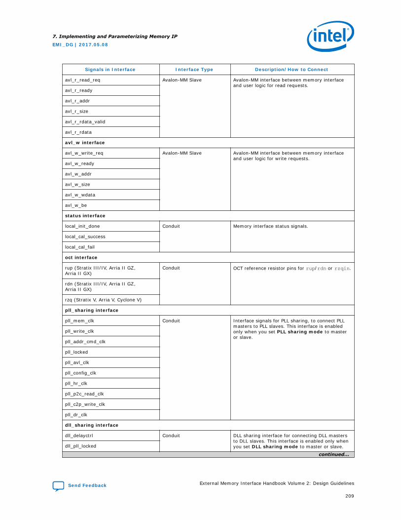
Signals in Interface Interface Type Description/How to Connect
avl_r_read_req Avalon-MM Slave Avalon-MM interface between memory interfaceand user logic for read requests.
avl_r_ready
avl_r_addr
avl_r_size
avl_r_rdata_valid
avl_r_rdata
avl_w interface
avl_w_write_req Avalon-MM Slave Avalon-MM interface between memory interfaceand user logic for write requests.
avl_w_ready
avl_w_addr
avl_w_size
avl_w_wdata
avl_w_be
status interface
local_init_done Conduit Memory interface status signals.
local_cal_success
local_cal_fail
oct interface
rup (Stratix III/IV, Arria II GZ,Arria II GX)
Conduit OCT reference resistor pins for rup/rdn or rzqin.
rdn (Stratix III/IV, Arria II GZ,Arria II GX)
rzq (Stratix V, Arria V, Cyclone V)
pll_sharing interface
pll_mem_clk Conduit Interface signals for PLL sharing, to connect PLLmasters to PLL slaves. This interface is enabledonly when you set PLL sharing mode to masteror slave.
pll_write_clk
pll_addr_cmd_clk
pll_locked
pll_avl_clk
pll_config_clk
pll_hr_clk
pll_p2c_read_clk
pll_c2p_write_clk
pll_dr_clk
dll_sharing interface
dll_delayctrl Conduit DLL sharing interface for connecting DLL mastersto DLL slaves. This interface is enabled only whenyou set DLL sharing mode to master or slave.dll_pll_locked
continued...
7. Implementing and Parameterizing Memory IP
EMI_DG | 2017.05.08
Send Feedback External Memory Interface Handbook Volume 2: Design Guidelines
209
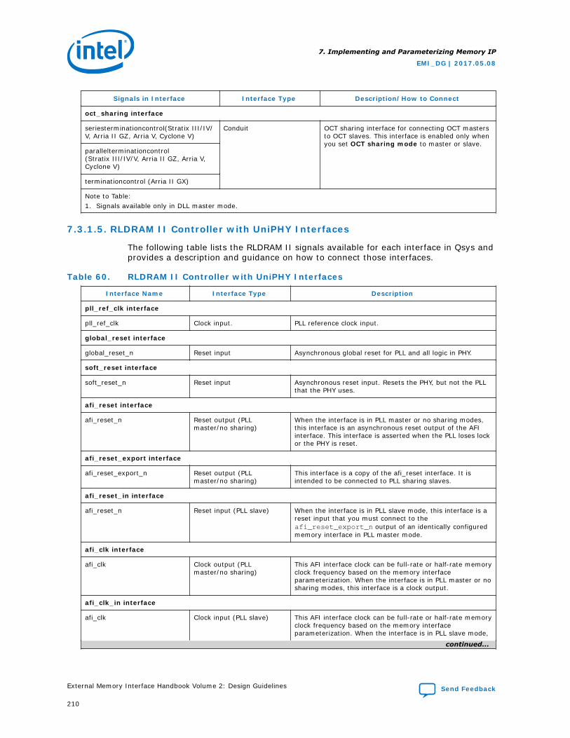
Signals in Interface Interface Type Description/How to Connect
oct_sharing interface
seriesterminationcontrol(Stratix III/IV/V, Arria II GZ, Arria V, Cyclone V)
Conduit OCT sharing interface for connecting OCT mastersto OCT slaves. This interface is enabled only whenyou set OCT sharing mode to master or slave.
parallelterminationcontrol(Stratix III/IV/V, Arria II GZ, Arria V,Cyclone V)
terminationcontrol (Arria II GX)
Note to Table:1. Signals available only in DLL master mode.
7.3.1.5. RLDRAM II Controller with UniPHY Interfaces
The following table lists the RLDRAM II signals available for each interface in Qsys andprovides a description and guidance on how to connect those interfaces.
Table 60. RLDRAM II Controller with UniPHY Interfaces
Interface Name Interface Type Description
pll_ref_clk interface
pll_ref_clk Clock input. PLL reference clock input.
global_reset interface
global_reset_n Reset input Asynchronous global reset for PLL and all logic in PHY.
soft_reset interface
soft_reset_n Reset input Asynchronous reset input. Resets the PHY, but not the PLLthat the PHY uses.
afi_reset interface
afi_reset_n Reset output (PLLmaster/no sharing)
When the interface is in PLL master or no sharing modes,this interface is an asynchronous reset output of the AFIinterface. This interface is asserted when the PLL loses lockor the PHY is reset.
afi_reset_export interface
afi_reset_export_n Reset output (PLLmaster/no sharing)
This interface is a copy of the afi_reset interface. It isintended to be connected to PLL sharing slaves.
afi_reset_in interface
afi_reset_n Reset input (PLL slave) When the interface is in PLL slave mode, this interface is areset input that you must connect to theafi_reset_export_n output of an identically configuredmemory interface in PLL master mode.
afi_clk interface
afi_clk Clock output (PLLmaster/no sharing)
This AFI interface clock can be full-rate or half-rate memoryclock frequency based on the memory interfaceparameterization. When the interface is in PLL master or nosharing modes, this interface is a clock output.
afi_clk_in interface
afi_clk Clock input (PLL slave) This AFI interface clock can be full-rate or half-rate memoryclock frequency based on the memory interfaceparameterization. When the interface is in PLL slave mode,
continued...
7. Implementing and Parameterizing Memory IP
EMI_DG | 2017.05.08
External Memory Interface Handbook Volume 2: Design Guidelines Send Feedback
210
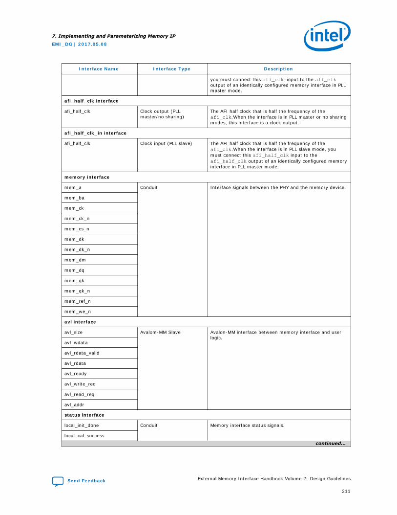
Interface Name Interface Type Description
you must connect this afi_clk input to the afi_clkoutput of an identically configured memory interface in PLLmaster mode.
afi_half_clk interface
afi_half_clk Clock output (PLLmaster/no sharing)
The AFI half clock that is half the frequency of theafi_clk.When the interface is in PLL master or no sharingmodes, this interface is a clock output.
afi_half_clk_in interface
afi_half_clk Clock input (PLL slave) The AFI half clock that is half the frequency of theafi_clk.When the interface is in PLL slave mode, youmust connect this afi_half_clk input to theafi_half_clk output of an identically configured memoryinterface in PLL master mode.
memory interface
mem_a Conduit Interface signals between the PHY and the memory device.
mem_ba
mem_ck
mem_ck_n
mem_cs_n
mem_dk
mem_dk_n
mem_dm
mem_dq
mem_qk
mem_qk_n
mem_ref_n
mem_we_n
avl interface
avl_size Avalom-MM Slave Avalon-MM interface between memory interface and userlogic.
avl_wdata
avl_rdata_valid
avl_rdata
avl_ready
avl_write_req
avl_read_req
avl_addr
status interface
local_init_done Conduit Memory interface status signals.
local_cal_success
continued...
7. Implementing and Parameterizing Memory IP
EMI_DG | 2017.05.08
Send Feedback External Memory Interface Handbook Volume 2: Design Guidelines
211
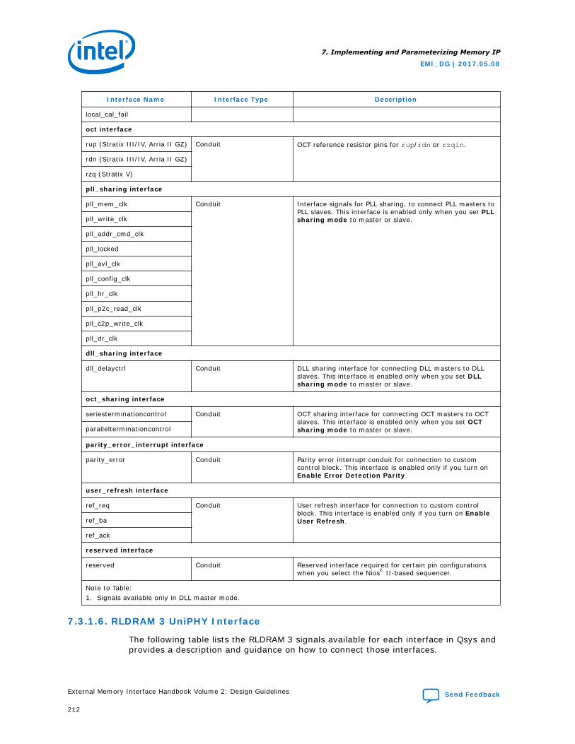
Interface Name Interface Type Description
local_cal_fail
oct interface
rup (Stratix III/IV, Arria II GZ) Conduit OCT reference resistor pins for rup/rdn or rzqin.
rdn (Stratix III/IV, Arria II GZ)
rzq (Stratix V)
pll_sharing interface
pll_mem_clk Conduit Interface signals for PLL sharing, to connect PLL masters toPLL slaves. This interface is enabled only when you set PLLsharing mode to master or slave.pll_write_clk
pll_addr_cmd_clk
pll_locked
pll_avl_clk
pll_config_clk
pll_hr_clk
pll_p2c_read_clk
pll_c2p_write_clk
pll_dr_clk
dll_sharing interface
dll_delayctrl Conduit DLL sharing interface for connecting DLL masters to DLLslaves. This interface is enabled only when you set DLLsharing mode to master or slave.
oct_sharing interface
seriesterminationcontrol Conduit OCT sharing interface for connecting OCT masters to OCTslaves. This interface is enabled only when you set OCTsharing mode to master or slave.parallelterminationcontrol
parity_error_interrupt interface
parity_error Conduit Parity error interrupt conduit for connection to customcontrol block. This interface is enabled only if you turn onEnable Error Detection Parity.
user_refresh interface
ref_req Conduit User refresh interface for connection to custom controlblock. This interface is enabled only if you turn on EnableUser Refresh.ref_ba
ref_ack
reserved interface
reserved Conduit Reserved interface required for certain pin configurationswhen you select the Nios® II-based sequencer.
Note to Table:1. Signals available only in DLL master mode.
7.3.1.6. RLDRAM 3 UniPHY Interface
The following table lists the RLDRAM 3 signals available for each interface in Qsys andprovides a description and guidance on how to connect those interfaces.
7. Implementing and Parameterizing Memory IP
EMI_DG | 2017.05.08
External Memory Interface Handbook Volume 2: Design Guidelines Send Feedback
212
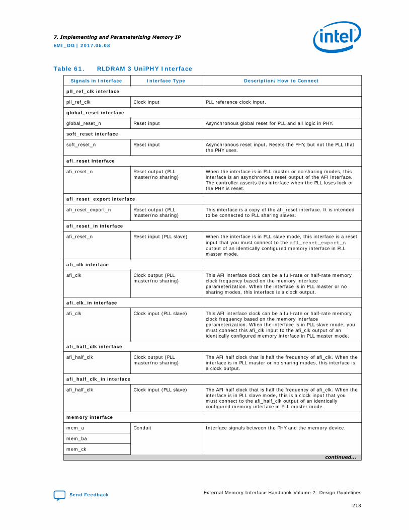
Table 61. RLDRAM 3 UniPHY Interface
Signals in Interface Interface Type Description/How to Connect
pll_ref_clk interface
pll_ref_clk Clock input PLL reference clock input.
global_reset interface
global_reset_n Reset input Asynchronous global reset for PLL and all logic in PHY.
soft_reset interface
soft_reset_n Reset input Asynchronous reset input. Resets the PHY, but not the PLL thatthe PHY uses.
afi_reset interface
afi_reset_n Reset output (PLLmaster/no sharing)
When the interface is in PLL master or no sharing modes, thisinterface is an asynchronous reset output of the AFI interface.The controller asserts this interface when the PLL loses lock orthe PHY is reset.
afi_reset_export interface
afi_reset_export_n Reset output (PLLmaster/no sharing)
This interface is a copy of the afi_reset interface. It is intendedto be connected to PLL sharing slaves.
afi_reset_in interface
afi_reset_n Reset input (PLL slave) When the interface is in PLL slave mode, this interface is a resetinput that you must connect to the afi_reset_export_noutput of an identically configured memory interface in PLLmaster mode.
afi_clk interface
afi_clk Clock output (PLLmaster/no sharing)
This AFI interface clock can be a full-rate or half-rate memoryclock frequency based on the memory interfaceparameterization. When the interface is in PLL master or nosharing modes, this interface is a clock output.
afi_clk_in interface
afi_clk Clock input (PLL slave) This AFI interface clock can be a full-rate or half-rate memoryclock frequency based on the memory interfaceparameterization. When the interface is in PLL slave mode, youmust connect this afi_clk input to the afi_clk output of anidentically configured memory interface in PLL master mode.
afi_half_clk interface
afi_half_clk Clock output (PLLmaster/no sharing)
The AFI half clock that is half the frequency of afi_clk. When theinterface is in PLL master or no sharing modes, this interface isa clock output.
afi_half_clk_in interface
afi_half_clk Clock input (PLL slave) The AFI half clock that is half the frequency of afi_clk. When theinterface is in PLL slave mode, this is a clock input that youmust connect to the afi_half_clk output of an identicallyconfigured memory interface in PLL master mode.
memory interface
mem_a Conduit Interface signals between the PHY and the memory device.
mem_ba
mem_ck
continued...
7. Implementing and Parameterizing Memory IP
EMI_DG | 2017.05.08
Send Feedback External Memory Interface Handbook Volume 2: Design Guidelines
213
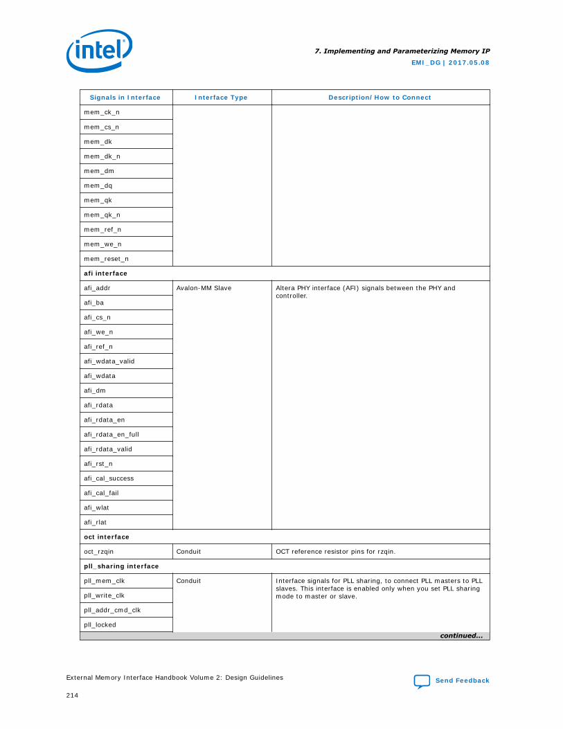
Signals in Interface Interface Type Description/How to Connect
mem_ck_n
mem_cs_n
mem_dk
mem_dk_n
mem_dm
mem_dq
mem_qk
mem_qk_n
mem_ref_n
mem_we_n
mem_reset_n
afi interface
afi_addr Avalon-MM Slave Altera PHY interface (AFI) signals between the PHY andcontroller.
afi_ba
afi_cs_n
afi_we_n
afi_ref_n
afi_wdata_valid
afi_wdata
afi_dm
afi_rdata
afi_rdata_en
afi_rdata_en_full
afi_rdata_valid
afi_rst_n
afi_cal_success
afi_cal_fail
afi_wlat
afi_rlat
oct interface
oct_rzqin Conduit OCT reference resistor pins for rzqin.
pll_sharing interface
pll_mem_clk Conduit Interface signals for PLL sharing, to connect PLL masters to PLLslaves. This interface is enabled only when you set PLL sharingmode to master or slave.pll_write_clk
pll_addr_cmd_clk
pll_locked
continued...
7. Implementing and Parameterizing Memory IP
EMI_DG | 2017.05.08
External Memory Interface Handbook Volume 2: Design Guidelines Send Feedback
214
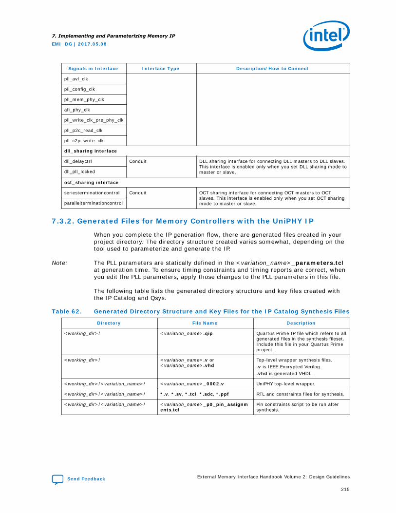
Signals in Interface Interface Type Description/How to Connect
pll_avl_clk
pll_config_clk
pll_mem_phy_clk
afi_phy_clk
pll_write_clk_pre_phy_clk
pll_p2c_read_clk
pll_c2p_write_clk
dll_sharing interface
dll_delayctrl Conduit DLL sharing interface for connecting DLL masters to DLL slaves.This interface is enabled only when you set DLL sharing mode tomaster or slave.dll_pll_locked
oct_sharing interface
seriesterminationcontrol Conduit OCT sharing interface for connecting OCT masters to OCTslaves. This interface is enabled only when you set OCT sharingmode to master or slave.parallelterminationcontrol
7.3.2. Generated Files for Memory Controllers with the UniPHY IP
When you complete the IP generation flow, there are generated files created in yourproject directory. The directory structure created varies somewhat, depending on thetool used to parameterize and generate the IP.
Note: The PLL parameters are statically defined in the <variation_name>_parameters.tclat generation time. To ensure timing constraints and timing reports are correct, whenyou edit the PLL parameters, apply those changes to the PLL parameters in this file.
The following table lists the generated directory structure and key files created withthe IP Catalog and Qsys.
Table 62. Generated Directory Structure and Key Files for the IP Catalog Synthesis Files
Directory File Name Description
<working_dir>/ <variation_name>.qip Quartus Prime IP file which refers to allgenerated files in the synthesis fileset.Include this file in your Quartus Primeproject.
<working_dir>/ <variation_name>.v or<variation_name>.vhd
Top-level wrapper synthesis files..v is IEEE Encrypted Verilog..vhd is generated VHDL.
<working_dir>/<variation_name>/ <variation_name>_0002.v UniPHY top-level wrapper.
<working_dir>/<variation_name>/ *.v, *.sv, *.tcl, *.sdc, *.ppf RTL and constraints files for synthesis.
<working_dir>/<variation_name>/ <variation_name>_p0_pin_assignments.tcl
Pin constraints script to be run aftersynthesis.
7. Implementing and Parameterizing Memory IP
EMI_DG | 2017.05.08
Send Feedback External Memory Interface Handbook Volume 2: Design Guidelines
215
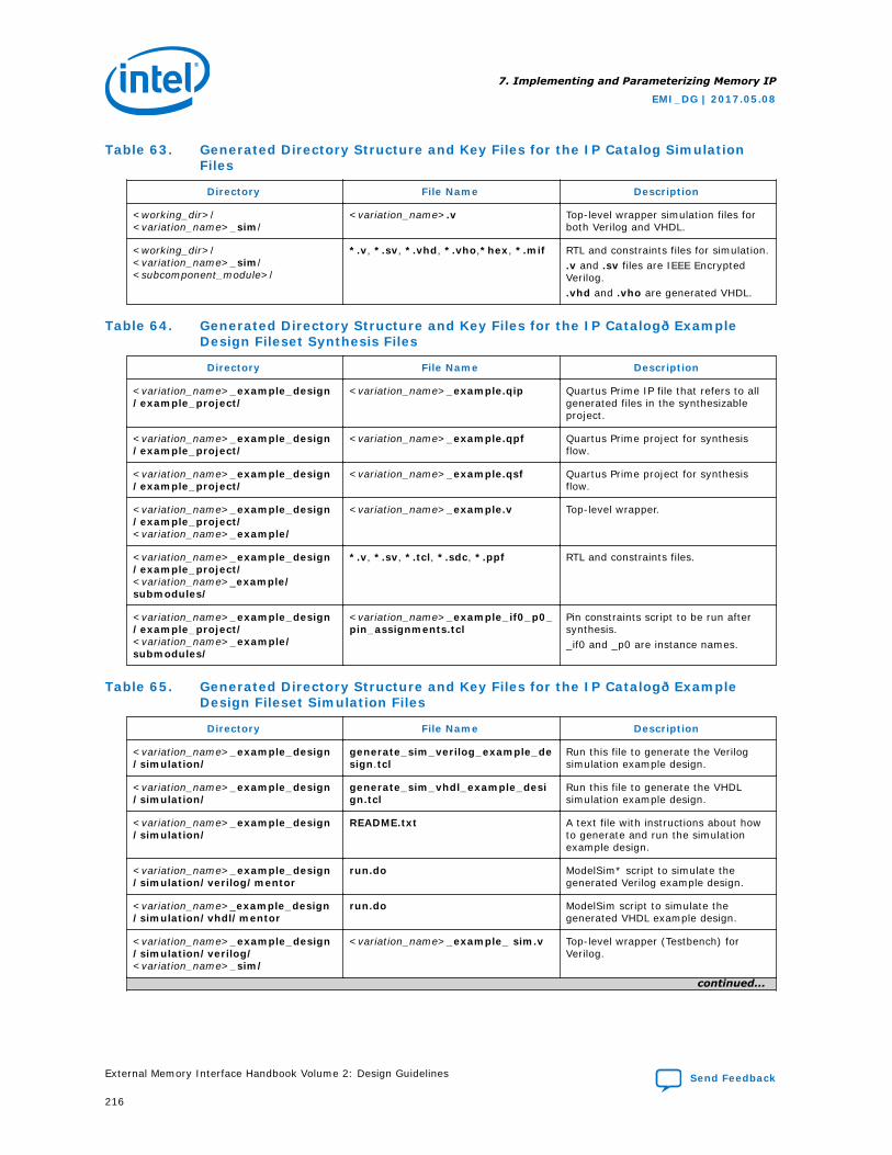
Table 63. Generated Directory Structure and Key Files for the IP Catalog SimulationFiles
Directory File Name Description
<working_dir>/<variation_name>_sim/
<variation_name>.v Top-level wrapper simulation files forboth Verilog and VHDL.
<working_dir>/<variation_name>_sim/<subcomponent_module>/
*.v, *.sv, *.vhd, *.vho,*hex, *.mif RTL and constraints files for simulation..v and .sv files are IEEE EncryptedVerilog..vhd and .vho are generated VHDL.
Table 64. Generated Directory Structure and Key Files for the IP Catalog—ExampleDesign Fileset Synthesis Files
Directory File Name Description
<variation_name>_example_design/example_project/
<variation_name>_example.qip Quartus Prime IP file that refers to allgenerated files in the synthesizableproject.
<variation_name>_example_design/example_project/
<variation_name>_example.qpf Quartus Prime project for synthesisflow.
<variation_name>_example_design/example_project/
<variation_name>_example.qsf Quartus Prime project for synthesisflow.
<variation_name>_example_design/example_project/ <variation_name>_example/
<variation_name>_example.v Top-level wrapper.
<variation_name>_example_design/example_project/ <variation_name>_example/submodules/
*.v, *.sv, *.tcl, *.sdc, *.ppf RTL and constraints files.
<variation_name>_example_design/example_project/ <variation_name>_example/submodules/
<variation_name>_example_if0_p0_pin_assignments.tcl
Pin constraints script to be run aftersynthesis._if0 and _p0 are instance names.
Table 65. Generated Directory Structure and Key Files for the IP Catalog—ExampleDesign Fileset Simulation Files
Directory File Name Description
<variation_name>_example_design/simulation/
generate_sim_verilog_example_design.tcl
Run this file to generate the Verilogsimulation example design.
<variation_name>_example_design/simulation/
generate_sim_vhdl_example_design.tcl
Run this file to generate the VHDLsimulation example design.
<variation_name>_example_design/simulation/
README.txt A text file with instructions about howto generate and run the simulationexample design.
<variation_name>_example_design/simulation/verilog/mentor
run.do ModelSim* script to simulate thegenerated Verilog example design.
<variation_name>_example_design/simulation/vhdl/mentor
run.do ModelSim script to simulate thegenerated VHDL example design.
<variation_name>_example_design/simulation/verilog/ <variation_name>_sim/
<variation_name>_example_ sim.v Top-level wrapper (Testbench) forVerilog.
continued...
7. Implementing and Parameterizing Memory IP
EMI_DG | 2017.05.08
External Memory Interface Handbook Volume 2: Design Guidelines Send Feedback
216
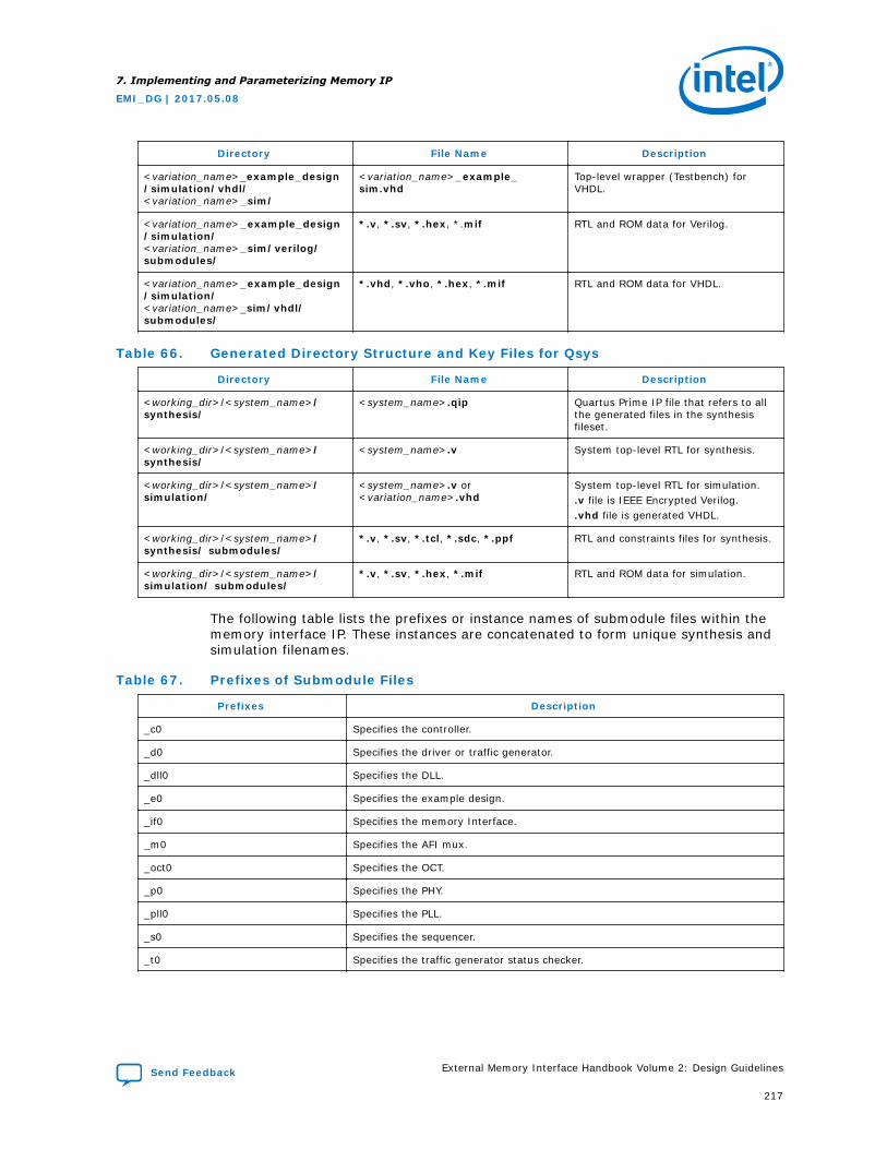
Directory File Name Description
<variation_name>_example_design/simulation/vhdl/ <variation_name>_sim/
<variation_name>_example_sim.vhd
Top-level wrapper (Testbench) forVHDL.
<variation_name>_example_design/simulation/ <variation_name>_sim/verilog/submodules/
*.v, *.sv, *.hex, *.mif RTL and ROM data for Verilog.
<variation_name>_example_design/simulation/ <variation_name>_sim/vhdl/submodules/
*.vhd, *.vho, *.hex, *.mif RTL and ROM data for VHDL.
Table 66. Generated Directory Structure and Key Files for Qsys
Directory File Name Description
<working_dir>/<system_name>/synthesis/
<system_name>.qip Quartus Prime IP file that refers to allthe generated files in the synthesisfileset.
<working_dir>/<system_name>/synthesis/
<system_name>.v System top-level RTL for synthesis.
<working_dir>/<system_name>/simulation/
<system_name>.v or<variation_name>.vhd
System top-level RTL for simulation..v file is IEEE Encrypted Verilog..vhd file is generated VHDL.
<working_dir>/<system_name>/synthesis/ submodules/
*.v, *.sv, *.tcl, *.sdc, *.ppf RTL and constraints files for synthesis.
<working_dir>/<system_name>/simulation/ submodules/
*.v, *.sv, *.hex, *.mif RTL and ROM data for simulation.
The following table lists the prefixes or instance names of submodule files within thememory interface IP. These instances are concatenated to form unique synthesis andsimulation filenames.
Table 67. Prefixes of Submodule Files
Prefixes Description
_c0 Specifies the controller.
_d0 Specifies the driver or traffic generator.
_dll0 Specifies the DLL.
_e0 Specifies the example design.
_if0 Specifies the memory Interface.
_m0 Specifies the AFI mux.
_oct0 Specifies the OCT.
_p0 Specifies the PHY.
_pll0 Specifies the PLL.
_s0 Specifies the sequencer.
_t0 Specifies the traffic generator status checker.
7. Implementing and Parameterizing Memory IP
EMI_DG | 2017.05.08
Send Feedback External Memory Interface Handbook Volume 2: Design Guidelines
217
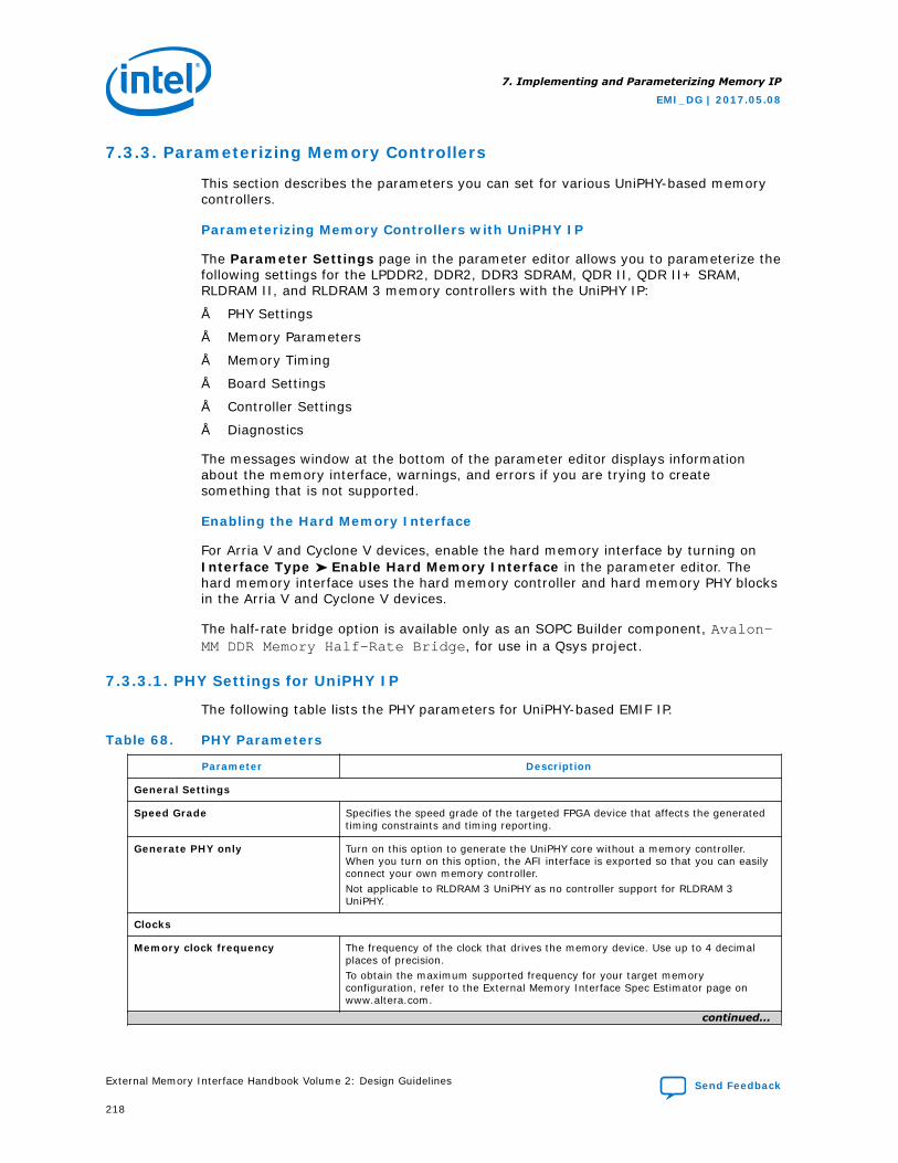
7.3.3. Parameterizing Memory Controllers
This section describes the parameters you can set for various UniPHY-based memorycontrollers.
Parameterizing Memory Controllers with UniPHY IP
The Parameter Settings page in the parameter editor allows you to parameterize thefollowing settings for the LPDDR2, DDR2, DDR3 SDRAM, QDR II, QDR II+ SRAM,RLDRAM II, and RLDRAM 3 memory controllers with the UniPHY IP:
• PHY Settings
• Memory Parameters
• Memory Timing
• Board Settings
• Controller Settings
• Diagnostics
The messages window at the bottom of the parameter editor displays informationabout the memory interface, warnings, and errors if you are trying to createsomething that is not supported.
Enabling the Hard Memory Interface
For Arria V and Cyclone V devices, enable the hard memory interface by turning onInterface Type Enable Hard Memory Interface in the parameter editor. Thehard memory interface uses the hard memory controller and hard memory PHY blocksin the Arria V and Cyclone V devices.
The half-rate bridge option is available only as an SOPC Builder component, Avalon-MM DDR Memory Half-Rate Bridge, for use in a Qsys project.
7.3.3.1. PHY Settings for UniPHY IP
The following table lists the PHY parameters for UniPHY-based EMIF IP.
Table 68. PHY Parameters
Parameter Description
General Settings
Speed Grade Specifies the speed grade of the targeted FPGA device that affects the generatedtiming constraints and timing reporting.
Generate PHY only Turn on this option to generate the UniPHY core without a memory controller.When you turn on this option, the AFI interface is exported so that you can easilyconnect your own memory controller.Not applicable to RLDRAM 3 UniPHY as no controller support for RLDRAM 3UniPHY.
Clocks
Memory clock frequency The frequency of the clock that drives the memory device. Use up to 4 decimalplaces of precision.To obtain the maximum supported frequency for your target memoryconfiguration, refer to the External Memory Interface Spec Estimator page onwww.altera.com.
continued...
7. Implementing and Parameterizing Memory IP
EMI_DG | 2017.05.08
External Memory Interface Handbook Volume 2: Design Guidelines Send Feedback
218
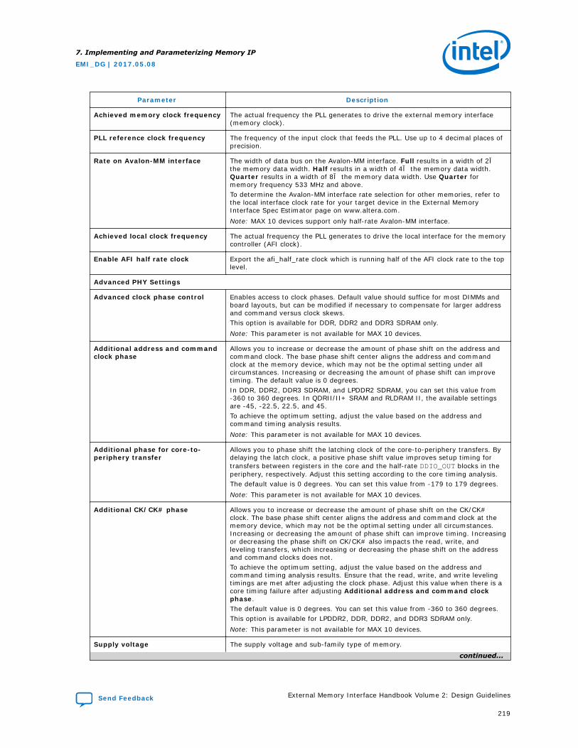
Parameter Description
Achieved memory clock frequency The actual frequency the PLL generates to drive the external memory interface(memory clock).
PLL reference clock frequency The frequency of the input clock that feeds the PLL. Use up to 4 decimal places ofprecision.
Rate on Avalon-MM interface The width of data bus on the Avalon-MM interface. Full results in a width of 2×the memory data width. Half results in a width of 4× the memory data width.Quarter results in a width of 8× the memory data width. Use Quarter formemory frequency 533 MHz and above.To determine the Avalon-MM interface rate selection for other memories, refer tothe local interface clock rate for your target device in the External MemoryInterface Spec Estimator page on www.altera.com.Note: MAX 10 devices support only half-rate Avalon-MM interface.
Achieved local clock frequency The actual frequency the PLL generates to drive the local interface for the memorycontroller (AFI clock).
Enable AFI half rate clock Export the afi_half_rate clock which is running half of the AFI clock rate to the toplevel.
Advanced PHY Settings
Advanced clock phase control Enables access to clock phases. Default value should suffice for most DIMMs andboard layouts, but can be modified if necessary to compensate for larger addressand command versus clock skews.This option is available for DDR, DDR2 and DDR3 SDRAM only.Note: This parameter is not available for MAX 10 devices.
Additional address and commandclock phase
Allows you to increase or decrease the amount of phase shift on the address andcommand clock. The base phase shift center aligns the address and commandclock at the memory device, which may not be the optimal setting under allcircumstances. Increasing or decreasing the amount of phase shift can improvetiming. The default value is 0 degrees.In DDR, DDR2, DDR3 SDRAM, and LPDDR2 SDRAM, you can set this value from-360 to 360 degrees. In QDRII/II+ SRAM and RLDRAM II, the available settingsare -45, -22.5, 22.5, and 45.To achieve the optimum setting, adjust the value based on the address andcommand timing analysis results.Note: This parameter is not available for MAX 10 devices.
Additional phase for core-to-periphery transfer
Allows you to phase shift the latching clock of the core-to-periphery transfers. Bydelaying the latch clock, a positive phase shift value improves setup timing fortransfers between registers in the core and the half-rate DDIO_OUT blocks in theperiphery, respectively. Adjust this setting according to the core timing analysis.The default value is 0 degrees. You can set this value from -179 to 179 degrees.Note: This parameter is not available for MAX 10 devices.
Additional CK/CK# phase Allows you to increase or decrease the amount of phase shift on the CK/CK#clock. The base phase shift center aligns the address and command clock at thememory device, which may not be the optimal setting under all circumstances.Increasing or decreasing the amount of phase shift can improve timing. Increasingor decreasing the phase shift on CK/CK# also impacts the read, write, andleveling transfers, which increasing or decreasing the phase shift on the addressand command clocks does not.To achieve the optimum setting, adjust the value based on the address andcommand timing analysis results. Ensure that the read, write, and write levelingtimings are met after adjusting the clock phase. Adjust this value when there is acore timing failure after adjusting Additional address and command clockphase.The default value is 0 degrees. You can set this value from -360 to 360 degrees.This option is available for LPDDR2, DDR, DDR2, and DDR3 SDRAM only.Note: This parameter is not available for MAX 10 devices.
Supply voltage The supply voltage and sub-family type of memory.
continued...
7. Implementing and Parameterizing Memory IP
EMI_DG | 2017.05.08
Send Feedback External Memory Interface Handbook Volume 2: Design Guidelines
219
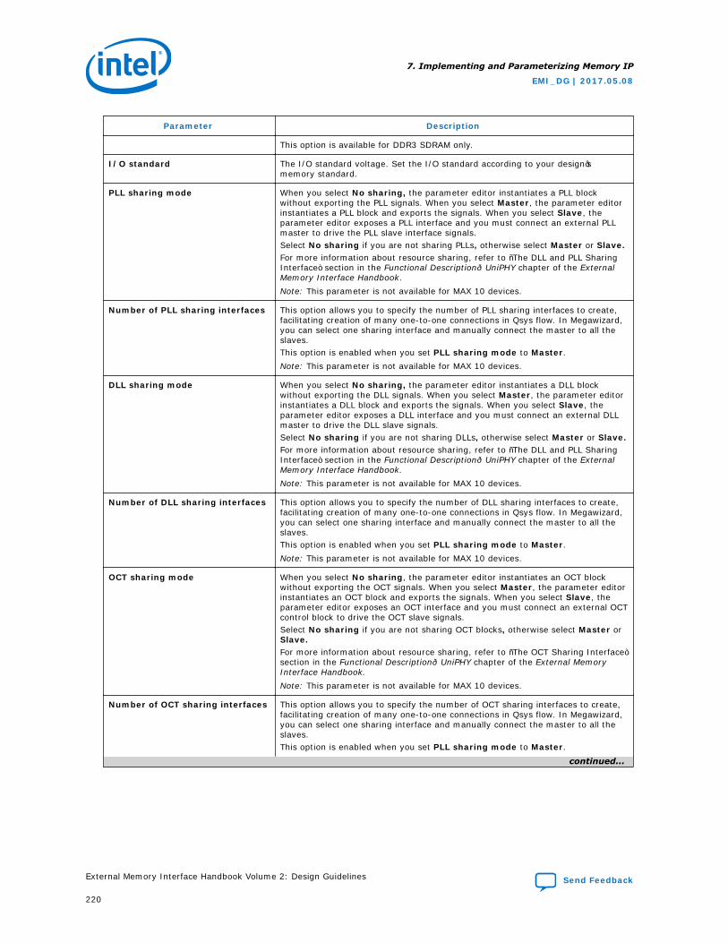
Parameter Description
This option is available for DDR3 SDRAM only.
I/O standard The I/O standard voltage. Set the I/O standard according to your design’smemory standard.
PLL sharing mode When you select No sharing, the parameter editor instantiates a PLL blockwithout exporting the PLL signals. When you select Master, the parameter editorinstantiates a PLL block and exports the signals. When you select Slave, theparameter editor exposes a PLL interface and you must connect an external PLLmaster to drive the PLL slave interface signals.Select No sharing if you are not sharing PLLs, otherwise select Master or Slave.For more information about resource sharing, refer to “The DLL and PLL SharingInterface” section in the Functional Description—UniPHY chapter of the ExternalMemory Interface Handbook.Note: This parameter is not available for MAX 10 devices.
Number of PLL sharing interfaces This option allows you to specify the number of PLL sharing interfaces to create,facilitating creation of many one-to-one connections in Qsys flow. In Megawizard,you can select one sharing interface and manually connect the master to all theslaves.This option is enabled when you set PLL sharing mode to Master.Note: This parameter is not available for MAX 10 devices.
DLL sharing mode When you select No sharing, the parameter editor instantiates a DLL blockwithout exporting the DLL signals. When you select Master, the parameter editorinstantiates a DLL block and exports the signals. When you select Slave, theparameter editor exposes a DLL interface and you must connect an external DLLmaster to drive the DLL slave signals.Select No sharing if you are not sharing DLLs, otherwise select Master or Slave.For more information about resource sharing, refer to “The DLL and PLL SharingInterface” section in the Functional Description—UniPHY chapter of the ExternalMemory Interface Handbook.Note: This parameter is not available for MAX 10 devices.
Number of DLL sharing interfaces This option allows you to specify the number of DLL sharing interfaces to create,facilitating creation of many one-to-one connections in Qsys flow. In Megawizard,you can select one sharing interface and manually connect the master to all theslaves.This option is enabled when you set PLL sharing mode to Master.Note: This parameter is not available for MAX 10 devices.
OCT sharing mode When you select No sharing, the parameter editor instantiates an OCT blockwithout exporting the OCT signals. When you select Master, the parameter editorinstantiates an OCT block and exports the signals. When you select Slave, theparameter editor exposes an OCT interface and you must connect an external OCTcontrol block to drive the OCT slave signals.Select No sharing if you are not sharing OCT blocks, otherwise select Master orSlave.For more information about resource sharing, refer to “The OCT Sharing Interface”section in the Functional Description—UniPHY chapter of the External MemoryInterface Handbook.Note: This parameter is not available for MAX 10 devices.
Number of OCT sharing interfaces This option allows you to specify the number of OCT sharing interfaces to create,facilitating creation of many one-to-one connections in Qsys flow. In Megawizard,you can select one sharing interface and manually connect the master to all theslaves.This option is enabled when you set PLL sharing mode to Master.
continued...
7. Implementing and Parameterizing Memory IP
EMI_DG | 2017.05.08
External Memory Interface Handbook Volume 2: Design Guidelines Send Feedback
220
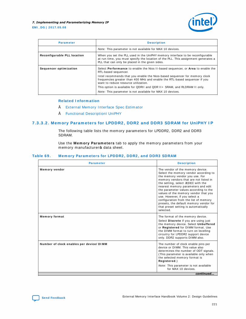
Parameter Description
Note: This parameter is not available for MAX 10 devices.
Reconfigurable PLL location When you set the PLL used in the UniPHY memory interface to be reconfigurableat run time, you must specify the location of the PLL. This assignment generates aPLL that can only be placed in the given sides.
Sequencer optimization Select Performance to enable the Nios II-based sequencer, or Area to enable theRTL-based sequencer.Intel recommends that you enable the Nios-based sequencer for memory clockfrequencies greater than 400 MHz and enable the RTL-based sequencer if youwant to reduce resource utilization.This option is available for QDRII and QDR II+ SRAM, and RLDRAM II only.Note: This parameter is not available for MAX 10 devices.
Related Information
• External Memory Interface Spec Estimator
• Functional Description–UniPHY
7.3.3.2. Memory Parameters for LPDDR2, DDR2 and DDR3 SDRAM for UniPHY IP
The following table lists the memory parameters for LPDDR2, DDR2 and DDR3SDRAM.
Use the Memory Parameters tab to apply the memory parameters from yourmemory manufacturer’s data sheet.
Table 69. Memory Parameters for LPDDR2, DDR2, and DDR3 SDRAM
Parameter Description
Memory vendor The vendor of the memory device.Select the memory vendor according tothe memory vendor you use. Formemory vendors that are not listed inthe setting, select JEDEC with thenearest memory parameters and editthe parameter values according to thevalues of the memory vendor that youuse. However, if you select aconfiguration from the list of memorypresets, the default memory vendor forthat preset setting is automaticallyselected.
Memory format The format of the memory device.Select Discrete if you are using justthe memory device. Select Unbufferedor Registered for DIMM format. Usethe DIMM format to turn on levellingcircuitry for LPDDR2 support deviceonly. DDR2 supports DIMM also.
Number of clock enables per device/DIMM The number of clock enable pins perdevice or DIMM. This value alsodetermines the number of ODT signals.(This parameter is available only whenthe selected memory format isRegistered.)Note: This parameter is not available
for MAX 10 devices.
continued...
7. Implementing and Parameterizing Memory IP
EMI_DG | 2017.05.08
Send Feedback External Memory Interface Handbook Volume 2: Design Guidelines
221
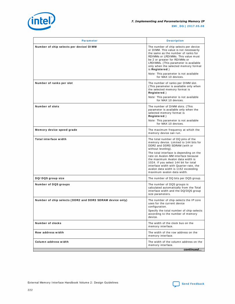
Parameter Description
Number of chip selects per device/DIMM The number of chip selects per deviceor DIMM. This value is not necessarilythe same as the number of ranks forRDIMMs or LRDIMMs. This value mustbe 2 or greater for RDIMMs orLRDIMMs. (This parameter is availableonly when the selected memory formatis Registered.)Note: This parameter is not available
for MAX 10 devices.
Number of ranks per slot The number of ranks per DIMM slot.(This parameter is available only whenthe selected memory format isRegistered.)Note: This parameter is not available
for MAX 10 devices.
Number of slots The number of DIMM slots. (Thisparameter is available only when theselected memory format isRegistered.)Note: This parameter is not available
for MAX 10 devices.
Memory device speed grade The maximum frequency at which thememory device can run.
Total interface width The total number of DQ pins of thememory device. Limited to 144 bits forDDR2 and DDR3 SDRAM (with orwithout leveling).The total interface is depending on therate on Avalon-MM interface becausethe maximum Avalon data width is1024. If you select 144 bit for totalinterface width with Quarter-rate, theavalon data width is 1152 exceedingmaximum avalon data width.
DQ/DQS group size The number of DQ bits per DQS group.
Number of DQS groups The number of DQS groups iscalculated automatically from the Totalinterface width and the DQ/DQS groupsize parameters.
Number of chip selects (DDR2 and DDR3 SDRAM device only) The number of chip-selects the IP coreuses for the current deviceconfiguration.Specify the total number of chip-selectsaccording to the number of memorydevice.
Number of clocks The width of the clock bus on thememory interface.
Row address width The width of the row address on thememory interface.
Column address width The width of the column address on thememory interface.
continued...
7. Implementing and Parameterizing Memory IP
EMI_DG | 2017.05.08
External Memory Interface Handbook Volume 2: Design Guidelines Send Feedback
222
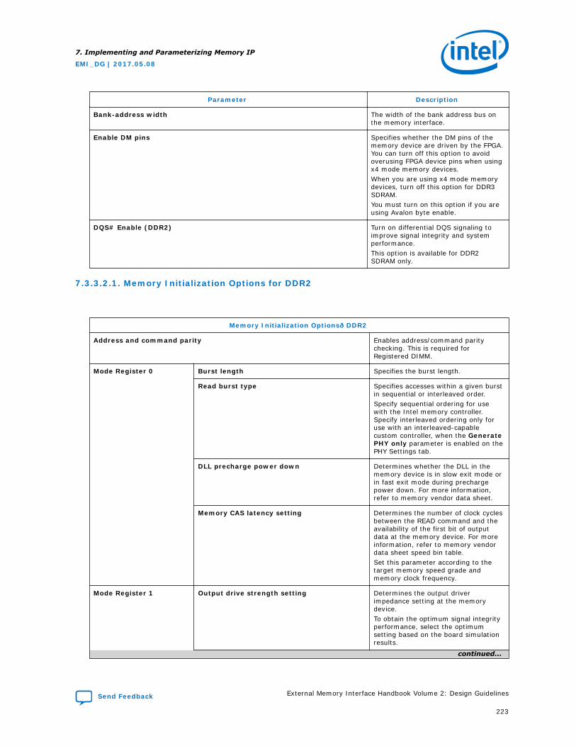
Parameter Description
Bank-address width The width of the bank address bus onthe memory interface.
Enable DM pins Specifies whether the DM pins of thememory device are driven by the FPGA.You can turn off this option to avoidoverusing FPGA device pins when usingx4 mode memory devices.When you are using x4 mode memorydevices, turn off this option for DDR3SDRAM.You must turn on this option if you areusing Avalon byte enable.
DQS# Enable (DDR2) Turn on differential DQS signaling toimprove signal integrity and systemperformance.This option is available for DDR2SDRAM only.
7.3.3.2.1. Memory Initialization Options for DDR2
Memory Initialization Options—DDR2
Address and command parity Enables address/command paritychecking. This is required forRegistered DIMM.
Mode Register 0 Burst length Specifies the burst length.
Read burst type Specifies accesses within a given burstin sequential or interleaved order.Specify sequential ordering for usewith the Intel memory controller.Specify interleaved ordering only foruse with an interleaved-capablecustom controller, when the GeneratePHY only parameter is enabled on thePHY Settings tab.
DLL precharge power down Determines whether the DLL in thememory device is in slow exit mode orin fast exit mode during prechargepower down. For more information,refer to memory vendor data sheet.
Memory CAS latency setting Determines the number of clock cyclesbetween the READ command and theavailability of the first bit of outputdata at the memory device. For moreinformation, refer to memory vendordata sheet speed bin table.Set this parameter according to thetarget memory speed grade andmemory clock frequency.
Mode Register 1 Output drive strength setting Determines the output driverimpedance setting at the memorydevice.To obtain the optimum signal integrityperformance, select the optimumsetting based on the board simulationresults.
continued...
7. Implementing and Parameterizing Memory IP
EMI_DG | 2017.05.08
Send Feedback External Memory Interface Handbook Volume 2: Design Guidelines
223
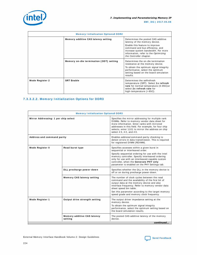
Memory Initialization Options—DDR2
Memory additive CAS latency setting Determines the posted CAS additivelatency of the memory device.Enable this feature to improvecommand and bus efficiency, andincrease system bandwidth. For moreinformation, refer to the Optimizingthe Controller chapter.
Memory on-die termination (ODT) setting Determines the on-die terminationresistance at the memory device.To obtain the optimum signal integrityperformance, select the optimumsetting based on the board simulationresults.
Mode Register 2 SRT Enable Determines the selfrefreshtemperature (SRT). Select 1x refreshrate for normal temperature (0-85C)orselect 2x refresh rate forhigh-temperature (>85C).
7.3.3.2.2. Memory Initialization Options for DDR3
Memory Initialization Options—DDR3
Mirror Addressing: 1 per chip select Specifies the mirror addressing for multiple rankDIMMs. Refer to memory vendor data sheet formore information. Enter ranks with mirroredaddresses in this field. For example, for four chipselects, enter 1101 to mirror the address on chipselect #3, #2, and #0.
Address and command parity Enables address/command parity checking todetect errors in data transmission. This is requiredfor registered DIMM (RDIMM).
Mode Register 0 Read burst type Specifies accesses within a given burst insequential or interleaved order.Specify sequential ordering for use with the Intelmemory controller. Specify interleaved orderingonly for use with an interleaved-capable customcontroller, when the Generate PHY onlyparameter is enabled on the PHY Settings tab.
DLL precharge power down Specifies whether the DLL in the memory device isoff or on during precharge power-down.
Memory CAS latency setting The number of clock cycles between the readcommand and the availability of the first bit ofoutput data at the memory device and alsointerface frequency. Refer to memory vendor datasheet speed bin table.Set this parameter according to the target memoryspeed grade and memory clock frequency.
Mode Register 1 Output drive strength setting The output driver impedance setting at thememory device.To obtain the optimum signal integrityperformance, select the optimum setting based onthe board simulation results.
Memory additive CAS latencysetting
The posted CAS additive latency of the memorydevice.
continued...
7. Implementing and Parameterizing Memory IP
EMI_DG | 2017.05.08
External Memory Interface Handbook Volume 2: Design Guidelines Send Feedback
224
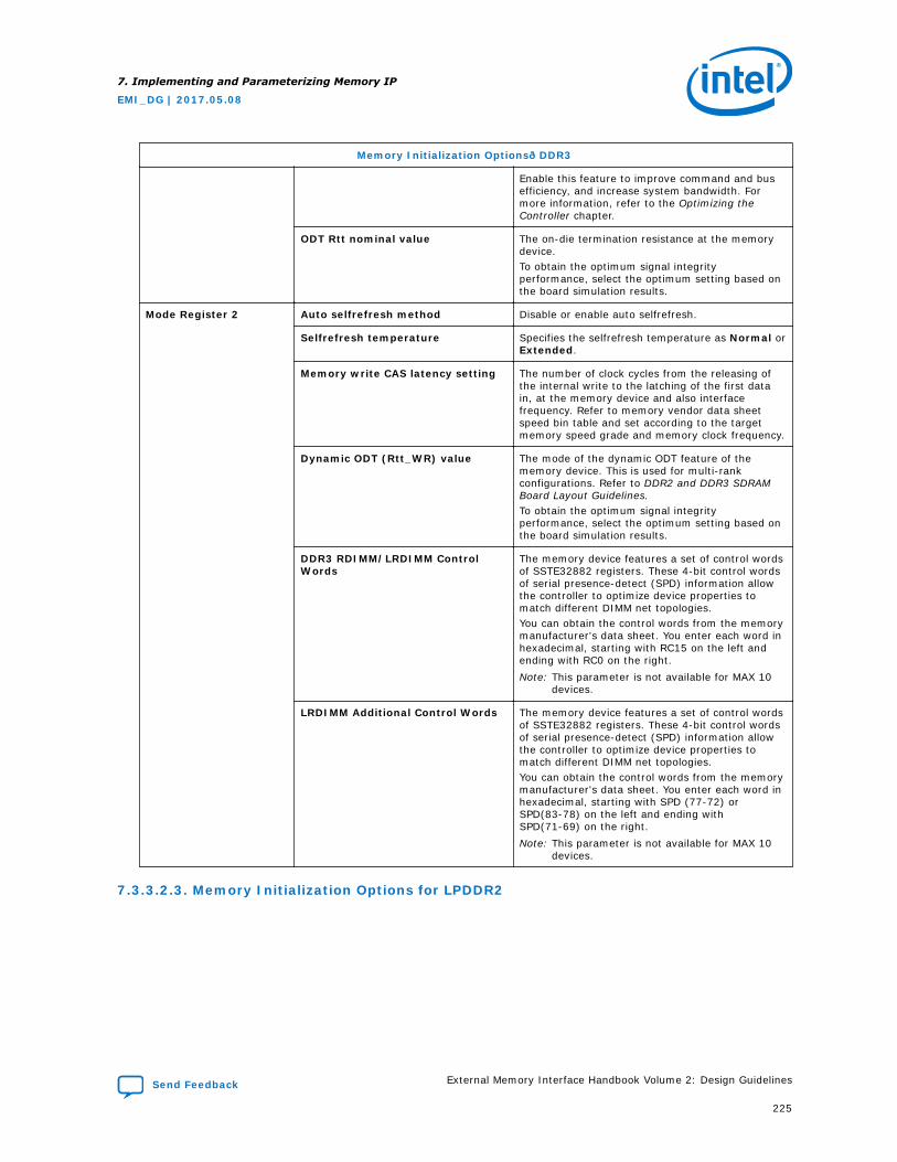
Memory Initialization Options—DDR3
Enable this feature to improve command and busefficiency, and increase system bandwidth. Formore information, refer to the Optimizing theController chapter.
ODT Rtt nominal value The on-die termination resistance at the memorydevice.To obtain the optimum signal integrityperformance, select the optimum setting based onthe board simulation results.
Mode Register 2 Auto selfrefresh method Disable or enable auto selfrefresh.
Selfrefresh temperature Specifies the selfrefresh temperature as Normal orExtended.
Memory write CAS latency setting The number of clock cycles from the releasing ofthe internal write to the latching of the first datain, at the memory device and also interfacefrequency. Refer to memory vendor data sheetspeed bin table and set according to the targetmemory speed grade and memory clock frequency.
Dynamic ODT (Rtt_WR) value The mode of the dynamic ODT feature of thememory device. This is used for multi-rankconfigurations. Refer to DDR2 and DDR3 SDRAMBoard Layout Guidelines.To obtain the optimum signal integrityperformance, select the optimum setting based onthe board simulation results.
DDR3 RDIMM/LRDIMM ControlWords
The memory device features a set of control wordsof SSTE32882 registers. These 4-bit control wordsof serial presence-detect (SPD) information allowthe controller to optimize device properties tomatch different DIMM net topologies.You can obtain the control words from the memorymanufacturer's data sheet. You enter each word inhexadecimal, starting with RC15 on the left andending with RC0 on the right.Note: This parameter is not available for MAX 10
devices.
LRDIMM Additional Control Words The memory device features a set of control wordsof SSTE32882 registers. These 4-bit control wordsof serial presence-detect (SPD) information allowthe controller to optimize device properties tomatch different DIMM net topologies.You can obtain the control words from the memorymanufacturer's data sheet. You enter each word inhexadecimal, starting with SPD (77-72) orSPD(83-78) on the left and ending withSPD(71-69) on the right.Note: This parameter is not available for MAX 10
devices.
7.3.3.2.3. Memory Initialization Options for LPDDR2
7. Implementing and Parameterizing Memory IP
EMI_DG | 2017.05.08
Send Feedback External Memory Interface Handbook Volume 2: Design Guidelines
225
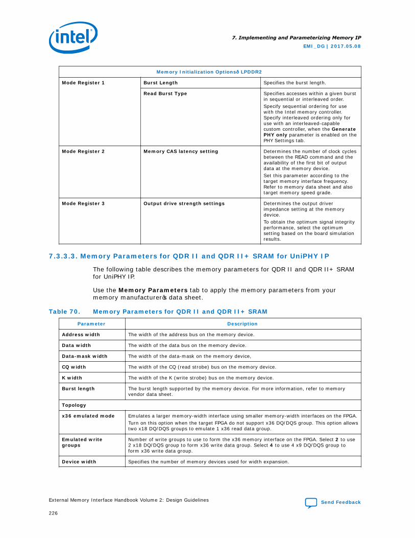
Memory Initialization Options—LPDDR2
Mode Register 1 Burst Length Specifies the burst length.
Read Burst Type Specifies accesses within a given burstin sequential or interleaved order.Specify sequential ordering for usewith the Intel memory controller.Specify interleaved ordering only foruse with an interleaved-capablecustom controller, when the GeneratePHY only parameter is enabled on thePHY Settings tab.
Mode Register 2 Memory CAS latency setting Determines the number of clock cyclesbetween the READ command and theavailability of the first bit of outputdata at the memory device.Set this parameter according to thetarget memory interface frequency.Refer to memory data sheet and alsotarget memory speed grade.
Mode Register 3 Output drive strength settings Determines the output driverimpedance setting at the memorydevice.To obtain the optimum signal integrityperformance, select the optimumsetting based on the board simulationresults.
7.3.3.3. Memory Parameters for QDR II and QDR II+ SRAM for UniPHY IP
The following table describes the memory parameters for QDR II and QDR II+ SRAMfor UniPHY IP.
Use the Memory Parameters tab to apply the memory parameters from yourmemory manufacturer’s data sheet.
Table 70. Memory Parameters for QDR II and QDR II+ SRAM
Parameter Description
Address width The width of the address bus on the memory device.
Data width The width of the data bus on the memory device.
Data-mask width The width of the data-mask on the memory device,
CQ width The width of the CQ (read strobe) bus on the memory device.
K width The width of the K (write strobe) bus on the memory device.
Burst length The burst length supported by the memory device. For more information, refer to memoryvendor data sheet.
Topology
x36 emulated mode Emulates a larger memory-width interface using smaller memory-width interfaces on the FPGA.Turn on this option when the target FPGA do not support x36 DQ/DQS group. This option allowstwo x18 DQ/DQS groups to emulate 1 x36 read data group.
Emulated writegroups
Number of write groups to use to form the x36 memory interface on the FPGA. Select 2 to use2 x18 DQ/DQS group to form x36 write data group. Select 4 to use 4 x9 DQ/DQS group toform x36 write data group.
Device width Specifies the number of memory devices used for width expansion.
7. Implementing and Parameterizing Memory IP
EMI_DG | 2017.05.08
External Memory Interface Handbook Volume 2: Design Guidelines Send Feedback
226
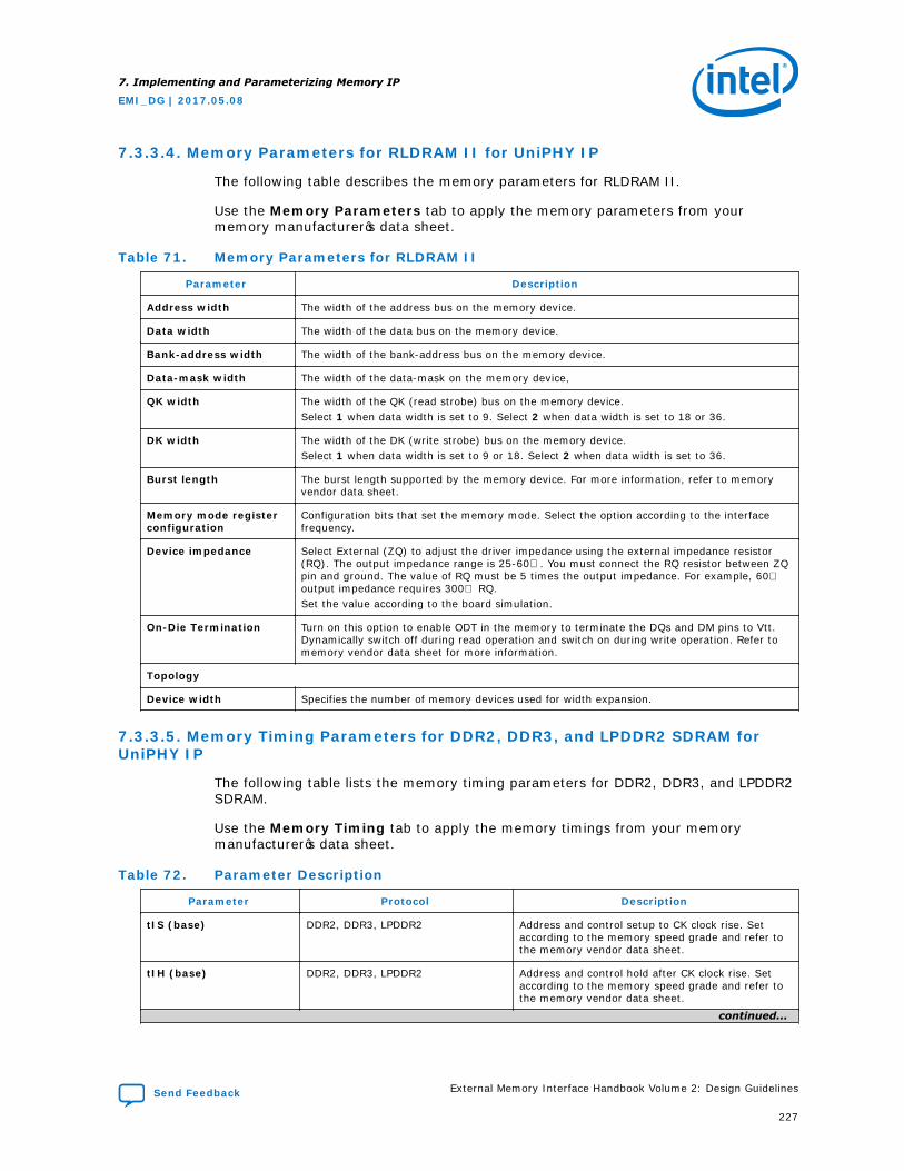
7.3.3.4. Memory Parameters for RLDRAM II for UniPHY IP
The following table describes the memory parameters for RLDRAM II.
Use the Memory Parameters tab to apply the memory parameters from yourmemory manufacturer’s data sheet.
Table 71. Memory Parameters for RLDRAM II
Parameter Description
Address width The width of the address bus on the memory device.
Data width The width of the data bus on the memory device.
Bank-address width The width of the bank-address bus on the memory device.
Data-mask width The width of the data-mask on the memory device,
QK width The width of the QK (read strobe) bus on the memory device.Select 1 when data width is set to 9. Select 2 when data width is set to 18 or 36.
DK width The width of the DK (write strobe) bus on the memory device.Select 1 when data width is set to 9 or 18. Select 2 when data width is set to 36.
Burst length The burst length supported by the memory device. For more information, refer to memoryvendor data sheet.
Memory mode registerconfiguration
Configuration bits that set the memory mode. Select the option according to the interfacefrequency.
Device impedance Select External (ZQ) to adjust the driver impedance using the external impedance resistor(RQ). The output impedance range is 25-60. You must connect the RQ resistor between ZQpin and ground. The value of RQ must be 5 times the output impedance. For example, 60output impedance requires 300 RQ.Set the value according to the board simulation.
On-Die Termination Turn on this option to enable ODT in the memory to terminate the DQs and DM pins to Vtt.Dynamically switch off during read operation and switch on during write operation. Refer tomemory vendor data sheet for more information.
Topology
Device width Specifies the number of memory devices used for width expansion.
7.3.3.5. Memory Timing Parameters for DDR2, DDR3, and LPDDR2 SDRAM forUniPHY IP
The following table lists the memory timing parameters for DDR2, DDR3, and LPDDR2SDRAM.
Use the Memory Timing tab to apply the memory timings from your memorymanufacturer’s data sheet.
Table 72. Parameter Description
Parameter Protocol Description
tIS (base) DDR2, DDR3, LPDDR2 Address and control setup to CK clock rise. Setaccording to the memory speed grade and refer tothe memory vendor data sheet.
tIH (base) DDR2, DDR3, LPDDR2 Address and control hold after CK clock rise. Setaccording to the memory speed grade and refer tothe memory vendor data sheet.
continued...
7. Implementing and Parameterizing Memory IP
EMI_DG | 2017.05.08
Send Feedback External Memory Interface Handbook Volume 2: Design Guidelines
227
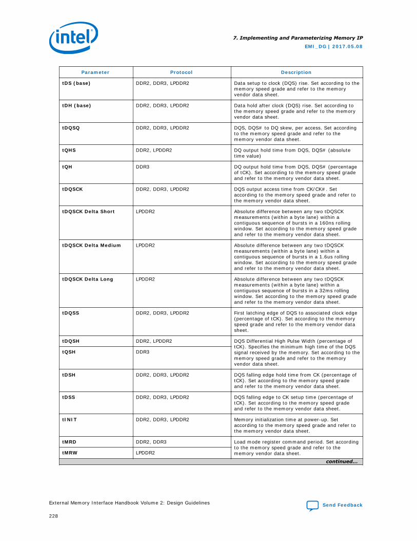
Parameter Protocol Description
tDS (base) DDR2, DDR3, LPDDR2 Data setup to clock (DQS) rise. Set according to thememory speed grade and refer to the memoryvendor data sheet.
tDH (base) DDR2, DDR3, LPDDR2 Data hold after clock (DQS) rise. Set according tothe memory speed grade and refer to the memoryvendor data sheet.
tDQSQ DDR2, DDR3, LPDDR2 DQS, DQS# to DQ skew, per access. Set accordingto the memory speed grade and refer to thememory vendor data sheet.
tQHS DDR2, LPDDR2 DQ output hold time from DQS, DQS# (absolutetime value)
tQH DDR3 DQ output hold time from DQS, DQS# (percentageof tCK). Set according to the memory speed gradeand refer to the memory vendor data sheet.
tDQSCK DDR2, DDR3, LPDDR2 DQS output access time from CK/CK#. Setaccording to the memory speed grade and refer tothe memory vendor data sheet.
tDQSCK Delta Short LPDDR2 Absolute difference between any two tDQSCKmeasurements (within a byte lane) within acontiguous sequence of bursts in a 160ns rollingwindow. Set according to the memory speed gradeand refer to the memory vendor data sheet.
tDQSCK Delta Medium LPDDR2 Absolute difference between any two tDQSCKmeasurements (within a byte lane) within acontiguous sequence of bursts in a 1.6us rollingwindow. Set according to the memory speed gradeand refer to the memory vendor data sheet.
tDQSCK Delta Long LPDDR2 Absolute difference between any two tDQSCKmeasurements (within a byte lane) within acontiguous sequence of bursts in a 32ms rollingwindow. Set according to the memory speed gradeand refer to the memory vendor data sheet.
tDQSS DDR2, DDR3, LPDDR2 First latching edge of DQS to associated clock edge(percentage of tCK). Set according to the memoryspeed grade and refer to the memory vendor datasheet.
tDQSH DDR2, LPDDR2 DQS Differential High Pulse Width (percentage oftCK). Specifies the minimum high time of the DQSsignal received by the memory. Set according to thememory speed grade and refer to the memoryvendor data sheet.
tQSH DDR3
tDSH DDR2, DDR3, LPDDR2 DQS falling edge hold time from CK (percentage oftCK). Set according to the memory speed gradeand refer to the memory vendor data sheet.
tDSS DDR2, DDR3, LPDDR2 DQS falling edge to CK setup time (percentage oftCK). Set according to the memory speed gradeand refer to the memory vendor data sheet.
tINIT DDR2, DDR3, LPDDR2 Memory initialization time at power-up. Setaccording to the memory speed grade and refer tothe memory vendor data sheet.
tMRD DDR2, DDR3 Load mode register command period. Set accordingto the memory speed grade and refer to thememory vendor data sheet.tMRW LPDDR2
continued...
7. Implementing and Parameterizing Memory IP
EMI_DG | 2017.05.08
External Memory Interface Handbook Volume 2: Design Guidelines Send Feedback
228
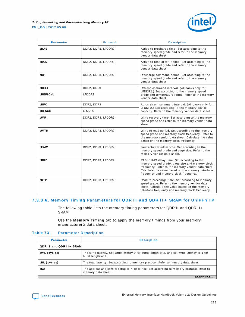
Parameter Protocol Description
tRAS DDR2, DDR3, LPDDR2 Active to precharge time. Set according to thememory speed grade and refer to the memoryvendor data sheet.
tRCD DDR2, DDR3, LPDDR2 Active to read or write time. Set according to thememory speed grade and refer to the memoryvendor data sheet.
tRP DDR2, DDR3, LPDDR2 Precharge command period. Set according to thememory speed grade and refer to the memoryvendor data sheet.
tREFI DDR2, DDR3 Refresh command interval. (All banks only forLPDDR2.) Set according to the memory speedgrade and temperature range. Refer to the memoryvendor data sheet.
tREFICab LPDDR2
tRFC DDR2, DDR3 Auto-refresh command interval. (All banks only forLPDDR2.) Set according to the memory devicecapacity. Refer to the memory vendor data sheet.tRFCab LPDDR2
tWR DDR2, DDR3, LPDDR2 Write recovery time. Set according to the memoryspeed grade and refer to the memory vendor datasheet.
tWTR DDR2, DDR3, LPDDR2 Write to read period. Set according to the memoryspeed grade and memory clock frequency. Refer tothe memory vendor data sheet. Calculate the valuebased on the memory clock frequency.
tFAW DDR2, DDR3, LPDDR2 Four active window time. Set according to thememory speed grade and page size. Refer to thememory vendor data sheet.
tRRD DDR2, DDR3, LPDDR2 RAS to RAS delay time. Set according to thememory speed grade, page size and memory clockfrequency. Refer to the memory vendor data sheet.Calculate the value based on the memory interfacefrequency and memory clock frequency.
tRTP DDR2, DDR3, LPDDR2 Read to precharge time. Set according to memoryspeed grade. Refer to the memory vendor datasheet. Calculate the value based on the memoryinterface frequency and memory clock frequency.
7.3.3.6. Memory Timing Parameters for QDR II and QDR II+ SRAM for UniPHY IP
The following table lists the memory timing parameters for QDR II and QDR II+SRAM.
Use the Memory Timing tab to apply the memory timings from your memorymanufacturer’s data sheet.
Table 73. Parameter Description
Parameter Description
QDR II and QDR II+ SRAM
tWL (cycles) The write latency. Set write latency 0 for burst length of 2, and set write latency to 1 forburst length of 4.
tRL (cycles) The read latency. Set according to memory protocol. Refer to memory data sheet.
tSA The address and control setup to K clock rise. Set according to memory protocol. Refer tomemory data sheet.
continued...
7. Implementing and Parameterizing Memory IP
EMI_DG | 2017.05.08
Send Feedback External Memory Interface Handbook Volume 2: Design Guidelines
229
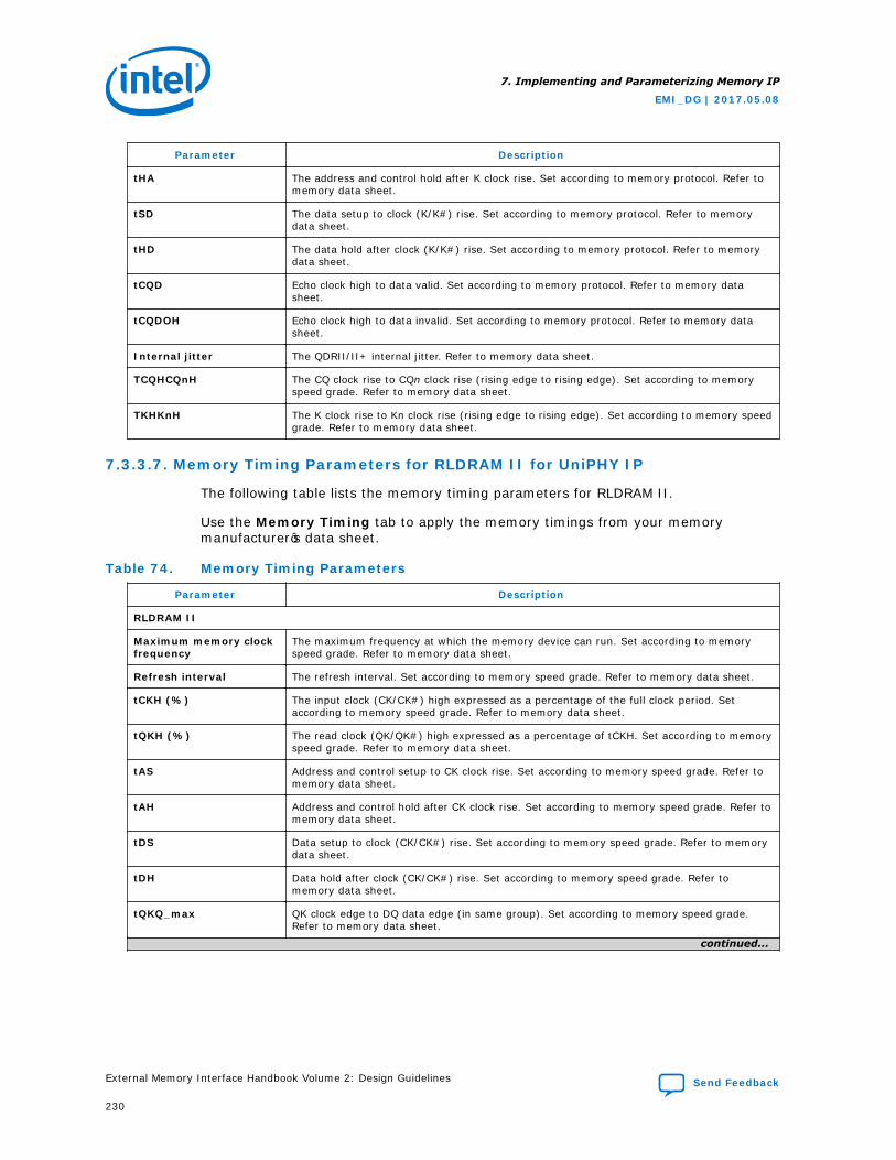
Parameter Description
tHA The address and control hold after K clock rise. Set according to memory protocol. Refer tomemory data sheet.
tSD The data setup to clock (K/K#) rise. Set according to memory protocol. Refer to memorydata sheet.
tHD The data hold after clock (K/K#) rise. Set according to memory protocol. Refer to memorydata sheet.
tCQD Echo clock high to data valid. Set according to memory protocol. Refer to memory datasheet.
tCQDOH Echo clock high to data invalid. Set according to memory protocol. Refer to memory datasheet.
Internal jitter The QDRII/II+ internal jitter. Refer to memory data sheet.
TCQHCQnH The CQ clock rise to CQn clock rise (rising edge to rising edge). Set according to memoryspeed grade. Refer to memory data sheet.
TKHKnH The K clock rise to Kn clock rise (rising edge to rising edge). Set according to memory speedgrade. Refer to memory data sheet.
7.3.3.7. Memory Timing Parameters for RLDRAM II for UniPHY IP
The following table lists the memory timing parameters for RLDRAM II.
Use the Memory Timing tab to apply the memory timings from your memorymanufacturer’s data sheet.
Table 74. Memory Timing Parameters
Parameter Description
RLDRAM II
Maximum memory clockfrequency
The maximum frequency at which the memory device can run. Set according to memoryspeed grade. Refer to memory data sheet.
Refresh interval The refresh interval. Set according to memory speed grade. Refer to memory data sheet.
tCKH (%) The input clock (CK/CK#) high expressed as a percentage of the full clock period. Setaccording to memory speed grade. Refer to memory data sheet.
tQKH (%) The read clock (QK/QK#) high expressed as a percentage of tCKH. Set according to memoryspeed grade. Refer to memory data sheet.
tAS Address and control setup to CK clock rise. Set according to memory speed grade. Refer tomemory data sheet.
tAH Address and control hold after CK clock rise. Set according to memory speed grade. Refer tomemory data sheet.
tDS Data setup to clock (CK/CK#) rise. Set according to memory speed grade. Refer to memorydata sheet.
tDH Data hold after clock (CK/CK#) rise. Set according to memory speed grade. Refer tomemory data sheet.
tQKQ_max QK clock edge to DQ data edge (in same group). Set according to memory speed grade.Refer to memory data sheet.
continued...
7. Implementing and Parameterizing Memory IP
EMI_DG | 2017.05.08
External Memory Interface Handbook Volume 2: Design Guidelines Send Feedback
230
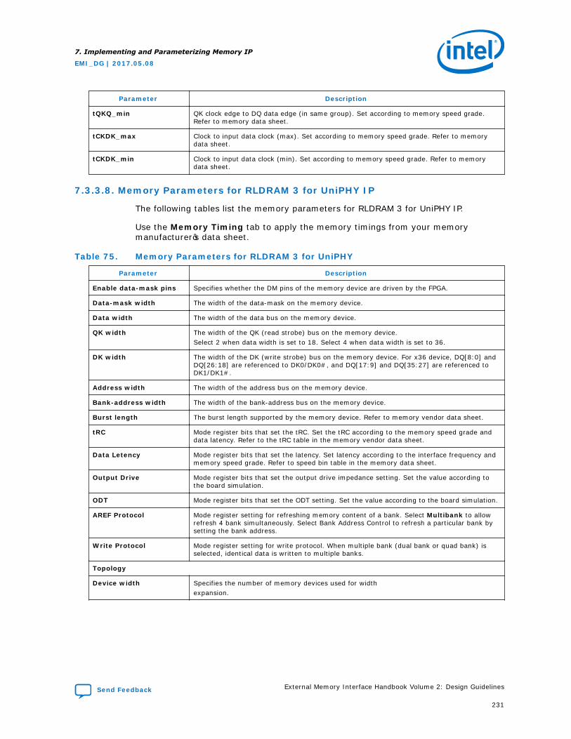
Parameter Description
tQKQ_min QK clock edge to DQ data edge (in same group). Set according to memory speed grade.Refer to memory data sheet.
tCKDK_max Clock to input data clock (max). Set according to memory speed grade. Refer to memorydata sheet.
tCKDK_min Clock to input data clock (min). Set according to memory speed grade. Refer to memorydata sheet.
7.3.3.8. Memory Parameters for RLDRAM 3 for UniPHY IP
The following tables list the memory parameters for RLDRAM 3 for UniPHY IP.
Use the Memory Timing tab to apply the memory timings from your memorymanufacturer’s data sheet.
Table 75. Memory Parameters for RLDRAM 3 for UniPHY
Parameter Description
Enable data-mask pins Specifies whether the DM pins of the memory device are driven by the FPGA.
Data-mask width The width of the data-mask on the memory device.
Data width The width of the data bus on the memory device.
QK width The width of the QK (read strobe) bus on the memory device.Select 2 when data width is set to 18. Select 4 when data width is set to 36.
DK width The width of the DK (write strobe) bus on the memory device. For x36 device, DQ[8:0] andDQ[26:18] are referenced to DK0/DK0#, and DQ[17:9] and DQ[35:27] are referenced toDK1/DK1#.
Address width The width of the address bus on the memory device.
Bank-address width The width of the bank-address bus on the memory device.
Burst length The burst length supported by the memory device. Refer to memory vendor data sheet.
tRC Mode register bits that set the tRC. Set the tRC according to the memory speed grade anddata latency. Refer to the tRC table in the memory vendor data sheet.
Data Letency Mode register bits that set the latency. Set latency according to the interface frequency andmemory speed grade. Refer to speed bin table in the memory data sheet.
Output Drive Mode register bits that set the output drive impedance setting. Set the value according tothe board simulation.
ODT Mode register bits that set the ODT setting. Set the value according to the board simulation.
AREF Protocol Mode register setting for refreshing memory content of a bank. Select Multibank to allowrefresh 4 bank simultaneously. Select Bank Address Control to refresh a particular bank bysetting the bank address.
Write Protocol Mode register setting for write protocol. When multiple bank (dual bank or quad bank) isselected, identical data is written to multiple banks.
Topology
Device width Specifies the number of memory devices used for widthexpansion.
7. Implementing and Parameterizing Memory IP
EMI_DG | 2017.05.08
Send Feedback External Memory Interface Handbook Volume 2: Design Guidelines
231
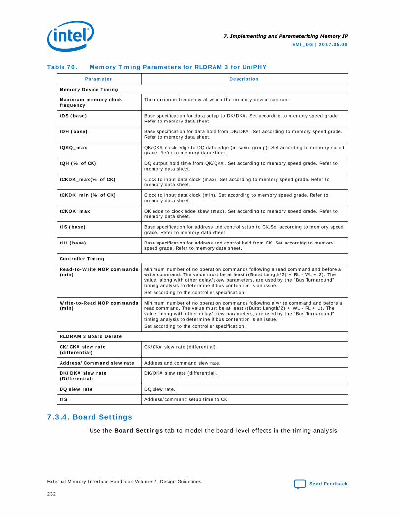
Table 76. Memory Timing Parameters for RLDRAM 3 for UniPHY
Parameter Description
Memory Device Timing
Maximum memory clockfrequency
The maximum frequency at which the memory device can run.
tDS (base) Base specification for data setup to DK/DK#. Set according to memory speed grade.Refer to memory data sheet.
tDH (base) Base specification for data hold from DK/DK#. Set according to memory speed grade.Refer to memory data sheet.
tQKQ_max QK/QK# clock edge to DQ data edge (in same group). Set according to memory speedgrade. Refer to memory data sheet.
tQH (% of CK) DQ output hold time from QK/QK#. Set according to memory speed grade. Refer tomemory data sheet.
tCKDK_max(% of CK) Clock to input data clock (max). Set according to memory speed grade. Refer tomemory data sheet.
tCKDK_min (% of CK) Clock to input data clock (min). Set according to memory speed grade. Refer tomemory data sheet.
tCKQK_max QK edge to clock edge skew (max). Set according to memory speed grade. Refer tomemory data sheet.
tIS (base) Base specification for address and control setup to CK.Set according to memory speedgrade. Refer to memory data sheet.
tIH (base) Base specification for address and control hold from CK. Set according to memoryspeed grade. Refer to memory data sheet.
Controller Timing
Read-to-Write NOP commands(min)
Minimum number of no operation commands following a read command and before awrite command. The value must be at least ((Burst Length/2) + RL - WL + 2). Thevalue, along with other delay/skew parameters, are used by the "Bus Turnaround"timing analysis to determine if bus contention is an issue.Set according to the controller specification.
Write-to-Read NOP commands(min)
Minimum number of no operation commands following a write command and before aread command. The value must be at least ((Burst Length/2) + WL - RL + 1). Thevalue, along with other delay/skew parameters, are used by the "Bus Turnaround"timing analysis to determine if bus contention is an issue.Set according to the controller specification.
RLDRAM 3 Board Derate
CK/CK# slew rate(differential)
CK/CK# slew rate (differential).
Address/Command slew rate Address and command slew rate.
DK/DK# slew rate(Differential)
DK/DK# slew rate (differential).
DQ slew rate DQ slew rate.
tIS Address/command setup time to CK.
7.3.4. Board Settings
Use the Board Settings tab to model the board-level effects in the timing analysis.
7. Implementing and Parameterizing Memory IP
EMI_DG | 2017.05.08
External Memory Interface Handbook Volume 2: Design Guidelines Send Feedback
232
The Board Settings tab allows you to specify the following settings:
• Setup and hold derating (For LPDDR2/DDR2/DDR3 SDRAM, RLDRAM 3 andRLDRAM II for UniPHY IP)
• Channel Signal Integrity
• Board skews (For UniPHY IP.)
Note: For accurate timing results, you must enter board settings parameters that are correctfor your PCB.
The IP core supports single and multiple chip-select configurations. Intel hasdetermined the effects on the output signaling of single-rank configurations for certainIntel boards, and included the channel uncertainties in the Quartus Prime timingmodels.
Because the Quartus Prime timing models hold channel uncertainties that arerepresentative of specific Intel boards, you must determine the board-level effects ofyour board, including any additional channel uncertainty relative to Intel's referencedesign, and enter those values into the Board Settings panel in the parameter editor.You can use HyperLynx or a similar simulator to obtain values that are representativeof your board.
For more information about how to include your board simulation results in theQuartus Prime software, refer to the following sections. For more information abouthow to assign pins using pin planners, refer to the design flow tutorials and designexamples on the List of Designs Using Intel External Memory IP page ofwww.alterawiki.com.
For more general information about timing deration methodology, refer to the TimingDeration Methodology for Multiple Chip Select DDR2 and DDR3 SDRAM Designs sectionin the Analyzing Timing of Memory IP chapter.
Related Information
• Analyzing Timing of Memory IP
• List of Designs using Intel External Memory IP
7.3.4.1. Setup and Hold Derating for UniPHY IP
The slew rate of the output signals affects the setup and hold times of the memorydevice, and thus the write margin. You can specify the slew rate of the output signalsto see their effect on the setup and hold times of both the address and commandsignals and the DQ signals, or alternatively, you may want to specify the setup andhold times directly.
For RDIMMs, the slew rate is defined at the register on the RDIMM, instead of at thememory component. For LRDIMMs, the slew rate is defined at the buffer on theLRDIMM, instead of at the memory component.
Note: You should enter information derived during your PCB development process ofprelayout (line) and postlayout (board) simulation.
The following table lists the setup and hold derating parameters.
7. Implementing and Parameterizing Memory IP
EMI_DG | 2017.05.08
Send Feedback External Memory Interface Handbook Volume 2: Design Guidelines
233
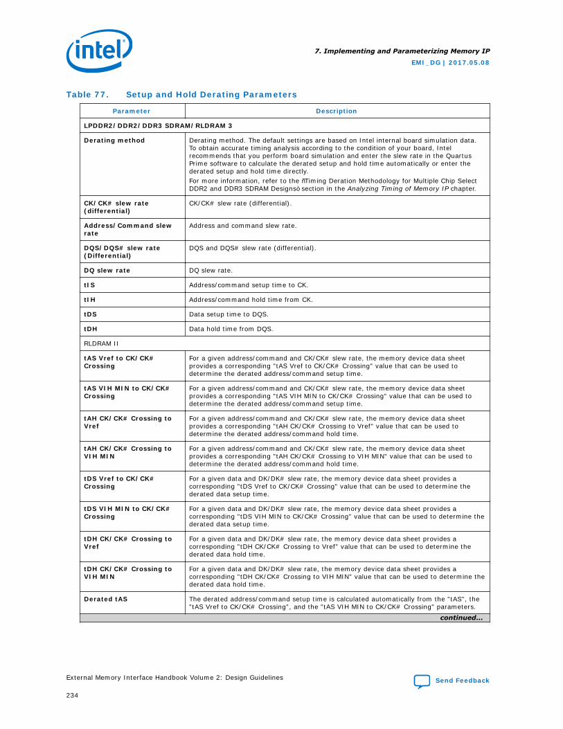
Table 77. Setup and Hold Derating Parameters
Parameter Description
LPDDR2/DDR2/DDR3 SDRAM/RLDRAM 3
Derating method Derating method. The default settings are based on Intel internal board simulation data.To obtain accurate timing analysis according to the condition of your board, Intelrecommends that you perform board simulation and enter the slew rate in the QuartusPrime software to calculate the derated setup and hold time automatically or enter thederated setup and hold time directly.For more information, refer to the “Timing Deration Methodology for Multiple Chip SelectDDR2 and DDR3 SDRAM Designs” section in the Analyzing Timing of Memory IP chapter.
CK/CK# slew rate(differential)
CK/CK# slew rate (differential).
Address/Command slewrate
Address and command slew rate.
DQS/DQS# slew rate(Differential)
DQS and DQS# slew rate (differential).
DQ slew rate DQ slew rate.
tIS Address/command setup time to CK.
tIH Address/command hold time from CK.
tDS Data setup time to DQS.
tDH Data hold time from DQS.
RLDRAM II
tAS Vref to CK/CK#Crossing
For a given address/command and CK/CK# slew rate, the memory device data sheetprovides a corresponding "tAS Vref to CK/CK# Crossing" value that can be used todetermine the derated address/command setup time.
tAS VIH MIN to CK/CK#Crossing
For a given address/command and CK/CK# slew rate, the memory device data sheetprovides a corresponding "tAS VIH MIN to CK/CK# Crossing" value that can be used todetermine the derated address/command setup time.
tAH CK/CK# Crossing toVref
For a given address/command and CK/CK# slew rate, the memory device data sheetprovides a corresponding "tAH CK/CK# Crossing to Vref" value that can be used todetermine the derated address/command hold time.
tAH CK/CK# Crossing toVIH MIN
For a given address/command and CK/CK# slew rate, the memory device data sheetprovides a corresponding "tAH CK/CK# Crossing to VIH MIN" value that can be used todetermine the derated address/command hold time.
tDS Vref to CK/CK#Crossing
For a given data and DK/DK# slew rate, the memory device data sheet provides acorresponding "tDS Vref to CK/CK# Crossing" value that can be used to determine thederated data setup time.
tDS VIH MIN to CK/CK#Crossing
For a given data and DK/DK# slew rate, the memory device data sheet provides acorresponding "tDS VIH MIN to CK/CK# Crossing" value that can be used to determine thederated data setup time.
tDH CK/CK# Crossing toVref
For a given data and DK/DK# slew rate, the memory device data sheet provides acorresponding "tDH CK/CK# Crossing to Vref" value that can be used to determine thederated data hold time.
tDH CK/CK# Crossing toVIH MIN
For a given data and DK/DK# slew rate, the memory device data sheet provides acorresponding "tDH CK/CK# Crossing to VIH MIN" value that can be used to determine thederated data hold time.
Derated tAS The derated address/command setup time is calculated automatically from the "tAS", the"tAS Vref to CK/CK# Crossing", and the "tAS VIH MIN to CK/CK# Crossing" parameters.
continued...
7. Implementing and Parameterizing Memory IP
EMI_DG | 2017.05.08
External Memory Interface Handbook Volume 2: Design Guidelines Send Feedback
234
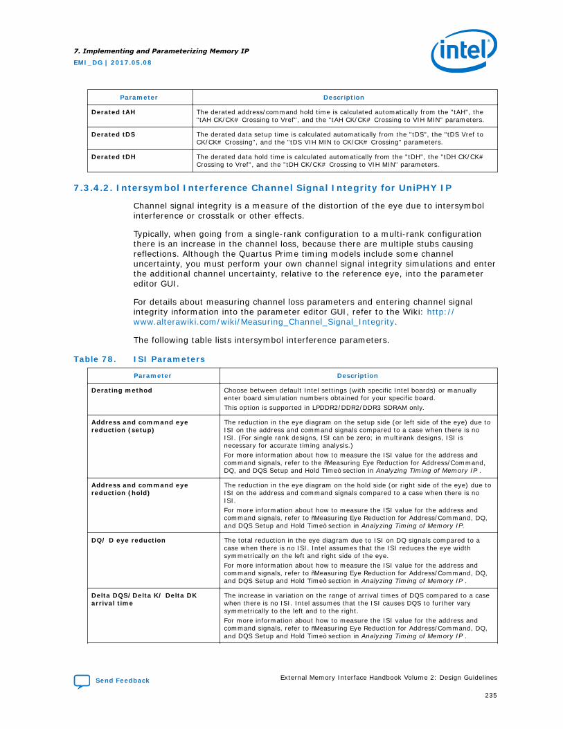
Parameter Description
Derated tAH The derated address/command hold time is calculated automatically from the "tAH", the"tAH CK/CK# Crossing to Vref", and the "tAH CK/CK# Crossing to VIH MIN" parameters.
Derated tDS The derated data setup time is calculated automatically from the "tDS", the "tDS Vref toCK/CK# Crossing", and the "tDS VIH MIN to CK/CK# Crossing" parameters.
Derated tDH The derated data hold time is calculated automatically from the "tDH", the "tDH CK/CK#Crossing to Vref", and the "tDH CK/CK# Crossing to VIH MIN" parameters.
7.3.4.2. Intersymbol Interference Channel Signal Integrity for UniPHY IP
Channel signal integrity is a measure of the distortion of the eye due to intersymbolinterference or crosstalk or other effects.
Typically, when going from a single-rank configuration to a multi-rank configurationthere is an increase in the channel loss, because there are multiple stubs causingreflections. Although the Quartus Prime timing models include some channeluncertainty, you must perform your own channel signal integrity simulations and enterthe additional channel uncertainty, relative to the reference eye, into the parametereditor GUI.
For details about measuring channel loss parameters and entering channel signalintegrity information into the parameter editor GUI, refer to the Wiki: http://www.alterawiki.com/wiki/Measuring_Channel_Signal_Integrity.
The following table lists intersymbol interference parameters.
Table 78. ISI Parameters
Parameter Description
Derating method Choose between default Intel settings (with specific Intel boards) or manuallyenter board simulation numbers obtained for your specific board.This option is supported in LPDDR2/DDR2/DDR3 SDRAM only.
Address and command eyereduction (setup)
The reduction in the eye diagram on the setup side (or left side of the eye) due toISI on the address and command signals compared to a case when there is noISI. (For single rank designs, ISI can be zero; in multirank designs, ISI isnecessary for accurate timing analysis.)For more information about how to measure the ISI value for the address andcommand signals, refer to the “Measuring Eye Reduction for Address/Command,DQ, and DQS Setup and Hold Time” section in Analyzing Timing of Memory IP .
Address and command eyereduction (hold)
The reduction in the eye diagram on the hold side (or right side of the eye) due toISI on the address and command signals compared to a case when there is noISI.For more information about how to measure the ISI value for the address andcommand signals, refer to “Measuring Eye Reduction for Address/Command, DQ,and DQS Setup and Hold Time” section in Analyzing Timing of Memory IP.
DQ/ D eye reduction The total reduction in the eye diagram due to ISI on DQ signals compared to acase when there is no ISI. Intel assumes that the ISI reduces the eye widthsymmetrically on the left and right side of the eye.For more information about how to measure the ISI value for the address andcommand signals, refer to “Measuring Eye Reduction for Address/Command, DQ,and DQS Setup and Hold Time” section in Analyzing Timing of Memory IP .
Delta DQS/Delta K/ Delta DKarrival time
The increase in variation on the range of arrival times of DQS compared to a casewhen there is no ISI. Intel assumes that the ISI causes DQS to further varysymmetrically to the left and to the right.For more information about how to measure the ISI value for the address andcommand signals, refer to “Measuring Eye Reduction for Address/Command, DQ,and DQS Setup and Hold Time” section in Analyzing Timing of Memory IP .
7. Implementing and Parameterizing Memory IP
EMI_DG | 2017.05.08
Send Feedback External Memory Interface Handbook Volume 2: Design Guidelines
235
7.3.4.3. Board Skews for UniPHY IP
PCB traces can have skews between them that can reduce timing margins.Furthermore, skews between different chip selects can further reduce the timingmargin in multiple chip-select topologies.
The Board Skews section of the parameter editor allows you to enter parameters tocompensate for these variations.
Note: You must ensure the timing margin reported in TimeQuest Report DDR is positivewhen the board skew parameters are correct for the PCB.
The following tables list the board skew parameters. For parameter equationscontaining delay values, delays should be measured as follows:
• Non-fly-by topology (Balanced Tree)
— For discrete devices–all the delay (CK, Addr/Cmd, DQ and DQS) from theFPGA are right to every memory device
— For UDIMMs–all the delay (CK, Addr/Cmd, DQ and DQS) from the FPGA toUDIMM connector for every memory device on the UDIMM. If UDIMM delayinformation is available, calculate delays to every memory device on theUDIMM.
— For RDIMMs–the Addr/Cmd and CK delay are from the FPGA to the register onthe RDIMM. The DQ and DQS delay are from FPGA to RDIMM connector forevery memory device on the RDIMM.
— For LRDIMMS–the delay from the FPGA to the register on the LRDIMM.
• Fly-by topology
— For discrete devices–the Addr/Cmd and CK delay are from the FPGA to thefirst memory device. The DQ and DQS delay are from FPGA to every memorydevice.
— For UDIMMs–the Addr/Cmd and CK delay are from the FPGA to the UDIMMconnector. The DQ and DQS delay are from the FPGA to UDIMM connector forevery memory device on the UDIMM.
— For RDIMMs–the Addr/Cmd and CK delay are from the FPGA to the register onthe RDIMM. The DQ and DQS delay are from FPGA to RDIMM connector forevery memory device on the RDIMM.
— For LRDIMMS–the delay from the FPGA to the buffer on the LRDIMM.
Equations apply to any given memory device, except when marked by the board orgroup qualifiers (_b or _g), where they apply to the particular device or group beingiterated over.
Use the Board Skew Parameter Tool to help you calculate the board skews.
Related Information
Board Skew Parameter Tool
7.3.4.3.1. Board Skew Parameters for LPDDR2/DDR2/DDR3 SDRAM
The following table lists board skew parameters for LPDDR2, DDR2, and DDR3interfaces.
7. Implementing and Parameterizing Memory IP
EMI_DG | 2017.05.08
External Memory Interface Handbook Volume 2: Design Guidelines Send Feedback
236
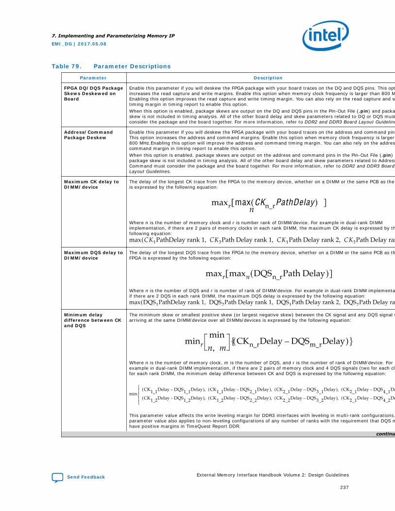
Table 79. Parameter Descriptions
Parameter Description
FPGA DQ/DQS PackageSkews Deskewed onBoard
Enable this parameter if you will deskew the FPGA package with your board traces on the DQ and DQS pins. This optionincreases the read capture and write margins. Enable this option when memory clock frequency is larger than 800 MHz.Enabling this option improves the read capture and write timing margin. You can also rely on the read capture and writetiming margin in timing report to enable this option.When this option is enabled, package skews are output on the DQ and DQS pins in the Pin-Out File (.pin) and packageskew is not included in timing analysis. All of the other board delay and skew parameters related to DQ or DQS mustconsider the package and the board together. For more information, refer to DDR2 and DDR3 Board Layout Guidelines .
Address/CommandPackage Deskew
Enable this parameter if you will deskew the FPGA package with your board traces on the address and command pins.This option increases the address and command margins. Enable this option when memory clock frequency is larger than800 MHz.Enabling this option will improve the address and command timing margin. You can also rely on the address andcommand margin in timing report to enable this option.When this option is enabled, package skews are output on the address and command pins in the Pin-Out File (.pin) andpackage skew is not included in timing analysis. All of the other board delay and skew parameters related to Address andCommand must consider the package and the board together. For more information, refer to DDR2 and DDR3 BoardLayout Guidelines.
Maximum CK delay toDIMM/device
The delay of the longest CK trace from the FPGA to the memory device, whether on a DIMM or the same PCB as the FPGAis expressed by the following equation:
Where n is the number of memory clock and r is number rank of DIMM/device. For example in dual-rank DIMMimplementation, if there are 2 pairs of memory clocks in each rank DIMM, the maximum CK delay is expressed by thefollowing equation:
Maximum DQS delay toDIMM/device
The delay of the longest DQS trace from the FPGA to the memory device, whether on a DIMM or the same PCB as theFPGA is expressed by the following equation:
Where n is the number of DQS and r is number of rank of DIMM/device. For example in dual-rank DIMM implementation,if there are 2 DQS in each rank DIMM, the maximum DQS delay is expressed by the following equation:
Minimum delaydifference between CKand DQS
The minimum skew or smallest positive skew (or largest negative skew) between the CK signal and any DQS signal whenarriving at the same DIMM/device over all DIMMs/devices is expressed by the following equation:
Where n is the number of memory clock, m is the number of DQS, and r is the number of rank of DIMM/device. Forexample in dual-rank DIMM implementation, if there are 2 pairs of memory clock and 4 DQS signals (two for each clock)for each rank DIMM, the minimum delay difference between CK and DQS is expressed by the following equation:
This parameter value affects the write leveling margin for DDR3 interfaces with leveling in multi-rank configurations. Thisparameter value also applies to non-leveling configurations of any number of ranks with the requirement that DQS musthave positive margins in TimeQuest Report DDR.
continued...
7. Implementing and Parameterizing Memory IP
EMI_DG | 2017.05.08
Send Feedback External Memory Interface Handbook Volume 2: Design Guidelines
237
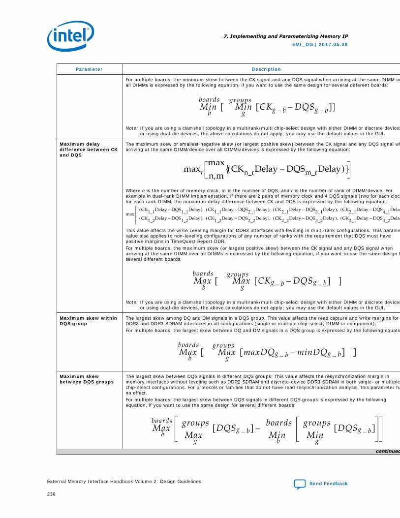
Parameter Description
For multiple boards, the minimum skew between the CK signal and any DQS signal when arriving at the same DIMM overall DIMMs is expressed by the following equation, if you want to use the same design for several different boards:
Note: If you are using a clamshell topology in a multirank/multi chip-select design with either DIMM or discrete devices,
or using dual-die devices, the above calculations do not apply; you may use the default values in the GUI.
Maximum delaydifference between CKand DQS
The maximum skew or smallest negative skew (or largest positive skew) between the CK signal and any DQS signal whenarriving at the same DIMM/device over all DIMMs/devices is expressed by the following equation:
Where n is the number of memory clock, m is the number of DQS, and r is the number of rank of DIMM/device. Forexample in dual-rank DIMM implementation, if there are 2 pairs of memory clock and 4 DQS signals (two for each clock)for each rank DIMM, the maximum delay difference between CK and DQS is expressed by the following equation:
This value affects the write Leveling margin for DDR3 interfaces with leveling in multi-rank configurations. This parametervalue also applies to non-leveling configurations of any number of ranks with the requirement that DQS must havepositive margins in TimeQuest Report DDR.For multiple boards, the maximum skew (or largest positive skew) between the CK signal and any DQS signal whenarriving at the same DIMM over all DIMMs is expressed by the following equation, if you want to use the same design forseveral different boards:
Note: If you are using a clamshell topology in a multirank/multi chip-select design with either DIMM or discrete devices,
or using dual-die devices, the above calculations do not apply; you may use the default values in the GUI.
Maximum skew withinDQS group
The largest skew among DQ and DM signals in a DQS group. This value affects the read capture and write margins forDDR2 and DDR3 SDRAM interfaces in all configurations (single or multiple chip-select, DIMM or component).For multiple boards, the largest skew between DQ and DM signals in a DQS group is expressed by the following equation:
Maximum skewbetween DQS groups
The largest skew between DQS signals in different DQS groups. This value affects the resynchronization margin inmemory interfaces without leveling such as DDR2 SDRAM and discrete-device DDR3 SDRAM in both single- or multiplechip-select configurations. For protocols or families that do not have read resynchronization analysis, this parameter hasno effect.For multiple boards, the largest skew between DQS signals in different DQS groups is expressed by the followingequation, if you want to use the same design for several different boards:
continued...
7. Implementing and Parameterizing Memory IP
EMI_DG | 2017.05.08
External Memory Interface Handbook Volume 2: Design Guidelines Send Feedback
238
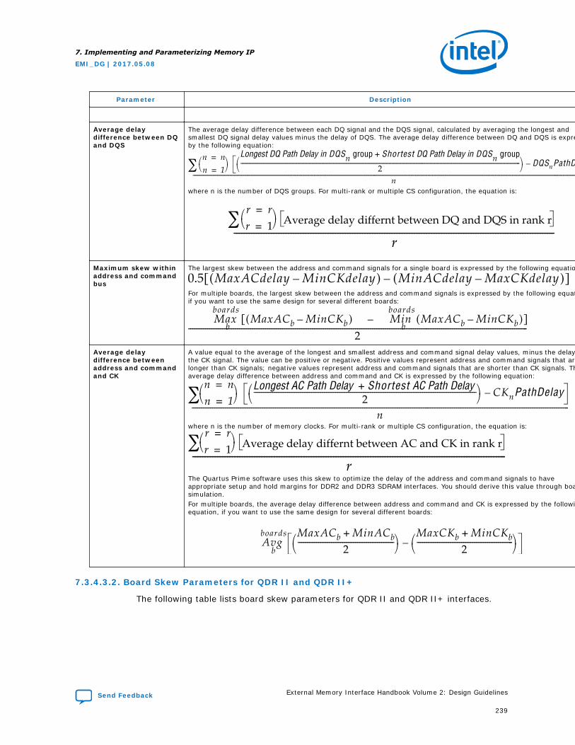
Parameter Description
Average delaydifference between DQand DQS
The average delay difference between each DQ signal and the DQS signal, calculated by averaging the longest andsmallest DQ signal delay values minus the delay of DQS. The average delay difference between DQ and DQS is expressedby the following equation:
where n is the number of DQS groups. For multi-rank or multiple CS configuration, the equation is:
Maximum skew withinaddress and commandbus
The largest skew between the address and command signals for a single board is expressed by the following equation:
For multiple boards, the largest skew between the address and command signals is expressed by the following equation,if you want to use the same design for several different boards:
Average delaydifference betweenaddress and commandand CK
A value equal to the average of the longest and smallest address and command signal delay values, minus the delay ofthe CK signal. The value can be positive or negative. Positive values represent address and command signals that arelonger than CK signals; negative values represent address and command signals that are shorter than CK signals. Theaverage delay difference between address and command and CK is expressed by the following equation:
where n is the number of memory clocks. For multi-rank or multiple CS configuration, the equation is:
The Quartus Prime software uses this skew to optimize the delay of the address and command signals to haveappropriate setup and hold margins for DDR2 and DDR3 SDRAM interfaces. You should derive this value through boardsimulation.For multiple boards, the average delay difference between address and command and CK is expressed by the followingequation, if you want to use the same design for several different boards:
7.3.4.3.2. Board Skew Parameters for QDR II and QDR II+
The following table lists board skew parameters for QDR II and QDR II+ interfaces.
7. Implementing and Parameterizing Memory IP
EMI_DG | 2017.05.08
Send Feedback External Memory Interface Handbook Volume 2: Design Guidelines
239
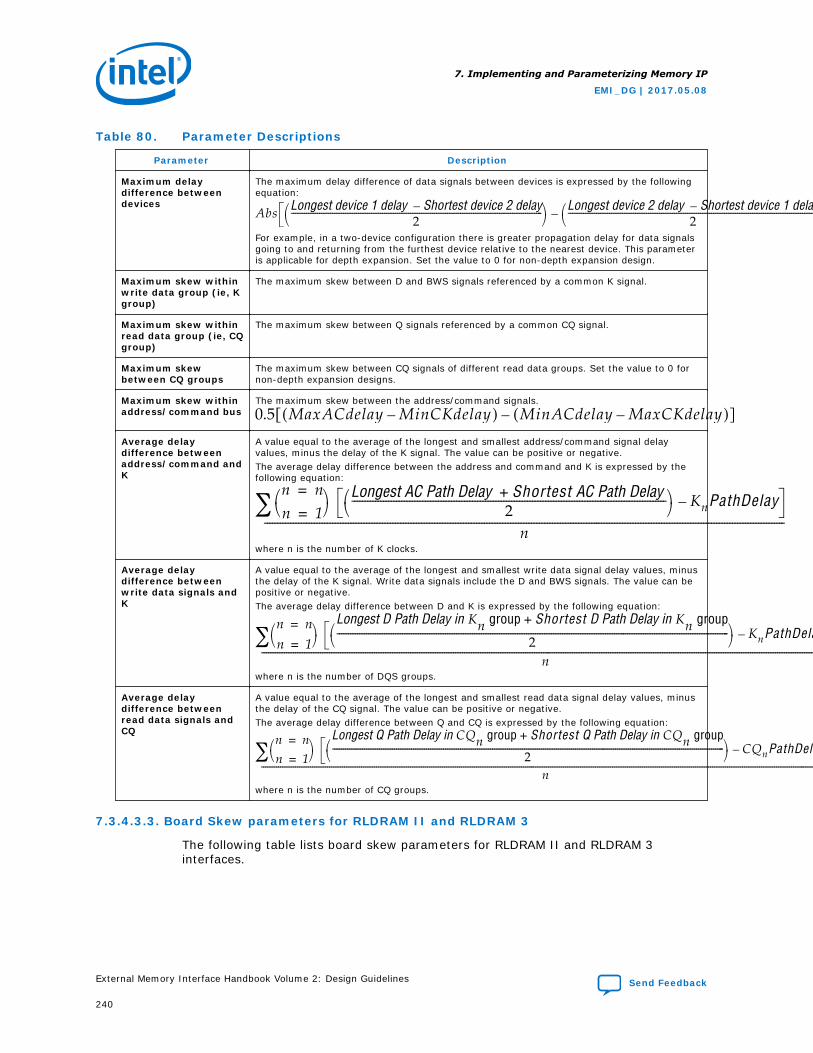
Table 80. Parameter Descriptions
Parameter Description
Maximum delaydifference betweendevices
The maximum delay difference of data signals between devices is expressed by the followingequation:
For example, in a two-device configuration there is greater propagation delay for data signalsgoing to and returning from the furthest device relative to the nearest device. This parameteris applicable for depth expansion. Set the value to 0 for non-depth expansion design.
Maximum skew withinwrite data group (ie, Kgroup)
The maximum skew between D and BWS signals referenced by a common K signal.
Maximum skew withinread data group (ie, CQgroup)
The maximum skew between Q signals referenced by a common CQ signal.
Maximum skewbetween CQ groups
The maximum skew between CQ signals of different read data groups. Set the value to 0 fornon-depth expansion designs.
Maximum skew withinaddress/command bus
The maximum skew between the address/command signals.
Average delaydifference betweenaddress/command andK
A value equal to the average of the longest and smallest address/command signal delayvalues, minus the delay of the K signal. The value can be positive or negative.The average delay difference between the address and command and K is expressed by thefollowing equation:
where n is the number of K clocks.
Average delaydifference betweenwrite data signals andK
A value equal to the average of the longest and smallest write data signal delay values, minusthe delay of the K signal. Write data signals include the D and BWS signals. The value can bepositive or negative.The average delay difference between D and K is expressed by the following equation:
where n is the number of DQS groups.
Average delaydifference betweenread data signals andCQ
A value equal to the average of the longest and smallest read data signal delay values, minusthe delay of the CQ signal. The value can be positive or negative.The average delay difference between Q and CQ is expressed by the following equation:
where n is the number of CQ groups.
7.3.4.3.3. Board Skew parameters for RLDRAM II and RLDRAM 3
The following table lists board skew parameters for RLDRAM II and RLDRAM 3interfaces.
7. Implementing and Parameterizing Memory IP
EMI_DG | 2017.05.08
External Memory Interface Handbook Volume 2: Design Guidelines Send Feedback
240
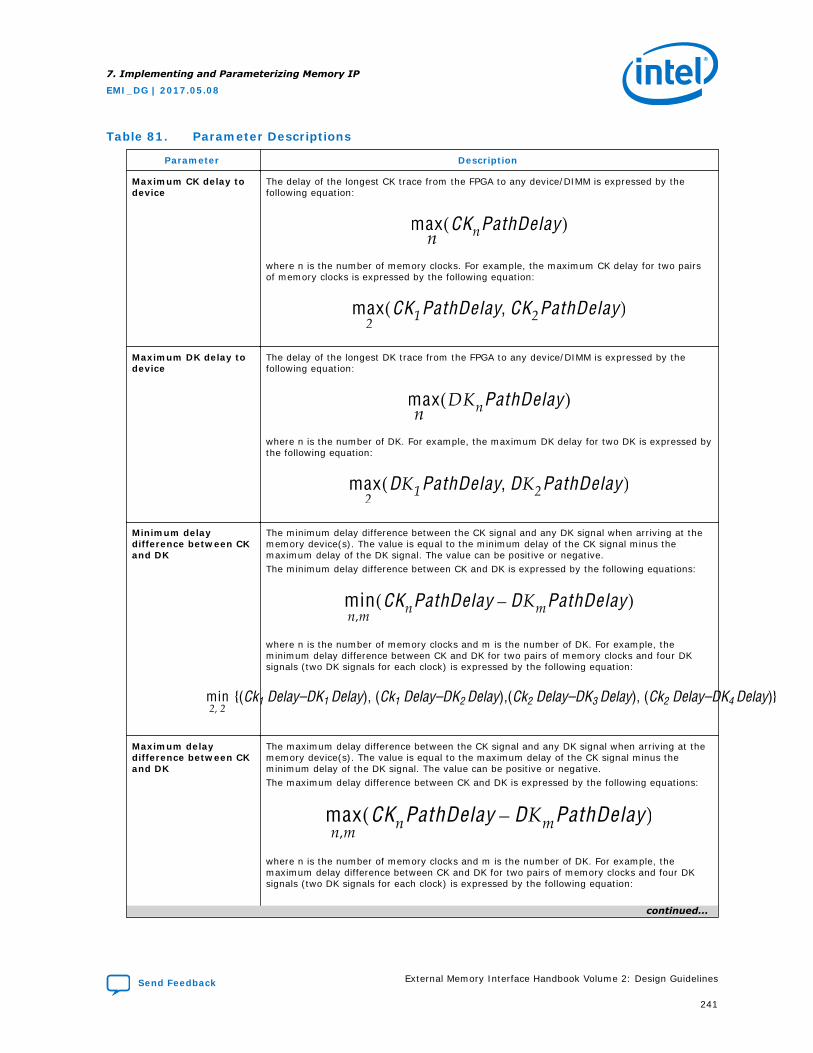
Table 81. Parameter Descriptions
Parameter Description
Maximum CK delay todevice
The delay of the longest CK trace from the FPGA to any device/DIMM is expressed by thefollowing equation:
where n is the number of memory clocks. For example, the maximum CK delay for two pairsof memory clocks is expressed by the following equation:
Maximum DK delay todevice
The delay of the longest DK trace from the FPGA to any device/DIMM is expressed by thefollowing equation:
where n is the number of DK. For example, the maximum DK delay for two DK is expressed bythe following equation:
Minimum delaydifference between CKand DK
The minimum delay difference between the CK signal and any DK signal when arriving at thememory device(s). The value is equal to the minimum delay of the CK signal minus themaximum delay of the DK signal. The value can be positive or negative.The minimum delay difference between CK and DK is expressed by the following equations:
where n is the number of memory clocks and m is the number of DK. For example, theminimum delay difference between CK and DK for two pairs of memory clocks and four DKsignals (two DK signals for each clock) is expressed by the following equation:
Maximum delaydifference between CKand DK
The maximum delay difference between the CK signal and any DK signal when arriving at thememory device(s). The value is equal to the maximum delay of the CK signal minus theminimum delay of the DK signal. The value can be positive or negative.The maximum delay difference between CK and DK is expressed by the following equations:
where n is the number of memory clocks and m is the number of DK. For example, themaximum delay difference between CK and DK for two pairs of memory clocks and four DKsignals (two DK signals for each clock) is expressed by the following equation:
continued...
7. Implementing and Parameterizing Memory IP
EMI_DG | 2017.05.08
Send Feedback External Memory Interface Handbook Volume 2: Design Guidelines
241
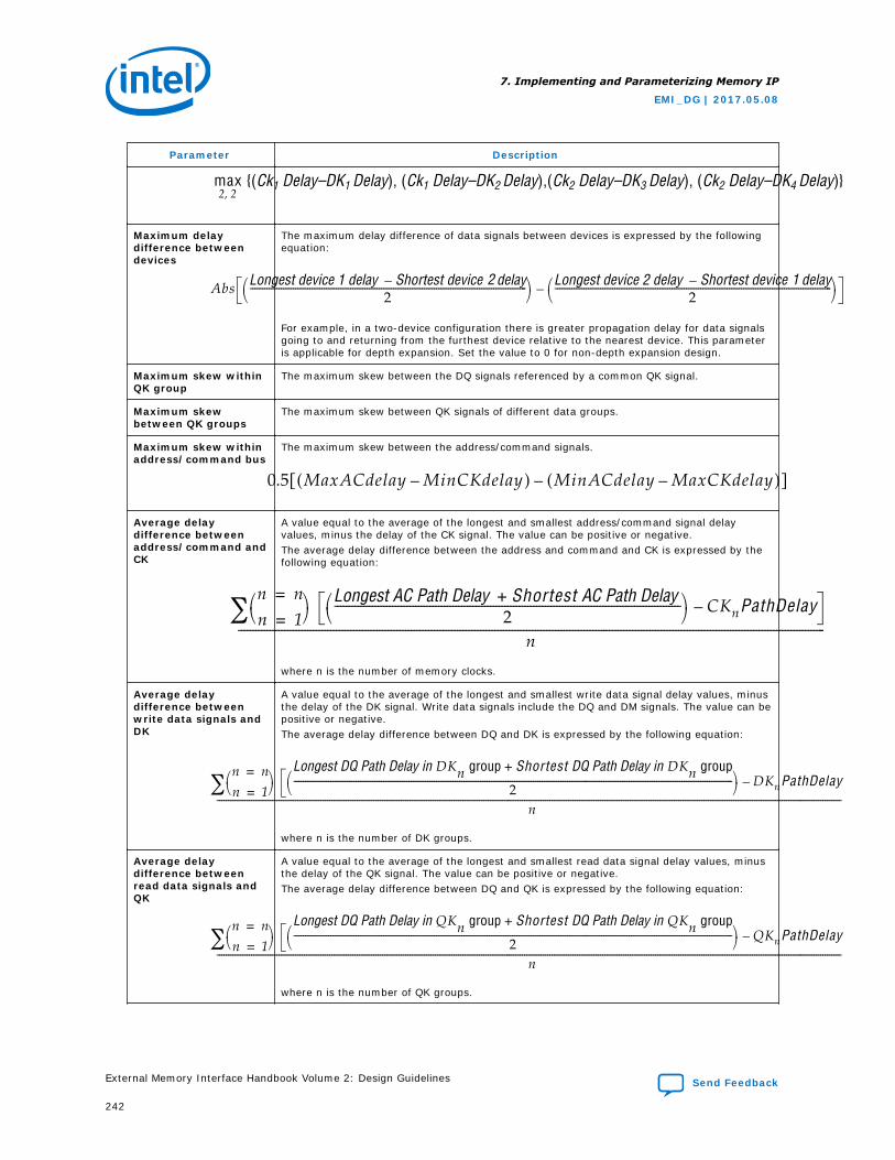
Parameter Description
Maximum delaydifference betweendevices
The maximum delay difference of data signals between devices is expressed by the followingequation:
For example, in a two-device configuration there is greater propagation delay for data signalsgoing to and returning from the furthest device relative to the nearest device. This parameteris applicable for depth expansion. Set the value to 0 for non-depth expansion design.
Maximum skew withinQK group
The maximum skew between the DQ signals referenced by a common QK signal.
Maximum skewbetween QK groups
The maximum skew between QK signals of different data groups.
Maximum skew withinaddress/command bus
The maximum skew between the address/command signals.
Average delaydifference betweenaddress/command andCK
A value equal to the average of the longest and smallest address/command signal delayvalues, minus the delay of the CK signal. The value can be positive or negative.The average delay difference between the address and command and CK is expressed by thefollowing equation:
where n is the number of memory clocks.
Average delaydifference betweenwrite data signals andDK
A value equal to the average of the longest and smallest write data signal delay values, minusthe delay of the DK signal. Write data signals include the DQ and DM signals. The value can bepositive or negative.The average delay difference between DQ and DK is expressed by the following equation:
where n is the number of DK groups.
Average delaydifference betweenread data signals andQK
A value equal to the average of the longest and smallest read data signal delay values, minusthe delay of the QK signal. The value can be positive or negative.The average delay difference between DQ and QK is expressed by the following equation:
where n is the number of QK groups.
7. Implementing and Parameterizing Memory IP
EMI_DG | 2017.05.08
External Memory Interface Handbook Volume 2: Design Guidelines Send Feedback
242
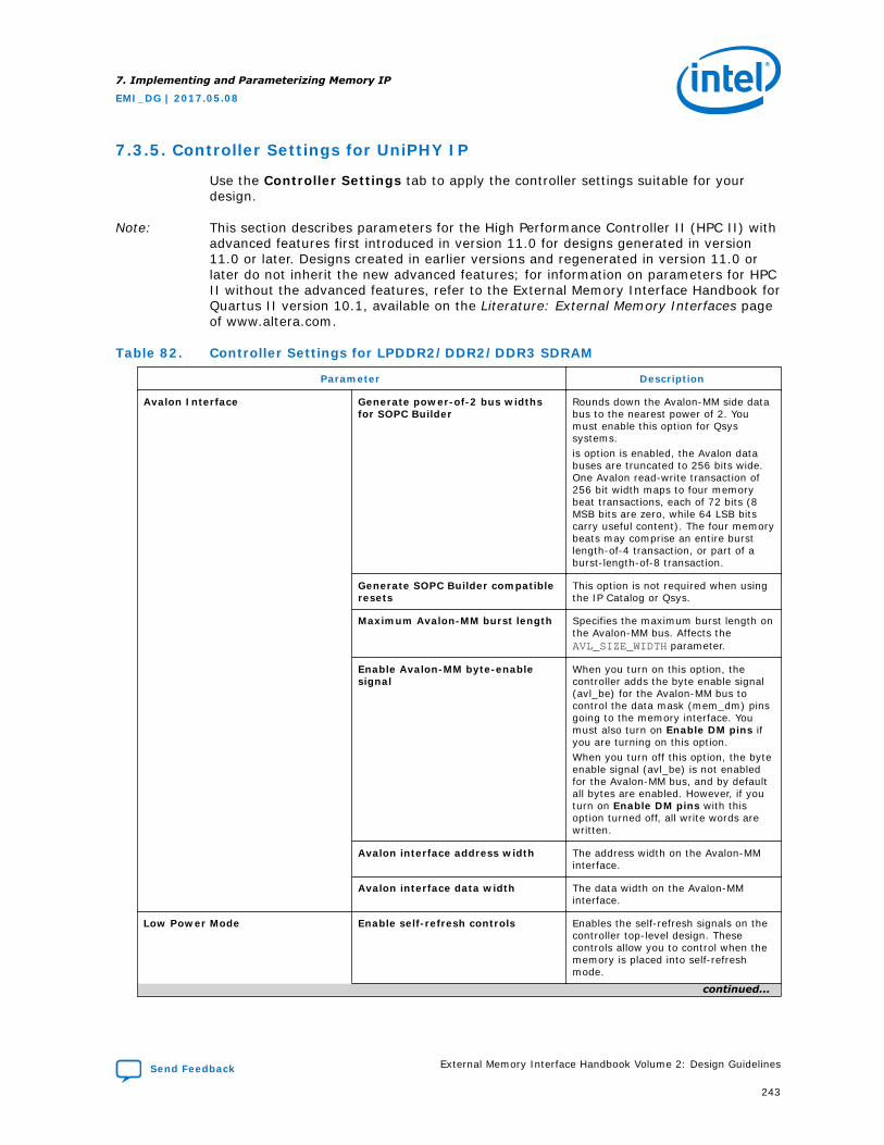
7.3.5. Controller Settings for UniPHY IP
Use the Controller Settings tab to apply the controller settings suitable for yourdesign.
Note: This section describes parameters for the High Performance Controller II (HPC II) withadvanced features first introduced in version 11.0 for designs generated in version11.0 or later. Designs created in earlier versions and regenerated in version 11.0 orlater do not inherit the new advanced features; for information on parameters for HPCII without the advanced features, refer to the External Memory Interface Handbook forQuartus II version 10.1, available on the Literature: External Memory Interfaces pageof www.altera.com.
Table 82. Controller Settings for LPDDR2/DDR2/DDR3 SDRAM
Parameter Description
Avalon Interface Generate power-of-2 bus widthsfor SOPC Builder
Rounds down the Avalon-MM side databus to the nearest power of 2. Youmust enable this option for Qsyssystems.is option is enabled, the Avalon databuses are truncated to 256 bits wide.One Avalon read-write transaction of256 bit width maps to four memorybeat transactions, each of 72 bits (8MSB bits are zero, while 64 LSB bitscarry useful content). The four memorybeats may comprise an entire burstlength-of-4 transaction, or part of aburst-length-of-8 transaction.
Generate SOPC Builder compatibleresets
This option is not required when usingthe IP Catalog or Qsys.
Maximum Avalon-MM burst length Specifies the maximum burst length onthe Avalon-MM bus. Affects theAVL_SIZE_WIDTH parameter.
Enable Avalon-MM byte-enablesignal
When you turn on this option, thecontroller adds the byte enable signal(avl_be) for the Avalon-MM bus tocontrol the data mask (mem_dm) pinsgoing to the memory interface. Youmust also turn on Enable DM pins ifyou are turning on this option.When you turn off this option, the byteenable signal (avl_be) is not enabledfor the Avalon-MM bus, and by defaultall bytes are enabled. However, if youturn on Enable DM pins with thisoption turned off, all write words arewritten.
Avalon interface address width The address width on the Avalon-MMinterface.
Avalon interface data width The data width on the Avalon-MMinterface.
Low Power Mode Enable self-refresh controls Enables the self-refresh signals on thecontroller top-level design. Thesecontrols allow you to control when thememory is placed into self-refreshmode.
continued...
7. Implementing and Parameterizing Memory IP
EMI_DG | 2017.05.08
Send Feedback External Memory Interface Handbook Volume 2: Design Guidelines
243
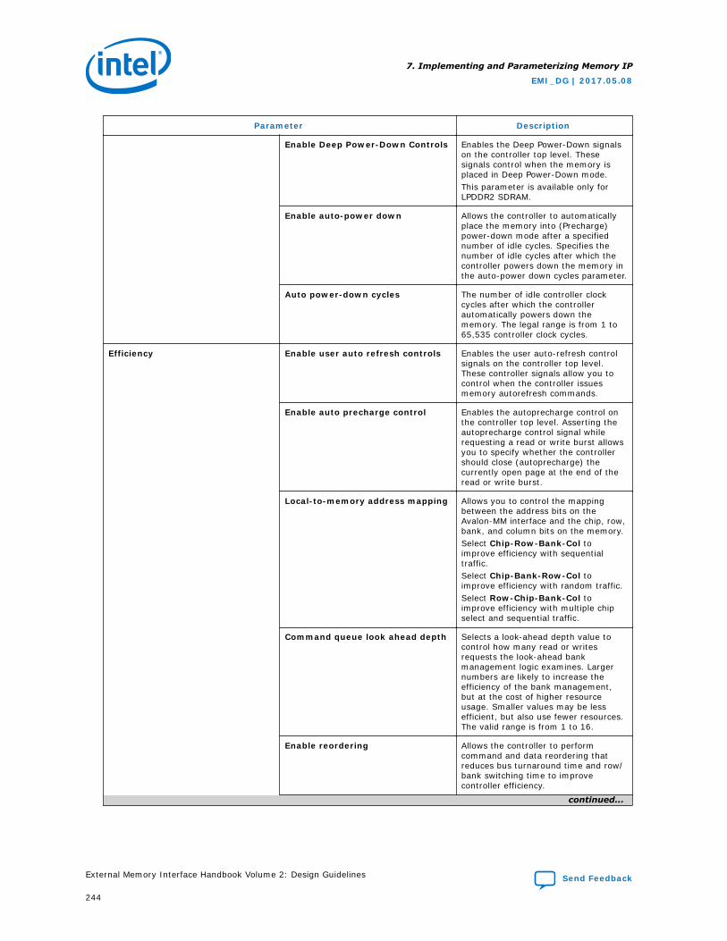
Parameter Description
Enable Deep Power-Down Controls Enables the Deep Power-Down signalson the controller top level. Thesesignals control when the memory isplaced in Deep Power-Down mode.This parameter is available only forLPDDR2 SDRAM.
Enable auto-power down Allows the controller to automaticallyplace the memory into (Precharge)power-down mode after a specifiednumber of idle cycles. Specifies thenumber of idle cycles after which thecontroller powers down the memory inthe auto-power down cycles parameter.
Auto power-down cycles The number of idle controller clockcycles after which the controllerautomatically powers down thememory. The legal range is from 1 to65,535 controller clock cycles.
Efficiency Enable user auto refresh controls Enables the user auto-refresh controlsignals on the controller top level.These controller signals allow you tocontrol when the controller issuesmemory autorefresh commands.
Enable auto precharge control Enables the autoprecharge control onthe controller top level. Asserting theautoprecharge control signal whilerequesting a read or write burst allowsyou to specify whether the controllershould close (autoprecharge) thecurrently open page at the end of theread or write burst.
Local-to-memory address mapping Allows you to control the mappingbetween the address bits on theAvalon-MM interface and the chip, row,bank, and column bits on the memory.Select Chip-Row-Bank-Col toimprove efficiency with sequentialtraffic.Select Chip-Bank-Row-Col toimprove efficiency with random traffic.Select Row-Chip-Bank-Col toimprove efficiency with multiple chipselect and sequential traffic.
Command queue look ahead depth Selects a look-ahead depth value tocontrol how many read or writesrequests the look-ahead bankmanagement logic examines. Largernumbers are likely to increase theefficiency of the bank management,but at the cost of higher resourceusage. Smaller values may be lessefficient, but also use fewer resources.The valid range is from 1 to 16.
Enable reordering Allows the controller to performcommand and data reordering thatreduces bus turnaround time and row/bank switching time to improvecontroller efficiency.
continued...
7. Implementing and Parameterizing Memory IP
EMI_DG | 2017.05.08
External Memory Interface Handbook Volume 2: Design Guidelines Send Feedback
244
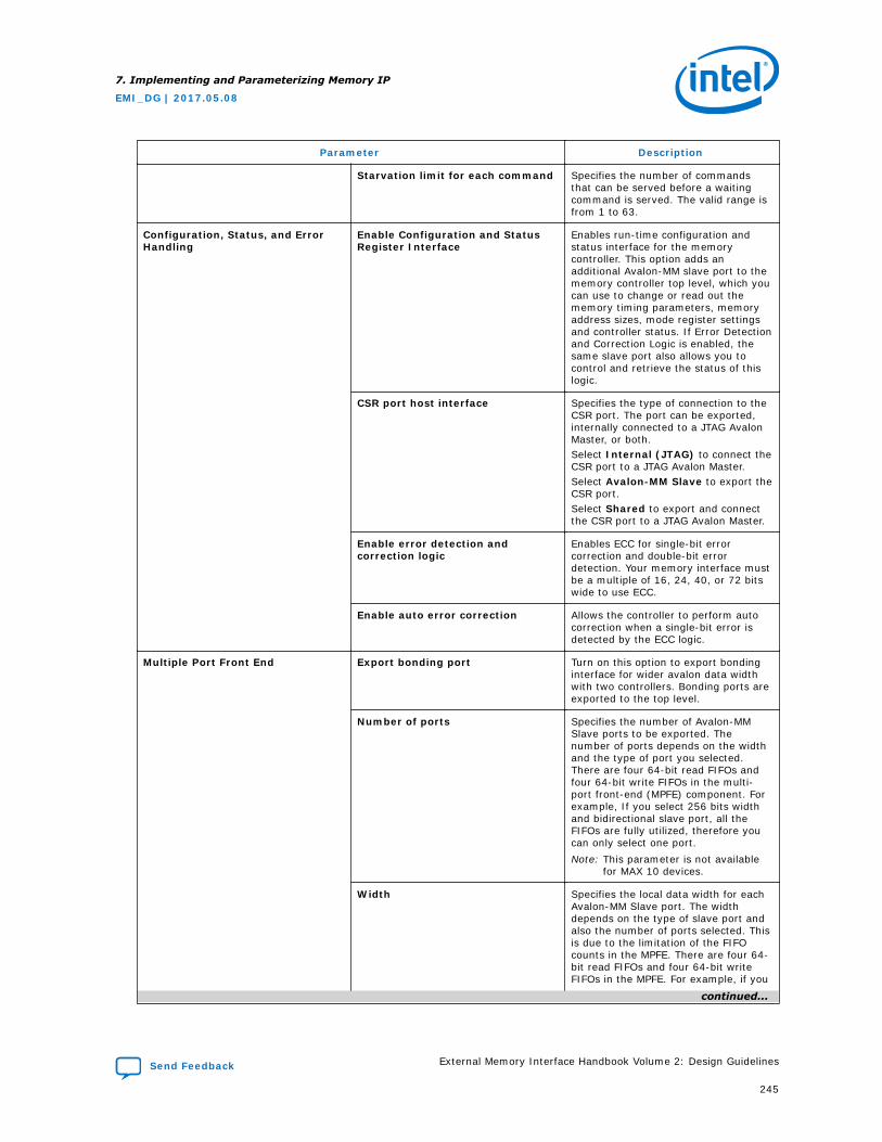
Parameter Description
Starvation limit for each command Specifies the number of commandsthat can be served before a waitingcommand is served. The valid range isfrom 1 to 63.
Configuration, Status, and ErrorHandling
Enable Configuration and StatusRegister Interface
Enables run-time configuration andstatus interface for the memorycontroller. This option adds anadditional Avalon-MM slave port to thememory controller top level, which youcan use to change or read out thememory timing parameters, memoryaddress sizes, mode register settingsand controller status. If Error Detectionand Correction Logic is enabled, thesame slave port also allows you tocontrol and retrieve the status of thislogic.
CSR port host interface Specifies the type of connection to theCSR port. The port can be exported,internally connected to a JTAG AvalonMaster, or both.Select Internal (JTAG) to connect theCSR port to a JTAG Avalon Master.Select Avalon-MM Slave to export theCSR port.Select Shared to export and connectthe CSR port to a JTAG Avalon Master.
Enable error detection andcorrection logic
Enables ECC for single-bit errorcorrection and double-bit errordetection. Your memory interface mustbe a multiple of 16, 24, 40, or 72 bitswide to use ECC.
Enable auto error correction Allows the controller to perform autocorrection when a single-bit error isdetected by the ECC logic.
Multiple Port Front End Export bonding port Turn on this option to export bondinginterface for wider avalon data widthwith two controllers. Bonding ports areexported to the top level.
Number of ports Specifies the number of Avalon-MMSlave ports to be exported. Thenumber of ports depends on the widthand the type of port you selected.There are four 64-bit read FIFOs andfour 64-bit write FIFOs in the multi-port front-end (MPFE) component. Forexample, If you select 256 bits widthand bidirectional slave port, all theFIFOs are fully utilized, therefore youcan only select one port.Note: This parameter is not available
for MAX 10 devices.
Width Specifies the local data width for eachAvalon-MM Slave port. The widthdepends on the type of slave port andalso the number of ports selected. Thisis due to the limitation of the FIFOcounts in the MPFE. There are four 64-bit read FIFOs and four 64-bit writeFIFOs in the MPFE. For example, if you
continued...
7. Implementing and Parameterizing Memory IP
EMI_DG | 2017.05.08
Send Feedback External Memory Interface Handbook Volume 2: Design Guidelines
245
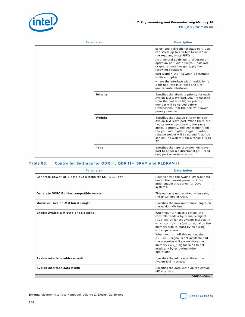
Parameter Description
select one bidirectional slave port, youcan select up to 256 bits to utilize allthe read and write FIFOs.As a general guideline to choosing anoptimum port width for your half-rateor quarter-rate design, apply thefollowing equation:port width = 2 x DQ width x Interfacewidth multiplierwhere the interface width multiplier is2 for half-rate interfaces and 4 forquarter-rate interfaces.
Priority Specifies the absolute priority for eachAvalon-MM Slave port. Any transactionfrom the port with higher prioritynumber will be served beforetransactions from the port with lowerpriority number.
Weight Specifies the relative priority for eachAvalon-MM Slave port. When there aretwo or more ports having the sameabsolute priority, the transaction fromthe port with higher (bigger number)relative weight will be served first. Youcan set the weight from a range of 0 to32.
Type Specifies the type of Avalon MM slaveport to either a bidirectional port, readonly port or write only port.
Table 83. Controller Settings for QDR II/QDR II+ SRAM and RLDRAM II
Parameter Description
Generate power-of-2 data bus widths for SOPC Builder Rounds down the Avalon-MM side databus to the nearest power of 2. Youmust enable this option for Qsyssystems.
Generate SOPC Builder compatible resets This option is not required when usingthe IP Catalog or Qsys.
Maximum Avalon-MM burst length Specifies the maximum burst length onthe Avalon-MM bus.
Enable Avalon-MM byte-enable signal When you turn on this option, thecontroller adds a byte-enable signal(avl_be_w) for the Avalon-MM bus, inwhich controls the bws_n signal on thememory side to mask bytes duringwrite operations.When you turn off this option, theavl_be_w signal is not available andthe controller will always drive thememory bws_n signal so as to notmask any bytes during writeoperations.
Avalon interface address width Specifies the address width on theAvalon-MM interface.
Avalon interface data width Specifies the data width on the Avalon-MM interface.
continued...
7. Implementing and Parameterizing Memory IP
EMI_DG | 2017.05.08
External Memory Interface Handbook Volume 2: Design Guidelines Send Feedback
246
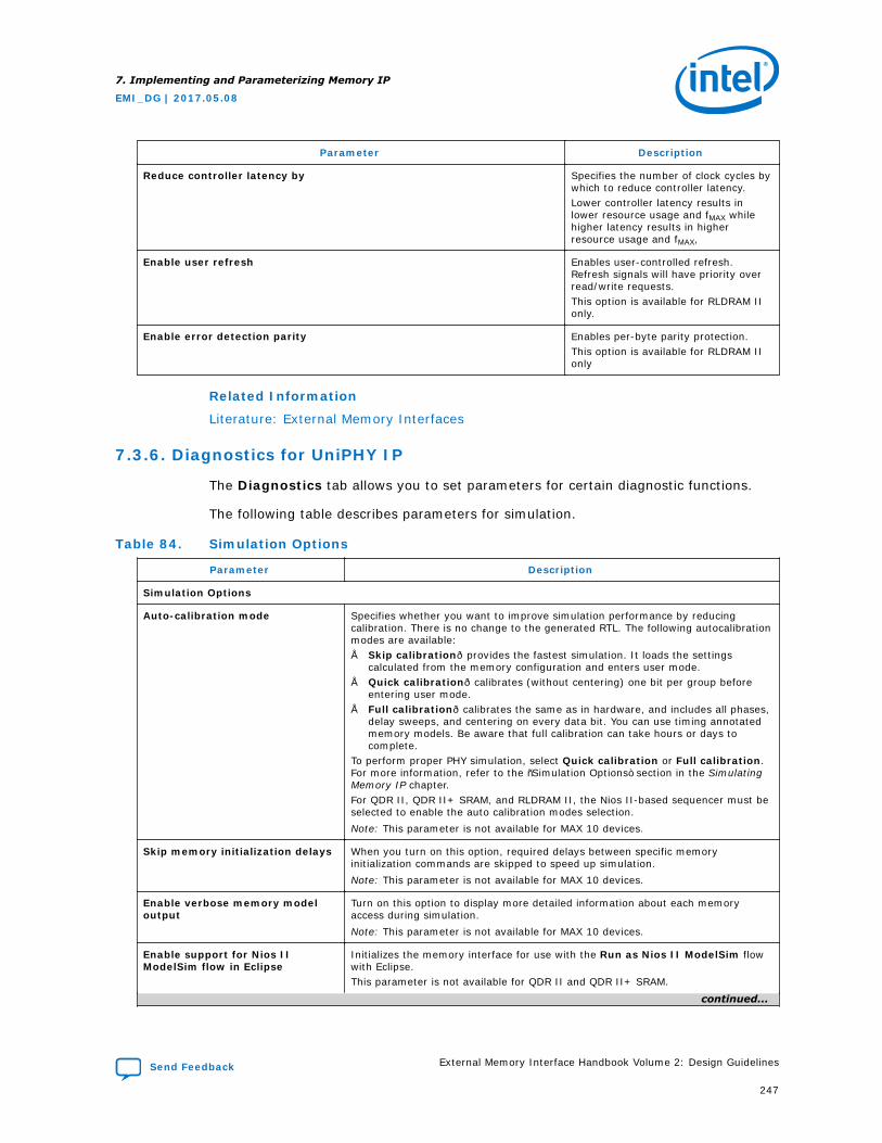
Parameter Description
Reduce controller latency by Specifies the number of clock cycles bywhich to reduce controller latency.Lower controller latency results inlower resource usage and fMAX whilehigher latency results in higherresource usage and fMAX,
Enable user refresh Enables user-controlled refresh.Refresh signals will have priority overread/write requests.This option is available for RLDRAM IIonly.
Enable error detection parity Enables per-byte parity protection.This option is available for RLDRAM IIonly
Related Information
Literature: External Memory Interfaces
7.3.6. Diagnostics for UniPHY IP
The Diagnostics tab allows you to set parameters for certain diagnostic functions.
The following table describes parameters for simulation.
Table 84. Simulation Options
Parameter Description
Simulation Options
Auto-calibration mode Specifies whether you want to improve simulation performance by reducingcalibration. There is no change to the generated RTL. The following autocalibrationmodes are available:• Skip calibration—provides the fastest simulation. It loads the settings
calculated from the memory configuration and enters user mode.• Quick calibration—calibrates (without centering) one bit per group before
entering user mode.• Full calibration—calibrates the same as in hardware, and includes all phases,
delay sweeps, and centering on every data bit. You can use timing annotatedmemory models. Be aware that full calibration can take hours or days tocomplete.
To perform proper PHY simulation, select Quick calibration or Full calibration.For more information, refer to the “Simulation Options” section in the SimulatingMemory IP chapter.For QDR II, QDR II+ SRAM, and RLDRAM II, the Nios II-based sequencer must beselected to enable the auto calibration modes selection.Note: This parameter is not available for MAX 10 devices.
Skip memory initialization delays When you turn on this option, required delays between specific memoryinitialization commands are skipped to speed up simulation.Note: This parameter is not available for MAX 10 devices.
Enable verbose memory modeloutput
Turn on this option to display more detailed information about each memoryaccess during simulation.Note: This parameter is not available for MAX 10 devices.
Enable support for Nios IIModelSim flow in Eclipse
Initializes the memory interface for use with the Run as Nios II ModelSim flowwith Eclipse.This parameter is not available for QDR II and QDR II+ SRAM.
continued...
7. Implementing and Parameterizing Memory IP
EMI_DG | 2017.05.08
Send Feedback External Memory Interface Handbook Volume 2: Design Guidelines
247
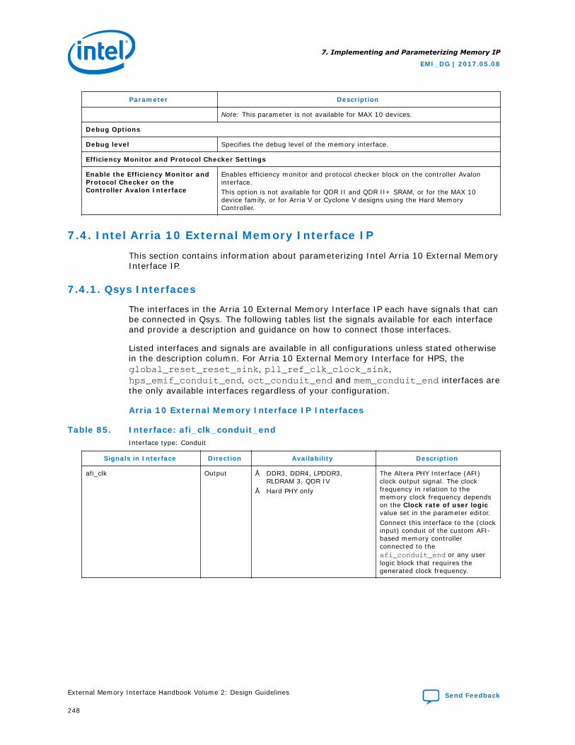
Parameter Description
Note: This parameter is not available for MAX 10 devices.
Debug Options
Debug level Specifies the debug level of the memory interface.
Efficiency Monitor and Protocol Checker Settings
Enable the Efficiency Monitor andProtocol Checker on theController Avalon Interface
Enables efficiency monitor and protocol checker block on the controller Avaloninterface.This option is not available for QDR II and QDR II+ SRAM, or for the MAX 10device family, or for Arria V or Cyclone V designs using the Hard MemoryController.
7.4. Intel Arria 10 External Memory Interface IP
This section contains information about parameterizing Intel Arria 10 External MemoryInterface IP.
7.4.1. Qsys Interfaces
The interfaces in the Arria 10 External Memory Interface IP each have signals that canbe connected in Qsys. The following tables list the signals available for each interfaceand provide a description and guidance on how to connect those interfaces.
Listed interfaces and signals are available in all configurations unless stated otherwisein the description column. For Arria 10 External Memory Interface for HPS, theglobal_reset_reset_sink, pll_ref_clk_clock_sink,hps_emif_conduit_end, oct_conduit_end and mem_conduit_end interfaces arethe only available interfaces regardless of your configuration.
Arria 10 External Memory Interface IP Interfaces
Table 85. Interface: afi_clk_conduit_endInterface type: Conduit
Signals in Interface Direction Availability Description
afi_clk Output • DDR3, DDR4, LPDDR3,RLDRAM 3, QDR IV
• Hard PHY only
The Altera PHY Interface (AFI)clock output signal. The clockfrequency in relation to thememory clock frequency dependson the Clock rate of user logicvalue set in the parameter editor.Connect this interface to the (clockinput) conduit of the custom AFI-based memory controllerconnected to theafi_conduit_end or any userlogic block that requires thegenerated clock frequency.
7. Implementing and Parameterizing Memory IP
EMI_DG | 2017.05.08
External Memory Interface Handbook Volume 2: Design Guidelines Send Feedback
248
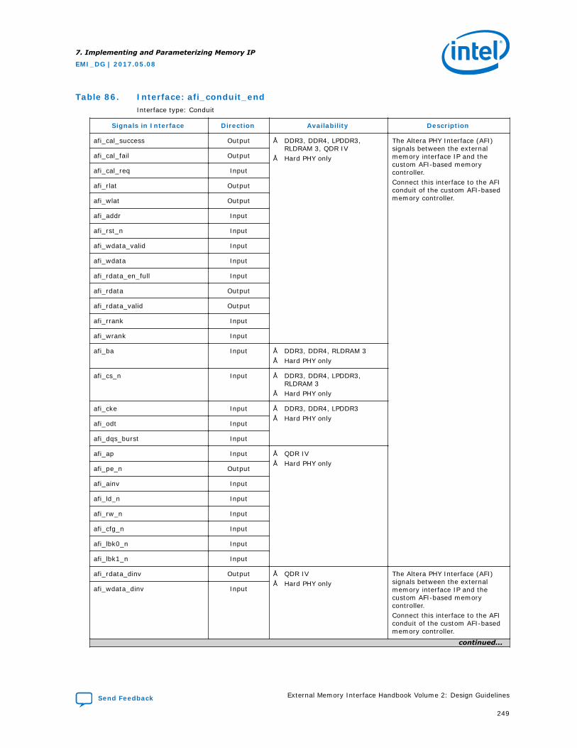
Table 86. Interface: afi_conduit_endInterface type: Conduit
Signals in Interface Direction Availability Description
afi_cal_success Output • DDR3, DDR4, LPDDR3,RLDRAM 3, QDR IV
• Hard PHY only
The Altera PHY Interface (AFI)signals between the externalmemory interface IP and thecustom AFI-based memorycontroller.Connect this interface to the AFIconduit of the custom AFI-basedmemory controller.
afi_cal_fail Output
afi_cal_req Input
afi_rlat Output
afi_wlat Output
afi_addr Input
afi_rst_n Input
afi_wdata_valid Input
afi_wdata Input
afi_rdata_en_full Input
afi_rdata Output
afi_rdata_valid Output
afi_rrank Input
afi_wrank Input
afi_ba Input • DDR3, DDR4, RLDRAM 3• Hard PHY only
afi_cs_n Input • DDR3, DDR4, LPDDR3,RLDRAM 3
• Hard PHY only
afi_cke Input • DDR3, DDR4, LPDDR3• Hard PHY only
afi_odt Input
afi_dqs_burst Input
afi_ap Input • QDR IV• Hard PHY only
afi_pe_n Output
afi_ainv Input
afi_ld_n Input
afi_rw_n Input
afi_cfg_n Input
afi_lbk0_n Input
afi_lbk1_n Input
afi_rdata_dinv Output • QDR IV• Hard PHY only
The Altera PHY Interface (AFI)signals between the externalmemory interface IP and thecustom AFI-based memorycontroller.Connect this interface to the AFIconduit of the custom AFI-basedmemory controller.
afi_wdata_dinv Input
continued...
7. Implementing and Parameterizing Memory IP
EMI_DG | 2017.05.08
Send Feedback External Memory Interface Handbook Volume 2: Design Guidelines
249
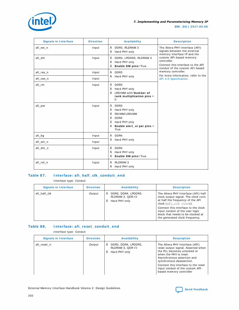
Signals in Interface Direction Availability Description
afi_we_n Input • DDR3, RLDRAM 3• Hard PHY only
The Altera PHY Interface (AFI)signals between the externalmemory interface IP and thecustom AFI-based memorycontroller.Connect this interface to the AFIconduit of the custom AFI-basedmemory controller.For more information, refer to the AFI 4.0 Specification.
afi_dm Input • DDR3, LPDDR3, RLDRAM 3• Hard PHY only• Enable DM pins=True
afi_ras_n Input • DDR3• Hard PHY only
afi_cas_n Input
afi_rm Input • DDR3• Hard PHY only• LRDIMM with Number of
rank multiplication pins >0
afi_par Input • DDR3• Hard PHY only• RDIMM/LRDIMM• DDR4• Hard PHY only• Enable alert_n/par pins =
True
afi_bg Input • DDR4• Hard PHY only
afi_act_n Input
afi_dm_n Input • DDR4• Hard PHY only• Enable DM pins=True
afi_ref_n Input • RLDRAM 3• Hard PHY only
Table 87. Interface: afi_half_clk_conduit_endInterface type: Conduit
Signals in Interface Direction Availability Description
afi_half_clk Output • DDR3, DDR4, LPDDR3,RLDRAM 3, QDR IV
• Hard PHY only
The Altera PHY Interface (AFI) halfclock output signal. The clock runsat half the frequency of the AFIclock (afi_clk clock).Connect this interface to the clockinput conduit of the user logicblock that needs to be clocked atthe generated clock frequency.
Table 88. Interface: afi_reset_conduit_endInterface type: Conduit
Signals in Interface Direction Availability Description
afi_reset_n Output • DDR3, DDR4, LPDDR3,RLDRAM 3, QDR IV
• Hard PHY only
The Altera PHY Interface (AFI)reset output signal. Asserted whenthe PLL becomes unlocked orwhen the PHY is reset.Asynchronous assertion andsynchronous deassertion.Connect this interface to the resetinput conduit of the custom AFI-based memory controller
7. Implementing and Parameterizing Memory IP
EMI_DG | 2017.05.08
External Memory Interface Handbook Volume 2: Design Guidelines Send Feedback
250
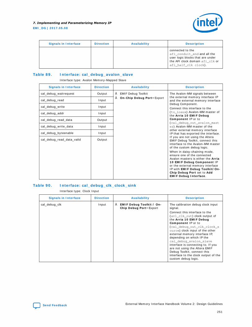
Signals in Interface Direction Availability Description
connected to theafi_conduit_end and all theuser logic blocks that are underthe AFI clock domain afi_clk orafi_half_clk clock).
Table 89. Interface: cal_debug_avalon_slaveInterface type: Avalon Memory-Mapped Slave
Signals in Interface Direction Availability Description
cal_debug_waitrequest Output • EMIF Debug Toolkit• On-Chip Debug Port=Export
The Avalon-MM signals betweenthe external memory interface IPand the external memory interfaceDebug Component.Connect this interface to the(to_ioaux) Avalon-MM master ofthe Arria 10 EMIF DebugComponent IP or to(cal_debug_out_avalon_master) Avalon-MM master of theother external memory interfaceIP that has exported the interface.If you are not using the AlteraEMIF Debug Toolkit, connect thisinterface to the Avalon-MM masterof the custom debug logic.When in daisy-chaining mode,ensure one of the connectedAvalon masters is either the Arria10 EMIF Debug Component IPor the external memory interfaceIP with EMIF Debug Toolkit/On-Chip Debug Port set to AddEMIF Debug Interface.
cal_debug_read Input
cal_debug_write Input
cal_debug_addr Input
cal_debug_read_data Output
cal_debug_write_data Input
cal_debug_byteenable Input
cal_debug_read_data_valid Output
Table 90. Interface: cal_debug_clk_clock_sinkInterface type: Clock Input
Signals in Interface Direction Availability Description
cal_debug_clk Input • EMIF Debug Toolkit / On-Chip Debug Port=Export
The calibration debug clock inputsignal.Connect this interface to the(avl_clk_out) clock output ofthe Arria 10 EMIF DebugComponent IP or to(cal_debug_out_clk_clock_source) clock input of the otherexternal memory interface IP,depending on which IP thecal_debug_avalon_slaveinterface is connecting to. If youare not using the Altera EMIFDebug Toolkit, connect thisinterface to the clock output of thecustom debug logic.
7. Implementing and Parameterizing Memory IP
EMI_DG | 2017.05.08
Send Feedback External Memory Interface Handbook Volume 2: Design Guidelines
251
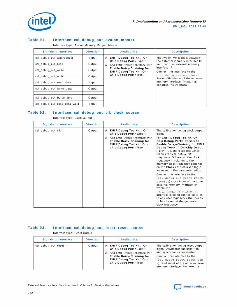
Table 91. Interface: cal_debug_out_avalon_masterInterface type: Avalon Memory-Mapped Master
Signals in Interface Direction Availability Description
cal_debug_out_waitrequest Input • EMIF Debug Toolkit / On-Chip Debug Port=Export
• Add EMIF Debug Interface withEnable Daisy-Chaining forEMIF Debug Toolkit/ On-Chip Debug Port=True
The Avalon-MM signals betweenthe external memory interface IPand the other external memoryinterface IP.Connect this interface to the(cal_debug_avalon_slave)Avalon-MM Master of the externalmemory interface IP that hasexported the interface .
cal_debug_out_read Output
cal_debug_out_write Output
cal_debug_out_addr Output
cal_debug_out_read_data Input
cal_debug_out_write_data Output
cal_debug_out_byteenable Output
cal_debug_out_read_data_valid Input
Table 92. Interface: cal_debug_out_clk_clock_sourceInterface type: Clock Output
Signals in Interface Direction Availability Description
cal_debug_out_clk Output • EMIF Debug Toolkit / On-Chip Debug Port=Export
• Add EMIF Debug Interface withEnable Daisy-Chaining forEMIF Debug Toolkit/ On-Chip Debug Port=True
The calibration debug clock outputsignal.For EMIF Debug Toolkit/On-Chip Debug Port=Export withEnable Daisy-Chaining for EMIFDebug Toolkit/ On-Chip DebugPort=True, the clock frequencyfollows the cal_debug_clkfrequency. Otherwise, the clockfrequency in relation to thememory clock frequency dependson the Clock rate of user logicvalue set in the parameter editor.Connect this interface to the(cal_debug_out_reset_reset_source) clock input of the otherexternal memory interface IPwhere thecal_debug_avalon_masterinterface is being connected to orto any user logic block that needsto be clocked at the generatedclock frequency.
Table 93. Interface: cal_debug_out_reset_reset_sourceInterface type: Reset Output
Signals in Interface Direction Availability Description
cal_debug_out_reset_n Output • EMIF Debug Toolkit / On-Chip Debug Port=Export
• Add EMIF Debug Interface withEnable Daisy-Chaining forEMIF Debug Toolkit/ On-Chip Debug Port=True
The calibration debug reset outputsignal. Asynchronous assertionand synchronous deassertion.Connect this interface to the(cal_debug_reset_reset_sink) reset input of the other externalmemory interface IP where the
7. Implementing and Parameterizing Memory IP
EMI_DG | 2017.05.08
External Memory Interface Handbook Volume 2: Design Guidelines Send Feedback
252
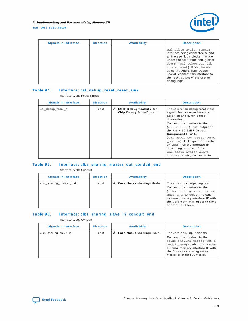
Signals in Interface Direction Availability Description
cal_debug_avalon_masterinterface being connected to andall the user logic blocks that areunder the calibration debug clockdomain (cal_debug_out_clkclock reset). If you are notusing the Altera EMIF DebugToolkit, connect this interface tothe reset output of the customdebug logic.
Table 94. Interface: cal_debug_reset_reset_sinkInterface type: Reset Intput
Signals in Interface Direction Availability Description
cal_debug_reset_n Input • EMIF Debug Toolkit / On-Chip Debug Port=Export
The calibration debug reset inputsignal. Require asynchronousassertion and synchronousdeassertion.Connect this interface to the(avl_rst_out) reset output ofthe Arria 10 EMIF DebugComponent IP or to(cal_debug_out_reset_reset_source) clock input of the otherexternal memory interface IP,depending on which IP thecal_debug_avalon_slaveinterface is being connected to.
Table 95. Interface: clks_sharing_master_out_conduit_endInterface type: Conduit
Signals in Interface Direction Availability Description
clks_sharing_master_out Input • Core clocks sharing=Master The core clock output signals.Connect this interface to the(clks_sharing_slave_in_conduit_end) conduit of the otherexternal memory interface IP withthe Core clock sharing set to slaveor other PLL Slave.
Table 96. Interface: clks_sharing_slave_in_conduit_endInterface type: Conduit
Signals in Interface Direction Availability Description
clks_sharing_slave_in Input • Core clocks sharing=Slave The core clock input signals.Connect this interface to the(clks_sharing_master_out_conduit_end) conduit of the otherexternal memory interface IP withthe Core clock sharing set toMaster or other PLL Master.
7. Implementing and Parameterizing Memory IP
EMI_DG | 2017.05.08
Send Feedback External Memory Interface Handbook Volume 2: Design Guidelines
253
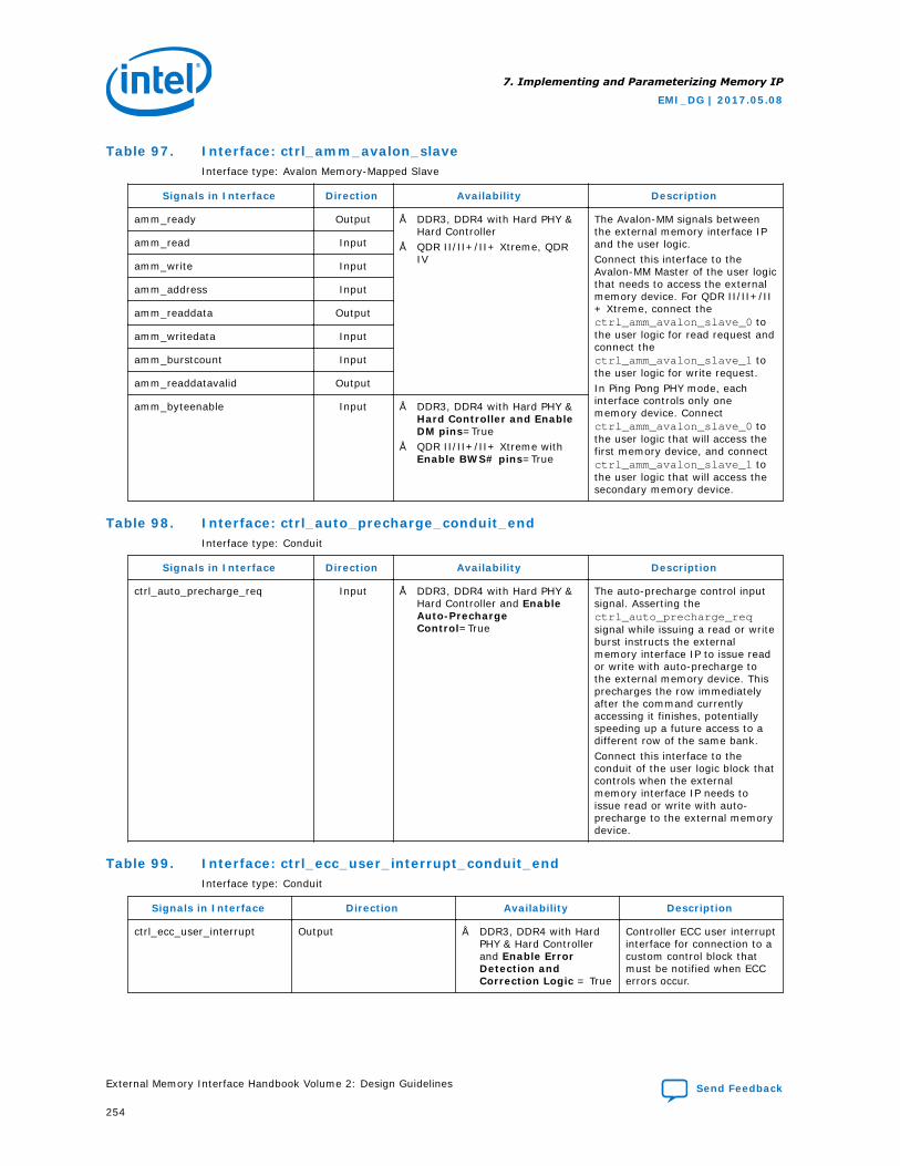
Table 97. Interface: ctrl_amm_avalon_slaveInterface type: Avalon Memory-Mapped Slave
Signals in Interface Direction Availability Description
amm_ready Output • DDR3, DDR4 with Hard PHY &Hard Controller
• QDR II/II+/II+ Xtreme, QDRIV
The Avalon-MM signals betweenthe external memory interface IPand the user logic.Connect this interface to theAvalon-MM Master of the user logicthat needs to access the externalmemory device. For QDR II/II+/II+ Xtreme, connect thectrl_amm_avalon_slave_0 tothe user logic for read request andconnect thectrl_amm_avalon_slave_1 tothe user logic for write request.In Ping Pong PHY mode, eachinterface controls only onememory device. Connectctrl_amm_avalon_slave_0 tothe user logic that will access thefirst memory device, and connectctrl_amm_avalon_slave_1 tothe user logic that will access thesecondary memory device.
amm_read Input
amm_write Input
amm_address Input
amm_readdata Output
amm_writedata Input
amm_burstcount Input
amm_readdatavalid Output
amm_byteenable Input • DDR3, DDR4 with Hard PHY &Hard Controller and EnableDM pins=True
• QDR II/II+/II+ Xtreme withEnable BWS# pins=True
Table 98. Interface: ctrl_auto_precharge_conduit_endInterface type: Conduit
Signals in Interface Direction Availability Description
ctrl_auto_precharge_req Input • DDR3, DDR4 with Hard PHY &Hard Controller and EnableAuto-PrechargeControl=True
The auto-precharge control inputsignal. Asserting thectrl_auto_precharge_reqsignal while issuing a read or writeburst instructs the externalmemory interface IP to issue reador write with auto-precharge tothe external memory device. Thisprecharges the row immediatelyafter the command currentlyaccessing it finishes, potentiallyspeeding up a future access to adifferent row of the same bank.Connect this interface to theconduit of the user logic block thatcontrols when the externalmemory interface IP needs toissue read or write with auto-precharge to the external memorydevice.
Table 99. Interface: ctrl_ecc_user_interrupt_conduit_endInterface type: Conduit
Signals in Interface Direction Availability Description
ctrl_ecc_user_interrupt Output • DDR3, DDR4 with HardPHY & Hard Controllerand Enable ErrorDetection andCorrection Logic = True
Controller ECC user interruptinterface for connection to acustom control block thatmust be notified when ECCerrors occur.
7. Implementing and Parameterizing Memory IP
EMI_DG | 2017.05.08
External Memory Interface Handbook Volume 2: Design Guidelines Send Feedback
254
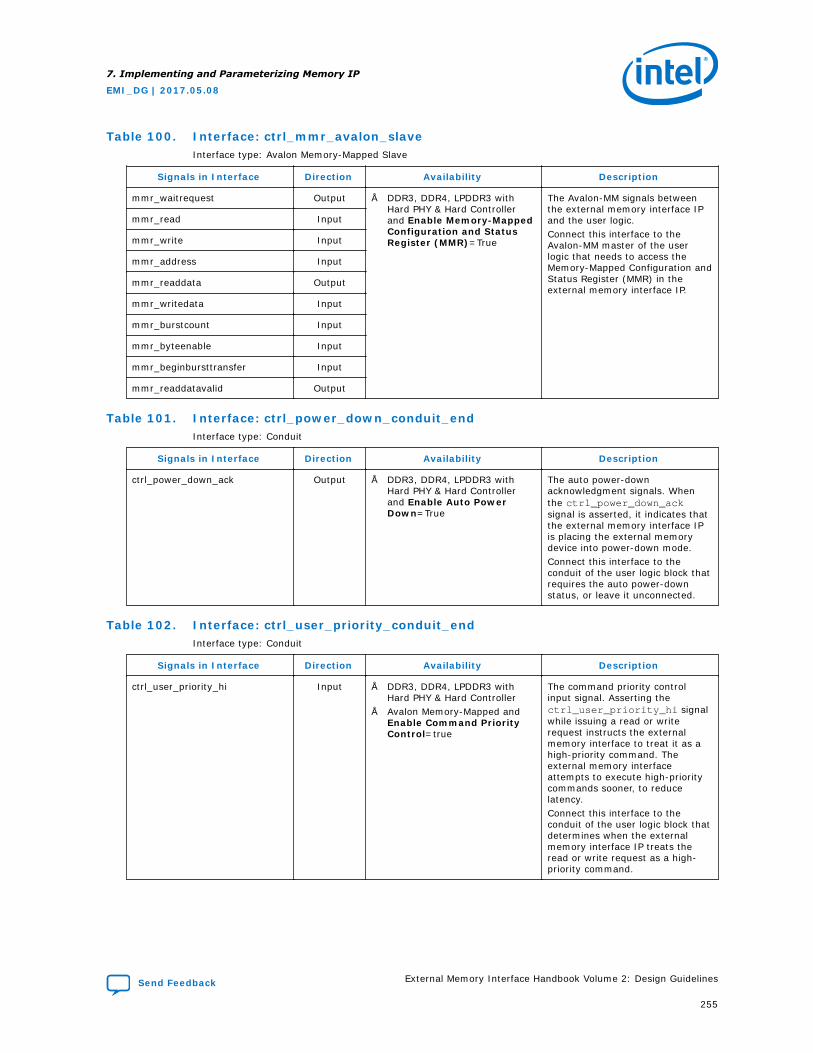
Table 100. Interface: ctrl_mmr_avalon_slaveInterface type: Avalon Memory-Mapped Slave
Signals in Interface Direction Availability Description
mmr_waitrequest Output • DDR3, DDR4, LPDDR3 withHard PHY & Hard Controllerand Enable Memory-MappedConfiguration and StatusRegister (MMR)=True
The Avalon-MM signals betweenthe external memory interface IPand the user logic.Connect this interface to theAvalon-MM master of the userlogic that needs to access theMemory-Mapped Configuration andStatus Register (MMR) in theexternal memory interface IP.
mmr_read Input
mmr_write Input
mmr_address Input
mmr_readdata Output
mmr_writedata Input
mmr_burstcount Input
mmr_byteenable Input
mmr_beginbursttransfer Input
mmr_readdatavalid Output
Table 101. Interface: ctrl_power_down_conduit_endInterface type: Conduit
Signals in Interface Direction Availability Description
ctrl_power_down_ack Output • DDR3, DDR4, LPDDR3 withHard PHY & Hard Controllerand Enable Auto PowerDown=True
The auto power-downacknowledgment signals. Whenthe ctrl_power_down_acksignal is asserted, it indicates thatthe external memory interface IPis placing the external memorydevice into power-down mode.Connect this interface to theconduit of the user logic block thatrequires the auto power-downstatus, or leave it unconnected.
Table 102. Interface: ctrl_user_priority_conduit_endInterface type: Conduit
Signals in Interface Direction Availability Description
ctrl_user_priority_hi Input • DDR3, DDR4, LPDDR3 withHard PHY & Hard Controller
• Avalon Memory-Mapped andEnable Command PriorityControl=true
The command priority controlinput signal. Asserting thectrl_user_priority_hi signalwhile issuing a read or writerequest instructs the externalmemory interface to treat it as ahigh-priority command. Theexternal memory interfaceattempts to execute high-prioritycommands sooner, to reducelatency.Connect this interface to theconduit of the user logic block thatdetermines when the externalmemory interface IP treats theread or write request as a high-priority command.
7. Implementing and Parameterizing Memory IP
EMI_DG | 2017.05.08
Send Feedback External Memory Interface Handbook Volume 2: Design Guidelines
255
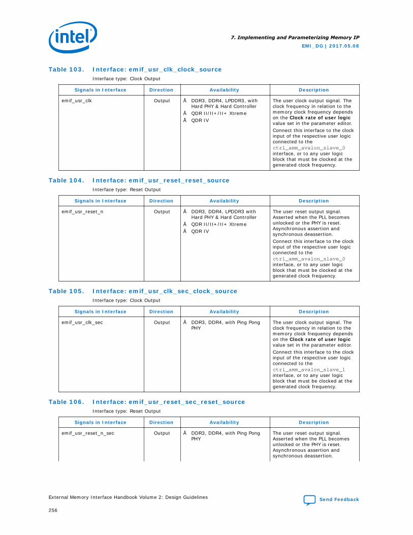
Table 103. Interface: emif_usr_clk_clock_sourceInterface type: Clock Output
Signals in Interface Direction Availability Description
emif_usr_clk Output • DDR3, DDR4, LPDDR3, withHard PHY & Hard Controller
• QDR II/II+/II+ Xtreme• QDR IV
The user clock output signal. Theclock frequency in relation to thememory clock frequency dependson the Clock rate of user logicvalue set in the parameter editor.Connect this interface to the clockinput of the respective user logicconnected to thectrl_amm_avalon_slave_0interface, or to any user logicblock that must be clocked at thegenerated clock frequency.
Table 104. Interface: emif_usr_reset_reset_sourceInterface type: Reset Output
Signals in Interface Direction Availability Description
emif_usr_reset_n Output • DDR3, DDR4, LPDDR3 withHard PHY & Hard Controller
• QDR II/II+/II+ Xtreme• QDR IV
The user reset output signal.Asserted when the PLL becomesunlocked or the PHY is reset.Asynchronous assertion andsynchronous deassertion.Connect this interface to the clockinput of the respective user logicconnected to thectrl_amm_avalon_slave_0interface, or to any user logicblock that must be clocked at thegenerated clock frequency.
Table 105. Interface: emif_usr_clk_sec_clock_sourceInterface type: Clock Output
Signals in Interface Direction Availability Description
emif_usr_clk_sec Output • DDR3, DDR4, with Ping PongPHY
The user clock output signal. Theclock frequency in relation to thememory clock frequency dependson the Clock rate of user logicvalue set in the parameter editor.Connect this interface to the clockinput of the respective user logicconnected to thectrl_amm_avalon_slave_1interface, or to any user logicblock that must be clocked at thegenerated clock frequency.
Table 106. Interface: emif_usr_reset_sec_reset_sourceInterface type: Reset Output
Signals in Interface Direction Availability Description
emif_usr_reset_n_sec Output • DDR3, DDR4, with Ping PongPHY
The user reset output signal.Asserted when the PLL becomesunlocked or the PHY is reset.Asynchronous assertion andsynchronous deassertion.
7. Implementing and Parameterizing Memory IP
EMI_DG | 2017.05.08
External Memory Interface Handbook Volume 2: Design Guidelines Send Feedback
256
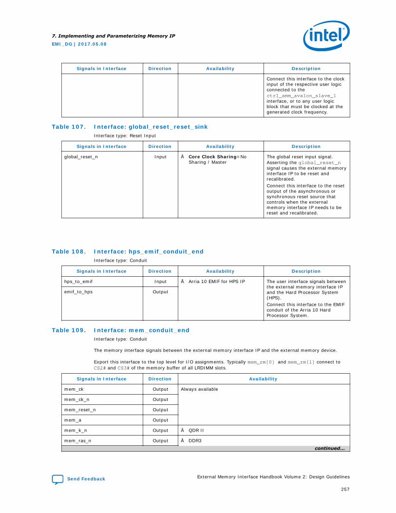
Signals in Interface Direction Availability Description
Connect this interface to the clockinput of the respective user logicconnected to thectrl_amm_avalon_slave_1interface, or to any user logicblock that must be clocked at thegenerated clock frequency.
Table 107. Interface: global_reset_reset_sinkInterface type: Reset Input
Signals in Interface Direction Availability Description
global_reset_n Input • Core Clock Sharing=NoSharing / Master
The global reset input signal.Asserting the global_reset_nsignal causes the external memoryinterface IP to be reset andrecalibrated.Connect this interface to the resetoutput of the asynchronous orsynchronous reset source thatcontrols when the externalmemory interface IP needs to bereset and recalibrated.
Table 108. Interface: hps_emif_conduit_endInterface type: Conduit
Signals in Interface Direction Availability Description
hps_to_emif Input • Arria 10 EMIF for HPS IP The user interface signals betweenthe external memory interface IPand the Hard Processor System(HPS).Connect this interface to the EMIFconduit of the Arria 10 HardProcessor System.
emif_to_hps Output
Table 109. Interface: mem_conduit_endInterface type: Conduit
The memory interface signals between the external memory interface IP and the external memory device.
Export this interface to the top level for I/O assignments. Typically mem_rm[0] and mem_rm[1] connect toCS2# and CS3# of the memory buffer of all LRDIMM slots.
Signals in Interface Direction Availability
mem_ck Output Always available
mem_ck_n Output
mem_reset_n Output
mem_a Output
mem_k_n Output • QDR II
mem_ras_n Output • DDR3
continued...
7. Implementing and Parameterizing Memory IP
EMI_DG | 2017.05.08
Send Feedback External Memory Interface Handbook Volume 2: Design Guidelines
257
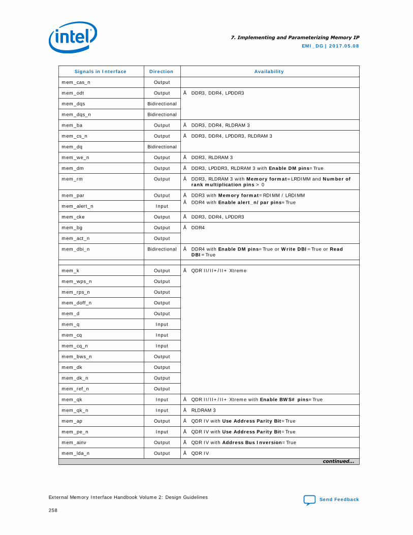
Signals in Interface Direction Availability
mem_cas_n Output
mem_odt Output • DDR3, DDR4, LPDDR3
mem_dqs Bidirectional
mem_dqs_n Bidirectional
mem_ba Output • DDR3, DDR4, RLDRAM 3
mem_cs_n Output • DDR3, DDR4, LPDDR3, RLDRAM 3
mem_dq Bidirectional
mem_we_n Output • DDR3, RLDRAM 3
mem_dm Output • DDR3, LPDDR3, RLDRAM 3 with Enable DM pins=True
mem_rm Output • DDR3, RLDRAM 3 with Memory format=LRDIMM and Number ofrank multiplication pins > 0
mem_par Output • DDR3 with Memory format=RDIMM / LRDIMM• DDR4 with Enable alert_n/par pins=True
mem_alert_n Input
mem_cke Output • DDR3, DDR4, LPDDR3
mem_bg Output • DDR4
mem_act_n Output
mem_dbi_n Bidirectional • DDR4 with Enable DM pins=True or Write DBI=True or ReadDBI=True
mem_k Output • QDR II/II+/II+ Xtreme
mem_wps_n Output
mem_rps_n Output
mem_doff_n Output
mem_d Output
mem_q Input
mem_cq Input
mem_cq_n Input
mem_bws_n Output
mem_dk Output
mem_dk_n Output
mem_ref_n Output
mem_qk Input • QDR II/II+/II+ Xtreme with Enable BWS# pins=True
mem_qk_n Input • RLDRAM 3
mem_ap Output • QDR IV with Use Address Parity Bit=True
mem_pe_n Input • QDR IV with Use Address Parity Bit=True
mem_ainv Output • QDR IV with Address Bus Inversion=True
mem_lda_n Output • QDR IV
continued...
7. Implementing and Parameterizing Memory IP
EMI_DG | 2017.05.08
External Memory Interface Handbook Volume 2: Design Guidelines Send Feedback
258
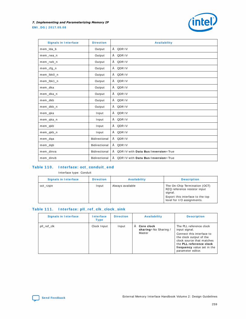
Signals in Interface Direction Availability
mem_lda_b Output • QDR IV
mem_rwa_n Output • QDR IV
mem_rwb_n Output • QDR IV
mem_cfg_n Output • QDR IV
mem_lbk0_n Output • QDR IV
mem_lbk1_n Output • QDR IV
mem_dka Output • QDR IV
mem_dka_n Output • QDR IV
mem_dkb Output • QDR IV
mem_dkb_n Output • QDR IV
mem_qka Input • QDR IV
mem_qka_n Input • QDR IV
mem_qkb Input • QDR IV
mem_qkb_n Input • QDR IV
mem_dqa Bidirectional • QDR IV
mem_dqb Bidirectional • QDR IV
mem_dinva Bidirectional • QDR IV with Data Bus Inversion=True
mem_dinvb Bidirectional • QDR IV with Data Bus Inversion=True
Table 110. Interface: oct_conduit_endInterface type: Conduit
Signals in Interface Direction Availability Description
oct_rzqin Input Always available The On-Chip Termination (OCT)RZQ reference resistor inputsignal.Export this interface to the toplevel for I/O assignments.
Table 111. Interface: pll_ref_clk_clock_sink
Signals in Interface InterfaceType
Direction Availability Description
pll_ref_clk Clock Input Input • Core clocksharing=No Sharing /Master
The PLL reference clockinput signal.Connect this interface tothe clock output of theclock source that matchesthe PLL reference clockfrequency value set in theparameter editor.
7. Implementing and Parameterizing Memory IP
EMI_DG | 2017.05.08
Send Feedback External Memory Interface Handbook Volume 2: Design Guidelines
259
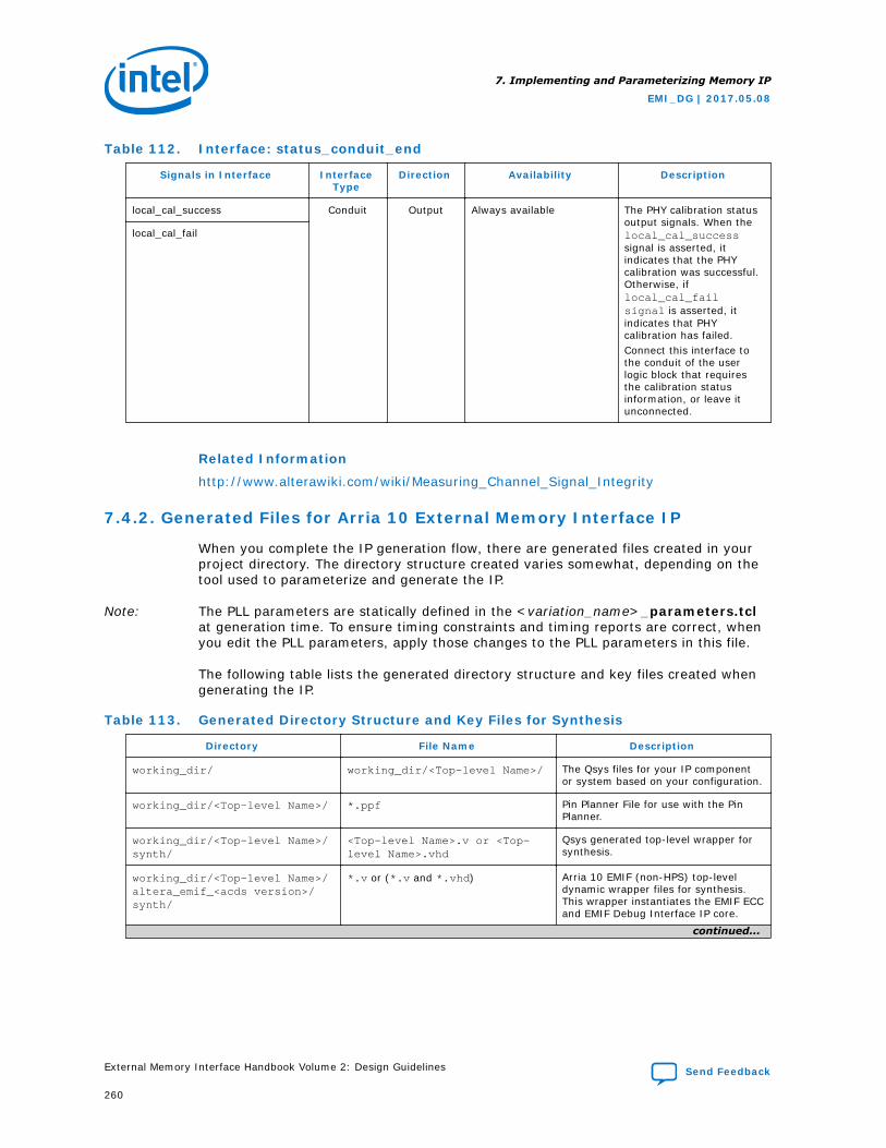
Table 112. Interface: status_conduit_end
Signals in Interface InterfaceType
Direction Availability Description
local_cal_success Conduit Output Always available The PHY calibration statusoutput signals. When thelocal_cal_successsignal is asserted, itindicates that the PHYcalibration was successful.Otherwise, iflocal_cal_failsignal is asserted, itindicates that PHYcalibration has failed.Connect this interface tothe conduit of the userlogic block that requiresthe calibration statusinformation, or leave itunconnected.
local_cal_fail
Related Information
http://www.alterawiki.com/wiki/Measuring_Channel_Signal_Integrity
7.4.2. Generated Files for Arria 10 External Memory Interface IP
When you complete the IP generation flow, there are generated files created in yourproject directory. The directory structure created varies somewhat, depending on thetool used to parameterize and generate the IP.
Note: The PLL parameters are statically defined in the <variation_name>_parameters.tclat generation time. To ensure timing constraints and timing reports are correct, whenyou edit the PLL parameters, apply those changes to the PLL parameters in this file.
The following table lists the generated directory structure and key files created whengenerating the IP.
Table 113. Generated Directory Structure and Key Files for Synthesis
Directory File Name Description
working_dir/ working_dir/<Top-level Name>/ The Qsys files for your IP componentor system based on your configuration.
working_dir/<Top-level Name>/ *.ppf Pin Planner File for use with the PinPlanner.
working_dir/<Top-level Name>/synth/
<Top-level Name>.v or <Top-level Name>.vhd
Qsys generated top-level wrapper forsynthesis.
working_dir/<Top-level Name>/altera_emif_<acds version>/synth/
*.v or (*.v and *.vhd) Arria 10 EMIF (non-HPS) top-leveldynamic wrapper files for synthesis.This wrapper instantiates the EMIF ECCand EMIF Debug Interface IP core.
continued...
7. Implementing and Parameterizing Memory IP
EMI_DG | 2017.05.08
External Memory Interface Handbook Volume 2: Design Guidelines Send Feedback
260
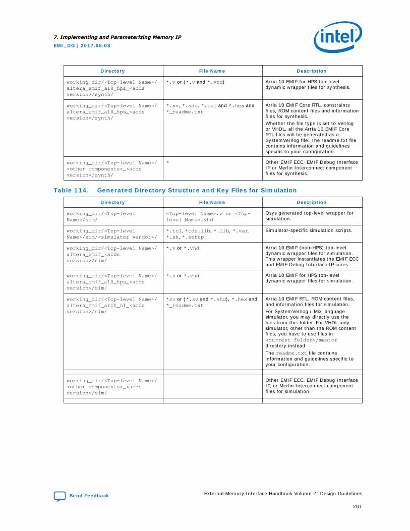
Directory File Name Description
working_dir/<Top-level Name>/altera_emif_a10_hps_<acdsversion>/synth/
*.v or (*.v and *.vhd) Arria 10 EMIF for HPS top-leveldynamic wrapper files for synthesis.
working_dir/<Top-level Name>/altera_emif_a10_hps_<acdsversion>/synth/
*.sv, *.sdc, *.tcl and *.hex and*_readme.txt
Arria 10 EMIF Core RTL, constraintsfiles, ROM content files and informationfiles for synthesis.Whether the file type is set to Verilogor VHDL, all the Arria 10 EMIF CoreRTL files will be generated as aSystemVerilog file. The readme.txt filecontains information and guidelinesspecific to your configuration.
working_dir/<Top-level Name>/<other components>_<acdsversion>/synth/
* Other EMIF ECC, EMIF Debug InterfaceIP or Merlin Interconnect componentfiles for synthesis.
Table 114. Generated Directory Structure and Key Files for Simulation
Directory File Name Description
working_dir/<Top-levelName>/sim/
<Top-level Name>.v or <Top-level Name>.vhd
Qsys generated top-level wrapper forsimulation.
working_dir/<Top-levelName>/sim/<simulator vendor>/
*.tcl, *cds.lib, *.lib, *.var,*.sh, *.setup
Simulator-specific simulation scripts.
working_dir/<Top-level Name>/altera_emif_<acdsversion>/sim/
*.v or *.vhd Arria 10 EMIF (non-HPS) top-leveldynamic wrapper files for simulation.This wrapper instantiates the EMIF ECCand EMIF Debug Interface IP cores.
working_dir/<Top-level Name>/altera_emif_a10_hps_<acdsversion>/sim/
*.v or *.vhd Arria 10 EMIF for HPS top-leveldynamic wrapper files for simulation.
working_dir/<Top-level Name>/altera_emif_arch_nf_<acdsversion>/sim/
*sv or (*.sv and *.vhd), *.hex and*_readme.txt
Arria 10 EMIF RTL, ROM content files,and information files for simulation.For SystemVerilog / Mix languagesimulator, you may directly use thefiles from this folder. For VHDL-onlysimulator, other than the ROM contentfiles, you have to use files in<current folder>/mentordirectory instead.The readme.txt file containsinformation and guidelines specific toyour configuration.
working_dir/<Top-level Name>/<other components>_<acdsversion>/sim/
Other EMIF ECC, EMIF Debug InterfaceIP, or Merlin Interconnect componentfiles for simulation
7. Implementing and Parameterizing Memory IP
EMI_DG | 2017.05.08
Send Feedback External Memory Interface Handbook Volume 2: Design Guidelines
261
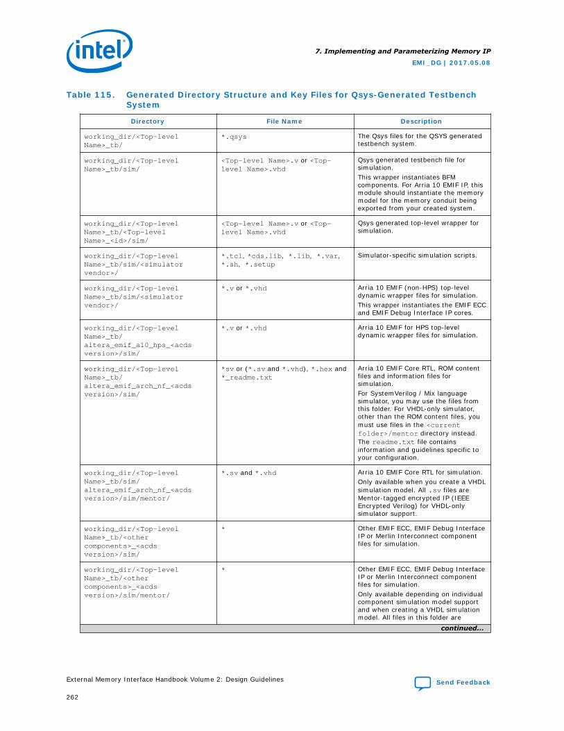
Table 115. Generated Directory Structure and Key Files for Qsys-Generated TestbenchSystem
Directory File Name Description
working_dir/<Top-levelName>_tb/
*.qsys The Qsys files for the QSYS generatedtestbench system.
working_dir/<Top-levelName>_tb/sim/
<Top-level Name>.v or <Top-level Name>.vhd
Qsys generated testbench file forsimulation.This wrapper instantiates BFMcomponents. For Arria 10 EMIF IP, thismodule should instantiate the memorymodel for the memory conduit beingexported from your created system.
working_dir/<Top-levelName>_tb/<Top-levelName>_<id>/sim/
<Top-level Name>.v or <Top-level Name>.vhd
Qsys generated top-level wrapper forsimulation.
working_dir/<Top-levelName>_tb/sim/<simulatorvendor>/
*.tcl, *cds.lib, *.lib, *.var,*.sh, *.setup
Simulator-specific simulation scripts.
working_dir/<Top-levelName>_tb/sim/<simulatorvendor>/
*.v or *.vhd Arria 10 EMIF (non-HPS) top-leveldynamic wrapper files for simulation.This wrapper instantiates the EMIF ECCand EMIF Debug Interface IP cores.
working_dir/<Top-levelName>_tb/altera_emif_a10_hps_<acdsversion>/sim/
*.v or *.vhd Arria 10 EMIF for HPS top-leveldynamic wrapper files for simulation.
working_dir/<Top-levelName>_tb/altera_emif_arch_nf_<acdsversion>/sim/
*sv or (*.sv and *.vhd), *.hex and*_readme.txt
Arria 10 EMIF Core RTL, ROM contentfiles and information files forsimulation.For SystemVerilog / Mix languagesimulator, you may use the files fromthis folder. For VHDL-only simulator,other than the ROM content files, youmust use files in the <currentfolder>/mentor directory instead.The readme.txt file containsinformation and guidelines specific toyour configuration.
working_dir/<Top-levelName>_tb/sim/altera_emif_arch_nf_<acdsversion>/sim/mentor/
*.sv and *.vhd Arria 10 EMIF Core RTL for simulation.Only available when you create a VHDLsimulation model. All .sv files areMentor-tagged encrypted IP (IEEEEncrypted Verilog) for VHDL-onlysimulator support.
working_dir/<Top-levelName>_tb/<othercomponents>_<acdsversion>/sim/
* Other EMIF ECC, EMIF Debug InterfaceIP or Merlin Interconnect componentfiles for simulation.
working_dir/<Top-levelName>_tb/<othercomponents>_<acdsversion>/sim/mentor/
* Other EMIF ECC, EMIF Debug InterfaceIP or Merlin Interconnect componentfiles for simulation.Only available depending on individualcomponent simulation model supportand when creating a VHDL simulationmodel. All files in this folder are
continued...
7. Implementing and Parameterizing Memory IP
EMI_DG | 2017.05.08
External Memory Interface Handbook Volume 2: Design Guidelines Send Feedback
262
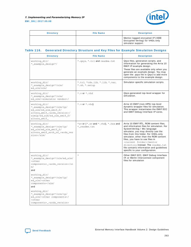
Directory File Name Description
Mentor-tagged encrypted IP (IEEEEncrypted Verilog) for VHDL-onlysimulator support.
Table 116. Generated Directory Structure and Key Files for Example Simulation Designs
Directory File Name Description
working_dir/*_example_design*/
*.qsys, *.tcl and readme.txt Qsys files, generation scripts, andinformation for generating the Arria 10EMIF IP example design.These files are available only when yougenerate an example design. You mayopen the .qsys file in Qsys to add morecomponents to the example design.
working_dir/*_example_design*/sim/ed_sim/sim/
*.tcl, *cds.lib, *.lib, *.var,*.sh, *.setup
Simulator-specific simulation scripts.
working_dir/*_example_design*/sim/ed_sim/<simulator vendor>/
*.v or *.vhd Qsys-generated top-level wrapper forsimulation.
working_dir/*_example_design*/sim/ip/ed_sim/ed_sim_emif_0/altera_emif_<acds_version>/simip/ed_sim/ed_sim_emif_0/altera_emif_
*.v or *.vhd) Arria 10 EMIF (non-HPS) top-leveldynamic wrapper files for simulation.This wrapper instantiates the EMIF ECCand EMIF Debug Interface IP cores.
working_dir/*_example_design*/sim/ip/ed_sim/ed_sim_emif_0/altera_emif_arch_nf_<acds_version>/sim/
*sv or (*.sv and *.vhd), *.hex and*_readme.txt
Arria 10 EMIF RTL, ROM content files,and information files for simulation. ForSystemVerilog / Mix languagesimulator, you may directly use thefiles from this folder. For VHDL-onlysimulator, other than the ROM contentfiles, you have to use files in<current folder>/mentordirectory instead. The readme.txtfile contains information and guidelinesspecific to your configuration.
working_dir/*_example_design*/sim/ed_sim/<othercomponents>_<acds_version>/sim/
and
working_dir/*_example_design*/sim/ip/ed_sim/<othercomponents>/sim/
and
working_dir/*_example_design*/sim/ip/ed_sim/<other components>/<othercomponents>_<acds_version>
* Other EMIF ECC, EMIF Debug InterfaceIP, or Merlin Interconnect componentfiles for simulation
7. Implementing and Parameterizing Memory IP
EMI_DG | 2017.05.08
Send Feedback External Memory Interface Handbook Volume 2: Design Guidelines
263
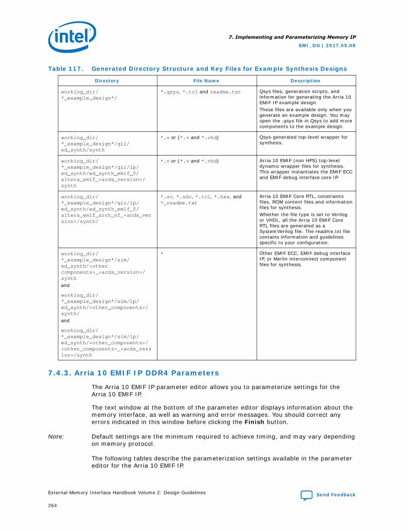
Table 117. Generated Directory Structure and Key Files for Example Synthesis Designs
Directory File Name Description
working_dir/*_example_design*/
*.qsys, *.tcl and readme.txt Qsys files, generation scripts, andinformation for generating the Arria 10EMIF IP example design.These files are available only when yougenerate an example design. You mayopen the .qsys file in Qsys to add morecomponents to the example design.
working_dir/*_example_design*/qii/ed_synth/synth
*.v or (*.v and *.vhd) Qsys-generated top-level wrapper forsynthesis.
working_dir/*_example_design*/qii/ip/ed_synth/ed_synth_emif_0/altera_emif_<acds_version>/synth
*.v or (*.v and *.vhd) Arria 10 EMIF (non HPS) top-leveldynamic wrapper files for synthesis.This wrapper instantiates the EMIF ECCand EMIF debug interface core IP.
working_dir/*_example_design*/qii/ip/ed_synth/ed_synth_emif_0/altera_emif_arch_nf_<acds_version>/synth/
*.sv, *.sdc, *.tcl, *.hex, and*_readme.txt
Arria 10 EMIF Core RTL, constraintsfiles, ROM content files and informationfiles for synthesis.Whether the file type is set to Verilogor VHDL, all the Arria 10 EMIF CoreRTL files are generated as aSystemVerilog file. The readme.txt filecontains information and guidelinesspecific to your configuration.
working_dir/*_example_design*/sim/ed_synth/<othercomponents>_<acds_version>/synth
and
working_dir/*_example_design*/sim/ip/ed_synth/<other_components>/synth/
and
working_dir/*_example_design*/sim/ip/ed_synth/<other_components>/<other_components>_<acds_version>/synth
* Other EMIF ECC, EMIF debug interfaceIP, or Merlin interconnect componentfiles for synthesis.
7.4.3. Arria 10 EMIF IP DDR4 Parameters
The Arria 10 EMIF IP parameter editor allows you to parameterize settings for theArria 10 EMIF IP.
The text window at the bottom of the parameter editor displays information about thememory interface, as well as warning and error messages. You should correct anyerrors indicated in this window before clicking the Finish button.
Note: Default settings are the minimum required to achieve timing, and may vary dependingon memory protocol.
The following tables describe the parameterization settings available in the parametereditor for the Arria 10 EMIF IP.
7. Implementing and Parameterizing Memory IP
EMI_DG | 2017.05.08
External Memory Interface Handbook Volume 2: Design Guidelines Send Feedback
264
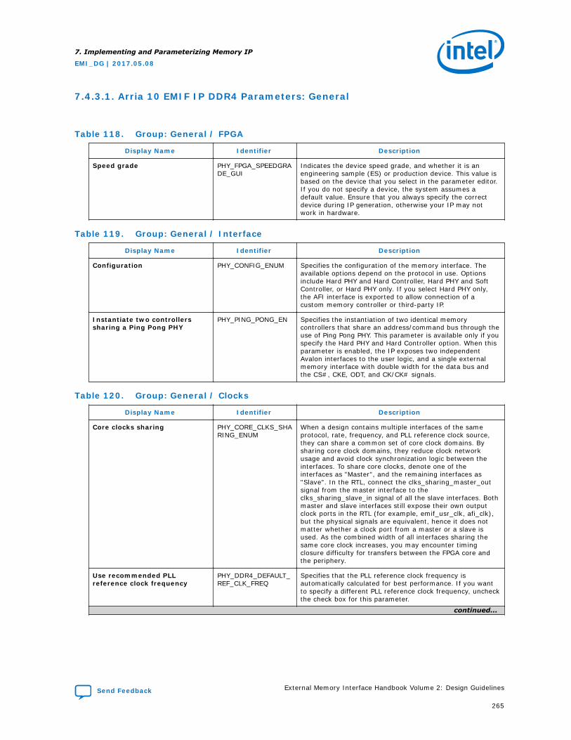
7.4.3.1. Arria 10 EMIF IP DDR4 Parameters: General
Table 118. Group: General / FPGA
Display Name Identifier Description
Speed grade PHY_FPGA_SPEEDGRADE_GUI
Indicates the device speed grade, and whether it is anengineering sample (ES) or production device. This value isbased on the device that you select in the parameter editor.If you do not specify a device, the system assumes adefault value. Ensure that you always specify the correctdevice during IP generation, otherwise your IP may notwork in hardware.
Table 119. Group: General / Interface
Display Name Identifier Description
Configuration PHY_CONFIG_ENUM Specifies the configuration of the memory interface. Theavailable options depend on the protocol in use. Optionsinclude Hard PHY and Hard Controller, Hard PHY and SoftController, or Hard PHY only. If you select Hard PHY only,the AFI interface is exported to allow connection of acustom memory controller or third-party IP.
Instantiate two controllerssharing a Ping Pong PHY
PHY_PING_PONG_EN Specifies the instantiation of two identical memorycontrollers that share an address/command bus through theuse of Ping Pong PHY. This parameter is available only if youspecify the Hard PHY and Hard Controller option. When thisparameter is enabled, the IP exposes two independentAvalon interfaces to the user logic, and a single externalmemory interface with double width for the data bus andthe CS#, CKE, ODT, and CK/CK# signals.
Table 120. Group: General / Clocks
Display Name Identifier Description
Core clocks sharing PHY_CORE_CLKS_SHARING_ENUM
When a design contains multiple interfaces of the sameprotocol, rate, frequency, and PLL reference clock source,they can share a common set of core clock domains. Bysharing core clock domains, they reduce clock networkusage and avoid clock synchronization logic between theinterfaces. To share core clocks, denote one of theinterfaces as "Master", and the remaining interfaces as"Slave". In the RTL, connect the clks_sharing_master_outsignal from the master interface to theclks_sharing_slave_in signal of all the slave interfaces. Bothmaster and slave interfaces still expose their own outputclock ports in the RTL (for example, emif_usr_clk, afi_clk),but the physical signals are equivalent, hence it does notmatter whether a clock port from a master or a slave isused. As the combined width of all interfaces sharing thesame core clock increases, you may encounter timingclosure difficulty for transfers between the FPGA core andthe periphery.
Use recommended PLLreference clock frequency
PHY_DDR4_DEFAULT_REF_CLK_FREQ
Specifies that the PLL reference clock frequency isautomatically calculated for best performance. If you wantto specify a different PLL reference clock frequency, uncheckthe check box for this parameter.
continued...
7. Implementing and Parameterizing Memory IP
EMI_DG | 2017.05.08
Send Feedback External Memory Interface Handbook Volume 2: Design Guidelines
265
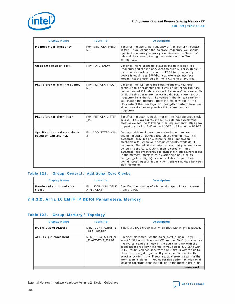
Display Name Identifier Description
Memory clock frequency PHY_MEM_CLK_FREQ_MHZ
Specifies the operating frequency of the memory interfacein MHz. If you change the memory frequency, you shouldupdate the memory latency parameters on the "Memory"tab and the memory timing parameters on the "MemTiming" tab.
Clock rate of user logic PHY_RATE_ENUM Specifies the relationship between the user logic clockfrequency and the memory clock frequency. For example, ifthe memory clock sent from the FPGA to the memorydevice is toggling at 800MHz, a quarter-rate interfacemeans that the user logic in the FPGA runs at 200MHz.
PLL reference clock frequency PHY_REF_CLK_FREQ_MHZ
Specifies the PLL reference clock frequency. You mustconfigure this parameter only if you do not check the "Userecommended PLL reference clock frequency" parameter. Toconfigure this parameter, select a valid PLL reference clockfrequency from the list. The values in the list can change ifyou change the memory interface frequency and/or theclock rate of the user logic. For best jitter performance, youshould use the fastest possible PLL reference clockfrequency.
PLL reference clock jitter PHY_REF_CLK_JITTER_PS
Specifies the peak-to-peak jitter on the PLL reference clocksource. The clock source of the PLL reference clock mustmeet or exceed the following jitter requirements: 10ps peakto peak, or 1.42ps RMS at 1e-12 BER, 1.22ps at 1e-16 BER.
Specify additional core clocksbased on existing PLL
PLL_ADD_EXTRA_CLKS
Displays additional parameters allowing you to createadditional output clocks based on the existing PLL. Thisparameter provides an alternative clock-generationmechanism for when your design exhausts available PLLresources. The additional output clocks that you create canbe fed into the core. Clock signals created with thisparameter are synchronous to each other, but asynchronousto the memory interface core clock domains (such asemif_usr_clk or afi_clk). You must follow proper clock-domain-crossing techniques when transferring data betweenclock domains.
Table 121. Group: General / Additional Core Clocks
Display Name Identifier Description
Number of additional coreclocks
PLL_USER_NUM_OF_EXTRA_CLKS
Specifies the number of additional output clocks to createfrom the PLL.
7.4.3.2. Arria 10 EMIF IP DDR4 Parameters: Memory
Table 122. Group: Memory / Topology
Display Name Identifier Description
DQS group of ALERT# MEM_DDR4_ALERT_N_DQS_GROUP
Select the DQS group with which the ALERT# pin is placed.
ALERT# pin placement MEM_DDR4_ALERT_N_PLACEMENT_ENUM
Specifies placement for the mem_alert_n signal. If youselect "I/O Lane with Address/Command Pins", you can pickthe I/O lane and pin index in the add/cmd bank with thesubsequent drop down menus. If you select "I/O Lane withDQS Group", you can specify the DQS group with which toplace the mem_alert_n pin. If you select "Automaticallyselect a location", the IP automatically selects a pin for themem_alert_n signal. If you select this option, no additionallocation constraints can be applied to the mem_alert_n pin,
continued...
7. Implementing and Parameterizing Memory IP
EMI_DG | 2017.05.08
External Memory Interface Handbook Volume 2: Design Guidelines Send Feedback
266
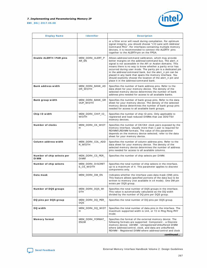
Display Name Identifier Description
or a fitter error will result during compilation. For optimumsignal integrity, you should choose "I/O Lane with Address/Command Pins". For interfaces containing multiple memorydevices, it is recommended to connect the ALERT# pinstogether to the ALERT#pin on the FPGA.
Enable ALERT#/PAR pins MEM_DDR4_ALERT_PAR_EN
Allows address/command calibration, which may providebetter margins on the address/command bus. The alert_nsignal is not accessible in the AFI or Avalon domains. Thismeans there is no way to know whether a parity error hasoccurred during user mode. The parity pin is a dedicated pinin the address/command bank, but the alert_n pin can beplaced in any bank that spans the memory interface. Youshould explicitly choose the location of the alert_n pin andplace it in the address/command bank.
Bank address width MEM_DDR4_BANK_ADDR_WIDTH
Specifies the number of bank address pins. Refer to thedata sheet for your memory device. The density of theselected memory device determines the number of bankaddress pins needed for access to all available banks.
Bank group width MEM_DDR4_BANK_GROUP_WIDTH
Specifies the number of bank group pins. Refer to the datasheet for your memory device. The density of the selectedmemory device determines the number of bank group pinsneeded for access to all available bank groups.
Chip ID width MEM_DDR4_CHIP_ID_WIDTH
Specifies the number of chip ID pins. Only applicable toregistered and load-reduced DIMMs that use 3DS/TSVmemory devices.
Number of clocks MEM_DDR4_CK_WIDTH
Specifies the number of CK/CK# clock pairs exposed by thememory interface. Usually more than 1 pair is required forRDIMM/LRDIMM formats. The value of this parameterdepends on the memory device selected; refer to the datasheet for your memory device.
Column address width MEM_DDR4_COL_ADDR_WIDTH
Specifies the number of column address pins. Refer to thedata sheet for your memory device. The density of theselected memory device determines the number of addresspins needed for access to all available columns.
Number of chip selects perDIMM
MEM_DDR4_CS_PER_DIMM
Specifies the number of chip selects per DIMM.
Number of chip selects MEM_DDR4_DISCRETE_CS_WIDTH
Specifies the total number of chip selects in the interface,up to a maximum of 4. This parameter applies to discretecomponents only.
Data mask MEM_DDR4_DM_EN Indicates whether the interface uses data mask (DM) pins.This feature allows specified portions of the data bus to bewritten to memory (not available in x4 mode). One DM pinexists per DQS group.
Number of DQS groups MEM_DDR4_DQS_WIDTH
Specifies the total number of DQS groups in the interface.This value is automatically calculated as the DQ widthdivided by the number of DQ pins per DQS group.
DQ pins per DQS group MEM_DDR4_DQ_PER_DQS
Specifies the total number of DQ pins per DQS group.
DQ width MEM_DDR4_DQ_WIDTH
Specifies the total number of data pins in the interface. Themaximum supported width is 144, or 72 in Ping Pong PHYmode.
Memory format MEM_DDR4_FORMAT_ENUM
Specifies the format of the external memory device. Thefollowing formats are supported: Component - a Discretememory device; UDIMM - Unregistered/Unbuffered DIMMwhere address/control, clock, and data are unbuffered;RDIMM - Registered DIMM where address/control and clock
continued...
7. Implementing and Parameterizing Memory IP
EMI_DG | 2017.05.08
Send Feedback External Memory Interface Handbook Volume 2: Design Guidelines
267
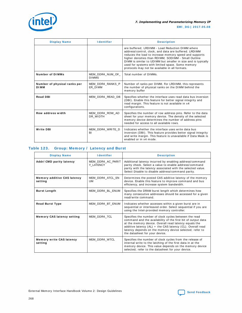
Display Name Identifier Description
are buffered; LRDIMM - Load Reduction DIMM whereaddress/control, clock, and data are buffered. LRDIMMreduces the load to increase memory speed and supportshigher densities than RDIMM; SODIMM - Small OutlineDIMM is similar to UDIMM but smaller in size and is typicallyused for systems with limited space. Some memoryprotocols may not be available in all formats.
Number of DIMMs MEM_DDR4_NUM_OF_DIMMS
Total number of DIMMs.
Number of physical ranks perDIMM
MEM_DDR4_RANKS_PER_DIMM
Number of ranks per DIMM. For LRDIMM, this representsthe number of physical ranks on the DIMM behind thememory buffer
Read DBI MEM_DDR4_READ_DBI
Specifies whether the interface uses read data bus inversion(DBI). Enable this feature for better signal integrity andread margin. This feature is not available in x4configurations.
Row address width MEM_DDR4_ROW_ADDR_WIDTH
Specifies the number of row address pins. Refer to the datasheet for your memory device. The density of the selectedmemory device determines the number of address pinsneeded for access to all available rows.
Write DBI MEM_DDR4_WRITE_DBI
Indicates whether the interface uses write data businversion (DBI). This feature provides better signal integrityand write margin. This feature is unavailable if Data Mask isenabled or in x4 mode.
Table 123. Group: Memory / Latency and Burst
Display Name Identifier Description
Addr/CMD parity latency MEM_DDR4_AC_PARITY_LATENCY
Additional latency incurred by enabling address/commandparity check. Select a value to enable address/commandparity with the latency associated with the selected value.Select Disable to disable address/command parity.
Memory additive CAS latencysetting
MEM_DDR4_ATCL_ENUM
Determines the posted CAS additive latency of the memorydevice. Enable this feature to improve command and busefficiency, and increase system bandwidth.
Burst Length MEM_DDR4_BL_ENUM Specifies the DRAM burst length which determines howmany consecutive addresses should be accessed for a givenread/write command.
Read Burst Type MEM_DDR4_BT_ENUM Indicates whether accesses within a given burst are insequential or interleaved order. Select sequential if you areusing the Intel-provided memory controller.
Memory CAS latency setting MEM_DDR4_TCL Specifies the number of clock cycles between the readcommand and the availability of the first bit of output dataat the memory device. Overall read latency equals theadditive latency (AL) + the CAS latency (CL). Overall readlatency depends on the memory device selected; refer tothe datasheet for your device.
Memory write CAS latencysetting
MEM_DDR4_WTCL Specifies the number of clock cycles from the release ofinternal write to the latching of the first data in at thememory device. This value depends on the memory deviceselected; refer to the datasheet for your device.
7. Implementing and Parameterizing Memory IP
EMI_DG | 2017.05.08
External Memory Interface Handbook Volume 2: Design Guidelines Send Feedback
268
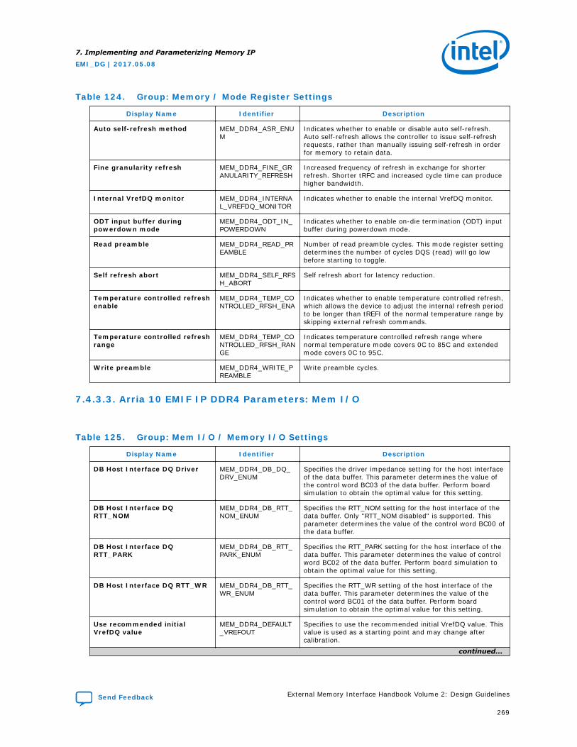
Table 124. Group: Memory / Mode Register Settings
Display Name Identifier Description
Auto self-refresh method MEM_DDR4_ASR_ENUM
Indicates whether to enable or disable auto self-refresh.Auto self-refresh allows the controller to issue self-refreshrequests, rather than manually issuing self-refresh in orderfor memory to retain data.
Fine granularity refresh MEM_DDR4_FINE_GRANULARITY_REFRESH
Increased frequency of refresh in exchange for shorterrefresh. Shorter tRFC and increased cycle time can producehigher bandwidth.
Internal VrefDQ monitor MEM_DDR4_INTERNAL_VREFDQ_MONITOR
Indicates whether to enable the internal VrefDQ monitor.
ODT input buffer duringpowerdown mode
MEM_DDR4_ODT_IN_POWERDOWN
Indicates whether to enable on-die termination (ODT) inputbuffer during powerdown mode.
Read preamble MEM_DDR4_READ_PREAMBLE
Number of read preamble cycles. This mode register settingdetermines the number of cycles DQS (read) will go lowbefore starting to toggle.
Self refresh abort MEM_DDR4_SELF_RFSH_ABORT
Self refresh abort for latency reduction.
Temperature controlled refreshenable
MEM_DDR4_TEMP_CONTROLLED_RFSH_ENA
Indicates whether to enable temperature controlled refresh,which allows the device to adjust the internal refresh periodto be longer than tREFI of the normal temperature range byskipping external refresh commands.
Temperature controlled refreshrange
MEM_DDR4_TEMP_CONTROLLED_RFSH_RANGE
Indicates temperature controlled refresh range wherenormal temperature mode covers 0C to 85C and extendedmode covers 0C to 95C.
Write preamble MEM_DDR4_WRITE_PREAMBLE
Write preamble cycles.
7.4.3.3. Arria 10 EMIF IP DDR4 Parameters: Mem I/O
Table 125. Group: Mem I/O / Memory I/O Settings
Display Name Identifier Description
DB Host Interface DQ Driver MEM_DDR4_DB_DQ_DRV_ENUM
Specifies the driver impedance setting for the host interfaceof the data buffer. This parameter determines the value ofthe control word BC03 of the data buffer. Perform boardsimulation to obtain the optimal value for this setting.
DB Host Interface DQRTT_NOM
MEM_DDR4_DB_RTT_NOM_ENUM
Specifies the RTT_NOM setting for the host interface of thedata buffer. Only "RTT_NOM disabled" is supported. Thisparameter determines the value of the control word BC00 ofthe data buffer.
DB Host Interface DQRTT_PARK
MEM_DDR4_DB_RTT_PARK_ENUM
Specifies the RTT_PARK setting for the host interface of thedata buffer. This parameter determines the value of controlword BC02 of the data buffer. Perform board simulation toobtain the optimal value for this setting.
DB Host Interface DQ RTT_WR MEM_DDR4_DB_RTT_WR_ENUM
Specifies the RTT_WR setting of the host interface of thedata buffer. This parameter determines the value of thecontrol word BC01 of the data buffer. Perform boardsimulation to obtain the optimal value for this setting.
Use recommended initialVrefDQ value
MEM_DDR4_DEFAULT_VREFOUT
Specifies to use the recommended initial VrefDQ value. Thisvalue is used as a starting point and may change aftercalibration.
continued...
7. Implementing and Parameterizing Memory IP
EMI_DG | 2017.05.08
Send Feedback External Memory Interface Handbook Volume 2: Design Guidelines
269
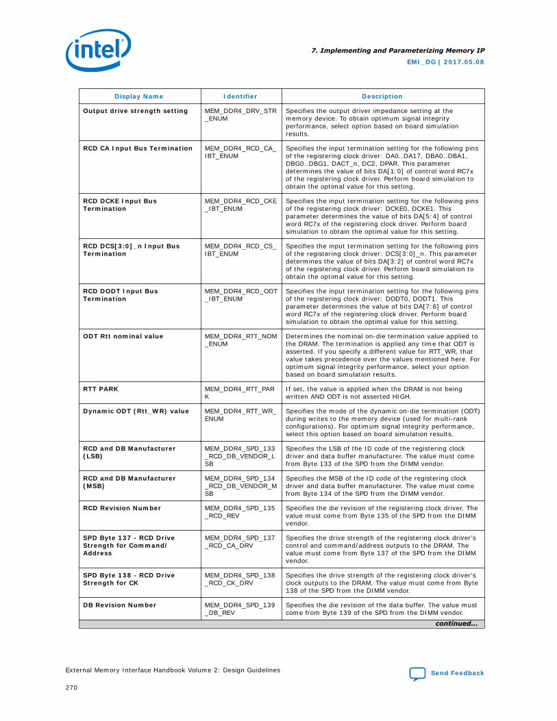
Display Name Identifier Description
Output drive strength setting MEM_DDR4_DRV_STR_ENUM
Specifies the output driver impedance setting at thememory device. To obtain optimum signal integrityperformance, select option based on board simulationresults.
RCD CA Input Bus Termination MEM_DDR4_RCD_CA_IBT_ENUM
Specifies the input termination setting for the following pinsof the registering clock driver: DA0..DA17, DBA0..DBA1,DBG0..DBG1, DACT_n, DC2, DPAR. This parameterdetermines the value of bits DA[1:0] of control word RC7xof the registering clock driver. Perform board simulation toobtain the optimal value for this setting.
RCD DCKE Input BusTermination
MEM_DDR4_RCD_CKE_IBT_ENUM
Specifies the input termination setting for the following pinsof the registering clock driver: DCKE0, DCKE1. Thisparameter determines the value of bits DA[5:4] of controlword RC7x of the registering clock driver. Perform boardsimulation to obtain the optimal value for this setting.
RCD DCS[3:0]_n Input BusTermination
MEM_DDR4_RCD_CS_IBT_ENUM
Specifies the input termination setting for the following pinsof the registering clock driver: DCS[3:0]_n. This parameterdetermines the value of bits DA[3:2] of control word RC7xof the registering clock driver. Perform board simulation toobtain the optimal value for this setting.
RCD DODT Input BusTermination
MEM_DDR4_RCD_ODT_IBT_ENUM
Specifies the input termination setting for the following pinsof the registering clock driver: DODT0, DODT1. Thisparameter determines the value of bits DA[7:6] of controlword RC7x of the registering clock driver. Perform boardsimulation to obtain the optimal value for this setting.
ODT Rtt nominal value MEM_DDR4_RTT_NOM_ENUM
Determines the nominal on-die termination value applied tothe DRAM. The termination is applied any time that ODT isasserted. If you specify a different value for RTT_WR, thatvalue takes precedence over the values mentioned here. Foroptimum signal integrity performance, select your optionbased on board simulation results.
RTT PARK MEM_DDR4_RTT_PARK
If set, the value is applied when the DRAM is not beingwritten AND ODT is not asserted HIGH.
Dynamic ODT (Rtt_WR) value MEM_DDR4_RTT_WR_ENUM
Specifies the mode of the dynamic on-die termination (ODT)during writes to the memory device (used for multi-rankconfigurations). For optimum signal integrity performance,select this option based on board simulation results.
RCD and DB Manufacturer(LSB)
MEM_DDR4_SPD_133_RCD_DB_VENDOR_LSB
Specifies the LSB of the ID code of the registering clockdriver and data buffer manufacturer. The value must comefrom Byte 133 of the SPD from the DIMM vendor.
RCD and DB Manufacturer(MSB)
MEM_DDR4_SPD_134_RCD_DB_VENDOR_MSB
Specifies the MSB of the ID code of the registering clockdriver and data buffer manufacturer. The value must comefrom Byte 134 of the SPD from the DIMM vendor.
RCD Revision Number MEM_DDR4_SPD_135_RCD_REV
Specifies the die revision of the registering clock driver. Thevalue must come from Byte 135 of the SPD from the DIMMvendor.
SPD Byte 137 - RCD DriveStrength for Command/Address
MEM_DDR4_SPD_137_RCD_CA_DRV
Specifies the drive strength of the registering clock driver'scontrol and command/address outputs to the DRAM. Thevalue must come from Byte 137 of the SPD from the DIMMvendor.
SPD Byte 138 - RCD DriveStrength for CK
MEM_DDR4_SPD_138_RCD_CK_DRV
Specifies the drive strength of the registering clock driver'sclock outputs to the DRAM. The value must come from Byte138 of the SPD from the DIMM vendor.
DB Revision Number MEM_DDR4_SPD_139_DB_REV
Specifies the die revision of the data buffer. The value mustcome from Byte 139 of the SPD from the DIMM vendor.
continued...
7. Implementing and Parameterizing Memory IP
EMI_DG | 2017.05.08
External Memory Interface Handbook Volume 2: Design Guidelines Send Feedback
270
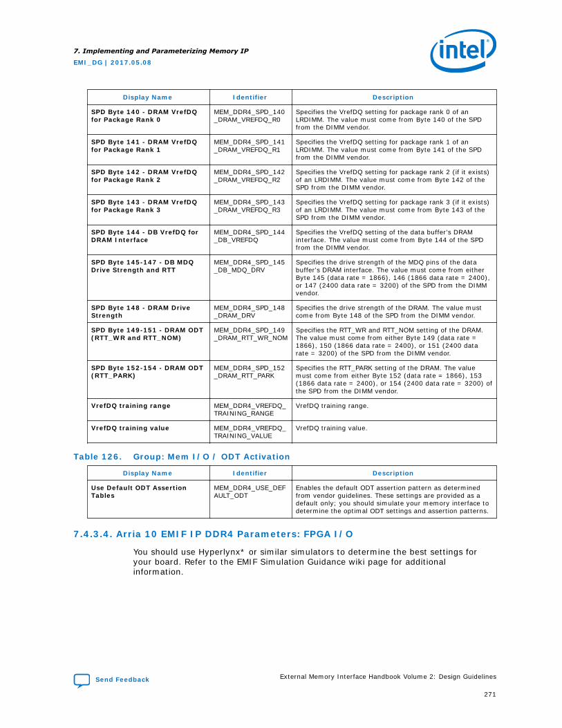
Display Name Identifier Description
SPD Byte 140 - DRAM VrefDQfor Package Rank 0
MEM_DDR4_SPD_140_DRAM_VREFDQ_R0
Specifies the VrefDQ setting for package rank 0 of anLRDIMM. The value must come from Byte 140 of the SPDfrom the DIMM vendor.
SPD Byte 141 - DRAM VrefDQfor Package Rank 1
MEM_DDR4_SPD_141_DRAM_VREFDQ_R1
Specifies the VrefDQ setting for package rank 1 of anLRDIMM. The value must come from Byte 141 of the SPDfrom the DIMM vendor.
SPD Byte 142 - DRAM VrefDQfor Package Rank 2
MEM_DDR4_SPD_142_DRAM_VREFDQ_R2
Specifies the VrefDQ setting for package rank 2 (if it exists)of an LRDIMM. The value must come from Byte 142 of theSPD from the DIMM vendor.
SPD Byte 143 - DRAM VrefDQfor Package Rank 3
MEM_DDR4_SPD_143_DRAM_VREFDQ_R3
Specifies the VrefDQ setting for package rank 3 (if it exists)of an LRDIMM. The value must come from Byte 143 of theSPD from the DIMM vendor.
SPD Byte 144 - DB VrefDQ forDRAM Interface
MEM_DDR4_SPD_144_DB_VREFDQ
Specifies the VrefDQ setting of the data buffer's DRAMinterface. The value must come from Byte 144 of the SPDfrom the DIMM vendor.
SPD Byte 145-147 - DB MDQDrive Strength and RTT
MEM_DDR4_SPD_145_DB_MDQ_DRV
Specifies the drive strength of the MDQ pins of the databuffer's DRAM interface. The value must come from eitherByte 145 (data rate = 1866), 146 (1866 data rate = 2400),or 147 (2400 data rate = 3200) of the SPD from the DIMMvendor.
SPD Byte 148 - DRAM DriveStrength
MEM_DDR4_SPD_148_DRAM_DRV
Specifies the drive strength of the DRAM. The value mustcome from Byte 148 of the SPD from the DIMM vendor.
SPD Byte 149-151 - DRAM ODT(RTT_WR and RTT_NOM)
MEM_DDR4_SPD_149_DRAM_RTT_WR_NOM
Specifies the RTT_WR and RTT_NOM setting of the DRAM.The value must come from either Byte 149 (data rate =1866), 150 (1866 data rate = 2400), or 151 (2400 datarate = 3200) of the SPD from the DIMM vendor.
SPD Byte 152-154 - DRAM ODT(RTT_PARK)
MEM_DDR4_SPD_152_DRAM_RTT_PARK
Specifies the RTT_PARK setting of the DRAM. The valuemust come from either Byte 152 (data rate = 1866), 153(1866 data rate = 2400), or 154 (2400 data rate = 3200) ofthe SPD from the DIMM vendor.
VrefDQ training range MEM_DDR4_VREFDQ_TRAINING_RANGE
VrefDQ training range.
VrefDQ training value MEM_DDR4_VREFDQ_TRAINING_VALUE
VrefDQ training value.
Table 126. Group: Mem I/O / ODT Activation
Display Name Identifier Description
Use Default ODT AssertionTables
MEM_DDR4_USE_DEFAULT_ODT
Enables the default ODT assertion pattern as determinedfrom vendor guidelines. These settings are provided as adefault only; you should simulate your memory interface todetermine the optimal ODT settings and assertion patterns.
7.4.3.4. Arria 10 EMIF IP DDR4 Parameters: FPGA I/O
You should use Hyperlynx* or similar simulators to determine the best settings foryour board. Refer to the EMIF Simulation Guidance wiki page for additionalinformation.
7. Implementing and Parameterizing Memory IP
EMI_DG | 2017.05.08
Send Feedback External Memory Interface Handbook Volume 2: Design Guidelines
271
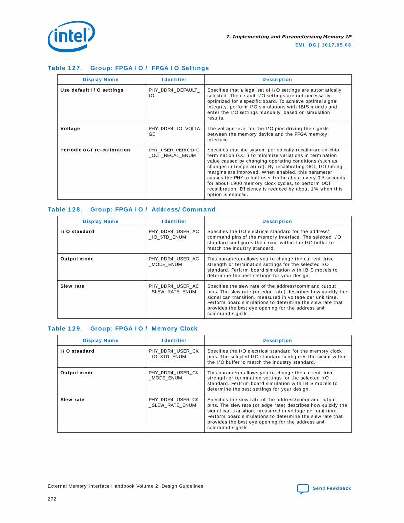
Table 127. Group: FPGA IO / FPGA IO Settings
Display Name Identifier Description
Use default I/O settings PHY_DDR4_DEFAULT_IO
Specifies that a legal set of I/O settings are automaticallyselected. The default I/O settings are not necessarilyoptimized for a specific board. To achieve optimal signalintegrity, perform I/O simulations with IBIS models andenter the I/O settings manually, based on simulationresults.
Voltage PHY_DDR4_IO_VOLTAGE
The voltage level for the I/O pins driving the signalsbetween the memory device and the FPGA memoryinterface.
Periodic OCT re-calibration PHY_USER_PERIODIC_OCT_RECAL_ENUM
Specifies that the system periodically recalibrate on-chiptermination (OCT) to minimize variations in terminationvalue caused by changing operating conditions (such aschanges in temperature). By recalibrating OCT, I/O timingmargins are improved. When enabled, this parametercauses the PHY to halt user traffic about every 0.5 secondsfor about 1900 memory clock cycles, to perform OCTrecalibration. Efficiency is reduced by about 1% when thisoption is enabled.
Table 128. Group: FPGA IO / Address/Command
Display Name Identifier Description
I/O standard PHY_DDR4_USER_AC_IO_STD_ENUM
Specifies the I/O electrical standard for the address/command pins of the memory interface. The selected I/Ostandard configures the circuit within the I/O buffer tomatch the industry standard.
Output mode PHY_DDR4_USER_AC_MODE_ENUM
This parameter allows you to change the current drivestrength or termination settings for the selected I/Ostandard. Perform board simulation with IBIS models todetermine the best settings for your design.
Slew rate PHY_DDR4_USER_AC_SLEW_RATE_ENUM
Specifies the slew rate of the address/command outputpins. The slew rate (or edge rate) describes how quickly thesignal can transition, measured in voltage per unit time.Perform board simulations to determine the slew rate thatprovides the best eye opening for the address andcommand signals.
Table 129. Group: FPGA IO / Memory Clock
Display Name Identifier Description
I/O standard PHY_DDR4_USER_CK_IO_STD_ENUM
Specifies the I/O electrical standard for the memory clockpins. The selected I/O standard configures the circuit withinthe I/O buffer to match the industry standard.
Output mode PHY_DDR4_USER_CK_MODE_ENUM
This parameter allows you to change the current drivestrength or termination settings for the selected I/Ostandard. Perform board simulation with IBIS models todetermine the best settings for your design.
Slew rate PHY_DDR4_USER_CK_SLEW_RATE_ENUM
Specifies the slew rate of the address/command outputpins. The slew rate (or edge rate) describes how quickly thesignal can transition, measured in voltage per unit time.Perform board simulations to determine the slew rate thatprovides the best eye opening for the address andcommand signals.
7. Implementing and Parameterizing Memory IP
EMI_DG | 2017.05.08
External Memory Interface Handbook Volume 2: Design Guidelines Send Feedback
272
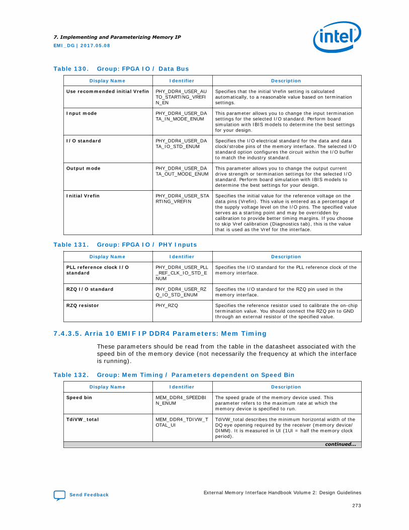
Table 130. Group: FPGA IO / Data Bus
Display Name Identifier Description
Use recommended initial Vrefin PHY_DDR4_USER_AUTO_STARTING_VREFIN_EN
Specifies that the initial Vrefin setting is calculatedautomatically, to a reasonable value based on terminationsettings.
Input mode PHY_DDR4_USER_DATA_IN_MODE_ENUM
This parameter allows you to change the input terminationsettings for the selected I/O standard. Perform boardsimulation with IBIS models to determine the best settingsfor your design.
I/O standard PHY_DDR4_USER_DATA_IO_STD_ENUM
Specifies the I/O electrical standard for the data and dataclock/strobe pins of the memory interface. The selected I/Ostandard option configures the circuit within the I/O bufferto match the industry standard.
Output mode PHY_DDR4_USER_DATA_OUT_MODE_ENUM
This parameter allows you to change the output currentdrive strength or termination settings for the selected I/Ostandard. Perform board simulation with IBIS models todetermine the best settings for your design.
Initial Vrefin PHY_DDR4_USER_STARTING_VREFIN
Specifies the initial value for the reference voltage on thedata pins (Vrefin). This value is entered as a percentage ofthe supply voltage level on the I/O pins. The specified valueserves as a starting point and may be overridden bycalibration to provide better timing margins. If you chooseto skip Vref calibration (Diagnostics tab), this is the valuethat is used as the Vref for the interface.
Table 131. Group: FPGA IO / PHY Inputs
Display Name Identifier Description
PLL reference clock I/Ostandard
PHY_DDR4_USER_PLL_REF_CLK_IO_STD_ENUM
Specifies the I/O standard for the PLL reference clock of thememory interface.
RZQ I/O standard PHY_DDR4_USER_RZQ_IO_STD_ENUM
Specifies the I/O standard for the RZQ pin used in thememory interface.
RZQ resistor PHY_RZQ Specifies the reference resistor used to calibrate the on-chiptermination value. You should connect the RZQ pin to GNDthrough an external resistor of the specified value.
7.4.3.5. Arria 10 EMIF IP DDR4 Parameters: Mem Timing
These parameters should be read from the table in the datasheet associated with thespeed bin of the memory device (not necessarily the frequency at which the interfaceis running).
Table 132. Group: Mem Timing / Parameters dependent on Speed Bin
Display Name Identifier Description
Speed bin MEM_DDR4_SPEEDBIN_ENUM
The speed grade of the memory device used. Thisparameter refers to the maximum rate at which thememory device is specified to run.
TdiVW_total MEM_DDR4_TDIVW_TOTAL_UI
TdiVW_total describes the minimum horizontal width of theDQ eye opening required by the receiver (memory device/DIMM). It is measured in UI (1UI = half the memory clockperiod).
continued...
7. Implementing and Parameterizing Memory IP
EMI_DG | 2017.05.08
Send Feedback External Memory Interface Handbook Volume 2: Design Guidelines
273
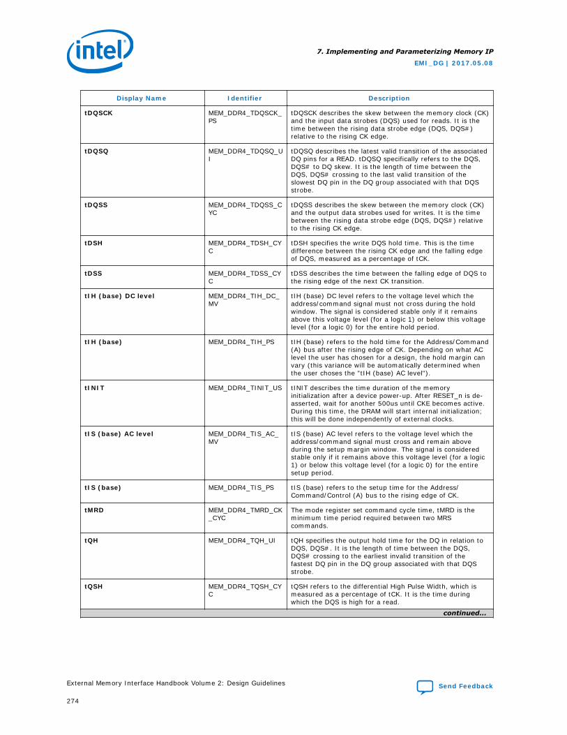
Display Name Identifier Description
tDQSCK MEM_DDR4_TDQSCK_PS
tDQSCK describes the skew between the memory clock (CK)and the input data strobes (DQS) used for reads. It is thetime between the rising data strobe edge (DQS, DQS#)relative to the rising CK edge.
tDQSQ MEM_DDR4_TDQSQ_UI
tDQSQ describes the latest valid transition of the associatedDQ pins for a READ. tDQSQ specifically refers to the DQS,DQS# to DQ skew. It is the length of time between theDQS, DQS# crossing to the last valid transition of theslowest DQ pin in the DQ group associated with that DQSstrobe.
tDQSS MEM_DDR4_TDQSS_CYC
tDQSS describes the skew between the memory clock (CK)and the output data strobes used for writes. It is the timebetween the rising data strobe edge (DQS, DQS#) relativeto the rising CK edge.
tDSH MEM_DDR4_TDSH_CYC
tDSH specifies the write DQS hold time. This is the timedifference between the rising CK edge and the falling edgeof DQS, measured as a percentage of tCK.
tDSS MEM_DDR4_TDSS_CYC
tDSS describes the time between the falling edge of DQS tothe rising edge of the next CK transition.
tIH (base) DC level MEM_DDR4_TIH_DC_MV
tIH (base) DC level refers to the voltage level which theaddress/command signal must not cross during the holdwindow. The signal is considered stable only if it remainsabove this voltage level (for a logic 1) or below this voltagelevel (for a logic 0) for the entire hold period.
tIH (base) MEM_DDR4_TIH_PS tIH (base) refers to the hold time for the Address/Command(A) bus after the rising edge of CK. Depending on what AClevel the user has chosen for a design, the hold margin canvary (this variance will be automatically determined whenthe user choses the "tIH (base) AC level").
tINIT MEM_DDR4_TINIT_US tINIT describes the time duration of the memoryinitialization after a device power-up. After RESET_n is de-asserted, wait for another 500us until CKE becomes active.During this time, the DRAM will start internal initialization;this will be done independently of external clocks.
tIS (base) AC level MEM_DDR4_TIS_AC_MV
tIS (base) AC level refers to the voltage level which theaddress/command signal must cross and remain aboveduring the setup margin window. The signal is consideredstable only if it remains above this voltage level (for a logic1) or below this voltage level (for a logic 0) for the entiresetup period.
tIS (base) MEM_DDR4_TIS_PS tIS (base) refers to the setup time for the Address/Command/Control (A) bus to the rising edge of CK.
tMRD MEM_DDR4_TMRD_CK_CYC
The mode register set command cycle time, tMRD is theminimum time period required between two MRScommands.
tQH MEM_DDR4_TQH_UI tQH specifies the output hold time for the DQ in relation toDQS, DQS#. It is the length of time between the DQS,DQS# crossing to the earliest invalid transition of thefastest DQ pin in the DQ group associated with that DQSstrobe.
tQSH MEM_DDR4_TQSH_CYC
tQSH refers to the differential High Pulse Width, which ismeasured as a percentage of tCK. It is the time duringwhich the DQS is high for a read.
continued...
7. Implementing and Parameterizing Memory IP
EMI_DG | 2017.05.08
External Memory Interface Handbook Volume 2: Design Guidelines Send Feedback
274
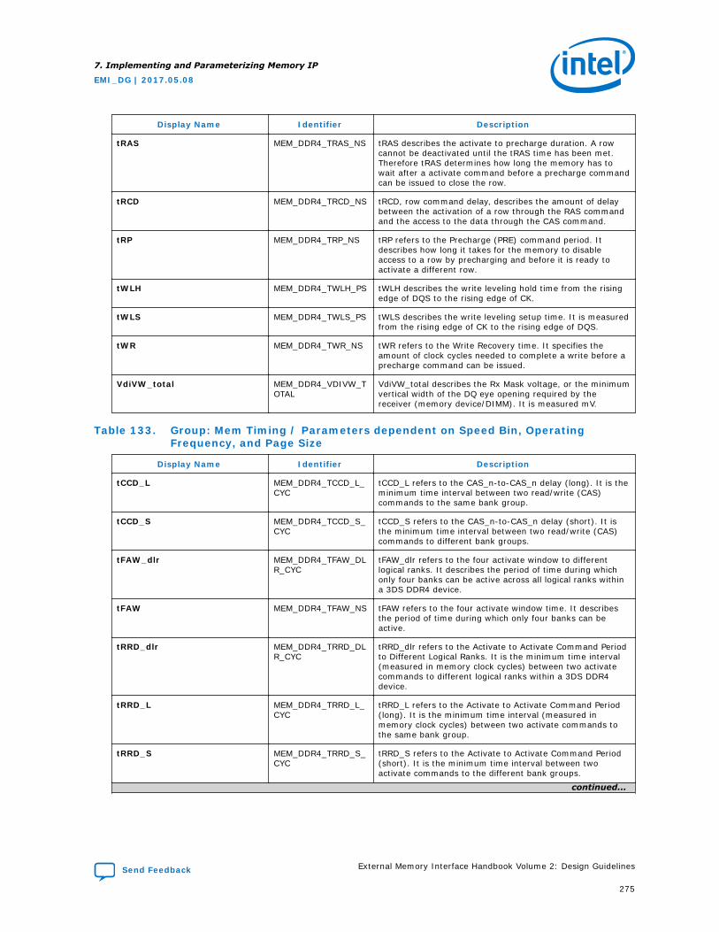
Display Name Identifier Description
tRAS MEM_DDR4_TRAS_NS tRAS describes the activate to precharge duration. A rowcannot be deactivated until the tRAS time has been met.Therefore tRAS determines how long the memory has towait after a activate command before a precharge commandcan be issued to close the row.
tRCD MEM_DDR4_TRCD_NS tRCD, row command delay, describes the amount of delaybetween the activation of a row through the RAS commandand the access to the data through the CAS command.
tRP MEM_DDR4_TRP_NS tRP refers to the Precharge (PRE) command period. Itdescribes how long it takes for the memory to disableaccess to a row by precharging and before it is ready toactivate a different row.
tWLH MEM_DDR4_TWLH_PS tWLH describes the write leveling hold time from the risingedge of DQS to the rising edge of CK.
tWLS MEM_DDR4_TWLS_PS tWLS describes the write leveling setup time. It is measuredfrom the rising edge of CK to the rising edge of DQS.
tWR MEM_DDR4_TWR_NS tWR refers to the Write Recovery time. It specifies theamount of clock cycles needed to complete a write before aprecharge command can be issued.
VdiVW_total MEM_DDR4_VDIVW_TOTAL
VdiVW_total describes the Rx Mask voltage, or the minimumvertical width of the DQ eye opening required by thereceiver (memory device/DIMM). It is measured mV.
Table 133. Group: Mem Timing / Parameters dependent on Speed Bin, OperatingFrequency, and Page Size
Display Name Identifier Description
tCCD_L MEM_DDR4_TCCD_L_CYC
tCCD_L refers to the CAS_n-to-CAS_n delay (long). It is theminimum time interval between two read/write (CAS)commands to the same bank group.
tCCD_S MEM_DDR4_TCCD_S_CYC
tCCD_S refers to the CAS_n-to-CAS_n delay (short). It isthe minimum time interval between two read/write (CAS)commands to different bank groups.
tFAW_dlr MEM_DDR4_TFAW_DLR_CYC
tFAW_dlr refers to the four activate window to differentlogical ranks. It describes the period of time during whichonly four banks can be active across all logical ranks withina 3DS DDR4 device.
tFAW MEM_DDR4_TFAW_NS tFAW refers to the four activate window time. It describesthe period of time during which only four banks can beactive.
tRRD_dlr MEM_DDR4_TRRD_DLR_CYC
tRRD_dlr refers to the Activate to Activate Command Periodto Different Logical Ranks. It is the minimum time interval(measured in memory clock cycles) between two activatecommands to different logical ranks within a 3DS DDR4device.
tRRD_L MEM_DDR4_TRRD_L_CYC
tRRD_L refers to the Activate to Activate Command Period(long). It is the minimum time interval (measured inmemory clock cycles) between two activate commands tothe same bank group.
tRRD_S MEM_DDR4_TRRD_S_CYC
tRRD_S refers to the Activate to Activate Command Period(short). It is the minimum time interval between twoactivate commands to the different bank groups.
continued...
7. Implementing and Parameterizing Memory IP
EMI_DG | 2017.05.08
Send Feedback External Memory Interface Handbook Volume 2: Design Guidelines
275
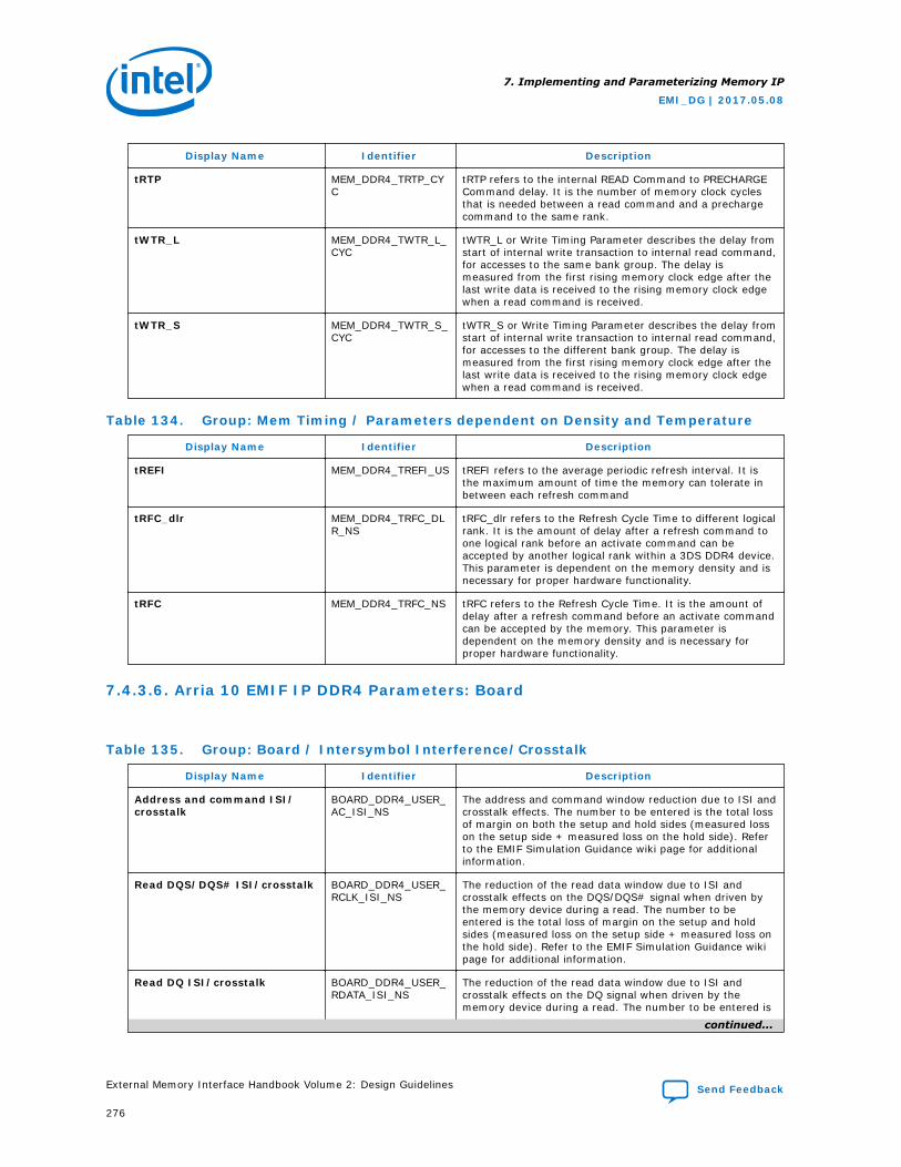
Display Name Identifier Description
tRTP MEM_DDR4_TRTP_CYC
tRTP refers to the internal READ Command to PRECHARGECommand delay. It is the number of memory clock cyclesthat is needed between a read command and a prechargecommand to the same rank.
tWTR_L MEM_DDR4_TWTR_L_CYC
tWTR_L or Write Timing Parameter describes the delay fromstart of internal write transaction to internal read command,for accesses to the same bank group. The delay ismeasured from the first rising memory clock edge after thelast write data is received to the rising memory clock edgewhen a read command is received.
tWTR_S MEM_DDR4_TWTR_S_CYC
tWTR_S or Write Timing Parameter describes the delay fromstart of internal write transaction to internal read command,for accesses to the different bank group. The delay ismeasured from the first rising memory clock edge after thelast write data is received to the rising memory clock edgewhen a read command is received.
Table 134. Group: Mem Timing / Parameters dependent on Density and Temperature
Display Name Identifier Description
tREFI MEM_DDR4_TREFI_US tREFI refers to the average periodic refresh interval. It isthe maximum amount of time the memory can tolerate inbetween each refresh command
tRFC_dlr MEM_DDR4_TRFC_DLR_NS
tRFC_dlr refers to the Refresh Cycle Time to different logicalrank. It is the amount of delay after a refresh command toone logical rank before an activate command can beaccepted by another logical rank within a 3DS DDR4 device.This parameter is dependent on the memory density and isnecessary for proper hardware functionality.
tRFC MEM_DDR4_TRFC_NS tRFC refers to the Refresh Cycle Time. It is the amount ofdelay after a refresh command before an activate commandcan be accepted by the memory. This parameter isdependent on the memory density and is necessary forproper hardware functionality.
7.4.3.6. Arria 10 EMIF IP DDR4 Parameters: Board
Table 135. Group: Board / Intersymbol Interference/Crosstalk
Display Name Identifier Description
Address and command ISI/crosstalk
BOARD_DDR4_USER_AC_ISI_NS
The address and command window reduction due to ISI andcrosstalk effects. The number to be entered is the total lossof margin on both the setup and hold sides (measured losson the setup side + measured loss on the hold side). Referto the EMIF Simulation Guidance wiki page for additionalinformation.
Read DQS/DQS# ISI/crosstalk BOARD_DDR4_USER_RCLK_ISI_NS
The reduction of the read data window due to ISI andcrosstalk effects on the DQS/DQS# signal when driven bythe memory device during a read. The number to beentered is the total loss of margin on the setup and holdsides (measured loss on the setup side + measured loss onthe hold side). Refer to the EMIF Simulation Guidance wikipage for additional information.
Read DQ ISI/crosstalk BOARD_DDR4_USER_RDATA_ISI_NS
The reduction of the read data window due to ISI andcrosstalk effects on the DQ signal when driven by thememory device during a read. The number to be entered is
continued...
7. Implementing and Parameterizing Memory IP
EMI_DG | 2017.05.08
External Memory Interface Handbook Volume 2: Design Guidelines Send Feedback
276
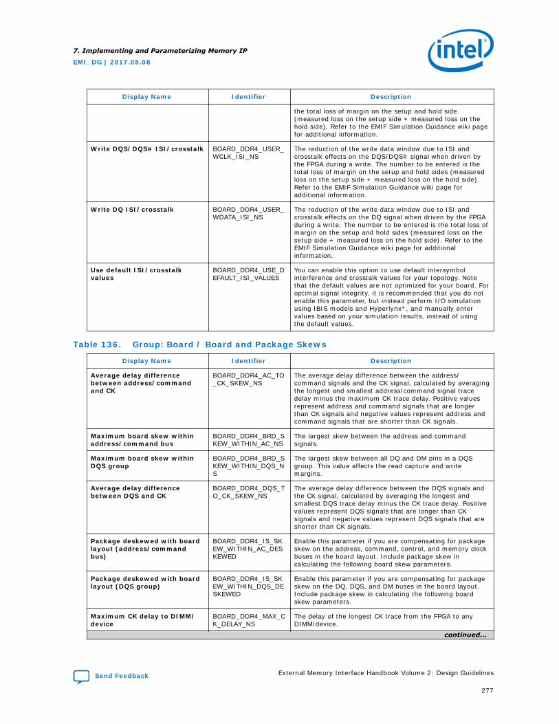
Display Name Identifier Description
the total loss of margin on the setup and hold side(measured loss on the setup side + measured loss on thehold side). Refer to the EMIF Simulation Guidance wiki pagefor additional information.
Write DQS/DQS# ISI/crosstalk BOARD_DDR4_USER_WCLK_ISI_NS
The reduction of the write data window due to ISI andcrosstalk effects on the DQS/DQS# signal when driven bythe FPGA during a write. The number to be entered is thetotal loss of margin on the setup and hold sides (measuredloss on the setup side + measured loss on the hold side).Refer to the EMIF Simulation Guidance wiki page foradditional information.
Write DQ ISI/crosstalk BOARD_DDR4_USER_WDATA_ISI_NS
The reduction of the write data window due to ISI andcrosstalk effects on the DQ signal when driven by the FPGAduring a write. The number to be entered is the total loss ofmargin on the setup and hold sides (measured loss on thesetup side + measured loss on the hold side). Refer to theEMIF Simulation Guidance wiki page for additionalinformation.
Use default ISI/crosstalkvalues
BOARD_DDR4_USE_DEFAULT_ISI_VALUES
You can enable this option to use default intersymbolinterference and crosstalk values for your topology. Notethat the default values are not optimized for your board. Foroptimal signal integrity, it is recommended that you do notenable this parameter, but instead perform I/O simulationusing IBIS models and Hyperlynx*, and manually entervalues based on your simulation results, instead of usingthe default values.
Table 136. Group: Board / Board and Package Skews
Display Name Identifier Description
Average delay differencebetween address/commandand CK
BOARD_DDR4_AC_TO_CK_SKEW_NS
The average delay difference between the address/command signals and the CK signal, calculated by averagingthe longest and smallest address/command signal tracedelay minus the maximum CK trace delay. Positive valuesrepresent address and command signals that are longerthan CK signals and negative values represent address andcommand signals that are shorter than CK signals.
Maximum board skew withinaddress/command bus
BOARD_DDR4_BRD_SKEW_WITHIN_AC_NS
The largest skew between the address and commandsignals.
Maximum board skew withinDQS group
BOARD_DDR4_BRD_SKEW_WITHIN_DQS_NS
The largest skew between all DQ and DM pins in a DQSgroup. This value affects the read capture and writemargins.
Average delay differencebetween DQS and CK
BOARD_DDR4_DQS_TO_CK_SKEW_NS
The average delay difference between the DQS signals andthe CK signal, calculated by averaging the longest andsmallest DQS trace delay minus the CK trace delay. Positivevalues represent DQS signals that are longer than CKsignals and negative values represent DQS signals that areshorter than CK signals.
Package deskewed with boardlayout (address/commandbus)
BOARD_DDR4_IS_SKEW_WITHIN_AC_DESKEWED
Enable this parameter if you are compensating for packageskew on the address, command, control, and memory clockbuses in the board layout. Include package skew incalculating the following board skew parameters.
Package deskewed with boardlayout (DQS group)
BOARD_DDR4_IS_SKEW_WITHIN_DQS_DESKEWED
Enable this parameter if you are compensating for packageskew on the DQ, DQS, and DM buses in the board layout.Include package skew in calculating the following boardskew parameters.
Maximum CK delay to DIMM/device
BOARD_DDR4_MAX_CK_DELAY_NS
The delay of the longest CK trace from the FPGA to anyDIMM/device.
continued...
7. Implementing and Parameterizing Memory IP
EMI_DG | 2017.05.08
Send Feedback External Memory Interface Handbook Volume 2: Design Guidelines
277
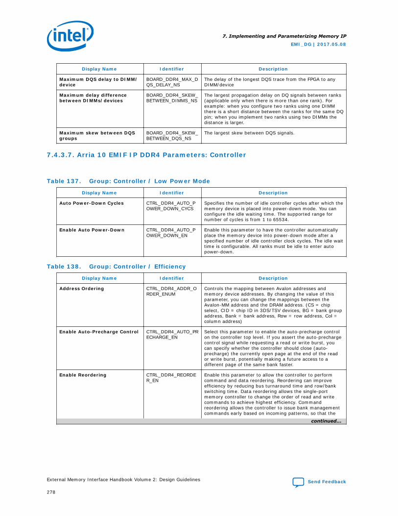
Display Name Identifier Description
Maximum DQS delay to DIMM/device
BOARD_DDR4_MAX_DQS_DELAY_NS
The delay of the longest DQS trace from the FPGA to anyDIMM/device
Maximum delay differencebetween DIMMs/devices
BOARD_DDR4_SKEW_BETWEEN_DIMMS_NS
The largest propagation delay on DQ signals between ranks(applicable only when there is more than one rank). Forexample: when you configure two ranks using one DIMMthere is a short distance between the ranks for the same DQpin; when you implement two ranks using two DIMMs thedistance is larger.
Maximum skew between DQSgroups
BOARD_DDR4_SKEW_BETWEEN_DQS_NS
The largest skew between DQS signals.
7.4.3.7. Arria 10 EMIF IP DDR4 Parameters: Controller
Table 137. Group: Controller / Low Power Mode
Display Name Identifier Description
Auto Power-Down Cycles CTRL_DDR4_AUTO_POWER_DOWN_CYCS
Specifies the number of idle controller cycles after which thememory device is placed into power-down mode. You canconfigure the idle waiting time. The supported range fornumber of cycles is from 1 to 65534.
Enable Auto Power-Down CTRL_DDR4_AUTO_POWER_DOWN_EN
Enable this parameter to have the controller automaticallyplace the memory device into power-down mode after aspecified number of idle controller clock cycles. The idle waittime is configurable. All ranks must be idle to enter autopower-down.
Table 138. Group: Controller / Efficiency
Display Name Identifier Description
Address Ordering CTRL_DDR4_ADDR_ORDER_ENUM
Controls the mapping between Avalon addresses andmemory device addresses. By changing the value of thisparameter, you can change the mappings between theAvalon-MM address and the DRAM address. (CS = chipselect, CID = chip ID in 3DS/TSV devices, BG = bank groupaddress, Bank = bank address, Row = row address, Col =column address)
Enable Auto-Precharge Control CTRL_DDR4_AUTO_PRECHARGE_EN
Select this parameter to enable the auto-precharge controlon the controller top level. If you assert the auto-prechargecontrol signal while requesting a read or write burst, youcan specify whether the controller should close (auto-precharge) the currently open page at the end of the reador write burst, potentially making a future access to adifferent page of the same bank faster.
Enable Reordering CTRL_DDR4_REORDER_EN
Enable this parameter to allow the controller to performcommand and data reordering. Reordering can improveefficiency by reducing bus turnaround time and row/bankswitching time. Data reordering allows the single-portmemory controller to change the order of read and writecommands to achieve highest efficiency. Commandreordering allows the controller to issue bank managementcommands early based on incoming patterns, so that the
continued...
7. Implementing and Parameterizing Memory IP
EMI_DG | 2017.05.08
External Memory Interface Handbook Volume 2: Design Guidelines Send Feedback
278
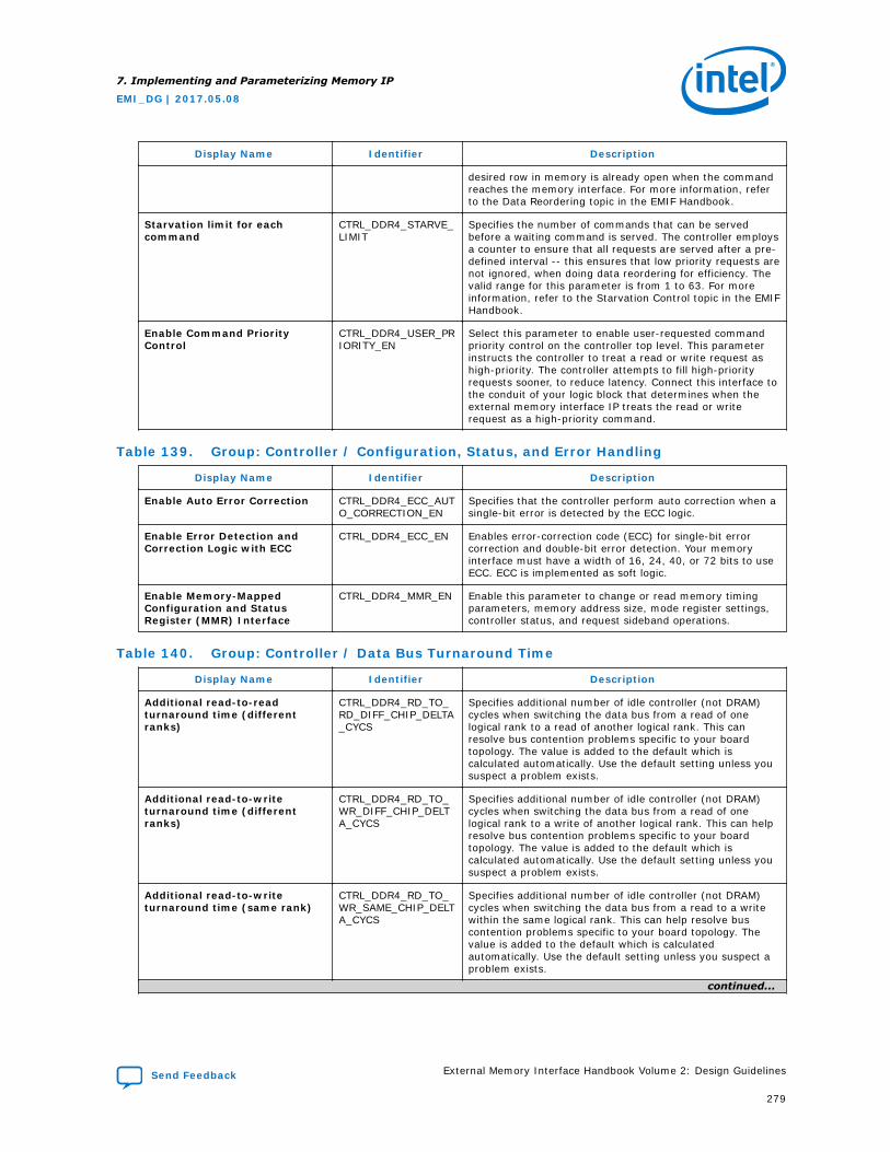
Display Name Identifier Description
desired row in memory is already open when the commandreaches the memory interface. For more information, referto the Data Reordering topic in the EMIF Handbook.
Starvation limit for eachcommand
CTRL_DDR4_STARVE_LIMIT
Specifies the number of commands that can be servedbefore a waiting command is served. The controller employsa counter to ensure that all requests are served after a pre-defined interval -- this ensures that low priority requests arenot ignored, when doing data reordering for efficiency. Thevalid range for this parameter is from 1 to 63. For moreinformation, refer to the Starvation Control topic in the EMIFHandbook.
Enable Command PriorityControl
CTRL_DDR4_USER_PRIORITY_EN
Select this parameter to enable user-requested commandpriority control on the controller top level. This parameterinstructs the controller to treat a read or write request ashigh-priority. The controller attempts to fill high-priorityrequests sooner, to reduce latency. Connect this interface tothe conduit of your logic block that determines when theexternal memory interface IP treats the read or writerequest as a high-priority command.
Table 139. Group: Controller / Configuration, Status, and Error Handling
Display Name Identifier Description
Enable Auto Error Correction CTRL_DDR4_ECC_AUTO_CORRECTION_EN
Specifies that the controller perform auto correction when asingle-bit error is detected by the ECC logic.
Enable Error Detection andCorrection Logic with ECC
CTRL_DDR4_ECC_EN Enables error-correction code (ECC) for single-bit errorcorrection and double-bit error detection. Your memoryinterface must have a width of 16, 24, 40, or 72 bits to useECC. ECC is implemented as soft logic.
Enable Memory-MappedConfiguration and StatusRegister (MMR) Interface
CTRL_DDR4_MMR_EN Enable this parameter to change or read memory timingparameters, memory address size, mode register settings,controller status, and request sideband operations.
Table 140. Group: Controller / Data Bus Turnaround Time
Display Name Identifier Description
Additional read-to-readturnaround time (differentranks)
CTRL_DDR4_RD_TO_RD_DIFF_CHIP_DELTA_CYCS
Specifies additional number of idle controller (not DRAM)cycles when switching the data bus from a read of onelogical rank to a read of another logical rank. This canresolve bus contention problems specific to your boardtopology. The value is added to the default which iscalculated automatically. Use the default setting unless yoususpect a problem exists.
Additional read-to-writeturnaround time (differentranks)
CTRL_DDR4_RD_TO_WR_DIFF_CHIP_DELTA_CYCS
Specifies additional number of idle controller (not DRAM)cycles when switching the data bus from a read of onelogical rank to a write of another logical rank. This can helpresolve bus contention problems specific to your boardtopology. The value is added to the default which iscalculated automatically. Use the default setting unless yoususpect a problem exists.
Additional read-to-writeturnaround time (same rank)
CTRL_DDR4_RD_TO_WR_SAME_CHIP_DELTA_CYCS
Specifies additional number of idle controller (not DRAM)cycles when switching the data bus from a read to a writewithin the same logical rank. This can help resolve buscontention problems specific to your board topology. Thevalue is added to the default which is calculatedautomatically. Use the default setting unless you suspect aproblem exists.
continued...
7. Implementing and Parameterizing Memory IP
EMI_DG | 2017.05.08
Send Feedback External Memory Interface Handbook Volume 2: Design Guidelines
279
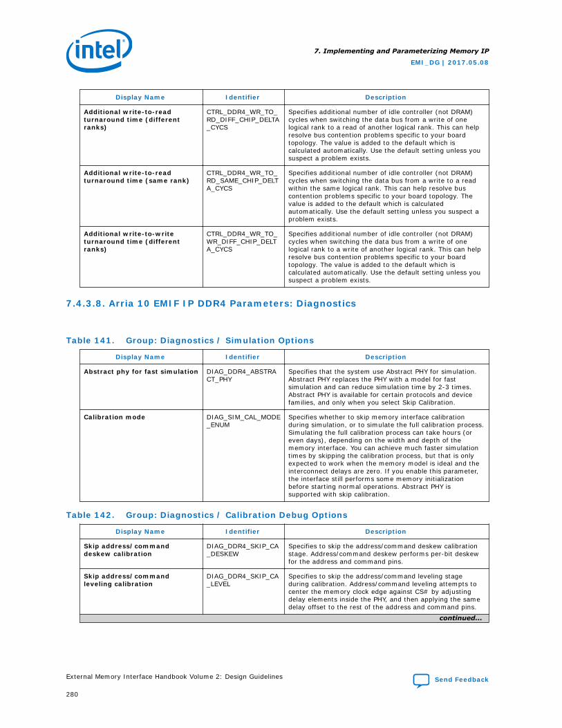
Display Name Identifier Description
Additional write-to-readturnaround time (differentranks)
CTRL_DDR4_WR_TO_RD_DIFF_CHIP_DELTA_CYCS
Specifies additional number of idle controller (not DRAM)cycles when switching the data bus from a write of onelogical rank to a read of another logical rank. This can helpresolve bus contention problems specific to your boardtopology. The value is added to the default which iscalculated automatically. Use the default setting unless yoususpect a problem exists.
Additional write-to-readturnaround time (same rank)
CTRL_DDR4_WR_TO_RD_SAME_CHIP_DELTA_CYCS
Specifies additional number of idle controller (not DRAM)cycles when switching the data bus from a write to a readwithin the same logical rank. This can help resolve buscontention problems specific to your board topology. Thevalue is added to the default which is calculatedautomatically. Use the default setting unless you suspect aproblem exists.
Additional write-to-writeturnaround time (differentranks)
CTRL_DDR4_WR_TO_WR_DIFF_CHIP_DELTA_CYCS
Specifies additional number of idle controller (not DRAM)cycles when switching the data bus from a write of onelogical rank to a write of another logical rank. This can helpresolve bus contention problems specific to your boardtopology. The value is added to the default which iscalculated automatically. Use the default setting unless yoususpect a problem exists.
7.4.3.8. Arria 10 EMIF IP DDR4 Parameters: Diagnostics
Table 141. Group: Diagnostics / Simulation Options
Display Name Identifier Description
Abstract phy for fast simulation DIAG_DDR4_ABSTRACT_PHY
Specifies that the system use Abstract PHY for simulation.Abstract PHY replaces the PHY with a model for fastsimulation and can reduce simulation time by 2-3 times.Abstract PHY is available for certain protocols and devicefamilies, and only when you select Skip Calibration.
Calibration mode DIAG_SIM_CAL_MODE_ENUM
Specifies whether to skip memory interface calibrationduring simulation, or to simulate the full calibration process.Simulating the full calibration process can take hours (oreven days), depending on the width and depth of thememory interface. You can achieve much faster simulationtimes by skipping the calibration process, but that is onlyexpected to work when the memory model is ideal and theinterconnect delays are zero. If you enable this parameter,the interface still performs some memory initializationbefore starting normal operations. Abstract PHY issupported with skip calibration.
Table 142. Group: Diagnostics / Calibration Debug Options
Display Name Identifier Description
Skip address/commanddeskew calibration
DIAG_DDR4_SKIP_CA_DESKEW
Specifies to skip the address/command deskew calibrationstage. Address/command deskew performs per-bit deskewfor the address and command pins.
Skip address/commandleveling calibration
DIAG_DDR4_SKIP_CA_LEVEL
Specifies to skip the address/command leveling stageduring calibration. Address/command leveling attempts tocenter the memory clock edge against CS# by adjustingdelay elements inside the PHY, and then applying the samedelay offset to the rest of the address and command pins.
continued...
7. Implementing and Parameterizing Memory IP
EMI_DG | 2017.05.08
External Memory Interface Handbook Volume 2: Design Guidelines Send Feedback
280
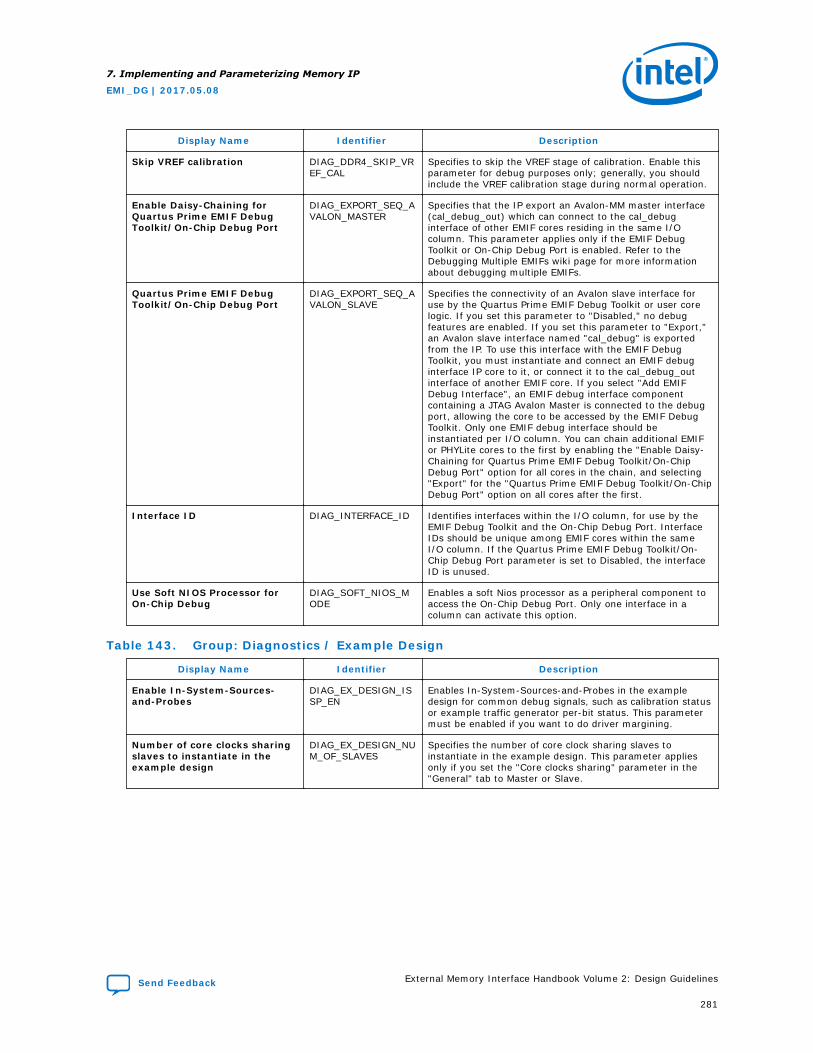
Display Name Identifier Description
Skip VREF calibration DIAG_DDR4_SKIP_VREF_CAL
Specifies to skip the VREF stage of calibration. Enable thisparameter for debug purposes only; generally, you shouldinclude the VREF calibration stage during normal operation.
Enable Daisy-Chaining forQuartus Prime EMIF DebugToolkit/On-Chip Debug Port
DIAG_EXPORT_SEQ_AVALON_MASTER
Specifies that the IP export an Avalon-MM master interface(cal_debug_out) which can connect to the cal_debuginterface of other EMIF cores residing in the same I/Ocolumn. This parameter applies only if the EMIF DebugToolkit or On-Chip Debug Port is enabled. Refer to theDebugging Multiple EMIFs wiki page for more informationabout debugging multiple EMIFs.
Quartus Prime EMIF DebugToolkit/On-Chip Debug Port
DIAG_EXPORT_SEQ_AVALON_SLAVE
Specifies the connectivity of an Avalon slave interface foruse by the Quartus Prime EMIF Debug Toolkit or user corelogic. If you set this parameter to "Disabled," no debugfeatures are enabled. If you set this parameter to "Export,"an Avalon slave interface named "cal_debug" is exportedfrom the IP. To use this interface with the EMIF DebugToolkit, you must instantiate and connect an EMIF debuginterface IP core to it, or connect it to the cal_debug_outinterface of another EMIF core. If you select "Add EMIFDebug Interface", an EMIF debug interface componentcontaining a JTAG Avalon Master is connected to the debugport, allowing the core to be accessed by the EMIF DebugToolkit. Only one EMIF debug interface should beinstantiated per I/O column. You can chain additional EMIFor PHYLite cores to the first by enabling the "Enable Daisy-Chaining for Quartus Prime EMIF Debug Toolkit/On-ChipDebug Port" option for all cores in the chain, and selecting"Export" for the "Quartus Prime EMIF Debug Toolkit/On-ChipDebug Port" option on all cores after the first.
Interface ID DIAG_INTERFACE_ID Identifies interfaces within the I/O column, for use by theEMIF Debug Toolkit and the On-Chip Debug Port. InterfaceIDs should be unique among EMIF cores within the sameI/O column. If the Quartus Prime EMIF Debug Toolkit/On-Chip Debug Port parameter is set to Disabled, the interfaceID is unused.
Use Soft NIOS Processor forOn-Chip Debug
DIAG_SOFT_NIOS_MODE
Enables a soft Nios processor as a peripheral component toaccess the On-Chip Debug Port. Only one interface in acolumn can activate this option.
Table 143. Group: Diagnostics / Example Design
Display Name Identifier Description
Enable In-System-Sources-and-Probes
DIAG_EX_DESIGN_ISSP_EN
Enables In-System-Sources-and-Probes in the exampledesign for common debug signals, such as calibration statusor example traffic generator per-bit status. This parametermust be enabled if you want to do driver margining.
Number of core clocks sharingslaves to instantiate in theexample design
DIAG_EX_DESIGN_NUM_OF_SLAVES
Specifies the number of core clock sharing slaves toinstantiate in the example design. This parameter appliesonly if you set the "Core clocks sharing" parameter in the"General" tab to Master or Slave.
7. Implementing and Parameterizing Memory IP
EMI_DG | 2017.05.08
Send Feedback External Memory Interface Handbook Volume 2: Design Guidelines
281
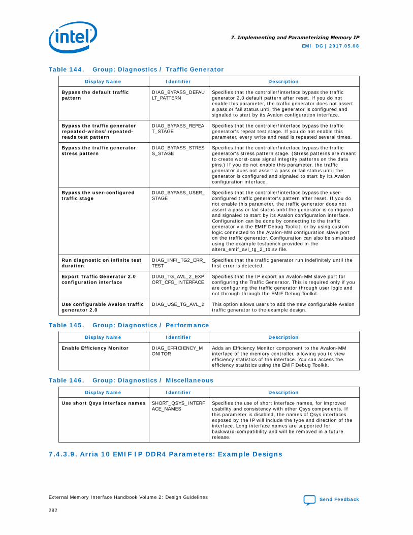
Table 144. Group: Diagnostics / Traffic Generator
Display Name Identifier Description
Bypass the default trafficpattern
DIAG_BYPASS_DEFAULT_PATTERN
Specifies that the controller/interface bypass the trafficgenerator 2.0 default pattern after reset. If you do notenable this parameter, the traffic generator does not asserta pass or fail status until the generator is configured andsignaled to start by its Avalon configuration interface.
Bypass the traffic generatorrepeated-writes/repeated-reads test pattern
DIAG_BYPASS_REPEAT_STAGE
Specifies that the controller/interface bypass the trafficgenerator's repeat test stage. If you do not enable thisparameter, every write and read is repeated several times.
Bypass the traffic generatorstress pattern
DIAG_BYPASS_STRESS_STAGE
Specifies that the controller/interface bypass the trafficgenerator's stress pattern stage. (Stress patterns are meantto create worst-case signal integrity patterns on the datapins.) If you do not enable this parameter, the trafficgenerator does not assert a pass or fail status until thegenerator is configured and signaled to start by its Avalonconfiguration interface.
Bypass the user-configuredtraffic stage
DIAG_BYPASS_USER_STAGE
Specifies that the controller/interface bypass the user-configured traffic generator's pattern after reset. If you donot enable this parameter, the traffic generator does notassert a pass or fail status until the generator is configuredand signaled to start by its Avalon configuration interface.Configuration can be done by connecting to the trafficgenerator via the EMIF Debug Toolkit, or by using customlogic connected to the Avalon-MM configuration slave porton the traffic generator. Configuration can also be simulatedusing the example testbench provided in thealtera_emif_avl_tg_2_tb.sv file.
Run diagnostic on infinite testduration
DIAG_INFI_TG2_ERR_TEST
Specifies that the traffic generator run indefinitely until thefirst error is detected.
Export Traffic Generator 2.0configuration interface
DIAG_TG_AVL_2_EXPORT_CFG_INTERFACE
Specifies that the IP export an Avalon-MM slave port forconfiguring the Traffic Generator. This is required only if youare configuring the traffic generator through user logic andnot through through the EMIF Debug Toolkit.
Use configurable Avalon trafficgenerator 2.0
DIAG_USE_TG_AVL_2 This option allows users to add the new configurable Avalontraffic generator to the example design.
Table 145. Group: Diagnostics / Performance
Display Name Identifier Description
Enable Efficiency Monitor DIAG_EFFICIENCY_MONITOR
Adds an Efficiency Monitor component to the Avalon-MMinterface of the memory controller, allowing you to viewefficiency statistics of the interface. You can access theefficiency statistics using the EMIF Debug Toolkit.
Table 146. Group: Diagnostics / Miscellaneous
Display Name Identifier Description
Use short Qsys interface names SHORT_QSYS_INTERFACE_NAMES
Specifies the use of short interface names, for improvedusability and consistency with other Qsys components. Ifthis parameter is disabled, the names of Qsys interfacesexposed by the IP will include the type and direction of theinterface. Long interface names are supported forbackward-compatibility and will be removed in a futurerelease.
7.4.3.9. Arria 10 EMIF IP DDR4 Parameters: Example Designs
7. Implementing and Parameterizing Memory IP
EMI_DG | 2017.05.08
External Memory Interface Handbook Volume 2: Design Guidelines Send Feedback
282

Table 147. Group: Example Designs / Available Example Designs
Display Name Identifier Description
Select design EX_DESIGN_GUI_DDR4_SEL_DESIGN
Specifies the creation of a full Quartus Prime project,instantiating an external memory interface and an exampletraffic generator, according to your parameterization. Afterthe design is created, you can specify the target device andpin location assignments, run a full compilation, verifytiming closure, and test the interface on your board usingthe programming file created by the Quartus Primeassembler. The 'Generate Example Design' button lets yougenerate simulation or synthesis file sets.
Table 148. Group: Example Designs / Example Design Files
Display Name Identifier Description
Simulation EX_DESIGN_GUI_DDR4_GEN_SIM
Specifies that the 'Generate Example Design' button createall necessary file sets for simulation. Expect a shortadditional delay as the file set is created. If you do notenable this parameter, simulation file sets are not created.Instead, the output directory will contain the ed_sim.qsysfile which holds Qsys details of the simulation exampledesign, and a make_sim_design.tcl file with othercorresponding tcl files. You can run make_sim_design.tclfrom a command line to generate the simulation exampledesign. The generated example designs for varioussimulators are stored in the /sim sub-directory.
Synthesis EX_DESIGN_GUI_DDR4_GEN_SYNTH
Specifies that the 'Generate Example Design' button createall necessary file sets for synthesis. Expect a shortadditional delay as the file set is created. If you do notenable this parameter, synthesis file sets are not created.Instead, the output directory will contain the ed_synth.qsysfile which holds Qsys details of the synthesis exampledesign, and a make_qii_design.tcl script with othercorresponding tcl files. You can run make_qii_design.tclfrom a command line to generate the synthesis exampledesign. The generated example design is stored in the /qiisub-directory.
Table 149. Group: Example Designs / Generated HDL Format
Display Name Identifier Description
Simulation HDL format EX_DESIGN_GUI_DDR4_HDL_FORMAT
This option lets you choose the format of HDL in whichgenerated simulation files are created.
Table 150. Group: Example Designs / Target Development Kit
Display Name Identifier Description
Select board EX_DESIGN_GUI_DDR4_TARGET_DEV_KIT
Specifies that when you select a development kit with amemory module, the generated example design contains allsettings and fixed pin assignments to run on the selectedboard. You must select a development kit preset togenerate a working example design for the specifieddevelopment kit. Any IP settings not applied directly from adevelopment kit preset will not have guaranteed resultswhen testing the development kit. To exclude hardwaresupport of the example design, select 'none' from the'Select board' pull down menu. When you apply adevelopment kit preset, all IP parameters are automaticallyset appropriately to match the selected preset. If you wantto save your current settings, you should do so before youapply the preset. You can save your settings under adifferent name using File->Save as.
7. Implementing and Parameterizing Memory IP
EMI_DG | 2017.05.08
Send Feedback External Memory Interface Handbook Volume 2: Design Guidelines
283
7.4.3.10. About Memory Presets
Presets help simplify the process of copying memory parameter values from memorydevice data sheets to the EMIF parameter editor.
For DDRx protocols, the memory presets are named using the following convention:
PROTOCOL-SPEEDBIN LATENCY FORMAT-AND-TOPOLOGY CAPACITY (INTERNAL-ORGANIZATION)
For example, the preset named DDR4-2666U CL18 Component 1CS 2Gb (512Mbx 4) refers to a DDR4 x4 component rated at the DDR4-2666U JEDEC speed bin, withnominal CAS latency of 18 cycles, one chip-select, and a total memory space of 2Gb.The JEDEC memory specification defines multiple speed bins for a given frequency(that is, DDR4-2666U and DDR4-2666V). You may be able to determine the exactspeed bin implemented by your memory device using its nominal latency. When indoubt, contact your memory vendor.
For RLDRAMx and QDRx protocols, the memory presets are named based on thevendor's device part number.
When the preset list does not contain the exact configuration required, you can stillminimize data entry by selecting the preset closest to your configuration and thenmodify parameters as required.
Prior to production you should always review the parameter values to ensure that theymatch your memory device data sheet, regardless of whether a preset is used or not.Incorrect memory parameters can cause functional failures.
7.4.3.11. x4 Mode for Arria 10 External Memory Interface
Non-HPS Arria 10 external memory interfaces support DQ pins-per-DQS group-of-4(x4 mode) for DDR3 and DDR4 memory protocols.
The following restrictions apply to the use of x4 mode:
• The total interface width is limited to 72 bits.
• You must disable the Enable DM pins option.
• For DDR4, you must disable the DBI option.
Note: x4 mode is not available for Arria 10 EMIF IP for HPS.
7.4.3.12. Additional Notes About Parameterizing Arria 10 EMIF IP for HPS
Although Arria 10 EMIF IP and Arria 10 EMIF IP for HPS are similar components, thereare some additional requirements necessary in the HPS case.
The following rules and restrictions apply to Arria 10 EMIF IP for HPS:
• Supported memory protocols are limited to DDR3 and DDR4.
• The only supported configuration is the hard PHY with the hard memory controller.
• The maximum memory clock frequency for Arria 10 EMIF IP for HPS may bedifferent than for regular Arria 10 EMIF IP. Refer to the External Memory InterfaceSpec Estimator for details.
• Only half-rate interfaces are supported.
• Sharing of clocks is not supported.
7. Implementing and Parameterizing Memory IP
EMI_DG | 2017.05.08
External Memory Interface Handbook Volume 2: Design Guidelines Send Feedback
284

• The total interface width is limited to a multiple of 16, 24, 40 or 72 bits (with ECCenabled), or a positive value divisible by the number of DQ pins per DQS group(with ECC not enabled). For devices other than 10ASXXXKX40, the total interfacewidth is further limited to a maximum of 40 bits with ECC enabled and 32 bits withECC not enabled.
• Only x8 data groups are supported; that is, DQ pins-per-DQS group must be 8.
• DM pins must be enabled.
• The EMIF debug toolkit is not supported.
• Ping Pong PHY is not supported.
7. Implementing and Parameterizing Memory IP
EMI_DG | 2017.05.08
Send Feedback External Memory Interface Handbook Volume 2: Design Guidelines
285
• The interface to and from the HPS is a fixed-width conduit.
• A maximum of 3 address/command I/O lanes are supported. For example:
— DDR3
• For component format, maximum number of chip selects is 2.
• For UDIMM or SODIMM format:
— Maximum number of DIMMs is 2, when the number of physical ranksper DIMM is 1.
— Maximum number of DIMMs is 1, when the number of physical ranksper DIMM is 2.
— Maximum number of physical ranks per DIMMs is 2, when the numberof DIMMs is 1.
• For RDIMM format:
— Maximum number of clocks is 1.
— Maximum number of DIMMs is 1.
— Maximum number of physical ranks per DIMM is 2.
• LRDIMM memory format is not supported.
— DDR4
• For component format:
— Maximum number of clocks is 1.
— Maximum number of chip selects is 2
• For UDIMM or RDIMM format:
— Maximum number of clocks is 1.
— Maximum number of DIMMs is 2, when the number of physical ranksper DIMM is 1.
— Maximum number of DIMMs is 1, when the number of physical ranksper DIMM is 2.
— Maximum number of physical ranks per DIMM is 2, when the numberof DIMMs is 1.
• For SODIMM format:
— Maximum number of clocks is 1.
— Maximum number of DIMMs is 1.
— Maximum number of physical ranks per DIMM is 1.
• Arria 10 EMIF IP for HPS also has specific pin-out requirements. For information,refer to Planning Pin and FPGA Resources.
7.4.4. Arria 10 EMIF IP DDR3 Parameters
The Arria 10 EMIF IP parameter editor allows you to parameterize settings for theArria 10 EMIF IP.
The text window at the bottom of the parameter editor displays information about thememory interface, as well as warning and error messages. You should correct anyerrors indicated in this window before clicking the Finish button.
7. Implementing and Parameterizing Memory IP
EMI_DG | 2017.05.08
External Memory Interface Handbook Volume 2: Design Guidelines Send Feedback
286
Note: Default settings are the minimum required to achieve timing, and may vary dependingon memory protocol.
The following tables describe the parameterization settings available in the parametereditor for the Arria 10 EMIF IP.
7.4.4.1. Arria 10 EMIF IP DDR3 Parameters: General
Table 151. Group: General / FPGA
Display Name Identifier Description
Speed grade PHY_FPGA_SPEEDGRADE_GUI
Indicates the device speed grade, and whether it is anengineering sample (ES) or production device. This value isbased on the device that you select in the parameter editor.If you do not specify a device, the system assumes adefault value. Ensure that you always specify the correctdevice during IP generation, otherwise your IP may notwork in hardware.
Table 152. Group: General / Interface
Display Name Identifier Description
Configuration PHY_CONFIG_ENUM Specifies the configuration of the memory interface. Theavailable options depend on the protocol in use. Optionsinclude Hard PHY and Hard Controller, Hard PHY and SoftController, or Hard PHY only. If you select Hard PHY only,the AFI interface is exported to allow connection of acustom memory controller or third-party IP.
Instantiate two controllerssharing a Ping Pong PHY
PHY_PING_PONG_EN Specifies the instantiation of two identical memorycontrollers that share an address/command bus through theuse of Ping Pong PHY. This parameter is available only if youspecify the Hard PHY and Hard Controller option. When thisparameter is enabled, the IP exposes two independentAvalon interfaces to the user logic, and a single externalmemory interface with double width for the data bus andthe CS#, CKE, ODT, and CK/CK# signals.
Table 153. Group: General / Clocks
Display Name Identifier Description
Core clocks sharing PHY_CORE_CLKS_SHARING_ENUM
When a design contains multiple interfaces of the sameprotocol, rate, frequency, and PLL reference clock source,they can share a common set of core clock domains. Bysharing core clock domains, they reduce clock networkusage and avoid clock synchronization logic between theinterfaces. To share core clocks, denote one of theinterfaces as "Master", and the remaining interfaces as"Slave". In the RTL, connect the clks_sharing_master_outsignal from the master interface to theclks_sharing_slave_in signal of all the slave interfaces. Bothmaster and slave interfaces still expose their own outputclock ports in the RTL (for example, emif_usr_clk, afi_clk),but the physical signals are equivalent, hence it does notmatter whether a clock port from a master or a slave isused. As the combined width of all interfaces sharing the
continued...
7. Implementing and Parameterizing Memory IP
EMI_DG | 2017.05.08
Send Feedback External Memory Interface Handbook Volume 2: Design Guidelines
287
Display Name Identifier Description
same core clock increases, you may encounter timingclosure difficulty for transfers between the FPGA core andthe periphery.
Use recommended PLLreference clock frequency
PHY_DDR3_DEFAULT_REF_CLK_FREQ
Specifies that the PLL reference clock frequency isautomatically calculated for best performance. If you wantto specify a different PLL reference clock frequency, uncheckthe check box for this parameter.
Memory clock frequency PHY_MEM_CLK_FREQ_MHZ
Specifies the operating frequency of the memory interfacein MHz. If you change the memory frequency, you shouldupdate the memory latency parameters on the "Memory"tab and the memory timing parameters on the "MemTiming" tab.
Clock rate of user logic PHY_RATE_ENUM Specifies the relationship between the user logic clockfrequency and the memory clock frequency. For example, ifthe memory clock sent from the FPGA to the memorydevice is toggling at 800MHz, a quarter-rate interfacemeans that the user logic in the FPGA runs at 200MHz.
PLL reference clock frequency PHY_REF_CLK_FREQ_MHZ
Specifies the PLL reference clock frequency. You mustconfigure this parameter only if you do not check the "Userecommended PLL reference clock frequency" parameter. Toconfigure this parameter, select a valid PLL reference clockfrequency from the list. The values in the list can change ifyou change the memory interface frequency and/or theclock rate of the user logic. For best jitter performance, youshould use the fastest possible PLL reference clockfrequency.
PLL reference clock jitter PHY_REF_CLK_JITTER_PS
Specifies the peak-to-peak jitter on the PLL reference clocksource. The clock source of the PLL reference clock mustmeet or exceed the following jitter requirements: 10ps peakto peak, or 1.42ps RMS at 1e-12 BER, 1.22ps at 1e-16 BER.
Specify additional core clocksbased on existing PLL
PLL_ADD_EXTRA_CLKS
Displays additional parameters allowing you to createadditional output clocks based on the existing PLL. Thisparameter provides an alternative clock-generationmechanism for when your design exhausts available PLLresources. The additional output clocks that you create canbe fed into the core. Clock signals created with thisparameter are synchronous to each other, but asynchronousto the memory interface core clock domains (such asemif_usr_clk or afi_clk). You must follow proper clock-domain-crossing techniques when transferring data betweenclock domains.
Table 154. Group: General / Additional Core Clocks
Display Name Identifier Description
Number of additional coreclocks
PLL_USER_NUM_OF_EXTRA_CLKS
Specifies the number of additional output clocks to createfrom the PLL.
7.4.4.2. Arria 10 EMIF IP DDR3 Parameters: Memory
7. Implementing and Parameterizing Memory IP
EMI_DG | 2017.05.08
External Memory Interface Handbook Volume 2: Design Guidelines Send Feedback
288
Table 155. Group: Memory / Topology
Display Name Identifier Description
DQS group of ALERT# MEM_DDR3_ALERT_N_DQS_GROUP
Select the DQS group with which the ALERT# pin is placed.
ALERT# pin placement MEM_DDR3_ALERT_N_PLACEMENT_ENUM
Specifies placement for the mem_alert_n signal. If youselect "I/O Lane with Address/Command Pins", you can pickthe I/O lane and pin index in the add/cmd bank with thesubsequent drop down menus. If you select "I/O Lane withDQS Group", you can specify the DQS group with which toplace the mem_alert_n pin. If you select "Automaticallyselect a location", the IP automatically selects a pin for themem_alert_n signal. If you select this option, no additionallocation constraints can be applied to the mem_alert_n pin,or a fitter error will result during compilation. For optimumsignal integrity, you should choose "I/O Lane with Address/Command Pins". For interfaces containing multiple memorydevices, it is recommended to connect the ALERT# pinstogether to the ALERT#pin on the FPGA.
Bank address width MEM_DDR3_BANK_ADDR_WIDTH
Specifies the number of bank address pins. Refer to thedata sheet for your memory device. The density of theselected memory device determines the number of bankaddress pins needed for access to all available banks.
Number of clocks MEM_DDR3_CK_WIDTH
Specifies the number of CK/CK# clock pairs exposed by thememory interface. Usually more than 1 pair is required forRDIMM/LRDIMM formats. The value of this parameterdepends on the memory device selected; refer to the datasheet for your memory device.
Column address width MEM_DDR3_COL_ADDR_WIDTH
Specifies the number of column address pins. Refer to thedata sheet for your memory device. The density of theselected memory device determines the number of addresspins needed for access to all available columns.
Number of chip selects perDIMM
MEM_DDR3_CS_PER_DIMM
Specifies the number of chip selects per DIMM.
Number of chip selects MEM_DDR3_DISCRETE_CS_WIDTH
Specifies the total number of chip selects in the interface,up to a maximum of 4. This parameter applies to discreetcomponents only.
Enable DM pins MEM_DDR3_DM_EN Indicates whether the interface uses data mask (DM) pins.This feature allows specified portions of the data bus to bewritten to memory (not available in x4 mode). One DM pinexists per DQS group
Number of DQS groups MEM_DDR3_DQS_WIDTH
Specifies the total number of DQS groups in the interface.This value is automatically calculated as the DQ widthdivided by the number of DQ pins per DQS group.
DQ pins per DQS group MEM_DDR3_DQ_PER_DQS
Specifies the total number of DQ pins per DQS group.
DQ width MEM_DDR3_DQ_WIDTH
Specifies the total number of data pins in the interface. Themaximum supported width is 144, or 72 in Ping Pong PHYmode.
Memory format MEM_DDR3_FORMAT_ENUM
Specifies the format of the external memory device. Thefollowing formats are supported: Component - a Discretememory device; UDIMM - Unregistered/Unbuffered DIMMwhere address/control, clock, and data are unbuffered;RDIMM - Registered DIMM where address/control and clockare buffered; LRDIMM - Load Reduction DIMM whereaddress/control, clock, and data are buffered. LRDIMMreduces the load to increase memory speed and supportshigher densities than RDIMM; SODIMM - Small Outline
continued...
7. Implementing and Parameterizing Memory IP
EMI_DG | 2017.05.08
Send Feedback External Memory Interface Handbook Volume 2: Design Guidelines
289
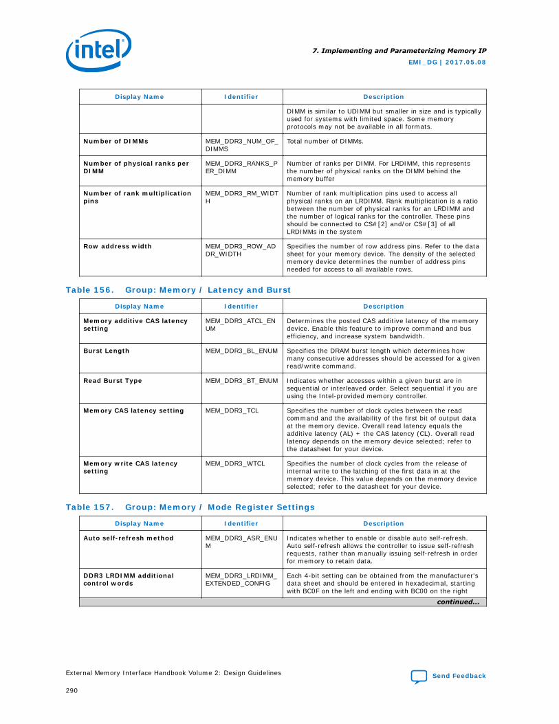
Display Name Identifier Description
DIMM is similar to UDIMM but smaller in size and is typicallyused for systems with limited space. Some memoryprotocols may not be available in all formats.
Number of DIMMs MEM_DDR3_NUM_OF_DIMMS
Total number of DIMMs.
Number of physical ranks perDIMM
MEM_DDR3_RANKS_PER_DIMM
Number of ranks per DIMM. For LRDIMM, this representsthe number of physical ranks on the DIMM behind thememory buffer
Number of rank multiplicationpins
MEM_DDR3_RM_WIDTH
Number of rank multiplication pins used to access allphysical ranks on an LRDIMM. Rank multiplication is a ratiobetween the number of physical ranks for an LRDIMM andthe number of logical ranks for the controller. These pinsshould be connected to CS#[2] and/or CS#[3] of allLRDIMMs in the system
Row address width MEM_DDR3_ROW_ADDR_WIDTH
Specifies the number of row address pins. Refer to the datasheet for your memory device. The density of the selectedmemory device determines the number of address pinsneeded for access to all available rows.
Table 156. Group: Memory / Latency and Burst
Display Name Identifier Description
Memory additive CAS latencysetting
MEM_DDR3_ATCL_ENUM
Determines the posted CAS additive latency of the memorydevice. Enable this feature to improve command and busefficiency, and increase system bandwidth.
Burst Length MEM_DDR3_BL_ENUM Specifies the DRAM burst length which determines howmany consecutive addresses should be accessed for a givenread/write command.
Read Burst Type MEM_DDR3_BT_ENUM Indicates whether accesses within a given burst are insequential or interleaved order. Select sequential if you areusing the Intel-provided memory controller.
Memory CAS latency setting MEM_DDR3_TCL Specifies the number of clock cycles between the readcommand and the availability of the first bit of output dataat the memory device. Overall read latency equals theadditive latency (AL) + the CAS latency (CL). Overall readlatency depends on the memory device selected; refer tothe datasheet for your device.
Memory write CAS latencysetting
MEM_DDR3_WTCL Specifies the number of clock cycles from the release ofinternal write to the latching of the first data in at thememory device. This value depends on the memory deviceselected; refer to the datasheet for your device.
Table 157. Group: Memory / Mode Register Settings
Display Name Identifier Description
Auto self-refresh method MEM_DDR3_ASR_ENUM
Indicates whether to enable or disable auto self-refresh.Auto self-refresh allows the controller to issue self-refreshrequests, rather than manually issuing self-refresh in orderfor memory to retain data.
DDR3 LRDIMM additionalcontrol words
MEM_DDR3_LRDIMM_EXTENDED_CONFIG
Each 4-bit setting can be obtained from the manufacturer'sdata sheet and should be entered in hexadecimal, startingwith BC0F on the left and ending with BC00 on the right
continued...
7. Implementing and Parameterizing Memory IP
EMI_DG | 2017.05.08
External Memory Interface Handbook Volume 2: Design Guidelines Send Feedback
290
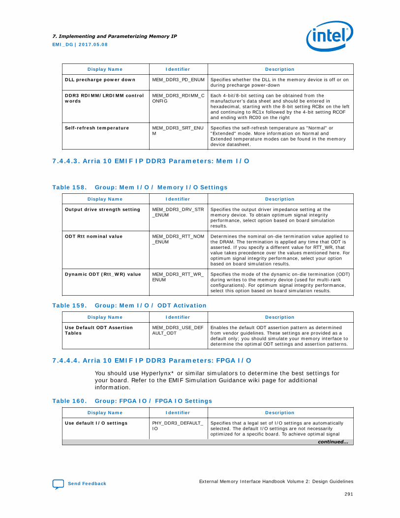
Display Name Identifier Description
DLL precharge power down MEM_DDR3_PD_ENUM Specifies whether the DLL in the memory device is off or onduring precharge power-down
DDR3 RDIMM/LRDIMM controlwords
MEM_DDR3_RDIMM_CONFIG
Each 4-bit/8-bit setting can be obtained from themanufacturer's data sheet and should be entered inhexadecimal, starting with the 8-bit setting RCBx on the leftand continuing to RC1x followed by the 4-bit setting RCOFand ending with RC00 on the right
Self-refresh temperature MEM_DDR3_SRT_ENUM
Specifies the self-refresh temperature as "Normal" or"Extended" mode. More information on Normal andExtended temperature modes can be found in the memorydevice datasheet.
7.4.4.3. Arria 10 EMIF IP DDR3 Parameters: Mem I/O
Table 158. Group: Mem I/O / Memory I/O Settings
Display Name Identifier Description
Output drive strength setting MEM_DDR3_DRV_STR_ENUM
Specifies the output driver impedance setting at thememory device. To obtain optimum signal integrityperformance, select option based on board simulationresults.
ODT Rtt nominal value MEM_DDR3_RTT_NOM_ENUM
Determines the nominal on-die termination value applied tothe DRAM. The termination is applied any time that ODT isasserted. If you specify a different value for RTT_WR, thatvalue takes precedence over the values mentioned here. Foroptimum signal integrity performance, select your optionbased on board simulation results.
Dynamic ODT (Rtt_WR) value MEM_DDR3_RTT_WR_ENUM
Specifies the mode of the dynamic on-die termination (ODT)during writes to the memory device (used for multi-rankconfigurations). For optimum signal integrity performance,select this option based on board simulation results.
Table 159. Group: Mem I/O / ODT Activation
Display Name Identifier Description
Use Default ODT AssertionTables
MEM_DDR3_USE_DEFAULT_ODT
Enables the default ODT assertion pattern as determinedfrom vendor guidelines. These settings are provided as adefault only; you should simulate your memory interface todetermine the optimal ODT settings and assertion patterns.
7.4.4.4. Arria 10 EMIF IP DDR3 Parameters: FPGA I/O
You should use Hyperlynx* or similar simulators to determine the best settings foryour board. Refer to the EMIF Simulation Guidance wiki page for additionalinformation.
Table 160. Group: FPGA IO / FPGA IO Settings
Display Name Identifier Description
Use default I/O settings PHY_DDR3_DEFAULT_IO
Specifies that a legal set of I/O settings are automaticallyselected. The default I/O settings are not necessarilyoptimized for a specific board. To achieve optimal signal
continued...
7. Implementing and Parameterizing Memory IP
EMI_DG | 2017.05.08
Send Feedback External Memory Interface Handbook Volume 2: Design Guidelines
291

Display Name Identifier Description
integrity, perform I/O simulations with IBIS models andenter the I/O settings manually, based on simulationresults.
Voltage PHY_DDR3_IO_VOLTAGE
The voltage level for the I/O pins driving the signalsbetween the memory device and the FPGA memoryinterface.
Periodic OCT re-calibration PHY_USER_PERIODIC_OCT_RECAL_ENUM
Specifies that the system periodically recalibrate on-chiptermination (OCT) to minimize variations in terminationvalue caused by changing operating conditions (such aschanges in temperature). By recalibrating OCT, I/O timingmargins are improved. When enabled, this parametercauses the PHY to halt user traffic about every 0.5 secondsfor about 1900 memory clock cycles, to perform OCTrecalibration. Efficiency is reduced by about 1% when thisoption is enabled.
Table 161. Group: FPGA IO / Address/Command
Display Name Identifier Description
I/O standard PHY_DDR3_USER_AC_IO_STD_ENUM
Specifies the I/O electrical standard for the address/command pins of the memory interface. The selected I/Ostandard configures the circuit within the I/O buffer tomatch the industry standard.
Output mode PHY_DDR3_USER_AC_MODE_ENUM
This parameter allows you to change the current drivestrength or termination settings for the selected I/Ostandard. Perform board simulation with IBIS models todetermine the best settings for your design.
Slew rate PHY_DDR3_USER_AC_SLEW_RATE_ENUM
Specifies the slew rate of the address/command outputpins. The slew rate (or edge rate) describes how quickly thesignal can transition, measured in voltage per unit time.Perform board simulations to determine the slew rate thatprovides the best eye opening for the address andcommand signals.
Table 162. Group: FPGA IO / Memory Clock
Display Name Identifier Description
I/O standard PHY_DDR3_USER_CK_IO_STD_ENUM
Specifies the I/O electrical standard for the memory clockpins. The selected I/O standard configures the circuit withinthe I/O buffer to match the industry standard.
Output mode PHY_DDR3_USER_CK_MODE_ENUM
This parameter allows you to change the current drivestrength or termination settings for the selected I/Ostandard. Perform board simulation with IBIS models todetermine the best settings for your design.
Slew rate PHY_DDR3_USER_CK_SLEW_RATE_ENUM
Specifies the slew rate of the address/command outputpins. The slew rate (or edge rate) describes how quickly thesignal can transition, measured in voltage per unit time.Perform board simulations to determine the slew rate thatprovides the best eye opening for the address andcommand signals.
7. Implementing and Parameterizing Memory IP
EMI_DG | 2017.05.08
External Memory Interface Handbook Volume 2: Design Guidelines Send Feedback
292

Table 163. Group: FPGA IO / Data Bus
Display Name Identifier Description
Use recommended initial Vrefin PHY_DDR3_USER_AUTO_STARTING_VREFIN_EN
Specifies that the initial Vrefin setting is calculatedautomatically, to a reasonable value based on terminationsettings.
Input mode PHY_DDR3_USER_DATA_IN_MODE_ENUM
This parameter allows you to change the input terminationsettings for the selected I/O standard. Perform boardsimulation with IBIS models to determine the best settingsfor your design.
I/O standard PHY_DDR3_USER_DATA_IO_STD_ENUM
Specifies the I/O electrical standard for the data and dataclock/strobe pins of the memory interface. The selected I/Ostandard option configures the circuit within the I/O bufferto match the industry standard.
Output mode PHY_DDR3_USER_DATA_OUT_MODE_ENUM
This parameter allows you to change the output currentdrive strength or termination settings for the selected I/Ostandard. Perform board simulation with IBIS models todetermine the best settings for your design.
Initial Vrefin PHY_DDR3_USER_STARTING_VREFIN
Specifies the initial value for the reference voltage on thedata pins (Vrefin). This value is entered as a percentage ofthe supply voltage level on the I/O pins. The specified valueserves as a starting point and may be overridden bycalibration to provide better timing margins. If you chooseto skip Vref calibration (Diagnostics tab), this is the valuethat is used as the Vref for the interface.
Table 164. Group: FPGA IO / PHY Inputs
Display Name Identifier Description
PLL reference clock I/Ostandard
PHY_DDR3_USER_PLL_REF_CLK_IO_STD_ENUM
Specifies the I/O standard for the PLL reference clock of thememory interface.
RZQ I/O standard PHY_DDR3_USER_RZQ_IO_STD_ENUM
Specifies the I/O standard for the RZQ pin used in thememory interface.
RZQ resistor PHY_RZQ Specifies the reference resistor used to calibrate the on-chiptermination value. You should connect the RZQ pin to GNDthrough an external resistor of the specified value.
7.4.4.5. Arria 10 EMIF IP DDR3 Parameters: Mem Timing
These parameters should be read from the table in the datasheet associated with thespeed bin of the memory device (not necessarily the frequency at which the interfaceis running).
Table 165. Group: Mem Timing / Parameters dependent on Speed Bin
Display Name Identifier Description
Speed bin MEM_DDR3_SPEEDBIN_ENUM
The speed grade of the memory device used. Thisparameter refers to the maximum rate at which thememory device is specified to run.
tDH (base) DC level MEM_DDR3_TDH_DC_MV
tDH (base) DC level refers to the voltage level which thedata bus must not cross during the hold window. The signalis considered stable only if it remains above this voltagelevel (for a logic 1) or below this voltage level (for a logic 0)for the entire hold period.
tDH (base) MEM_DDR3_TDH_PS tDH (base) refers to the hold time for the Data (DQ) busafter the rising edge of CK.
continued...
7. Implementing and Parameterizing Memory IP
EMI_DG | 2017.05.08
Send Feedback External Memory Interface Handbook Volume 2: Design Guidelines
293
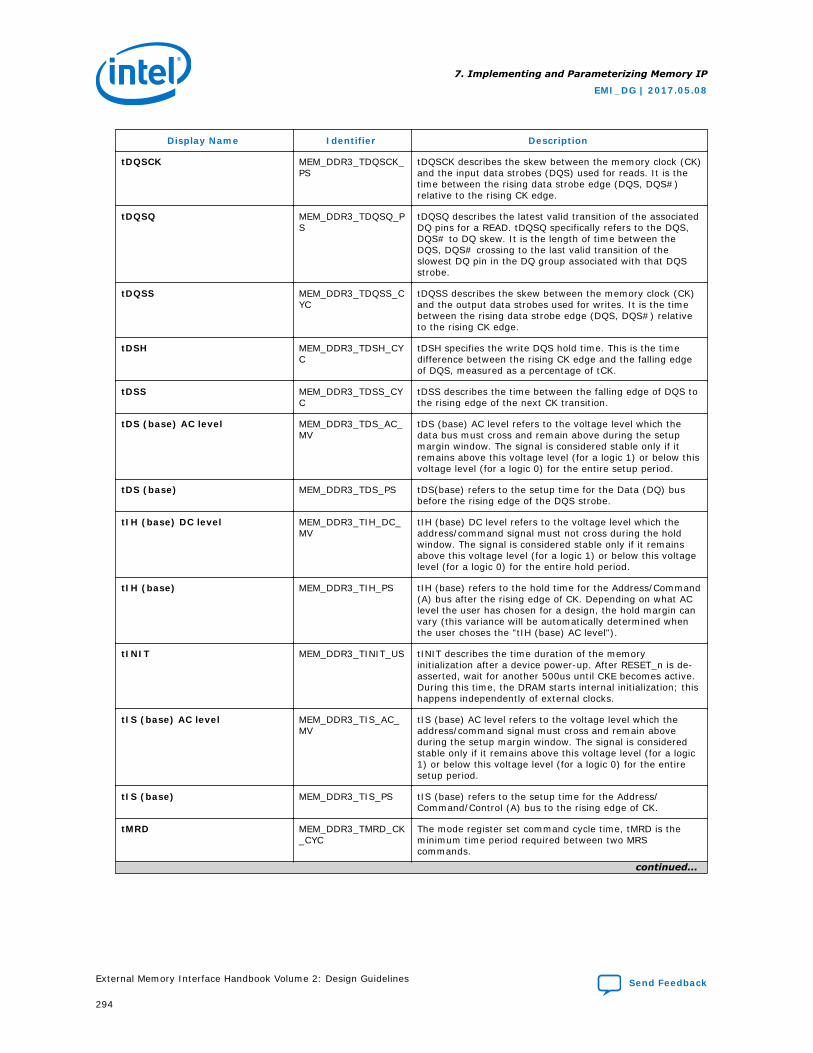
Display Name Identifier Description
tDQSCK MEM_DDR3_TDQSCK_PS
tDQSCK describes the skew between the memory clock (CK)and the input data strobes (DQS) used for reads. It is thetime between the rising data strobe edge (DQS, DQS#)relative to the rising CK edge.
tDQSQ MEM_DDR3_TDQSQ_PS
tDQSQ describes the latest valid transition of the associatedDQ pins for a READ. tDQSQ specifically refers to the DQS,DQS# to DQ skew. It is the length of time between theDQS, DQS# crossing to the last valid transition of theslowest DQ pin in the DQ group associated with that DQSstrobe.
tDQSS MEM_DDR3_TDQSS_CYC
tDQSS describes the skew between the memory clock (CK)and the output data strobes used for writes. It is the timebetween the rising data strobe edge (DQS, DQS#) relativeto the rising CK edge.
tDSH MEM_DDR3_TDSH_CYC
tDSH specifies the write DQS hold time. This is the timedifference between the rising CK edge and the falling edgeof DQS, measured as a percentage of tCK.
tDSS MEM_DDR3_TDSS_CYC
tDSS describes the time between the falling edge of DQS tothe rising edge of the next CK transition.
tDS (base) AC level MEM_DDR3_TDS_AC_MV
tDS (base) AC level refers to the voltage level which thedata bus must cross and remain above during the setupmargin window. The signal is considered stable only if itremains above this voltage level (for a logic 1) or below thisvoltage level (for a logic 0) for the entire setup period.
tDS (base) MEM_DDR3_TDS_PS tDS(base) refers to the setup time for the Data (DQ) busbefore the rising edge of the DQS strobe.
tIH (base) DC level MEM_DDR3_TIH_DC_MV
tIH (base) DC level refers to the voltage level which theaddress/command signal must not cross during the holdwindow. The signal is considered stable only if it remainsabove this voltage level (for a logic 1) or below this voltagelevel (for a logic 0) for the entire hold period.
tIH (base) MEM_DDR3_TIH_PS tIH (base) refers to the hold time for the Address/Command(A) bus after the rising edge of CK. Depending on what AClevel the user has chosen for a design, the hold margin canvary (this variance will be automatically determined whenthe user choses the "tIH (base) AC level").
tINIT MEM_DDR3_TINIT_US tINIT describes the time duration of the memoryinitialization after a device power-up. After RESET_n is de-asserted, wait for another 500us until CKE becomes active.During this time, the DRAM starts internal initialization; thishappens independently of external clocks.
tIS (base) AC level MEM_DDR3_TIS_AC_MV
tIS (base) AC level refers to the voltage level which theaddress/command signal must cross and remain aboveduring the setup margin window. The signal is consideredstable only if it remains above this voltage level (for a logic1) or below this voltage level (for a logic 0) for the entiresetup period.
tIS (base) MEM_DDR3_TIS_PS tIS (base) refers to the setup time for the Address/Command/Control (A) bus to the rising edge of CK.
tMRD MEM_DDR3_TMRD_CK_CYC
The mode register set command cycle time, tMRD is theminimum time period required between two MRScommands.
continued...
7. Implementing and Parameterizing Memory IP
EMI_DG | 2017.05.08
External Memory Interface Handbook Volume 2: Design Guidelines Send Feedback
294

Display Name Identifier Description
tQH MEM_DDR3_TQH_CYC tQH specifies the output hold time for the DQ in relation toDQS, DQS#. It is the length of time between the DQS,DQS# crossing to the earliest invalid transition of thefastest DQ pin in the DQ group associated with that DQSstrobe.
tQSH MEM_DDR3_TQSH_CYC
tQSH refers to the differential High Pulse Width, which ismeasured as a percentage of tCK. It is the time duringwhich the DQS is high for a read.
tRAS MEM_DDR3_TRAS_NS tRAS describes the activate to precharge duration. A rowcannot be deactivated until the tRAS time has been met.Therefore tRAS determines how long the memory has towait after a activate command before a precharge commandcan be issued to close the row.
tRCD MEM_DDR3_TRCD_NS tRCD, row command delay, describes the amount of delaybetween the activation of a row through the RAS commandand the access to the data through the CAS command.
tRP MEM_DDR3_TRP_NS tRP refers to the Precharge (PRE) command period. Itdescribes how long it takes for the memory to disableaccess to a row by precharging and before it is ready toactivate a different row.
tWLH MEM_DDR3_TWLH_PS tWLH describes the write leveling hold time from the risingedge of DQS to the rising edge of CK.
tWLS MEM_DDR3_TWLS_PS tWLS describes the write leveling setup time. It is measuredfrom the rising edge of CK to the rising edge of DQS.
tWR MEM_DDR3_TWR_NS tWR refers to the Write Recovery time. It specifies theamount of clock cycles needed to complete a write before aprecharge command can be issued.
Table 166. Group: Mem Timing / Parameters dependent on Speed Bin, OperatingFrequency, and Page Size
Display Name Identifier Description
tFAW MEM_DDR3_TFAW_NS tFAW refers to the four activate window time. It describesthe period of time during which only four banks can beactive.
tRRD MEM_DDR3_TRRD_CYC
tRRD refers to the Row Active to Row Active Delay. It is theminimum time interval (measured in memory clock cycles)between two activate commands to rows in different banksin the same rank
tRTP MEM_DDR3_TRTP_CYC
tRTP refers to the internal READ Command to PRECHARGECommand delay. It is the number of memory clock cyclesthat is needed between a read command and a prechargecommand to the same rank.
tWTR MEM_DDR3_TWTR_CYC
tWTR or Write Timing Parameter describes the delay fromstart of internal write transaction to internal read command,for accesses to the same bank. The delay is measured fromthe first rising memory clock edge after the last write datais received to the rising memory clock edge when a readcommand is received.
7. Implementing and Parameterizing Memory IP
EMI_DG | 2017.05.08
Send Feedback External Memory Interface Handbook Volume 2: Design Guidelines
295
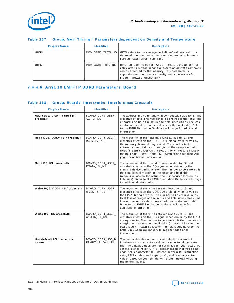
Table 167. Group: Mem Timing / Parameters dependent on Density and Temperature
Display Name Identifier Description
tREFI MEM_DDR3_TREFI_US tREFI refers to the average periodic refresh interval. It isthe maximum amount of time the memory can tolerate inbetween each refresh command
tRFC MEM_DDR3_TRFC_NS tRFC refers to the Refresh Cycle Time. It is the amount ofdelay after a refresh command before an activate commandcan be accepted by the memory. This parameter isdependent on the memory density and is necessary forproper hardware functionality.
7.4.4.6. Arria 10 EMIF IP DDR3 Parameters: Board
Table 168. Group: Board / Intersymbol Interference/Crosstalk
Display Name Identifier Description
Address and command ISI/crosstalk
BOARD_DDR3_USER_AC_ISI_NS
The address and command window reduction due to ISI andcrosstalk effects. The number to be entered is the total lossof margin on both the setup and hold sides (measured losson the setup side + measured loss on the hold side). Referto the EMIF Simulation Guidance wiki page for additionalinformation.
Read DQS/DQS# ISI/crosstalk BOARD_DDR3_USER_RCLK_ISI_NS
The reduction of the read data window due to ISI andcrosstalk effects on the DQS/DQS# signal when driven bythe memory device during a read. The number to beentered is the total loss of margin on the setup and holdsides (measured loss on the setup side + measured loss onthe hold side). Refer to the EMIF Simulation Guidance wikipage for additional information.
Read DQ ISI/crosstalk BOARD_DDR3_USER_RDATA_ISI_NS
The reduction of the read data window due to ISI andcrosstalk effects on the DQ signal when driven by thememory device during a read. The number to be entered isthe total loss of margin on the setup and hold side(measured loss on the setup side + measured loss on thehold side). Refer to the EMIF Simulation Guidance wiki pagefor additional information.
Write DQS/DQS# ISI/crosstalk BOARD_DDR3_USER_WCLK_ISI_NS
The reduction of the write data window due to ISI andcrosstalk effects on the DQS/DQS# signal when driven bythe FPGA during a write. The number to be entered is thetotal loss of margin on the setup and hold sides (measuredloss on the setup side + measured loss on the hold side).Refer to the EMIF Simulation Guidance wiki page foradditional information.
Write DQ ISI/crosstalk BOARD_DDR3_USER_WDATA_ISI_NS
The reduction of the write data window due to ISI andcrosstalk effects on the DQ signal when driven by the FPGAduring a write. The number to be entered is the total loss ofmargin on the setup and hold sides (measured loss on thesetup side + measured loss on the hold side). Refer to theEMIF Simulation Guidance wiki page for additionalinformation.
Use default ISI/crosstalkvalues
BOARD_DDR3_USE_DEFAULT_ISI_VALUES
You can enable this option to use default intersymbolinterference and crosstalk values for your topology. Notethat the default values are not optimized for your board. Foroptimal signal integrity, it is recommended that you do notenable this parameter, but instead perform I/O simulationusing IBIS models and Hyperlynx*, and manually entervalues based on your simulation results, instead of usingthe default values.
7. Implementing and Parameterizing Memory IP
EMI_DG | 2017.05.08
External Memory Interface Handbook Volume 2: Design Guidelines Send Feedback
296
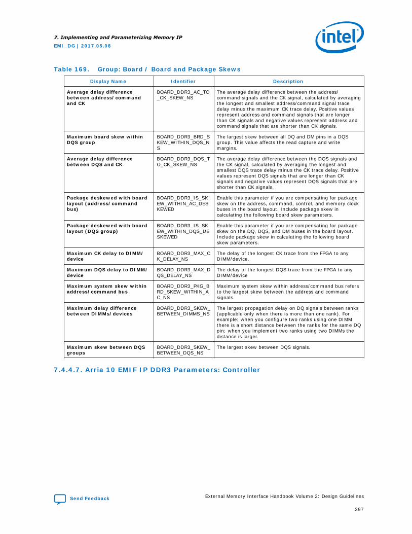
Table 169. Group: Board / Board and Package Skews
Display Name Identifier Description
Average delay differencebetween address/commandand CK
BOARD_DDR3_AC_TO_CK_SKEW_NS
The average delay difference between the address/command signals and the CK signal, calculated by averagingthe longest and smallest address/command signal tracedelay minus the maximum CK trace delay. Positive valuesrepresent address and command signals that are longerthan CK signals and negative values represent address andcommand signals that are shorter than CK signals.
Maximum board skew withinDQS group
BOARD_DDR3_BRD_SKEW_WITHIN_DQS_NS
The largest skew between all DQ and DM pins in a DQSgroup. This value affects the read capture and writemargins.
Average delay differencebetween DQS and CK
BOARD_DDR3_DQS_TO_CK_SKEW_NS
The average delay difference between the DQS signals andthe CK signal, calculated by averaging the longest andsmallest DQS trace delay minus the CK trace delay. Positivevalues represent DQS signals that are longer than CKsignals and negative values represent DQS signals that areshorter than CK signals.
Package deskewed with boardlayout (address/commandbus)
BOARD_DDR3_IS_SKEW_WITHIN_AC_DESKEWED
Enable this parameter if you are compensating for packageskew on the address, command, control, and memory clockbuses in the board layout. Include package skew incalculating the following board skew parameters.
Package deskewed with boardlayout (DQS group)
BOARD_DDR3_IS_SKEW_WITHIN_DQS_DESKEWED
Enable this parameter if you are compensating for packageskew on the DQ, DQS, and DM buses in the board layout.Include package skew in calculating the following boardskew parameters.
Maximum CK delay to DIMM/device
BOARD_DDR3_MAX_CK_DELAY_NS
The delay of the longest CK trace from the FPGA to anyDIMM/device.
Maximum DQS delay to DIMM/device
BOARD_DDR3_MAX_DQS_DELAY_NS
The delay of the longest DQS trace from the FPGA to anyDIMM/device
Maximum system skew withinaddress/command bus
BOARD_DDR3_PKG_BRD_SKEW_WITHIN_AC_NS
Maximum system skew within address/command bus refersto the largest skew between the address and commandsignals.
Maximum delay differencebetween DIMMs/devices
BOARD_DDR3_SKEW_BETWEEN_DIMMS_NS
The largest propagation delay on DQ signals between ranks(applicable only when there is more than one rank). Forexample: when you configure two ranks using one DIMMthere is a short distance between the ranks for the same DQpin; when you implement two ranks using two DIMMs thedistance is larger.
Maximum skew between DQSgroups
BOARD_DDR3_SKEW_BETWEEN_DQS_NS
The largest skew between DQS signals.
7.4.4.7. Arria 10 EMIF IP DDR3 Parameters: Controller
7. Implementing and Parameterizing Memory IP
EMI_DG | 2017.05.08
Send Feedback External Memory Interface Handbook Volume 2: Design Guidelines
297

Table 170. Group: Controller / Low Power Mode
Display Name Identifier Description
Auto Power-Down Cycles CTRL_DDR3_AUTO_POWER_DOWN_CYCS
Specifies the number of idle controller cycles after which thememory device is placed into power-down mode. You canconfigure the idle waiting time. The supported range fornumber of cycles is from 1 to 65534.
Enable Auto Power-Down CTRL_DDR3_AUTO_POWER_DOWN_EN
Enable this parameter to have the controller automaticallyplace the memory device into power-down mode after aspecified number of idle controller clock cycles. The idle waittime is configurable. All ranks must be idle to enter autopower-down.
Table 171. Group: Controller / Efficiency
Display Name Identifier Description
Address Ordering CTRL_DDR3_ADDR_ORDER_ENUM
Controls the mapping between Avalon addresses andmemory device addresses. By changing the value of thisparameter, you can change the mappings between theAvalon-MM address and the DRAM address.
Enable Auto-Precharge Control CTRL_DDR3_AUTO_PRECHARGE_EN
Select this parameter to enable the auto-precharge controlon the controller top level. If you assert the auto-prechargecontrol signal while requesting a read or write burst, youcan specify whether the controller should close (auto-precharge) the currently open page at the end of the reador write burst, potentially making a future access to adifferent page of the same bank faster.
Enable Reordering CTRL_DDR3_REORDER_EN
Enable this parameter to allow the controller to performcommand and data reordering. Reordering can improveefficiency by reducing bus turnaround time and row/bankswitching time. Data reordering allows the single-portmemory controller to change the order of read and writecommands to achieve highest efficiency. Commandreordering allows the controller to issue bank managementcommands early based on incoming patterns, so that thedesired row in memory is already open when the commandreaches the memory interface. For more information, referto the Data Reordering topic in the EMIF Handbook.
Starvation limit for eachcommand
CTRL_DDR3_STARVE_LIMIT
Specifies the number of commands that can be servedbefore a waiting command is served. The controller employsa counter to ensure that all requests are served after a pre-defined interval -- this ensures that low priority requests arenot ignored, when doing data reordering for efficiency. Thevalid range for this parameter is from 1 to 63. For moreinformation, refer to the Starvation Control topic in the EMIFHandbook.
Enable Command PriorityControl
CTRL_DDR3_USER_PRIORITY_EN
Select this parameter to enable user-requested commandpriority control on the controller top level. This parameterinstructs the controller to treat a read or write request ashigh-priority. The controller attempts to fill high-priorityrequests sooner, to reduce latency. Connect this interface tothe conduit of your logic block that determines when theexternal memory interface IP treats the read or writerequest as a high-priority command.
7. Implementing and Parameterizing Memory IP
EMI_DG | 2017.05.08
External Memory Interface Handbook Volume 2: Design Guidelines Send Feedback
298

Table 172. Group: Controller / Configuration, Status, and Error Handling
Display Name Identifier Description
Enable Auto Error Correction CTRL_DDR3_ECC_AUTO_CORRECTION_EN
Specifies that the controller perform auto correction when asingle-bit error is detected by the ECC logic.
Enable Error Detection andCorrection Logic with ECC
CTRL_DDR3_ECC_EN Enables error-correction code (ECC) for single-bit errorcorrection and double-bit error detection. Your memoryinterface must have a width of 16, 24, 40, or 72 bits to useECC. ECC is implemented as soft logic.
Enable Memory-MappedConfiguration and StatusRegister (MMR) Interface
CTRL_DDR3_MMR_EN Enable this parameter to change or read memory timingparameters, memory address size, mode register settings,controller status, and request sideband operations.
Table 173. Group: Controller / Data Bus Turnaround Time
Display Name Identifier Description
Additional read-to-readturnaround time (differentranks)
CTRL_DDR3_RD_TO_RD_DIFF_CHIP_DELTA_CYCS
Specifies additional number of idle controller (not DRAM)cycles when switching the data bus from a read of onelogical rank to a read of another logical rank. This canresolve bus contention problems specific to your boardtopology. The value is added to the default which iscalculated automatically. Use the default setting unless yoususpect a problem exists.
Additional read-to-writeturnaround time (differentranks)
CTRL_DDR3_RD_TO_WR_DIFF_CHIP_DELTA_CYCS
Specifies additional number of idle controller (not DRAM)cycles when switching the data bus from a read of onelogical rank to a write of another logical rank. This can helpresolve bus contention problems specific to your boardtopology. The value is added to the default which iscalculated automatically. Use the default setting unless yoususpect a problem exists.
Additional read-to-writeturnaround time (same rank)
CTRL_DDR3_RD_TO_WR_SAME_CHIP_DELTA_CYCS
Specifies additional number of idle controller (not DRAM)cycles when switching the data bus from a read to a writewithin the same logical rank. This can help resolve buscontention problems specific to your board topology. Thevalue is added to the default which is calculatedautomatically. Use the default setting unless you suspect aproblem exists.
Additional write-to-readturnaround time (differentranks)
CTRL_DDR3_WR_TO_RD_DIFF_CHIP_DELTA_CYCS
Specifies additional number of idle controller (not DRAM)cycles when switching the data bus from a write of onelogical rank to a read of another logical rank. This can helpresolve bus contention problems specific to your boardtopology. The value is added to the default which iscalculated automatically. Use the default setting unless yoususpect a problem exists.
Additional write-to-readturnaround time (same rank)
CTRL_DDR3_WR_TO_RD_SAME_CHIP_DELTA_CYCS
Specifies additional number of idle controller (not DRAM)cycles when switching the data bus from a write to a readwithin the same logical rank. This can help resolve buscontention problems specific to your board topology. Thevalue is added to the default which is calculatedautomatically. Use the default setting unless you suspect aproblem exists.
Additional write-to-writeturnaround time (differentranks)
CTRL_DDR3_WR_TO_WR_DIFF_CHIP_DELTA_CYCS
Specifies additional number of idle controller (not DRAM)cycles when switching the data bus from a write of onelogical rank to a write of another logical rank. This can helpresolve bus contention problems specific to your boardtopology. The value is added to the default which iscalculated automatically. Use the default setting unless yoususpect a problem exists.
7. Implementing and Parameterizing Memory IP
EMI_DG | 2017.05.08
Send Feedback External Memory Interface Handbook Volume 2: Design Guidelines
299

7.4.4.8. Arria 10 EMIF IP DDR3 Parameters: Diagnostics
Table 174. Group: Diagnostics / Simulation Options
Display Name Identifier Description
Abstract phy for fast simulation DIAG_DDR3_ABSTRACT_PHY
Specifies that the system use Abstract PHY for simulation.Abstract PHY replaces the PHY with a model for fastsimulation and can reduce simulation time by 2-3 times.Abstract PHY is available for certain protocols and devicefamilies, and only when you select Skip Calibration.
Calibration mode DIAG_SIM_CAL_MODE_ENUM
Specifies whether to skip memory interface calibrationduring simulation, or to simulate the full calibration process.Simulating the full calibration process can take hours (oreven days), depending on the width and depth of thememory interface. You can achieve much faster simulationtimes by skipping the calibration process, but that is onlyexpected to work when the memory model is ideal and theinterconnect delays are zero. If you enable this parameter,the interface still performs some memory initializationbefore starting normal operations. Abstract PHY issupported with skip calibration.
Table 175. Group: Diagnostics / Calibration Debug Options
Display Name Identifier Description
Enable Daisy-Chaining forQuartus Prime EMIF DebugToolkit/On-Chip Debug Port
DIAG_EXPORT_SEQ_AVALON_MASTER
Specifies that the IP export an Avalon-MM master interface(cal_debug_out) which can connect to the cal_debuginterface of other EMIF cores residing in the same I/Ocolumn. This parameter applies only if the EMIF DebugToolkit or On-Chip Debug Port is enabled. Refer to theDebugging Multiple EMIFs wiki page for more informationabout debugging multiple EMIFs.
Quartus Prime EMIF DebugToolkit/On-Chip Debug Port
DIAG_EXPORT_SEQ_AVALON_SLAVE
Specifies the connectivity of an Avalon slave interface foruse by the Quartus Prime EMIF Debug Toolkit or user corelogic. If you set this parameter to "Disabled," no debugfeatures are enabled. If you set this parameter to "Export,"an Avalon slave interface named "cal_debug" is exportedfrom the IP. To use this interface with the EMIF DebugToolkit, you must instantiate and connect an EMIF debuginterface IP core to it, or connect it to the cal_debug_outinterface of another EMIF core. If you select "Add EMIFDebug Interface", an EMIF debug interface componentcontaining a JTAG Avalon Master is connected to the debugport, allowing the core to be accessed by the EMIF DebugToolkit. Only one EMIF debug interface should beinstantiated per I/O column. You can chain additional EMIFor PHYLite cores to the first by enabling the "Enable Daisy-Chaining for Quartus Prime EMIF Debug Toolkit/On-ChipDebug Port" option for all cores in the chain, and selecting"Export" for the "Quartus Prime EMIF Debug Toolkit/On-ChipDebug Port" option on all cores after the first.
Interface ID DIAG_INTERFACE_ID Identifies interfaces within the I/O column, for use by theEMIF Debug Toolkit and the On-Chip Debug Port. InterfaceIDs should be unique among EMIF cores within the sameI/O column. If the Quartus Prime EMIF Debug Toolkit/On-Chip Debug Port parameter is set to Disabled, the interfaceID is unused.
Use Soft NIOS Processor forOn-Chip Debug
DIAG_SOFT_NIOS_MODE
Enables a soft Nios processor as a peripheral component toaccess the On-Chip Debug Port. Only one interface in acolumn can activate this option.
7. Implementing and Parameterizing Memory IP
EMI_DG | 2017.05.08
External Memory Interface Handbook Volume 2: Design Guidelines Send Feedback
300

Table 176. Group: Diagnostics / Example Design
Display Name Identifier Description
Enable In-System-Sources-and-Probes
DIAG_EX_DESIGN_ISSP_EN
Enables In-System-Sources-and-Probes in the exampledesign for common debug signals, such as calibration statusor example traffic generator per-bit status. This parametermust be enabled if you want to do driver margining.
Number of core clocks sharingslaves to instantiate in theexample design
DIAG_EX_DESIGN_NUM_OF_SLAVES
Specifies the number of core clock sharing slaves toinstantiate in the example design. This parameter appliesonly if you set the "Core clocks sharing" parameter in the"General" tab to Master or Slave.
Table 177. Group: Diagnostics / Traffic Generator
Display Name Identifier Description
Bypass the default trafficpattern
DIAG_BYPASS_DEFAULT_PATTERN
Specifies that the controller/interface bypass the trafficgenerator 2.0 default pattern after reset. If you do notenable this parameter, the traffic generator does not asserta pass or fail status until the generator is configured andsignaled to start by its Avalon configuration interface.
Bypass the traffic generatorrepeated-writes/repeated-reads test pattern
DIAG_BYPASS_REPEAT_STAGE
Specifies that the controller/interface bypass the trafficgenerator's repeat test stage. If you do not enable thisparameter, every write and read is repeated several times.
Bypass the traffic generatorstress pattern
DIAG_BYPASS_STRESS_STAGE
Specifies that the controller/interface bypass the trafficgenerator's stress pattern stage. (Stress patterns are meantto create worst-case signal integrity patterns on the datapins.) If you do not enable this parameter, the trafficgenerator does not assert a pass or fail status until thegenerator is configured and signaled to start by its Avalonconfiguration interface.
Bypass the user-configuredtraffic stage
DIAG_BYPASS_USER_STAGE
Specifies that the controller/interface bypass the user-configured traffic generator's pattern after reset. If you donot enable this parameter, the traffic generator does notassert a pass or fail status until the generator is configuredand signaled to start by its Avalon configuration interface.Configuration can be done by connecting to the trafficgenerator via the EMIF Debug Toolkit, or by using customlogic connected to the Avalon-MM configuration slave porton the traffic generator. Configuration can also be simulatedusing the example testbench provided in thealtera_emif_avl_tg_2_tb.sv file.
Run diagnostic on infinite testduration
DIAG_INFI_TG2_ERR_TEST
Specifies that the traffic generator run indefinitely until thefirst error is detected.
Export Traffic Generator 2.0configuration interface
DIAG_TG_AVL_2_EXPORT_CFG_INTERFACE
Specifies that the IP export an Avalon-MM slave port forconfiguring the Traffic Generator. This is required only if youare configuring the traffic generator through user logic andnot through through the EMIF Debug Toolkit.
Use configurable Avalon trafficgenerator 2.0
DIAG_USE_TG_AVL_2 This option allows users to add the new configurable Avalontraffic generator to the example design.
Table 178. Group: Diagnostics / Performance
Display Name Identifier Description
Enable Efficiency Monitor DIAG_EFFICIENCY_MONITOR
Adds an Efficiency Monitor component to the Avalon-MMinterface of the memory controller, allowing you to viewefficiency statistics of the interface. You can access theefficiency statistics using the EMIF Debug Toolkit.
7. Implementing and Parameterizing Memory IP
EMI_DG | 2017.05.08
Send Feedback External Memory Interface Handbook Volume 2: Design Guidelines
301

Table 179. Group: Diagnostics / Miscellaneous
Display Name Identifier Description
Use short Qsys interface names SHORT_QSYS_INTERFACE_NAMES
Specifies the use of short interface names, for improvedusability and consistency with other Qsys components. Ifthis parameter is disabled, the names of Qsys interfacesexposed by the IP will include the type and direction of theinterface. Long interface names are supported forbackward-compatibility and will be removed in a futurerelease.
7.4.4.9. Arria 10 EMIF IP DDR3 Parameters: Example Designs
Table 180. Group: Example Designs / Available Example Designs
Display Name Identifier Description
Select design EX_DESIGN_GUI_DDR3_SEL_DESIGN
Specifies the creation of a full Quartus Prime project,instantiating an external memory interface and an exampletraffic generator, according to your parameterization. Afterthe design is created, you can specify the target device andpin location assignments, run a full compilation, verifytiming closure, and test the interface on your board usingthe programming file created by the Quartus Primeassembler. The 'Generate Example Design' button lets yougenerate simulation or synthesis file sets.
Table 181. Group: Example Designs / Example Design Files
Display Name Identifier Description
Simulation EX_DESIGN_GUI_DDR3_GEN_SIM
Specifies that the 'Generate Example Design' button createall necessary file sets for simulation. Expect a shortadditional delay as the file set is created. If you do notenable this parameter, simulation file sets are not created.Instead, the output directory will contain the ed_sim.qsysfile which holds Qsys details of the simulation exampledesign, and a make_sim_design.tcl file with othercorresponding tcl files. You can run make_sim_design.tclfrom a command line to generate the simulation exampledesign. The generated example designs for varioussimulators are stored in the /sim sub-directory.
Synthesis EX_DESIGN_GUI_DDR3_GEN_SYNTH
Specifies that the 'Generate Example Design' button createall necessary file sets for synthesis. Expect a shortadditional delay as the file set is created. If you do notenable this parameter, synthesis file sets are not created.Instead, the output directory will contain the ed_synth.qsysfile which holds Qsys details of the synthesis exampledesign, and a make_qii_design.tcl script with othercorresponding tcl files. You can run make_qii_design.tclfrom a command line to generate the synthesis exampledesign. The generated example design is stored in the /qiisub-directory.
Table 182. Group: Example Designs / Generated HDL Format
Display Name Identifier Description
Simulation HDL format EX_DESIGN_GUI_DDR3_HDL_FORMAT
This option lets you choose the format of HDL in whichgenerated simulation files are created.
7. Implementing and Parameterizing Memory IP
EMI_DG | 2017.05.08
External Memory Interface Handbook Volume 2: Design Guidelines Send Feedback
302
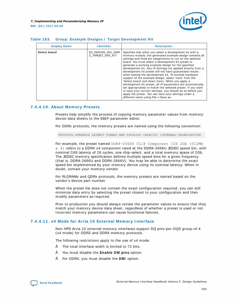
Table 183. Group: Example Designs / Target Development Kit
Display Name Identifier Description
Select board EX_DESIGN_GUI_DDR3_TARGET_DEV_KIT
Specifies that when you select a development kit with amemory module, the generated example design contains allsettings and fixed pin assignments to run on the selectedboard. You must select a development kit preset togenerate a working example design for the specifieddevelopment kit. Any IP settings not applied directly from adevelopment kit preset will not have guaranteed resultswhen testing the development kit. To exclude hardwaresupport of the example design, select 'none' from the'Select board' pull down menu. When you apply adevelopment kit preset, all IP parameters are automaticallyset appropriately to match the selected preset. If you wantto save your current settings, you should do so before youapply the preset. You can save your settings under adifferent name using File->Save as.
7.4.4.10. About Memory Presets
Presets help simplify the process of copying memory parameter values from memorydevice data sheets to the EMIF parameter editor.
For DDRx protocols, the memory presets are named using the following convention:
PROTOCOL-SPEEDBIN LATENCY FORMAT-AND-TOPOLOGY CAPACITY (INTERNAL-ORGANIZATION)
For example, the preset named DDR4-2666U CL18 Component 1CS 2Gb (512Mbx 4) refers to a DDR4 x4 component rated at the DDR4-2666U JEDEC speed bin, withnominal CAS latency of 18 cycles, one chip-select, and a total memory space of 2Gb.The JEDEC memory specification defines multiple speed bins for a given frequency(that is, DDR4-2666U and DDR4-2666V). You may be able to determine the exactspeed bin implemented by your memory device using its nominal latency. When indoubt, contact your memory vendor.
For RLDRAMx and QDRx protocols, the memory presets are named based on thevendor's device part number.
When the preset list does not contain the exact configuration required, you can stillminimize data entry by selecting the preset closest to your configuration and thenmodify parameters as required.
Prior to production you should always review the parameter values to ensure that theymatch your memory device data sheet, regardless of whether a preset is used or not.Incorrect memory parameters can cause functional failures.
7.4.4.11. x4 Mode for Arria 10 External Memory Interface
Non-HPS Arria 10 external memory interfaces support DQ pins-per-DQS group-of-4(x4 mode) for DDR3 and DDR4 memory protocols.
The following restrictions apply to the use of x4 mode:
• The total interface width is limited to 72 bits.
• You must disable the Enable DM pins option.
• For DDR4, you must disable the DBI option.
7. Implementing and Parameterizing Memory IP
EMI_DG | 2017.05.08
Send Feedback External Memory Interface Handbook Volume 2: Design Guidelines
303

Note: x4 mode is not available for Arria 10 EMIF IP for HPS.
7.4.4.12. Additional Notes About Parameterizing Arria 10 EMIF IP for HPS
Although Arria 10 EMIF IP and Arria 10 EMIF IP for HPS are similar components, thereare some additional requirements necessary in the HPS case.
The following rules and restrictions apply to Arria 10 EMIF IP for HPS:
• Supported memory protocols are limited to DDR3 and DDR4.
• The only supported configuration is the hard PHY with the hard memory controller.
• The maximum memory clock frequency for Arria 10 EMIF IP for HPS may bedifferent than for regular Arria 10 EMIF IP. Refer to the External Memory InterfaceSpec Estimator for details.
• Only half-rate interfaces are supported.
• Sharing of clocks is not supported.
• The total interface width is limited to a multiple of 16, 24, 40 or 72 bits (with ECCenabled), or a positive value divisible by the number of DQ pins per DQS group(with ECC not enabled). For devices other than 10ASXXXKX40, the total interfacewidth is further limited to a maximum of 40 bits with ECC enabled and 32 bits withECC not enabled.
• Only x8 data groups are supported; that is, DQ pins-per-DQS group must be 8.
• DM pins must be enabled.
• The EMIF debug toolkit is not supported.
• Ping Pong PHY is not supported.
7. Implementing and Parameterizing Memory IP
EMI_DG | 2017.05.08
External Memory Interface Handbook Volume 2: Design Guidelines Send Feedback
304
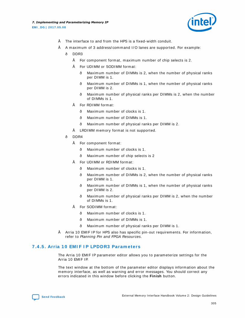
• The interface to and from the HPS is a fixed-width conduit.
• A maximum of 3 address/command I/O lanes are supported. For example:
— DDR3
• For component format, maximum number of chip selects is 2.
• For UDIMM or SODIMM format:
— Maximum number of DIMMs is 2, when the number of physical ranksper DIMM is 1.
— Maximum number of DIMMs is 1, when the number of physical ranksper DIMM is 2.
— Maximum number of physical ranks per DIMMs is 2, when the numberof DIMMs is 1.
• For RDIMM format:
— Maximum number of clocks is 1.
— Maximum number of DIMMs is 1.
— Maximum number of physical ranks per DIMM is 2.
• LRDIMM memory format is not supported.
— DDR4
• For component format:
— Maximum number of clocks is 1.
— Maximum number of chip selects is 2
• For UDIMM or RDIMM format:
— Maximum number of clocks is 1.
— Maximum number of DIMMs is 2, when the number of physical ranksper DIMM is 1.
— Maximum number of DIMMs is 1, when the number of physical ranksper DIMM is 2.
— Maximum number of physical ranks per DIMM is 2, when the numberof DIMMs is 1.
• For SODIMM format:
— Maximum number of clocks is 1.
— Maximum number of DIMMs is 1.
— Maximum number of physical ranks per DIMM is 1.
• Arria 10 EMIF IP for HPS also has specific pin-out requirements. For information,refer to Planning Pin and FPGA Resources.
7.4.5. Arria 10 EMIF IP LPDDR3 Parameters
The Arria 10 EMIF IP parameter editor allows you to parameterize settings for theArria 10 EMIF IP.
The text window at the bottom of the parameter editor displays information about thememory interface, as well as warning and error messages. You should correct anyerrors indicated in this window before clicking the Finish button.
7. Implementing and Parameterizing Memory IP
EMI_DG | 2017.05.08
Send Feedback External Memory Interface Handbook Volume 2: Design Guidelines
305
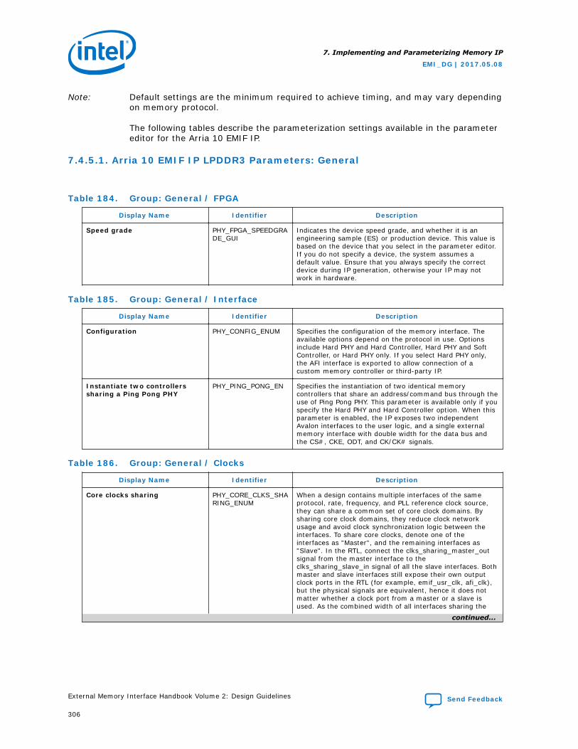
Note: Default settings are the minimum required to achieve timing, and may vary dependingon memory protocol.
The following tables describe the parameterization settings available in the parametereditor for the Arria 10 EMIF IP.
7.4.5.1. Arria 10 EMIF IP LPDDR3 Parameters: General
Table 184. Group: General / FPGA
Display Name Identifier Description
Speed grade PHY_FPGA_SPEEDGRADE_GUI
Indicates the device speed grade, and whether it is anengineering sample (ES) or production device. This value isbased on the device that you select in the parameter editor.If you do not specify a device, the system assumes adefault value. Ensure that you always specify the correctdevice during IP generation, otherwise your IP may notwork in hardware.
Table 185. Group: General / Interface
Display Name Identifier Description
Configuration PHY_CONFIG_ENUM Specifies the configuration of the memory interface. Theavailable options depend on the protocol in use. Optionsinclude Hard PHY and Hard Controller, Hard PHY and SoftController, or Hard PHY only. If you select Hard PHY only,the AFI interface is exported to allow connection of acustom memory controller or third-party IP.
Instantiate two controllerssharing a Ping Pong PHY
PHY_PING_PONG_EN Specifies the instantiation of two identical memorycontrollers that share an address/command bus through theuse of Ping Pong PHY. This parameter is available only if youspecify the Hard PHY and Hard Controller option. When thisparameter is enabled, the IP exposes two independentAvalon interfaces to the user logic, and a single externalmemory interface with double width for the data bus andthe CS#, CKE, ODT, and CK/CK# signals.
Table 186. Group: General / Clocks
Display Name Identifier Description
Core clocks sharing PHY_CORE_CLKS_SHARING_ENUM
When a design contains multiple interfaces of the sameprotocol, rate, frequency, and PLL reference clock source,they can share a common set of core clock domains. Bysharing core clock domains, they reduce clock networkusage and avoid clock synchronization logic between theinterfaces. To share core clocks, denote one of theinterfaces as "Master", and the remaining interfaces as"Slave". In the RTL, connect the clks_sharing_master_outsignal from the master interface to theclks_sharing_slave_in signal of all the slave interfaces. Bothmaster and slave interfaces still expose their own outputclock ports in the RTL (for example, emif_usr_clk, afi_clk),but the physical signals are equivalent, hence it does notmatter whether a clock port from a master or a slave isused. As the combined width of all interfaces sharing the
continued...
7. Implementing and Parameterizing Memory IP
EMI_DG | 2017.05.08
External Memory Interface Handbook Volume 2: Design Guidelines Send Feedback
306
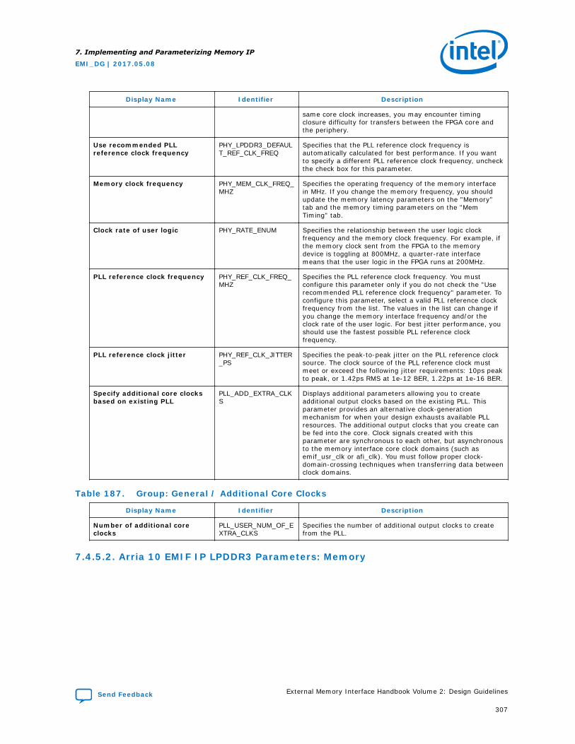
Display Name Identifier Description
same core clock increases, you may encounter timingclosure difficulty for transfers between the FPGA core andthe periphery.
Use recommended PLLreference clock frequency
PHY_LPDDR3_DEFAULT_REF_CLK_FREQ
Specifies that the PLL reference clock frequency isautomatically calculated for best performance. If you wantto specify a different PLL reference clock frequency, uncheckthe check box for this parameter.
Memory clock frequency PHY_MEM_CLK_FREQ_MHZ
Specifies the operating frequency of the memory interfacein MHz. If you change the memory frequency, you shouldupdate the memory latency parameters on the "Memory"tab and the memory timing parameters on the "MemTiming" tab.
Clock rate of user logic PHY_RATE_ENUM Specifies the relationship between the user logic clockfrequency and the memory clock frequency. For example, ifthe memory clock sent from the FPGA to the memorydevice is toggling at 800MHz, a quarter-rate interfacemeans that the user logic in the FPGA runs at 200MHz.
PLL reference clock frequency PHY_REF_CLK_FREQ_MHZ
Specifies the PLL reference clock frequency. You mustconfigure this parameter only if you do not check the "Userecommended PLL reference clock frequency" parameter. Toconfigure this parameter, select a valid PLL reference clockfrequency from the list. The values in the list can change ifyou change the memory interface frequency and/or theclock rate of the user logic. For best jitter performance, youshould use the fastest possible PLL reference clockfrequency.
PLL reference clock jitter PHY_REF_CLK_JITTER_PS
Specifies the peak-to-peak jitter on the PLL reference clocksource. The clock source of the PLL reference clock mustmeet or exceed the following jitter requirements: 10ps peakto peak, or 1.42ps RMS at 1e-12 BER, 1.22ps at 1e-16 BER.
Specify additional core clocksbased on existing PLL
PLL_ADD_EXTRA_CLKS
Displays additional parameters allowing you to createadditional output clocks based on the existing PLL. Thisparameter provides an alternative clock-generationmechanism for when your design exhausts available PLLresources. The additional output clocks that you create canbe fed into the core. Clock signals created with thisparameter are synchronous to each other, but asynchronousto the memory interface core clock domains (such asemif_usr_clk or afi_clk). You must follow proper clock-domain-crossing techniques when transferring data betweenclock domains.
Table 187. Group: General / Additional Core Clocks
Display Name Identifier Description
Number of additional coreclocks
PLL_USER_NUM_OF_EXTRA_CLKS
Specifies the number of additional output clocks to createfrom the PLL.
7.4.5.2. Arria 10 EMIF IP LPDDR3 Parameters: Memory
7. Implementing and Parameterizing Memory IP
EMI_DG | 2017.05.08
Send Feedback External Memory Interface Handbook Volume 2: Design Guidelines
307
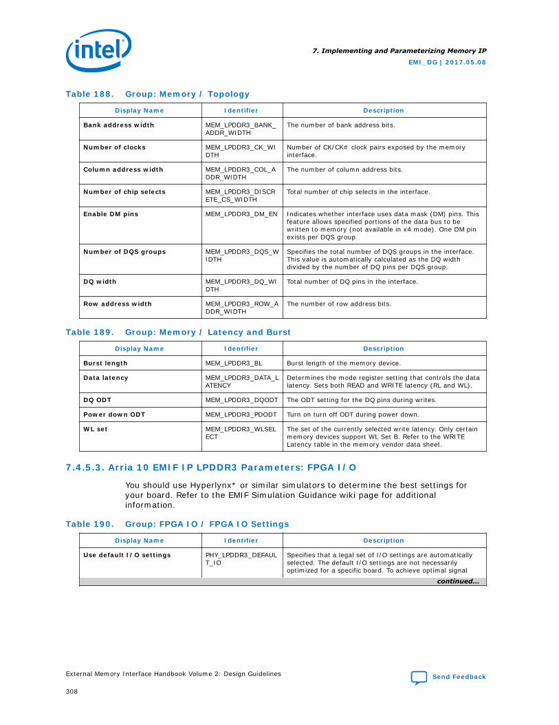
Table 188. Group: Memory / Topology
Display Name Identifier Description
Bank address width MEM_LPDDR3_BANK_ADDR_WIDTH
The number of bank address bits.
Number of clocks MEM_LPDDR3_CK_WIDTH
Number of CK/CK# clock pairs exposed by the memoryinterface.
Column address width MEM_LPDDR3_COL_ADDR_WIDTH
The number of column address bits.
Number of chip selects MEM_LPDDR3_DISCRETE_CS_WIDTH
Total number of chip selects in the interface.
Enable DM pins MEM_LPDDR3_DM_EN Indicates whether interface uses data mask (DM) pins. Thisfeature allows specified portions of the data bus to bewritten to memory (not available in x4 mode). One DM pinexists per DQS group
Number of DQS groups MEM_LPDDR3_DQS_WIDTH
Specifies the total number of DQS groups in the interface.This value is automatically calculated as the DQ widthdivided by the number of DQ pins per DQS group.
DQ width MEM_LPDDR3_DQ_WIDTH
Total number of DQ pins in the interface.
Row address width MEM_LPDDR3_ROW_ADDR_WIDTH
The number of row address bits.
Table 189. Group: Memory / Latency and Burst
Display Name Identifier Description
Burst length MEM_LPDDR3_BL Burst length of the memory device.
Data latency MEM_LPDDR3_DATA_LATENCY
Determines the mode register setting that controls the datalatency. Sets both READ and WRITE latency (RL and WL).
DQ ODT MEM_LPDDR3_DQODT The ODT setting for the DQ pins during writes.
Power down ODT MEM_LPDDR3_PDODT Turn on turn off ODT during power down.
WL set MEM_LPDDR3_WLSELECT
The set of the currently selected write latency. Only certainmemory devices support WL Set B. Refer to the WRITELatency table in the memory vendor data sheet.
7.4.5.3. Arria 10 EMIF IP LPDDR3 Parameters: FPGA I/O
You should use Hyperlynx* or similar simulators to determine the best settings foryour board. Refer to the EMIF Simulation Guidance wiki page for additionalinformation.
Table 190. Group: FPGA IO / FPGA IO Settings
Display Name Identifier Description
Use default I/O settings PHY_LPDDR3_DEFAULT_IO
Specifies that a legal set of I/O settings are automaticallyselected. The default I/O settings are not necessarilyoptimized for a specific board. To achieve optimal signal
continued...
7. Implementing and Parameterizing Memory IP
EMI_DG | 2017.05.08
External Memory Interface Handbook Volume 2: Design Guidelines Send Feedback
308
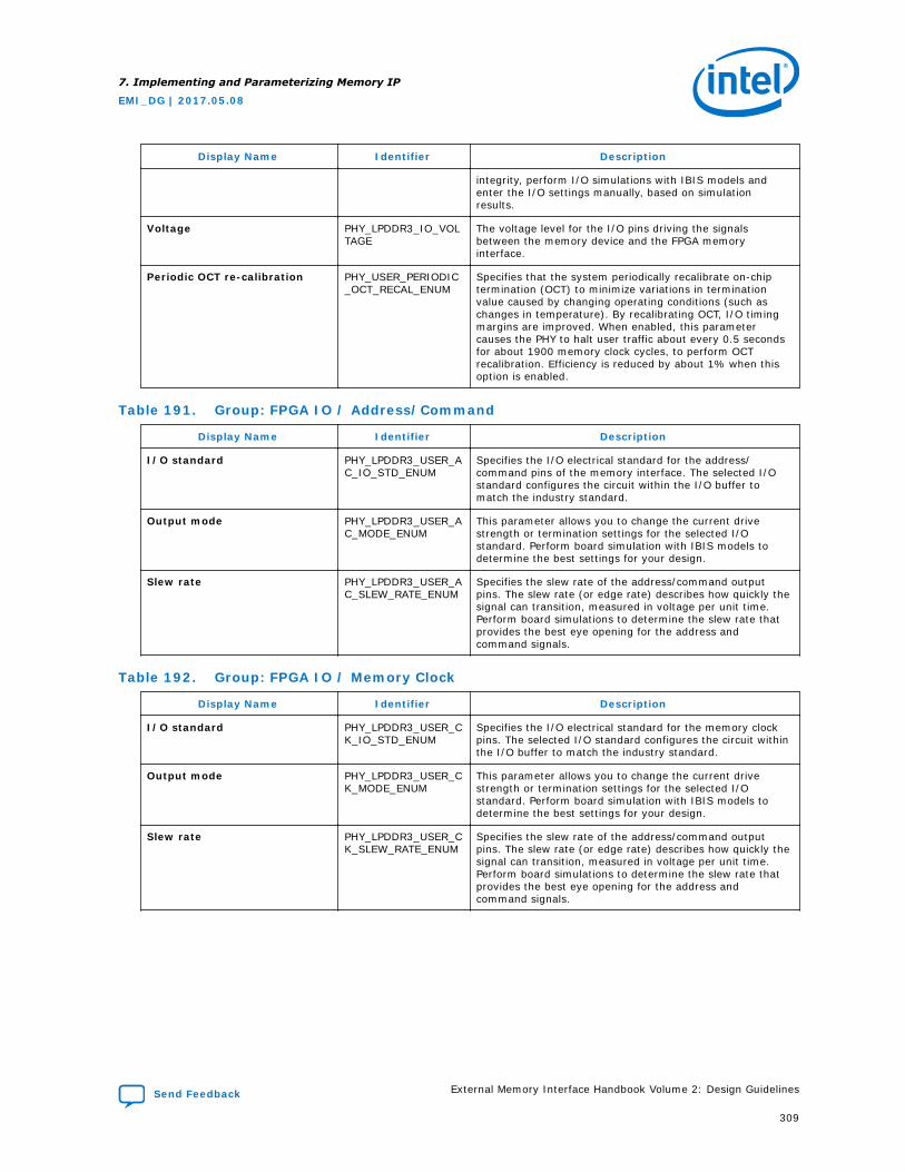
Display Name Identifier Description
integrity, perform I/O simulations with IBIS models andenter the I/O settings manually, based on simulationresults.
Voltage PHY_LPDDR3_IO_VOLTAGE
The voltage level for the I/O pins driving the signalsbetween the memory device and the FPGA memoryinterface.
Periodic OCT re-calibration PHY_USER_PERIODIC_OCT_RECAL_ENUM
Specifies that the system periodically recalibrate on-chiptermination (OCT) to minimize variations in terminationvalue caused by changing operating conditions (such aschanges in temperature). By recalibrating OCT, I/O timingmargins are improved. When enabled, this parametercauses the PHY to halt user traffic about every 0.5 secondsfor about 1900 memory clock cycles, to perform OCTrecalibration. Efficiency is reduced by about 1% when thisoption is enabled.
Table 191. Group: FPGA IO / Address/Command
Display Name Identifier Description
I/O standard PHY_LPDDR3_USER_AC_IO_STD_ENUM
Specifies the I/O electrical standard for the address/command pins of the memory interface. The selected I/Ostandard configures the circuit within the I/O buffer tomatch the industry standard.
Output mode PHY_LPDDR3_USER_AC_MODE_ENUM
This parameter allows you to change the current drivestrength or termination settings for the selected I/Ostandard. Perform board simulation with IBIS models todetermine the best settings for your design.
Slew rate PHY_LPDDR3_USER_AC_SLEW_RATE_ENUM
Specifies the slew rate of the address/command outputpins. The slew rate (or edge rate) describes how quickly thesignal can transition, measured in voltage per unit time.Perform board simulations to determine the slew rate thatprovides the best eye opening for the address andcommand signals.
Table 192. Group: FPGA IO / Memory Clock
Display Name Identifier Description
I/O standard PHY_LPDDR3_USER_CK_IO_STD_ENUM
Specifies the I/O electrical standard for the memory clockpins. The selected I/O standard configures the circuit withinthe I/O buffer to match the industry standard.
Output mode PHY_LPDDR3_USER_CK_MODE_ENUM
This parameter allows you to change the current drivestrength or termination settings for the selected I/Ostandard. Perform board simulation with IBIS models todetermine the best settings for your design.
Slew rate PHY_LPDDR3_USER_CK_SLEW_RATE_ENUM
Specifies the slew rate of the address/command outputpins. The slew rate (or edge rate) describes how quickly thesignal can transition, measured in voltage per unit time.Perform board simulations to determine the slew rate thatprovides the best eye opening for the address andcommand signals.
7. Implementing and Parameterizing Memory IP
EMI_DG | 2017.05.08
Send Feedback External Memory Interface Handbook Volume 2: Design Guidelines
309
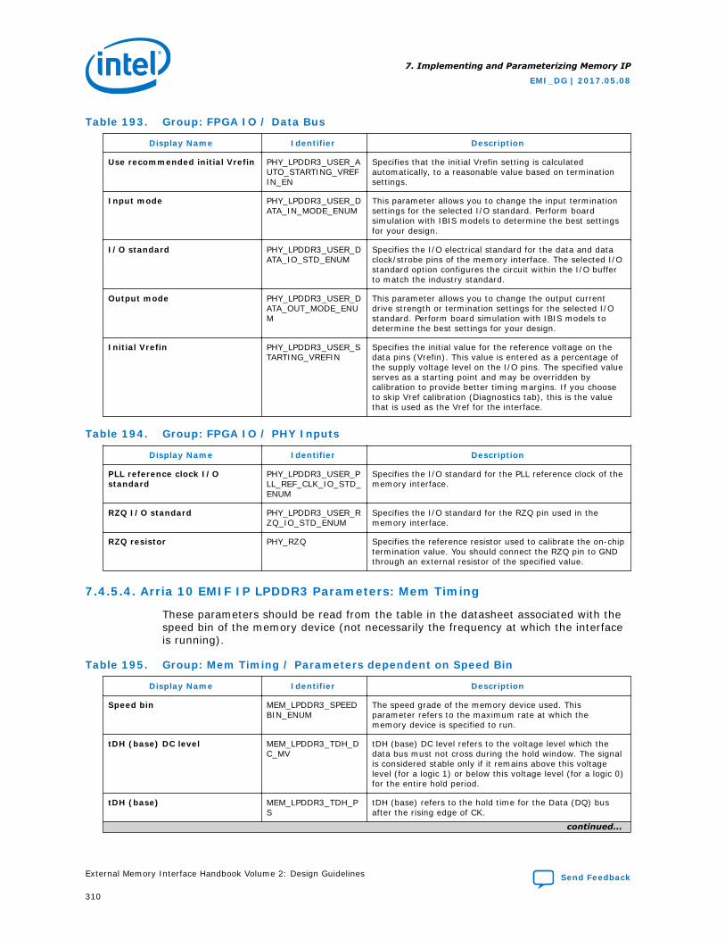
Table 193. Group: FPGA IO / Data Bus
Display Name Identifier Description
Use recommended initial Vrefin PHY_LPDDR3_USER_AUTO_STARTING_VREFIN_EN
Specifies that the initial Vrefin setting is calculatedautomatically, to a reasonable value based on terminationsettings.
Input mode PHY_LPDDR3_USER_DATA_IN_MODE_ENUM
This parameter allows you to change the input terminationsettings for the selected I/O standard. Perform boardsimulation with IBIS models to determine the best settingsfor your design.
I/O standard PHY_LPDDR3_USER_DATA_IO_STD_ENUM
Specifies the I/O electrical standard for the data and dataclock/strobe pins of the memory interface. The selected I/Ostandard option configures the circuit within the I/O bufferto match the industry standard.
Output mode PHY_LPDDR3_USER_DATA_OUT_MODE_ENUM
This parameter allows you to change the output currentdrive strength or termination settings for the selected I/Ostandard. Perform board simulation with IBIS models todetermine the best settings for your design.
Initial Vrefin PHY_LPDDR3_USER_STARTING_VREFIN
Specifies the initial value for the reference voltage on thedata pins (Vrefin). This value is entered as a percentage ofthe supply voltage level on the I/O pins. The specified valueserves as a starting point and may be overridden bycalibration to provide better timing margins. If you chooseto skip Vref calibration (Diagnostics tab), this is the valuethat is used as the Vref for the interface.
Table 194. Group: FPGA IO / PHY Inputs
Display Name Identifier Description
PLL reference clock I/Ostandard
PHY_LPDDR3_USER_PLL_REF_CLK_IO_STD_ENUM
Specifies the I/O standard for the PLL reference clock of thememory interface.
RZQ I/O standard PHY_LPDDR3_USER_RZQ_IO_STD_ENUM
Specifies the I/O standard for the RZQ pin used in thememory interface.
RZQ resistor PHY_RZQ Specifies the reference resistor used to calibrate the on-chiptermination value. You should connect the RZQ pin to GNDthrough an external resistor of the specified value.
7.4.5.4. Arria 10 EMIF IP LPDDR3 Parameters: Mem Timing
These parameters should be read from the table in the datasheet associated with thespeed bin of the memory device (not necessarily the frequency at which the interfaceis running).
Table 195. Group: Mem Timing / Parameters dependent on Speed Bin
Display Name Identifier Description
Speed bin MEM_LPDDR3_SPEEDBIN_ENUM
The speed grade of the memory device used. Thisparameter refers to the maximum rate at which thememory device is specified to run.
tDH (base) DC level MEM_LPDDR3_TDH_DC_MV
tDH (base) DC level refers to the voltage level which thedata bus must not cross during the hold window. The signalis considered stable only if it remains above this voltagelevel (for a logic 1) or below this voltage level (for a logic 0)for the entire hold period.
tDH (base) MEM_LPDDR3_TDH_PS
tDH (base) refers to the hold time for the Data (DQ) busafter the rising edge of CK.
continued...
7. Implementing and Parameterizing Memory IP
EMI_DG | 2017.05.08
External Memory Interface Handbook Volume 2: Design Guidelines Send Feedback
310
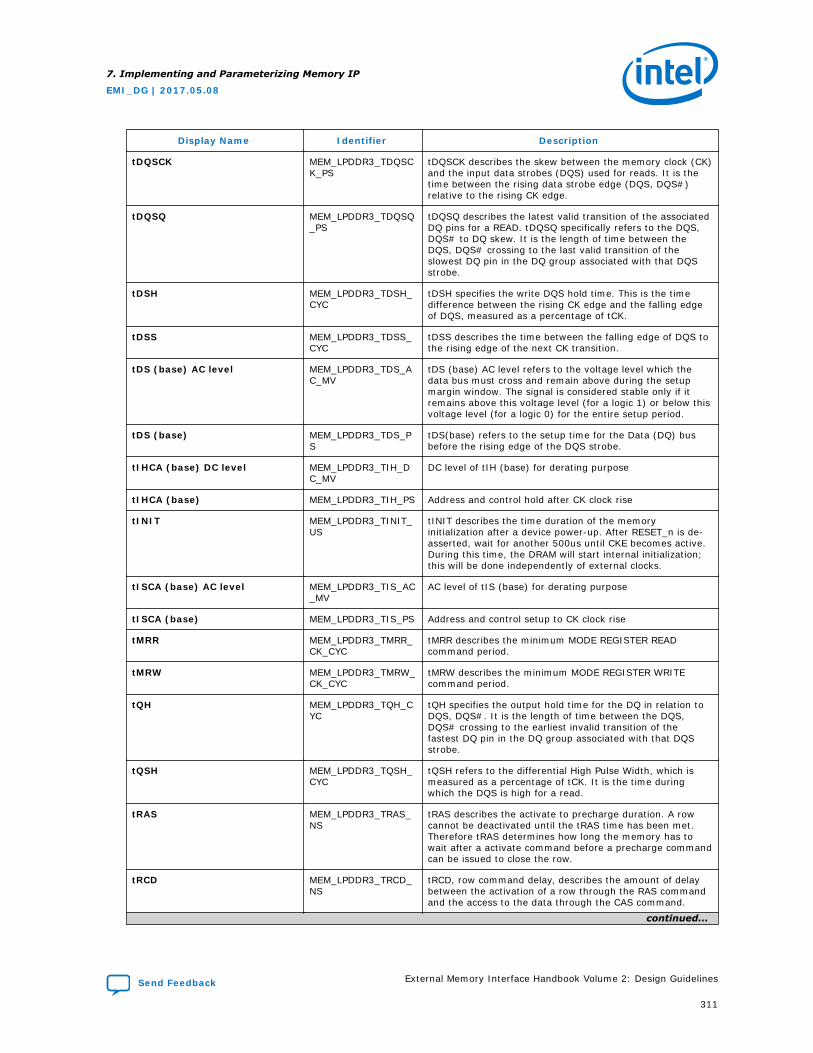
Display Name Identifier Description
tDQSCK MEM_LPDDR3_TDQSCK_PS
tDQSCK describes the skew between the memory clock (CK)and the input data strobes (DQS) used for reads. It is thetime between the rising data strobe edge (DQS, DQS#)relative to the rising CK edge.
tDQSQ MEM_LPDDR3_TDQSQ_PS
tDQSQ describes the latest valid transition of the associatedDQ pins for a READ. tDQSQ specifically refers to the DQS,DQS# to DQ skew. It is the length of time between theDQS, DQS# crossing to the last valid transition of theslowest DQ pin in the DQ group associated with that DQSstrobe.
tDSH MEM_LPDDR3_TDSH_CYC
tDSH specifies the write DQS hold time. This is the timedifference between the rising CK edge and the falling edgeof DQS, measured as a percentage of tCK.
tDSS MEM_LPDDR3_TDSS_CYC
tDSS describes the time between the falling edge of DQS tothe rising edge of the next CK transition.
tDS (base) AC level MEM_LPDDR3_TDS_AC_MV
tDS (base) AC level refers to the voltage level which thedata bus must cross and remain above during the setupmargin window. The signal is considered stable only if itremains above this voltage level (for a logic 1) or below thisvoltage level (for a logic 0) for the entire setup period.
tDS (base) MEM_LPDDR3_TDS_PS
tDS(base) refers to the setup time for the Data (DQ) busbefore the rising edge of the DQS strobe.
tIHCA (base) DC level MEM_LPDDR3_TIH_DC_MV
DC level of tIH (base) for derating purpose
tIHCA (base) MEM_LPDDR3_TIH_PS Address and control hold after CK clock rise
tINIT MEM_LPDDR3_TINIT_US
tINIT describes the time duration of the memoryinitialization after a device power-up. After RESET_n is de-asserted, wait for another 500us until CKE becomes active.During this time, the DRAM will start internal initialization;this will be done independently of external clocks.
tISCA (base) AC level MEM_LPDDR3_TIS_AC_MV
AC level of tIS (base) for derating purpose
tISCA (base) MEM_LPDDR3_TIS_PS Address and control setup to CK clock rise
tMRR MEM_LPDDR3_TMRR_CK_CYC
tMRR describes the minimum MODE REGISTER READcommand period.
tMRW MEM_LPDDR3_TMRW_CK_CYC
tMRW describes the minimum MODE REGISTER WRITEcommand period.
tQH MEM_LPDDR3_TQH_CYC
tQH specifies the output hold time for the DQ in relation toDQS, DQS#. It is the length of time between the DQS,DQS# crossing to the earliest invalid transition of thefastest DQ pin in the DQ group associated with that DQSstrobe.
tQSH MEM_LPDDR3_TQSH_CYC
tQSH refers to the differential High Pulse Width, which ismeasured as a percentage of tCK. It is the time duringwhich the DQS is high for a read.
tRAS MEM_LPDDR3_TRAS_NS
tRAS describes the activate to precharge duration. A rowcannot be deactivated until the tRAS time has been met.Therefore tRAS determines how long the memory has towait after a activate command before a precharge commandcan be issued to close the row.
tRCD MEM_LPDDR3_TRCD_NS
tRCD, row command delay, describes the amount of delaybetween the activation of a row through the RAS commandand the access to the data through the CAS command.
continued...
7. Implementing and Parameterizing Memory IP
EMI_DG | 2017.05.08
Send Feedback External Memory Interface Handbook Volume 2: Design Guidelines
311
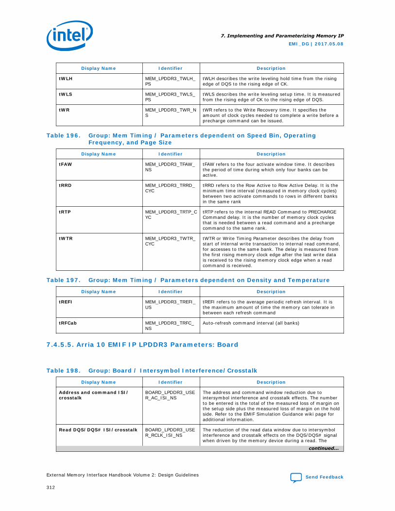
Display Name Identifier Description
tWLH MEM_LPDDR3_TWLH_PS
tWLH describes the write leveling hold time from the risingedge of DQS to the rising edge of CK.
tWLS MEM_LPDDR3_TWLS_PS
tWLS describes the write leveling setup time. It is measuredfrom the rising edge of CK to the rising edge of DQS.
tWR MEM_LPDDR3_TWR_NS
tWR refers to the Write Recovery time. It specifies theamount of clock cycles needed to complete a write before aprecharge command can be issued.
Table 196. Group: Mem Timing / Parameters dependent on Speed Bin, OperatingFrequency, and Page Size
Display Name Identifier Description
tFAW MEM_LPDDR3_TFAW_NS
tFAW refers to the four activate window time. It describesthe period of time during which only four banks can beactive.
tRRD MEM_LPDDR3_TRRD_CYC
tRRD refers to the Row Active to Row Active Delay. It is theminimum time interval (measured in memory clock cycles)between two activate commands to rows in different banksin the same rank
tRTP MEM_LPDDR3_TRTP_CYC
tRTP refers to the internal READ Command to PRECHARGECommand delay. It is the number of memory clock cyclesthat is needed between a read command and a prechargecommand to the same rank.
tWTR MEM_LPDDR3_TWTR_CYC
tWTR or Write Timing Parameter describes the delay fromstart of internal write transaction to internal read command,for accesses to the same bank. The delay is measured fromthe first rising memory clock edge after the last write datais received to the rising memory clock edge when a readcommand is received.
Table 197. Group: Mem Timing / Parameters dependent on Density and Temperature
Display Name Identifier Description
tREFI MEM_LPDDR3_TREFI_US
tREFI refers to the average periodic refresh interval. It isthe maximum amount of time the memory can tolerate inbetween each refresh command
tRFCab MEM_LPDDR3_TRFC_NS
Auto-refresh command interval (all banks)
7.4.5.5. Arria 10 EMIF IP LPDDR3 Parameters: Board
Table 198. Group: Board / Intersymbol Interference/Crosstalk
Display Name Identifier Description
Address and command ISI/crosstalk
BOARD_LPDDR3_USER_AC_ISI_NS
The address and command window reduction due tointersymbol interference and crosstalk effects. The numberto be entered is the total of the measured loss of margin onthe setup side plus the measured loss of margin on the holdside. Refer to the EMIF Simulation Guidance wiki page foradditional information.
Read DQS/DQS# ISI/crosstalk BOARD_LPDDR3_USER_RCLK_ISI_NS
The reduction of the read data window due to intersymbolinterference and crosstalk effects on the DQS/DQS# signalwhen driven by the memory device during a read. The
continued...
7. Implementing and Parameterizing Memory IP
EMI_DG | 2017.05.08
External Memory Interface Handbook Volume 2: Design Guidelines Send Feedback
312
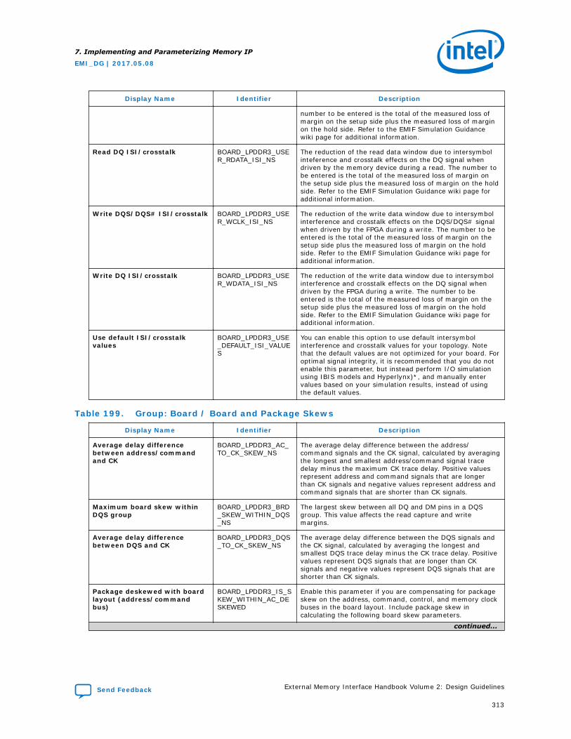
Display Name Identifier Description
number to be entered is the total of the measured loss ofmargin on the setup side plus the measured loss of marginon the hold side. Refer to the EMIF Simulation Guidancewiki page for additional information.
Read DQ ISI/crosstalk BOARD_LPDDR3_USER_RDATA_ISI_NS
The reduction of the read data window due to intersymbolinteference and crosstalk effects on the DQ signal whendriven by the memory device during a read. The number tobe entered is the total of the measured loss of margin onthe setup side plus the measured loss of margin on the holdside. Refer to the EMIF Simulation Guidance wiki page foradditional information.
Write DQS/DQS# ISI/crosstalk BOARD_LPDDR3_USER_WCLK_ISI_NS
The reduction of the write data window due to intersymbolinterference and crosstalk effects on the DQS/DQS# signalwhen driven by the FPGA during a write. The number to beentered is the total of the measured loss of margin on thesetup side plus the measured loss of margin on the holdside. Refer to the EMIF Simulation Guidance wiki page foradditional information.
Write DQ ISI/crosstalk BOARD_LPDDR3_USER_WDATA_ISI_NS
The reduction of the write data window due to intersymbolinterference and crosstalk effects on the DQ signal whendriven by the FPGA during a write. The number to beentered is the total of the measured loss of margin on thesetup side plus the measured loss of margin on the holdside. Refer to the EMIF Simulation Guidance wiki page foradditional information.
Use default ISI/crosstalkvalues
BOARD_LPDDR3_USE_DEFAULT_ISI_VALUES
You can enable this option to use default intersymbolinterference and crosstalk values for your topology. Notethat the default values are not optimized for your board. Foroptimal signal integrity, it is recommended that you do notenable this parameter, but instead perform I/O simulationusing IBIS models and Hyperlynx)*, and manually entervalues based on your simulation results, instead of usingthe default values.
Table 199. Group: Board / Board and Package Skews
Display Name Identifier Description
Average delay differencebetween address/commandand CK
BOARD_LPDDR3_AC_TO_CK_SKEW_NS
The average delay difference between the address/command signals and the CK signal, calculated by averagingthe longest and smallest address/command signal tracedelay minus the maximum CK trace delay. Positive valuesrepresent address and command signals that are longerthan CK signals and negative values represent address andcommand signals that are shorter than CK signals.
Maximum board skew withinDQS group
BOARD_LPDDR3_BRD_SKEW_WITHIN_DQS_NS
The largest skew between all DQ and DM pins in a DQSgroup. This value affects the read capture and writemargins.
Average delay differencebetween DQS and CK
BOARD_LPDDR3_DQS_TO_CK_SKEW_NS
The average delay difference between the DQS signals andthe CK signal, calculated by averaging the longest andsmallest DQS trace delay minus the CK trace delay. Positivevalues represent DQS signals that are longer than CKsignals and negative values represent DQS signals that areshorter than CK signals.
Package deskewed with boardlayout (address/commandbus)
BOARD_LPDDR3_IS_SKEW_WITHIN_AC_DESKEWED
Enable this parameter if you are compensating for packageskew on the address, command, control, and memory clockbuses in the board layout. Include package skew incalculating the following board skew parameters.
continued...
7. Implementing and Parameterizing Memory IP
EMI_DG | 2017.05.08
Send Feedback External Memory Interface Handbook Volume 2: Design Guidelines
313

Display Name Identifier Description
Package deskewed with boardlayout (DQS group)
BOARD_LPDDR3_IS_SKEW_WITHIN_DQS_DESKEWED
Enable this parameter if you are compensating for packageskew on the DQ, DQS, and DM buses in the board layout.Include package skew in calculating the following boardskew parameters.
Maximum CK delay to device BOARD_LPDDR3_MAX_CK_DELAY_NS
The maximum CK delay to device refers to the delay of thelongest CK trace from the FPGA to any device.
Maximum DQS delay to device BOARD_LPDDR3_MAX_DQS_DELAY_NS
The maximum DQS delay to device refers to the delay ofthe longest DQS trace from the FPGA to any device
Maximum system skew withinaddress/command bus
BOARD_LPDDR3_PKG_BRD_SKEW_WITHIN_AC_NS
Maximum system skew within address/command bus refersto the largest skew between the address and commandsignals.
Maximum delay differencebetween devices
BOARD_LPDDR3_SKEW_BETWEEN_DIMMS_NS
This parameter describes the largest propagation delay onthe DQ signals between ranks. For example, in a two-rankconfiguration where devices are placed in series, there is anextra propagation delay for DQ signals going to and comingback from the furthest device compared to the nearestdevice. This parameter is only applicable when there ismore than one rank.
Maximum skew between DQSgroups
BOARD_LPDDR3_SKEW_BETWEEN_DQS_NS
The largest skew between DQS signals.
7.4.5.6. Arria 10 EMIF IP LPDDR3 Parameters: Controller
Table 200. Group: Controller / Low Power Mode
Display Name Identifier Description
Auto Power-Down Cycles CTRL_LPDDR3_AUTO_POWER_DOWN_CYCS
Specifies the number of idle controller cycles after which thememory device is placed into power-down mode. You canconfigure the idle waiting time. The supported range fornumber of cycles is from 1 to 65534.
Enable Auto Power-Down CTRL_LPDDR3_AUTO_POWER_DOWN_EN
Enable this parameter to have the controller automaticallyplace the memory device into power-down mode after aspecified number of idle controller clock cycles. The idle waittime is configurable. All ranks must be idle to enter autopower-down.
Table 201. Group: Controller / Efficiency
Display Name Identifier Description
Address Ordering CTRL_LPDDR3_ADDR_ORDER_ENUM
Controls the mapping between Avalon addresses andmemory device addresses. By changing the value of thisparameter, you can change the mappings between theAvalon-MM address and the DRAM address.
Enable Auto-Precharge Control CTRL_LPDDR3_AUTO_PRECHARGE_EN
Select this parameter to enable the auto-precharge controlon the controller top level. If you assert the auto-prechargecontrol signal while requesting a read or write burst, youcan specify whether the controller should close (auto-precharge) the currently open page at the end of the reador write burst, potentially making a future access to adifferent page of the same bank faster.
Enable Reordering CTRL_LPDDR3_REORDER_EN
Enable this parameter to allow the controller to performcommand and data reordering. Reordering can improveefficiency by reducing bus turnaround time and row/bank
continued...
7. Implementing and Parameterizing Memory IP
EMI_DG | 2017.05.08
External Memory Interface Handbook Volume 2: Design Guidelines Send Feedback
314
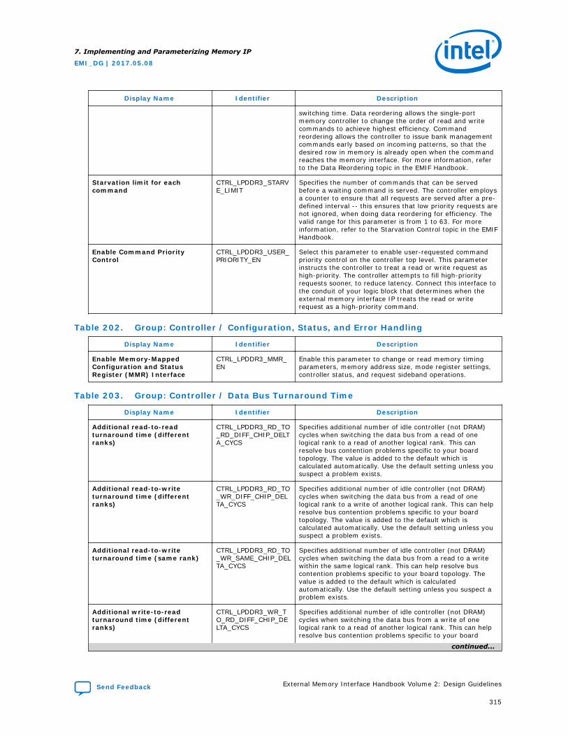
Display Name Identifier Description
switching time. Data reordering allows the single-portmemory controller to change the order of read and writecommands to achieve highest efficiency. Commandreordering allows the controller to issue bank managementcommands early based on incoming patterns, so that thedesired row in memory is already open when the commandreaches the memory interface. For more information, referto the Data Reordering topic in the EMIF Handbook.
Starvation limit for eachcommand
CTRL_LPDDR3_STARVE_LIMIT
Specifies the number of commands that can be servedbefore a waiting command is served. The controller employsa counter to ensure that all requests are served after a pre-defined interval -- this ensures that low priority requests arenot ignored, when doing data reordering for efficiency. Thevalid range for this parameter is from 1 to 63. For moreinformation, refer to the Starvation Control topic in the EMIFHandbook.
Enable Command PriorityControl
CTRL_LPDDR3_USER_PRIORITY_EN
Select this parameter to enable user-requested commandpriority control on the controller top level. This parameterinstructs the controller to treat a read or write request ashigh-priority. The controller attempts to fill high-priorityrequests sooner, to reduce latency. Connect this interface tothe conduit of your logic block that determines when theexternal memory interface IP treats the read or writerequest as a high-priority command.
Table 202. Group: Controller / Configuration, Status, and Error Handling
Display Name Identifier Description
Enable Memory-MappedConfiguration and StatusRegister (MMR) Interface
CTRL_LPDDR3_MMR_EN
Enable this parameter to change or read memory timingparameters, memory address size, mode register settings,controller status, and request sideband operations.
Table 203. Group: Controller / Data Bus Turnaround Time
Display Name Identifier Description
Additional read-to-readturnaround time (differentranks)
CTRL_LPDDR3_RD_TO_RD_DIFF_CHIP_DELTA_CYCS
Specifies additional number of idle controller (not DRAM)cycles when switching the data bus from a read of onelogical rank to a read of another logical rank. This canresolve bus contention problems specific to your boardtopology. The value is added to the default which iscalculated automatically. Use the default setting unless yoususpect a problem exists.
Additional read-to-writeturnaround time (differentranks)
CTRL_LPDDR3_RD_TO_WR_DIFF_CHIP_DELTA_CYCS
Specifies additional number of idle controller (not DRAM)cycles when switching the data bus from a read of onelogical rank to a write of another logical rank. This can helpresolve bus contention problems specific to your boardtopology. The value is added to the default which iscalculated automatically. Use the default setting unless yoususpect a problem exists.
Additional read-to-writeturnaround time (same rank)
CTRL_LPDDR3_RD_TO_WR_SAME_CHIP_DELTA_CYCS
Specifies additional number of idle controller (not DRAM)cycles when switching the data bus from a read to a writewithin the same logical rank. This can help resolve buscontention problems specific to your board topology. Thevalue is added to the default which is calculatedautomatically. Use the default setting unless you suspect aproblem exists.
Additional write-to-readturnaround time (differentranks)
CTRL_LPDDR3_WR_TO_RD_DIFF_CHIP_DELTA_CYCS
Specifies additional number of idle controller (not DRAM)cycles when switching the data bus from a write of onelogical rank to a read of another logical rank. This can helpresolve bus contention problems specific to your board
continued...
7. Implementing and Parameterizing Memory IP
EMI_DG | 2017.05.08
Send Feedback External Memory Interface Handbook Volume 2: Design Guidelines
315
Display Name Identifier Description
topology. The value is added to the default which iscalculated automatically. Use the default setting unless yoususpect a problem exists.
Additional write-to-readturnaround time (same rank)
CTRL_LPDDR3_WR_TO_RD_SAME_CHIP_DELTA_CYCS
Specifies additional number of idle controller (not DRAM)cycles when switching the data bus from a write to a readwithin the same logical rank. This can help resolve buscontention problems specific to your board topology. Thevalue is added to the default which is calculatedautomatically. Use the default setting unless you suspect aproblem exists.
Additional write-to-writeturnaround time (differentranks)
CTRL_LPDDR3_WR_TO_WR_DIFF_CHIP_DELTA_CYCS
Specifies additional number of idle controller (not DRAM)cycles when switching the data bus from a write of onelogical rank to a write of another logical rank. This can helpresolve bus contention problems specific to your boardtopology. The value is added to the default which iscalculated automatically. Use the default setting unless yoususpect a problem exists.
7.4.5.7. Arria 10 EMIF IP LPDDR3 Parameters: Diagnostics
Table 204. Group: Diagnostics / Simulation Options
Display Name Identifier Description
Abstract phy for fast simulation DIAG_LPDDR3_ABSTRACT_PHY
Specifies that the system use Abstract PHY for simulation.Abstract PHY replaces the PHY with a model for fastsimulation and can reduce simulation time by 2-3 times.Abstract PHY is available for certain protocols and devicefamilies, and only when you select Skip Calibration.
Calibration mode DIAG_SIM_CAL_MODE_ENUM
Specifies whether to skip memory interface calibrationduring simulation, or to simulate the full calibration process.Simulating the full calibration process can take hours (oreven days), depending on the width and depth of thememory interface. You can achieve much faster simulationtimes by skipping the calibration process, but that is onlyexpected to work when the memory model is ideal and theinterconnect delays are zero. If you enable this parameter,the interface still performs some memory initializationbefore starting normal operations. Abstract PHY issupported with skip calibration.
Table 205. Group: Diagnostics / Calibration Debug Options
Display Name Identifier Description
Enable Daisy-Chaining forQuartus Prime EMIF DebugToolkit/On-Chip Debug Port
DIAG_EXPORT_SEQ_AVALON_MASTER
Specifies that the IP export an Avalon-MM master interface(cal_debug_out) which can connect to the cal_debuginterface of other EMIF cores residing in the same I/Ocolumn. This parameter applies only if the EMIF DebugToolkit or On-Chip Debug Port is enabled. Refer to theDebugging Multiple EMIFs wiki page for more informationabout debugging multiple EMIFs.
Quartus Prime EMIF DebugToolkit/On-Chip Debug Port
DIAG_EXPORT_SEQ_AVALON_SLAVE
Specifies the connectivity of an Avalon slave interface foruse by the Quartus Prime EMIF Debug Toolkit or user corelogic. If you set this parameter to "Disabled," no debugfeatures are enabled. If you set this parameter to "Export,"an Avalon slave interface named "cal_debug" is exportedfrom the IP. To use this interface with the EMIF DebugToolkit, you must instantiate and connect an EMIF debug
continued...
7. Implementing and Parameterizing Memory IP
EMI_DG | 2017.05.08
External Memory Interface Handbook Volume 2: Design Guidelines Send Feedback
316
Display Name Identifier Description
interface IP core to it, or connect it to the cal_debug_outinterface of another EMIF core. If you select "Add EMIFDebug Interface", an EMIF debug interface componentcontaining a JTAG Avalon Master is connected to the debugport, allowing the core to be accessed by the EMIF DebugToolkit. Only one EMIF debug interface should beinstantiated per I/O column. You can chain additional EMIFor PHYLite cores to the first by enabling the "Enable Daisy-Chaining for Quartus Prime EMIF Debug Toolkit/On-ChipDebug Port" option for all cores in the chain, and selecting"Export" for the "Quartus Prime EMIF Debug Toolkit/On-ChipDebug Port" option on all cores after the first.
Interface ID DIAG_INTERFACE_ID Identifies interfaces within the I/O column, for use by theEMIF Debug Toolkit and the On-Chip Debug Port. InterfaceIDs should be unique among EMIF cores within the sameI/O column. If the Quartus Prime EMIF Debug Toolkit/On-Chip Debug Port parameter is set to Disabled, the interfaceID is unused.
Skip address/commanddeskew calibration
DIAG_LPDDR3_SKIP_CA_DESKEW
Specifies to skip the address/command deskew calibrationstage. Address/command deskew performs per-bit deskewfor the address and command pins.
Skip address/commandleveling calibration
DIAG_LPDDR3_SKIP_CA_LEVEL
Specifies to skip the address/command leveling stageduring calibration. Address/command leveling attempts tocenter the memory clock edge against CS# by adjustingdelay elements inside the PHY, and then applying the samedelay offset to the rest of the address and command pins.
Use Soft NIOS Processor forOn-Chip Debug
DIAG_SOFT_NIOS_MODE
Enables a soft Nios processor as a peripheral component toaccess the On-Chip Debug Port. Only one interface in acolumn can activate this option.
Table 206. Group: Diagnostics / Example Design
Display Name Identifier Description
Enable In-System-Sources-and-Probes
DIAG_EX_DESIGN_ISSP_EN
Enables In-System-Sources-and-Probes in the exampledesign for common debug signals, such as calibration statusor example traffic generator per-bit status. This parametermust be enabled if you want to do driver margining.
Number of core clocks sharingslaves to instantiate in theexample design
DIAG_EX_DESIGN_NUM_OF_SLAVES
Specifies the number of core clock sharing slaves toinstantiate in the example design. This parameter appliesonly if you set the "Core clocks sharing" parameter in the"General" tab to Master or Slave.
Table 207. Group: Diagnostics / Traffic Generator
Display Name Identifier Description
Bypass the default trafficpattern
DIAG_BYPASS_DEFAULT_PATTERN
Specifies that the controller/interface bypass the trafficgenerator 2.0 default pattern after reset. If you do notenable this parameter, the traffic generator does not asserta pass or fail status until the generator is configured andsignaled to start by its Avalon configuration interface.
Bypass the traffic generatorrepeated-writes/repeated-reads test pattern
DIAG_BYPASS_REPEAT_STAGE
Specifies that the controller/interface bypass the trafficgenerator's repeat test stage. If you do not enable thisparameter, every write and read is repeated several times.
Bypass the traffic generatorstress pattern
DIAG_BYPASS_STRESS_STAGE
Specifies that the controller/interface bypass the trafficgenerator's stress pattern stage. (Stress patterns are meantto create worst-case signal integrity patterns on the datapins.) If you do not enable this parameter, the traffic
continued...
7. Implementing and Parameterizing Memory IP
EMI_DG | 2017.05.08
Send Feedback External Memory Interface Handbook Volume 2: Design Guidelines
317

Display Name Identifier Description
generator does not assert a pass or fail status until thegenerator is configured and signaled to start by its Avalonconfiguration interface.
Bypass the user-configuredtraffic stage
DIAG_BYPASS_USER_STAGE
Specifies that the controller/interface bypass the user-configured traffic generator's pattern after reset. If you donot enable this parameter, the traffic generator does notassert a pass or fail status until the generator is configuredand signaled to start by its Avalon configuration interface.Configuration can be done by connecting to the trafficgenerator via the EMIF Debug Toolkit, or by using customlogic connected to the Avalon-MM configuration slave porton the traffic generator. Configuration can also be simulatedusing the example testbench provided in thealtera_emif_avl_tg_2_tb.sv file.
Run diagnostic on infinite testduration
DIAG_INFI_TG2_ERR_TEST
Specifies that the traffic generator run indefinitely until thefirst error is detected.
Export Traffic Generator 2.0configuration interface
DIAG_TG_AVL_2_EXPORT_CFG_INTERFACE
Specifies that the IP export an Avalon-MM slave port forconfiguring the Traffic Generator. This is required only if youare configuring the traffic generator through user logic andnot through through the EMIF Debug Toolkit.
Use configurable Avalon trafficgenerator 2.0
DIAG_USE_TG_AVL_2 This option allows users to add the new configurable Avalontraffic generator to the example design.
Table 208. Group: Diagnostics / Performance
Display Name Identifier Description
Enable Efficiency Monitor DIAG_EFFICIENCY_MONITOR
Adds an Efficiency Monitor component to the Avalon-MMinterface of the memory controller, allowing you to viewefficiency statistics of the interface. You can access theefficiency statistics using the EMIF Debug Toolkit.
Table 209. Group: Diagnostics / Miscellaneous
Display Name Identifier Description
Use short Qsys interface names SHORT_QSYS_INTERFACE_NAMES
Specifies the use of short interface names, for improvedusability and consistency with other Qsys components. Ifthis parameter is disabled, the names of Qsys interfacesexposed by the IP will include the type and direction of theinterface. Long interface names are supported forbackward-compatibility and will be removed in a futurerelease.
7.4.5.8. Arria 10 EMIF IP LPDDR3 Parameters: Example Designs
Table 210. Group: Example Designs / Available Example Designs
Display Name Identifier Description
Select design EX_DESIGN_GUI_LPDDR3_SEL_DESIGN
Specifies the creation of a full Quartus Prime project,instantiating an external memory interface and an exampletraffic generator, according to your parameterization. Afterthe design is created, you can specify the target device andpin location assignments, run a full compilation, verifytiming closure, and test the interface on your board usingthe programming file created by the Quartus Primeassembler. The 'Generate Example Design' button lets yougenerate simulation or synthesis file sets.
7. Implementing and Parameterizing Memory IP
EMI_DG | 2017.05.08
External Memory Interface Handbook Volume 2: Design Guidelines Send Feedback
318

Table 211. Group: Example Designs / Example Design Files
Display Name Identifier Description
Simulation EX_DESIGN_GUI_LPDDR3_GEN_SIM
Specifies that the 'Generate Example Design' button createall necessary file sets for simulation. Expect a shortadditional delay as the file set is created. If you do notenable this parameter, simulation file sets are not created.Instead, the output directory will contain the ed_sim.qsysfile which holds Qsys details of the simulation exampledesign, and a make_sim_design.tcl file with othercorresponding tcl files. You can run make_sim_design.tclfrom a command line to generate the simulation exampledesign. The generated example designs for varioussimulators are stored in the /sim sub-directory.
Synthesis EX_DESIGN_GUI_LPDDR3_GEN_SYNTH
Specifies that the 'Generate Example Design' button createall necessary file sets for synthesis. Expect a shortadditional delay as the file set is created. If you do notenable this parameter, synthesis file sets are not created.Instead, the output directory will contain the ed_synth.qsysfile which holds Qsys details of the synthesis exampledesign, and a make_qii_design.tcl script with othercorresponding tcl files. You can run make_qii_design.tclfrom a command line to generate the synthesis exampledesign. The generated example design is stored in the /qiisub-directory.
Table 212. Group: Example Designs / Generated HDL Format
Display Name Identifier Description
Simulation HDL format EX_DESIGN_GUI_LPDDR3_HDL_FORMAT
This option lets you choose the format of HDL in whichgenerated simulation files are created.
Table 213. Group: Example Designs / Target Development Kit
Display Name Identifier Description
Select board EX_DESIGN_GUI_LPDDR3_TARGET_DEV_KIT
Specifies that when you select a development kit with amemory module, the generated example design contains allsettings and fixed pin assignments to run on the selectedboard. You must select a development kit preset togenerate a working example design for the specifieddevelopment kit. Any IP settings not applied directly from adevelopment kit preset will not have guaranteed resultswhen testing the development kit. To exclude hardwaresupport of the example design, select 'none' from the'Select board' pull down menu. When you apply adevelopment kit preset, all IP parameters are automaticallyset appropriately to match the selected preset. If you wantto save your current settings, you should do so before youapply the preset. You can save your settings under adifferent name using File->Save as.
7.4.5.9. About Memory Presets
Presets help simplify the process of copying memory parameter values from memorydevice data sheets to the EMIF parameter editor.
For DDRx protocols, the memory presets are named using the following convention:
PROTOCOL-SPEEDBIN LATENCY FORMAT-AND-TOPOLOGY CAPACITY (INTERNAL-ORGANIZATION)
7. Implementing and Parameterizing Memory IP
EMI_DG | 2017.05.08
Send Feedback External Memory Interface Handbook Volume 2: Design Guidelines
319

For example, the preset named DDR4-2666U CL18 Component 1CS 2Gb (512Mbx 4) refers to a DDR4 x4 component rated at the DDR4-2666U JEDEC speed bin, withnominal CAS latency of 18 cycles, one chip-select, and a total memory space of 2Gb.The JEDEC memory specification defines multiple speed bins for a given frequency(that is, DDR4-2666U and DDR4-2666V). You may be able to determine the exactspeed bin implemented by your memory device using its nominal latency. When indoubt, contact your memory vendor.
For RLDRAMx and QDRx protocols, the memory presets are named based on thevendor's device part number.
When the preset list does not contain the exact configuration required, you can stillminimize data entry by selecting the preset closest to your configuration and thenmodify parameters as required.
Prior to production you should always review the parameter values to ensure that theymatch your memory device data sheet, regardless of whether a preset is used or not.Incorrect memory parameters can cause functional failures.
7.4.6. Arria 10 EMIF IP QDR-IV Parameters
The Arria 10 EMIF IP parameter editor allows you to parameterize settings for theArria 10 EMIF IP.
The text window at the bottom of the parameter editor displays information about thememory interface, as well as warning and error messages. You should correct anyerrors indicated in this window before clicking the Finish button.
Note: Default settings are the minimum required to achieve timing, and may vary dependingon memory protocol.
The following tables describe the parameterization settings available in the parametereditor for the Arria 10 EMIF IP.
7.4.6.1. Arria 10 EMIF IP QDR-IV Parameters: General
Table 214. Group: General / FPGA
Display Name Identifier Description
Speed grade PHY_FPGA_SPEEDGRADE_GUI
Indicates the device speed grade, and whether it is anengineering sample (ES) or production device. This value isbased on the device that you select in the parameter editor.If you do not specify a device, the system assumes adefault value. Ensure that you always specify the correctdevice during IP generation, otherwise your IP may notwork in hardware.
Table 215. Group: General / Interface
Display Name Identifier Description
Configuration PHY_CONFIG_ENUM Specifies the configuration of the memory interface. Theavailable options depend on the protocol in use. Optionsinclude Hard PHY and Hard Controller, Hard PHY and Soft
continued...
7. Implementing and Parameterizing Memory IP
EMI_DG | 2017.05.08
External Memory Interface Handbook Volume 2: Design Guidelines Send Feedback
320

Display Name Identifier Description
Controller, or Hard PHY only. If you select Hard PHY only,the AFI interface is exported to allow connection of acustom memory controller or third-party IP.
Instantiate two controllerssharing a Ping Pong PHY
PHY_PING_PONG_EN Specifies the instantiation of two identical memorycontrollers that share an address/command bus through theuse of Ping Pong PHY. This parameter is available only if youspecify the Hard PHY and Hard Controller option. When thisparameter is enabled, the IP exposes two independentAvalon interfaces to the user logic, and a single externalmemory interface with double width for the data bus andthe CS#, CKE, ODT, and CK/CK# signals.
Table 216. Group: General / Clocks
Display Name Identifier Description
Core clocks sharing PHY_CORE_CLKS_SHARING_ENUM
When a design contains multiple interfaces of the sameprotocol, rate, frequency, and PLL reference clock source,they can share a common set of core clock domains. Bysharing core clock domains, they reduce clock networkusage and avoid clock synchronization logic between theinterfaces. To share core clocks, denote one of theinterfaces as "Master", and the remaining interfaces as"Slave". In the RTL, connect the clks_sharing_master_outsignal from the master interface to theclks_sharing_slave_in signal of all the slave interfaces. Bothmaster and slave interfaces still expose their own outputclock ports in the RTL (for example, emif_usr_clk, afi_clk),but the physical signals are equivalent, hence it does notmatter whether a clock port from a master or a slave isused. As the combined width of all interfaces sharing thesame core clock increases, you may encounter timingclosure difficulty for transfers between the FPGA core andthe periphery.
Memory clock frequency PHY_MEM_CLK_FREQ_MHZ
Specifies the operating frequency of the memory interfacein MHz. If you change the memory frequency, you shouldupdate the memory latency parameters on the "Memory"tab and the memory timing parameters on the "MemTiming" tab.
Use recommended PLLreference clock frequency
PHY_QDR4_DEFAULT_REF_CLK_FREQ
Specifies that the PLL reference clock frequency isautomatically calculated for best performance. If you wantto specify a different PLL reference clock frequency, uncheckthe check box for this parameter.
Clock rate of user logic PHY_RATE_ENUM Specifies the relationship between the user logic clockfrequency and the memory clock frequency. For example, ifthe memory clock sent from the FPGA to the memorydevice is toggling at 800MHz, a quarter-rate interfacemeans that the user logic in the FPGA runs at 200MHz.
PLL reference clock frequency PHY_REF_CLK_FREQ_MHZ
Specifies the PLL reference clock frequency. You mustconfigure this parameter only if you do not check the "Userecommended PLL reference clock frequency" parameter. Toconfigure this parameter, select a valid PLL reference clockfrequency from the list. The values in the list can change ifyou change the memory interface frequency and/or the
continued...
7. Implementing and Parameterizing Memory IP
EMI_DG | 2017.05.08
Send Feedback External Memory Interface Handbook Volume 2: Design Guidelines
321
Display Name Identifier Description
clock rate of the user logic. For best jitter performance, youshould use the fastest possible PLL reference clockfrequency.
PLL reference clock jitter PHY_REF_CLK_JITTER_PS
Specifies the peak-to-peak jitter on the PLL reference clocksource. The clock source of the PLL reference clock mustmeet or exceed the following jitter requirements: 10ps peakto peak, or 1.42ps RMS at 1e-12 BER, 1.22ps at 1e-16 BER.
Specify additional core clocksbased on existing PLL
PLL_ADD_EXTRA_CLKS
Displays additional parameters allowing you to createadditional output clocks based on the existing PLL. Thisparameter provides an alternative clock-generationmechanism for when your design exhausts available PLLresources. The additional output clocks that you create canbe fed into the core. Clock signals created with thisparameter are synchronous to each other, but asynchronousto the memory interface core clock domains (such asemif_usr_clk or afi_clk). You must follow proper clock-domain-crossing techniques when transferring data betweenclock domains.
Table 217. Group: General / Additional Core Clocks
Display Name Identifier Description
Number of additional coreclocks
PLL_USER_NUM_OF_EXTRA_CLKS
Specifies the number of additional output clocks to createfrom the PLL.
7.4.6.2. Arria 10 EMIF IP QDR-IV Parameters: Memory
Table 218. Group: Memory / Topology
Display Name Identifier Description
Address width MEM_QDR4_ADDR_WIDTH
Number of address pins.
DINVA / DINVB width MEM_QDR4_DINV_PER_PORT_WIDTH
Number of DINV pins for port A or B of the memoryinterface. Automatically calculated based on the DQ widthper device and whether width expansion is enabled. Twomemory input pins without expansion and four pins withwidth expansion.
DKA / DKB width MEM_QDR4_DK_PER_PORT_WIDTH
Number of DK clock pairs for port A or B of the memoryinterface. Automatically calculated based on the DQ widthper device and whether width expansion is enabled. Twomemory input pins without expansion and four pins withwidth expansion.
DQ width per device MEM_QDR4_DQ_PER_PORT_PER_DEVICE
Specifies number of DQ pins per RLDRAM3 device andnumber of DQ pins per port per QDR IV device. Availablewidths for DQ are x18 and x36.
continued...
7. Implementing and Parameterizing Memory IP
EMI_DG | 2017.05.08
External Memory Interface Handbook Volume 2: Design Guidelines Send Feedback
322

Display Name Identifier Description
DQA / DQB width MEM_QDR4_DQ_PER_PORT_WIDTH
Number of DQ pins for port A or B of the memory interface.Automatically calculated based on the DQ width per deviceand whether width expansion is enabled. The interfacesupports a width expansion configuration up to 72-bits
QKA / QKB width MEM_QDR4_QK_PER_PORT_WIDTH
Number of QK clock pairs for port A or B of the memoryinterface. Automatically calculated based on the DQ widthper device and whether width expansion is enabled. Twomemory input pins without expansion and four pins withwidth expansion.
Enable width expansion MEM_QDR4_WIDTH_EXPANDED
Indicates whether to combine two memory devices todouble the data bus width. With two devices, the interfacesupports a width expansion configuration up to 72-bits. Forwidth expansion configuration, the address and controlsignals are routed to 2 devices.
Table 219. Group: Memory / Configuration Register Settings
Display Name Identifier Description
ODT (Address/Command) MEM_QDR4_AC_ODT_MODE_ENUM
Determines the configuration register setting that controlsthe address/command ODT setting.
Address bus inversion MEM_QDR4_ADDR_INV_ENA
Enable address bus inversion. AINV are all active high atmemory device.
ODT (Clock) MEM_QDR4_CK_ODT_MODE_ENUM
Determines the configuration register setting that controlsthe clock ODT setting.
Data bus inversion MEM_QDR4_DATA_INV_ENA
Enable data bus inversion for DQ pins. DINVA[1:0] andDINVB[1:0] are all active high. When set to 1, thecorresponding bus is inverted at memory device. If the datainversion feature is programmed to be OFF, then the DINVA/DINVB output bits will always be driven to 0.
ODT (Data) MEM_QDR4_DATA_ODT_MODE_ENUM
Determines the configuration register setting that controlsthe data ODT setting.
Output drive (pull-down) MEM_QDR4_PD_OUTPUT_DRIVE_MODE_ENUM
Determines the configuration register setting that controlsthe pull-down output drive setting.
Output drive (pull-up) MEM_QDR4_PU_OUTPUT_DRIVE_MODE_ENUM
Determines the configuration register setting that controlsthe pull-up output drive setting.
7.4.6.3. Arria 10 EMIF IP QDR-IV Parameters: FPGA I/O
You should use Hyperlynx* or similar simulators to determine the best settings foryour board. Refer to the EMIF Simulation Guidance wiki page for additionalinformation.
Table 220. Group: FPGA IO / FPGA IO Settings
Display Name Identifier Description
Use default I/O settings PHY_QDR4_DEFAULT_IO
Specifies that a legal set of I/O settings are automaticallyselected. The default I/O settings are not necessarilyoptimized for a specific board. To achieve optimal signal
continued...
7. Implementing and Parameterizing Memory IP
EMI_DG | 2017.05.08
Send Feedback External Memory Interface Handbook Volume 2: Design Guidelines
323

Display Name Identifier Description
integrity, perform I/O simulations with IBIS models andenter the I/O settings manually, based on simulationresults.
Voltage PHY_QDR4_IO_VOLTAGE
The voltage level for the I/O pins driving the signalsbetween the memory device and the FPGA memoryinterface.
Periodic OCT re-calibration PHY_USER_PERIODIC_OCT_RECAL_ENUM
Specifies that the system periodically recalibrate on-chiptermination (OCT) to minimize variations in terminationvalue caused by changing operating conditions (such aschanges in temperature). By recalibrating OCT, I/O timingmargins are improved. When enabled, this parametercauses the PHY to halt user traffic about every 0.5 secondsfor about 1900 memory clock cycles, to perform OCTrecalibration. Efficiency is reduced by about 1% when thisoption is enabled.
Table 221. Group: FPGA IO / Address/Command
Display Name Identifier Description
I/O standard PHY_QDR4_USER_AC_IO_STD_ENUM
Specifies the I/O electrical standard for the address/command pins of the memory interface. The selected I/Ostandard configures the circuit within the I/O buffer tomatch the industry standard.
Output mode PHY_QDR4_USER_AC_MODE_ENUM
This parameter allows you to change the current drivestrength or termination settings for the selected I/Ostandard. Perform board simulation with IBIS models todetermine the best settings for your design.
Slew rate PHY_QDR4_USER_AC_SLEW_RATE_ENUM
Specifies the slew rate of the address/command outputpins. The slew rate (or edge rate) describes how quickly thesignal can transition, measured in voltage per unit time.Perform board simulations to determine the slew rate thatprovides the best eye opening for the address andcommand signals.
Table 222. Group: FPGA IO / Memory Clock
Display Name Identifier Description
I/O standard PHY_QDR4_USER_CK_IO_STD_ENUM
Specifies the I/O electrical standard for the memory clockpins. The selected I/O standard configures the circuit withinthe I/O buffer to match the industry standard.
Output mode PHY_QDR4_USER_CK_MODE_ENUM
This parameter allows you to change the current drivestrength or termination settings for the selected I/Ostandard. Perform board simulation with IBIS models todetermine the best settings for your design.
Slew rate PHY_QDR4_USER_CK_SLEW_RATE_ENUM
Specifies the slew rate of the address/command outputpins. The slew rate (or edge rate) describes how quickly thesignal can transition, measured in voltage per unit time.Perform board simulations to determine the slew rate thatprovides the best eye opening for the address andcommand signals.
7. Implementing and Parameterizing Memory IP
EMI_DG | 2017.05.08
External Memory Interface Handbook Volume 2: Design Guidelines Send Feedback
324
Table 223. Group: FPGA IO / Data Bus
Display Name Identifier Description
Use recommended initial Vrefin PHY_QDR4_USER_AUTO_STARTING_VREFIN_EN
Specifies that the initial Vrefin setting is calculatedautomatically, to a reasonable value based on terminationsettings.
Input mode PHY_QDR4_USER_DATA_IN_MODE_ENUM
This parameter allows you to change the input terminationsettings for the selected I/O standard. Perform boardsimulation with IBIS models to determine the best settingsfor your design.
I/O standard PHY_QDR4_USER_DATA_IO_STD_ENUM
Specifies the I/O electrical standard for the data and dataclock/strobe pins of the memory interface. The selected I/Ostandard option configures the circuit within the I/O bufferto match the industry standard.
Output mode PHY_QDR4_USER_DATA_OUT_MODE_ENUM
This parameter allows you to change the output currentdrive strength or termination settings for the selected I/Ostandard. Perform board simulation with IBIS models todetermine the best settings for your design.
Initial Vrefin PHY_QDR4_USER_STARTING_VREFIN
Specifies the initial value for the reference voltage on thedata pins (Vrefin). This value is entered as a percentage ofthe supply voltage level on the I/O pins. The specified valueserves as a starting point and may be overridden bycalibration to provide better timing margins. If you chooseto skip Vref calibration (Diagnostics tab), this is the valuethat is used as the Vref for the interface.
Table 224. Group: FPGA IO / PHY Inputs
Display Name Identifier Description
PLL reference clock I/Ostandard
PHY_QDR4_USER_PLL_REF_CLK_IO_STD_ENUM
Specifies the I/O standard for the PLL reference clock of thememory interface.
RZQ I/O standard PHY_QDR4_USER_RZQ_IO_STD_ENUM
Specifies the I/O standard for the RZQ pin used in thememory interface.
RZQ resistor PHY_RZQ Specifies the reference resistor used to calibrate the on-chiptermination value. You should connect the RZQ pin to GNDthrough an external resistor of the specified value.
7.4.6.4. Arria 10 EMIF IP QDR-IV Parameters: Mem Timing
These parameters should be read from the table in the datasheet associated with thespeed bin of the memory device (not necessarily the frequency at which the interfaceis running).
Table 225. Group: Mem Timing / Parameters dependent on Speed Bin
Display Name Identifier Description
Speed bin MEM_QDR4_SPEEDBIN_ENUM
The speed grade of the memory device used. Thisparameter refers to the maximum rate at which thememory device is specified to run.
tASH MEM_QDR4_TASH_PS tASH provides the setup/hold window requirement for theaddress bus in relation to the CK clock. Because theindividual signals in the address bus may not be perfectlyaligned with each other, this parameter describes theintersection window for all the individual address signalssetup/hold margins.
continued...
7. Implementing and Parameterizing Memory IP
EMI_DG | 2017.05.08
Send Feedback External Memory Interface Handbook Volume 2: Design Guidelines
325
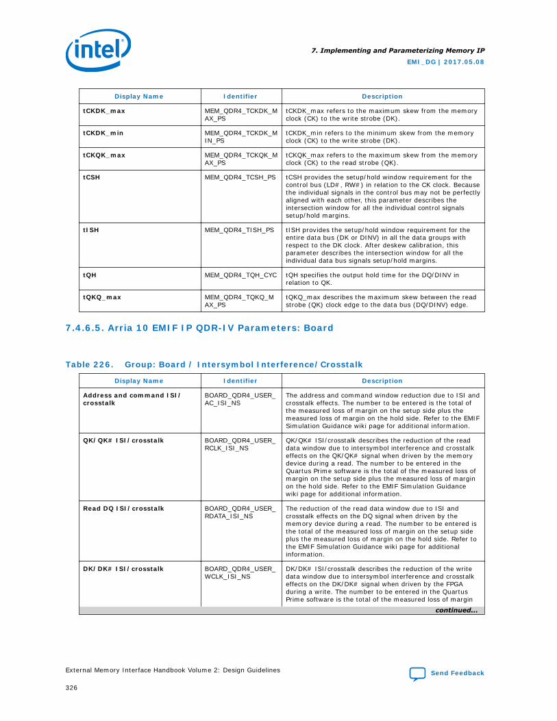
Display Name Identifier Description
tCKDK_max MEM_QDR4_TCKDK_MAX_PS
tCKDK_max refers to the maximum skew from the memoryclock (CK) to the write strobe (DK).
tCKDK_min MEM_QDR4_TCKDK_MIN_PS
tCKDK_min refers to the minimum skew from the memoryclock (CK) to the write strobe (DK).
tCKQK_max MEM_QDR4_TCKQK_MAX_PS
tCKQK_max refers to the maximum skew from the memoryclock (CK) to the read strobe (QK).
tCSH MEM_QDR4_TCSH_PS tCSH provides the setup/hold window requirement for thecontrol bus (LD#, RW#) in relation to the CK clock. Becausethe individual signals in the control bus may not be perfectlyaligned with each other, this parameter describes theintersection window for all the individual control signalssetup/hold margins.
tISH MEM_QDR4_TISH_PS tISH provides the setup/hold window requirement for theentire data bus (DK or DINV) in all the data groups withrespect to the DK clock. After deskew calibration, thisparameter describes the intersection window for all theindividual data bus signals setup/hold margins.
tQH MEM_QDR4_TQH_CYC tQH specifies the output hold time for the DQ/DINV inrelation to QK.
tQKQ_max MEM_QDR4_TQKQ_MAX_PS
tQKQ_max describes the maximum skew between the readstrobe (QK) clock edge to the data bus (DQ/DINV) edge.
7.4.6.5. Arria 10 EMIF IP QDR-IV Parameters: Board
Table 226. Group: Board / Intersymbol Interference/Crosstalk
Display Name Identifier Description
Address and command ISI/crosstalk
BOARD_QDR4_USER_AC_ISI_NS
The address and command window reduction due to ISI andcrosstalk effects. The number to be entered is the total ofthe measured loss of margin on the setup side plus themeasured loss of margin on the hold side. Refer to the EMIFSimulation Guidance wiki page for additional information.
QK/QK# ISI/crosstalk BOARD_QDR4_USER_RCLK_ISI_NS
QK/QK# ISI/crosstalk describes the reduction of the readdata window due to intersymbol interference and crosstalkeffects on the QK/QK# signal when driven by the memorydevice during a read. The number to be entered in theQuartus Prime software is the total of the measured loss ofmargin on the setup side plus the measured loss of marginon the hold side. Refer to the EMIF Simulation Guidancewiki page for additional information.
Read DQ ISI/crosstalk BOARD_QDR4_USER_RDATA_ISI_NS
The reduction of the read data window due to ISI andcrosstalk effects on the DQ signal when driven by thememory device during a read. The number to be entered isthe total of the measured loss of margin on the setup sideplus the measured loss of margin on the hold side. Refer tothe EMIF Simulation Guidance wiki page for additionalinformation.
DK/DK# ISI/crosstalk BOARD_QDR4_USER_WCLK_ISI_NS
DK/DK# ISI/crosstalk describes the reduction of the writedata window due to intersymbol interference and crosstalkeffects on the DK/DK# signal when driven by the FPGAduring a write. The number to be entered in the QuartusPrime software is the total of the measured loss of margin
continued...
7. Implementing and Parameterizing Memory IP
EMI_DG | 2017.05.08
External Memory Interface Handbook Volume 2: Design Guidelines Send Feedback
326

Display Name Identifier Description
on the setup side plus the measured loss of margin on thehold side. Refer to the EMIF Simulation Guidance wiki pagefor additional information.
Write DQ ISI/crosstalk BOARD_QDR4_USER_WDATA_ISI_NS
The reduction of the write data window due to intersymbolinterference and crosstalk effects on the DQ signal whendriven by the FPGA during a write. The number to beentered is the total of the measured loss of margin on thesetup side plus the measured loss of margin on the holdside. Refer to the EMIF Simulation Guidance wiki page foradditional information.
Use default ISI/crosstalkvalues
BOARD_QDR4_USE_DEFAULT_ISI_VALUES
You can enable this option to use default intersymbolinterference and crosstalk values for your topology. Notethat the default values are not optimized for your board. Foroptimal signal integrity, it is recommended that you do notenable this parameter, but instead perform I/O simulationusing IBIS models and Hyperlynx*, and manually entervalues based on your simulation results, instead of usingthe default values.
Table 227. Group: Board / Board and Package Skews
Display Name Identifier Description
Average delay differencebetween address/commandand CK
BOARD_QDR4_AC_TO_CK_SKEW_NS
The average delay difference between the address/command signals and the CK signal, calculated by averagingthe longest and smallest address/command signal tracedelay minus the maximum CK trace delay. Positive valuesrepresent address and command signals that are longerthan CK signals and negative values represent address andcommand signals that are shorter than CK signals.
Average delay differencebetween DK and CK
BOARD_QDR4_DK_TO_CK_SKEW_NS
This parameter describes the average delay differencebetween the DK signals and the CK signal, calculated byaveraging the longest and smallest DK trace delay minusthe CK trace delay. Positive values represent DK signals thatare longer than CK signals and negative values representDK signals that are shorter than CK signals.
Package deskewed with boardlayout (address/commandbus)
BOARD_QDR4_IS_SKEW_WITHIN_AC_DESKEWED
Enable this parameter if you are compensating for packageskew on the address, command, control, and memory clockbuses in the board layout. Include package skew incalculating the following board skew parameters.
Package deskewed with boardlayout (QK group)
BOARD_QDR4_IS_SKEW_WITHIN_QK_DESKEWED
If you are compensating for package skew on the QK bus inthe board layout (hence checking the box here), pleaseinclude package skew in calculating the following boardskew parameters.
Maximum CK delay to device BOARD_QDR4_MAX_CK_DELAY_NS
The maximum CK delay to device refers to the delay of thelongest CK trace from the FPGA to any device.
Maximum DK delay to device BOARD_QDR4_MAX_DK_DELAY_NS
The maximum DK delay to device refers to the delay of thelongest DK trace from the FPGA to any device.
Maximum system skew withinaddress/command bus
BOARD_QDR4_PKG_BRD_SKEW_WITHIN_AC_NS
Maximum system skew within address/command bus refersto the largest skew between the address and commandsignals.
Maximum system skew withinQK group
BOARD_QDR4_PKG_BRD_SKEW_WITHIN_QK_NS
Maximum system skew within QK group refers to the largestskew between all DQ and DM pins in a QK group. This valuecan affect the read capture and write margins.
Maximum delay differencebetween devices
BOARD_QDR4_SKEW_BETWEEN_DIMMS_NS
This parameter describes the largest propagation delay onthe DQ signals between ranks. For example, in a two-rankconfiguration where devices are placed in series, there is anextra propagation delay for DQ signals going to and coming
continued...
7. Implementing and Parameterizing Memory IP
EMI_DG | 2017.05.08
Send Feedback External Memory Interface Handbook Volume 2: Design Guidelines
327
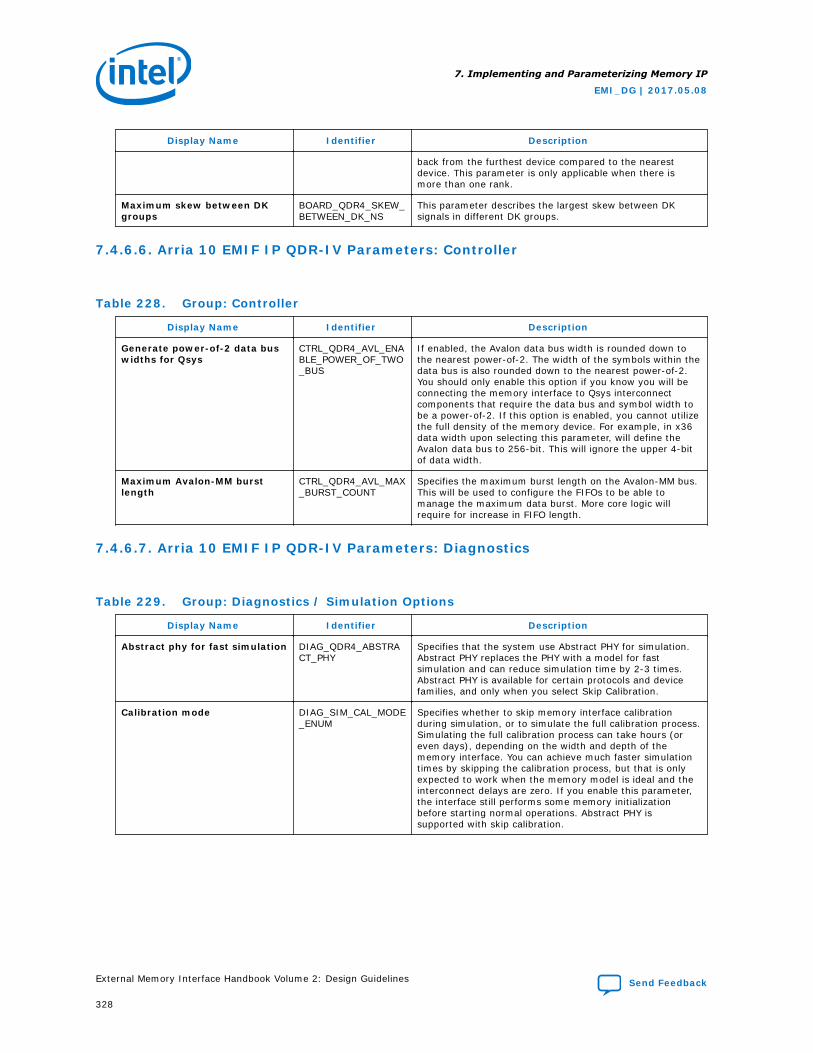
Display Name Identifier Description
back from the furthest device compared to the nearestdevice. This parameter is only applicable when there ismore than one rank.
Maximum skew between DKgroups
BOARD_QDR4_SKEW_BETWEEN_DK_NS
This parameter describes the largest skew between DKsignals in different DK groups.
7.4.6.6. Arria 10 EMIF IP QDR-IV Parameters: Controller
Table 228. Group: Controller
Display Name Identifier Description
Generate power-of-2 data buswidths for Qsys
CTRL_QDR4_AVL_ENABLE_POWER_OF_TWO_BUS
If enabled, the Avalon data bus width is rounded down tothe nearest power-of-2. The width of the symbols within thedata bus is also rounded down to the nearest power-of-2.You should only enable this option if you know you will beconnecting the memory interface to Qsys interconnectcomponents that require the data bus and symbol width tobe a power-of-2. If this option is enabled, you cannot utilizethe full density of the memory device. For example, in x36data width upon selecting this parameter, will define theAvalon data bus to 256-bit. This will ignore the upper 4-bitof data width.
Maximum Avalon-MM burstlength
CTRL_QDR4_AVL_MAX_BURST_COUNT
Specifies the maximum burst length on the Avalon-MM bus.This will be used to configure the FIFOs to be able tomanage the maximum data burst. More core logic willrequire for increase in FIFO length.
7.4.6.7. Arria 10 EMIF IP QDR-IV Parameters: Diagnostics
Table 229. Group: Diagnostics / Simulation Options
Display Name Identifier Description
Abstract phy for fast simulation DIAG_QDR4_ABSTRACT_PHY
Specifies that the system use Abstract PHY for simulation.Abstract PHY replaces the PHY with a model for fastsimulation and can reduce simulation time by 2-3 times.Abstract PHY is available for certain protocols and devicefamilies, and only when you select Skip Calibration.
Calibration mode DIAG_SIM_CAL_MODE_ENUM
Specifies whether to skip memory interface calibrationduring simulation, or to simulate the full calibration process.Simulating the full calibration process can take hours (oreven days), depending on the width and depth of thememory interface. You can achieve much faster simulationtimes by skipping the calibration process, but that is onlyexpected to work when the memory model is ideal and theinterconnect delays are zero. If you enable this parameter,the interface still performs some memory initializationbefore starting normal operations. Abstract PHY issupported with skip calibration.
7. Implementing and Parameterizing Memory IP
EMI_DG | 2017.05.08
External Memory Interface Handbook Volume 2: Design Guidelines Send Feedback
328
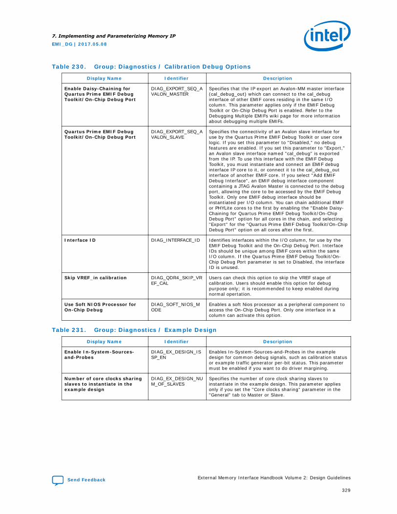
Table 230. Group: Diagnostics / Calibration Debug Options
Display Name Identifier Description
Enable Daisy-Chaining forQuartus Prime EMIF DebugToolkit/On-Chip Debug Port
DIAG_EXPORT_SEQ_AVALON_MASTER
Specifies that the IP export an Avalon-MM master interface(cal_debug_out) which can connect to the cal_debuginterface of other EMIF cores residing in the same I/Ocolumn. This parameter applies only if the EMIF DebugToolkit or On-Chip Debug Port is enabled. Refer to theDebugging Multiple EMIFs wiki page for more informationabout debugging multiple EMIFs.
Quartus Prime EMIF DebugToolkit/On-Chip Debug Port
DIAG_EXPORT_SEQ_AVALON_SLAVE
Specifies the connectivity of an Avalon slave interface foruse by the Quartus Prime EMIF Debug Toolkit or user corelogic. If you set this parameter to "Disabled," no debugfeatures are enabled. If you set this parameter to "Export,"an Avalon slave interface named "cal_debug" is exportedfrom the IP. To use this interface with the EMIF DebugToolkit, you must instantiate and connect an EMIF debuginterface IP core to it, or connect it to the cal_debug_outinterface of another EMIF core. If you select "Add EMIFDebug Interface", an EMIF debug interface componentcontaining a JTAG Avalon Master is connected to the debugport, allowing the core to be accessed by the EMIF DebugToolkit. Only one EMIF debug interface should beinstantiated per I/O column. You can chain additional EMIFor PHYLite cores to the first by enabling the "Enable Daisy-Chaining for Quartus Prime EMIF Debug Toolkit/On-ChipDebug Port" option for all cores in the chain, and selecting"Export" for the "Quartus Prime EMIF Debug Toolkit/On-ChipDebug Port" option on all cores after the first.
Interface ID DIAG_INTERFACE_ID Identifies interfaces within the I/O column, for use by theEMIF Debug Toolkit and the On-Chip Debug Port. InterfaceIDs should be unique among EMIF cores within the sameI/O column. If the Quartus Prime EMIF Debug Toolkit/On-Chip Debug Port parameter is set to Disabled, the interfaceID is unused.
Skip VREF_in calibration DIAG_QDR4_SKIP_VREF_CAL
Users can check this option to skip the VREF stage ofcalibration. Users should enable this option for debugpurpose only; it is recommended to keep enabled duringnormal opertation.
Use Soft NIOS Processor forOn-Chip Debug
DIAG_SOFT_NIOS_MODE
Enables a soft Nios processor as a peripheral component toaccess the On-Chip Debug Port. Only one interface in acolumn can activate this option.
Table 231. Group: Diagnostics / Example Design
Display Name Identifier Description
Enable In-System-Sources-and-Probes
DIAG_EX_DESIGN_ISSP_EN
Enables In-System-Sources-and-Probes in the exampledesign for common debug signals, such as calibration statusor example traffic generator per-bit status. This parametermust be enabled if you want to do driver margining.
Number of core clocks sharingslaves to instantiate in theexample design
DIAG_EX_DESIGN_NUM_OF_SLAVES
Specifies the number of core clock sharing slaves toinstantiate in the example design. This parameter appliesonly if you set the "Core clocks sharing" parameter in the"General" tab to Master or Slave.
7. Implementing and Parameterizing Memory IP
EMI_DG | 2017.05.08
Send Feedback External Memory Interface Handbook Volume 2: Design Guidelines
329
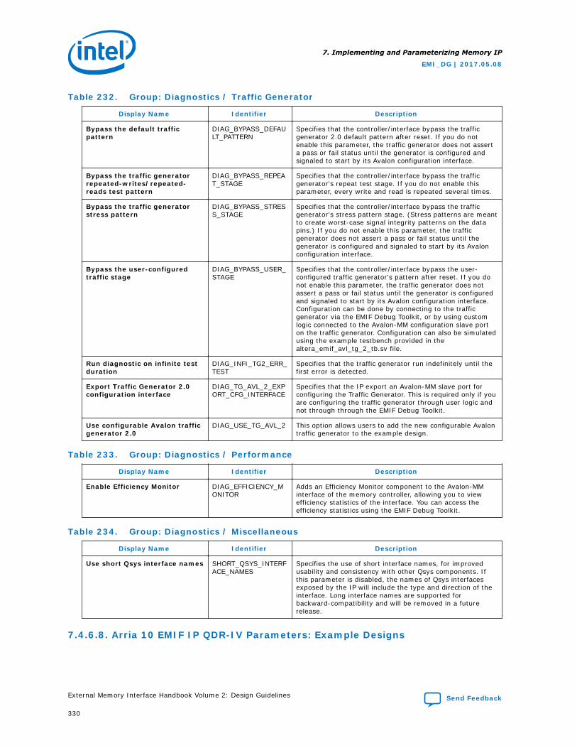
Table 232. Group: Diagnostics / Traffic Generator
Display Name Identifier Description
Bypass the default trafficpattern
DIAG_BYPASS_DEFAULT_PATTERN
Specifies that the controller/interface bypass the trafficgenerator 2.0 default pattern after reset. If you do notenable this parameter, the traffic generator does not asserta pass or fail status until the generator is configured andsignaled to start by its Avalon configuration interface.
Bypass the traffic generatorrepeated-writes/repeated-reads test pattern
DIAG_BYPASS_REPEAT_STAGE
Specifies that the controller/interface bypass the trafficgenerator's repeat test stage. If you do not enable thisparameter, every write and read is repeated several times.
Bypass the traffic generatorstress pattern
DIAG_BYPASS_STRESS_STAGE
Specifies that the controller/interface bypass the trafficgenerator's stress pattern stage. (Stress patterns are meantto create worst-case signal integrity patterns on the datapins.) If you do not enable this parameter, the trafficgenerator does not assert a pass or fail status until thegenerator is configured and signaled to start by its Avalonconfiguration interface.
Bypass the user-configuredtraffic stage
DIAG_BYPASS_USER_STAGE
Specifies that the controller/interface bypass the user-configured traffic generator's pattern after reset. If you donot enable this parameter, the traffic generator does notassert a pass or fail status until the generator is configuredand signaled to start by its Avalon configuration interface.Configuration can be done by connecting to the trafficgenerator via the EMIF Debug Toolkit, or by using customlogic connected to the Avalon-MM configuration slave porton the traffic generator. Configuration can also be simulatedusing the example testbench provided in thealtera_emif_avl_tg_2_tb.sv file.
Run diagnostic on infinite testduration
DIAG_INFI_TG2_ERR_TEST
Specifies that the traffic generator run indefinitely until thefirst error is detected.
Export Traffic Generator 2.0configuration interface
DIAG_TG_AVL_2_EXPORT_CFG_INTERFACE
Specifies that the IP export an Avalon-MM slave port forconfiguring the Traffic Generator. This is required only if youare configuring the traffic generator through user logic andnot through through the EMIF Debug Toolkit.
Use configurable Avalon trafficgenerator 2.0
DIAG_USE_TG_AVL_2 This option allows users to add the new configurable Avalontraffic generator to the example design.
Table 233. Group: Diagnostics / Performance
Display Name Identifier Description
Enable Efficiency Monitor DIAG_EFFICIENCY_MONITOR
Adds an Efficiency Monitor component to the Avalon-MMinterface of the memory controller, allowing you to viewefficiency statistics of the interface. You can access theefficiency statistics using the EMIF Debug Toolkit.
Table 234. Group: Diagnostics / Miscellaneous
Display Name Identifier Description
Use short Qsys interface names SHORT_QSYS_INTERFACE_NAMES
Specifies the use of short interface names, for improvedusability and consistency with other Qsys components. Ifthis parameter is disabled, the names of Qsys interfacesexposed by the IP will include the type and direction of theinterface. Long interface names are supported forbackward-compatibility and will be removed in a futurerelease.
7.4.6.8. Arria 10 EMIF IP QDR-IV Parameters: Example Designs
7. Implementing and Parameterizing Memory IP
EMI_DG | 2017.05.08
External Memory Interface Handbook Volume 2: Design Guidelines Send Feedback
330
Table 235. Group: Example Designs / Available Example Designs
Display Name Identifier Description
Select design EX_DESIGN_GUI_QDR4_SEL_DESIGN
Specifies the creation of a full Quartus Prime project,instantiating an external memory interface and an exampletraffic generator, according to your parameterization. Afterthe design is created, you can specify the target device andpin location assignments, run a full compilation, verifytiming closure, and test the interface on your board usingthe programming file created by the Quartus Primeassembler. The 'Generate Example Design' button lets yougenerate simulation or synthesis file sets.
Table 236. Group: Example Designs / Example Design Files
Display Name Identifier Description
Simulation EX_DESIGN_GUI_QDR4_GEN_SIM
Specifies that the 'Generate Example Design' button createall necessary file sets for simulation. Expect a shortadditional delay as the file set is created. If you do notenable this parameter, simulation file sets are not created.Instead, the output directory will contain the ed_sim.qsysfile which holds Qsys details of the simulation exampledesign, and a make_sim_design.tcl file with othercorresponding tcl files. You can run make_sim_design.tclfrom a command line to generate the simulation exampledesign. The generated example designs for varioussimulators are stored in the /sim sub-directory.
Synthesis EX_DESIGN_GUI_QDR4_GEN_SYNTH
Specifies that the 'Generate Example Design' button createall necessary file sets for synthesis. Expect a shortadditional delay as the file set is created. If you do notenable this parameter, synthesis file sets are not created.Instead, the output directory will contain the ed_synth.qsysfile which holds Qsys details of the synthesis exampledesign, and a make_qii_design.tcl script with othercorresponding tcl files. You can run make_qii_design.tclfrom a command line to generate the synthesis exampledesign. The generated example design is stored in the /qiisub-directory.
Table 237. Group: Example Designs / Generated HDL Format
Display Name Identifier Description
Simulation HDL format EX_DESIGN_GUI_QDR4_HDL_FORMAT
This option lets you choose the format of HDL in whichgenerated simulation files are created.
Table 238. Group: Example Designs / Target Development Kit
Display Name Identifier Description
Select board EX_DESIGN_GUI_QDR4_TARGET_DEV_KIT
Specifies that when you select a development kit with amemory module, the generated example design contains allsettings and fixed pin assignments to run on the selectedboard. You must select a development kit preset togenerate a working example design for the specifieddevelopment kit. Any IP settings not applied directly from adevelopment kit preset will not have guaranteed resultswhen testing the development kit. To exclude hardwaresupport of the example design, select 'none' from the'Select board' pull down menu. When you apply adevelopment kit preset, all IP parameters are automaticallyset appropriately to match the selected preset. If you wantto save your current settings, you should do so before youapply the preset. You can save your settings under adifferent name using File->Save as.
7. Implementing and Parameterizing Memory IP
EMI_DG | 2017.05.08
Send Feedback External Memory Interface Handbook Volume 2: Design Guidelines
331

7.4.6.9. About Memory Presets
Presets help simplify the process of copying memory parameter values from memorydevice data sheets to the EMIF parameter editor.
For DDRx protocols, the memory presets are named using the following convention:
PROTOCOL-SPEEDBIN LATENCY FORMAT-AND-TOPOLOGY CAPACITY (INTERNAL-ORGANIZATION)
For example, the preset named DDR4-2666U CL18 Component 1CS 2Gb (512Mbx 4) refers to a DDR4 x4 component rated at the DDR4-2666U JEDEC speed bin, withnominal CAS latency of 18 cycles, one chip-select, and a total memory space of 2Gb.The JEDEC memory specification defines multiple speed bins for a given frequency(that is, DDR4-2666U and DDR4-2666V). You may be able to determine the exactspeed bin implemented by your memory device using its nominal latency. When indoubt, contact your memory vendor.
For RLDRAMx and QDRx protocols, the memory presets are named based on thevendor's device part number.
When the preset list does not contain the exact configuration required, you can stillminimize data entry by selecting the preset closest to your configuration and thenmodify parameters as required.
Prior to production you should always review the parameter values to ensure that theymatch your memory device data sheet, regardless of whether a preset is used or not.Incorrect memory parameters can cause functional failures.
7.4.7. Arria 10 EMIF IP QDR II/II+/II+ Xtreme Parameters
The Arria 10 EMIF IP parameter editor allows you to parameterize settings for theArria 10 EMIF IP.
The text window at the bottom of the parameter editor displays information about thememory interface, as well as warning and error messages. You should correct anyerrors indicated in this window before clicking the Finish button.
Note: Default settings are the minimum required to achieve timing, and may vary dependingon memory protocol.
The following tables describe the parameterization settings available in the parametereditor for the Arria 10 EMIF IP.
7.4.7.1. Arria 10 EMIF IP QDR II/II+/II+ Xtreme Parameters: General
Table 239. Group: General / FPGA
Display Name Identifier Description
Speed grade PHY_FPGA_SPEEDGRADE_GUI
Indicates the device speed grade, and whether it is anengineering sample (ES) or production device. This value isbased on the device that you select in the parameter editor.If you do not specify a device, the system assumes adefault value. Ensure that you always specify the correctdevice during IP generation, otherwise your IP may notwork in hardware.
7. Implementing and Parameterizing Memory IP
EMI_DG | 2017.05.08
External Memory Interface Handbook Volume 2: Design Guidelines Send Feedback
332
Table 240. Group: General / Interface
Display Name Identifier Description
Configuration PHY_CONFIG_ENUM Specifies the configuration of the memory interface. Theavailable options depend on the protocol in use. Optionsinclude Hard PHY and Hard Controller, Hard PHY and SoftController, or Hard PHY only. If you select Hard PHY only,the AFI interface is exported to allow connection of acustom memory controller or third-party IP.
Instantiate two controllerssharing a Ping Pong PHY
PHY_PING_PONG_EN Specifies the instantiation of two identical memorycontrollers that share an address/command bus through theuse of Ping Pong PHY. This parameter is available only if youspecify the Hard PHY and Hard Controller option. When thisparameter is enabled, the IP exposes two independentAvalon interfaces to the user logic, and a single externalmemory interface with double width for the data bus andthe CS#, CKE, ODT, and CK/CK# signals.
Table 241. Group: General / Clocks
Display Name Identifier Description
Core clocks sharing PHY_CORE_CLKS_SHARING_ENUM
When a design contains multiple interfaces of the sameprotocol, rate, frequency, and PLL reference clock source,they can share a common set of core clock domains. Bysharing core clock domains, they reduce clock networkusage and avoid clock synchronization logic between theinterfaces. To share core clocks, denote one of theinterfaces as "Master", and the remaining interfaces as"Slave". In the RTL, connect the clks_sharing_master_outsignal from the master interface to theclks_sharing_slave_in signal of all the slave interfaces. Bothmaster and slave interfaces still expose their own outputclock ports in the RTL (for example, emif_usr_clk, afi_clk),but the physical signals are equivalent, hence it does notmatter whether a clock port from a master or a slave isused. As the combined width of all interfaces sharing thesame core clock increases, you may encounter timingclosure difficulty for transfers between the FPGA core andthe periphery.
Memory clock frequency PHY_MEM_CLK_FREQ_MHZ
Specifies the operating frequency of the memory interfacein MHz. If you change the memory frequency, you shouldupdate the memory latency parameters on the "Memory"tab and the memory timing parameters on the "MemTiming" tab.
Use recommended PLLreference clock frequency
PHY_QDR2_DEFAULT_REF_CLK_FREQ
Specifies that the PLL reference clock frequency isautomatically calculated for best performance. If you wantto specify a different PLL reference clock frequency, uncheckthe check box for this parameter.
Clock rate of user logic PHY_RATE_ENUM Specifies the relationship between the user logic clockfrequency and the memory clock frequency. For example, ifthe memory clock sent from the FPGA to the memorydevice is toggling at 800MHz, a quarter-rate interfacemeans that the user logic in the FPGA runs at 200MHz.
PLL reference clock frequency PHY_REF_CLK_FREQ_MHZ
Specifies the PLL reference clock frequency. You mustconfigure this parameter only if you do not check the "Userecommended PLL reference clock frequency" parameter. Toconfigure this parameter, select a valid PLL reference clockfrequency from the list. The values in the list can change ifyou change the memory interface frequency and/or the
continued...
7. Implementing and Parameterizing Memory IP
EMI_DG | 2017.05.08
Send Feedback External Memory Interface Handbook Volume 2: Design Guidelines
333
Display Name Identifier Description
clock rate of the user logic. For best jitter performance, youshould use the fastest possible PLL reference clockfrequency.
PLL reference clock jitter PHY_REF_CLK_JITTER_PS
Specifies the peak-to-peak jitter on the PLL reference clocksource. The clock source of the PLL reference clock mustmeet or exceed the following jitter requirements: 10ps peakto peak, or 1.42ps RMS at 1e-12 BER, 1.22ps at 1e-16 BER.
Specify additional core clocksbased on existing PLL
PLL_ADD_EXTRA_CLKS
Displays additional parameters allowing you to createadditional output clocks based on the existing PLL. Thisparameter provides an alternative clock-generationmechanism for when your design exhausts available PLLresources. The additional output clocks that you create canbe fed into the core. Clock signals created with thisparameter are synchronous to each other, but asynchronousto the memory interface core clock domains (such asemif_usr_clk or afi_clk). You must follow proper clock-domain-crossing techniques when transferring data betweenclock domains.
Table 242. Group: General / Additional Core Clocks
Display Name Identifier Description
Number of additional coreclocks
PLL_USER_NUM_OF_EXTRA_CLKS
Specifies the number of additional output clocks to createfrom the PLL.
7.4.7.2. Arria 10 EMIF IP QDR II/II+/II+ Xtreme Parameters: Memory
Table 243. Group: Memory / Topology
Display Name Identifier Description
Address width MEM_QDR2_ADDR_WIDTH
Number of address pins.
Burst length MEM_QDR2_BL Burst length of the memory device.
Enable BWS# pins MEM_QDR2_BWS_EN Indicates whether the interface uses the BWS#( Byte WriteSelect) pins. If enabled, 1 BWS# pin for every 9 D pins willbe added.
BWS# width MEM_QDR2_BWS_N_WIDTH
Number of BWS# (Byte Write Select) pins of the memoryinterface. Automatically calculated based on the data widthper device and whether width expansion is enabled. BWS#pins are used to select which byte is written into the deviceduring the current portion of the write operations. Bytes notwritten remain unaltered.
CQ width MEM_QDR2_CQ_WIDTH
Width of the CQ (read strobe) clock on the memory device.
Data width per device MEM_QDR2_DATA_PER_DEVICE
Number of D and Q pins per QDR II device.
continued...
7. Implementing and Parameterizing Memory IP
EMI_DG | 2017.05.08
External Memory Interface Handbook Volume 2: Design Guidelines Send Feedback
334
Display Name Identifier Description
Data width MEM_QDR2_DATA_WIDTH
Number of D and Q pins of the memory interface.Automatically calculated based on the D and Q width perdevice and whether width expansion is enabled.
K width MEM_QDR2_K_WIDTH Width of the K (address, command and write strobe) clockon the memory device.
Enable width expansion MEM_QDR2_WIDTH_EXPANDED
Indicates whether to combine two memory devices todouble the data bus width. With two devices, the interfacesupports a width expansion configuration up to 72-bits. Forwidth expansion configuration, the address and controlsignals are routed to 2 devices.
7.4.7.3. Arria 10 EMIF IP QDR II/II+/II+ Xtreme Parameters: FPGA I/O
You should use Hyperlynx* or similar simulators to determine the best settings foryour board. Refer to the EMIF Simulation Guidance wiki page for additionalinformation.
Table 244. Group: FPGA IO / FPGA IO Settings
Display Name Identifier Description
Use default I/O settings PHY_QDR2_DEFAULT_IO
Specifies that a legal set of I/O settings are automaticallyselected. The default I/O settings are not necessarilyoptimized for a specific board. To achieve optimal signalintegrity, perform I/O simulations with IBIS models andenter the I/O settings manually, based on simulationresults.
Voltage PHY_QDR2_IO_VOLTAGE
The voltage level for the I/O pins driving the signalsbetween the memory device and the FPGA memoryinterface.
Periodic OCT re-calibration PHY_USER_PERIODIC_OCT_RECAL_ENUM
Specifies that the system periodically recalibrate on-chiptermination (OCT) to minimize variations in terminationvalue caused by changing operating conditions (such aschanges in temperature). By recalibrating OCT, I/O timingmargins are improved. When enabled, this parametercauses the PHY to halt user traffic about every 0.5 secondsfor about 1900 memory clock cycles, to perform OCTrecalibration. Efficiency is reduced by about 1% when thisoption is enabled.
Table 245. Group: FPGA IO / Address/Command
Display Name Identifier Description
I/O standard PHY_QDR2_USER_AC_IO_STD_ENUM
Specifies the I/O electrical standard for the address/command pins of the memory interface. The selected I/Ostandard configures the circuit within the I/O buffer tomatch the industry standard.
Output mode PHY_QDR2_USER_AC_MODE_ENUM
This parameter allows you to change the current drivestrength or termination settings for the selected I/Ostandard. Perform board simulation with IBIS models todetermine the best settings for your design.
Slew rate PHY_QDR2_USER_AC_SLEW_RATE_ENUM
Specifies the slew rate of the address/command outputpins. The slew rate (or edge rate) describes how quickly thesignal can transition, measured in voltage per unit time.Perform board simulations to determine the slew rate thatprovides the best eye opening for the address andcommand signals.
7. Implementing and Parameterizing Memory IP
EMI_DG | 2017.05.08
Send Feedback External Memory Interface Handbook Volume 2: Design Guidelines
335
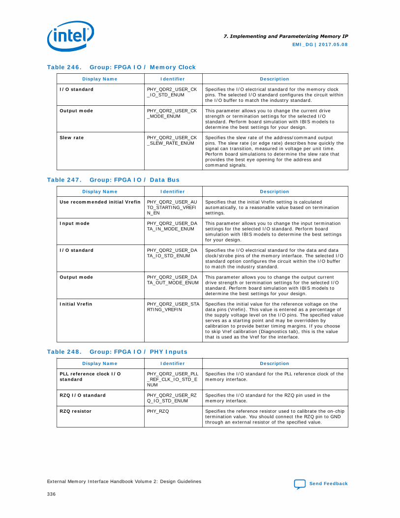
Table 246. Group: FPGA IO / Memory Clock
Display Name Identifier Description
I/O standard PHY_QDR2_USER_CK_IO_STD_ENUM
Specifies the I/O electrical standard for the memory clockpins. The selected I/O standard configures the circuit withinthe I/O buffer to match the industry standard.
Output mode PHY_QDR2_USER_CK_MODE_ENUM
This parameter allows you to change the current drivestrength or termination settings for the selected I/Ostandard. Perform board simulation with IBIS models todetermine the best settings for your design.
Slew rate PHY_QDR2_USER_CK_SLEW_RATE_ENUM
Specifies the slew rate of the address/command outputpins. The slew rate (or edge rate) describes how quickly thesignal can transition, measured in voltage per unit time.Perform board simulations to determine the slew rate thatprovides the best eye opening for the address andcommand signals.
Table 247. Group: FPGA IO / Data Bus
Display Name Identifier Description
Use recommended initial Vrefin PHY_QDR2_USER_AUTO_STARTING_VREFIN_EN
Specifies that the initial Vrefin setting is calculatedautomatically, to a reasonable value based on terminationsettings.
Input mode PHY_QDR2_USER_DATA_IN_MODE_ENUM
This parameter allows you to change the input terminationsettings for the selected I/O standard. Perform boardsimulation with IBIS models to determine the best settingsfor your design.
I/O standard PHY_QDR2_USER_DATA_IO_STD_ENUM
Specifies the I/O electrical standard for the data and dataclock/strobe pins of the memory interface. The selected I/Ostandard option configures the circuit within the I/O bufferto match the industry standard.
Output mode PHY_QDR2_USER_DATA_OUT_MODE_ENUM
This parameter allows you to change the output currentdrive strength or termination settings for the selected I/Ostandard. Perform board simulation with IBIS models todetermine the best settings for your design.
Initial Vrefin PHY_QDR2_USER_STARTING_VREFIN
Specifies the initial value for the reference voltage on thedata pins (Vrefin). This value is entered as a percentage ofthe supply voltage level on the I/O pins. The specified valueserves as a starting point and may be overridden bycalibration to provide better timing margins. If you chooseto skip Vref calibration (Diagnostics tab), this is the valuethat is used as the Vref for the interface.
Table 248. Group: FPGA IO / PHY Inputs
Display Name Identifier Description
PLL reference clock I/Ostandard
PHY_QDR2_USER_PLL_REF_CLK_IO_STD_ENUM
Specifies the I/O standard for the PLL reference clock of thememory interface.
RZQ I/O standard PHY_QDR2_USER_RZQ_IO_STD_ENUM
Specifies the I/O standard for the RZQ pin used in thememory interface.
RZQ resistor PHY_RZQ Specifies the reference resistor used to calibrate the on-chiptermination value. You should connect the RZQ pin to GNDthrough an external resistor of the specified value.
7. Implementing and Parameterizing Memory IP
EMI_DG | 2017.05.08
External Memory Interface Handbook Volume 2: Design Guidelines Send Feedback
336
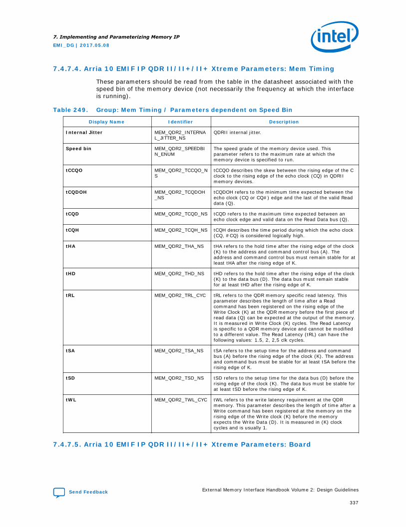
7.4.7.4. Arria 10 EMIF IP QDR II/II+/II+ Xtreme Parameters: Mem Timing
These parameters should be read from the table in the datasheet associated with thespeed bin of the memory device (not necessarily the frequency at which the interfaceis running).
Table 249. Group: Mem Timing / Parameters dependent on Speed Bin
Display Name Identifier Description
Internal Jitter MEM_QDR2_INTERNAL_JITTER_NS
QDRII internal jitter.
Speed bin MEM_QDR2_SPEEDBIN_ENUM
The speed grade of the memory device used. Thisparameter refers to the maximum rate at which thememory device is specified to run.
tCCQO MEM_QDR2_TCCQO_NS
tCCQO describes the skew between the rising edge of the Cclock to the rising edge of the echo clock (CQ) in QDRIImemory devices.
tCQDOH MEM_QDR2_TCQDOH_NS
tCQDOH refers to the minimum time expected between theecho clock (CQ or CQ#) edge and the last of the valid Readdata (Q).
tCQD MEM_QDR2_TCQD_NS tCQD refers to the maximum time expected between anecho clock edge and valid data on the Read Data bus (Q).
tCQH MEM_QDR2_TCQH_NS tCQH describes the time period during which the echo clock(CQ, #CQ) is considered logically high.
tHA MEM_QDR2_THA_NS tHA refers to the hold time after the rising edge of the clock(K) to the address and command control bus (A). Theaddress and command control bus must remain stable for atleast tHA after the rising edge of K.
tHD MEM_QDR2_THD_NS tHD refers to the hold time after the rising edge of the clock(K) to the data bus (D). The data bus must remain stablefor at least tHD after the rising edge of K.
tRL MEM_QDR2_TRL_CYC tRL refers to the QDR memory specific read latency. Thisparameter describes the length of time after a Readcommand has been registered on the rising edge of theWrite Clock (K) at the QDR memory before the first piece ofread data (Q) can be expected at the output of the memory.It is measured in Write Clock (K) cycles. The Read Latencyis specific to a QDR memory device and cannot be modifiedto a different value. The Read Latency (tRL) can have thefollowing values: 1.5, 2, 2,5 clk cycles.
tSA MEM_QDR2_TSA_NS tSA refers to the setup time for the address and commandbus (A) before the rising edge of the clock (K). The addressand command bus must be stable for at least tSA before therising edge of K.
tSD MEM_QDR2_TSD_NS tSD refers to the setup time for the data bus (D) before therising edge of the clock (K). The data bus must be stable forat least tSD before the rising edge of K.
tWL MEM_QDR2_TWL_CYC tWL refers to the write latency requirement at the QDRmemory. This parameter describes the length of time after aWrite command has been registered at the memory on therising edge of the Write clock (K) before the memoryexpects the Write Data (D). It is measured in (K) clockcycles and is usually 1.
7.4.7.5. Arria 10 EMIF IP QDR II/II+/II+ Xtreme Parameters: Board
7. Implementing and Parameterizing Memory IP
EMI_DG | 2017.05.08
Send Feedback External Memory Interface Handbook Volume 2: Design Guidelines
337
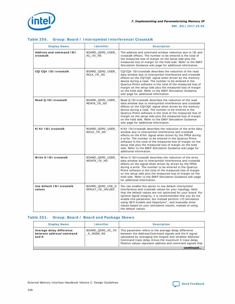
Table 250. Group: Board / Intersymbol Interference/Crosstalk
Display Name Identifier Description
Address and command ISI/crosstalk
BOARD_QDR2_USER_AC_ISI_NS
The address and command window reduction due to ISI andcrosstalk effects. The number to be entered is the total ofthe measured loss of margin on the setup side plus themeasured loss of margin on the hold side. Refer to the EMIFSimulation Guidance wiki page for additional information.
CQ/CQ# ISI/crosstalk BOARD_QDR2_USER_RCLK_ISI_NS
CQ/CQ# ISI/crosstalk describes the reduction of the readdata window due to intersymbol interference and crosstalkeffects on the CQ/CQ# signal when driven by the memorydevice during a read. The number to be entered in theQuartus Prime software is the total of the measured loss ofmargin on the setup side plus the measured loss of marginon the hold side. Refer to the EMIF Simulation Guidancewiki page for additional information.
Read Q ISI/crosstalk BOARD_QDR2_USER_RDATA_ISI_NS
Read Q ISI/crosstalk describes the reduction of the readdata window due to intersymbol interference and crosstalkeffects on the CQ/CQ# signal when driven by the memorydevice during a read. The number to be entered in theQuartus Prime software is the total of the measured loss ofmargin on the setup side plus the measured loss of marginon the hold side. Refer to the EMIF Simulation Guidancewiki page for additional information.
K/K# ISI/crosstalk BOARD_QDR2_USER_WCLK_ISI_NS
K/K# ISI/crosstalk describes the reduction of the write datawindow due to intersymbol interference and crosstalkeffects on the K/K# signal when driven by the FPGA duringa write. The number to be entered in the Quartus Primesoftware is the total of the measured loss of margin on thesetup side plus the measured loss of margin on the holdside. Refer to the EMIF Simulation Guidance wiki page foradditional information.
Write D ISI/crosstalk BOARD_QDR2_USER_WDATA_ISI_NS
Write D ISI/crosstalk describes the reduction of the writedata window due to intersymbol interference and crosstalkeffects on the signal when driven by driven by the FPGAduring a write. The number to be entered in the QuartusPrime software is the total of the measured loss of marginon the setup side plus the measured loss of margin on thehold side. Refer to the EMIF Simulation Guidance wiki pagefor additional information.
Use default ISI/crosstalkvalues
BOARD_QDR2_USE_DEFAULT_ISI_VALUES
You can enable this option to use default intersymbolinterference and crosstalk values for your topology. Notethat the default values are not optimized for your board. Foroptimal signal integrity, it is recommended that you do notenable this parameter, but instead perform I/O simulationusing IBIS models and Hyperlynx*, and manually entervalues based on your simulation results, instead of usingthe default values.
Table 251. Group: Board / Board and Package Skews
Display Name Identifier Description
Average delay differencebetween address/commandand K
BOARD_QDR2_AC_TO_K_SKEW_NS
This parameter refers to the average delay differencebetween the Address/Command signals and the K signal,calculated by averaging the longest and smallest Address/Command trace delay minus the maximum K trace delay.Positive values represent address and command signals that
continued...
7. Implementing and Parameterizing Memory IP
EMI_DG | 2017.05.08
External Memory Interface Handbook Volume 2: Design Guidelines Send Feedback
338
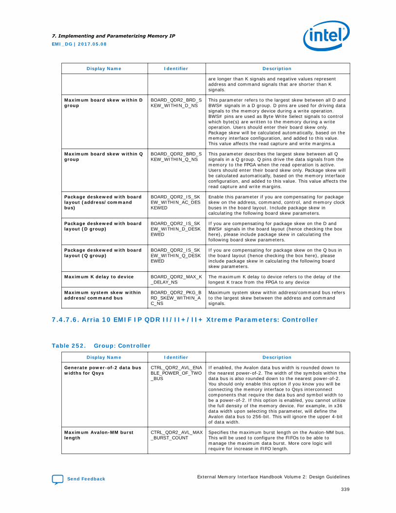
Display Name Identifier Description
are longer than K signals and negative values representaddress and command signals that are shorter than Ksignals.
Maximum board skew within Dgroup
BOARD_QDR2_BRD_SKEW_WITHIN_D_NS
This parameter refers to the largest skew between all D andBWS# signals in a D group. D pins are used for driving datasignals to the memory device during a write operation.BWS# pins are used as Byte Write Select signals to controlwhich byte(s) are written to the memory during a writeoperation. Users should enter their board skew only.Package skew will be calculated automatically, based on thememory interface configuration, and added to this value.This value affects the read capture and write margins.a
Maximum board skew within Qgroup
BOARD_QDR2_BRD_SKEW_WITHIN_Q_NS
This parameter describes the largest skew between all Qsignals in a Q group. Q pins drive the data signals from thememory to the FPGA when the read operation is active.Users should enter their board skew only. Package skew willbe calculated automatically, based on the memory interfaceconfiguration, and added to this value. This value affects theread capture and write margins.
Package deskewed with boardlayout (address/commandbus)
BOARD_QDR2_IS_SKEW_WITHIN_AC_DESKEWED
Enable this parameter if you are compensating for packageskew on the address, command, control, and memory clockbuses in the board layout. Include package skew incalculating the following board skew parameters.
Package deskewed with boardlayout (D group)
BOARD_QDR2_IS_SKEW_WITHIN_D_DESKEWED
If you are compensating for package skew on the D andBWS# signals in the board layout (hence checking the boxhere), please include package skew in calculating thefollowing board skew parameters.
Package deskewed with boardlayout (Q group)
BOARD_QDR2_IS_SKEW_WITHIN_Q_DESKEWED
If you are compensating for package skew on the Q bus inthe board layout (hence checking the box here), pleaseinclude package skew in calculating the following boardskew parameters.
Maximum K delay to device BOARD_QDR2_MAX_K_DELAY_NS
The maximum K delay to device refers to the delay of thelongest K trace from the FPGA to any device
Maximum system skew withinaddress/command bus
BOARD_QDR2_PKG_BRD_SKEW_WITHIN_AC_NS
Maximum system skew within address/command bus refersto the largest skew between the address and commandsignals.
7.4.7.6. Arria 10 EMIF IP QDR II/II+/II+ Xtreme Parameters: Controller
Table 252. Group: Controller
Display Name Identifier Description
Generate power-of-2 data buswidths for Qsys
CTRL_QDR2_AVL_ENABLE_POWER_OF_TWO_BUS
If enabled, the Avalon data bus width is rounded down tothe nearest power-of-2. The width of the symbols within thedata bus is also rounded down to the nearest power-of-2.You should only enable this option if you know you will beconnecting the memory interface to Qsys interconnectcomponents that require the data bus and symbol width tobe a power-of-2. If this option is enabled, you cannot utilizethe full density of the memory device. For example, in x36data width upon selecting this parameter, will define theAvalon data bus to 256-bit. This will ignore the upper 4-bitof data width.
Maximum Avalon-MM burstlength
CTRL_QDR2_AVL_MAX_BURST_COUNT
Specifies the maximum burst length on the Avalon-MM bus.This will be used to configure the FIFOs to be able tomanage the maximum data burst. More core logic willrequire for increase in FIFO length.
7. Implementing and Parameterizing Memory IP
EMI_DG | 2017.05.08
Send Feedback External Memory Interface Handbook Volume 2: Design Guidelines
339
7.4.7.7. Arria 10 EMIF IP QDR II/II+/II+ Xtreme Parameters: Diagnostics
Table 253. Group: Diagnostics / Simulation Options
Display Name Identifier Description
Abstract phy for fast simulation DIAG_QDR2_ABSTRACT_PHY
Specifies that the system use Abstract PHY for simulation.Abstract PHY replaces the PHY with a model for fastsimulation and can reduce simulation time by 2-3 times.Abstract PHY is available for certain protocols and devicefamilies, and only when you select Skip Calibration.
Calibration mode DIAG_SIM_CAL_MODE_ENUM
Specifies whether to skip memory interface calibrationduring simulation, or to simulate the full calibration process.Simulating the full calibration process can take hours (oreven days), depending on the width and depth of thememory interface. You can achieve much faster simulationtimes by skipping the calibration process, but that is onlyexpected to work when the memory model is ideal and theinterconnect delays are zero. If you enable this parameter,the interface still performs some memory initializationbefore starting normal operations. Abstract PHY issupported with skip calibration.
Table 254. Group: Diagnostics / Calibration Debug Options
Display Name Identifier Description
Enable Daisy-Chaining forQuartus Prime EMIF DebugToolkit/On-Chip Debug Port
DIAG_EXPORT_SEQ_AVALON_MASTER
Specifies that the IP export an Avalon-MM master interface(cal_debug_out) which can connect to the cal_debuginterface of other EMIF cores residing in the same I/Ocolumn. This parameter applies only if the EMIF DebugToolkit or On-Chip Debug Port is enabled. Refer to theDebugging Multiple EMIFs wiki page for more informationabout debugging multiple EMIFs.
Quartus Prime EMIF DebugToolkit/On-Chip Debug Port
DIAG_EXPORT_SEQ_AVALON_SLAVE
Specifies the connectivity of an Avalon slave interface foruse by the Quartus Prime EMIF Debug Toolkit or user corelogic. If you set this parameter to "Disabled," no debugfeatures are enabled. If you set this parameter to "Export,"an Avalon slave interface named "cal_debug" is exportedfrom the IP. To use this interface with the EMIF DebugToolkit, you must instantiate and connect an EMIF debuginterface IP core to it, or connect it to the cal_debug_outinterface of another EMIF core. If you select "Add EMIFDebug Interface", an EMIF debug interface componentcontaining a JTAG Avalon Master is connected to the debugport, allowing the core to be accessed by the EMIF DebugToolkit. Only one EMIF debug interface should beinstantiated per I/O column. You can chain additional EMIFor PHYLite cores to the first by enabling the "Enable Daisy-Chaining for Quartus Prime EMIF Debug Toolkit/On-ChipDebug Port" option for all cores in the chain, and selecting"Export" for the "Quartus Prime EMIF Debug Toolkit/On-ChipDebug Port" option on all cores after the first.
Interface ID DIAG_INTERFACE_ID Identifies interfaces within the I/O column, for use by theEMIF Debug Toolkit and the On-Chip Debug Port. InterfaceIDs should be unique among EMIF cores within the sameI/O column. If the Quartus Prime EMIF Debug Toolkit/On-Chip Debug Port parameter is set to Disabled, the interfaceID is unused.
Use Soft NIOS Processor forOn-Chip Debug
DIAG_SOFT_NIOS_MODE
Enables a soft Nios processor as a peripheral component toaccess the On-Chip Debug Port. Only one interface in acolumn can activate this option.
7. Implementing and Parameterizing Memory IP
EMI_DG | 2017.05.08
External Memory Interface Handbook Volume 2: Design Guidelines Send Feedback
340

Table 255. Group: Diagnostics / Example Design
Display Name Identifier Description
Enable In-System-Sources-and-Probes
DIAG_EX_DESIGN_ISSP_EN
Enables In-System-Sources-and-Probes in the exampledesign for common debug signals, such as calibration statusor example traffic generator per-bit status. This parametermust be enabled if you want to do driver margining.
Number of core clocks sharingslaves to instantiate in theexample design
DIAG_EX_DESIGN_NUM_OF_SLAVES
Specifies the number of core clock sharing slaves toinstantiate in the example design. This parameter appliesonly if you set the "Core clocks sharing" parameter in the"General" tab to Master or Slave.
Table 256. Group: Diagnostics / Traffic Generator
Display Name Identifier Description
Bypass the default trafficpattern
DIAG_BYPASS_DEFAULT_PATTERN
Specifies that the controller/interface bypass the trafficgenerator 2.0 default pattern after reset. If you do notenable this parameter, the traffic generator does not asserta pass or fail status until the generator is configured andsignaled to start by its Avalon configuration interface.
Bypass the traffic generatorrepeated-writes/repeated-reads test pattern
DIAG_BYPASS_REPEAT_STAGE
Specifies that the controller/interface bypass the trafficgenerator's repeat test stage. If you do not enable thisparameter, every write and read is repeated several times.
Bypass the traffic generatorstress pattern
DIAG_BYPASS_STRESS_STAGE
Specifies that the controller/interface bypass the trafficgenerator's stress pattern stage. (Stress patterns are meantto create worst-case signal integrity patterns on the datapins.) If you do not enable this parameter, the trafficgenerator does not assert a pass or fail status until thegenerator is configured and signaled to start by its Avalonconfiguration interface.
Bypass the user-configuredtraffic stage
DIAG_BYPASS_USER_STAGE
Specifies that the controller/interface bypass the user-configured traffic generator's pattern after reset. If you donot enable this parameter, the traffic generator does notassert a pass or fail status until the generator is configuredand signaled to start by its Avalon configuration interface.Configuration can be done by connecting to the trafficgenerator via the EMIF Debug Toolkit, or by using customlogic connected to the Avalon-MM configuration slave porton the traffic generator. Configuration can also be simulatedusing the example testbench provided in thealtera_emif_avl_tg_2_tb.sv file.
Run diagnostic on infinite testduration
DIAG_INFI_TG2_ERR_TEST
Specifies that the traffic generator run indefinitely until thefirst error is detected.
Export Traffic Generator 2.0configuration interface
DIAG_TG_AVL_2_EXPORT_CFG_INTERFACE
Specifies that the IP export an Avalon-MM slave port forconfiguring the Traffic Generator. This is required only if youare configuring the traffic generator through user logic andnot through through the EMIF Debug Toolkit.
Use configurable Avalon trafficgenerator 2.0
DIAG_USE_TG_AVL_2 This option allows users to add the new configurable Avalontraffic generator to the example design.
Table 257. Group: Diagnostics / Performance
Display Name Identifier Description
Enable Efficiency Monitor DIAG_EFFICIENCY_MONITOR
Adds an Efficiency Monitor component to the Avalon-MMinterface of the memory controller, allowing you to viewefficiency statistics of the interface. You can access theefficiency statistics using the EMIF Debug Toolkit.
7. Implementing and Parameterizing Memory IP
EMI_DG | 2017.05.08
Send Feedback External Memory Interface Handbook Volume 2: Design Guidelines
341
Table 258. Group: Diagnostics / Miscellaneous
Display Name Identifier Description
Use short Qsys interface names SHORT_QSYS_INTERFACE_NAMES
Specifies the use of short interface names, for improvedusability and consistency with other Qsys components. Ifthis parameter is disabled, the names of Qsys interfacesexposed by the IP will include the type and direction of theinterface. Long interface names are supported forbackward-compatibility and will be removed in a futurerelease.
7.4.7.8. Arria 10 EMIF IP QDR II/II+/II+ Xtreme Parameters: Example Designs
Table 259. Group: Example Designs / Available Example Designs
Display Name Identifier Description
Select design EX_DESIGN_GUI_QDR2_SEL_DESIGN
Specifies the creation of a full Quartus Prime project,instantiating an external memory interface and an exampletraffic generator, according to your parameterization. Afterthe design is created, you can specify the target device andpin location assignments, run a full compilation, verifytiming closure, and test the interface on your board usingthe programming file created by the Quartus Primeassembler. The 'Generate Example Design' button lets yougenerate simulation or synthesis file sets.
Table 260. Group: Example Designs / Example Design Files
Display Name Identifier Description
Simulation EX_DESIGN_GUI_QDR2_GEN_SIM
Specifies that the 'Generate Example Design' button createall necessary file sets for simulation. Expect a shortadditional delay as the file set is created. If you do notenable this parameter, simulation file sets are not created.Instead, the output directory will contain the ed_sim.qsysfile which holds Qsys details of the simulation exampledesign, and a make_sim_design.tcl file with othercorresponding tcl files. You can run make_sim_design.tclfrom a command line to generate the simulation exampledesign. The generated example designs for varioussimulators are stored in the /sim sub-directory.
Synthesis EX_DESIGN_GUI_QDR2_GEN_SYNTH
Specifies that the 'Generate Example Design' button createall necessary file sets for synthesis. Expect a shortadditional delay as the file set is created. If you do notenable this parameter, synthesis file sets are not created.Instead, the output directory will contain the ed_synth.qsysfile which holds Qsys details of the synthesis exampledesign, and a make_qii_design.tcl script with othercorresponding tcl files. You can run make_qii_design.tclfrom a command line to generate the synthesis exampledesign. The generated example design is stored in the /qiisub-directory.
Table 261. Group: Example Designs / Generated HDL Format
Display Name Identifier Description
Simulation HDL format EX_DESIGN_GUI_QDR2_HDL_FORMAT
This option lets you choose the format of HDL in whichgenerated simulation files are created.
7. Implementing and Parameterizing Memory IP
EMI_DG | 2017.05.08
External Memory Interface Handbook Volume 2: Design Guidelines Send Feedback
342
Table 262. Group: Example Designs / Target Development Kit
Display Name Identifier Description
Select board EX_DESIGN_GUI_QDR2_TARGET_DEV_KIT
Specifies that when you select a development kit with amemory module, the generated example design contains allsettings and fixed pin assignments to run on the selectedboard. You must select a development kit preset togenerate a working example design for the specifieddevelopment kit. Any IP settings not applied directly from adevelopment kit preset will not have guaranteed resultswhen testing the development kit. To exclude hardwaresupport of the example design, select 'none' from the'Select board' pull down menu. When you apply adevelopment kit preset, all IP parameters are automaticallyset appropriately to match the selected preset. If you wantto save your current settings, you should do so before youapply the preset. You can save your settings under adifferent name using File->Save as.
7.4.7.9. About Memory Presets
Presets help simplify the process of copying memory parameter values from memorydevice data sheets to the EMIF parameter editor.
For DDRx protocols, the memory presets are named using the following convention:
PROTOCOL-SPEEDBIN LATENCY FORMAT-AND-TOPOLOGY CAPACITY (INTERNAL-ORGANIZATION)
For example, the preset named DDR4-2666U CL18 Component 1CS 2Gb (512Mbx 4) refers to a DDR4 x4 component rated at the DDR4-2666U JEDEC speed bin, withnominal CAS latency of 18 cycles, one chip-select, and a total memory space of 2Gb.The JEDEC memory specification defines multiple speed bins for a given frequency(that is, DDR4-2666U and DDR4-2666V). You may be able to determine the exactspeed bin implemented by your memory device using its nominal latency. When indoubt, contact your memory vendor.
For RLDRAMx and QDRx protocols, the memory presets are named based on thevendor's device part number.
When the preset list does not contain the exact configuration required, you can stillminimize data entry by selecting the preset closest to your configuration and thenmodify parameters as required.
Prior to production you should always review the parameter values to ensure that theymatch your memory device data sheet, regardless of whether a preset is used or not.Incorrect memory parameters can cause functional failures.
7.4.8. Arria 10 EMIF IP RLDRAM 3 Parameters
The Arria 10 EMIF IP parameter editor allows you to parameterize settings for theArria 10 EMIF IP.
The text window at the bottom of the parameter editor displays information about thememory interface, as well as warning and error messages. You should correct anyerrors indicated in this window before clicking the Finish button.
Note: Default settings are the minimum required to achieve timing, and may vary dependingon memory protocol.
7. Implementing and Parameterizing Memory IP
EMI_DG | 2017.05.08
Send Feedback External Memory Interface Handbook Volume 2: Design Guidelines
343
The following tables describe the parameterization settings available in the parametereditor for the Arria 10 EMIF IP.
7.4.8.1. Arria 10 EMIF IP RLDRAM 3 Parameters: General
Table 263. Group: General / FPGA
Display Name Identifier Description
Speed grade PHY_FPGA_SPEEDGRADE_GUI
Indicates the device speed grade, and whether it is anengineering sample (ES) or production device. This value isbased on the device that you select in the parameter editor.If you do not specify a device, the system assumes adefault value. Ensure that you always specify the correctdevice during IP generation, otherwise your IP may notwork in hardware.
Table 264. Group: General / Interface
Display Name Identifier Description
Configuration PHY_CONFIG_ENUM Specifies the configuration of the memory interface. Theavailable options depend on the protocol in use. Optionsinclude Hard PHY and Hard Controller, Hard PHY and SoftController, or Hard PHY only. If you select Hard PHY only,the AFI interface is exported to allow connection of acustom memory controller or third-party IP.
Instantiate two controllerssharing a Ping Pong PHY
PHY_PING_PONG_EN Specifies the instantiation of two identical memorycontrollers that share an address/command bus through theuse of Ping Pong PHY. This parameter is available only if youspecify the Hard PHY and Hard Controller option. When thisparameter is enabled, the IP exposes two independentAvalon interfaces to the user logic, and a single externalmemory interface with double width for the data bus andthe CS#, CKE, ODT, and CK/CK# signals.
Table 265. Group: General / Clocks
Display Name Identifier Description
Core clocks sharing PHY_CORE_CLKS_SHARING_ENUM
When a design contains multiple interfaces of the sameprotocol, rate, frequency, and PLL reference clock source,they can share a common set of core clock domains. Bysharing core clock domains, they reduce clock networkusage and avoid clock synchronization logic between theinterfaces. To share core clocks, denote one of theinterfaces as "Master", and the remaining interfaces as"Slave". In the RTL, connect the clks_sharing_master_outsignal from the master interface to theclks_sharing_slave_in signal of all the slave interfaces. Bothmaster and slave interfaces still expose their own outputclock ports in the RTL (for example, emif_usr_clk, afi_clk),but the physical signals are equivalent, hence it does notmatter whether a clock port from a master or a slave isused. As the combined width of all interfaces sharing thesame core clock increases, you may encounter timingclosure difficulty for transfers between the FPGA core andthe periphery.
Memory clock frequency PHY_MEM_CLK_FREQ_MHZ
Specifies the operating frequency of the memory interfacein MHz. If you change the memory frequency, you shouldupdate the memory latency parameters on the "Memory"tab and the memory timing parameters on the "MemTiming" tab.
continued...
7. Implementing and Parameterizing Memory IP
EMI_DG | 2017.05.08
External Memory Interface Handbook Volume 2: Design Guidelines Send Feedback
344
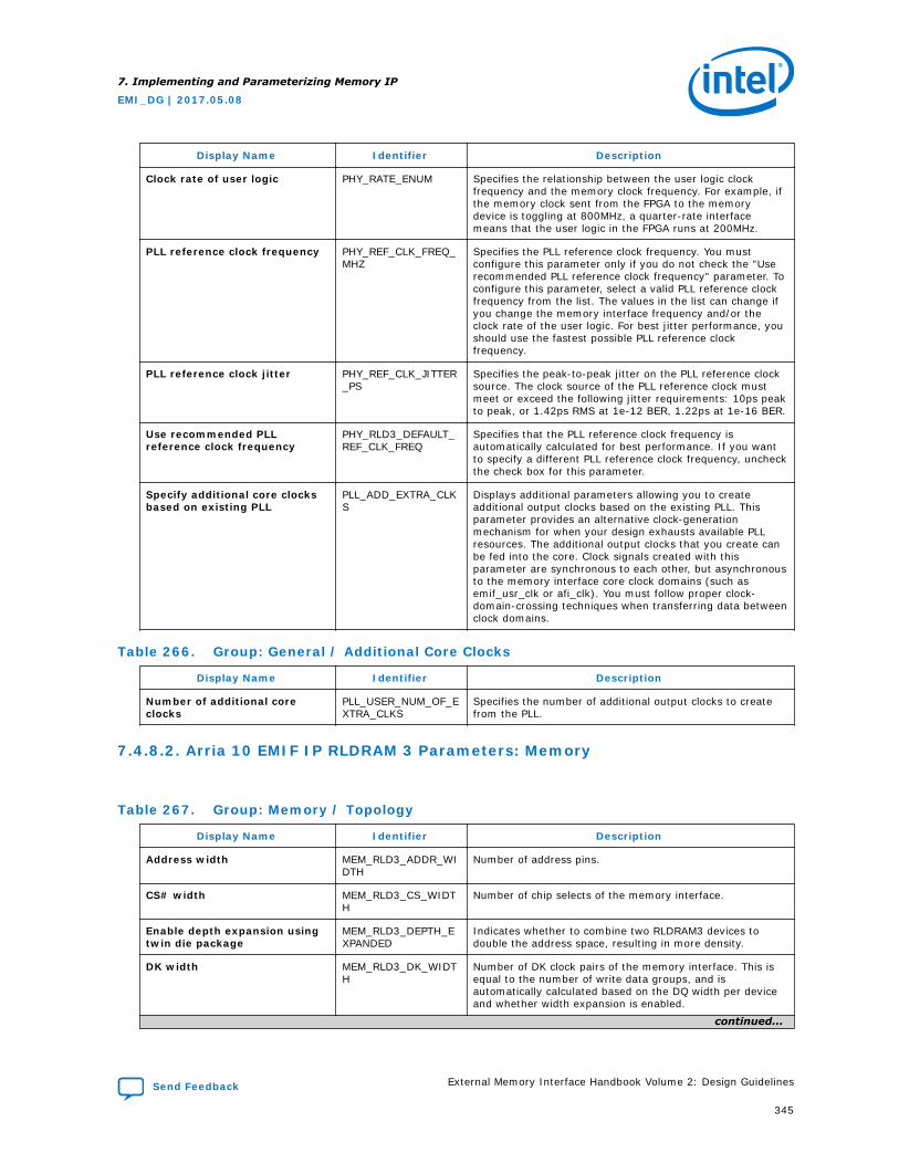
Display Name Identifier Description
Clock rate of user logic PHY_RATE_ENUM Specifies the relationship between the user logic clockfrequency and the memory clock frequency. For example, ifthe memory clock sent from the FPGA to the memorydevice is toggling at 800MHz, a quarter-rate interfacemeans that the user logic in the FPGA runs at 200MHz.
PLL reference clock frequency PHY_REF_CLK_FREQ_MHZ
Specifies the PLL reference clock frequency. You mustconfigure this parameter only if you do not check the "Userecommended PLL reference clock frequency" parameter. Toconfigure this parameter, select a valid PLL reference clockfrequency from the list. The values in the list can change ifyou change the memory interface frequency and/or theclock rate of the user logic. For best jitter performance, youshould use the fastest possible PLL reference clockfrequency.
PLL reference clock jitter PHY_REF_CLK_JITTER_PS
Specifies the peak-to-peak jitter on the PLL reference clocksource. The clock source of the PLL reference clock mustmeet or exceed the following jitter requirements: 10ps peakto peak, or 1.42ps RMS at 1e-12 BER, 1.22ps at 1e-16 BER.
Use recommended PLLreference clock frequency
PHY_RLD3_DEFAULT_REF_CLK_FREQ
Specifies that the PLL reference clock frequency isautomatically calculated for best performance. If you wantto specify a different PLL reference clock frequency, uncheckthe check box for this parameter.
Specify additional core clocksbased on existing PLL
PLL_ADD_EXTRA_CLKS
Displays additional parameters allowing you to createadditional output clocks based on the existing PLL. Thisparameter provides an alternative clock-generationmechanism for when your design exhausts available PLLresources. The additional output clocks that you create canbe fed into the core. Clock signals created with thisparameter are synchronous to each other, but asynchronousto the memory interface core clock domains (such asemif_usr_clk or afi_clk). You must follow proper clock-domain-crossing techniques when transferring data betweenclock domains.
Table 266. Group: General / Additional Core Clocks
Display Name Identifier Description
Number of additional coreclocks
PLL_USER_NUM_OF_EXTRA_CLKS
Specifies the number of additional output clocks to createfrom the PLL.
7.4.8.2. Arria 10 EMIF IP RLDRAM 3 Parameters: Memory
Table 267. Group: Memory / Topology
Display Name Identifier Description
Address width MEM_RLD3_ADDR_WIDTH
Number of address pins.
CS# width MEM_RLD3_CS_WIDTH
Number of chip selects of the memory interface.
Enable depth expansion usingtwin die package
MEM_RLD3_DEPTH_EXPANDED
Indicates whether to combine two RLDRAM3 devices todouble the address space, resulting in more density.
DK width MEM_RLD3_DK_WIDTH
Number of DK clock pairs of the memory interface. This isequal to the number of write data groups, and isautomatically calculated based on the DQ width per deviceand whether width expansion is enabled.
continued...
7. Implementing and Parameterizing Memory IP
EMI_DG | 2017.05.08
Send Feedback External Memory Interface Handbook Volume 2: Design Guidelines
345
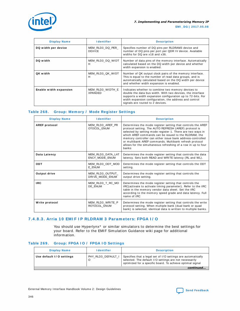
Display Name Identifier Description
DQ width per device MEM_RLD3_DQ_PER_DEVICE
Specifies number of DQ pins per RLDRAM3 device andnumber of DQ pins per port per QDR IV device. Availablewidths for DQ are x18 and x36.
DQ width MEM_RLD3_DQ_WIDTH
Number of data pins of the memory interface. Automaticallycalculated based on the DQ width per device and whetherwidth expansion is enabled.
QK width MEM_RLD3_QK_WIDTH
Number of QK output clock pairs of the memory interface.This is equal to the number of read data groups, and isautomatically calculated based on the DQ width per deviceand whether width expansion is enabled.
Enable width expansion MEM_RLD3_WIDTH_EXPANDED
Indicates whether to combine two memory devices todouble the data bus width. With two devices, the interfacesupports a width expansion configuration up to 72-bits. Forwidth expansion configuration, the address and controlsignals are routed to 2 devices.
Table 268. Group: Memory / Mode Register Settings
Display Name Identifier Description
AREF protocol MEM_RLD3_AREF_PROTOCOL_ENUM
Determines the mode register setting that controls the AREFprotocol setting. The AUTO REFRESH (AREF) protocol isselected by setting mode register 1. There are two ways inwhich AREF commands can be issued to the RLDRAM, thememory controller can either issue bank address-controlledor multibank AREF commands. Multibank refresh protocolallows for the simultaneous refreshing of a row in up to fourbanks
Data Latency MEM_RLD3_DATA_LATENCY_MODE_ENUM
Determines the mode register setting that controls the datalatency. Sets both READ and WRITE latency (RL and WL).
ODT MEM_RLD3_ODT_MODE_ENUM
Determines the mode register setting that controls the ODTsetting.
Output drive MEM_RLD3_OUTPUT_DRIVE_MODE_ENUM
Determines the mode register setting that controls theoutput drive setting.
tRC MEM_RLD3_T_RC_MODE_ENUM
Determines the mode register setting that controls thetRC(activate to activate timing parameter). Refer to the tRCtable in the memory vendor data sheet. Set the tRCaccording to the memory speed grade and data latency. Fullname of tRC
Write protocol MEM_RLD3_WRITE_PROTOCOL_ENUM
Determines the mode register setting that controls the writeprotocol setting. When multiple bank (dual bank or quadbank) is selected, identical data is written to multiple banks.
7.4.8.3. Arria 10 EMIF IP RLDRAM 3 Parameters: FPGA I/O
You should use Hyperlynx* or similar simulators to determine the best settings foryour board. Refer to the EMIF Simulation Guidance wiki page for additionalinformation.
Table 269. Group: FPGA IO / FPGA IO Settings
Display Name Identifier Description
Use default I/O settings PHY_RLD3_DEFAULT_IO
Specifies that a legal set of I/O settings are automaticallyselected. The default I/O settings are not necessarilyoptimized for a specific board. To achieve optimal signal
continued...
7. Implementing and Parameterizing Memory IP
EMI_DG | 2017.05.08
External Memory Interface Handbook Volume 2: Design Guidelines Send Feedback
346

Display Name Identifier Description
integrity, perform I/O simulations with IBIS models andenter the I/O settings manually, based on simulationresults.
Voltage PHY_RLD3_IO_VOLTAGE
The voltage level for the I/O pins driving the signalsbetween the memory device and the FPGA memoryinterface.
Periodic OCT re-calibration PHY_USER_PERIODIC_OCT_RECAL_ENUM
Specifies that the system periodically recalibrate on-chiptermination (OCT) to minimize variations in terminationvalue caused by changing operating conditions (such aschanges in temperature). By recalibrating OCT, I/O timingmargins are improved. When enabled, this parametercauses the PHY to halt user traffic about every 0.5 secondsfor about 1900 memory clock cycles, to perform OCTrecalibration. Efficiency is reduced by about 1% when thisoption is enabled.
Table 270. Group: FPGA IO / Address/Command
Display Name Identifier Description
I/O standard PHY_RLD3_USER_AC_IO_STD_ENUM
Specifies the I/O electrical standard for the address/command pins of the memory interface. The selected I/Ostandard configures the circuit within the I/O buffer tomatch the industry standard.
Output mode PHY_RLD3_USER_AC_MODE_ENUM
This parameter allows you to change the current drivestrength or termination settings for the selected I/Ostandard. Perform board simulation with IBIS models todetermine the best settings for your design.
Slew rate PHY_RLD3_USER_AC_SLEW_RATE_ENUM
Specifies the slew rate of the address/command outputpins. The slew rate (or edge rate) describes how quickly thesignal can transition, measured in voltage per unit time.Perform board simulations to determine the slew rate thatprovides the best eye opening for the address andcommand signals.
Table 271. Group: FPGA IO / Memory Clock
Display Name Identifier Description
I/O standard PHY_RLD3_USER_CK_IO_STD_ENUM
Specifies the I/O electrical standard for the memory clockpins. The selected I/O standard configures the circuit withinthe I/O buffer to match the industry standard.
Output mode PHY_RLD3_USER_CK_MODE_ENUM
This parameter allows you to change the current drivestrength or termination settings for the selected I/Ostandard. Perform board simulation with IBIS models todetermine the best settings for your design.
Slew rate PHY_RLD3_USER_CK_SLEW_RATE_ENUM
Specifies the slew rate of the address/command outputpins. The slew rate (or edge rate) describes how quickly thesignal can transition, measured in voltage per unit time.Perform board simulations to determine the slew rate thatprovides the best eye opening for the address andcommand signals.
7. Implementing and Parameterizing Memory IP
EMI_DG | 2017.05.08
Send Feedback External Memory Interface Handbook Volume 2: Design Guidelines
347
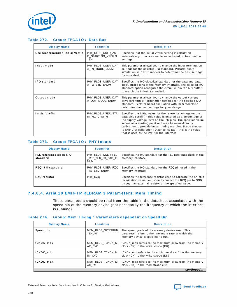
Table 272. Group: FPGA IO / Data Bus
Display Name Identifier Description
Use recommended initial Vrefin PHY_RLD3_USER_AUTO_STARTING_VREFIN_EN
Specifies that the initial Vrefin setting is calculatedautomatically, to a reasonable value based on terminationsettings.
Input mode PHY_RLD3_USER_DATA_IN_MODE_ENUM
This parameter allows you to change the input terminationsettings for the selected I/O standard. Perform boardsimulation with IBIS models to determine the best settingsfor your design.
I/O standard PHY_RLD3_USER_DATA_IO_STD_ENUM
Specifies the I/O electrical standard for the data and dataclock/strobe pins of the memory interface. The selected I/Ostandard option configures the circuit within the I/O bufferto match the industry standard.
Output mode PHY_RLD3_USER_DATA_OUT_MODE_ENUM
This parameter allows you to change the output currentdrive strength or termination settings for the selected I/Ostandard. Perform board simulation with IBIS models todetermine the best settings for your design.
Initial Vrefin PHY_RLD3_USER_STARTING_VREFIN
Specifies the initial value for the reference voltage on thedata pins (Vrefin). This value is entered as a percentage ofthe supply voltage level on the I/O pins. The specified valueserves as a starting point and may be overridden bycalibration to provide better timing margins. If you chooseto skip Vref calibration (Diagnostics tab), this is the valuethat is used as the Vref for the interface.
Table 273. Group: FPGA IO / PHY Inputs
Display Name Identifier Description
PLL reference clock I/Ostandard
PHY_RLD3_USER_PLL_REF_CLK_IO_STD_ENUM
Specifies the I/O standard for the PLL reference clock of thememory interface.
RZQ I/O standard PHY_RLD3_USER_RZQ_IO_STD_ENUM
Specifies the I/O standard for the RZQ pin used in thememory interface.
RZQ resistor PHY_RZQ Specifies the reference resistor used to calibrate the on-chiptermination value. You should connect the RZQ pin to GNDthrough an external resistor of the specified value.
7.4.8.4. Arria 10 EMIF IP RLDRAM 3 Parameters: Mem Timing
These parameters should be read from the table in the datasheet associated with thespeed bin of the memory device (not necessarily the frequency at which the interfaceis running).
Table 274. Group: Mem Timing / Parameters dependent on Speed Bin
Display Name Identifier Description
Speed bin MEM_RLD3_SPEEDBIN_ENUM
The speed grade of the memory device used. Thisparameter refers to the maximum rate at which thememory device is specified to run.
tCKDK_max MEM_RLD3_TCKDK_MAX_CYC
tCKDK_max refers to the maximum skew from the memoryclock (CK) to the write strobe (DK).
tCKDK_min MEM_RLD3_TCKDK_MIN_CYC
tCKDK_min refers to the minimum skew from the memoryclock (CK) to the write strobe (DK).
tCKQK_max MEM_RLD3_TCKQK_MAX_PS
tCKQK_max refers to the maximum skew from the memoryclock (CK) to the read strobe (QK).
continued...
7. Implementing and Parameterizing Memory IP
EMI_DG | 2017.05.08
External Memory Interface Handbook Volume 2: Design Guidelines Send Feedback
348
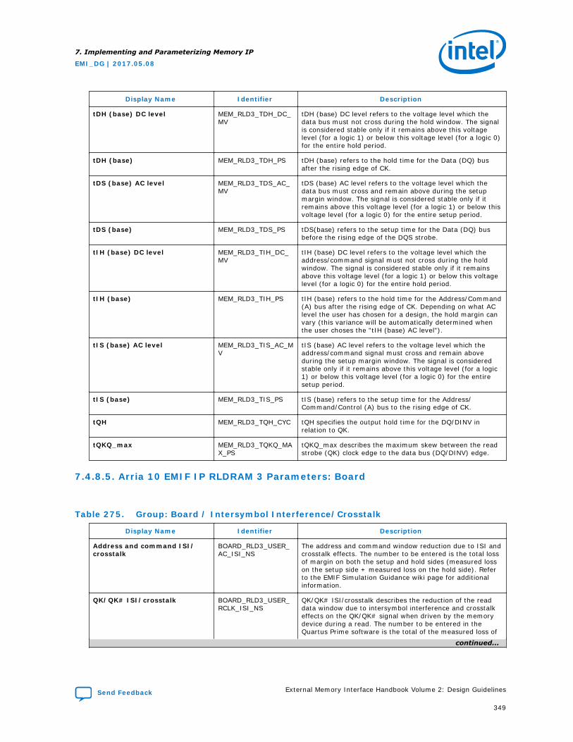
Display Name Identifier Description
tDH (base) DC level MEM_RLD3_TDH_DC_MV
tDH (base) DC level refers to the voltage level which thedata bus must not cross during the hold window. The signalis considered stable only if it remains above this voltagelevel (for a logic 1) or below this voltage level (for a logic 0)for the entire hold period.
tDH (base) MEM_RLD3_TDH_PS tDH (base) refers to the hold time for the Data (DQ) busafter the rising edge of CK.
tDS (base) AC level MEM_RLD3_TDS_AC_MV
tDS (base) AC level refers to the voltage level which thedata bus must cross and remain above during the setupmargin window. The signal is considered stable only if itremains above this voltage level (for a logic 1) or below thisvoltage level (for a logic 0) for the entire setup period.
tDS (base) MEM_RLD3_TDS_PS tDS(base) refers to the setup time for the Data (DQ) busbefore the rising edge of the DQS strobe.
tIH (base) DC level MEM_RLD3_TIH_DC_MV
tIH (base) DC level refers to the voltage level which theaddress/command signal must not cross during the holdwindow. The signal is considered stable only if it remainsabove this voltage level (for a logic 1) or below this voltagelevel (for a logic 0) for the entire hold period.
tIH (base) MEM_RLD3_TIH_PS tIH (base) refers to the hold time for the Address/Command(A) bus after the rising edge of CK. Depending on what AClevel the user has chosen for a design, the hold margin canvary (this variance will be automatically determined whenthe user choses the "tIH (base) AC level").
tIS (base) AC level MEM_RLD3_TIS_AC_MV
tIS (base) AC level refers to the voltage level which theaddress/command signal must cross and remain aboveduring the setup margin window. The signal is consideredstable only if it remains above this voltage level (for a logic1) or below this voltage level (for a logic 0) for the entiresetup period.
tIS (base) MEM_RLD3_TIS_PS tIS (base) refers to the setup time for the Address/Command/Control (A) bus to the rising edge of CK.
tQH MEM_RLD3_TQH_CYC tQH specifies the output hold time for the DQ/DINV inrelation to QK.
tQKQ_max MEM_RLD3_TQKQ_MAX_PS
tQKQ_max describes the maximum skew between the readstrobe (QK) clock edge to the data bus (DQ/DINV) edge.
7.4.8.5. Arria 10 EMIF IP RLDRAM 3 Parameters: Board
Table 275. Group: Board / Intersymbol Interference/Crosstalk
Display Name Identifier Description
Address and command ISI/crosstalk
BOARD_RLD3_USER_AC_ISI_NS
The address and command window reduction due to ISI andcrosstalk effects. The number to be entered is the total lossof margin on both the setup and hold sides (measured losson the setup side + measured loss on the hold side). Referto the EMIF Simulation Guidance wiki page for additionalinformation.
QK/QK# ISI/crosstalk BOARD_RLD3_USER_RCLK_ISI_NS
QK/QK# ISI/crosstalk describes the reduction of the readdata window due to intersymbol interference and crosstalkeffects on the QK/QK# signal when driven by the memorydevice during a read. The number to be entered in theQuartus Prime software is the total of the measured loss of
continued...
7. Implementing and Parameterizing Memory IP
EMI_DG | 2017.05.08
Send Feedback External Memory Interface Handbook Volume 2: Design Guidelines
349

Display Name Identifier Description
margin on the setup side plus the measured loss of marginon the hold side. Refer to the EMIF Simulation Guidancewiki page for additional information.
DK/DK# ISI/crosstalk BOARD_RLD3_USER_WCLK_ISI_NS
DK/DK# ISI/crosstalk describes the reduction of the writedata window due to intersymbol interference and crosstalkeffects on the DK/DK# signal when driven by the FPGAduring a write. The number to be entered in the QuartusPrime software is the total of the measured loss of marginon the setup side plus the measured loss of margin on thehold side. Refer to the EMIF Simulation Guidance wiki pagefor additional information.
Write DQ ISI/crosstalk BOARD_RLD3_USER_WDATA_ISI_NS
The reduction of the write data window due to ISI andcrosstalk effects on the DQ signal when driven by the FPGAduring a write. The number to be entered is the total of themeasured loss of margin on the setup side plus themeasured loss of margin on the hold side. Refer to the EMIFSimulation Guidance wiki page for additional information.
Use default ISI/crosstalkvalues
BOARD_RLD3_USE_DEFAULT_ISI_VALUES
You can enable this option to use default intersymbolinterference and crosstalk values for your topology. Notethat the default values are not optimized for your board. Foroptimal signal integrity, it is recommended that you do notenable this parameter, but instead perform I/O simulationusing IBIS models and Hyperlynx*, and manually entervalues based on your simulation results, instead of usingthe default values.
Table 276. Group: Board / Board and Package Skews
Display Name Identifier Description
Average delay differencebetween address/commandand CK
BOARD_RLD3_AC_TO_CK_SKEW_NS
The average delay difference between the address/command signals and the CK signal, calculated by averagingthe longest and smallest address/command signal tracedelay minus the maximum CK trace delay. Positive valuesrepresent address and command signals that are longerthan CK signals and negative values represent address andcommand signals that are shorter than CK signals.
Maximum board skew withinQK group
BOARD_RLD3_BRD_SKEW_WITHIN_QK_NS
Maximum board skew within QK group refers to the largestskew between all DQ and DM pins in a QK group. This valuecan affect the read capture and write margins.
Average delay differencebetween DK and CK
BOARD_RLD3_DK_TO_CK_SKEW_NS
This parameter describes the average delay differencebetween the DK signals and the CK signal, calculated byaveraging the longest and smallest DK trace delay minusthe CK trace delay. Positive values represent DK signals thatare longer than CK signals and negative values representDK signals that are shorter than CK signals.
Package deskewed with boardlayout (address/commandbus)
BOARD_RLD3_IS_SKEW_WITHIN_AC_DESKEWED
Enable this parameter if you are compensating for packageskew on the address, command, control, and memory clockbuses in the board layout. Include package skew incalculating the following board skew parameters.
Package deskewed with boardlayout (QK group)
BOARD_RLD3_IS_SKEW_WITHIN_QK_DESKEWED
If you are compensating for package skew on the QK bus inthe board layout (hence checking the box here), pleaseinclude package skew in calculating the following boardskew parameters.
Maximum CK delay to device BOARD_RLD3_MAX_CK_DELAY_NS
The maximum CK delay to device refers to the delay of thelongest CK trace from the FPGA to any device.
Maximum DK delay to device BOARD_RLD3_MAX_DK_DELAY_NS
The maximum DK delay to device refers to the delay of thelongest DK trace from the FPGA to any device.
continued...
7. Implementing and Parameterizing Memory IP
EMI_DG | 2017.05.08
External Memory Interface Handbook Volume 2: Design Guidelines Send Feedback
350
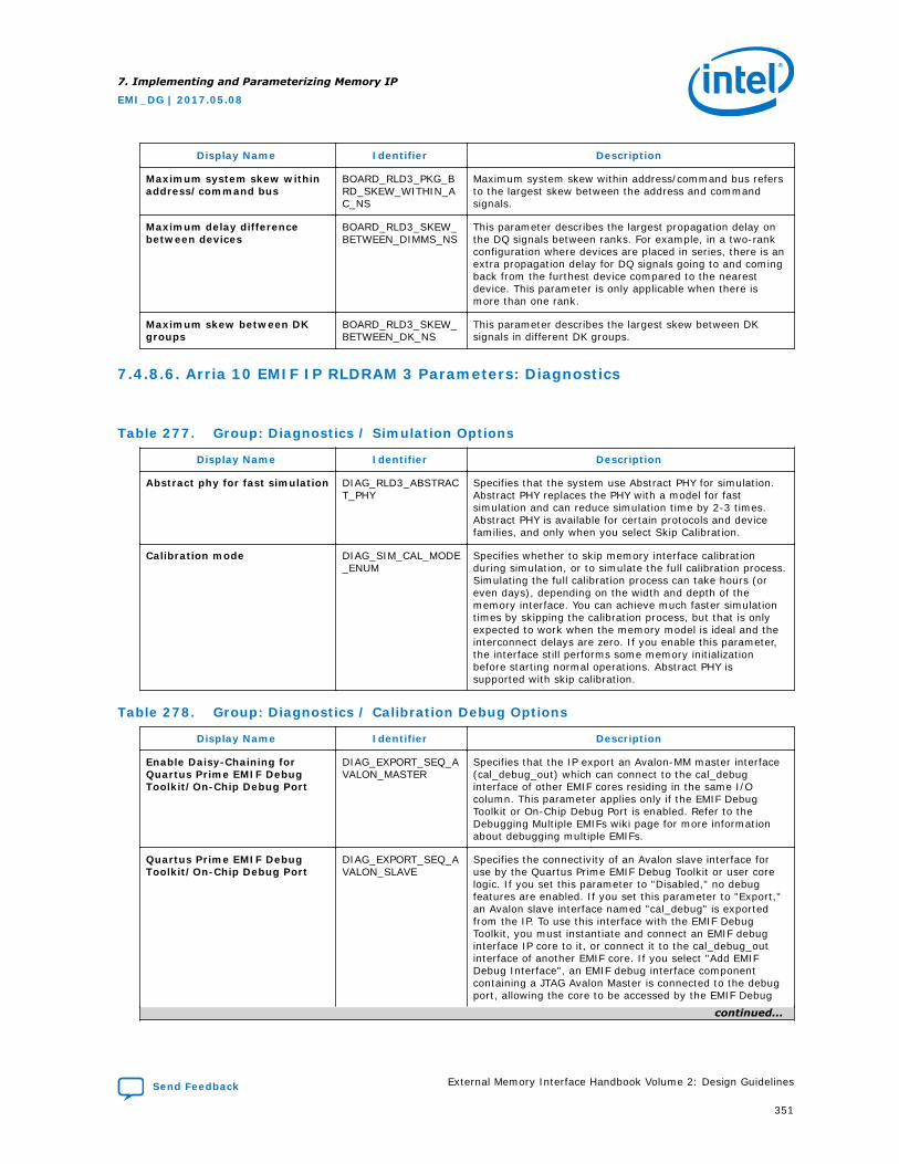
Display Name Identifier Description
Maximum system skew withinaddress/command bus
BOARD_RLD3_PKG_BRD_SKEW_WITHIN_AC_NS
Maximum system skew within address/command bus refersto the largest skew between the address and commandsignals.
Maximum delay differencebetween devices
BOARD_RLD3_SKEW_BETWEEN_DIMMS_NS
This parameter describes the largest propagation delay onthe DQ signals between ranks. For example, in a two-rankconfiguration where devices are placed in series, there is anextra propagation delay for DQ signals going to and comingback from the furthest device compared to the nearestdevice. This parameter is only applicable when there ismore than one rank.
Maximum skew between DKgroups
BOARD_RLD3_SKEW_BETWEEN_DK_NS
This parameter describes the largest skew between DKsignals in different DK groups.
7.4.8.6. Arria 10 EMIF IP RLDRAM 3 Parameters: Diagnostics
Table 277. Group: Diagnostics / Simulation Options
Display Name Identifier Description
Abstract phy for fast simulation DIAG_RLD3_ABSTRACT_PHY
Specifies that the system use Abstract PHY for simulation.Abstract PHY replaces the PHY with a model for fastsimulation and can reduce simulation time by 2-3 times.Abstract PHY is available for certain protocols and devicefamilies, and only when you select Skip Calibration.
Calibration mode DIAG_SIM_CAL_MODE_ENUM
Specifies whether to skip memory interface calibrationduring simulation, or to simulate the full calibration process.Simulating the full calibration process can take hours (oreven days), depending on the width and depth of thememory interface. You can achieve much faster simulationtimes by skipping the calibration process, but that is onlyexpected to work when the memory model is ideal and theinterconnect delays are zero. If you enable this parameter,the interface still performs some memory initializationbefore starting normal operations. Abstract PHY issupported with skip calibration.
Table 278. Group: Diagnostics / Calibration Debug Options
Display Name Identifier Description
Enable Daisy-Chaining forQuartus Prime EMIF DebugToolkit/On-Chip Debug Port
DIAG_EXPORT_SEQ_AVALON_MASTER
Specifies that the IP export an Avalon-MM master interface(cal_debug_out) which can connect to the cal_debuginterface of other EMIF cores residing in the same I/Ocolumn. This parameter applies only if the EMIF DebugToolkit or On-Chip Debug Port is enabled. Refer to theDebugging Multiple EMIFs wiki page for more informationabout debugging multiple EMIFs.
Quartus Prime EMIF DebugToolkit/On-Chip Debug Port
DIAG_EXPORT_SEQ_AVALON_SLAVE
Specifies the connectivity of an Avalon slave interface foruse by the Quartus Prime EMIF Debug Toolkit or user corelogic. If you set this parameter to "Disabled," no debugfeatures are enabled. If you set this parameter to "Export,"an Avalon slave interface named "cal_debug" is exportedfrom the IP. To use this interface with the EMIF DebugToolkit, you must instantiate and connect an EMIF debuginterface IP core to it, or connect it to the cal_debug_outinterface of another EMIF core. If you select "Add EMIFDebug Interface", an EMIF debug interface componentcontaining a JTAG Avalon Master is connected to the debugport, allowing the core to be accessed by the EMIF Debug
continued...
7. Implementing and Parameterizing Memory IP
EMI_DG | 2017.05.08
Send Feedback External Memory Interface Handbook Volume 2: Design Guidelines
351
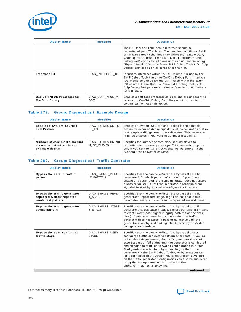
Display Name Identifier Description
Toolkit. Only one EMIF debug interface should beinstantiated per I/O column. You can chain additional EMIFor PHYLite cores to the first by enabling the "Enable Daisy-Chaining for Quartus Prime EMIF Debug Toolkit/On-ChipDebug Port" option for all cores in the chain, and selecting"Export" for the "Quartus Prime EMIF Debug Toolkit/On-ChipDebug Port" option on all cores after the first.
Interface ID DIAG_INTERFACE_ID Identifies interfaces within the I/O column, for use by theEMIF Debug Toolkit and the On-Chip Debug Port. InterfaceIDs should be unique among EMIF cores within the sameI/O column. If the Quartus Prime EMIF Debug Toolkit/On-Chip Debug Port parameter is set to Disabled, the interfaceID is unused.
Use Soft NIOS Processor forOn-Chip Debug
DIAG_SOFT_NIOS_MODE
Enables a soft Nios processor as a peripheral component toaccess the On-Chip Debug Port. Only one interface in acolumn can activate this option.
Table 279. Group: Diagnostics / Example Design
Display Name Identifier Description
Enable In-System-Sources-and-Probes
DIAG_EX_DESIGN_ISSP_EN
Enables In-System-Sources-and-Probes in the exampledesign for common debug signals, such as calibration statusor example traffic generator per-bit status. This parametermust be enabled if you want to do driver margining.
Number of core clocks sharingslaves to instantiate in theexample design
DIAG_EX_DESIGN_NUM_OF_SLAVES
Specifies the number of core clock sharing slaves toinstantiate in the example design. This parameter appliesonly if you set the "Core clocks sharing" parameter in the"General" tab to Master or Slave.
Table 280. Group: Diagnostics / Traffic Generator
Display Name Identifier Description
Bypass the default trafficpattern
DIAG_BYPASS_DEFAULT_PATTERN
Specifies that the controller/interface bypass the trafficgenerator 2.0 default pattern after reset. If you do notenable this parameter, the traffic generator does not asserta pass or fail status until the generator is configured andsignaled to start by its Avalon configuration interface.
Bypass the traffic generatorrepeated-writes/repeated-reads test pattern
DIAG_BYPASS_REPEAT_STAGE
Specifies that the controller/interface bypass the trafficgenerator's repeat test stage. If you do not enable thisparameter, every write and read is repeated several times.
Bypass the traffic generatorstress pattern
DIAG_BYPASS_STRESS_STAGE
Specifies that the controller/interface bypass the trafficgenerator's stress pattern stage. (Stress patterns are meantto create worst-case signal integrity patterns on the datapins.) If you do not enable this parameter, the trafficgenerator does not assert a pass or fail status until thegenerator is configured and signaled to start by its Avalonconfiguration interface.
Bypass the user-configuredtraffic stage
DIAG_BYPASS_USER_STAGE
Specifies that the controller/interface bypass the user-configured traffic generator's pattern after reset. If you donot enable this parameter, the traffic generator does notassert a pass or fail status until the generator is configuredand signaled to start by its Avalon configuration interface.Configuration can be done by connecting to the trafficgenerator via the EMIF Debug Toolkit, or by using customlogic connected to the Avalon-MM configuration slave porton the traffic generator. Configuration can also be simulatedusing the example testbench provided in thealtera_emif_avl_tg_2_tb.sv file.
continued...
7. Implementing and Parameterizing Memory IP
EMI_DG | 2017.05.08
External Memory Interface Handbook Volume 2: Design Guidelines Send Feedback
352
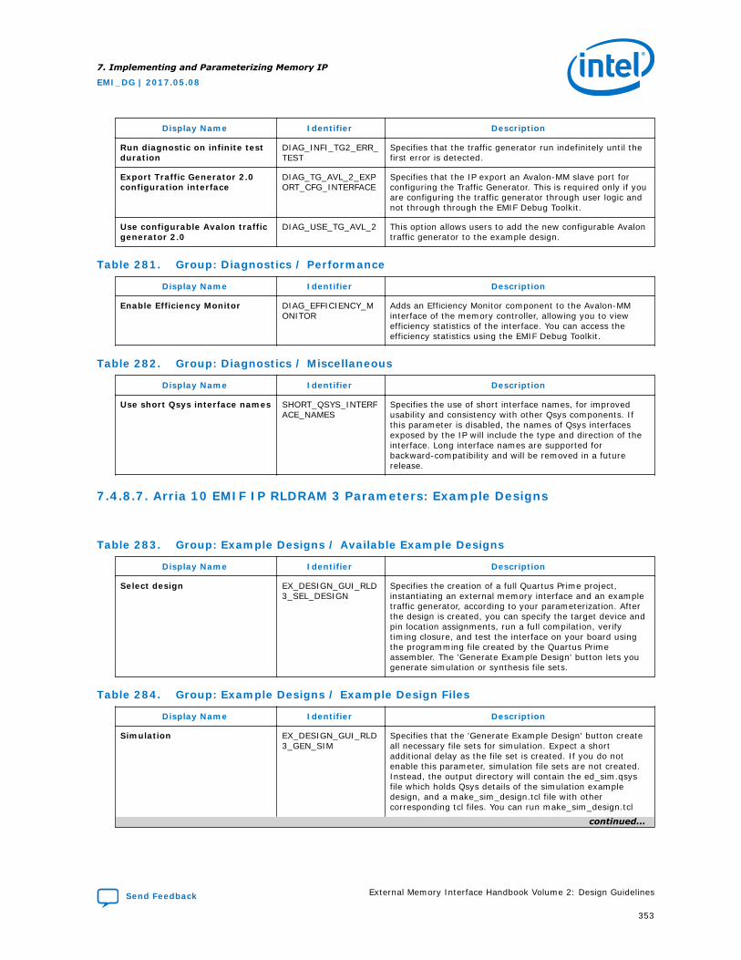
Display Name Identifier Description
Run diagnostic on infinite testduration
DIAG_INFI_TG2_ERR_TEST
Specifies that the traffic generator run indefinitely until thefirst error is detected.
Export Traffic Generator 2.0configuration interface
DIAG_TG_AVL_2_EXPORT_CFG_INTERFACE
Specifies that the IP export an Avalon-MM slave port forconfiguring the Traffic Generator. This is required only if youare configuring the traffic generator through user logic andnot through through the EMIF Debug Toolkit.
Use configurable Avalon trafficgenerator 2.0
DIAG_USE_TG_AVL_2 This option allows users to add the new configurable Avalontraffic generator to the example design.
Table 281. Group: Diagnostics / Performance
Display Name Identifier Description
Enable Efficiency Monitor DIAG_EFFICIENCY_MONITOR
Adds an Efficiency Monitor component to the Avalon-MMinterface of the memory controller, allowing you to viewefficiency statistics of the interface. You can access theefficiency statistics using the EMIF Debug Toolkit.
Table 282. Group: Diagnostics / Miscellaneous
Display Name Identifier Description
Use short Qsys interface names SHORT_QSYS_INTERFACE_NAMES
Specifies the use of short interface names, for improvedusability and consistency with other Qsys components. Ifthis parameter is disabled, the names of Qsys interfacesexposed by the IP will include the type and direction of theinterface. Long interface names are supported forbackward-compatibility and will be removed in a futurerelease.
7.4.8.7. Arria 10 EMIF IP RLDRAM 3 Parameters: Example Designs
Table 283. Group: Example Designs / Available Example Designs
Display Name Identifier Description
Select design EX_DESIGN_GUI_RLD3_SEL_DESIGN
Specifies the creation of a full Quartus Prime project,instantiating an external memory interface and an exampletraffic generator, according to your parameterization. Afterthe design is created, you can specify the target device andpin location assignments, run a full compilation, verifytiming closure, and test the interface on your board usingthe programming file created by the Quartus Primeassembler. The 'Generate Example Design' button lets yougenerate simulation or synthesis file sets.
Table 284. Group: Example Designs / Example Design Files
Display Name Identifier Description
Simulation EX_DESIGN_GUI_RLD3_GEN_SIM
Specifies that the 'Generate Example Design' button createall necessary file sets for simulation. Expect a shortadditional delay as the file set is created. If you do notenable this parameter, simulation file sets are not created.Instead, the output directory will contain the ed_sim.qsysfile which holds Qsys details of the simulation exampledesign, and a make_sim_design.tcl file with othercorresponding tcl files. You can run make_sim_design.tcl
continued...
7. Implementing and Parameterizing Memory IP
EMI_DG | 2017.05.08
Send Feedback External Memory Interface Handbook Volume 2: Design Guidelines
353

Display Name Identifier Description
from a command line to generate the simulation exampledesign. The generated example designs for varioussimulators are stored in the /sim sub-directory.
Synthesis EX_DESIGN_GUI_RLD3_GEN_SYNTH
Specifies that the 'Generate Example Design' button createall necessary file sets for synthesis. Expect a shortadditional delay as the file set is created. If you do notenable this parameter, synthesis file sets are not created.Instead, the output directory will contain the ed_synth.qsysfile which holds Qsys details of the synthesis exampledesign, and a make_qii_design.tcl script with othercorresponding tcl files. You can run make_qii_design.tclfrom a command line to generate the synthesis exampledesign. The generated example design is stored in the /qiisub-directory.
Table 285. Group: Example Designs / Generated HDL Format
Display Name Identifier Description
Simulation HDL format EX_DESIGN_GUI_RLD3_HDL_FORMAT
This option lets you choose the format of HDL in whichgenerated simulation files are created.
Table 286. Group: Example Designs / Target Development Kit
Display Name Identifier Description
Select board EX_DESIGN_GUI_RLD3_TARGET_DEV_KIT
Specifies that when you select a development kit with amemory module, the generated example design contains allsettings and fixed pin assignments to run on the selectedboard. You must select a development kit preset togenerate a working example design for the specifieddevelopment kit. Any IP settings not applied directly from adevelopment kit preset will not have guaranteed resultswhen testing the development kit. To exclude hardwaresupport of the example design, select 'none' from the'Select board' pull down menu. When you apply adevelopment kit preset, all IP parameters are automaticallyset appropriately to match the selected preset. If you wantto save your current settings, you should do so before youapply the preset. You can save your settings under adifferent name using File->Save as.
7.4.8.8. About Memory Presets
Presets help simplify the process of copying memory parameter values from memorydevice data sheets to the EMIF parameter editor.
For DDRx protocols, the memory presets are named using the following convention:
PROTOCOL-SPEEDBIN LATENCY FORMAT-AND-TOPOLOGY CAPACITY (INTERNAL-ORGANIZATION)
For example, the preset named DDR4-2666U CL18 Component 1CS 2Gb (512Mbx 4) refers to a DDR4 x4 component rated at the DDR4-2666U JEDEC speed bin, withnominal CAS latency of 18 cycles, one chip-select, and a total memory space of 2Gb.The JEDEC memory specification defines multiple speed bins for a given frequency(that is, DDR4-2666U and DDR4-2666V). You may be able to determine the exactspeed bin implemented by your memory device using its nominal latency. When indoubt, contact your memory vendor.
For RLDRAMx and QDRx protocols, the memory presets are named based on thevendor's device part number.
7. Implementing and Parameterizing Memory IP
EMI_DG | 2017.05.08
External Memory Interface Handbook Volume 2: Design Guidelines Send Feedback
354
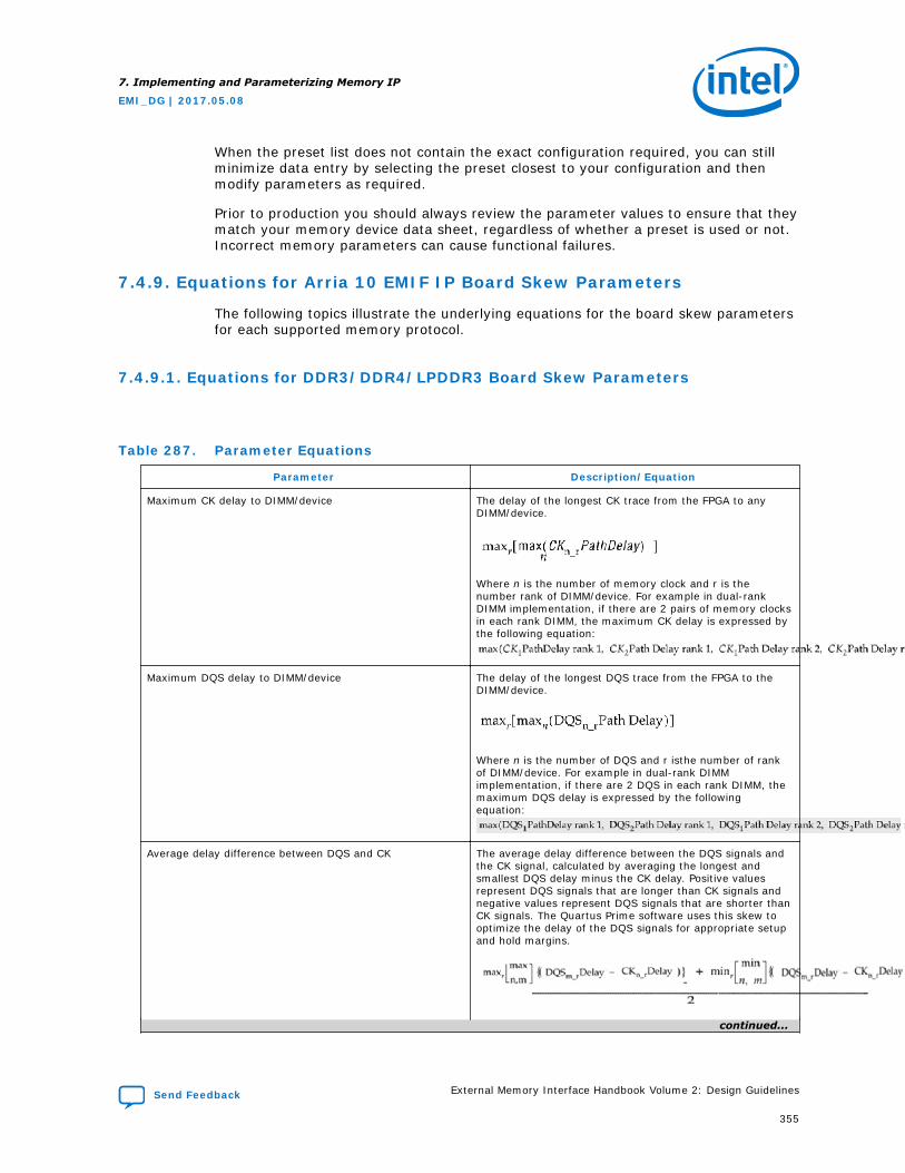
When the preset list does not contain the exact configuration required, you can stillminimize data entry by selecting the preset closest to your configuration and thenmodify parameters as required.
Prior to production you should always review the parameter values to ensure that theymatch your memory device data sheet, regardless of whether a preset is used or not.Incorrect memory parameters can cause functional failures.
7.4.9. Equations for Arria 10 EMIF IP Board Skew Parameters
The following topics illustrate the underlying equations for the board skew parametersfor each supported memory protocol.
7.4.9.1. Equations for DDR3/DDR4/LPDDR3 Board Skew Parameters
Table 287. Parameter Equations
Parameter Description/Equation
Maximum CK delay to DIMM/device The delay of the longest CK trace from the FPGA to anyDIMM/device.
Where n is the number of memory clock and r is thenumber rank of DIMM/device. For example in dual-rankDIMM implementation, if there are 2 pairs of memory clocksin each rank DIMM, the maximum CK delay is expressed bythe following equation:
Maximum DQS delay to DIMM/device The delay of the longest DQS trace from the FPGA to theDIMM/device.
Where n is the number of DQS and r isthe number of rankof DIMM/device. For example in dual-rank DIMMimplementation, if there are 2 DQS in each rank DIMM, themaximum DQS delay is expressed by the followingequation:
Average delay difference between DQS and CK The average delay difference between the DQS signals andthe CK signal, calculated by averaging the longest andsmallest DQS delay minus the CK delay. Positive valuesrepresent DQS signals that are longer than CK signals andnegative values represent DQS signals that are shorter thanCK signals. The Quartus Prime software uses this skew tooptimize the delay of the DQS signals for appropriate setupand hold margins.
continued...
7. Implementing and Parameterizing Memory IP
EMI_DG | 2017.05.08
Send Feedback External Memory Interface Handbook Volume 2: Design Guidelines
355
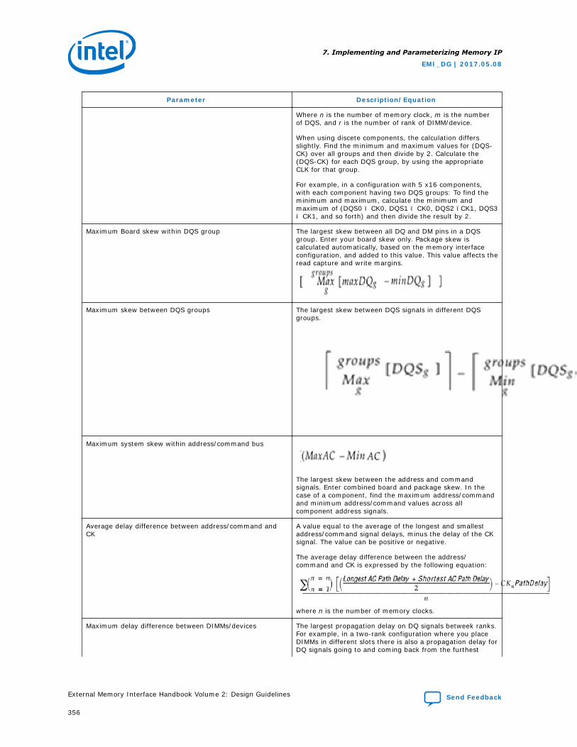
Parameter Description/Equation
Where n is the number of memory clock, m is the numberof DQS, and r is the number of rank of DIMM/device.
When using discete components, the calculation differsslightly. Find the minimum and maximum values for (DQS-CK) over all groups and then divide by 2. Calculate the(DQS-CK) for each DQS group, by using the appropriateCLK for that group.
For example, in a configuration with 5 x16 components,with each component having two DQS groups: To find theminimum and maximum, calculate the minimum andmaximum of (DQS0 – CK0, DQS1 – CK0, DQS2 –CK1, DQS3– CK1, and so forth) and then divide the result by 2.
Maximum Board skew within DQS group The largest skew between all DQ and DM pins in a DQSgroup. Enter your board skew only. Package skew iscalculated automatically, based on the memory interfaceconfiguration, and added to this value. This value affects theread capture and write margins.
Maximum skew between DQS groups The largest skew between DQS signals in different DQSgroups.
Maximum system skew within address/command bus
The largest skew between the address and commandsignals. Enter combined board and package skew. In thecase of a component, find the maximum address/commandand minimum address/command values across allcomponent address signals.
Average delay difference between address/command andCK
A value equal to the average of the longest and smallestaddress/command signal delays, minus the delay of the CKsignal. The value can be positive or negative.
The average delay difference between the address/command and CK is expressed by the following equation:
where n is the number of memory clocks.
Maximum delay difference between DIMMs/devices The largest propagation delay on DQ signals betweek ranks.For example, in a two-rank configuration where you placeDIMMs in different slots there is also a propagation delay forDQ signals going to and coming back from the furthest
7. Implementing and Parameterizing Memory IP
EMI_DG | 2017.05.08
External Memory Interface Handbook Volume 2: Design Guidelines Send Feedback
356
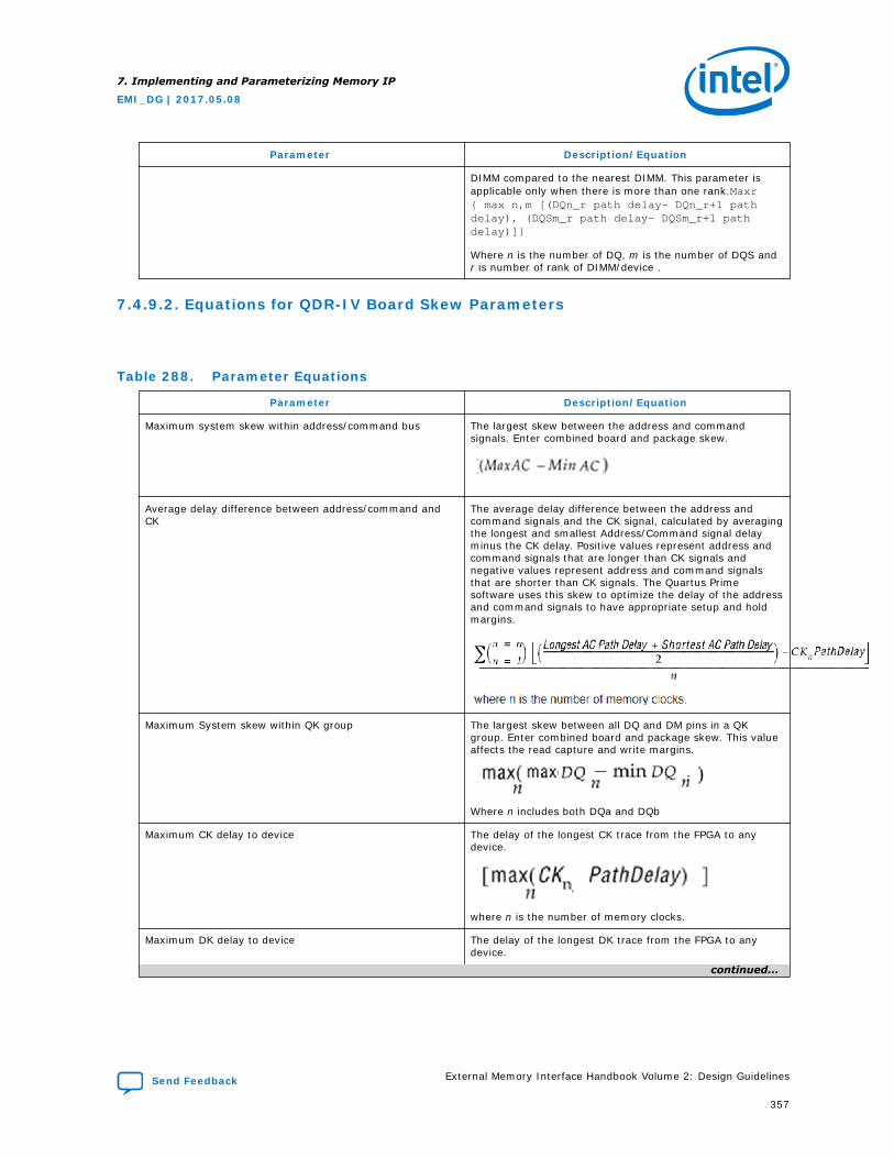
Parameter Description/Equation
DIMM compared to the nearest DIMM. This parameter isapplicable only when there is more than one rank.Maxr max n,m [(DQn_r path delay– DQn_r+1 pathdelay), (DQSm_r path delay– DQSm_r+1 pathdelay)]
Where n is the number of DQ, m is the number of DQS andr is number of rank of DIMM/device .
7.4.9.2. Equations for QDR-IV Board Skew Parameters
Table 288. Parameter Equations
Parameter Description/Equation
Maximum system skew within address/command bus The largest skew between the address and commandsignals. Enter combined board and package skew.
Average delay difference between address/command andCK
The average delay difference between the address andcommand signals and the CK signal, calculated by averagingthe longest and smallest Address/Command signal delayminus the CK delay. Positive values represent address andcommand signals that are longer than CK signals andnegative values represent address and command signalsthat are shorter than CK signals. The Quartus Primesoftware uses this skew to optimize the delay of the addressand command signals to have appropriate setup and holdmargins.
Maximum System skew within QK group The largest skew between all DQ and DM pins in a QKgroup. Enter combined board and package skew. This valueaffects the read capture and write margins.
Where n includes both DQa and DQb
Maximum CK delay to device The delay of the longest CK trace from the FPGA to anydevice.
where n is the number of memory clocks.
Maximum DK delay to device The delay of the longest DK trace from the FPGA to anydevice.
continued...
7. Implementing and Parameterizing Memory IP
EMI_DG | 2017.05.08
Send Feedback External Memory Interface Handbook Volume 2: Design Guidelines
357
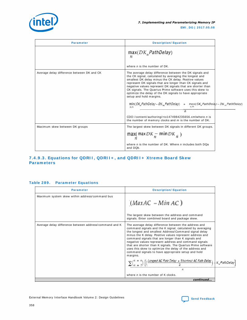
Parameter Description/Equation
where n is the number of DK.
Average delay difference between DK and CK The average delay difference between the DK signals andthe CK signal, calculated by averaging the longest andsmallest DK delay minus the CK delay. Positive valuesrepresent DK signals that are longer than CK signals andnegative values represent DK signals that are shorter thanCK signals. The Quartus Prime software uses this skew tooptimize the delay of the DK signals to have appropriatesetup and hold margins.
CDO:/content/authoring/rto1474984235656.xmlwhere n isthe number of memory clocks and m is the number of DK.
Maximum skew between DK groups The largest skew between DK signals in different DK groups.
where n is the number of DK. Where n includes both DQaand DQb.
7.4.9.3. Equations for QDRII, QDRII+, and QDRII+ Xtreme Board SkewParameters
Table 289. Parameter Equations
Parameter Description/Equation
Maximum system skew within address/command bus
The largest skew between the address and commandsignals. Enter combined board and package skew.
Average delay difference between address/command and K The average delay difference between the address andcommand signals and the K signal, calculated by averagingthe longest and smallest Address/Command signal delayminus the K delay. Positive values represent address andcommand signals that are longer than K signals andnegative values represent address and command signalsthat are shorter than K signals. The Quartus Prime softwareuses this skew to optimize the delay of the address andcommand signals to have appropriate setup and holdmargins.
where n is the number of K clocks.
continued...
7. Implementing and Parameterizing Memory IP
EMI_DG | 2017.05.08
External Memory Interface Handbook Volume 2: Design Guidelines Send Feedback
358
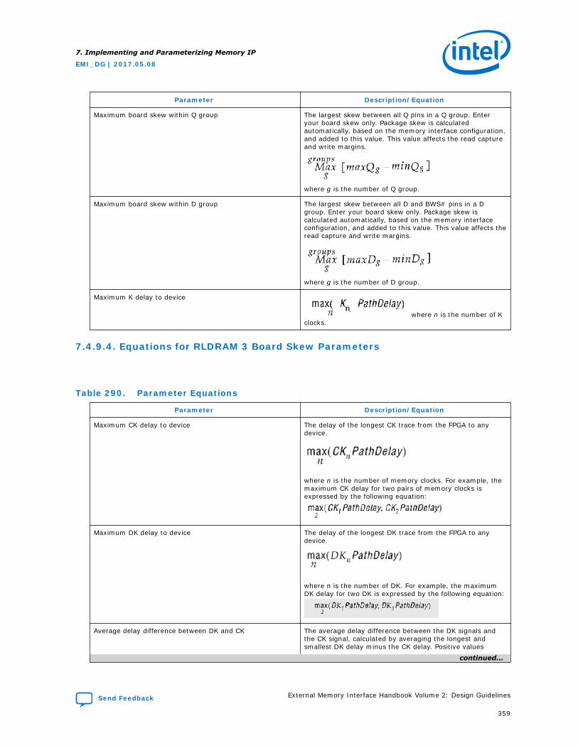
Parameter Description/Equation
Maximum board skew within Q group The largest skew between all Q pins in a Q group. Enteryour board skew only. Package skew is calculatedautomatically, based on the memory interface configuration,and added to this value. This value affects the read captureand write margins.
where g is the number of Q group.
Maximum board skew within D group The largest skew between all D and BWS# pins in a Dgroup. Enter your board skew only. Package skew iscalculated automatically, based on the memory interfaceconfiguration, and added to this value. This value affects theread capture and write margins.
where g is the number of D group.
Maximum K delay to device
where n is the number of Kclocks.
7.4.9.4. Equations for RLDRAM 3 Board Skew Parameters
Table 290. Parameter Equations
Parameter Description/Equation
Maximum CK delay to device The delay of the longest CK trace from the FPGA to anydevice.
where n is the number of memory clocks. For example, themaximum CK delay for two pairs of memory clocks isexpressed by the following equation:
Maximum DK delay to device The delay of the longest DK trace from the FPGA to anydevice.
where n is the number of DK. For example, the maximumDK delay for two DK is expressed by the following equation:
Average delay difference between DK and CK The average delay difference between the DK signals andthe CK signal, calculated by averaging the longest andsmallest DK delay minus the CK delay. Positive values
continued...
7. Implementing and Parameterizing Memory IP
EMI_DG | 2017.05.08
Send Feedback External Memory Interface Handbook Volume 2: Design Guidelines
359
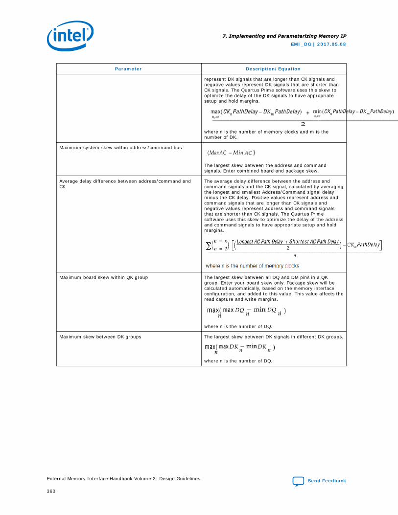
Parameter Description/Equation
represent DK signals that are longer than CK signals andnegative values represent DK signals that are shorter thanCK signals. The Quartus Prime software uses this skew tooptimize the delay of the DK signals to have appropriatesetup and hold margins.
where n is the number of memory clocks and m is thenumber of DK.
Maximum system skew within address/command bus
The largest skew between the address and commandsignals. Enter combined board and package skew.
Average delay difference between address/command andCK
The average delay difference between the address andcommand signals and the CK signal, calculated by averagingthe longest and smallest Address/Command signal delayminus the CK delay. Positive values represent address andcommand signals that are longer than CK signals andnegative values represent address and command signalsthat are shorter than CK signals. The Quartus Primesoftware uses this skew to optimize the delay of the addressand command signals to have appropriate setup and holdmargins.
Maximum board skew within QK group The largest skew between all DQ and DM pins in a QKgroup. Enter your board skew only. Package skew will becalculated automatically, based on the memory interfaceconfiguration, and added to this value. This value affects theread capture and write margins.
where n is the number of DQ.
Maximum skew between DK groups The largest skew between DK signals in different DK groups.
where n is the number of DQ.
7. Implementing and Parameterizing Memory IP
EMI_DG | 2017.05.08
External Memory Interface Handbook Volume 2: Design Guidelines Send Feedback
360
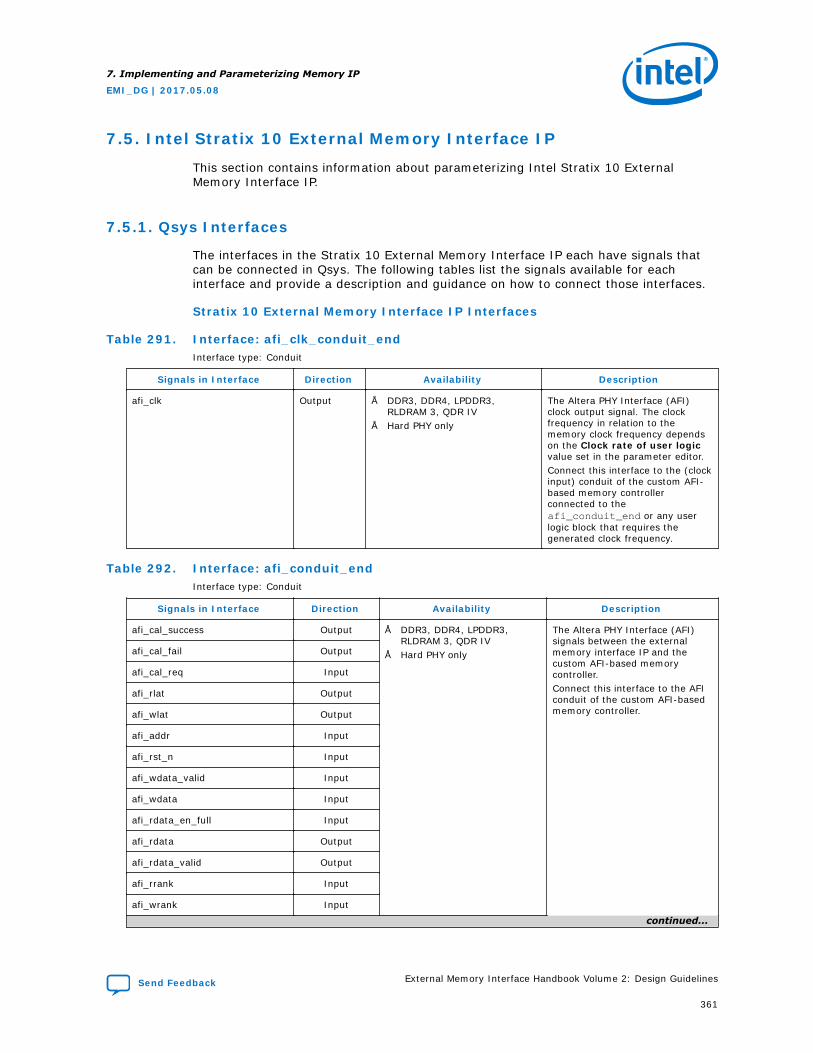
7.5. Intel Stratix 10 External Memory Interface IP
This section contains information about parameterizing Intel Stratix 10 ExternalMemory Interface IP.
7.5.1. Qsys Interfaces
The interfaces in the Stratix 10 External Memory Interface IP each have signals thatcan be connected in Qsys. The following tables list the signals available for eachinterface and provide a description and guidance on how to connect those interfaces.
Stratix 10 External Memory Interface IP Interfaces
Table 291. Interface: afi_clk_conduit_endInterface type: Conduit
Signals in Interface Direction Availability Description
afi_clk Output • DDR3, DDR4, LPDDR3,RLDRAM 3, QDR IV
• Hard PHY only
The Altera PHY Interface (AFI)clock output signal. The clockfrequency in relation to thememory clock frequency dependson the Clock rate of user logicvalue set in the parameter editor.Connect this interface to the (clockinput) conduit of the custom AFI-based memory controllerconnected to theafi_conduit_end or any userlogic block that requires thegenerated clock frequency.
Table 292. Interface: afi_conduit_endInterface type: Conduit
Signals in Interface Direction Availability Description
afi_cal_success Output • DDR3, DDR4, LPDDR3,RLDRAM 3, QDR IV
• Hard PHY only
The Altera PHY Interface (AFI)signals between the externalmemory interface IP and thecustom AFI-based memorycontroller.Connect this interface to the AFIconduit of the custom AFI-basedmemory controller.
afi_cal_fail Output
afi_cal_req Input
afi_rlat Output
afi_wlat Output
afi_addr Input
afi_rst_n Input
afi_wdata_valid Input
afi_wdata Input
afi_rdata_en_full Input
afi_rdata Output
afi_rdata_valid Output
afi_rrank Input
afi_wrank Input
continued...
7. Implementing and Parameterizing Memory IP
EMI_DG | 2017.05.08
Send Feedback External Memory Interface Handbook Volume 2: Design Guidelines
361
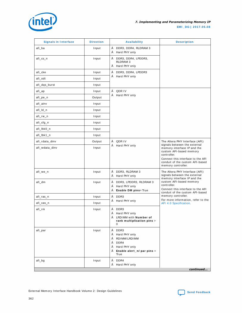
Signals in Interface Direction Availability Description
afi_ba Input • DDR3, DDR4, RLDRAM 3• Hard PHY only
afi_cs_n Input • DDR3, DDR4, LPDDR3,RLDRAM 3
• Hard PHY only
afi_cke Input • DDR3, DDR4, LPDDR3• Hard PHY only
afi_odt Input
afi_dqs_burst Input
afi_ap Input • QDR IV• Hard PHY only
afi_pe_n Output
afi_ainv Input
afi_ld_n Input
afi_rw_n Input
afi_cfg_n Input
afi_lbk0_n Input
afi_lbk1_n Input
afi_rdata_dinv Output • QDR IV• Hard PHY only
The Altera PHY Interface (AFI)signals between the externalmemory interface IP and thecustom AFI-based memorycontroller.Connect this interface to the AFIconduit of the custom AFI-basedmemory controller.
afi_wdata_dinv Input
afi_we_n Input • DDR3, RLDRAM 3• Hard PHY only
The Altera PHY Interface (AFI)signals between the externalmemory interface IP and thecustom AFI-based memorycontroller.Connect this interface to the AFIconduit of the custom AFI-basedmemory controller.For more information, refer to the AFI 4.0 Specification.
afi_dm Input • DDR3, LPDDR3, RLDRAM 3• Hard PHY only• Enable DM pins=True
afi_ras_n Input • DDR3• Hard PHY only
afi_cas_n Input
afi_rm Input • DDR3• Hard PHY only• LRDIMM with Number of
rank multiplication pins >0
afi_par Input • DDR3• Hard PHY only• RDIMM/LRDIMM• DDR4• Hard PHY only• Enable alert_n/par pins =
True
afi_bg Input • DDR4• Hard PHY only
continued...
7. Implementing and Parameterizing Memory IP
EMI_DG | 2017.05.08
External Memory Interface Handbook Volume 2: Design Guidelines Send Feedback
362
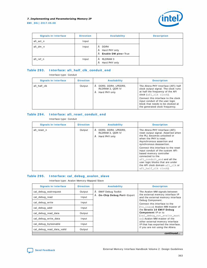
Signals in Interface Direction Availability Description
afi_act_n Input
afi_dm_n Input • DDR4• Hard PHY only• Enable DM pins=True
afi_ref_n Input • RLDRAM 3• Hard PHY only
Table 293. Interface: afi_half_clk_conduit_endInterface type: Conduit
Signals in Interface Direction Availability Description
afi_half_clk Output • DDR3, DDR4, LPDDR3,RLDRAM 3, QDR IV
• Hard PHY only
The Altera PHY Interface (AFI) halfclock output signal. The clock runsat half the frequency of the AFIclock (afi_clk clock).Connect this interface to the clockinput conduit of the user logicblock that needs to be clocked atthe generated clock frequency.
Table 294. Interface: afi_reset_conduit_endInterface type: Conduit
Signals in Interface Direction Availability Description
afi_reset_n Output • DDR3, DDR4, LPDDR3,RLDRAM 3, QDR IV
• Hard PHY only
The Altera PHY Interface (AFI)reset output signal. Asserted whenthe PLL becomes unlocked orwhen the PHY is reset.Asynchronous assertion andsynchronous deassertion.Connect this interface to the resetinput conduit of the custom AFI-based memory controllerconnected to theafi_conduit_end and all theuser logic blocks that are underthe AFI clock domain afi_clk orafi_half_clk clock).
Table 295. Interface: cal_debug_avalon_slaveInterface type: Avalon Memory-Mapped Slave
Signals in Interface Direction Availability Description
cal_debug_waitrequest Output • EMIF Debug Toolkit• On-Chip Debug Port=Export
The Avalon-MM signals betweenthe external memory interface IPand the external memory interfaceDebug Component.Connect this interface to the(to_ioaux) Avalon-MM master ofthe Stratix 10 EMIF DebugComponent IP or to(cal_debug_out_avalon_master) Avalon-MM master of theother external memory interfaceIP that has exported the interface.If you are not using the Altera
cal_debug_read Input
cal_debug_write Input
cal_debug_addr Input
cal_debug_read_data Output
cal_debug_write_data Input
cal_debug_byteenable Input
cal_debug_read_data_valid Outputcontinued...
7. Implementing and Parameterizing Memory IP
EMI_DG | 2017.05.08
Send Feedback External Memory Interface Handbook Volume 2: Design Guidelines
363
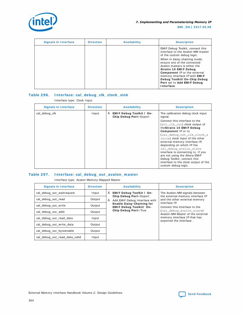
Signals in Interface Direction Availability Description
EMIF Debug Toolkit, connect thisinterface to the Avalon-MM masterof the custom debug logic.When in daisy-chaining mode,ensure one of the connectedAvalon masters is either theStratix 10 EMIF DebugComponent IP or the externalmemory interface IP with EMIFDebug Toolkit/On-Chip DebugPort set to Add EMIF DebugInterface.
Table 296. Interface: cal_debug_clk_clock_sinkInterface type: Clock Input
Signals in Interface Direction Availability Description
cal_debug_clk Input • EMIF Debug Toolkit / On-Chip Debug Port=Export
The calibration debug clock inputsignal.Connect this interface to the(avl_clk_out) clock output oftheStratix 10 EMIF DebugComponent IP or to(cal_debug_out_clk_clock_source) clock input of the otherexternal memory interface IP,depending on which IP thecal_debug_avalon_slaveinterface is connecting to. If youare not using the Altera EMIFDebug Toolkit, connect thisinterface to the clock output of thecustom debug logic.
Table 297. Interface: cal_debug_out_avalon_masterInterface type: Avalon Memory-Mapped Master
Signals in Interface Direction Availability Description
cal_debug_out_waitrequest Input • EMIF Debug Toolkit / On-Chip Debug Port=Export
• Add EMIF Debug Interface withEnable Daisy-Chaining forEMIF Debug Toolkit/ On-Chip Debug Port=True
The Avalon-MM signals betweenthe external memory interface IPand the other external memoryinterface IP.Connect this interface to the(cal_debug_avalon_slave)Avalon-MM Master of the externalmemory interface IP that hasexported the interface .
cal_debug_out_read Output
cal_debug_out_write Output
cal_debug_out_addr Output
cal_debug_out_read_data Input
cal_debug_out_write_data Output
cal_debug_out_byteenable Output
cal_debug_out_read_data_valid Input
7. Implementing and Parameterizing Memory IP
EMI_DG | 2017.05.08
External Memory Interface Handbook Volume 2: Design Guidelines Send Feedback
364
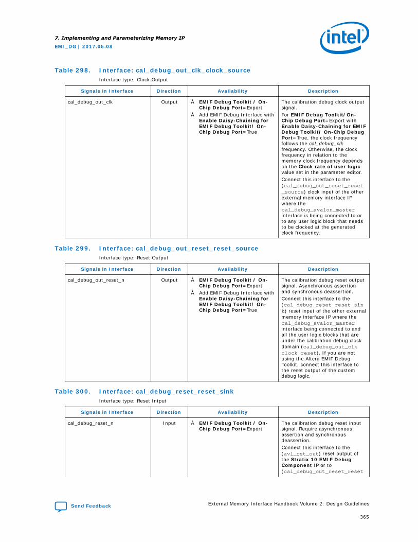
Table 298. Interface: cal_debug_out_clk_clock_sourceInterface type: Clock Output
Signals in Interface Direction Availability Description
cal_debug_out_clk Output • EMIF Debug Toolkit / On-Chip Debug Port=Export
• Add EMIF Debug Interface withEnable Daisy-Chaining forEMIF Debug Toolkit/ On-Chip Debug Port=True
The calibration debug clock outputsignal.For EMIF Debug Toolkit/On-Chip Debug Port=Export withEnable Daisy-Chaining for EMIFDebug Toolkit/ On-Chip DebugPort=True, the clock frequencyfollows the cal_debug_clkfrequency. Otherwise, the clockfrequency in relation to thememory clock frequency dependson the Clock rate of user logicvalue set in the parameter editor.Connect this interface to the(cal_debug_out_reset_reset_source) clock input of the otherexternal memory interface IPwhere thecal_debug_avalon_masterinterface is being connected to orto any user logic block that needsto be clocked at the generatedclock frequency.
Table 299. Interface: cal_debug_out_reset_reset_sourceInterface type: Reset Output
Signals in Interface Direction Availability Description
cal_debug_out_reset_n Output • EMIF Debug Toolkit / On-Chip Debug Port=Export
• Add EMIF Debug Interface withEnable Daisy-Chaining forEMIF Debug Toolkit/ On-Chip Debug Port=True
The calibration debug reset outputsignal. Asynchronous assertionand synchronous deassertion.Connect this interface to the(cal_debug_reset_reset_sink) reset input of the other externalmemory interface IP where thecal_debug_avalon_masterinterface being connected to andall the user logic blocks that areunder the calibration debug clockdomain (cal_debug_out_clkclock reset). If you are notusing the Altera EMIF DebugToolkit, connect this interface tothe reset output of the customdebug logic.
Table 300. Interface: cal_debug_reset_reset_sinkInterface type: Reset Intput
Signals in Interface Direction Availability Description
cal_debug_reset_n Input • EMIF Debug Toolkit / On-Chip Debug Port=Export
The calibration debug reset inputsignal. Require asynchronousassertion and synchronousdeassertion.Connect this interface to the(avl_rst_out) reset output ofthe Stratix 10 EMIF DebugComponent IP or to(cal_debug_out_reset_reset
7. Implementing and Parameterizing Memory IP
EMI_DG | 2017.05.08
Send Feedback External Memory Interface Handbook Volume 2: Design Guidelines
365
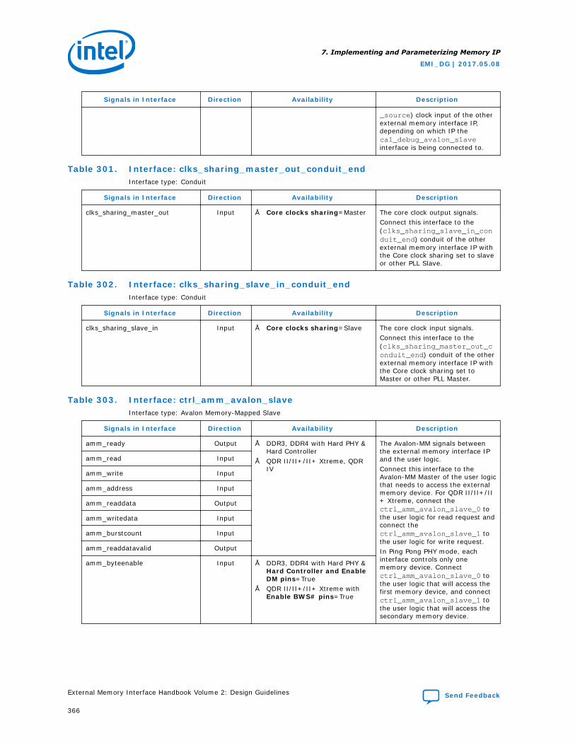
Signals in Interface Direction Availability Description
_source) clock input of the otherexternal memory interface IP,depending on which IP thecal_debug_avalon_slaveinterface is being connected to.
Table 301. Interface: clks_sharing_master_out_conduit_endInterface type: Conduit
Signals in Interface Direction Availability Description
clks_sharing_master_out Input • Core clocks sharing=Master The core clock output signals.Connect this interface to the(clks_sharing_slave_in_conduit_end) conduit of the otherexternal memory interface IP withthe Core clock sharing set to slaveor other PLL Slave.
Table 302. Interface: clks_sharing_slave_in_conduit_endInterface type: Conduit
Signals in Interface Direction Availability Description
clks_sharing_slave_in Input • Core clocks sharing=Slave The core clock input signals.Connect this interface to the(clks_sharing_master_out_conduit_end) conduit of the otherexternal memory interface IP withthe Core clock sharing set toMaster or other PLL Master.
Table 303. Interface: ctrl_amm_avalon_slaveInterface type: Avalon Memory-Mapped Slave
Signals in Interface Direction Availability Description
amm_ready Output • DDR3, DDR4 with Hard PHY &Hard Controller
• QDR II/II+/II+ Xtreme, QDRIV
The Avalon-MM signals betweenthe external memory interface IPand the user logic.Connect this interface to theAvalon-MM Master of the user logicthat needs to access the externalmemory device. For QDR II/II+/II+ Xtreme, connect thectrl_amm_avalon_slave_0 tothe user logic for read request andconnect thectrl_amm_avalon_slave_1 tothe user logic for write request.In Ping Pong PHY mode, eachinterface controls only onememory device. Connectctrl_amm_avalon_slave_0 tothe user logic that will access thefirst memory device, and connectctrl_amm_avalon_slave_1 tothe user logic that will access thesecondary memory device.
amm_read Input
amm_write Input
amm_address Input
amm_readdata Output
amm_writedata Input
amm_burstcount Input
amm_readdatavalid Output
amm_byteenable Input • DDR3, DDR4 with Hard PHY &Hard Controller and EnableDM pins=True
• QDR II/II+/II+ Xtreme withEnable BWS# pins=True
7. Implementing and Parameterizing Memory IP
EMI_DG | 2017.05.08
External Memory Interface Handbook Volume 2: Design Guidelines Send Feedback
366
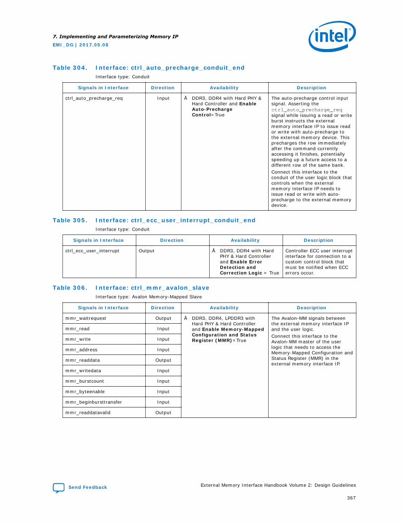
Table 304. Interface: ctrl_auto_precharge_conduit_endInterface type: Conduit
Signals in Interface Direction Availability Description
ctrl_auto_precharge_req Input • DDR3, DDR4 with Hard PHY &Hard Controller and EnableAuto-PrechargeControl=True
The auto-precharge control inputsignal. Asserting thectrl_auto_precharge_reqsignal while issuing a read or writeburst instructs the externalmemory interface IP to issue reador write with auto-precharge tothe external memory device. Thisprecharges the row immediatelyafter the command currentlyaccessing it finishes, potentiallyspeeding up a future access to adifferent row of the same bank.Connect this interface to theconduit of the user logic block thatcontrols when the externalmemory interface IP needs toissue read or write with auto-precharge to the external memorydevice.
Table 305. Interface: ctrl_ecc_user_interrupt_conduit_endInterface type: Conduit
Signals in Interface Direction Availability Description
ctrl_ecc_user_interrupt Output • DDR3, DDR4 with HardPHY & Hard Controllerand Enable ErrorDetection andCorrection Logic = True
Controller ECC user interruptinterface for connection to acustom control block thatmust be notified when ECCerrors occur.
Table 306. Interface: ctrl_mmr_avalon_slaveInterface type: Avalon Memory-Mapped Slave
Signals in Interface Direction Availability Description
mmr_waitrequest Output • DDR3, DDR4, LPDDR3 withHard PHY & Hard Controllerand Enable Memory-MappedConfiguration and StatusRegister (MMR)=True
The Avalon-MM signals betweenthe external memory interface IPand the user logic.Connect this interface to theAvalon-MM master of the userlogic that needs to access theMemory-Mapped Configuration andStatus Register (MMR) in theexternal memory interface IP.
mmr_read Input
mmr_write Input
mmr_address Input
mmr_readdata Output
mmr_writedata Input
mmr_burstcount Input
mmr_byteenable Input
mmr_beginbursttransfer Input
mmr_readdatavalid Output
7. Implementing and Parameterizing Memory IP
EMI_DG | 2017.05.08
Send Feedback External Memory Interface Handbook Volume 2: Design Guidelines
367
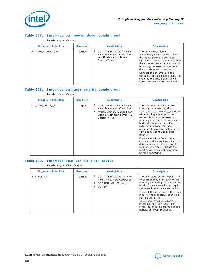
Table 307. Interface: ctrl_power_down_conduit_endInterface type: Conduit
Signals in Interface Direction Availability Description
ctrl_power_down_ack Output • DDR3, DDR4, LPDDR3 withHard PHY & Hard Controllerand Enable Auto PowerDown=True
The auto power-downacknowledgment signals. Whenthe ctrl_power_down_acksignal is asserted, it indicates thatthe external memory interface IPis placing the external memorydevice into power-down mode.Connect this interface to theconduit of the user logic block thatrequires the auto power-downstatus, or leave it unconnected.
Table 308. Interface: ctrl_user_priority_conduit_endInterface type: Conduit
Signals in Interface Direction Availability Description
ctrl_user_priority_hi Input • DDR3, DDR4, LPDDR3 withHard PHY & Hard Controller
• Avalon Memory-Mapped andEnable Command PriorityControl=true
The command priority controlinput signal. Asserting thectrl_user_priority_hi signalwhile issuing a read or writerequest instructs the externalmemory interface to treat it as ahigh-priority command. Theexternal memory interfaceattempts to execute high-prioritycommands sooner, to reducelatency.Connect this interface to theconduit of the user logic block thatdetermines when the externalmemory interface IP treats theread or write request as a high-priority command.
Table 309. Interface: emif_usr_clk_clock_sourceInterface type: Clock Output
Signals in Interface Direction Availability Description
emif_usr_clk Output • DDR3, DDR4, LPDDR3, withHard PHY & Hard Controller
• QDR II/II+/II+ Xtreme• QDR IV
The user clock output signal. Theclock frequency in relation to thememory clock frequency dependson the Clock rate of user logicvalue set in the parameter editor.Connect this interface to the clockinput of the respective user logicconnected to thectrl_amm_avalon_slave_0interface, or to any user logicblock that must be clocked at thegenerated clock frequency.
7. Implementing and Parameterizing Memory IP
EMI_DG | 2017.05.08
External Memory Interface Handbook Volume 2: Design Guidelines Send Feedback
368
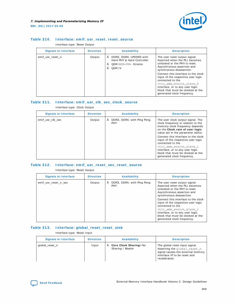
Table 310. Interface: emif_usr_reset_reset_sourceInterface type: Reset Output
Signals in Interface Direction Availability Description
emif_usr_reset_n Output • DDR3, DDR4, LPDDR3 withHard PHY & Hard Controller
• QDR II/II+/II+ Xtreme• QDR IV
The user reset output signal.Asserted when the PLL becomesunlocked or the PHY is reset.Asynchronous assertion andsynchronous deassertion.Connect this interface to the clockinput of the respective user logicconnected to thectrl_amm_avalon_slave_0interface, or to any user logicblock that must be clocked at thegenerated clock frequency.
Table 311. Interface: emif_usr_clk_sec_clock_sourceInterface type: Clock Output
Signals in Interface Direction Availability Description
emif_usr_clk_sec Output • DDR3, DDR4, with Ping PongPHY
The user clock output signal. Theclock frequency in relation to thememory clock frequency dependson the Clock rate of user logicvalue set in the parameter editor.Connect this interface to the clockinput of the respective user logicconnected to thectrl_amm_avalon_slave_1interface, or to any user logicblock that must be clocked at thegenerated clock frequency.
Table 312. Interface: emif_usr_reset_sec_reset_sourceInterface type: Reset Output
Signals in Interface Direction Availability Description
emif_usr_reset_n_sec Output • DDR3, DDR4, with Ping PongPHY
The user reset output signal.Asserted when the PLL becomesunlocked or the PHY is reset.Asynchronous assertion andsynchronous deassertion.Connect this interface to the clockinput of the respective user logicconnected to thectrl_amm_avalon_slave_1interface, or to any user logicblock that must be clocked at thegenerated clock frequency.
Table 313. Interface: global_reset_reset_sinkInterface type: Reset Input
Signals in Interface Direction Availability Description
global_reset_n Input • Core Clock Sharing=NoSharing / Master
The global reset input signal.Asserting the global_reset_nsignal causes the external memoryinterface IP to be reset andrecalibrated.
7. Implementing and Parameterizing Memory IP
EMI_DG | 2017.05.08
Send Feedback External Memory Interface Handbook Volume 2: Design Guidelines
369
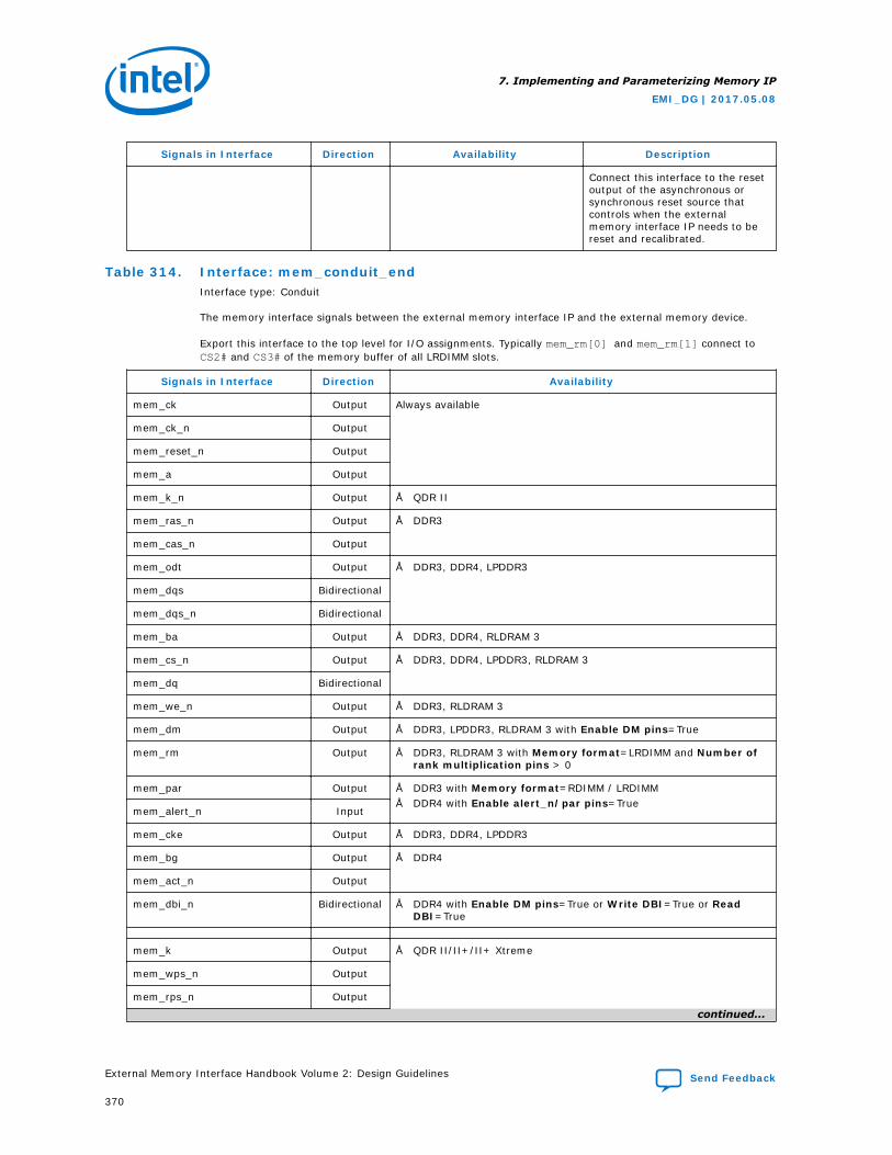
Signals in Interface Direction Availability Description
Connect this interface to the resetoutput of the asynchronous orsynchronous reset source thatcontrols when the externalmemory interface IP needs to bereset and recalibrated.
Table 314. Interface: mem_conduit_endInterface type: Conduit
The memory interface signals between the external memory interface IP and the external memory device.
Export this interface to the top level for I/O assignments. Typically mem_rm[0] and mem_rm[1] connect toCS2# and CS3# of the memory buffer of all LRDIMM slots.
Signals in Interface Direction Availability
mem_ck Output Always available
mem_ck_n Output
mem_reset_n Output
mem_a Output
mem_k_n Output • QDR II
mem_ras_n Output • DDR3
mem_cas_n Output
mem_odt Output • DDR3, DDR4, LPDDR3
mem_dqs Bidirectional
mem_dqs_n Bidirectional
mem_ba Output • DDR3, DDR4, RLDRAM 3
mem_cs_n Output • DDR3, DDR4, LPDDR3, RLDRAM 3
mem_dq Bidirectional
mem_we_n Output • DDR3, RLDRAM 3
mem_dm Output • DDR3, LPDDR3, RLDRAM 3 with Enable DM pins=True
mem_rm Output • DDR3, RLDRAM 3 with Memory format=LRDIMM and Number ofrank multiplication pins > 0
mem_par Output • DDR3 with Memory format=RDIMM / LRDIMM• DDR4 with Enable alert_n/par pins=True
mem_alert_n Input
mem_cke Output • DDR3, DDR4, LPDDR3
mem_bg Output • DDR4
mem_act_n Output
mem_dbi_n Bidirectional • DDR4 with Enable DM pins=True or Write DBI=True or ReadDBI=True
mem_k Output • QDR II/II+/II+ Xtreme
mem_wps_n Output
mem_rps_n Output
continued...
7. Implementing and Parameterizing Memory IP
EMI_DG | 2017.05.08
External Memory Interface Handbook Volume 2: Design Guidelines Send Feedback
370
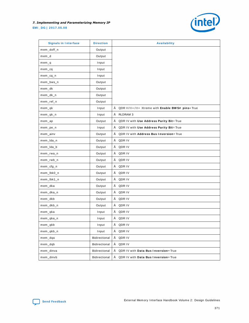
Signals in Interface Direction Availability
mem_doff_n Output
mem_d Output
mem_q Input
mem_cq Input
mem_cq_n Input
mem_bws_n Output
mem_dk Output
mem_dk_n Output
mem_ref_n Output
mem_qk Input • QDR II/II+/II+ Xtreme with Enable BWS# pins=True
mem_qk_n Input • RLDRAM 3
mem_ap Output • QDR IV with Use Address Parity Bit=True
mem_pe_n Input • QDR IV with Use Address Parity Bit=True
mem_ainv Output • QDR IV with Address Bus Inversion=True
mem_lda_n Output • QDR IV
mem_lda_b Output • QDR IV
mem_rwa_n Output • QDR IV
mem_rwb_n Output • QDR IV
mem_cfg_n Output • QDR IV
mem_lbk0_n Output • QDR IV
mem_lbk1_n Output • QDR IV
mem_dka Output • QDR IV
mem_dka_n Output • QDR IV
mem_dkb Output • QDR IV
mem_dkb_n Output • QDR IV
mem_qka Input • QDR IV
mem_qka_n Input • QDR IV
mem_qkb Input • QDR IV
mem_qkb_n Input • QDR IV
mem_dqa Bidirectional • QDR IV
mem_dqb Bidirectional • QDR IV
mem_dinva Bidirectional • QDR IV with Data Bus Inversion=True
mem_dinvb Bidirectional • QDR IV with Data Bus Inversion=True
7. Implementing and Parameterizing Memory IP
EMI_DG | 2017.05.08
Send Feedback External Memory Interface Handbook Volume 2: Design Guidelines
371
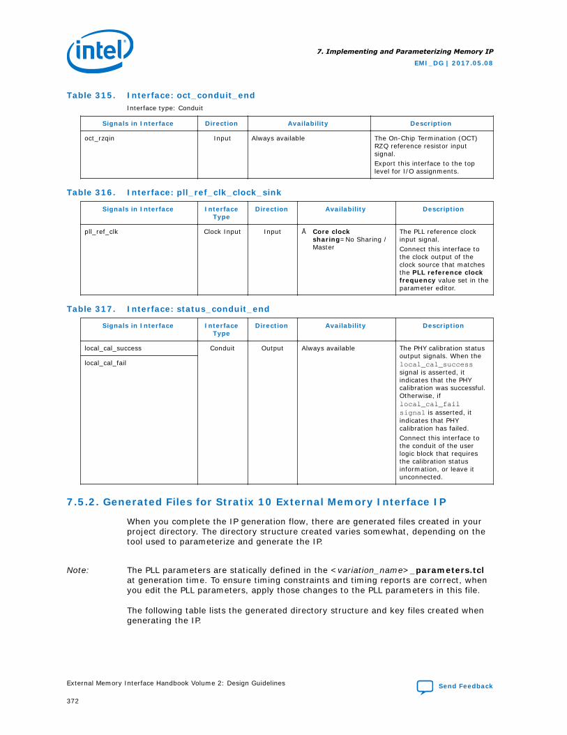
Table 315. Interface: oct_conduit_endInterface type: Conduit
Signals in Interface Direction Availability Description
oct_rzqin Input Always available The On-Chip Termination (OCT)RZQ reference resistor inputsignal.Export this interface to the toplevel for I/O assignments.
Table 316. Interface: pll_ref_clk_clock_sink
Signals in Interface InterfaceType
Direction Availability Description
pll_ref_clk Clock Input Input • Core clocksharing=No Sharing /Master
The PLL reference clockinput signal.Connect this interface tothe clock output of theclock source that matchesthe PLL reference clockfrequency value set in theparameter editor.
Table 317. Interface: status_conduit_end
Signals in Interface InterfaceType
Direction Availability Description
local_cal_success Conduit Output Always available The PHY calibration statusoutput signals. When thelocal_cal_successsignal is asserted, itindicates that the PHYcalibration was successful.Otherwise, iflocal_cal_failsignal is asserted, itindicates that PHYcalibration has failed.Connect this interface tothe conduit of the userlogic block that requiresthe calibration statusinformation, or leave itunconnected.
local_cal_fail
7.5.2. Generated Files for Stratix 10 External Memory Interface IP
When you complete the IP generation flow, there are generated files created in yourproject directory. The directory structure created varies somewhat, depending on thetool used to parameterize and generate the IP.
Note: The PLL parameters are statically defined in the <variation_name>_parameters.tclat generation time. To ensure timing constraints and timing reports are correct, whenyou edit the PLL parameters, apply those changes to the PLL parameters in this file.
The following table lists the generated directory structure and key files created whengenerating the IP.
7. Implementing and Parameterizing Memory IP
EMI_DG | 2017.05.08
External Memory Interface Handbook Volume 2: Design Guidelines Send Feedback
372
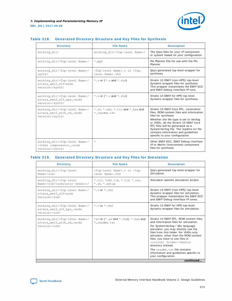
Table 318. Generated Directory Structure and Key Files for Synthesis
Directory File Name Description
working_dir/ working_dir/<Top-level Name>/ The Qsys files for your IP componentor system based on your configuration.
working_dir/<Top-level Name>/ *.ppf Pin Planner File for use with the PinPlanner.
working_dir/<Top-level Name>/synth/
<Top-level Name>.v or <Top-level Name>.vhd
Qsys generated top-level wrapper forsynthesis.
working_dir/<Top-level Name>/altera_emif_S10<acdsversion>/synth/
*.v or (*.v and *.vhd) Stratix 10 EMIF (non-HPS) top-leveldynamic wrapper files for synthesis.This wrapper instantiates the EMIF ECCand EMIF Debug Interface IP core.
working_dir/<Top-level Name>/altera_emif_s10_hps_<acdsversion>/synth/
*.v or (*.v and *.vhd) Stratix 10 EMIF for HPS top-leveldynamic wrapper files for synthesis.
working_dir/<Top-level Name>/altera_emif_arch_nd_<acdsversion>/synth/
*.sv, *.sdc, *.tcl and *.hex and*_readme.txt
Stratix 10 EMIF Core RTL, constraintsfiles, ROM content files and informationfiles for synthesis.Whether the file type is set to Verilogor VHDL, all the Stratix 10 EMIF CoreRTL files will be generated as aSystemVerilog file. The readme.txt filecontains information and guidelinesspecific to your configuration.
working_dir/<Top-level Name>/<other components>_<acdsversion>/synth/
* Other EMIF ECC, EMIF Debug InterfaceIP or Merlin Interconnect componentfiles for synthesis.
Table 319. Generated Directory Structure and Key Files for Simulation
Directory File Name Description
working_dir/<Top-levelName>/sim/
<Top-level Name>.v or <Top-level Name>.vhd
Qsys generated top-level wrapper forsimulation.
working_dir/<Top-levelName>/sim/<simulator vendor>/
*.tcl, *cds.lib, *.lib, *.var,*.sh, *.setup
Simulator-specific simulation scripts.
working_dir/<Top-level Name>/altera_emif_s10<acdsversion>/sim/
*.v or *.vhd Stratix 10 EMIF (non-HPS) top-leveldynamic wrapper files for simulation.This wrapper instantiates the EMIF ECCand EMIF Debug Interface IP cores.
working_dir/<Top-level Name>/altera_emif_s10_hps_<acdsversion>/sim/
*.v or *.vhd Stratix 10 EMIF for HPS top-leveldynamic wrapper files for simulation.
working_dir/<Top-level Name>/altera_emif_arch_nd_<acdsversion>/sim/
*sv or (*.sv and *.vhd), *.hex and*_readme.txt
Stratix 10 EMIF RTL, ROM content files,and information files for simulation.For SystemVerilog / Mix languagesimulator, you may directly use thefiles from this folder. For VHDL-onlysimulator, other than the ROM contentfiles, you have to use files in<current folder>/mentordirectory instead.The readme.txt file containsinformation and guidelines specific toyour configuration.
continued...
7. Implementing and Parameterizing Memory IP
EMI_DG | 2017.05.08
Send Feedback External Memory Interface Handbook Volume 2: Design Guidelines
373
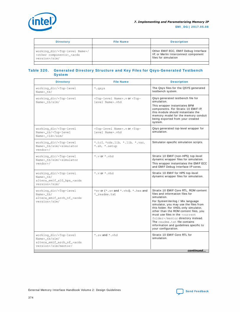
Directory File Name Description
working_dir/<Top-level Name>/<other components>_<acdsversion>/sim/
Other EMIF ECC, EMIF Debug InterfaceIP, or Merlin Interconnect componentfiles for simulation
Table 320. Generated Directory Structure and Key Files for Qsys-Generated TestbenchSystem
Directory File Name Description
working_dir/<Top-levelName>_tb/
*.qsys The Qsys files for the QSYS generatedtestbench system.
working_dir/<Top-levelName>_tb/sim/
<Top-level Name>.v or <Top-level Name>.vhd
Qsys generated testbench file forsimulation.This wrapper instantiates BFMcomponents. For Stratix 10 EMIF IP,this module should instantiate thememory model for the memory conduitbeing exported from your createdsystem.
working_dir/<Top-levelName>_tb/<Top-levelName>_<id>/sim/
<Top-level Name>.v or <Top-level Name>.vhd
Qsys generated top-level wrapper forsimulation.
working_dir/<Top-levelName>_tb/sim/<simulatorvendor>/
*.tcl, *cds.lib, *.lib, *.var,*.sh, *.setup
Simulator-specific simulation scripts.
working_dir/<Top-levelName>_tb/sim/<simulatorvendor>/
*.v or *.vhd Stratix 10 EMIF (non-HPS) top-leveldynamic wrapper files for simulation.This wrapper instantiates the EMIF ECCand EMIF Debug Interface IP cores.
working_dir/<Top-levelName>_tb/altera_emif_a10_hps_<acdsversion>/sim/
*.v or *.vhd Stratix 10 EMIF for HPS top-leveldynamic wrapper files for simulation.
working_dir/<Top-levelName>_tb/altera_emif_arch_nf_<acdsversion>/sim/
*sv or (*.sv and *.vhd), *.hex and*_readme.txt
Stratix 10 EMIF Core RTL, ROM contentfiles and information files forsimulation.For SystemVerilog / Mix languagesimulator, you may use the files fromthis folder. For VHDL-only simulator,other than the ROM content files, youmust use files in the <currentfolder>/mentor directory instead.The readme.txt file containsinformation and guidelines specific toyour configuration.
working_dir/<Top-levelName>_tb/sim/altera_emif_arch_nf_<acdsversion>/sim/mentor/
*.sv and *.vhd Stratix 10 EMIF Core RTL forsimulation.
continued...
7. Implementing and Parameterizing Memory IP
EMI_DG | 2017.05.08
External Memory Interface Handbook Volume 2: Design Guidelines Send Feedback
374
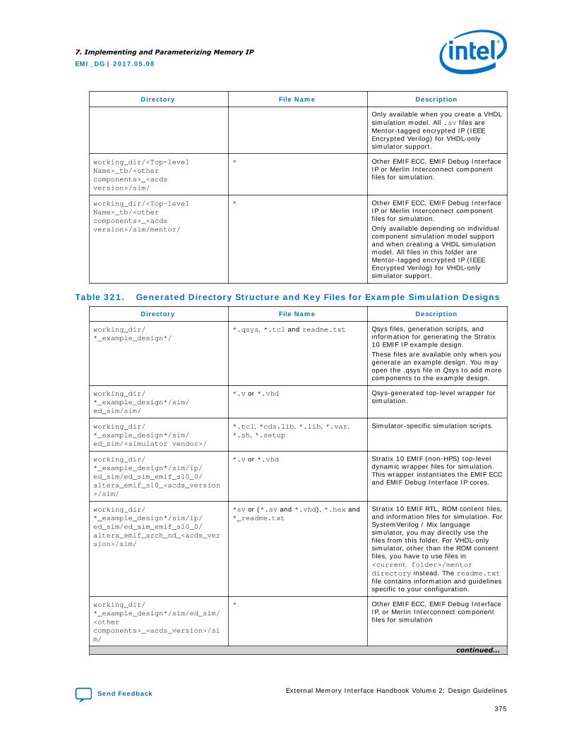
Directory File Name Description
Only available when you create a VHDLsimulation model. All .sv files areMentor-tagged encrypted IP (IEEEEncrypted Verilog) for VHDL-onlysimulator support.
working_dir/<Top-levelName>_tb/<othercomponents>_<acdsversion>/sim/
* Other EMIF ECC, EMIF Debug InterfaceIP or Merlin Interconnect componentfiles for simulation.
working_dir/<Top-levelName>_tb/<othercomponents>_<acdsversion>/sim/mentor/
* Other EMIF ECC, EMIF Debug InterfaceIP or Merlin Interconnect componentfiles for simulation.Only available depending on individualcomponent simulation model supportand when creating a VHDL simulationmodel. All files in this folder areMentor-tagged encrypted IP (IEEEEncrypted Verilog) for VHDL-onlysimulator support.
Table 321. Generated Directory Structure and Key Files for Example Simulation Designs
Directory File Name Description
working_dir/*_example_design*/
*.qsys, *.tcl and readme.txt Qsys files, generation scripts, andinformation for generating the Stratix10 EMIF IP example design.These files are available only when yougenerate an example design. You mayopen the .qsys file in Qsys to add morecomponents to the example design.
working_dir/*_example_design*/sim/ed_sim/sim/
*.v or *.vhd Qsys-generated top-level wrapper forsimulation.
working_dir/*_example_design*/sim/ed_sim/<simulator vendor>/
*.tcl, *cds.lib, *.lib, *.var,*.sh, *.setup
Simulator-specific simulation scripts.
working_dir/*_example_design*/sim/ip/ed_sim/ed_sim_emif_s10_0/altera_emif_s10_<acds_version>/sim/
*.v or *.vhd Stratix 10 EMIF (non-HPS) top-leveldynamic wrapper files for simulation.This wrapper instantiates the EMIF ECCand EMIF Debug Interface IP cores.
working_dir/*_example_design*/sim/ip/ed_sim/ed_sim_emif_s10_0/altera_emif_arch_nd_<acds_version>/sim/
*sv or (*.sv and *.vhd), *.hex and*_readme.txt
Stratix 10 EMIF RTL, ROM content files,and information files for simulation. ForSystemVerilog / Mix languagesimulator, you may directly use thefiles from this folder. For VHDL-onlysimulator, other than the ROM contentfiles, you have to use files in<current folder>/mentordirectory instead. The readme.txtfile contains information and guidelinesspecific to your configuration.
working_dir/*_example_design*/sim/ed_sim/<othercomponents>_<acds_version>/sim/
* Other EMIF ECC, EMIF Debug InterfaceIP, or Merlin Interconnect componentfiles for simulation
continued...
7. Implementing and Parameterizing Memory IP
EMI_DG | 2017.05.08
Send Feedback External Memory Interface Handbook Volume 2: Design Guidelines
375
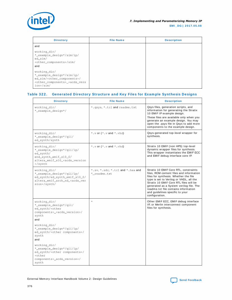
Directory File Name Description
and
working_dir/*_example_design*/sim/ip/ed_sim/<other_components>/sim/
and
working_dir/*_example_design*/sim/ip/ed_sim/<other_components>/<other_components>_<acds_version>/sim/
Table 322. Generated Directory Structure and Key Files for Example Synthesis Designs
Directory File Name Description
working_dir/*_example_design*/
*.qsys, *.tcl and readme.txt Qsys files, generation scripts, andinformation for generating the Stratix10 EMIF IP example design.These files are available only when yougenerate an example design. You mayopen the .qsys file in Qsys to add morecomponents to the example design.
working_dir/*_example_design*/qii/ed_synth/synth
*.v or (*.v and *.vhd) Qsys-generated top-level wrapper forsynthesis.
working_dir/*_example_design*/qii/ip/ed_synth/end_synth_emif_s10_0/altera_emif_s10_<acds_version>/synth
*.v or (*.v and *.vhd) Stratix 10 EMIF (non HPS) top-leveldynamic wrapper files for synthesis.This wrapper instantiates the EMIF ECCand EMIF debug interface core IP.
working_dir/*_example_design*/qii/ip/ed_synth/ed_synth_emif_s10_0/altera_emif_arch_nd_<acds_version>/synth/
*.sv, *.sdc, *.tcl and *.hex and*_readme.txt
Stratix 10 EMIF Core RTL, constraintsfiles, ROM content files and informationfiles for synthesis. Whether the filetype is set to Verilog or VHDL, all theStratix 10 EMIF Core RTL files will begenerated as a System verilog file. Thereadme.txt file contains informationand guidelines specific to yourconfiguration.
working_dir/*_example_design*/qii/ed_synth/<othercomponents>_<acds_version>/synth
and
working_dir/*_example_design*/qii/ip/ed_synth/<other components>/synth
and
working_dir/*_example_design*/qii/ip/ed_synth/<other components>/<othercomponents>_acds_version>/synth
* Other EMIF ECC, EMIF debug interfaceIP, or Merlin interconnect componentfiles for synthesis.
7. Implementing and Parameterizing Memory IP
EMI_DG | 2017.05.08
External Memory Interface Handbook Volume 2: Design Guidelines Send Feedback
376
7.5.3. Stratix 10 EMIF IP DDR4 Parameters
The Stratix 10 EMIF IP parameter editor allows you to parameterize settings for theStratix 10 EMIF IP.
The text window at the bottom of the parameter editor displays information about thememory interface, as well as warning and error messages. You should correct anyerrors indicated in this window before clicking the Finish button.
Note: Default settings are the minimum required to achieve timing, and may vary dependingon memory protocol.
The following tables describe the parameterization settings available in the parametereditor for the Stratix 10 EMIF IP.
7.5.3.1. Stratix 10 EMIF IP DDR4 Parameters: General
Table 323. Group: General / FPGA
Display Name Identifier Description
Speed grade PHY_FPGA_SPEEDGRADE_GUI
Indicates the device speed grade, and whether it is anengineering sample (ES) or production device. This value isbased on the device that you select in the parameter editor.If you do not specify a device, the system assumes adefault value. Ensure that you always specify the correctdevice during IP generation, otherwise your IP may notwork in hardware.
Table 324. Group: General / Interface
Display Name Identifier Description
Configuration PHY_CONFIG_ENUM Specifies the configuration of the memory interface. Theavailable options depend on the protocol in use. Optionsinclude Hard PHY and Hard Controller, Hard PHY and SoftController, or Hard PHY only. If you select Hard PHY only,the AFI interface is exported to allow connection of acustom memory controller or third-party IP.
Instantiate two controllerssharing a Ping Pong PHY
PHY_PING_PONG_EN Specifies the instantiation of two identical memorycontrollers that share an address/command bus through theuse of Ping Pong PHY. This parameter is available only if youspecify the Hard PHY and Hard Controller option. When thisparameter is enabled, the IP exposes two independentAvalon interfaces to the user logic, and a single externalmemory interface with double width for the data bus andthe CS#, CKE, ODT, and CK/CK# signals.
Table 325. Group: General / Clocks
Display Name Identifier Description
Core clocks sharing PHY_CORE_CLKS_SHARING_ENUM
When a design contains multiple interfaces of the sameprotocol, rate, frequency, and PLL reference clock source,they can share a common set of core clock domains. Bysharing core clock domains, they reduce clock networkusage and avoid clock synchronization logic between theinterfaces. To share core clocks, denote one of theinterfaces as "Master", and the remaining interfaces as"Slave". In the RTL, connect the clks_sharing_master_out
continued...
7. Implementing and Parameterizing Memory IP
EMI_DG | 2017.05.08
Send Feedback External Memory Interface Handbook Volume 2: Design Guidelines
377
Display Name Identifier Description
signal from the master interface to theclks_sharing_slave_in signal of all the slave interfaces. Bothmaster and slave interfaces still expose their own outputclock ports in the RTL (for example, emif_usr_clk, afi_clk),but the physical signals are equivalent, hence it does notmatter whether a clock port from a master or a slave isused. As the combined width of all interfaces sharing thesame core clock increases, you may encounter timingclosure difficulty for transfers between the FPGA core andthe periphery.
Use recommended PLLreference clock frequency
PHY_DDR4_DEFAULT_REF_CLK_FREQ
Specifies that the PLL reference clock frequency isautomatically calculated for best performance. If you wantto specify a different PLL reference clock frequency, uncheckthe check box for this parameter.
Memory clock frequency PHY_MEM_CLK_FREQ_MHZ
Specifies the operating frequency of the memory interfacein MHz. If you change the memory frequency, you shouldupdate the memory latency parameters on the "Memory"tab and the memory timing parameters on the "MemTiming" tab.
Clock rate of user logic PHY_RATE_ENUM Specifies the relationship between the user logic clockfrequency and the memory clock frequency. For example, ifthe memory clock sent from the FPGA to the memorydevice is toggling at 800MHz, a quarter-rate interfacemeans that the user logic in the FPGA runs at 200MHz.
PLL reference clock frequency PHY_REF_CLK_FREQ_MHZ
Specifies the PLL reference clock frequency. You mustconfigure this parameter only if you do not check the "Userecommended PLL reference clock frequency" parameter. Toconfigure this parameter, select a valid PLL reference clockfrequency from the list. The values in the list can change ifyou change the memory interface frequency and/or theclock rate of the user logic. For best jitter performance, youshould use the fastest possible PLL reference clockfrequency.
PLL reference clock jitter PHY_REF_CLK_JITTER_PS
Specifies the peak-to-peak jitter on the PLL reference clocksource. The clock source of the PLL reference clock mustmeet or exceed the following jitter requirements: 10ps peakto peak, or 1.42ps RMS at 1e-12 BER, 1.22ps at 1e-16 BER.
Specify additional core clocksbased on existing PLL
PLL_ADD_EXTRA_CLKS
Displays additional parameters allowing you to createadditional output clocks based on the existing PLL. Thisparameter provides an alternative clock-generationmechanism for when your design exhausts available PLLresources. The additional output clocks that you create canbe fed into the core. Clock signals created with thisparameter are synchronous to each other, but asynchronousto the memory interface core clock domains (such asemif_usr_clk or afi_clk). You must follow proper clock-domain-crossing techniques when transferring data betweenclock domains.
Table 326. Group: General / Additional Core Clocks
Display Name Identifier Description
Number of additional coreclocks
PLL_USER_NUM_OF_EXTRA_CLKS
Specifies the number of additional output clocks to createfrom the PLL.
7.5.3.2. Stratix 10 EMIF IP DDR4 Parameters: Memory
7. Implementing and Parameterizing Memory IP
EMI_DG | 2017.05.08
External Memory Interface Handbook Volume 2: Design Guidelines Send Feedback
378
Table 327. Group: Memory / Topology
Display Name Identifier Description
DQS group of ALERT# MEM_DDR4_ALERT_N_DQS_GROUP
Select the DQS group with which the ALERT# pin is placed.
ALERT# pin placement MEM_DDR4_ALERT_N_PLACEMENT_ENUM
Specifies placement for the mem_alert_n signal. If youselect "I/O Lane with Address/Command Pins", you can pickthe I/O lane and pin index in the add/cmd bank with thesubsequent drop down menus. If you select "I/O Lane withDQS Group", you can specify the DQS group with which toplace the mem_alert_n pin. If you select "Automaticallyselect a location", the IP automatically selects a pin for themem_alert_n signal. If you select this option, no additionallocation constraints can be applied to the mem_alert_n pin,or a fitter error will result during compilation. For optimumsignal integrity, you should choose "I/O Lane with Address/Command Pins". For interfaces containing multiple memorydevices, it is recommended to connect the ALERT# pinstogether to the ALERT#pin on the FPGA.
Enable ALERT#/PAR pins MEM_DDR4_ALERT_PAR_EN
Allows address/command calibration, which may providebetter margins on the address/command bus. The alert_nsignal is not accessible in the AFI or Avalon domains. Thismeans there is no way to know whether a parity error hasoccurred during user mode. The parity pin is a dedicated pinin the address/command bank, but the alert_n pin can beplaced in any bank that spans the memory interface. Youshould explicitly choose the location of the alert_n pin andplace it in the address/command bank.
Bank address width MEM_DDR4_BANK_ADDR_WIDTH
Specifies the number of bank address pins. Refer to thedata sheet for your memory device. The density of theselected memory device determines the number of bankaddress pins needed for access to all available banks.
Bank group width MEM_DDR4_BANK_GROUP_WIDTH
Specifies the number of bank group pins. Refer to the datasheet for your memory device. The density of the selectedmemory device determines the number of bank group pinsneeded for access to all available bank groups.
Chip ID width MEM_DDR4_CHIP_ID_WIDTH
Specifies the number of chip ID pins. Only applicable toregistered and load-reduced DIMMs that use 3DS/TSVmemory devices.
Number of clocks MEM_DDR4_CK_WIDTH
Specifies the number of CK/CK# clock pairs exposed by thememory interface. Usually more than 1 pair is required forRDIMM/LRDIMM formats. The value of this parameterdepends on the memory device selected; refer to the datasheet for your memory device.
Column address width MEM_DDR4_COL_ADDR_WIDTH
Specifies the number of column address pins. Refer to thedata sheet for your memory device. The density of theselected memory device determines the number of addresspins needed for access to all available columns.
Number of chip selects perDIMM
MEM_DDR4_CS_PER_DIMM
Specifies the number of chip selects per DIMM.
Number of chip selects MEM_DDR4_DISCRETE_CS_WIDTH
Specifies the total number of chip selects in the interface,up to a maximum of 4. This parameter applies to discretecomponents only.
Data mask MEM_DDR4_DM_EN Indicates whether the interface uses data mask (DM) pins.This feature allows specified portions of the data bus to bewritten to memory (not available in x4 mode). One DM pinexists per DQS group.
continued...
7. Implementing and Parameterizing Memory IP
EMI_DG | 2017.05.08
Send Feedback External Memory Interface Handbook Volume 2: Design Guidelines
379
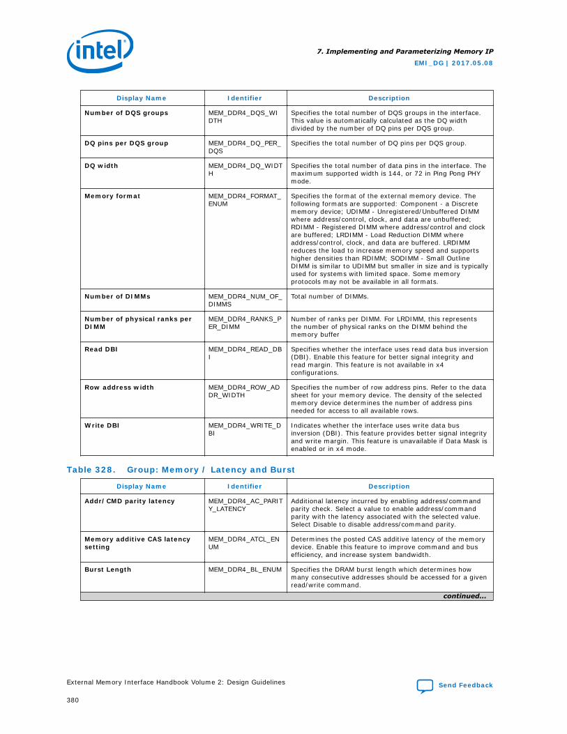
Display Name Identifier Description
Number of DQS groups MEM_DDR4_DQS_WIDTH
Specifies the total number of DQS groups in the interface.This value is automatically calculated as the DQ widthdivided by the number of DQ pins per DQS group.
DQ pins per DQS group MEM_DDR4_DQ_PER_DQS
Specifies the total number of DQ pins per DQS group.
DQ width MEM_DDR4_DQ_WIDTH
Specifies the total number of data pins in the interface. Themaximum supported width is 144, or 72 in Ping Pong PHYmode.
Memory format MEM_DDR4_FORMAT_ENUM
Specifies the format of the external memory device. Thefollowing formats are supported: Component - a Discretememory device; UDIMM - Unregistered/Unbuffered DIMMwhere address/control, clock, and data are unbuffered;RDIMM - Registered DIMM where address/control and clockare buffered; LRDIMM - Load Reduction DIMM whereaddress/control, clock, and data are buffered. LRDIMMreduces the load to increase memory speed and supportshigher densities than RDIMM; SODIMM - Small OutlineDIMM is similar to UDIMM but smaller in size and is typicallyused for systems with limited space. Some memoryprotocols may not be available in all formats.
Number of DIMMs MEM_DDR4_NUM_OF_DIMMS
Total number of DIMMs.
Number of physical ranks perDIMM
MEM_DDR4_RANKS_PER_DIMM
Number of ranks per DIMM. For LRDIMM, this representsthe number of physical ranks on the DIMM behind thememory buffer
Read DBI MEM_DDR4_READ_DBI
Specifies whether the interface uses read data bus inversion(DBI). Enable this feature for better signal integrity andread margin. This feature is not available in x4configurations.
Row address width MEM_DDR4_ROW_ADDR_WIDTH
Specifies the number of row address pins. Refer to the datasheet for your memory device. The density of the selectedmemory device determines the number of address pinsneeded for access to all available rows.
Write DBI MEM_DDR4_WRITE_DBI
Indicates whether the interface uses write data businversion (DBI). This feature provides better signal integrityand write margin. This feature is unavailable if Data Mask isenabled or in x4 mode.
Table 328. Group: Memory / Latency and Burst
Display Name Identifier Description
Addr/CMD parity latency MEM_DDR4_AC_PARITY_LATENCY
Additional latency incurred by enabling address/commandparity check. Select a value to enable address/commandparity with the latency associated with the selected value.Select Disable to disable address/command parity.
Memory additive CAS latencysetting
MEM_DDR4_ATCL_ENUM
Determines the posted CAS additive latency of the memorydevice. Enable this feature to improve command and busefficiency, and increase system bandwidth.
Burst Length MEM_DDR4_BL_ENUM Specifies the DRAM burst length which determines howmany consecutive addresses should be accessed for a givenread/write command.
continued...
7. Implementing and Parameterizing Memory IP
EMI_DG | 2017.05.08
External Memory Interface Handbook Volume 2: Design Guidelines Send Feedback
380
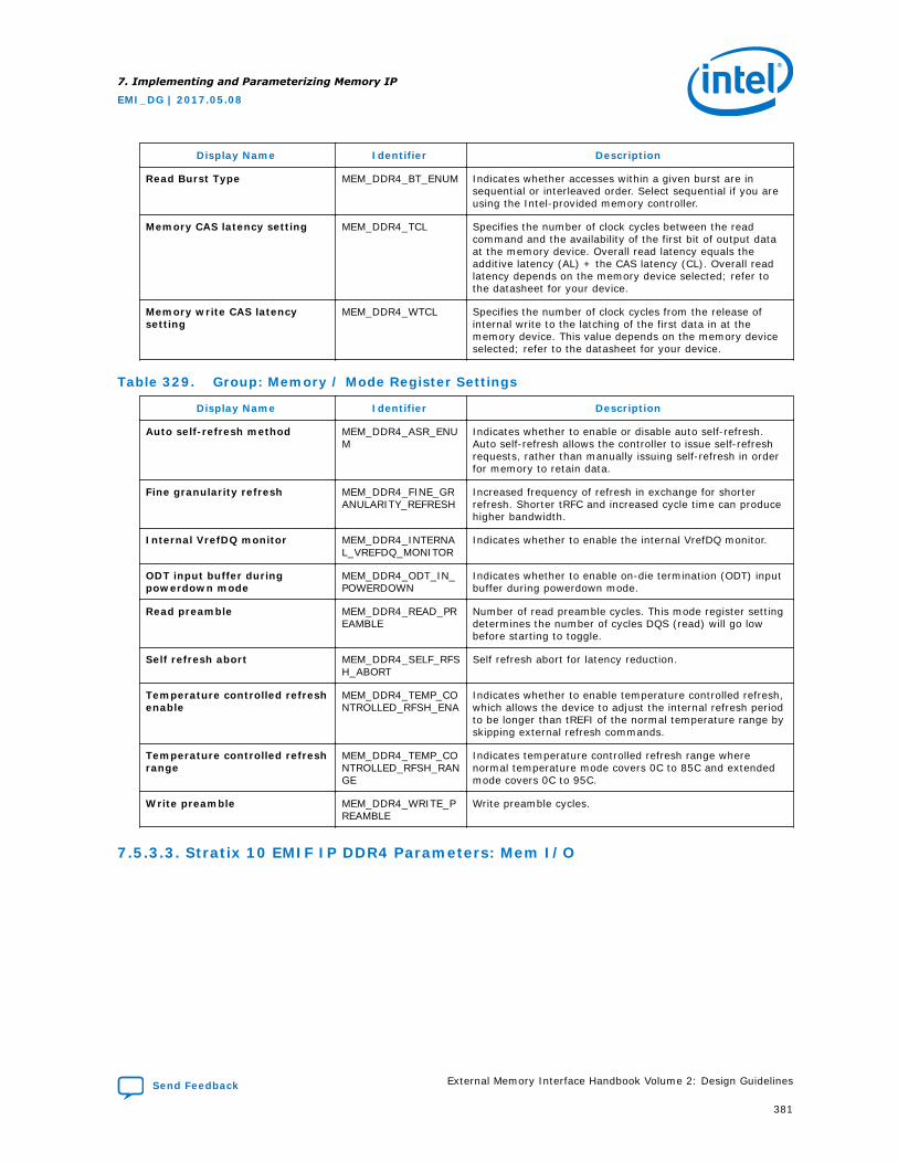
Display Name Identifier Description
Read Burst Type MEM_DDR4_BT_ENUM Indicates whether accesses within a given burst are insequential or interleaved order. Select sequential if you areusing the Intel-provided memory controller.
Memory CAS latency setting MEM_DDR4_TCL Specifies the number of clock cycles between the readcommand and the availability of the first bit of output dataat the memory device. Overall read latency equals theadditive latency (AL) + the CAS latency (CL). Overall readlatency depends on the memory device selected; refer tothe datasheet for your device.
Memory write CAS latencysetting
MEM_DDR4_WTCL Specifies the number of clock cycles from the release ofinternal write to the latching of the first data in at thememory device. This value depends on the memory deviceselected; refer to the datasheet for your device.
Table 329. Group: Memory / Mode Register Settings
Display Name Identifier Description
Auto self-refresh method MEM_DDR4_ASR_ENUM
Indicates whether to enable or disable auto self-refresh.Auto self-refresh allows the controller to issue self-refreshrequests, rather than manually issuing self-refresh in orderfor memory to retain data.
Fine granularity refresh MEM_DDR4_FINE_GRANULARITY_REFRESH
Increased frequency of refresh in exchange for shorterrefresh. Shorter tRFC and increased cycle time can producehigher bandwidth.
Internal VrefDQ monitor MEM_DDR4_INTERNAL_VREFDQ_MONITOR
Indicates whether to enable the internal VrefDQ monitor.
ODT input buffer duringpowerdown mode
MEM_DDR4_ODT_IN_POWERDOWN
Indicates whether to enable on-die termination (ODT) inputbuffer during powerdown mode.
Read preamble MEM_DDR4_READ_PREAMBLE
Number of read preamble cycles. This mode register settingdetermines the number of cycles DQS (read) will go lowbefore starting to toggle.
Self refresh abort MEM_DDR4_SELF_RFSH_ABORT
Self refresh abort for latency reduction.
Temperature controlled refreshenable
MEM_DDR4_TEMP_CONTROLLED_RFSH_ENA
Indicates whether to enable temperature controlled refresh,which allows the device to adjust the internal refresh periodto be longer than tREFI of the normal temperature range byskipping external refresh commands.
Temperature controlled refreshrange
MEM_DDR4_TEMP_CONTROLLED_RFSH_RANGE
Indicates temperature controlled refresh range wherenormal temperature mode covers 0C to 85C and extendedmode covers 0C to 95C.
Write preamble MEM_DDR4_WRITE_PREAMBLE
Write preamble cycles.
7.5.3.3. Stratix 10 EMIF IP DDR4 Parameters: Mem I/O
7. Implementing and Parameterizing Memory IP
EMI_DG | 2017.05.08
Send Feedback External Memory Interface Handbook Volume 2: Design Guidelines
381
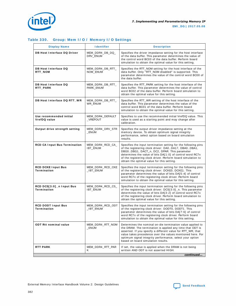
Table 330. Group: Mem I/O / Memory I/O Settings
Display Name Identifier Description
DB Host Interface DQ Driver MEM_DDR4_DB_DQ_DRV_ENUM
Specifies the driver impedance setting for the host interfaceof the data buffer. This parameter determines the value ofthe control word BC03 of the data buffer. Perform boardsimulation to obtain the optimal value for this setting.
DB Host Interface DQRTT_NOM
MEM_DDR4_DB_RTT_NOM_ENUM
Specifies the RTT_NOM setting for the host interface of thedata buffer. Only "RTT_NOM disabled" is supported. Thisparameter determines the value of the control word BC00 ofthe data buffer.
DB Host Interface DQRTT_PARK
MEM_DDR4_DB_RTT_PARK_ENUM
Specifies the RTT_PARK setting for the host interface of thedata buffer. This parameter determines the value of controlword BC02 of the data buffer. Perform board simulation toobtain the optimal value for this setting.
DB Host Interface DQ RTT_WR MEM_DDR4_DB_RTT_WR_ENUM
Specifies the RTT_WR setting of the host interface of thedata buffer. This parameter determines the value of thecontrol word BC01 of the data buffer. Perform boardsimulation to obtain the optimal value for this setting.
Use recommended initialVrefDQ value
MEM_DDR4_DEFAULT_VREFOUT
Specifies to use the recommended initial VrefDQ value. Thisvalue is used as a starting point and may change aftercalibration.
Output drive strength setting MEM_DDR4_DRV_STR_ENUM
Specifies the output driver impedance setting at thememory device. To obtain optimum signal integrityperformance, select option based on board simulationresults.
RCD CA Input Bus Termination MEM_DDR4_RCD_CA_IBT_ENUM
Specifies the input termination setting for the following pinsof the registering clock driver: DA0..DA17, DBA0..DBA1,DBG0..DBG1, DACT_n, DC2, DPAR. This parameterdetermines the value of bits DA[1:0] of control word RC7xof the registering clock driver. Perform board simulation toobtain the optimal value for this setting.
RCD DCKE Input BusTermination
MEM_DDR4_RCD_CKE_IBT_ENUM
Specifies the input termination setting for the following pinsof the registering clock driver: DCKE0, DCKE1. Thisparameter determines the value of bits DA[5:4] of controlword RC7x of the registering clock driver. Perform boardsimulation to obtain the optimal value for this setting.
RCD DCS[3:0]_n Input BusTermination
MEM_DDR4_RCD_CS_IBT_ENUM
Specifies the input termination setting for the following pinsof the registering clock driver: DCS[3:0]_n. This parameterdetermines the value of bits DA[3:2] of control word RC7xof the registering clock driver. Perform board simulation toobtain the optimal value for this setting.
RCD DODT Input BusTermination
MEM_DDR4_RCD_ODT_IBT_ENUM
Specifies the input termination setting for the following pinsof the registering clock driver: DODT0, DODT1. Thisparameter determines the value of bits DA[7:6] of controlword RC7x of the registering clock driver. Perform boardsimulation to obtain the optimal value for this setting.
ODT Rtt nominal value MEM_DDR4_RTT_NOM_ENUM
Determines the nominal on-die termination value applied tothe DRAM. The termination is applied any time that ODT isasserted. If you specify a different value for RTT_WR, thatvalue takes precedence over the values mentioned here. Foroptimum signal integrity performance, select your optionbased on board simulation results.
RTT PARK MEM_DDR4_RTT_PARK
If set, the value is applied when the DRAM is not beingwritten AND ODT is not asserted HIGH.
continued...
7. Implementing and Parameterizing Memory IP
EMI_DG | 2017.05.08
External Memory Interface Handbook Volume 2: Design Guidelines Send Feedback
382
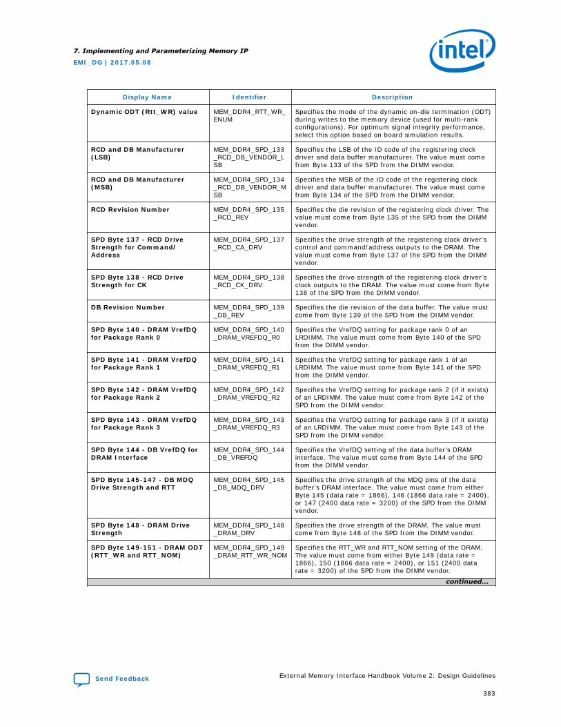
Display Name Identifier Description
Dynamic ODT (Rtt_WR) value MEM_DDR4_RTT_WR_ENUM
Specifies the mode of the dynamic on-die termination (ODT)during writes to the memory device (used for multi-rankconfigurations). For optimum signal integrity performance,select this option based on board simulation results.
RCD and DB Manufacturer(LSB)
MEM_DDR4_SPD_133_RCD_DB_VENDOR_LSB
Specifies the LSB of the ID code of the registering clockdriver and data buffer manufacturer. The value must comefrom Byte 133 of the SPD from the DIMM vendor.
RCD and DB Manufacturer(MSB)
MEM_DDR4_SPD_134_RCD_DB_VENDOR_MSB
Specifies the MSB of the ID code of the registering clockdriver and data buffer manufacturer. The value must comefrom Byte 134 of the SPD from the DIMM vendor.
RCD Revision Number MEM_DDR4_SPD_135_RCD_REV
Specifies the die revision of the registering clock driver. Thevalue must come from Byte 135 of the SPD from the DIMMvendor.
SPD Byte 137 - RCD DriveStrength for Command/Address
MEM_DDR4_SPD_137_RCD_CA_DRV
Specifies the drive strength of the registering clock driver'scontrol and command/address outputs to the DRAM. Thevalue must come from Byte 137 of the SPD from the DIMMvendor.
SPD Byte 138 - RCD DriveStrength for CK
MEM_DDR4_SPD_138_RCD_CK_DRV
Specifies the drive strength of the registering clock driver'sclock outputs to the DRAM. The value must come from Byte138 of the SPD from the DIMM vendor.
DB Revision Number MEM_DDR4_SPD_139_DB_REV
Specifies the die revision of the data buffer. The value mustcome from Byte 139 of the SPD from the DIMM vendor.
SPD Byte 140 - DRAM VrefDQfor Package Rank 0
MEM_DDR4_SPD_140_DRAM_VREFDQ_R0
Specifies the VrefDQ setting for package rank 0 of anLRDIMM. The value must come from Byte 140 of the SPDfrom the DIMM vendor.
SPD Byte 141 - DRAM VrefDQfor Package Rank 1
MEM_DDR4_SPD_141_DRAM_VREFDQ_R1
Specifies the VrefDQ setting for package rank 1 of anLRDIMM. The value must come from Byte 141 of the SPDfrom the DIMM vendor.
SPD Byte 142 - DRAM VrefDQfor Package Rank 2
MEM_DDR4_SPD_142_DRAM_VREFDQ_R2
Specifies the VrefDQ setting for package rank 2 (if it exists)of an LRDIMM. The value must come from Byte 142 of theSPD from the DIMM vendor.
SPD Byte 143 - DRAM VrefDQfor Package Rank 3
MEM_DDR4_SPD_143_DRAM_VREFDQ_R3
Specifies the VrefDQ setting for package rank 3 (if it exists)of an LRDIMM. The value must come from Byte 143 of theSPD from the DIMM vendor.
SPD Byte 144 - DB VrefDQ forDRAM Interface
MEM_DDR4_SPD_144_DB_VREFDQ
Specifies the VrefDQ setting of the data buffer's DRAMinterface. The value must come from Byte 144 of the SPDfrom the DIMM vendor.
SPD Byte 145-147 - DB MDQDrive Strength and RTT
MEM_DDR4_SPD_145_DB_MDQ_DRV
Specifies the drive strength of the MDQ pins of the databuffer's DRAM interface. The value must come from eitherByte 145 (data rate = 1866), 146 (1866 data rate = 2400),or 147 (2400 data rate = 3200) of the SPD from the DIMMvendor.
SPD Byte 148 - DRAM DriveStrength
MEM_DDR4_SPD_148_DRAM_DRV
Specifies the drive strength of the DRAM. The value mustcome from Byte 148 of the SPD from the DIMM vendor.
SPD Byte 149-151 - DRAM ODT(RTT_WR and RTT_NOM)
MEM_DDR4_SPD_149_DRAM_RTT_WR_NOM
Specifies the RTT_WR and RTT_NOM setting of the DRAM.The value must come from either Byte 149 (data rate =1866), 150 (1866 data rate = 2400), or 151 (2400 datarate = 3200) of the SPD from the DIMM vendor.
continued...
7. Implementing and Parameterizing Memory IP
EMI_DG | 2017.05.08
Send Feedback External Memory Interface Handbook Volume 2: Design Guidelines
383
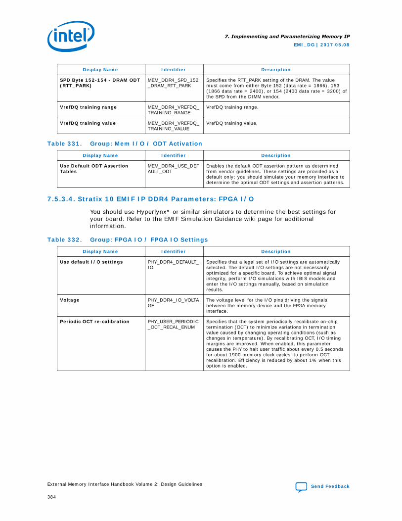
Display Name Identifier Description
SPD Byte 152-154 - DRAM ODT(RTT_PARK)
MEM_DDR4_SPD_152_DRAM_RTT_PARK
Specifies the RTT_PARK setting of the DRAM. The valuemust come from either Byte 152 (data rate = 1866), 153(1866 data rate = 2400), or 154 (2400 data rate = 3200) ofthe SPD from the DIMM vendor.
VrefDQ training range MEM_DDR4_VREFDQ_TRAINING_RANGE
VrefDQ training range.
VrefDQ training value MEM_DDR4_VREFDQ_TRAINING_VALUE
VrefDQ training value.
Table 331. Group: Mem I/O / ODT Activation
Display Name Identifier Description
Use Default ODT AssertionTables
MEM_DDR4_USE_DEFAULT_ODT
Enables the default ODT assertion pattern as determinedfrom vendor guidelines. These settings are provided as adefault only; you should simulate your memory interface todetermine the optimal ODT settings and assertion patterns.
7.5.3.4. Stratix 10 EMIF IP DDR4 Parameters: FPGA I/O
You should use Hyperlynx* or similar simulators to determine the best settings foryour board. Refer to the EMIF Simulation Guidance wiki page for additionalinformation.
Table 332. Group: FPGA IO / FPGA IO Settings
Display Name Identifier Description
Use default I/O settings PHY_DDR4_DEFAULT_IO
Specifies that a legal set of I/O settings are automaticallyselected. The default I/O settings are not necessarilyoptimized for a specific board. To achieve optimal signalintegrity, perform I/O simulations with IBIS models andenter the I/O settings manually, based on simulationresults.
Voltage PHY_DDR4_IO_VOLTAGE
The voltage level for the I/O pins driving the signalsbetween the memory device and the FPGA memoryinterface.
Periodic OCT re-calibration PHY_USER_PERIODIC_OCT_RECAL_ENUM
Specifies that the system periodically recalibrate on-chiptermination (OCT) to minimize variations in terminationvalue caused by changing operating conditions (such aschanges in temperature). By recalibrating OCT, I/O timingmargins are improved. When enabled, this parametercauses the PHY to halt user traffic about every 0.5 secondsfor about 1900 memory clock cycles, to perform OCTrecalibration. Efficiency is reduced by about 1% when thisoption is enabled.
7. Implementing and Parameterizing Memory IP
EMI_DG | 2017.05.08
External Memory Interface Handbook Volume 2: Design Guidelines Send Feedback
384
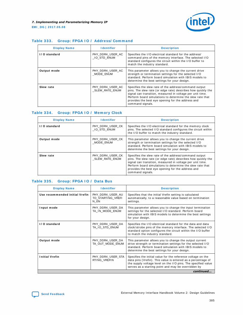
Table 333. Group: FPGA IO / Address/Command
Display Name Identifier Description
I/O standard PHY_DDR4_USER_AC_IO_STD_ENUM
Specifies the I/O electrical standard for the address/command pins of the memory interface. The selected I/Ostandard configures the circuit within the I/O buffer tomatch the industry standard.
Output mode PHY_DDR4_USER_AC_MODE_ENUM
This parameter allows you to change the current drivestrength or termination settings for the selected I/Ostandard. Perform board simulation with IBIS models todetermine the best settings for your design.
Slew rate PHY_DDR4_USER_AC_SLEW_RATE_ENUM
Specifies the slew rate of the address/command outputpins. The slew rate (or edge rate) describes how quickly thesignal can transition, measured in voltage per unit time.Perform board simulations to determine the slew rate thatprovides the best eye opening for the address andcommand signals.
Table 334. Group: FPGA IO / Memory Clock
Display Name Identifier Description
I/O standard PHY_DDR4_USER_CK_IO_STD_ENUM
Specifies the I/O electrical standard for the memory clockpins. The selected I/O standard configures the circuit withinthe I/O buffer to match the industry standard.
Output mode PHY_DDR4_USER_CK_MODE_ENUM
This parameter allows you to change the current drivestrength or termination settings for the selected I/Ostandard. Perform board simulation with IBIS models todetermine the best settings for your design.
Slew rate PHY_DDR4_USER_CK_SLEW_RATE_ENUM
Specifies the slew rate of the address/command outputpins. The slew rate (or edge rate) describes how quickly thesignal can transition, measured in voltage per unit time.Perform board simulations to determine the slew rate thatprovides the best eye opening for the address andcommand signals.
Table 335. Group: FPGA IO / Data Bus
Display Name Identifier Description
Use recommended initial Vrefin PHY_DDR4_USER_AUTO_STARTING_VREFIN_EN
Specifies that the initial Vrefin setting is calculatedautomatically, to a reasonable value based on terminationsettings.
Input mode PHY_DDR4_USER_DATA_IN_MODE_ENUM
This parameter allows you to change the input terminationsettings for the selected I/O standard. Perform boardsimulation with IBIS models to determine the best settingsfor your design.
I/O standard PHY_DDR4_USER_DATA_IO_STD_ENUM
Specifies the I/O electrical standard for the data and dataclock/strobe pins of the memory interface. The selected I/Ostandard option configures the circuit within the I/O bufferto match the industry standard.
Output mode PHY_DDR4_USER_DATA_OUT_MODE_ENUM
This parameter allows you to change the output currentdrive strength or termination settings for the selected I/Ostandard. Perform board simulation with IBIS models todetermine the best settings for your design.
Initial Vrefin PHY_DDR4_USER_STARTING_VREFIN
Specifies the initial value for the reference voltage on thedata pins (Vrefin). This value is entered as a percentage ofthe supply voltage level on the I/O pins. The specified valueserves as a starting point and may be overridden by
continued...
7. Implementing and Parameterizing Memory IP
EMI_DG | 2017.05.08
Send Feedback External Memory Interface Handbook Volume 2: Design Guidelines
385
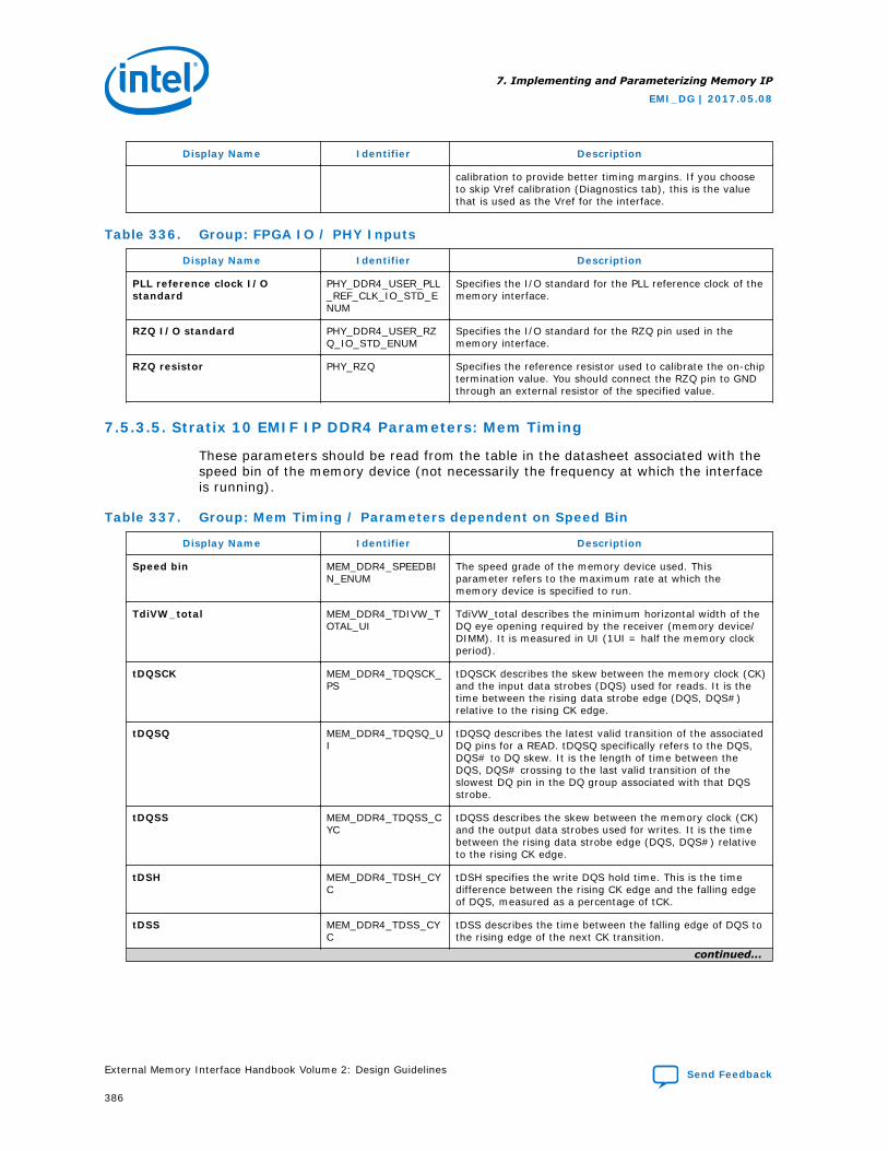
Display Name Identifier Description
calibration to provide better timing margins. If you chooseto skip Vref calibration (Diagnostics tab), this is the valuethat is used as the Vref for the interface.
Table 336. Group: FPGA IO / PHY Inputs
Display Name Identifier Description
PLL reference clock I/Ostandard
PHY_DDR4_USER_PLL_REF_CLK_IO_STD_ENUM
Specifies the I/O standard for the PLL reference clock of thememory interface.
RZQ I/O standard PHY_DDR4_USER_RZQ_IO_STD_ENUM
Specifies the I/O standard for the RZQ pin used in thememory interface.
RZQ resistor PHY_RZQ Specifies the reference resistor used to calibrate the on-chiptermination value. You should connect the RZQ pin to GNDthrough an external resistor of the specified value.
7.5.3.5. Stratix 10 EMIF IP DDR4 Parameters: Mem Timing
These parameters should be read from the table in the datasheet associated with thespeed bin of the memory device (not necessarily the frequency at which the interfaceis running).
Table 337. Group: Mem Timing / Parameters dependent on Speed Bin
Display Name Identifier Description
Speed bin MEM_DDR4_SPEEDBIN_ENUM
The speed grade of the memory device used. Thisparameter refers to the maximum rate at which thememory device is specified to run.
TdiVW_total MEM_DDR4_TDIVW_TOTAL_UI
TdiVW_total describes the minimum horizontal width of theDQ eye opening required by the receiver (memory device/DIMM). It is measured in UI (1UI = half the memory clockperiod).
tDQSCK MEM_DDR4_TDQSCK_PS
tDQSCK describes the skew between the memory clock (CK)and the input data strobes (DQS) used for reads. It is thetime between the rising data strobe edge (DQS, DQS#)relative to the rising CK edge.
tDQSQ MEM_DDR4_TDQSQ_UI
tDQSQ describes the latest valid transition of the associatedDQ pins for a READ. tDQSQ specifically refers to the DQS,DQS# to DQ skew. It is the length of time between theDQS, DQS# crossing to the last valid transition of theslowest DQ pin in the DQ group associated with that DQSstrobe.
tDQSS MEM_DDR4_TDQSS_CYC
tDQSS describes the skew between the memory clock (CK)and the output data strobes used for writes. It is the timebetween the rising data strobe edge (DQS, DQS#) relativeto the rising CK edge.
tDSH MEM_DDR4_TDSH_CYC
tDSH specifies the write DQS hold time. This is the timedifference between the rising CK edge and the falling edgeof DQS, measured as a percentage of tCK.
tDSS MEM_DDR4_TDSS_CYC
tDSS describes the time between the falling edge of DQS tothe rising edge of the next CK transition.
continued...
7. Implementing and Parameterizing Memory IP
EMI_DG | 2017.05.08
External Memory Interface Handbook Volume 2: Design Guidelines Send Feedback
386
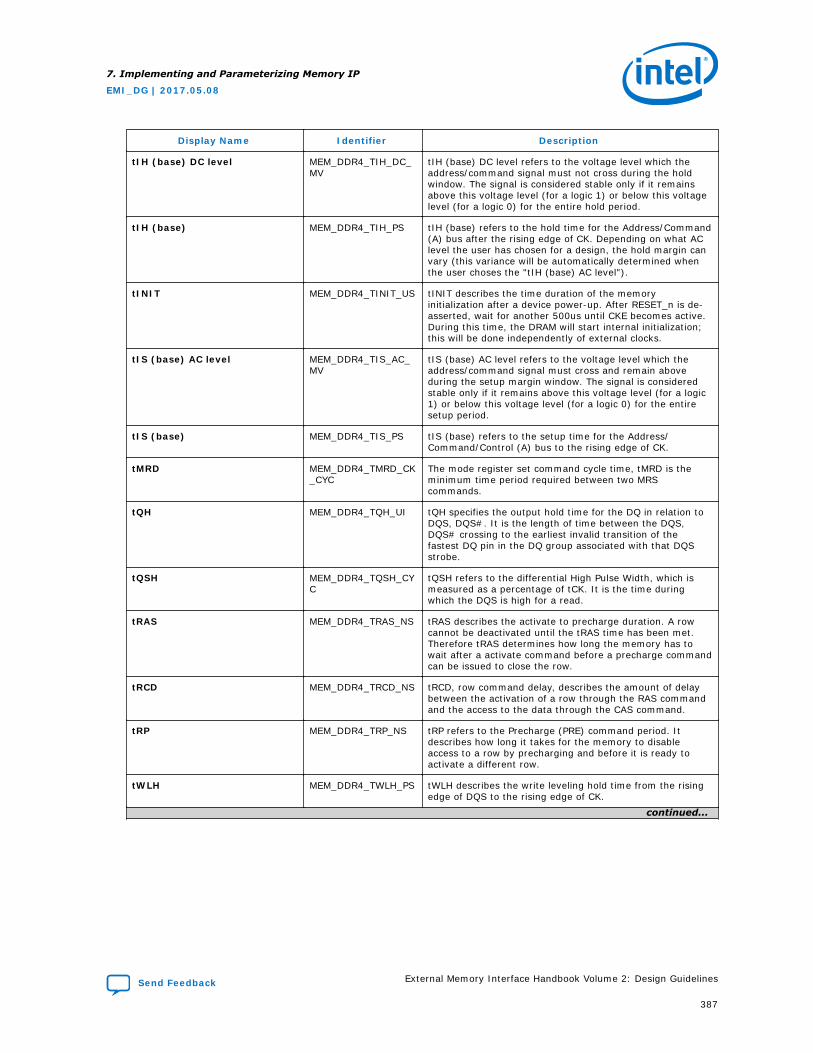
Display Name Identifier Description
tIH (base) DC level MEM_DDR4_TIH_DC_MV
tIH (base) DC level refers to the voltage level which theaddress/command signal must not cross during the holdwindow. The signal is considered stable only if it remainsabove this voltage level (for a logic 1) or below this voltagelevel (for a logic 0) for the entire hold period.
tIH (base) MEM_DDR4_TIH_PS tIH (base) refers to the hold time for the Address/Command(A) bus after the rising edge of CK. Depending on what AClevel the user has chosen for a design, the hold margin canvary (this variance will be automatically determined whenthe user choses the "tIH (base) AC level").
tINIT MEM_DDR4_TINIT_US tINIT describes the time duration of the memoryinitialization after a device power-up. After RESET_n is de-asserted, wait for another 500us until CKE becomes active.During this time, the DRAM will start internal initialization;this will be done independently of external clocks.
tIS (base) AC level MEM_DDR4_TIS_AC_MV
tIS (base) AC level refers to the voltage level which theaddress/command signal must cross and remain aboveduring the setup margin window. The signal is consideredstable only if it remains above this voltage level (for a logic1) or below this voltage level (for a logic 0) for the entiresetup period.
tIS (base) MEM_DDR4_TIS_PS tIS (base) refers to the setup time for the Address/Command/Control (A) bus to the rising edge of CK.
tMRD MEM_DDR4_TMRD_CK_CYC
The mode register set command cycle time, tMRD is theminimum time period required between two MRScommands.
tQH MEM_DDR4_TQH_UI tQH specifies the output hold time for the DQ in relation toDQS, DQS#. It is the length of time between the DQS,DQS# crossing to the earliest invalid transition of thefastest DQ pin in the DQ group associated with that DQSstrobe.
tQSH MEM_DDR4_TQSH_CYC
tQSH refers to the differential High Pulse Width, which ismeasured as a percentage of tCK. It is the time duringwhich the DQS is high for a read.
tRAS MEM_DDR4_TRAS_NS tRAS describes the activate to precharge duration. A rowcannot be deactivated until the tRAS time has been met.Therefore tRAS determines how long the memory has towait after a activate command before a precharge commandcan be issued to close the row.
tRCD MEM_DDR4_TRCD_NS tRCD, row command delay, describes the amount of delaybetween the activation of a row through the RAS commandand the access to the data through the CAS command.
tRP MEM_DDR4_TRP_NS tRP refers to the Precharge (PRE) command period. Itdescribes how long it takes for the memory to disableaccess to a row by precharging and before it is ready toactivate a different row.
tWLH MEM_DDR4_TWLH_PS tWLH describes the write leveling hold time from the risingedge of DQS to the rising edge of CK.
continued...
7. Implementing and Parameterizing Memory IP
EMI_DG | 2017.05.08
Send Feedback External Memory Interface Handbook Volume 2: Design Guidelines
387
Display Name Identifier Description
tWLS MEM_DDR4_TWLS_PS tWLS describes the write leveling setup time. It is measuredfrom the rising edge of CK to the rising edge of DQS.
tWR MEM_DDR4_TWR_NS tWR refers to the Write Recovery time. It specifies theamount of clock cycles needed to complete a write before aprecharge command can be issued.
VdiVW_total MEM_DDR4_VDIVW_TOTAL
VdiVW_total describes the Rx Mask voltage, or the minimumvertical width of the DQ eye opening required by thereceiver (memory device/DIMM). It is measured mV.
Table 338. Group: Mem Timing / Parameters dependent on Speed Bin, OperatingFrequency, and Page Size
Display Name Identifier Description
tCCD_L MEM_DDR4_TCCD_L_CYC
tCCD_L refers to the CAS_n-to-CAS_n delay (long). It is theminimum time interval between two read/write (CAS)commands to the same bank group.
tCCD_S MEM_DDR4_TCCD_S_CYC
tCCD_S refers to the CAS_n-to-CAS_n delay (short). It isthe minimum time interval between two read/write (CAS)commands to different bank groups.
tFAW_dlr MEM_DDR4_TFAW_DLR_CYC
tFAW_dlr refers to the four activate window to differentlogical ranks. It describes the period of time during whichonly four banks can be active across all logical ranks withina 3DS DDR4 device.
tFAW MEM_DDR4_TFAW_NS tFAW refers to the four activate window time. It describesthe period of time during which only four banks can beactive.
tRRD_dlr MEM_DDR4_TRRD_DLR_CYC
tRRD_dlr refers to the Activate to Activate Command Periodto Different Logical Ranks. It is the minimum time interval(measured in memory clock cycles) between two activatecommands to different logical ranks within a 3DS DDR4device.
tRRD_L MEM_DDR4_TRRD_L_CYC
tRRD_L refers to the Activate to Activate Command Period(long). It is the minimum time interval (measured inmemory clock cycles) between two activate commands tothe same bank group.
tRRD_S MEM_DDR4_TRRD_S_CYC
tRRD_S refers to the Activate to Activate Command Period(short). It is the minimum time interval between twoactivate commands to the different bank groups.
tRTP MEM_DDR4_TRTP_CYC
tRTP refers to the internal READ Command to PRECHARGECommand delay. It is the number of memory clock cyclesthat is needed between a read command and a prechargecommand to the same rank.
tWTR_L MEM_DDR4_TWTR_L_CYC
tWTR_L or Write Timing Parameter describes the delay fromstart of internal write transaction to internal read command,for accesses to the same bank group. The delay ismeasured from the first rising memory clock edge after thelast write data is received to the rising memory clock edgewhen a read command is received.
tWTR_S MEM_DDR4_TWTR_S_CYC
tWTR_S or Write Timing Parameter describes the delay fromstart of internal write transaction to internal read command,for accesses to the different bank group. The delay ismeasured from the first rising memory clock edge after thelast write data is received to the rising memory clock edgewhen a read command is received.
7. Implementing and Parameterizing Memory IP
EMI_DG | 2017.05.08
External Memory Interface Handbook Volume 2: Design Guidelines Send Feedback
388
Table 339. Group: Mem Timing / Parameters dependent on Density and Temperature
Display Name Identifier Description
tREFI MEM_DDR4_TREFI_US tREFI refers to the average periodic refresh interval. It isthe maximum amount of time the memory can tolerate inbetween each refresh command
tRFC_dlr MEM_DDR4_TRFC_DLR_NS
tRFC_dlr refers to the Refresh Cycle Time to different logicalrank. It is the amount of delay after a refresh command toone logical rank before an activate command can beaccepted by another logical rank within a 3DS DDR4 device.This parameter is dependent on the memory density and isnecessary for proper hardware functionality.
tRFC MEM_DDR4_TRFC_NS tRFC refers to the Refresh Cycle Time. It is the amount ofdelay after a refresh command before an activate commandcan be accepted by the memory. This parameter isdependent on the memory density and is necessary forproper hardware functionality.
7.5.3.6. Stratix 10 EMIF IP DDR4 Parameters: Board
Table 340. Group: Board / Intersymbol Interference/Crosstalk
Display Name Identifier Description
Address and command ISI/crosstalk
BOARD_DDR4_USER_AC_ISI_NS
The address and command window reduction due to ISI andcrosstalk effects. The number to be entered is the total lossof margin on both the setup and hold sides (measured losson the setup side + measured loss on the hold side). Referto the EMIF Simulation Guidance wiki page for additionalinformation.
Read DQS/DQS# ISI/crosstalk BOARD_DDR4_USER_RCLK_ISI_NS
The reduction of the read data window due to ISI andcrosstalk effects on the DQS/DQS# signal when driven bythe memory device during a read. The number to beentered is the total loss of margin on the setup and holdsides (measured loss on the setup side + measured loss onthe hold side). Refer to the EMIF Simulation Guidance wikipage for additional information.
Read DQ ISI/crosstalk BOARD_DDR4_USER_RDATA_ISI_NS
The reduction of the read data window due to ISI andcrosstalk effects on the DQ signal when driven by thememory device during a read. The number to be entered isthe total loss of margin on the setup and hold side(measured loss on the setup side + measured loss on thehold side). Refer to the EMIF Simulation Guidance wiki pagefor additional information.
Write DQS/DQS# ISI/crosstalk BOARD_DDR4_USER_WCLK_ISI_NS
The reduction of the write data window due to ISI andcrosstalk effects on the DQS/DQS# signal when driven bythe FPGA during a write. The number to be entered is thetotal loss of margin on the setup and hold sides (measuredloss on the setup side + measured loss on the hold side).Refer to the EMIF Simulation Guidance wiki page foradditional information.
Write DQ ISI/crosstalk BOARD_DDR4_USER_WDATA_ISI_NS
The reduction of the write data window due to ISI andcrosstalk effects on the DQ signal when driven by the FPGAduring a write. The number to be entered is the total loss ofmargin on the setup and hold sides (measured loss on the
continued...
7. Implementing and Parameterizing Memory IP
EMI_DG | 2017.05.08
Send Feedback External Memory Interface Handbook Volume 2: Design Guidelines
389
Display Name Identifier Description
setup side + measured loss on the hold side). Refer to theEMIF Simulation Guidance wiki page for additionalinformation.
Use default ISI/crosstalkvalues
BOARD_DDR4_USE_DEFAULT_ISI_VALUES
You can enable this option to use default intersymbolinterference and crosstalk values for your topology. Notethat the default values are not optimized for your board. Foroptimal signal integrity, it is recommended that you do notenable this parameter, but instead perform I/O simulationusing IBIS models and Hyperlynx*, and manually entervalues based on your simulation results, instead of usingthe default values.
Table 341. Group: Board / Board and Package Skews
Display Name Identifier Description
Average delay differencebetween address/commandand CK
BOARD_DDR4_AC_TO_CK_SKEW_NS
The average delay difference between the address/command signals and the CK signal, calculated by averagingthe longest and smallest address/command signal tracedelay minus the maximum CK trace delay. Positive valuesrepresent address and command signals that are longerthan CK signals and negative values represent address andcommand signals that are shorter than CK signals.
Maximum board skew withinaddress/command bus
BOARD_DDR4_BRD_SKEW_WITHIN_AC_NS
The largest skew between the address and commandsignals.
Maximum board skew withinDQS group
BOARD_DDR4_BRD_SKEW_WITHIN_DQS_NS
The largest skew between all DQ and DM pins in a DQSgroup. This value affects the read capture and writemargins.
Average delay differencebetween DQS and CK
BOARD_DDR4_DQS_TO_CK_SKEW_NS
The average delay difference between the DQS signals andthe CK signal, calculated by averaging the longest andsmallest DQS trace delay minus the CK trace delay. Positivevalues represent DQS signals that are longer than CKsignals and negative values represent DQS signals that areshorter than CK signals.
Package deskewed with boardlayout (address/commandbus)
BOARD_DDR4_IS_SKEW_WITHIN_AC_DESKEWED
Enable this parameter if you are compensating for packageskew on the address, command, control, and memory clockbuses in the board layout. Include package skew incalculating the following board skew parameters.
Package deskewed with boardlayout (DQS group)
BOARD_DDR4_IS_SKEW_WITHIN_DQS_DESKEWED
Enable this parameter if you are compensating for packageskew on the DQ, DQS, and DM buses in the board layout.Include package skew in calculating the following boardskew parameters.
Maximum CK delay to DIMM/device
BOARD_DDR4_MAX_CK_DELAY_NS
The delay of the longest CK trace from the FPGA to anyDIMM/device.
Maximum DQS delay to DIMM/device
BOARD_DDR4_MAX_DQS_DELAY_NS
The delay of the longest DQS trace from the FPGA to anyDIMM/device
Maximum delay differencebetween DIMMs/devices
BOARD_DDR4_SKEW_BETWEEN_DIMMS_NS
The largest propagation delay on DQ signals between ranks(applicable only when there is more than one rank). Forexample: when you configure two ranks using one DIMMthere is a short distance between the ranks for the same DQpin; when you implement two ranks using two DIMMs thedistance is larger.
Maximum skew between DQSgroups
BOARD_DDR4_SKEW_BETWEEN_DQS_NS
The largest skew between DQS signals.
7.5.3.7. Stratix 10 EMIF IP DDR4 Parameters: Controller
7. Implementing and Parameterizing Memory IP
EMI_DG | 2017.05.08
External Memory Interface Handbook Volume 2: Design Guidelines Send Feedback
390
Table 342. Group: Controller / Low Power Mode
Display Name Identifier Description
Auto Power-Down Cycles CTRL_DDR4_AUTO_POWER_DOWN_CYCS
Specifies the number of idle controller cycles after which thememory device is placed into power-down mode. You canconfigure the idle waiting time. The supported range fornumber of cycles is from 1 to 65534.
Enable Auto Power-Down CTRL_DDR4_AUTO_POWER_DOWN_EN
Enable this parameter to have the controller automaticallyplace the memory device into power-down mode after aspecified number of idle controller clock cycles. The idle waittime is configurable. All ranks must be idle to enter autopower-down.
Table 343. Group: Controller / Efficiency
Display Name Identifier Description
Address Ordering CTRL_DDR4_ADDR_ORDER_ENUM
Controls the mapping between Avalon addresses andmemory device addresses. By changing the value of thisparameter, you can change the mappings between theAvalon-MM address and the DRAM address. (CS = chipselect, CID = chip ID in 3DS/TSV devices, BG = bank groupaddress, Bank = bank address, Row = row address, Col =column address)
Enable Auto-Precharge Control CTRL_DDR4_AUTO_PRECHARGE_EN
Select this parameter to enable the auto-precharge controlon the controller top level. If you assert the auto-prechargecontrol signal while requesting a read or write burst, youcan specify whether the controller should close (auto-precharge) the currently open page at the end of the reador write burst, potentially making a future access to adifferent page of the same bank faster.
Enable Reordering CTRL_DDR4_REORDER_EN
Enable this parameter to allow the controller to performcommand and data reordering. Reordering can improveefficiency by reducing bus turnaround time and row/bankswitching time. Data reordering allows the single-portmemory controller to change the order of read and writecommands to achieve highest efficiency. Commandreordering allows the controller to issue bank managementcommands early based on incoming patterns, so that thedesired row in memory is already open when the commandreaches the memory interface. For more information, referto the Data Reordering topic in the EMIF Handbook.
Starvation limit for eachcommand
CTRL_DDR4_STARVE_LIMIT
Specifies the number of commands that can be servedbefore a waiting command is served. The controller employsa counter to ensure that all requests are served after a pre-defined interval -- this ensures that low priority requests arenot ignored, when doing data reordering for efficiency. Thevalid range for this parameter is from 1 to 63. For moreinformation, refer to the Starvation Control topic in the EMIFHandbook.
Enable Command PriorityControl
CTRL_DDR4_USER_PRIORITY_EN
Select this parameter to enable user-requested commandpriority control on the controller top level. This parameterinstructs the controller to treat a read or write request ashigh-priority. The controller attempts to fill high-priorityrequests sooner, to reduce latency. Connect this interface tothe conduit of your logic block that determines when theexternal memory interface IP treats the read or writerequest as a high-priority command.
7. Implementing and Parameterizing Memory IP
EMI_DG | 2017.05.08
Send Feedback External Memory Interface Handbook Volume 2: Design Guidelines
391
Table 344. Group: Controller / Configuration, Status, and Error Handling
Display Name Identifier Description
Enable Auto Error Correction CTRL_DDR4_ECC_AUTO_CORRECTION_EN
Specifies that the controller perform auto correction when asingle-bit error is detected by the ECC logic.
Enable Error Detection andCorrection Logic with ECC
CTRL_DDR4_ECC_EN Enables error-correction code (ECC) for single-bit errorcorrection and double-bit error detection. Your memoryinterface must have a width of 16, 24, 40, or 72 bits to useECC. ECC is implemented as soft logic.
Enable Memory-MappedConfiguration and StatusRegister (MMR) Interface
CTRL_DDR4_MMR_EN Enable this parameter to change or read memory timingparameters, memory address size, mode register settings,controller status, and request sideband operations.
Table 345. Group: Controller / Data Bus Turnaround Time
Display Name Identifier Description
Additional read-to-readturnaround time (differentranks)
CTRL_DDR4_RD_TO_RD_DIFF_CHIP_DELTA_CYCS
Specifies additional number of idle controller (not DRAM)cycles when switching the data bus from a read of onelogical rank to a read of another logical rank. This canresolve bus contention problems specific to your boardtopology. The value is added to the default which iscalculated automatically. Use the default setting unless yoususpect a problem exists.
Additional read-to-writeturnaround time (differentranks)
CTRL_DDR4_RD_TO_WR_DIFF_CHIP_DELTA_CYCS
Specifies additional number of idle controller (not DRAM)cycles when switching the data bus from a read of onelogical rank to a write of another logical rank. This can helpresolve bus contention problems specific to your boardtopology. The value is added to the default which iscalculated automatically. Use the default setting unless yoususpect a problem exists.
Additional read-to-writeturnaround time (same rank)
CTRL_DDR4_RD_TO_WR_SAME_CHIP_DELTA_CYCS
Specifies additional number of idle controller (not DRAM)cycles when switching the data bus from a read to a writewithin the same logical rank. This can help resolve buscontention problems specific to your board topology. Thevalue is added to the default which is calculatedautomatically. Use the default setting unless you suspect aproblem exists.
Additional write-to-readturnaround time (differentranks)
CTRL_DDR4_WR_TO_RD_DIFF_CHIP_DELTA_CYCS
Specifies additional number of idle controller (not DRAM)cycles when switching the data bus from a write of onelogical rank to a read of another logical rank. This can helpresolve bus contention problems specific to your boardtopology. The value is added to the default which iscalculated automatically. Use the default setting unless yoususpect a problem exists.
Additional write-to-readturnaround time (same rank)
CTRL_DDR4_WR_TO_RD_SAME_CHIP_DELTA_CYCS
Specifies additional number of idle controller (not DRAM)cycles when switching the data bus from a write to a readwithin the same logical rank. This can help resolve buscontention problems specific to your board topology. Thevalue is added to the default which is calculatedautomatically. Use the default setting unless you suspect aproblem exists.
Additional write-to-writeturnaround time (differentranks)
CTRL_DDR4_WR_TO_WR_DIFF_CHIP_DELTA_CYCS
Specifies additional number of idle controller (not DRAM)cycles when switching the data bus from a write of onelogical rank to a write of another logical rank. This can helpresolve bus contention problems specific to your boardtopology. The value is added to the default which iscalculated automatically. Use the default setting unless yoususpect a problem exists.
7. Implementing and Parameterizing Memory IP
EMI_DG | 2017.05.08
External Memory Interface Handbook Volume 2: Design Guidelines Send Feedback
392
7.5.3.8. Stratix 10 EMIF IP DDR4 Parameters: Diagnostics
Table 346. Group: Diagnostics / Simulation Options
Display Name Identifier Description
Abstract phy for fast simulation DIAG_DDR4_ABSTRACT_PHY
Specifies that the system use Abstract PHY for simulation.Abstract PHY replaces the PHY with a model for fastsimulation and can reduce simulation time by 2-3 times.Abstract PHY is available for certain protocols and devicefamilies, and only when you select Skip Calibration.
Calibration mode DIAG_SIM_CAL_MODE_ENUM
Specifies whether to skip memory interface calibrationduring simulation, or to simulate the full calibration process.Simulating the full calibration process can take hours (oreven days), depending on the width and depth of thememory interface. You can achieve much faster simulationtimes by skipping the calibration process, but that is onlyexpected to work when the memory model is ideal and theinterconnect delays are zero. If you enable this parameter,the interface still performs some memory initializationbefore starting normal operations. Abstract PHY issupported with skip calibration.
Table 347. Group: Diagnostics / Calibration Debug Options
Display Name Identifier Description
Skip address/commanddeskew calibration
DIAG_DDR4_SKIP_CA_DESKEW
Specifies to skip the address/command deskew calibrationstage. Address/command deskew performs per-bit deskewfor the address and command pins.
Skip address/commandleveling calibration
DIAG_DDR4_SKIP_CA_LEVEL
Specifies to skip the address/command leveling stageduring calibration. Address/command leveling attempts tocenter the memory clock edge against CS# by adjustingdelay elements inside the PHY, and then applying the samedelay offset to the rest of the address and command pins.
Skip VREF calibration DIAG_DDR4_SKIP_VREF_CAL
Specifies to skip the VREF stage of calibration. Enable thisparameter for debug purposes only; generally, you shouldinclude the VREF calibration stage during normal operation.
Enable Daisy-Chaining forQuartus Prime EMIF DebugToolkit/On-Chip Debug Port
DIAG_EXPORT_SEQ_AVALON_MASTER
Specifies that the IP export an Avalon-MM master interface(cal_debug_out) which can connect to the cal_debuginterface of other EMIF cores residing in the same I/Ocolumn. This parameter applies only if the EMIF DebugToolkit or On-Chip Debug Port is enabled. Refer to theDebugging Multiple EMIFs wiki page for more informationabout debugging multiple EMIFs.
Quartus Prime EMIF DebugToolkit/On-Chip Debug Port
DIAG_EXPORT_SEQ_AVALON_SLAVE
Specifies the connectivity of an Avalon slave interface foruse by the Quartus Prime EMIF Debug Toolkit or user corelogic. If you set this parameter to "Disabled," no debugfeatures are enabled. If you set this parameter to "Export,"an Avalon slave interface named "cal_debug" is exportedfrom the IP. To use this interface with the EMIF DebugToolkit, you must instantiate and connect an EMIF debuginterface IP core to it, or connect it to the cal_debug_outinterface of another EMIF core. If you select "Add EMIFDebug Interface", an EMIF debug interface componentcontaining a JTAG Avalon Master is connected to the debugport, allowing the core to be accessed by the EMIF DebugToolkit. Only one EMIF debug interface should beinstantiated per I/O column. You can chain additional EMIFor PHYLite cores to the first by enabling the "Enable Daisy-Chaining for Quartus Prime EMIF Debug Toolkit/On-Chip
continued...
7. Implementing and Parameterizing Memory IP
EMI_DG | 2017.05.08
Send Feedback External Memory Interface Handbook Volume 2: Design Guidelines
393
Display Name Identifier Description
Debug Port" option for all cores in the chain, and selecting"Export" for the "Quartus Prime EMIF Debug Toolkit/On-ChipDebug Port" option on all cores after the first.
Interface ID DIAG_INTERFACE_ID Identifies interfaces within the I/O column, for use by theEMIF Debug Toolkit and the On-Chip Debug Port. InterfaceIDs should be unique among EMIF cores within the sameI/O column. If the Quartus Prime EMIF Debug Toolkit/On-Chip Debug Port parameter is set to Disabled, the interfaceID is unused.
Use Soft NIOS Processor forOn-Chip Debug
DIAG_SOFT_NIOS_MODE
Enables a soft Nios processor as a peripheral component toaccess the On-Chip Debug Port. Only one interface in acolumn can activate this option.
Table 348. Group: Diagnostics / Example Design
Display Name Identifier Description
Enable In-System-Sources-and-Probes
DIAG_EX_DESIGN_ISSP_EN
Enables In-System-Sources-and-Probes in the exampledesign for common debug signals, such as calibration statusor example traffic generator per-bit status. This parametermust be enabled if you want to do driver margining.
Number of core clocks sharingslaves to instantiate in theexample design
DIAG_EX_DESIGN_NUM_OF_SLAVES
Specifies the number of core clock sharing slaves toinstantiate in the example design. This parameter appliesonly if you set the "Core clocks sharing" parameter in the"General" tab to Master or Slave.
Table 349. Group: Diagnostics / Traffic Generator
Display Name Identifier Description
Bypass the default trafficpattern
DIAG_BYPASS_DEFAULT_PATTERN
Specifies that the controller/interface bypass the trafficgenerator 2.0 default pattern after reset. If you do notenable this parameter, the traffic generator does not asserta pass or fail status until the generator is configured andsignaled to start by its Avalon configuration interface.
Bypass the traffic generatorrepeated-writes/repeated-reads test pattern
DIAG_BYPASS_REPEAT_STAGE
Specifies that the controller/interface bypass the trafficgenerator's repeat test stage. If you do not enable thisparameter, every write and read is repeated several times.
Bypass the traffic generatorstress pattern
DIAG_BYPASS_STRESS_STAGE
Specifies that the controller/interface bypass the trafficgenerator's stress pattern stage. (Stress patterns are meantto create worst-case signal integrity patterns on the datapins.) If you do not enable this parameter, the trafficgenerator does not assert a pass or fail status until thegenerator is configured and signaled to start by its Avalonconfiguration interface.
Bypass the user-configuredtraffic stage
DIAG_BYPASS_USER_STAGE
Specifies that the controller/interface bypass the user-configured traffic generator's pattern after reset. If you donot enable this parameter, the traffic generator does notassert a pass or fail status until the generator is configuredand signaled to start by its Avalon configuration interface.Configuration can be done by connecting to the trafficgenerator via the EMIF Debug Toolkit, or by using customlogic connected to the Avalon-MM configuration slave porton the traffic generator. Configuration can also be simulatedusing the example testbench provided in thealtera_emif_avl_tg_2_tb.sv file.
continued...
7. Implementing and Parameterizing Memory IP
EMI_DG | 2017.05.08
External Memory Interface Handbook Volume 2: Design Guidelines Send Feedback
394
Display Name Identifier Description
Run diagnostic on infinite testduration
DIAG_INFI_TG2_ERR_TEST
Specifies that the traffic generator run indefinitely until thefirst error is detected.
Export Traffic Generator 2.0configuration interface
DIAG_TG_AVL_2_EXPORT_CFG_INTERFACE
Specifies that the IP export an Avalon-MM slave port forconfiguring the Traffic Generator. This is required only if youare configuring the traffic generator through user logic andnot through through the EMIF Debug Toolkit.
Use configurable Avalon trafficgenerator 2.0
DIAG_USE_TG_AVL_2 This option allows users to add the new configurable Avalontraffic generator to the example design.
Table 350. Group: Diagnostics / Performance
Display Name Identifier Description
Enable Efficiency Monitor DIAG_EFFICIENCY_MONITOR
Adds an Efficiency Monitor component to the Avalon-MMinterface of the memory controller, allowing you to viewefficiency statistics of the interface. You can access theefficiency statistics using the EMIF Debug Toolkit.
Table 351. Group: Diagnostics / Miscellaneous
Display Name Identifier Description
Use short Qsys interface names SHORT_QSYS_INTERFACE_NAMES
Specifies the use of short interface names, for improvedusability and consistency with other Qsys components. Ifthis parameter is disabled, the names of Qsys interfacesexposed by the IP will include the type and direction of theinterface. Long interface names are supported forbackward-compatibility and will be removed in a futurerelease.
7.5.3.9. Stratix 10 EMIF IP DDR4 Parameters: Example Designs
Table 352. Group: Example Designs / Available Example Designs
Display Name Identifier Description
Select design EX_DESIGN_GUI_DDR4_SEL_DESIGN
Specifies the creation of a full Quartus Prime project,instantiating an external memory interface and an exampletraffic generator, according to your parameterization. Afterthe design is created, you can specify the target device andpin location assignments, run a full compilation, verifytiming closure, and test the interface on your board usingthe programming file created by the Quartus Primeassembler. The 'Generate Example Design' button lets yougenerate simulation or synthesis file sets.
Table 353. Group: Example Designs / Example Design Files
Display Name Identifier Description
Simulation EX_DESIGN_GUI_DDR4_GEN_SIM
Specifies that the 'Generate Example Design' button createall necessary file sets for simulation. Expect a shortadditional delay as the file set is created. If you do notenable this parameter, simulation file sets are not created.Instead, the output directory will contain the ed_sim.qsysfile which holds Qsys details of the simulation exampledesign, and a make_sim_design.tcl file with othercorresponding tcl files. You can run make_sim_design.tcl
continued...
7. Implementing and Parameterizing Memory IP
EMI_DG | 2017.05.08
Send Feedback External Memory Interface Handbook Volume 2: Design Guidelines
395
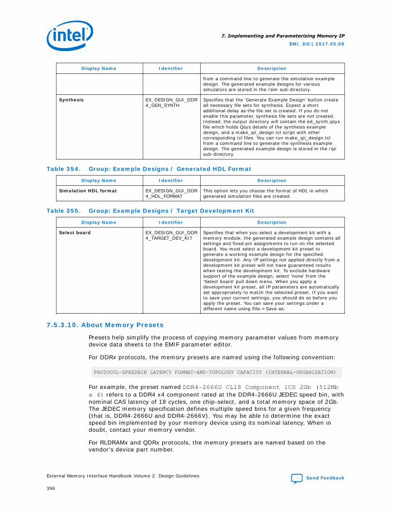
Display Name Identifier Description
from a command line to generate the simulation exampledesign. The generated example designs for varioussimulators are stored in the /sim sub-directory.
Synthesis EX_DESIGN_GUI_DDR4_GEN_SYNTH
Specifies that the 'Generate Example Design' button createall necessary file sets for synthesis. Expect a shortadditional delay as the file set is created. If you do notenable this parameter, synthesis file sets are not created.Instead, the output directory will contain the ed_synth.qsysfile which holds Qsys details of the synthesis exampledesign, and a make_qii_design.tcl script with othercorresponding tcl files. You can run make_qii_design.tclfrom a command line to generate the synthesis exampledesign. The generated example design is stored in the /qiisub-directory.
Table 354. Group: Example Designs / Generated HDL Format
Display Name Identifier Description
Simulation HDL format EX_DESIGN_GUI_DDR4_HDL_FORMAT
This option lets you choose the format of HDL in whichgenerated simulation files are created.
Table 355. Group: Example Designs / Target Development Kit
Display Name Identifier Description
Select board EX_DESIGN_GUI_DDR4_TARGET_DEV_KIT
Specifies that when you select a development kit with amemory module, the generated example design contains allsettings and fixed pin assignments to run on the selectedboard. You must select a development kit preset togenerate a working example design for the specifieddevelopment kit. Any IP settings not applied directly from adevelopment kit preset will not have guaranteed resultswhen testing the development kit. To exclude hardwaresupport of the example design, select 'none' from the'Select board' pull down menu. When you apply adevelopment kit preset, all IP parameters are automaticallyset appropriately to match the selected preset. If you wantto save your current settings, you should do so before youapply the preset. You can save your settings under adifferent name using File->Save as.
7.5.3.10. About Memory Presets
Presets help simplify the process of copying memory parameter values from memorydevice data sheets to the EMIF parameter editor.
For DDRx protocols, the memory presets are named using the following convention:
PROTOCOL-SPEEDBIN LATENCY FORMAT-AND-TOPOLOGY CAPACITY (INTERNAL-ORGANIZATION)
For example, the preset named DDR4-2666U CL18 Component 1CS 2Gb (512Mbx 4) refers to a DDR4 x4 component rated at the DDR4-2666U JEDEC speed bin, withnominal CAS latency of 18 cycles, one chip-select, and a total memory space of 2Gb.The JEDEC memory specification defines multiple speed bins for a given frequency(that is, DDR4-2666U and DDR4-2666V). You may be able to determine the exactspeed bin implemented by your memory device using its nominal latency. When indoubt, contact your memory vendor.
For RLDRAMx and QDRx protocols, the memory presets are named based on thevendor's device part number.
7. Implementing and Parameterizing Memory IP
EMI_DG | 2017.05.08
External Memory Interface Handbook Volume 2: Design Guidelines Send Feedback
396
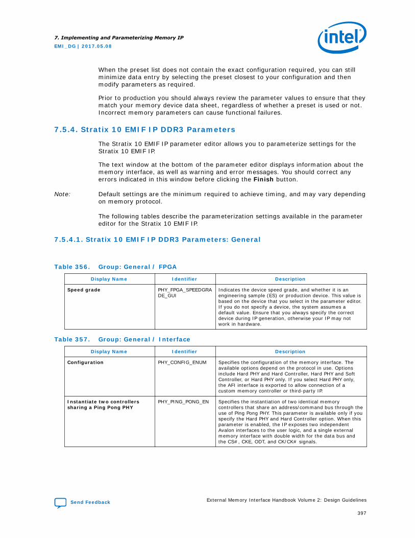
When the preset list does not contain the exact configuration required, you can stillminimize data entry by selecting the preset closest to your configuration and thenmodify parameters as required.
Prior to production you should always review the parameter values to ensure that theymatch your memory device data sheet, regardless of whether a preset is used or not.Incorrect memory parameters can cause functional failures.
7.5.4. Stratix 10 EMIF IP DDR3 Parameters
The Stratix 10 EMIF IP parameter editor allows you to parameterize settings for theStratix 10 EMIF IP.
The text window at the bottom of the parameter editor displays information about thememory interface, as well as warning and error messages. You should correct anyerrors indicated in this window before clicking the Finish button.
Note: Default settings are the minimum required to achieve timing, and may vary dependingon memory protocol.
The following tables describe the parameterization settings available in the parametereditor for the Stratix 10 EMIF IP.
7.5.4.1. Stratix 10 EMIF IP DDR3 Parameters: General
Table 356. Group: General / FPGA
Display Name Identifier Description
Speed grade PHY_FPGA_SPEEDGRADE_GUI
Indicates the device speed grade, and whether it is anengineering sample (ES) or production device. This value isbased on the device that you select in the parameter editor.If you do not specify a device, the system assumes adefault value. Ensure that you always specify the correctdevice during IP generation, otherwise your IP may notwork in hardware.
Table 357. Group: General / Interface
Display Name Identifier Description
Configuration PHY_CONFIG_ENUM Specifies the configuration of the memory interface. Theavailable options depend on the protocol in use. Optionsinclude Hard PHY and Hard Controller, Hard PHY and SoftController, or Hard PHY only. If you select Hard PHY only,the AFI interface is exported to allow connection of acustom memory controller or third-party IP.
Instantiate two controllerssharing a Ping Pong PHY
PHY_PING_PONG_EN Specifies the instantiation of two identical memorycontrollers that share an address/command bus through theuse of Ping Pong PHY. This parameter is available only if youspecify the Hard PHY and Hard Controller option. When thisparameter is enabled, the IP exposes two independentAvalon interfaces to the user logic, and a single externalmemory interface with double width for the data bus andthe CS#, CKE, ODT, and CK/CK# signals.
7. Implementing and Parameterizing Memory IP
EMI_DG | 2017.05.08
Send Feedback External Memory Interface Handbook Volume 2: Design Guidelines
397
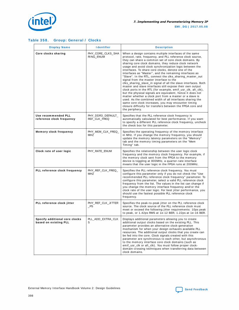
Table 358. Group: General / Clocks
Display Name Identifier Description
Core clocks sharing PHY_CORE_CLKS_SHARING_ENUM
When a design contains multiple interfaces of the sameprotocol, rate, frequency, and PLL reference clock source,they can share a common set of core clock domains. Bysharing core clock domains, they reduce clock networkusage and avoid clock synchronization logic between theinterfaces. To share core clocks, denote one of theinterfaces as "Master", and the remaining interfaces as"Slave". In the RTL, connect the clks_sharing_master_outsignal from the master interface to theclks_sharing_slave_in signal of all the slave interfaces. Bothmaster and slave interfaces still expose their own outputclock ports in the RTL (for example, emif_usr_clk, afi_clk),but the physical signals are equivalent, hence it does notmatter whether a clock port from a master or a slave isused. As the combined width of all interfaces sharing thesame core clock increases, you may encounter timingclosure difficulty for transfers between the FPGA core andthe periphery.
Use recommended PLLreference clock frequency
PHY_DDR3_DEFAULT_REF_CLK_FREQ
Specifies that the PLL reference clock frequency isautomatically calculated for best performance. If you wantto specify a different PLL reference clock frequency, uncheckthe check box for this parameter.
Memory clock frequency PHY_MEM_CLK_FREQ_MHZ
Specifies the operating frequency of the memory interfacein MHz. If you change the memory frequency, you shouldupdate the memory latency parameters on the "Memory"tab and the memory timing parameters on the "MemTiming" tab.
Clock rate of user logic PHY_RATE_ENUM Specifies the relationship between the user logic clockfrequency and the memory clock frequency. For example, ifthe memory clock sent from the FPGA to the memorydevice is toggling at 800MHz, a quarter-rate interfacemeans that the user logic in the FPGA runs at 200MHz.
PLL reference clock frequency PHY_REF_CLK_FREQ_MHZ
Specifies the PLL reference clock frequency. You mustconfigure this parameter only if you do not check the "Userecommended PLL reference clock frequency" parameter. Toconfigure this parameter, select a valid PLL reference clockfrequency from the list. The values in the list can change ifyou change the memory interface frequency and/or theclock rate of the user logic. For best jitter performance, youshould use the fastest possible PLL reference clockfrequency.
PLL reference clock jitter PHY_REF_CLK_JITTER_PS
Specifies the peak-to-peak jitter on the PLL reference clocksource. The clock source of the PLL reference clock mustmeet or exceed the following jitter requirements: 10ps peakto peak, or 1.42ps RMS at 1e-12 BER, 1.22ps at 1e-16 BER.
Specify additional core clocksbased on existing PLL
PLL_ADD_EXTRA_CLKS
Displays additional parameters allowing you to createadditional output clocks based on the existing PLL. Thisparameter provides an alternative clock-generationmechanism for when your design exhausts available PLLresources. The additional output clocks that you create canbe fed into the core. Clock signals created with thisparameter are synchronous to each other, but asynchronousto the memory interface core clock domains (such asemif_usr_clk or afi_clk). You must follow proper clock-domain-crossing techniques when transferring data betweenclock domains.
7. Implementing and Parameterizing Memory IP
EMI_DG | 2017.05.08
External Memory Interface Handbook Volume 2: Design Guidelines Send Feedback
398
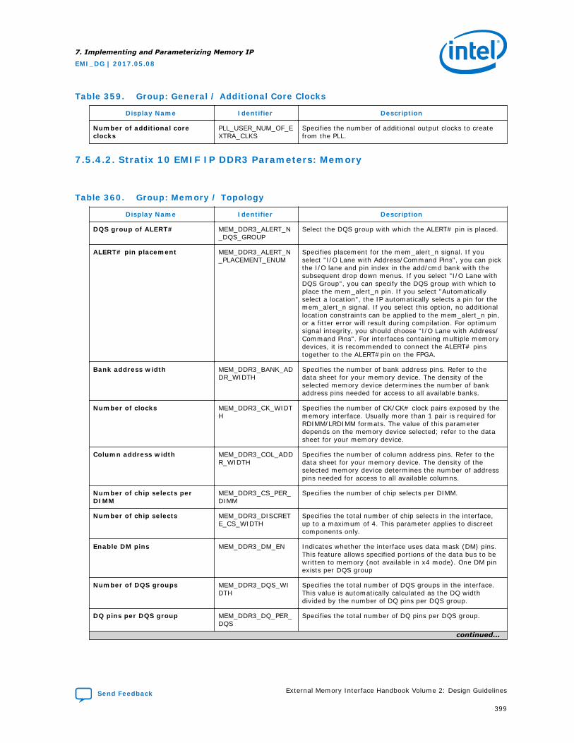
Table 359. Group: General / Additional Core Clocks
Display Name Identifier Description
Number of additional coreclocks
PLL_USER_NUM_OF_EXTRA_CLKS
Specifies the number of additional output clocks to createfrom the PLL.
7.5.4.2. Stratix 10 EMIF IP DDR3 Parameters: Memory
Table 360. Group: Memory / Topology
Display Name Identifier Description
DQS group of ALERT# MEM_DDR3_ALERT_N_DQS_GROUP
Select the DQS group with which the ALERT# pin is placed.
ALERT# pin placement MEM_DDR3_ALERT_N_PLACEMENT_ENUM
Specifies placement for the mem_alert_n signal. If youselect "I/O Lane with Address/Command Pins", you can pickthe I/O lane and pin index in the add/cmd bank with thesubsequent drop down menus. If you select "I/O Lane withDQS Group", you can specify the DQS group with which toplace the mem_alert_n pin. If you select "Automaticallyselect a location", the IP automatically selects a pin for themem_alert_n signal. If you select this option, no additionallocation constraints can be applied to the mem_alert_n pin,or a fitter error will result during compilation. For optimumsignal integrity, you should choose "I/O Lane with Address/Command Pins". For interfaces containing multiple memorydevices, it is recommended to connect the ALERT# pinstogether to the ALERT#pin on the FPGA.
Bank address width MEM_DDR3_BANK_ADDR_WIDTH
Specifies the number of bank address pins. Refer to thedata sheet for your memory device. The density of theselected memory device determines the number of bankaddress pins needed for access to all available banks.
Number of clocks MEM_DDR3_CK_WIDTH
Specifies the number of CK/CK# clock pairs exposed by thememory interface. Usually more than 1 pair is required forRDIMM/LRDIMM formats. The value of this parameterdepends on the memory device selected; refer to the datasheet for your memory device.
Column address width MEM_DDR3_COL_ADDR_WIDTH
Specifies the number of column address pins. Refer to thedata sheet for your memory device. The density of theselected memory device determines the number of addresspins needed for access to all available columns.
Number of chip selects perDIMM
MEM_DDR3_CS_PER_DIMM
Specifies the number of chip selects per DIMM.
Number of chip selects MEM_DDR3_DISCRETE_CS_WIDTH
Specifies the total number of chip selects in the interface,up to a maximum of 4. This parameter applies to discreetcomponents only.
Enable DM pins MEM_DDR3_DM_EN Indicates whether the interface uses data mask (DM) pins.This feature allows specified portions of the data bus to bewritten to memory (not available in x4 mode). One DM pinexists per DQS group
Number of DQS groups MEM_DDR3_DQS_WIDTH
Specifies the total number of DQS groups in the interface.This value is automatically calculated as the DQ widthdivided by the number of DQ pins per DQS group.
DQ pins per DQS group MEM_DDR3_DQ_PER_DQS
Specifies the total number of DQ pins per DQS group.
continued...
7. Implementing and Parameterizing Memory IP
EMI_DG | 2017.05.08
Send Feedback External Memory Interface Handbook Volume 2: Design Guidelines
399
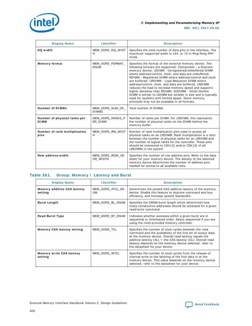
Display Name Identifier Description
DQ width MEM_DDR3_DQ_WIDTH
Specifies the total number of data pins in the interface. Themaximum supported width is 144, or 72 in Ping Pong PHYmode.
Memory format MEM_DDR3_FORMAT_ENUM
Specifies the format of the external memory device. Thefollowing formats are supported: Component - a Discretememory device; UDIMM - Unregistered/Unbuffered DIMMwhere address/control, clock, and data are unbuffered;RDIMM - Registered DIMM where address/control and clockare buffered; LRDIMM - Load Reduction DIMM whereaddress/control, clock, and data are buffered. LRDIMMreduces the load to increase memory speed and supportshigher densities than RDIMM; SODIMM - Small OutlineDIMM is similar to UDIMM but smaller in size and is typicallyused for systems with limited space. Some memoryprotocols may not be available in all formats.
Number of DIMMs MEM_DDR3_NUM_OF_DIMMS
Total number of DIMMs.
Number of physical ranks perDIMM
MEM_DDR3_RANKS_PER_DIMM
Number of ranks per DIMM. For LRDIMM, this representsthe number of physical ranks on the DIMM behind thememory buffer
Number of rank multiplicationpins
MEM_DDR3_RM_WIDTH
Number of rank multiplication pins used to access allphysical ranks on an LRDIMM. Rank multiplication is a ratiobetween the number of physical ranks for an LRDIMM andthe number of logical ranks for the controller. These pinsshould be connected to CS#[2] and/or CS#[3] of allLRDIMMs in the system
Row address width MEM_DDR3_ROW_ADDR_WIDTH
Specifies the number of row address pins. Refer to the datasheet for your memory device. The density of the selectedmemory device determines the number of address pinsneeded for access to all available rows.
Table 361. Group: Memory / Latency and Burst
Display Name Identifier Description
Memory additive CAS latencysetting
MEM_DDR3_ATCL_ENUM
Determines the posted CAS additive latency of the memorydevice. Enable this feature to improve command and busefficiency, and increase system bandwidth.
Burst Length MEM_DDR3_BL_ENUM Specifies the DRAM burst length which determines howmany consecutive addresses should be accessed for a givenread/write command.
Read Burst Type MEM_DDR3_BT_ENUM Indicates whether accesses within a given burst are insequential or interleaved order. Select sequential if you areusing the Intel-provided memory controller.
Memory CAS latency setting MEM_DDR3_TCL Specifies the number of clock cycles between the readcommand and the availability of the first bit of output dataat the memory device. Overall read latency equals theadditive latency (AL) + the CAS latency (CL). Overall readlatency depends on the memory device selected; refer tothe datasheet for your device.
Memory write CAS latencysetting
MEM_DDR3_WTCL Specifies the number of clock cycles from the release ofinternal write to the latching of the first data in at thememory device. This value depends on the memory deviceselected; refer to the datasheet for your device.
7. Implementing and Parameterizing Memory IP
EMI_DG | 2017.05.08
External Memory Interface Handbook Volume 2: Design Guidelines Send Feedback
400
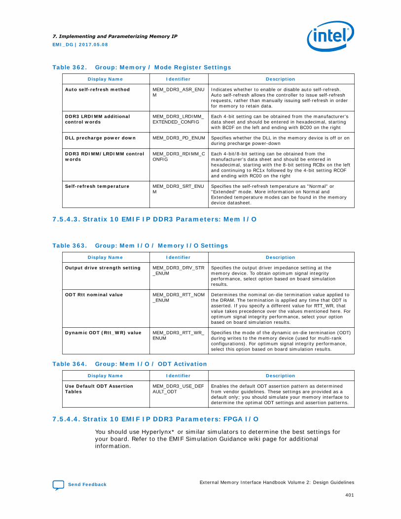
Table 362. Group: Memory / Mode Register Settings
Display Name Identifier Description
Auto self-refresh method MEM_DDR3_ASR_ENUM
Indicates whether to enable or disable auto self-refresh.Auto self-refresh allows the controller to issue self-refreshrequests, rather than manually issuing self-refresh in orderfor memory to retain data.
DDR3 LRDIMM additionalcontrol words
MEM_DDR3_LRDIMM_EXTENDED_CONFIG
Each 4-bit setting can be obtained from the manufacturer'sdata sheet and should be entered in hexadecimal, startingwith BC0F on the left and ending with BC00 on the right
DLL precharge power down MEM_DDR3_PD_ENUM Specifies whether the DLL in the memory device is off or onduring precharge power-down
DDR3 RDIMM/LRDIMM controlwords
MEM_DDR3_RDIMM_CONFIG
Each 4-bit/8-bit setting can be obtained from themanufacturer's data sheet and should be entered inhexadecimal, starting with the 8-bit setting RCBx on the leftand continuing to RC1x followed by the 4-bit setting RCOFand ending with RC00 on the right
Self-refresh temperature MEM_DDR3_SRT_ENUM
Specifies the self-refresh temperature as "Normal" or"Extended" mode. More information on Normal andExtended temperature modes can be found in the memorydevice datasheet.
7.5.4.3. Stratix 10 EMIF IP DDR3 Parameters: Mem I/O
Table 363. Group: Mem I/O / Memory I/O Settings
Display Name Identifier Description
Output drive strength setting MEM_DDR3_DRV_STR_ENUM
Specifies the output driver impedance setting at thememory device. To obtain optimum signal integrityperformance, select option based on board simulationresults.
ODT Rtt nominal value MEM_DDR3_RTT_NOM_ENUM
Determines the nominal on-die termination value applied tothe DRAM. The termination is applied any time that ODT isasserted. If you specify a different value for RTT_WR, thatvalue takes precedence over the values mentioned here. Foroptimum signal integrity performance, select your optionbased on board simulation results.
Dynamic ODT (Rtt_WR) value MEM_DDR3_RTT_WR_ENUM
Specifies the mode of the dynamic on-die termination (ODT)during writes to the memory device (used for multi-rankconfigurations). For optimum signal integrity performance,select this option based on board simulation results.
Table 364. Group: Mem I/O / ODT Activation
Display Name Identifier Description
Use Default ODT AssertionTables
MEM_DDR3_USE_DEFAULT_ODT
Enables the default ODT assertion pattern as determinedfrom vendor guidelines. These settings are provided as adefault only; you should simulate your memory interface todetermine the optimal ODT settings and assertion patterns.
7.5.4.4. Stratix 10 EMIF IP DDR3 Parameters: FPGA I/O
You should use Hyperlynx* or similar simulators to determine the best settings foryour board. Refer to the EMIF Simulation Guidance wiki page for additionalinformation.
7. Implementing and Parameterizing Memory IP
EMI_DG | 2017.05.08
Send Feedback External Memory Interface Handbook Volume 2: Design Guidelines
401
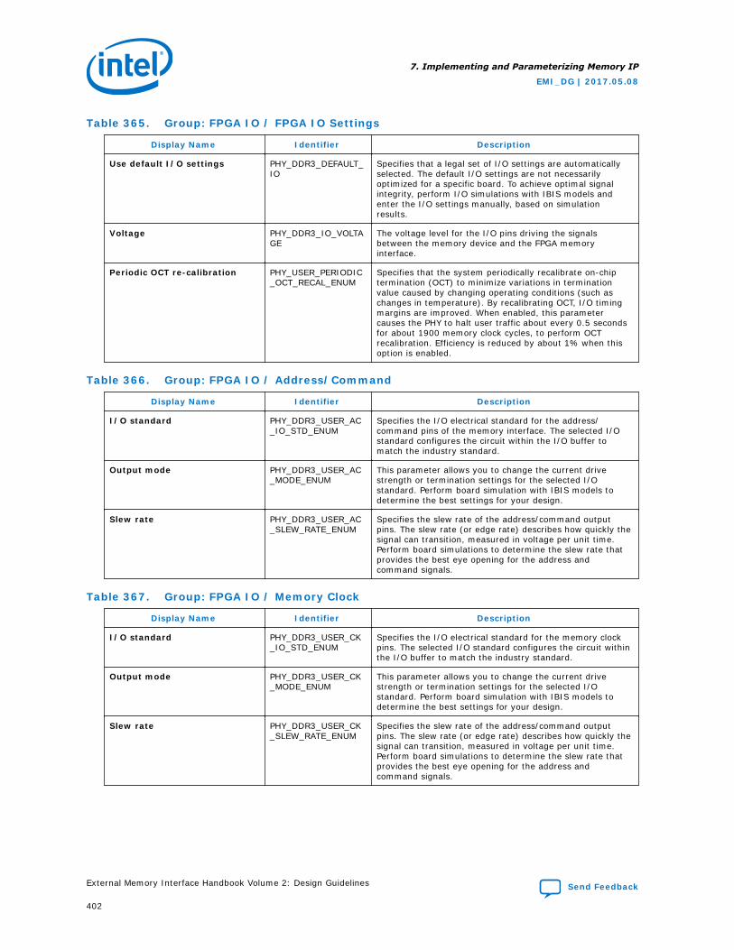
Table 365. Group: FPGA IO / FPGA IO Settings
Display Name Identifier Description
Use default I/O settings PHY_DDR3_DEFAULT_IO
Specifies that a legal set of I/O settings are automaticallyselected. The default I/O settings are not necessarilyoptimized for a specific board. To achieve optimal signalintegrity, perform I/O simulations with IBIS models andenter the I/O settings manually, based on simulationresults.
Voltage PHY_DDR3_IO_VOLTAGE
The voltage level for the I/O pins driving the signalsbetween the memory device and the FPGA memoryinterface.
Periodic OCT re-calibration PHY_USER_PERIODIC_OCT_RECAL_ENUM
Specifies that the system periodically recalibrate on-chiptermination (OCT) to minimize variations in terminationvalue caused by changing operating conditions (such aschanges in temperature). By recalibrating OCT, I/O timingmargins are improved. When enabled, this parametercauses the PHY to halt user traffic about every 0.5 secondsfor about 1900 memory clock cycles, to perform OCTrecalibration. Efficiency is reduced by about 1% when thisoption is enabled.
Table 366. Group: FPGA IO / Address/Command
Display Name Identifier Description
I/O standard PHY_DDR3_USER_AC_IO_STD_ENUM
Specifies the I/O electrical standard for the address/command pins of the memory interface. The selected I/Ostandard configures the circuit within the I/O buffer tomatch the industry standard.
Output mode PHY_DDR3_USER_AC_MODE_ENUM
This parameter allows you to change the current drivestrength or termination settings for the selected I/Ostandard. Perform board simulation with IBIS models todetermine the best settings for your design.
Slew rate PHY_DDR3_USER_AC_SLEW_RATE_ENUM
Specifies the slew rate of the address/command outputpins. The slew rate (or edge rate) describes how quickly thesignal can transition, measured in voltage per unit time.Perform board simulations to determine the slew rate thatprovides the best eye opening for the address andcommand signals.
Table 367. Group: FPGA IO / Memory Clock
Display Name Identifier Description
I/O standard PHY_DDR3_USER_CK_IO_STD_ENUM
Specifies the I/O electrical standard for the memory clockpins. The selected I/O standard configures the circuit withinthe I/O buffer to match the industry standard.
Output mode PHY_DDR3_USER_CK_MODE_ENUM
This parameter allows you to change the current drivestrength or termination settings for the selected I/Ostandard. Perform board simulation with IBIS models todetermine the best settings for your design.
Slew rate PHY_DDR3_USER_CK_SLEW_RATE_ENUM
Specifies the slew rate of the address/command outputpins. The slew rate (or edge rate) describes how quickly thesignal can transition, measured in voltage per unit time.Perform board simulations to determine the slew rate thatprovides the best eye opening for the address andcommand signals.
7. Implementing and Parameterizing Memory IP
EMI_DG | 2017.05.08
External Memory Interface Handbook Volume 2: Design Guidelines Send Feedback
402
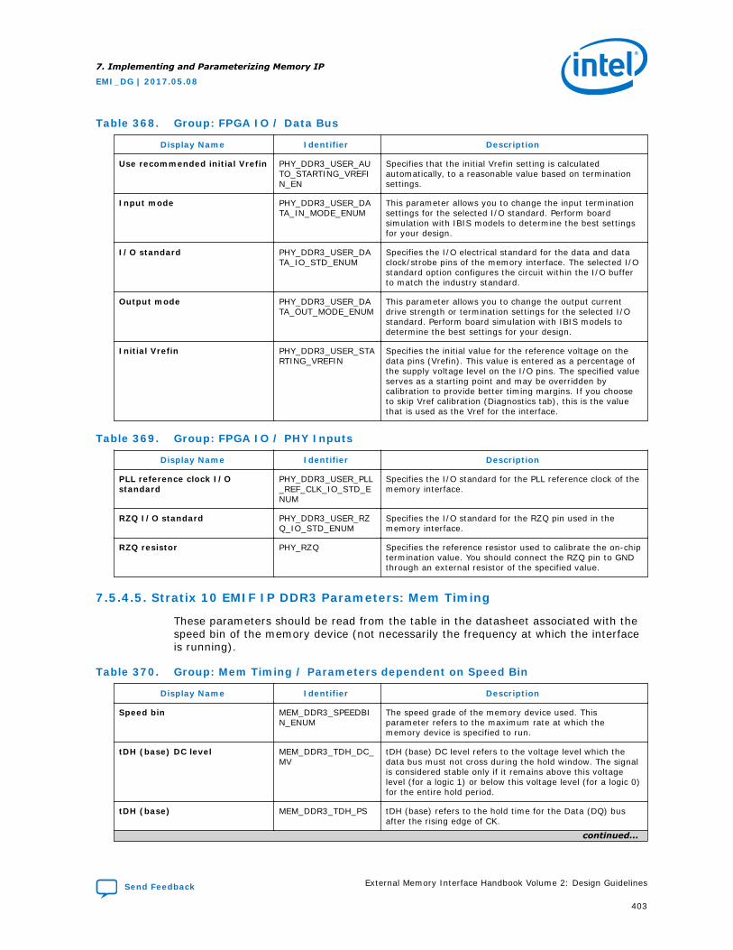
Table 368. Group: FPGA IO / Data Bus
Display Name Identifier Description
Use recommended initial Vrefin PHY_DDR3_USER_AUTO_STARTING_VREFIN_EN
Specifies that the initial Vrefin setting is calculatedautomatically, to a reasonable value based on terminationsettings.
Input mode PHY_DDR3_USER_DATA_IN_MODE_ENUM
This parameter allows you to change the input terminationsettings for the selected I/O standard. Perform boardsimulation with IBIS models to determine the best settingsfor your design.
I/O standard PHY_DDR3_USER_DATA_IO_STD_ENUM
Specifies the I/O electrical standard for the data and dataclock/strobe pins of the memory interface. The selected I/Ostandard option configures the circuit within the I/O bufferto match the industry standard.
Output mode PHY_DDR3_USER_DATA_OUT_MODE_ENUM
This parameter allows you to change the output currentdrive strength or termination settings for the selected I/Ostandard. Perform board simulation with IBIS models todetermine the best settings for your design.
Initial Vrefin PHY_DDR3_USER_STARTING_VREFIN
Specifies the initial value for the reference voltage on thedata pins (Vrefin). This value is entered as a percentage ofthe supply voltage level on the I/O pins. The specified valueserves as a starting point and may be overridden bycalibration to provide better timing margins. If you chooseto skip Vref calibration (Diagnostics tab), this is the valuethat is used as the Vref for the interface.
Table 369. Group: FPGA IO / PHY Inputs
Display Name Identifier Description
PLL reference clock I/Ostandard
PHY_DDR3_USER_PLL_REF_CLK_IO_STD_ENUM
Specifies the I/O standard for the PLL reference clock of thememory interface.
RZQ I/O standard PHY_DDR3_USER_RZQ_IO_STD_ENUM
Specifies the I/O standard for the RZQ pin used in thememory interface.
RZQ resistor PHY_RZQ Specifies the reference resistor used to calibrate the on-chiptermination value. You should connect the RZQ pin to GNDthrough an external resistor of the specified value.
7.5.4.5. Stratix 10 EMIF IP DDR3 Parameters: Mem Timing
These parameters should be read from the table in the datasheet associated with thespeed bin of the memory device (not necessarily the frequency at which the interfaceis running).
Table 370. Group: Mem Timing / Parameters dependent on Speed Bin
Display Name Identifier Description
Speed bin MEM_DDR3_SPEEDBIN_ENUM
The speed grade of the memory device used. Thisparameter refers to the maximum rate at which thememory device is specified to run.
tDH (base) DC level MEM_DDR3_TDH_DC_MV
tDH (base) DC level refers to the voltage level which thedata bus must not cross during the hold window. The signalis considered stable only if it remains above this voltagelevel (for a logic 1) or below this voltage level (for a logic 0)for the entire hold period.
tDH (base) MEM_DDR3_TDH_PS tDH (base) refers to the hold time for the Data (DQ) busafter the rising edge of CK.
continued...
7. Implementing and Parameterizing Memory IP
EMI_DG | 2017.05.08
Send Feedback External Memory Interface Handbook Volume 2: Design Guidelines
403

Display Name Identifier Description
tDQSCK MEM_DDR3_TDQSCK_PS
tDQSCK describes the skew between the memory clock (CK)and the input data strobes (DQS) used for reads. It is thetime between the rising data strobe edge (DQS, DQS#)relative to the rising CK edge.
tDQSQ MEM_DDR3_TDQSQ_PS
tDQSQ describes the latest valid transition of the associatedDQ pins for a READ. tDQSQ specifically refers to the DQS,DQS# to DQ skew. It is the length of time between theDQS, DQS# crossing to the last valid transition of theslowest DQ pin in the DQ group associated with that DQSstrobe.
tDQSS MEM_DDR3_TDQSS_CYC
tDQSS describes the skew between the memory clock (CK)and the output data strobes used for writes. It is the timebetween the rising data strobe edge (DQS, DQS#) relativeto the rising CK edge.
tDSH MEM_DDR3_TDSH_CYC
tDSH specifies the write DQS hold time. This is the timedifference between the rising CK edge and the falling edgeof DQS, measured as a percentage of tCK.
tDSS MEM_DDR3_TDSS_CYC
tDSS describes the time between the falling edge of DQS tothe rising edge of the next CK transition.
tDS (base) AC level MEM_DDR3_TDS_AC_MV
tDS (base) AC level refers to the voltage level which thedata bus must cross and remain above during the setupmargin window. The signal is considered stable only if itremains above this voltage level (for a logic 1) or below thisvoltage level (for a logic 0) for the entire setup period.
tDS (base) MEM_DDR3_TDS_PS tDS(base) refers to the setup time for the Data (DQ) busbefore the rising edge of the DQS strobe.
tIH (base) DC level MEM_DDR3_TIH_DC_MV
tIH (base) DC level refers to the voltage level which theaddress/command signal must not cross during the holdwindow. The signal is considered stable only if it remainsabove this voltage level (for a logic 1) or below this voltagelevel (for a logic 0) for the entire hold period.
tIH (base) MEM_DDR3_TIH_PS tIH (base) refers to the hold time for the Address/Command(A) bus after the rising edge of CK. Depending on what AClevel the user has chosen for a design, the hold margin canvary (this variance will be automatically determined whenthe user choses the "tIH (base) AC level").
tINIT MEM_DDR3_TINIT_US tINIT describes the time duration of the memoryinitialization after a device power-up. After RESET_n is de-asserted, wait for another 500us until CKE becomes active.During this time, the DRAM starts internal initialization; thishappens independently of external clocks.
tIS (base) AC level MEM_DDR3_TIS_AC_MV
tIS (base) AC level refers to the voltage level which theaddress/command signal must cross and remain aboveduring the setup margin window. The signal is consideredstable only if it remains above this voltage level (for a logic1) or below this voltage level (for a logic 0) for the entiresetup period.
tIS (base) MEM_DDR3_TIS_PS tIS (base) refers to the setup time for the Address/Command/Control (A) bus to the rising edge of CK.
tMRD MEM_DDR3_TMRD_CK_CYC
The mode register set command cycle time, tMRD is theminimum time period required between two MRScommands.
continued...
7. Implementing and Parameterizing Memory IP
EMI_DG | 2017.05.08
External Memory Interface Handbook Volume 2: Design Guidelines Send Feedback
404
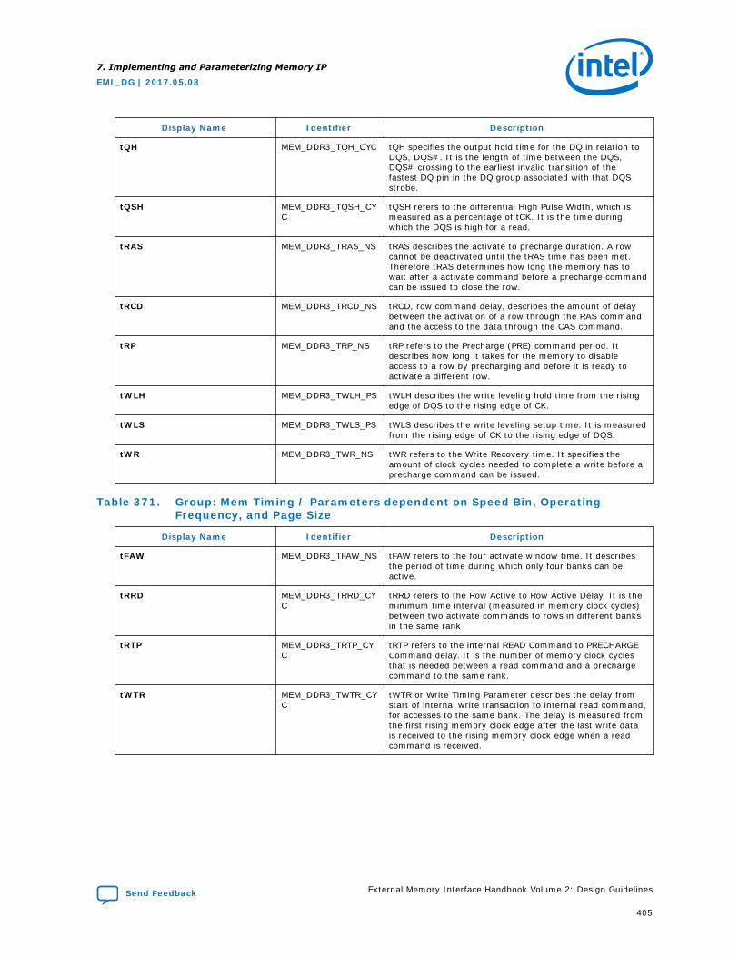
Display Name Identifier Description
tQH MEM_DDR3_TQH_CYC tQH specifies the output hold time for the DQ in relation toDQS, DQS#. It is the length of time between the DQS,DQS# crossing to the earliest invalid transition of thefastest DQ pin in the DQ group associated with that DQSstrobe.
tQSH MEM_DDR3_TQSH_CYC
tQSH refers to the differential High Pulse Width, which ismeasured as a percentage of tCK. It is the time duringwhich the DQS is high for a read.
tRAS MEM_DDR3_TRAS_NS tRAS describes the activate to precharge duration. A rowcannot be deactivated until the tRAS time has been met.Therefore tRAS determines how long the memory has towait after a activate command before a precharge commandcan be issued to close the row.
tRCD MEM_DDR3_TRCD_NS tRCD, row command delay, describes the amount of delaybetween the activation of a row through the RAS commandand the access to the data through the CAS command.
tRP MEM_DDR3_TRP_NS tRP refers to the Precharge (PRE) command period. Itdescribes how long it takes for the memory to disableaccess to a row by precharging and before it is ready toactivate a different row.
tWLH MEM_DDR3_TWLH_PS tWLH describes the write leveling hold time from the risingedge of DQS to the rising edge of CK.
tWLS MEM_DDR3_TWLS_PS tWLS describes the write leveling setup time. It is measuredfrom the rising edge of CK to the rising edge of DQS.
tWR MEM_DDR3_TWR_NS tWR refers to the Write Recovery time. It specifies theamount of clock cycles needed to complete a write before aprecharge command can be issued.
Table 371. Group: Mem Timing / Parameters dependent on Speed Bin, OperatingFrequency, and Page Size
Display Name Identifier Description
tFAW MEM_DDR3_TFAW_NS tFAW refers to the four activate window time. It describesthe period of time during which only four banks can beactive.
tRRD MEM_DDR3_TRRD_CYC
tRRD refers to the Row Active to Row Active Delay. It is theminimum time interval (measured in memory clock cycles)between two activate commands to rows in different banksin the same rank
tRTP MEM_DDR3_TRTP_CYC
tRTP refers to the internal READ Command to PRECHARGECommand delay. It is the number of memory clock cyclesthat is needed between a read command and a prechargecommand to the same rank.
tWTR MEM_DDR3_TWTR_CYC
tWTR or Write Timing Parameter describes the delay fromstart of internal write transaction to internal read command,for accesses to the same bank. The delay is measured fromthe first rising memory clock edge after the last write datais received to the rising memory clock edge when a readcommand is received.
7. Implementing and Parameterizing Memory IP
EMI_DG | 2017.05.08
Send Feedback External Memory Interface Handbook Volume 2: Design Guidelines
405

Table 372. Group: Mem Timing / Parameters dependent on Density and Temperature
Display Name Identifier Description
tREFI MEM_DDR3_TREFI_US tREFI refers to the average periodic refresh interval. It isthe maximum amount of time the memory can tolerate inbetween each refresh command
tRFC MEM_DDR3_TRFC_NS tRFC refers to the Refresh Cycle Time. It is the amount ofdelay after a refresh command before an activate commandcan be accepted by the memory. This parameter isdependent on the memory density and is necessary forproper hardware functionality.
7.5.4.6. Stratix 10 EMIF IP DDR3 Parameters: Board
Table 373. Group: Board / Intersymbol Interference/Crosstalk
Display Name Identifier Description
Address and command ISI/crosstalk
BOARD_DDR3_USER_AC_ISI_NS
The address and command window reduction due to ISI andcrosstalk effects. The number to be entered is the total lossof margin on both the setup and hold sides (measured losson the setup side + measured loss on the hold side). Referto the EMIF Simulation Guidance wiki page for additionalinformation.
Read DQS/DQS# ISI/crosstalk BOARD_DDR3_USER_RCLK_ISI_NS
The reduction of the read data window due to ISI andcrosstalk effects on the DQS/DQS# signal when driven bythe memory device during a read. The number to beentered is the total loss of margin on the setup and holdsides (measured loss on the setup side + measured loss onthe hold side). Refer to the EMIF Simulation Guidance wikipage for additional information.
Read DQ ISI/crosstalk BOARD_DDR3_USER_RDATA_ISI_NS
The reduction of the read data window due to ISI andcrosstalk effects on the DQ signal when driven by thememory device during a read. The number to be entered isthe total loss of margin on the setup and hold side(measured loss on the setup side + measured loss on thehold side). Refer to the EMIF Simulation Guidance wiki pagefor additional information.
Write DQS/DQS# ISI/crosstalk BOARD_DDR3_USER_WCLK_ISI_NS
The reduction of the write data window due to ISI andcrosstalk effects on the DQS/DQS# signal when driven bythe FPGA during a write. The number to be entered is thetotal loss of margin on the setup and hold sides (measuredloss on the setup side + measured loss on the hold side).Refer to the EMIF Simulation Guidance wiki page foradditional information.
Write DQ ISI/crosstalk BOARD_DDR3_USER_WDATA_ISI_NS
The reduction of the write data window due to ISI andcrosstalk effects on the DQ signal when driven by the FPGAduring a write. The number to be entered is the total loss ofmargin on the setup and hold sides (measured loss on thesetup side + measured loss on the hold side). Refer to theEMIF Simulation Guidance wiki page for additionalinformation.
Use default ISI/crosstalkvalues
BOARD_DDR3_USE_DEFAULT_ISI_VALUES
You can enable this option to use default intersymbolinterference and crosstalk values for your topology. Notethat the default values are not optimized for your board. Foroptimal signal integrity, it is recommended that you do notenable this parameter, but instead perform I/O simulationusing IBIS models and Hyperlynx*, and manually entervalues based on your simulation results, instead of usingthe default values.
7. Implementing and Parameterizing Memory IP
EMI_DG | 2017.05.08
External Memory Interface Handbook Volume 2: Design Guidelines Send Feedback
406

Table 374. Group: Board / Board and Package Skews
Display Name Identifier Description
Average delay differencebetween address/commandand CK
BOARD_DDR3_AC_TO_CK_SKEW_NS
The average delay difference between the address/command signals and the CK signal, calculated by averagingthe longest and smallest address/command signal tracedelay minus the maximum CK trace delay. Positive valuesrepresent address and command signals that are longerthan CK signals and negative values represent address andcommand signals that are shorter than CK signals.
Maximum board skew withinDQS group
BOARD_DDR3_BRD_SKEW_WITHIN_DQS_NS
The largest skew between all DQ and DM pins in a DQSgroup. This value affects the read capture and writemargins.
Average delay differencebetween DQS and CK
BOARD_DDR3_DQS_TO_CK_SKEW_NS
The average delay difference between the DQS signals andthe CK signal, calculated by averaging the longest andsmallest DQS trace delay minus the CK trace delay. Positivevalues represent DQS signals that are longer than CKsignals and negative values represent DQS signals that areshorter than CK signals.
Package deskewed with boardlayout (address/commandbus)
BOARD_DDR3_IS_SKEW_WITHIN_AC_DESKEWED
Enable this parameter if you are compensating for packageskew on the address, command, control, and memory clockbuses in the board layout. Include package skew incalculating the following board skew parameters.
Package deskewed with boardlayout (DQS group)
BOARD_DDR3_IS_SKEW_WITHIN_DQS_DESKEWED
Enable this parameter if you are compensating for packageskew on the DQ, DQS, and DM buses in the board layout.Include package skew in calculating the following boardskew parameters.
Maximum CK delay to DIMM/device
BOARD_DDR3_MAX_CK_DELAY_NS
The delay of the longest CK trace from the FPGA to anyDIMM/device.
Maximum DQS delay to DIMM/device
BOARD_DDR3_MAX_DQS_DELAY_NS
The delay of the longest DQS trace from the FPGA to anyDIMM/device
Maximum system skew withinaddress/command bus
BOARD_DDR3_PKG_BRD_SKEW_WITHIN_AC_NS
Maximum system skew within address/command bus refersto the largest skew between the address and commandsignals.
Maximum delay differencebetween DIMMs/devices
BOARD_DDR3_SKEW_BETWEEN_DIMMS_NS
The largest propagation delay on DQ signals between ranks(applicable only when there is more than one rank). Forexample: when you configure two ranks using one DIMMthere is a short distance between the ranks for the same DQpin; when you implement two ranks using two DIMMs thedistance is larger.
Maximum skew between DQSgroups
BOARD_DDR3_SKEW_BETWEEN_DQS_NS
The largest skew between DQS signals.
7.5.4.7. Stratix 10 EMIF IP DDR3 Parameters: Controller
7. Implementing and Parameterizing Memory IP
EMI_DG | 2017.05.08
Send Feedback External Memory Interface Handbook Volume 2: Design Guidelines
407
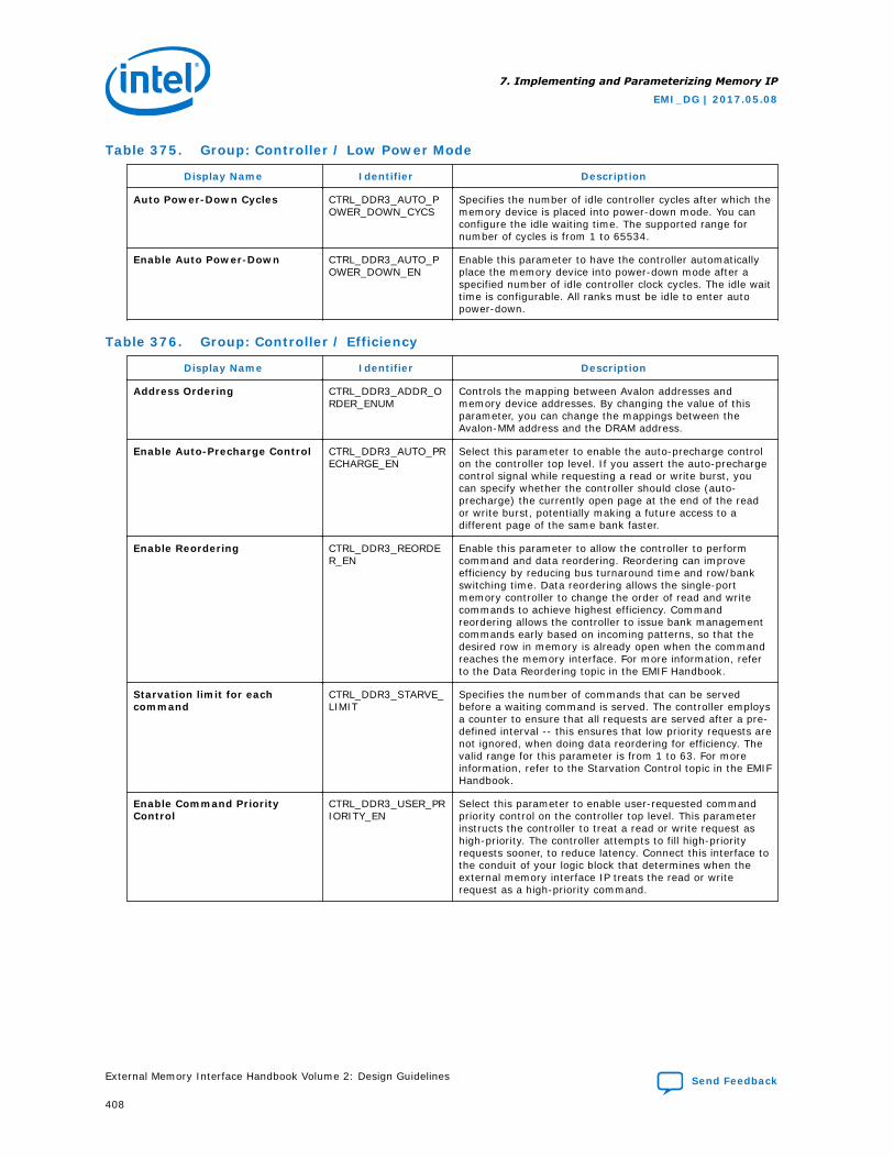
Table 375. Group: Controller / Low Power Mode
Display Name Identifier Description
Auto Power-Down Cycles CTRL_DDR3_AUTO_POWER_DOWN_CYCS
Specifies the number of idle controller cycles after which thememory device is placed into power-down mode. You canconfigure the idle waiting time. The supported range fornumber of cycles is from 1 to 65534.
Enable Auto Power-Down CTRL_DDR3_AUTO_POWER_DOWN_EN
Enable this parameter to have the controller automaticallyplace the memory device into power-down mode after aspecified number of idle controller clock cycles. The idle waittime is configurable. All ranks must be idle to enter autopower-down.
Table 376. Group: Controller / Efficiency
Display Name Identifier Description
Address Ordering CTRL_DDR3_ADDR_ORDER_ENUM
Controls the mapping between Avalon addresses andmemory device addresses. By changing the value of thisparameter, you can change the mappings between theAvalon-MM address and the DRAM address.
Enable Auto-Precharge Control CTRL_DDR3_AUTO_PRECHARGE_EN
Select this parameter to enable the auto-precharge controlon the controller top level. If you assert the auto-prechargecontrol signal while requesting a read or write burst, youcan specify whether the controller should close (auto-precharge) the currently open page at the end of the reador write burst, potentially making a future access to adifferent page of the same bank faster.
Enable Reordering CTRL_DDR3_REORDER_EN
Enable this parameter to allow the controller to performcommand and data reordering. Reordering can improveefficiency by reducing bus turnaround time and row/bankswitching time. Data reordering allows the single-portmemory controller to change the order of read and writecommands to achieve highest efficiency. Commandreordering allows the controller to issue bank managementcommands early based on incoming patterns, so that thedesired row in memory is already open when the commandreaches the memory interface. For more information, referto the Data Reordering topic in the EMIF Handbook.
Starvation limit for eachcommand
CTRL_DDR3_STARVE_LIMIT
Specifies the number of commands that can be servedbefore a waiting command is served. The controller employsa counter to ensure that all requests are served after a pre-defined interval -- this ensures that low priority requests arenot ignored, when doing data reordering for efficiency. Thevalid range for this parameter is from 1 to 63. For moreinformation, refer to the Starvation Control topic in the EMIFHandbook.
Enable Command PriorityControl
CTRL_DDR3_USER_PRIORITY_EN
Select this parameter to enable user-requested commandpriority control on the controller top level. This parameterinstructs the controller to treat a read or write request ashigh-priority. The controller attempts to fill high-priorityrequests sooner, to reduce latency. Connect this interface tothe conduit of your logic block that determines when theexternal memory interface IP treats the read or writerequest as a high-priority command.
7. Implementing and Parameterizing Memory IP
EMI_DG | 2017.05.08
External Memory Interface Handbook Volume 2: Design Guidelines Send Feedback
408
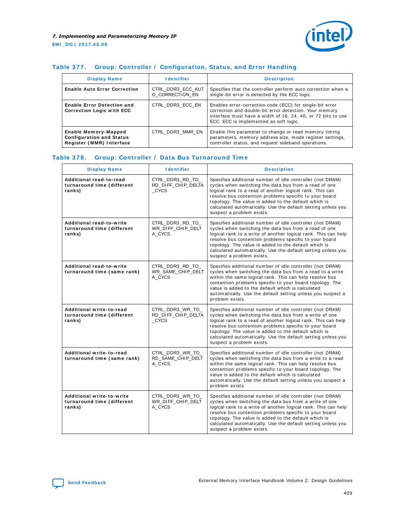
Table 377. Group: Controller / Configuration, Status, and Error Handling
Display Name Identifier Description
Enable Auto Error Correction CTRL_DDR3_ECC_AUTO_CORRECTION_EN
Specifies that the controller perform auto correction when asingle-bit error is detected by the ECC logic.
Enable Error Detection andCorrection Logic with ECC
CTRL_DDR3_ECC_EN Enables error-correction code (ECC) for single-bit errorcorrection and double-bit error detection. Your memoryinterface must have a width of 16, 24, 40, or 72 bits to useECC. ECC is implemented as soft logic.
Enable Memory-MappedConfiguration and StatusRegister (MMR) Interface
CTRL_DDR3_MMR_EN Enable this parameter to change or read memory timingparameters, memory address size, mode register settings,controller status, and request sideband operations.
Table 378. Group: Controller / Data Bus Turnaround Time
Display Name Identifier Description
Additional read-to-readturnaround time (differentranks)
CTRL_DDR3_RD_TO_RD_DIFF_CHIP_DELTA_CYCS
Specifies additional number of idle controller (not DRAM)cycles when switching the data bus from a read of onelogical rank to a read of another logical rank. This canresolve bus contention problems specific to your boardtopology. The value is added to the default which iscalculated automatically. Use the default setting unless yoususpect a problem exists.
Additional read-to-writeturnaround time (differentranks)
CTRL_DDR3_RD_TO_WR_DIFF_CHIP_DELTA_CYCS
Specifies additional number of idle controller (not DRAM)cycles when switching the data bus from a read of onelogical rank to a write of another logical rank. This can helpresolve bus contention problems specific to your boardtopology. The value is added to the default which iscalculated automatically. Use the default setting unless yoususpect a problem exists.
Additional read-to-writeturnaround time (same rank)
CTRL_DDR3_RD_TO_WR_SAME_CHIP_DELTA_CYCS
Specifies additional number of idle controller (not DRAM)cycles when switching the data bus from a read to a writewithin the same logical rank. This can help resolve buscontention problems specific to your board topology. Thevalue is added to the default which is calculatedautomatically. Use the default setting unless you suspect aproblem exists.
Additional write-to-readturnaround time (differentranks)
CTRL_DDR3_WR_TO_RD_DIFF_CHIP_DELTA_CYCS
Specifies additional number of idle controller (not DRAM)cycles when switching the data bus from a write of onelogical rank to a read of another logical rank. This can helpresolve bus contention problems specific to your boardtopology. The value is added to the default which iscalculated automatically. Use the default setting unless yoususpect a problem exists.
Additional write-to-readturnaround time (same rank)
CTRL_DDR3_WR_TO_RD_SAME_CHIP_DELTA_CYCS
Specifies additional number of idle controller (not DRAM)cycles when switching the data bus from a write to a readwithin the same logical rank. This can help resolve buscontention problems specific to your board topology. Thevalue is added to the default which is calculatedautomatically. Use the default setting unless you suspect aproblem exists.
Additional write-to-writeturnaround time (differentranks)
CTRL_DDR3_WR_TO_WR_DIFF_CHIP_DELTA_CYCS
Specifies additional number of idle controller (not DRAM)cycles when switching the data bus from a write of onelogical rank to a write of another logical rank. This can helpresolve bus contention problems specific to your boardtopology. The value is added to the default which iscalculated automatically. Use the default setting unless yoususpect a problem exists.
7. Implementing and Parameterizing Memory IP
EMI_DG | 2017.05.08
Send Feedback External Memory Interface Handbook Volume 2: Design Guidelines
409

7.5.4.8. Stratix 10 EMIF IP DDR3 Parameters: Diagnostics
Table 379. Group: Diagnostics / Simulation Options
Display Name Identifier Description
Abstract phy for fast simulation DIAG_DDR3_ABSTRACT_PHY
Specifies that the system use Abstract PHY for simulation.Abstract PHY replaces the PHY with a model for fastsimulation and can reduce simulation time by 2-3 times.Abstract PHY is available for certain protocols and devicefamilies, and only when you select Skip Calibration.
Calibration mode DIAG_SIM_CAL_MODE_ENUM
Specifies whether to skip memory interface calibrationduring simulation, or to simulate the full calibration process.Simulating the full calibration process can take hours (oreven days), depending on the width and depth of thememory interface. You can achieve much faster simulationtimes by skipping the calibration process, but that is onlyexpected to work when the memory model is ideal and theinterconnect delays are zero. If you enable this parameter,the interface still performs some memory initializationbefore starting normal operations. Abstract PHY issupported with skip calibration.
Table 380. Group: Diagnostics / Calibration Debug Options
Display Name Identifier Description
Enable Daisy-Chaining forQuartus Prime EMIF DebugToolkit/On-Chip Debug Port
DIAG_EXPORT_SEQ_AVALON_MASTER
Specifies that the IP export an Avalon-MM master interface(cal_debug_out) which can connect to the cal_debuginterface of other EMIF cores residing in the same I/Ocolumn. This parameter applies only if the EMIF DebugToolkit or On-Chip Debug Port is enabled. Refer to theDebugging Multiple EMIFs wiki page for more informationabout debugging multiple EMIFs.
Quartus Prime EMIF DebugToolkit/On-Chip Debug Port
DIAG_EXPORT_SEQ_AVALON_SLAVE
Specifies the connectivity of an Avalon slave interface foruse by the Quartus Prime EMIF Debug Toolkit or user corelogic. If you set this parameter to "Disabled," no debugfeatures are enabled. If you set this parameter to "Export,"an Avalon slave interface named "cal_debug" is exportedfrom the IP. To use this interface with the EMIF DebugToolkit, you must instantiate and connect an EMIF debuginterface IP core to it, or connect it to the cal_debug_outinterface of another EMIF core. If you select "Add EMIFDebug Interface", an EMIF debug interface componentcontaining a JTAG Avalon Master is connected to the debugport, allowing the core to be accessed by the EMIF DebugToolkit. Only one EMIF debug interface should beinstantiated per I/O column. You can chain additional EMIFor PHYLite cores to the first by enabling the "Enable Daisy-Chaining for Quartus Prime EMIF Debug Toolkit/On-ChipDebug Port" option for all cores in the chain, and selecting"Export" for the "Quartus Prime EMIF Debug Toolkit/On-ChipDebug Port" option on all cores after the first.
Interface ID DIAG_INTERFACE_ID Identifies interfaces within the I/O column, for use by theEMIF Debug Toolkit and the On-Chip Debug Port. InterfaceIDs should be unique among EMIF cores within the sameI/O column. If the Quartus Prime EMIF Debug Toolkit/On-Chip Debug Port parameter is set to Disabled, the interfaceID is unused.
Use Soft NIOS Processor forOn-Chip Debug
DIAG_SOFT_NIOS_MODE
Enables a soft Nios processor as a peripheral component toaccess the On-Chip Debug Port. Only one interface in acolumn can activate this option.
7. Implementing and Parameterizing Memory IP
EMI_DG | 2017.05.08
External Memory Interface Handbook Volume 2: Design Guidelines Send Feedback
410
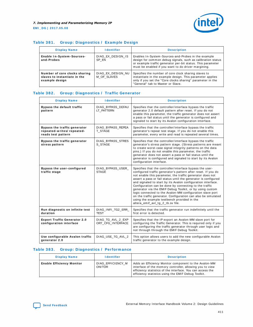
Table 381. Group: Diagnostics / Example Design
Display Name Identifier Description
Enable In-System-Sources-and-Probes
DIAG_EX_DESIGN_ISSP_EN
Enables In-System-Sources-and-Probes in the exampledesign for common debug signals, such as calibration statusor example traffic generator per-bit status. This parametermust be enabled if you want to do driver margining.
Number of core clocks sharingslaves to instantiate in theexample design
DIAG_EX_DESIGN_NUM_OF_SLAVES
Specifies the number of core clock sharing slaves toinstantiate in the example design. This parameter appliesonly if you set the "Core clocks sharing" parameter in the"General" tab to Master or Slave.
Table 382. Group: Diagnostics / Traffic Generator
Display Name Identifier Description
Bypass the default trafficpattern
DIAG_BYPASS_DEFAULT_PATTERN
Specifies that the controller/interface bypass the trafficgenerator 2.0 default pattern after reset. If you do notenable this parameter, the traffic generator does not asserta pass or fail status until the generator is configured andsignaled to start by its Avalon configuration interface.
Bypass the traffic generatorrepeated-writes/repeated-reads test pattern
DIAG_BYPASS_REPEAT_STAGE
Specifies that the controller/interface bypass the trafficgenerator's repeat test stage. If you do not enable thisparameter, every write and read is repeated several times.
Bypass the traffic generatorstress pattern
DIAG_BYPASS_STRESS_STAGE
Specifies that the controller/interface bypass the trafficgenerator's stress pattern stage. (Stress patterns are meantto create worst-case signal integrity patterns on the datapins.) If you do not enable this parameter, the trafficgenerator does not assert a pass or fail status until thegenerator is configured and signaled to start by its Avalonconfiguration interface.
Bypass the user-configuredtraffic stage
DIAG_BYPASS_USER_STAGE
Specifies that the controller/interface bypass the user-configured traffic generator's pattern after reset. If you donot enable this parameter, the traffic generator does notassert a pass or fail status until the generator is configuredand signaled to start by its Avalon configuration interface.Configuration can be done by connecting to the trafficgenerator via the EMIF Debug Toolkit, or by using customlogic connected to the Avalon-MM configuration slave porton the traffic generator. Configuration can also be simulatedusing the example testbench provided in thealtera_emif_avl_tg_2_tb.sv file.
Run diagnostic on infinite testduration
DIAG_INFI_TG2_ERR_TEST
Specifies that the traffic generator run indefinitely until thefirst error is detected.
Export Traffic Generator 2.0configuration interface
DIAG_TG_AVL_2_EXPORT_CFG_INTERFACE
Specifies that the IP export an Avalon-MM slave port forconfiguring the Traffic Generator. This is required only if youare configuring the traffic generator through user logic andnot through through the EMIF Debug Toolkit.
Use configurable Avalon trafficgenerator 2.0
DIAG_USE_TG_AVL_2 This option allows users to add the new configurable Avalontraffic generator to the example design.
Table 383. Group: Diagnostics / Performance
Display Name Identifier Description
Enable Efficiency Monitor DIAG_EFFICIENCY_MONITOR
Adds an Efficiency Monitor component to the Avalon-MMinterface of the memory controller, allowing you to viewefficiency statistics of the interface. You can access theefficiency statistics using the EMIF Debug Toolkit.
7. Implementing and Parameterizing Memory IP
EMI_DG | 2017.05.08
Send Feedback External Memory Interface Handbook Volume 2: Design Guidelines
411

Table 384. Group: Diagnostics / Miscellaneous
Display Name Identifier Description
Use short Qsys interface names SHORT_QSYS_INTERFACE_NAMES
Specifies the use of short interface names, for improvedusability and consistency with other Qsys components. Ifthis parameter is disabled, the names of Qsys interfacesexposed by the IP will include the type and direction of theinterface. Long interface names are supported forbackward-compatibility and will be removed in a futurerelease.
7.5.4.9. Stratix 10 EMIF IP DDR3 Parameters: Example Designs
Table 385. Group: Example Designs / Available Example Designs
Display Name Identifier Description
Select design EX_DESIGN_GUI_DDR3_SEL_DESIGN
Specifies the creation of a full Quartus Prime project,instantiating an external memory interface and an exampletraffic generator, according to your parameterization. Afterthe design is created, you can specify the target device andpin location assignments, run a full compilation, verifytiming closure, and test the interface on your board usingthe programming file created by the Quartus Primeassembler. The 'Generate Example Design' button lets yougenerate simulation or synthesis file sets.
Table 386. Group: Example Designs / Example Design Files
Display Name Identifier Description
Simulation EX_DESIGN_GUI_DDR3_GEN_SIM
Specifies that the 'Generate Example Design' button createall necessary file sets for simulation. Expect a shortadditional delay as the file set is created. If you do notenable this parameter, simulation file sets are not created.Instead, the output directory will contain the ed_sim.qsysfile which holds Qsys details of the simulation exampledesign, and a make_sim_design.tcl file with othercorresponding tcl files. You can run make_sim_design.tclfrom a command line to generate the simulation exampledesign. The generated example designs for varioussimulators are stored in the /sim sub-directory.
Synthesis EX_DESIGN_GUI_DDR3_GEN_SYNTH
Specifies that the 'Generate Example Design' button createall necessary file sets for synthesis. Expect a shortadditional delay as the file set is created. If you do notenable this parameter, synthesis file sets are not created.Instead, the output directory will contain the ed_synth.qsysfile which holds Qsys details of the synthesis exampledesign, and a make_qii_design.tcl script with othercorresponding tcl files. You can run make_qii_design.tclfrom a command line to generate the synthesis exampledesign. The generated example design is stored in the /qiisub-directory.
Table 387. Group: Example Designs / Generated HDL Format
Display Name Identifier Description
Simulation HDL format EX_DESIGN_GUI_DDR3_HDL_FORMAT
This option lets you choose the format of HDL in whichgenerated simulation files are created.
7. Implementing and Parameterizing Memory IP
EMI_DG | 2017.05.08
External Memory Interface Handbook Volume 2: Design Guidelines Send Feedback
412
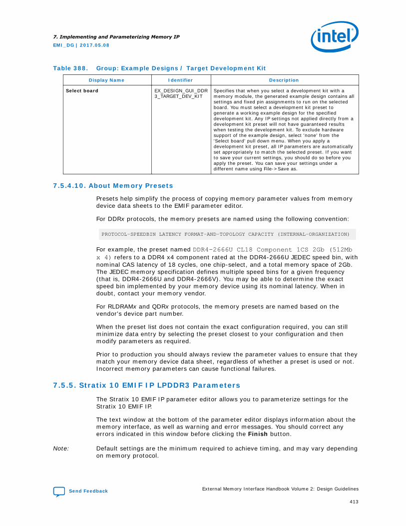
Table 388. Group: Example Designs / Target Development Kit
Display Name Identifier Description
Select board EX_DESIGN_GUI_DDR3_TARGET_DEV_KIT
Specifies that when you select a development kit with amemory module, the generated example design contains allsettings and fixed pin assignments to run on the selectedboard. You must select a development kit preset togenerate a working example design for the specifieddevelopment kit. Any IP settings not applied directly from adevelopment kit preset will not have guaranteed resultswhen testing the development kit. To exclude hardwaresupport of the example design, select 'none' from the'Select board' pull down menu. When you apply adevelopment kit preset, all IP parameters are automaticallyset appropriately to match the selected preset. If you wantto save your current settings, you should do so before youapply the preset. You can save your settings under adifferent name using File->Save as.
7.5.4.10. About Memory Presets
Presets help simplify the process of copying memory parameter values from memorydevice data sheets to the EMIF parameter editor.
For DDRx protocols, the memory presets are named using the following convention:
PROTOCOL-SPEEDBIN LATENCY FORMAT-AND-TOPOLOGY CAPACITY (INTERNAL-ORGANIZATION)
For example, the preset named DDR4-2666U CL18 Component 1CS 2Gb (512Mbx 4) refers to a DDR4 x4 component rated at the DDR4-2666U JEDEC speed bin, withnominal CAS latency of 18 cycles, one chip-select, and a total memory space of 2Gb.The JEDEC memory specification defines multiple speed bins for a given frequency(that is, DDR4-2666U and DDR4-2666V). You may be able to determine the exactspeed bin implemented by your memory device using its nominal latency. When indoubt, contact your memory vendor.
For RLDRAMx and QDRx protocols, the memory presets are named based on thevendor's device part number.
When the preset list does not contain the exact configuration required, you can stillminimize data entry by selecting the preset closest to your configuration and thenmodify parameters as required.
Prior to production you should always review the parameter values to ensure that theymatch your memory device data sheet, regardless of whether a preset is used or not.Incorrect memory parameters can cause functional failures.
7.5.5. Stratix 10 EMIF IP LPDDR3 Parameters
The Stratix 10 EMIF IP parameter editor allows you to parameterize settings for theStratix 10 EMIF IP.
The text window at the bottom of the parameter editor displays information about thememory interface, as well as warning and error messages. You should correct anyerrors indicated in this window before clicking the Finish button.
Note: Default settings are the minimum required to achieve timing, and may vary dependingon memory protocol.
7. Implementing and Parameterizing Memory IP
EMI_DG | 2017.05.08
Send Feedback External Memory Interface Handbook Volume 2: Design Guidelines
413
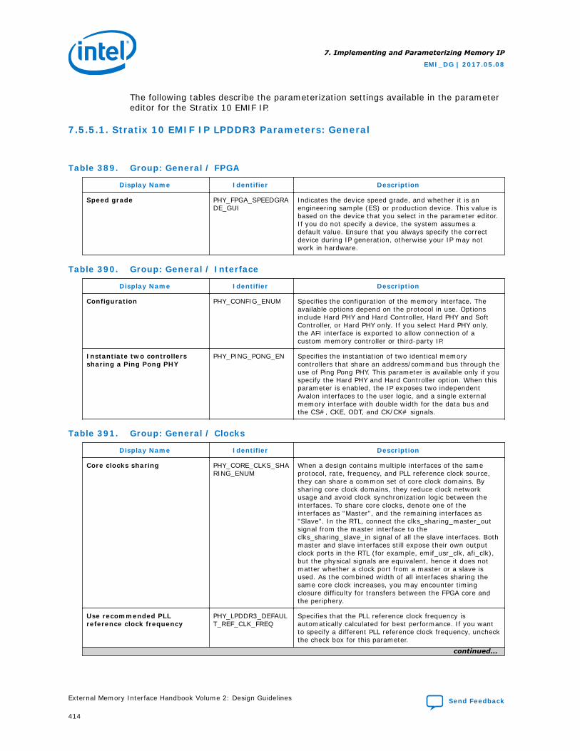
The following tables describe the parameterization settings available in the parametereditor for the Stratix 10 EMIF IP.
7.5.5.1. Stratix 10 EMIF IP LPDDR3 Parameters: General
Table 389. Group: General / FPGA
Display Name Identifier Description
Speed grade PHY_FPGA_SPEEDGRADE_GUI
Indicates the device speed grade, and whether it is anengineering sample (ES) or production device. This value isbased on the device that you select in the parameter editor.If you do not specify a device, the system assumes adefault value. Ensure that you always specify the correctdevice during IP generation, otherwise your IP may notwork in hardware.
Table 390. Group: General / Interface
Display Name Identifier Description
Configuration PHY_CONFIG_ENUM Specifies the configuration of the memory interface. Theavailable options depend on the protocol in use. Optionsinclude Hard PHY and Hard Controller, Hard PHY and SoftController, or Hard PHY only. If you select Hard PHY only,the AFI interface is exported to allow connection of acustom memory controller or third-party IP.
Instantiate two controllerssharing a Ping Pong PHY
PHY_PING_PONG_EN Specifies the instantiation of two identical memorycontrollers that share an address/command bus through theuse of Ping Pong PHY. This parameter is available only if youspecify the Hard PHY and Hard Controller option. When thisparameter is enabled, the IP exposes two independentAvalon interfaces to the user logic, and a single externalmemory interface with double width for the data bus andthe CS#, CKE, ODT, and CK/CK# signals.
Table 391. Group: General / Clocks
Display Name Identifier Description
Core clocks sharing PHY_CORE_CLKS_SHARING_ENUM
When a design contains multiple interfaces of the sameprotocol, rate, frequency, and PLL reference clock source,they can share a common set of core clock domains. Bysharing core clock domains, they reduce clock networkusage and avoid clock synchronization logic between theinterfaces. To share core clocks, denote one of theinterfaces as "Master", and the remaining interfaces as"Slave". In the RTL, connect the clks_sharing_master_outsignal from the master interface to theclks_sharing_slave_in signal of all the slave interfaces. Bothmaster and slave interfaces still expose their own outputclock ports in the RTL (for example, emif_usr_clk, afi_clk),but the physical signals are equivalent, hence it does notmatter whether a clock port from a master or a slave isused. As the combined width of all interfaces sharing thesame core clock increases, you may encounter timingclosure difficulty for transfers between the FPGA core andthe periphery.
Use recommended PLLreference clock frequency
PHY_LPDDR3_DEFAULT_REF_CLK_FREQ
Specifies that the PLL reference clock frequency isautomatically calculated for best performance. If you wantto specify a different PLL reference clock frequency, uncheckthe check box for this parameter.
continued...
7. Implementing and Parameterizing Memory IP
EMI_DG | 2017.05.08
External Memory Interface Handbook Volume 2: Design Guidelines Send Feedback
414
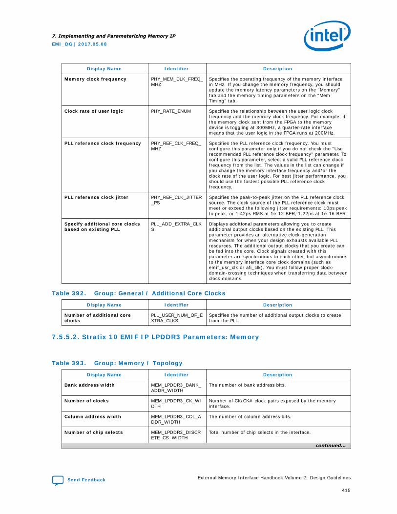
Display Name Identifier Description
Memory clock frequency PHY_MEM_CLK_FREQ_MHZ
Specifies the operating frequency of the memory interfacein MHz. If you change the memory frequency, you shouldupdate the memory latency parameters on the "Memory"tab and the memory timing parameters on the "MemTiming" tab.
Clock rate of user logic PHY_RATE_ENUM Specifies the relationship between the user logic clockfrequency and the memory clock frequency. For example, ifthe memory clock sent from the FPGA to the memorydevice is toggling at 800MHz, a quarter-rate interfacemeans that the user logic in the FPGA runs at 200MHz.
PLL reference clock frequency PHY_REF_CLK_FREQ_MHZ
Specifies the PLL reference clock frequency. You mustconfigure this parameter only if you do not check the "Userecommended PLL reference clock frequency" parameter. Toconfigure this parameter, select a valid PLL reference clockfrequency from the list. The values in the list can change ifyou change the memory interface frequency and/or theclock rate of the user logic. For best jitter performance, youshould use the fastest possible PLL reference clockfrequency.
PLL reference clock jitter PHY_REF_CLK_JITTER_PS
Specifies the peak-to-peak jitter on the PLL reference clocksource. The clock source of the PLL reference clock mustmeet or exceed the following jitter requirements: 10ps peakto peak, or 1.42ps RMS at 1e-12 BER, 1.22ps at 1e-16 BER.
Specify additional core clocksbased on existing PLL
PLL_ADD_EXTRA_CLKS
Displays additional parameters allowing you to createadditional output clocks based on the existing PLL. Thisparameter provides an alternative clock-generationmechanism for when your design exhausts available PLLresources. The additional output clocks that you create canbe fed into the core. Clock signals created with thisparameter are synchronous to each other, but asynchronousto the memory interface core clock domains (such asemif_usr_clk or afi_clk). You must follow proper clock-domain-crossing techniques when transferring data betweenclock domains.
Table 392. Group: General / Additional Core Clocks
Display Name Identifier Description
Number of additional coreclocks
PLL_USER_NUM_OF_EXTRA_CLKS
Specifies the number of additional output clocks to createfrom the PLL.
7.5.5.2. Stratix 10 EMIF IP LPDDR3 Parameters: Memory
Table 393. Group: Memory / Topology
Display Name Identifier Description
Bank address width MEM_LPDDR3_BANK_ADDR_WIDTH
The number of bank address bits.
Number of clocks MEM_LPDDR3_CK_WIDTH
Number of CK/CK# clock pairs exposed by the memoryinterface.
Column address width MEM_LPDDR3_COL_ADDR_WIDTH
The number of column address bits.
Number of chip selects MEM_LPDDR3_DISCRETE_CS_WIDTH
Total number of chip selects in the interface.
continued...
7. Implementing and Parameterizing Memory IP
EMI_DG | 2017.05.08
Send Feedback External Memory Interface Handbook Volume 2: Design Guidelines
415
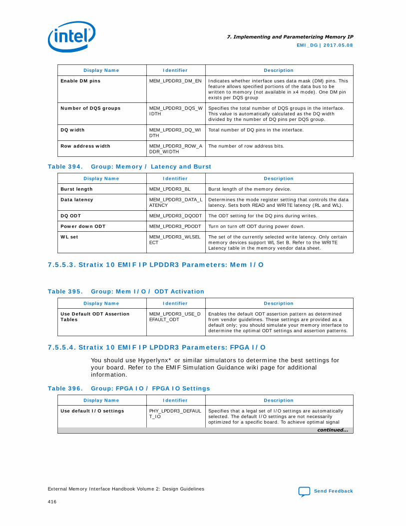
Display Name Identifier Description
Enable DM pins MEM_LPDDR3_DM_EN Indicates whether interface uses data mask (DM) pins. Thisfeature allows specified portions of the data bus to bewritten to memory (not available in x4 mode). One DM pinexists per DQS group
Number of DQS groups MEM_LPDDR3_DQS_WIDTH
Specifies the total number of DQS groups in the interface.This value is automatically calculated as the DQ widthdivided by the number of DQ pins per DQS group.
DQ width MEM_LPDDR3_DQ_WIDTH
Total number of DQ pins in the interface.
Row address width MEM_LPDDR3_ROW_ADDR_WIDTH
The number of row address bits.
Table 394. Group: Memory / Latency and Burst
Display Name Identifier Description
Burst length MEM_LPDDR3_BL Burst length of the memory device.
Data latency MEM_LPDDR3_DATA_LATENCY
Determines the mode register setting that controls the datalatency. Sets both READ and WRITE latency (RL and WL).
DQ ODT MEM_LPDDR3_DQODT The ODT setting for the DQ pins during writes.
Power down ODT MEM_LPDDR3_PDODT Turn on turn off ODT during power down.
WL set MEM_LPDDR3_WLSELECT
The set of the currently selected write latency. Only certainmemory devices support WL Set B. Refer to the WRITELatency table in the memory vendor data sheet.
7.5.5.3. Stratix 10 EMIF IP LPDDR3 Parameters: Mem I/O
Table 395. Group: Mem I/O / ODT Activation
Display Name Identifier Description
Use Default ODT AssertionTables
MEM_LPDDR3_USE_DEFAULT_ODT
Enables the default ODT assertion pattern as determinedfrom vendor guidelines. These settings are provided as adefault only; you should simulate your memory interface todetermine the optimal ODT settings and assertion patterns.
7.5.5.4. Stratix 10 EMIF IP LPDDR3 Parameters: FPGA I/O
You should use Hyperlynx* or similar simulators to determine the best settings foryour board. Refer to the EMIF Simulation Guidance wiki page for additionalinformation.
Table 396. Group: FPGA IO / FPGA IO Settings
Display Name Identifier Description
Use default I/O settings PHY_LPDDR3_DEFAULT_IO
Specifies that a legal set of I/O settings are automaticallyselected. The default I/O settings are not necessarilyoptimized for a specific board. To achieve optimal signal
continued...
7. Implementing and Parameterizing Memory IP
EMI_DG | 2017.05.08
External Memory Interface Handbook Volume 2: Design Guidelines Send Feedback
416
Display Name Identifier Description
integrity, perform I/O simulations with IBIS models andenter the I/O settings manually, based on simulationresults.
Voltage PHY_LPDDR3_IO_VOLTAGE
The voltage level for the I/O pins driving the signalsbetween the memory device and the FPGA memoryinterface.
Periodic OCT re-calibration PHY_USER_PERIODIC_OCT_RECAL_ENUM
Specifies that the system periodically recalibrate on-chiptermination (OCT) to minimize variations in terminationvalue caused by changing operating conditions (such aschanges in temperature). By recalibrating OCT, I/O timingmargins are improved. When enabled, this parametercauses the PHY to halt user traffic about every 0.5 secondsfor about 1900 memory clock cycles, to perform OCTrecalibration. Efficiency is reduced by about 1% when thisoption is enabled.
Table 397. Group: FPGA IO / Address/Command
Display Name Identifier Description
I/O standard PHY_LPDDR3_USER_AC_IO_STD_ENUM
Specifies the I/O electrical standard for the address/command pins of the memory interface. The selected I/Ostandard configures the circuit within the I/O buffer tomatch the industry standard.
Output mode PHY_LPDDR3_USER_AC_MODE_ENUM
This parameter allows you to change the current drivestrength or termination settings for the selected I/Ostandard. Perform board simulation with IBIS models todetermine the best settings for your design.
Slew rate PHY_LPDDR3_USER_AC_SLEW_RATE_ENUM
Specifies the slew rate of the address/command outputpins. The slew rate (or edge rate) describes how quickly thesignal can transition, measured in voltage per unit time.Perform board simulations to determine the slew rate thatprovides the best eye opening for the address andcommand signals.
Table 398. Group: FPGA IO / Memory Clock
Display Name Identifier Description
I/O standard PHY_LPDDR3_USER_CK_IO_STD_ENUM
Specifies the I/O electrical standard for the memory clockpins. The selected I/O standard configures the circuit withinthe I/O buffer to match the industry standard.
Output mode PHY_LPDDR3_USER_CK_MODE_ENUM
This parameter allows you to change the current drivestrength or termination settings for the selected I/Ostandard. Perform board simulation with IBIS models todetermine the best settings for your design.
Slew rate PHY_LPDDR3_USER_CK_SLEW_RATE_ENUM
Specifies the slew rate of the address/command outputpins. The slew rate (or edge rate) describes how quickly thesignal can transition, measured in voltage per unit time.Perform board simulations to determine the slew rate thatprovides the best eye opening for the address andcommand signals.
7. Implementing and Parameterizing Memory IP
EMI_DG | 2017.05.08
Send Feedback External Memory Interface Handbook Volume 2: Design Guidelines
417

Table 399. Group: FPGA IO / Data Bus
Display Name Identifier Description
Use recommended initial Vrefin PHY_LPDDR3_USER_AUTO_STARTING_VREFIN_EN
Specifies that the initial Vrefin setting is calculatedautomatically, to a reasonable value based on terminationsettings.
Input mode PHY_LPDDR3_USER_DATA_IN_MODE_ENUM
This parameter allows you to change the input terminationsettings for the selected I/O standard. Perform boardsimulation with IBIS models to determine the best settingsfor your design.
I/O standard PHY_LPDDR3_USER_DATA_IO_STD_ENUM
Specifies the I/O electrical standard for the data and dataclock/strobe pins of the memory interface. The selected I/Ostandard option configures the circuit within the I/O bufferto match the industry standard.
Output mode PHY_LPDDR3_USER_DATA_OUT_MODE_ENUM
This parameter allows you to change the output currentdrive strength or termination settings for the selected I/Ostandard. Perform board simulation with IBIS models todetermine the best settings for your design.
Initial Vrefin PHY_LPDDR3_USER_STARTING_VREFIN
Specifies the initial value for the reference voltage on thedata pins (Vrefin). This value is entered as a percentage ofthe supply voltage level on the I/O pins. The specified valueserves as a starting point and may be overridden bycalibration to provide better timing margins. If you chooseto skip Vref calibration (Diagnostics tab), this is the valuethat is used as the Vref for the interface.
Table 400. Group: FPGA IO / PHY Inputs
Display Name Identifier Description
PLL reference clock I/Ostandard
PHY_LPDDR3_USER_PLL_REF_CLK_IO_STD_ENUM
Specifies the I/O standard for the PLL reference clock of thememory interface.
RZQ I/O standard PHY_LPDDR3_USER_RZQ_IO_STD_ENUM
Specifies the I/O standard for the RZQ pin used in thememory interface.
RZQ resistor PHY_RZQ Specifies the reference resistor used to calibrate the on-chiptermination value. You should connect the RZQ pin to GNDthrough an external resistor of the specified value.
7.5.5.5. Stratix 10 EMIF IP LPDDR3 Parameters: Mem Timing
These parameters should be read from the table in the datasheet associated with thespeed bin of the memory device (not necessarily the frequency at which the interfaceis running).
Table 401. Group: Mem Timing / Parameters dependent on Speed Bin
Display Name Identifier Description
Speed bin MEM_LPDDR3_SPEEDBIN_ENUM
The speed grade of the memory device used. Thisparameter refers to the maximum rate at which thememory device is specified to run.
tDH (base) DC level MEM_LPDDR3_TDH_DC_MV
tDH (base) DC level refers to the voltage level which thedata bus must not cross during the hold window. The signalis considered stable only if it remains above this voltagelevel (for a logic 1) or below this voltage level (for a logic 0)for the entire hold period.
tDH (base) MEM_LPDDR3_TDH_PS
tDH (base) refers to the hold time for the Data (DQ) busafter the rising edge of CK.
continued...
7. Implementing and Parameterizing Memory IP
EMI_DG | 2017.05.08
External Memory Interface Handbook Volume 2: Design Guidelines Send Feedback
418

Display Name Identifier Description
tDQSCK MEM_LPDDR3_TDQSCK_PS
tDQSCK describes the skew between the memory clock (CK)and the input data strobes (DQS) used for reads. It is thetime between the rising data strobe edge (DQS, DQS#)relative to the rising CK edge.
tDQSQ MEM_LPDDR3_TDQSQ_PS
tDQSQ describes the latest valid transition of the associatedDQ pins for a READ. tDQSQ specifically refers to the DQS,DQS# to DQ skew. It is the length of time between theDQS, DQS# crossing to the last valid transition of theslowest DQ pin in the DQ group associated with that DQSstrobe.
tDSH MEM_LPDDR3_TDSH_CYC
tDSH specifies the write DQS hold time. This is the timedifference between the rising CK edge and the falling edgeof DQS, measured as a percentage of tCK.
tDSS MEM_LPDDR3_TDSS_CYC
tDSS describes the time between the falling edge of DQS tothe rising edge of the next CK transition.
tDS (base) AC level MEM_LPDDR3_TDS_AC_MV
tDS (base) AC level refers to the voltage level which thedata bus must cross and remain above during the setupmargin window. The signal is considered stable only if itremains above this voltage level (for a logic 1) or below thisvoltage level (for a logic 0) for the entire setup period.
tDS (base) MEM_LPDDR3_TDS_PS
tDS(base) refers to the setup time for the Data (DQ) busbefore the rising edge of the DQS strobe.
tIHCA (base) DC level MEM_LPDDR3_TIH_DC_MV
DC level of tIH (base) for derating purpose
tIHCA (base) MEM_LPDDR3_TIH_PS Address and control hold after CK clock rise
tINIT MEM_LPDDR3_TINIT_US
tINIT describes the time duration of the memoryinitialization after a device power-up. After RESET_n is de-asserted, wait for another 500us until CKE becomes active.During this time, the DRAM will start internal initialization;this will be done independently of external clocks.
tISCA (base) AC level MEM_LPDDR3_TIS_AC_MV
AC level of tIS (base) for derating purpose
tISCA (base) MEM_LPDDR3_TIS_PS Address and control setup to CK clock rise
tMRR MEM_LPDDR3_TMRR_CK_CYC
tMRR describes the minimum MODE REGISTER READcommand period.
tMRW MEM_LPDDR3_TMRW_CK_CYC
tMRW describes the minimum MODE REGISTER WRITEcommand period.
tQH MEM_LPDDR3_TQH_CYC
tQH specifies the output hold time for the DQ in relation toDQS, DQS#. It is the length of time between the DQS,DQS# crossing to the earliest invalid transition of thefastest DQ pin in the DQ group associated with that DQSstrobe.
tQSH MEM_LPDDR3_TQSH_CYC
tQSH refers to the differential High Pulse Width, which ismeasured as a percentage of tCK. It is the time duringwhich the DQS is high for a read.
tRAS MEM_LPDDR3_TRAS_NS
tRAS describes the activate to precharge duration. A rowcannot be deactivated until the tRAS time has been met.Therefore tRAS determines how long the memory has towait after a activate command before a precharge commandcan be issued to close the row.
tRCD MEM_LPDDR3_TRCD_NS
tRCD, row command delay, describes the amount of delaybetween the activation of a row through the RAS commandand the access to the data through the CAS command.
continued...
7. Implementing and Parameterizing Memory IP
EMI_DG | 2017.05.08
Send Feedback External Memory Interface Handbook Volume 2: Design Guidelines
419

Display Name Identifier Description
tWLH MEM_LPDDR3_TWLH_PS
tWLH describes the write leveling hold time from the risingedge of DQS to the rising edge of CK.
tWLS MEM_LPDDR3_TWLS_PS
tWLS describes the write leveling setup time. It is measuredfrom the rising edge of CK to the rising edge of DQS.
tWR MEM_LPDDR3_TWR_NS
tWR refers to the Write Recovery time. It specifies theamount of clock cycles needed to complete a write before aprecharge command can be issued.
Table 402. Group: Mem Timing / Parameters dependent on Speed Bin, OperatingFrequency, and Page Size
Display Name Identifier Description
tFAW MEM_LPDDR3_TFAW_NS
tFAW refers to the four activate window time. It describesthe period of time during which only four banks can beactive.
tRRD MEM_LPDDR3_TRRD_CYC
tRRD refers to the Row Active to Row Active Delay. It is theminimum time interval (measured in memory clock cycles)between two activate commands to rows in different banksin the same rank
tRTP MEM_LPDDR3_TRTP_CYC
tRTP refers to the internal READ Command to PRECHARGECommand delay. It is the number of memory clock cyclesthat is needed between a read command and a prechargecommand to the same rank.
tWTR MEM_LPDDR3_TWTR_CYC
tWTR or Write Timing Parameter describes the delay fromstart of internal write transaction to internal read command,for accesses to the same bank. The delay is measured fromthe first rising memory clock edge after the last write datais received to the rising memory clock edge when a readcommand is received.
Table 403. Group: Mem Timing / Parameters dependent on Density and Temperature
Display Name Identifier Description
tREFI MEM_LPDDR3_TREFI_US
tREFI refers to the average periodic refresh interval. It isthe maximum amount of time the memory can tolerate inbetween each refresh command
tRFCab MEM_LPDDR3_TRFC_NS
Auto-refresh command interval (all banks)
7.5.5.6. Stratix 10 EMIF IP LPDDR3 Parameters: Board
Table 404. Group: Board / Intersymbol Interference/Crosstalk
Display Name Identifier Description
Address and command ISI/crosstalk
BOARD_LPDDR3_USER_AC_ISI_NS
The address and command window reduction due tointersymbol interference and crosstalk effects. The numberto be entered is the total of the measured loss of margin onthe setup side plus the measured loss of margin on the holdside. Refer to the EMIF Simulation Guidance wiki page foradditional information.
Read DQS/DQS# ISI/crosstalk BOARD_LPDDR3_USER_RCLK_ISI_NS
The reduction of the read data window due to intersymbolinterference and crosstalk effects on the DQS/DQS# signalwhen driven by the memory device during a read. The
continued...
7. Implementing and Parameterizing Memory IP
EMI_DG | 2017.05.08
External Memory Interface Handbook Volume 2: Design Guidelines Send Feedback
420

Display Name Identifier Description
number to be entered is the total of the measured loss ofmargin on the setup side plus the measured loss of marginon the hold side. Refer to the EMIF Simulation Guidancewiki page for additional information.
Read DQ ISI/crosstalk BOARD_LPDDR3_USER_RDATA_ISI_NS
The reduction of the read data window due to intersymbolinteference and crosstalk effects on the DQ signal whendriven by the memory device during a read. The number tobe entered is the total of the measured loss of margin onthe setup side plus the measured loss of margin on the holdside. Refer to the EMIF Simulation Guidance wiki page foradditional information.
Write DQS/DQS# ISI/crosstalk BOARD_LPDDR3_USER_WCLK_ISI_NS
The reduction of the write data window due to intersymbolinterference and crosstalk effects on the DQS/DQS# signalwhen driven by the FPGA during a write. The number to beentered is the total of the measured loss of margin on thesetup side plus the measured loss of margin on the holdside. Refer to the EMIF Simulation Guidance wiki page foradditional information.
Write DQ ISI/crosstalk BOARD_LPDDR3_USER_WDATA_ISI_NS
The reduction of the write data window due to intersymbolinterference and crosstalk effects on the DQ signal whendriven by the FPGA during a write. The number to beentered is the total of the measured loss of margin on thesetup side plus the measured loss of margin on the holdside. Refer to the EMIF Simulation Guidance wiki page foradditional information.
Use default ISI/crosstalkvalues
BOARD_LPDDR3_USE_DEFAULT_ISI_VALUES
You can enable this option to use default intersymbolinterference and crosstalk values for your topology. Notethat the default values are not optimized for your board. Foroptimal signal integrity, it is recommended that you do notenable this parameter, but instead perform I/O simulationusing IBIS models and Hyperlynx)*, and manually entervalues based on your simulation results, instead of usingthe default values.
Table 405. Group: Board / Board and Package Skews
Display Name Identifier Description
Average delay differencebetween address/commandand CK
BOARD_LPDDR3_AC_TO_CK_SKEW_NS
The average delay difference between the address/command signals and the CK signal, calculated by averagingthe longest and smallest address/command signal tracedelay minus the maximum CK trace delay. Positive valuesrepresent address and command signals that are longerthan CK signals and negative values represent address andcommand signals that are shorter than CK signals.
Maximum board skew withinDQS group
BOARD_LPDDR3_BRD_SKEW_WITHIN_DQS_NS
The largest skew between all DQ and DM pins in a DQSgroup. This value affects the read capture and writemargins.
Average delay differencebetween DQS and CK
BOARD_LPDDR3_DQS_TO_CK_SKEW_NS
The average delay difference between the DQS signals andthe CK signal, calculated by averaging the longest andsmallest DQS trace delay minus the CK trace delay. Positivevalues represent DQS signals that are longer than CKsignals and negative values represent DQS signals that areshorter than CK signals.
Package deskewed with boardlayout (address/commandbus)
BOARD_LPDDR3_IS_SKEW_WITHIN_AC_DESKEWED
Enable this parameter if you are compensating for packageskew on the address, command, control, and memory clockbuses in the board layout. Include package skew incalculating the following board skew parameters.
continued...
7. Implementing and Parameterizing Memory IP
EMI_DG | 2017.05.08
Send Feedback External Memory Interface Handbook Volume 2: Design Guidelines
421
Display Name Identifier Description
Package deskewed with boardlayout (DQS group)
BOARD_LPDDR3_IS_SKEW_WITHIN_DQS_DESKEWED
Enable this parameter if you are compensating for packageskew on the DQ, DQS, and DM buses in the board layout.Include package skew in calculating the following boardskew parameters.
Maximum CK delay to device BOARD_LPDDR3_MAX_CK_DELAY_NS
The maximum CK delay to device refers to the delay of thelongest CK trace from the FPGA to any device.
Maximum DQS delay to device BOARD_LPDDR3_MAX_DQS_DELAY_NS
The maximum DQS delay to device refers to the delay ofthe longest DQS trace from the FPGA to any device
Maximum system skew withinaddress/command bus
BOARD_LPDDR3_PKG_BRD_SKEW_WITHIN_AC_NS
Maximum system skew within address/command bus refersto the largest skew between the address and commandsignals.
Maximum delay differencebetween devices
BOARD_LPDDR3_SKEW_BETWEEN_DIMMS_NS
This parameter describes the largest propagation delay onthe DQ signals between ranks. For example, in a two-rankconfiguration where devices are placed in series, there is anextra propagation delay for DQ signals going to and comingback from the furthest device compared to the nearestdevice. This parameter is only applicable when there ismore than one rank.
Maximum skew between DQSgroups
BOARD_LPDDR3_SKEW_BETWEEN_DQS_NS
The largest skew between DQS signals.
7.5.5.7. Stratix 10 EMIF IP LPDDR3 Parameters: Controller
Table 406. Group: Controller / Low Power Mode
Display Name Identifier Description
Auto Power-Down Cycles CTRL_LPDDR3_AUTO_POWER_DOWN_CYCS
Specifies the number of idle controller cycles after which thememory device is placed into power-down mode. You canconfigure the idle waiting time. The supported range fornumber of cycles is from 1 to 65534.
Enable Auto Power-Down CTRL_LPDDR3_AUTO_POWER_DOWN_EN
Enable this parameter to have the controller automaticallyplace the memory device into power-down mode after aspecified number of idle controller clock cycles. The idle waittime is configurable. All ranks must be idle to enter autopower-down.
Table 407. Group: Controller / Efficiency
Display Name Identifier Description
Address Ordering CTRL_LPDDR3_ADDR_ORDER_ENUM
Controls the mapping between Avalon addresses andmemory device addresses. By changing the value of thisparameter, you can change the mappings between theAvalon-MM address and the DRAM address.
Enable Auto-Precharge Control CTRL_LPDDR3_AUTO_PRECHARGE_EN
Select this parameter to enable the auto-precharge controlon the controller top level. If you assert the auto-prechargecontrol signal while requesting a read or write burst, youcan specify whether the controller should close (auto-precharge) the currently open page at the end of the reador write burst, potentially making a future access to adifferent page of the same bank faster.
Enable Reordering CTRL_LPDDR3_REORDER_EN
Enable this parameter to allow the controller to performcommand and data reordering. Reordering can improveefficiency by reducing bus turnaround time and row/bank
continued...
7. Implementing and Parameterizing Memory IP
EMI_DG | 2017.05.08
External Memory Interface Handbook Volume 2: Design Guidelines Send Feedback
422

Display Name Identifier Description
switching time. Data reordering allows the single-portmemory controller to change the order of read and writecommands to achieve highest efficiency. Commandreordering allows the controller to issue bank managementcommands early based on incoming patterns, so that thedesired row in memory is already open when the commandreaches the memory interface. For more information, referto the Data Reordering topic in the EMIF Handbook.
Starvation limit for eachcommand
CTRL_LPDDR3_STARVE_LIMIT
Specifies the number of commands that can be servedbefore a waiting command is served. The controller employsa counter to ensure that all requests are served after a pre-defined interval -- this ensures that low priority requests arenot ignored, when doing data reordering for efficiency. Thevalid range for this parameter is from 1 to 63. For moreinformation, refer to the Starvation Control topic in the EMIFHandbook.
Enable Command PriorityControl
CTRL_LPDDR3_USER_PRIORITY_EN
Select this parameter to enable user-requested commandpriority control on the controller top level. This parameterinstructs the controller to treat a read or write request ashigh-priority. The controller attempts to fill high-priorityrequests sooner, to reduce latency. Connect this interface tothe conduit of your logic block that determines when theexternal memory interface IP treats the read or writerequest as a high-priority command.
Table 408. Group: Controller / Configuration, Status, and Error Handling
Display Name Identifier Description
Enable Memory-MappedConfiguration and StatusRegister (MMR) Interface
CTRL_LPDDR3_MMR_EN
Enable this parameter to change or read memory timingparameters, memory address size, mode register settings,controller status, and request sideband operations.
Table 409. Group: Controller / Data Bus Turnaround Time
Display Name Identifier Description
Additional read-to-readturnaround time (differentranks)
CTRL_LPDDR3_RD_TO_RD_DIFF_CHIP_DELTA_CYCS
Specifies additional number of idle controller (not DRAM)cycles when switching the data bus from a read of onelogical rank to a read of another logical rank. This canresolve bus contention problems specific to your boardtopology. The value is added to the default which iscalculated automatically. Use the default setting unless yoususpect a problem exists.
Additional read-to-writeturnaround time (differentranks)
CTRL_LPDDR3_RD_TO_WR_DIFF_CHIP_DELTA_CYCS
Specifies additional number of idle controller (not DRAM)cycles when switching the data bus from a read of onelogical rank to a write of another logical rank. This can helpresolve bus contention problems specific to your boardtopology. The value is added to the default which iscalculated automatically. Use the default setting unless yoususpect a problem exists.
Additional read-to-writeturnaround time (same rank)
CTRL_LPDDR3_RD_TO_WR_SAME_CHIP_DELTA_CYCS
Specifies additional number of idle controller (not DRAM)cycles when switching the data bus from a read to a writewithin the same logical rank. This can help resolve buscontention problems specific to your board topology. Thevalue is added to the default which is calculatedautomatically. Use the default setting unless you suspect aproblem exists.
Additional write-to-readturnaround time (differentranks)
CTRL_LPDDR3_WR_TO_RD_DIFF_CHIP_DELTA_CYCS
Specifies additional number of idle controller (not DRAM)cycles when switching the data bus from a write of onelogical rank to a read of another logical rank. This can helpresolve bus contention problems specific to your board
continued...
7. Implementing and Parameterizing Memory IP
EMI_DG | 2017.05.08
Send Feedback External Memory Interface Handbook Volume 2: Design Guidelines
423
Display Name Identifier Description
topology. The value is added to the default which iscalculated automatically. Use the default setting unless yoususpect a problem exists.
Additional write-to-readturnaround time (same rank)
CTRL_LPDDR3_WR_TO_RD_SAME_CHIP_DELTA_CYCS
Specifies additional number of idle controller (not DRAM)cycles when switching the data bus from a write to a readwithin the same logical rank. This can help resolve buscontention problems specific to your board topology. Thevalue is added to the default which is calculatedautomatically. Use the default setting unless you suspect aproblem exists.
Additional write-to-writeturnaround time (differentranks)
CTRL_LPDDR3_WR_TO_WR_DIFF_CHIP_DELTA_CYCS
Specifies additional number of idle controller (not DRAM)cycles when switching the data bus from a write of onelogical rank to a write of another logical rank. This can helpresolve bus contention problems specific to your boardtopology. The value is added to the default which iscalculated automatically. Use the default setting unless yoususpect a problem exists.
7.5.5.8. Stratix 10 EMIF IP LPDDR3 Parameters: Diagnostics
Table 410. Group: Diagnostics / Simulation Options
Display Name Identifier Description
Abstract phy for fast simulation DIAG_LPDDR3_ABSTRACT_PHY
Specifies that the system use Abstract PHY for simulation.Abstract PHY replaces the PHY with a model for fastsimulation and can reduce simulation time by 2-3 times.Abstract PHY is available for certain protocols and devicefamilies, and only when you select Skip Calibration.
Calibration mode DIAG_SIM_CAL_MODE_ENUM
Specifies whether to skip memory interface calibrationduring simulation, or to simulate the full calibration process.Simulating the full calibration process can take hours (oreven days), depending on the width and depth of thememory interface. You can achieve much faster simulationtimes by skipping the calibration process, but that is onlyexpected to work when the memory model is ideal and theinterconnect delays are zero. If you enable this parameter,the interface still performs some memory initializationbefore starting normal operations. Abstract PHY issupported with skip calibration.
Table 411. Group: Diagnostics / Calibration Debug Options
Display Name Identifier Description
Enable Daisy-Chaining forQuartus Prime EMIF DebugToolkit/On-Chip Debug Port
DIAG_EXPORT_SEQ_AVALON_MASTER
Specifies that the IP export an Avalon-MM master interface(cal_debug_out) which can connect to the cal_debuginterface of other EMIF cores residing in the same I/Ocolumn. This parameter applies only if the EMIF DebugToolkit or On-Chip Debug Port is enabled. Refer to theDebugging Multiple EMIFs wiki page for more informationabout debugging multiple EMIFs.
Quartus Prime EMIF DebugToolkit/On-Chip Debug Port
DIAG_EXPORT_SEQ_AVALON_SLAVE
Specifies the connectivity of an Avalon slave interface foruse by the Quartus Prime EMIF Debug Toolkit or user corelogic. If you set this parameter to "Disabled," no debugfeatures are enabled. If you set this parameter to "Export,"an Avalon slave interface named "cal_debug" is exportedfrom the IP. To use this interface with the EMIF DebugToolkit, you must instantiate and connect an EMIF debug
continued...
7. Implementing and Parameterizing Memory IP
EMI_DG | 2017.05.08
External Memory Interface Handbook Volume 2: Design Guidelines Send Feedback
424

Display Name Identifier Description
interface IP core to it, or connect it to the cal_debug_outinterface of another EMIF core. If you select "Add EMIFDebug Interface", an EMIF debug interface componentcontaining a JTAG Avalon Master is connected to the debugport, allowing the core to be accessed by the EMIF DebugToolkit. Only one EMIF debug interface should beinstantiated per I/O column. You can chain additional EMIFor PHYLite cores to the first by enabling the "Enable Daisy-Chaining for Quartus Prime EMIF Debug Toolkit/On-ChipDebug Port" option for all cores in the chain, and selecting"Export" for the "Quartus Prime EMIF Debug Toolkit/On-ChipDebug Port" option on all cores after the first.
Interface ID DIAG_INTERFACE_ID Identifies interfaces within the I/O column, for use by theEMIF Debug Toolkit and the On-Chip Debug Port. InterfaceIDs should be unique among EMIF cores within the sameI/O column. If the Quartus Prime EMIF Debug Toolkit/On-Chip Debug Port parameter is set to Disabled, the interfaceID is unused.
Skip address/commanddeskew calibration
DIAG_LPDDR3_SKIP_CA_DESKEW
Specifies to skip the address/command deskew calibrationstage. Address/command deskew performs per-bit deskewfor the address and command pins.
Skip address/commandleveling calibration
DIAG_LPDDR3_SKIP_CA_LEVEL
Specifies to skip the address/command leveling stageduring calibration. Address/command leveling attempts tocenter the memory clock edge against CS# by adjustingdelay elements inside the PHY, and then applying the samedelay offset to the rest of the address and command pins.
Use Soft NIOS Processor forOn-Chip Debug
DIAG_SOFT_NIOS_MODE
Enables a soft Nios processor as a peripheral component toaccess the On-Chip Debug Port. Only one interface in acolumn can activate this option.
Table 412. Group: Diagnostics / Example Design
Display Name Identifier Description
Enable In-System-Sources-and-Probes
DIAG_EX_DESIGN_ISSP_EN
Enables In-System-Sources-and-Probes in the exampledesign for common debug signals, such as calibration statusor example traffic generator per-bit status. This parametermust be enabled if you want to do driver margining.
Number of core clocks sharingslaves to instantiate in theexample design
DIAG_EX_DESIGN_NUM_OF_SLAVES
Specifies the number of core clock sharing slaves toinstantiate in the example design. This parameter appliesonly if you set the "Core clocks sharing" parameter in the"General" tab to Master or Slave.
Table 413. Group: Diagnostics / Traffic Generator
Display Name Identifier Description
Bypass the default trafficpattern
DIAG_BYPASS_DEFAULT_PATTERN
Specifies that the controller/interface bypass the trafficgenerator 2.0 default pattern after reset. If you do notenable this parameter, the traffic generator does not asserta pass or fail status until the generator is configured andsignaled to start by its Avalon configuration interface.
Bypass the traffic generatorrepeated-writes/repeated-reads test pattern
DIAG_BYPASS_REPEAT_STAGE
Specifies that the controller/interface bypass the trafficgenerator's repeat test stage. If you do not enable thisparameter, every write and read is repeated several times.
Bypass the traffic generatorstress pattern
DIAG_BYPASS_STRESS_STAGE
Specifies that the controller/interface bypass the trafficgenerator's stress pattern stage. (Stress patterns are meantto create worst-case signal integrity patterns on the datapins.) If you do not enable this parameter, the traffic
continued...
7. Implementing and Parameterizing Memory IP
EMI_DG | 2017.05.08
Send Feedback External Memory Interface Handbook Volume 2: Design Guidelines
425
Display Name Identifier Description
generator does not assert a pass or fail status until thegenerator is configured and signaled to start by its Avalonconfiguration interface.
Bypass the user-configuredtraffic stage
DIAG_BYPASS_USER_STAGE
Specifies that the controller/interface bypass the user-configured traffic generator's pattern after reset. If you donot enable this parameter, the traffic generator does notassert a pass or fail status until the generator is configuredand signaled to start by its Avalon configuration interface.Configuration can be done by connecting to the trafficgenerator via the EMIF Debug Toolkit, or by using customlogic connected to the Avalon-MM configuration slave porton the traffic generator. Configuration can also be simulatedusing the example testbench provided in thealtera_emif_avl_tg_2_tb.sv file.
Run diagnostic on infinite testduration
DIAG_INFI_TG2_ERR_TEST
Specifies that the traffic generator run indefinitely until thefirst error is detected.
Export Traffic Generator 2.0configuration interface
DIAG_TG_AVL_2_EXPORT_CFG_INTERFACE
Specifies that the IP export an Avalon-MM slave port forconfiguring the Traffic Generator. This is required only if youare configuring the traffic generator through user logic andnot through through the EMIF Debug Toolkit.
Use configurable Avalon trafficgenerator 2.0
DIAG_USE_TG_AVL_2 This option allows users to add the new configurable Avalontraffic generator to the example design.
Table 414. Group: Diagnostics / Performance
Display Name Identifier Description
Enable Efficiency Monitor DIAG_EFFICIENCY_MONITOR
Adds an Efficiency Monitor component to the Avalon-MMinterface of the memory controller, allowing you to viewefficiency statistics of the interface. You can access theefficiency statistics using the EMIF Debug Toolkit.
Table 415. Group: Diagnostics / Miscellaneous
Display Name Identifier Description
Use short Qsys interface names SHORT_QSYS_INTERFACE_NAMES
Specifies the use of short interface names, for improvedusability and consistency with other Qsys components. Ifthis parameter is disabled, the names of Qsys interfacesexposed by the IP will include the type and direction of theinterface. Long interface names are supported forbackward-compatibility and will be removed in a futurerelease.
7.5.5.9. Stratix 10 EMIF IP LPDDR3 Parameters: Example Designs
Table 416. Group: Example Designs / Available Example Designs
Display Name Identifier Description
Select design EX_DESIGN_GUI_LPDDR3_SEL_DESIGN
Specifies the creation of a full Quartus Prime project,instantiating an external memory interface and an exampletraffic generator, according to your parameterization. Afterthe design is created, you can specify the target device andpin location assignments, run a full compilation, verifytiming closure, and test the interface on your board usingthe programming file created by the Quartus Primeassembler. The 'Generate Example Design' button lets yougenerate simulation or synthesis file sets.
7. Implementing and Parameterizing Memory IP
EMI_DG | 2017.05.08
External Memory Interface Handbook Volume 2: Design Guidelines Send Feedback
426
Table 417. Group: Example Designs / Example Design Files
Display Name Identifier Description
Simulation EX_DESIGN_GUI_LPDDR3_GEN_SIM
Specifies that the 'Generate Example Design' button createall necessary file sets for simulation. Expect a shortadditional delay as the file set is created. If you do notenable this parameter, simulation file sets are not created.Instead, the output directory will contain the ed_sim.qsysfile which holds Qsys details of the simulation exampledesign, and a make_sim_design.tcl file with othercorresponding tcl files. You can run make_sim_design.tclfrom a command line to generate the simulation exampledesign. The generated example designs for varioussimulators are stored in the /sim sub-directory.
Synthesis EX_DESIGN_GUI_LPDDR3_GEN_SYNTH
Specifies that the 'Generate Example Design' button createall necessary file sets for synthesis. Expect a shortadditional delay as the file set is created. If you do notenable this parameter, synthesis file sets are not created.Instead, the output directory will contain the ed_synth.qsysfile which holds Qsys details of the synthesis exampledesign, and a make_qii_design.tcl script with othercorresponding tcl files. You can run make_qii_design.tclfrom a command line to generate the synthesis exampledesign. The generated example design is stored in the /qiisub-directory.
Table 418. Group: Example Designs / Generated HDL Format
Display Name Identifier Description
Simulation HDL format EX_DESIGN_GUI_LPDDR3_HDL_FORMAT
This option lets you choose the format of HDL in whichgenerated simulation files are created.
Table 419. Group: Example Designs / Target Development Kit
Display Name Identifier Description
Select board EX_DESIGN_GUI_LPDDR3_TARGET_DEV_KIT
Specifies that when you select a development kit with amemory module, the generated example design contains allsettings and fixed pin assignments to run on the selectedboard. You must select a development kit preset togenerate a working example design for the specifieddevelopment kit. Any IP settings not applied directly from adevelopment kit preset will not have guaranteed resultswhen testing the development kit. To exclude hardwaresupport of the example design, select 'none' from the'Select board' pull down menu. When you apply adevelopment kit preset, all IP parameters are automaticallyset appropriately to match the selected preset. If you wantto save your current settings, you should do so before youapply the preset. You can save your settings under adifferent name using File->Save as.
7.5.5.10. About Memory Presets
Presets help simplify the process of copying memory parameter values from memorydevice data sheets to the EMIF parameter editor.
For DDRx protocols, the memory presets are named using the following convention:
PROTOCOL-SPEEDBIN LATENCY FORMAT-AND-TOPOLOGY CAPACITY (INTERNAL-ORGANIZATION)
7. Implementing and Parameterizing Memory IP
EMI_DG | 2017.05.08
Send Feedback External Memory Interface Handbook Volume 2: Design Guidelines
427
For example, the preset named DDR4-2666U CL18 Component 1CS 2Gb (512Mbx 4) refers to a DDR4 x4 component rated at the DDR4-2666U JEDEC speed bin, withnominal CAS latency of 18 cycles, one chip-select, and a total memory space of 2Gb.The JEDEC memory specification defines multiple speed bins for a given frequency(that is, DDR4-2666U and DDR4-2666V). You may be able to determine the exactspeed bin implemented by your memory device using its nominal latency. When indoubt, contact your memory vendor.
For RLDRAMx and QDRx protocols, the memory presets are named based on thevendor's device part number.
When the preset list does not contain the exact configuration required, you can stillminimize data entry by selecting the preset closest to your configuration and thenmodify parameters as required.
Prior to production you should always review the parameter values to ensure that theymatch your memory device data sheet, regardless of whether a preset is used or not.Incorrect memory parameters can cause functional failures.
7.5.6. Stratix 10 EMIF IP QDR-IV Parameters
The Stratix 10 EMIF IP parameter editor allows you to parameterize settings for theStratix 10 EMIF IP.
The text window at the bottom of the parameter editor displays information about thememory interface, as well as warning and error messages. You should correct anyerrors indicated in this window before clicking the Finish button.
Note: Default settings are the minimum required to achieve timing, and may vary dependingon memory protocol.
The following tables describe the parameterization settings available in the parametereditor for the Stratix 10 EMIF IP.
7.5.6.1. Stratix 10 EMIF IP QDR-IV Parameters: General
Table 420. Group: General / FPGA
Display Name Identifier Description
Speed grade PHY_FPGA_SPEEDGRADE_GUI
Indicates the device speed grade, and whether it is anengineering sample (ES) or production device. This value isbased on the device that you select in the parameter editor.If you do not specify a device, the system assumes adefault value. Ensure that you always specify the correctdevice during IP generation, otherwise your IP may notwork in hardware.
Table 421. Group: General / Interface
Display Name Identifier Description
Configuration PHY_CONFIG_ENUM Specifies the configuration of the memory interface. Theavailable options depend on the protocol in use. Optionsinclude Hard PHY and Hard Controller, Hard PHY and Soft
continued...
7. Implementing and Parameterizing Memory IP
EMI_DG | 2017.05.08
External Memory Interface Handbook Volume 2: Design Guidelines Send Feedback
428
Display Name Identifier Description
Controller, or Hard PHY only. If you select Hard PHY only,the AFI interface is exported to allow connection of acustom memory controller or third-party IP.
Instantiate two controllerssharing a Ping Pong PHY
PHY_PING_PONG_EN Specifies the instantiation of two identical memorycontrollers that share an address/command bus through theuse of Ping Pong PHY. This parameter is available only if youspecify the Hard PHY and Hard Controller option. When thisparameter is enabled, the IP exposes two independentAvalon interfaces to the user logic, and a single externalmemory interface with double width for the data bus andthe CS#, CKE, ODT, and CK/CK# signals.
Table 422. Group: General / Clocks
Display Name Identifier Description
Core clocks sharing PHY_CORE_CLKS_SHARING_ENUM
When a design contains multiple interfaces of the sameprotocol, rate, frequency, and PLL reference clock source,they can share a common set of core clock domains. Bysharing core clock domains, they reduce clock networkusage and avoid clock synchronization logic between theinterfaces. To share core clocks, denote one of theinterfaces as "Master", and the remaining interfaces as"Slave". In the RTL, connect the clks_sharing_master_outsignal from the master interface to theclks_sharing_slave_in signal of all the slave interfaces. Bothmaster and slave interfaces still expose their own outputclock ports in the RTL (for example, emif_usr_clk, afi_clk),but the physical signals are equivalent, hence it does notmatter whether a clock port from a master or a slave isused. As the combined width of all interfaces sharing thesame core clock increases, you may encounter timingclosure difficulty for transfers between the FPGA core andthe periphery.
Memory clock frequency PHY_MEM_CLK_FREQ_MHZ
Specifies the operating frequency of the memory interfacein MHz. If you change the memory frequency, you shouldupdate the memory latency parameters on the "Memory"tab and the memory timing parameters on the "MemTiming" tab.
Use recommended PLLreference clock frequency
PHY_QDR4_DEFAULT_REF_CLK_FREQ
Specifies that the PLL reference clock frequency isautomatically calculated for best performance. If you wantto specify a different PLL reference clock frequency, uncheckthe check box for this parameter.
Clock rate of user logic PHY_RATE_ENUM Specifies the relationship between the user logic clockfrequency and the memory clock frequency. For example, ifthe memory clock sent from the FPGA to the memorydevice is toggling at 800MHz, a quarter-rate interfacemeans that the user logic in the FPGA runs at 200MHz.
PLL reference clock frequency PHY_REF_CLK_FREQ_MHZ
Specifies the PLL reference clock frequency. You mustconfigure this parameter only if you do not check the "Userecommended PLL reference clock frequency" parameter. Toconfigure this parameter, select a valid PLL reference clockfrequency from the list. The values in the list can change ifyou change the memory interface frequency and/or the
continued...
7. Implementing and Parameterizing Memory IP
EMI_DG | 2017.05.08
Send Feedback External Memory Interface Handbook Volume 2: Design Guidelines
429

Display Name Identifier Description
clock rate of the user logic. For best jitter performance, youshould use the fastest possible PLL reference clockfrequency.
PLL reference clock jitter PHY_REF_CLK_JITTER_PS
Specifies the peak-to-peak jitter on the PLL reference clocksource. The clock source of the PLL reference clock mustmeet or exceed the following jitter requirements: 10ps peakto peak, or 1.42ps RMS at 1e-12 BER, 1.22ps at 1e-16 BER.
Specify additional core clocksbased on existing PLL
PLL_ADD_EXTRA_CLKS
Displays additional parameters allowing you to createadditional output clocks based on the existing PLL. Thisparameter provides an alternative clock-generationmechanism for when your design exhausts available PLLresources. The additional output clocks that you create canbe fed into the core. Clock signals created with thisparameter are synchronous to each other, but asynchronousto the memory interface core clock domains (such asemif_usr_clk or afi_clk). You must follow proper clock-domain-crossing techniques when transferring data betweenclock domains.
Table 423. Group: General / Additional Core Clocks
Display Name Identifier Description
Number of additional coreclocks
PLL_USER_NUM_OF_EXTRA_CLKS
Specifies the number of additional output clocks to createfrom the PLL.
7.5.6.2. Stratix 10 EMIF IP QDR-IV Parameters: Memory
Table 424. Group: Memory / Topology
Display Name Identifier Description
Address width MEM_QDR4_ADDR_WIDTH
Number of address pins.
DINVA / DINVB width MEM_QDR4_DINV_PER_PORT_WIDTH
Number of DINV pins for port A or B of the memoryinterface. Automatically calculated based on the DQ widthper device and whether width expansion is enabled. Twomemory input pins without expansion and four pins withwidth expansion.
DKA / DKB width MEM_QDR4_DK_PER_PORT_WIDTH
Number of DK clock pairs for port A or B of the memoryinterface. Automatically calculated based on the DQ widthper device and whether width expansion is enabled. Twomemory input pins without expansion and four pins withwidth expansion.
DQ width per device MEM_QDR4_DQ_PER_PORT_PER_DEVICE
Specifies number of DQ pins per RLDRAM3 device andnumber of DQ pins per port per QDR IV device. Availablewidths for DQ are x18 and x36.
continued...
7. Implementing and Parameterizing Memory IP
EMI_DG | 2017.05.08
External Memory Interface Handbook Volume 2: Design Guidelines Send Feedback
430
Display Name Identifier Description
DQA / DQB width MEM_QDR4_DQ_PER_PORT_WIDTH
Number of DQ pins for port A or B of the memory interface.Automatically calculated based on the DQ width per deviceand whether width expansion is enabled. The interfacesupports a width expansion configuration up to 72-bits
QKA / QKB width MEM_QDR4_QK_PER_PORT_WIDTH
Number of QK clock pairs for port A or B of the memoryinterface. Automatically calculated based on the DQ widthper device and whether width expansion is enabled. Twomemory input pins without expansion and four pins withwidth expansion.
Enable width expansion MEM_QDR4_WIDTH_EXPANDED
Indicates whether to combine two memory devices todouble the data bus width. With two devices, the interfacesupports a width expansion configuration up to 72-bits. Forwidth expansion configuration, the address and controlsignals are routed to 2 devices.
Table 425. Group: Memory / Configuration Register Settings
Display Name Identifier Description
ODT (Address/Command) MEM_QDR4_AC_ODT_MODE_ENUM
Determines the configuration register setting that controlsthe address/command ODT setting.
Address bus inversion MEM_QDR4_ADDR_INV_ENA
Enable address bus inversion. AINV are all active high atmemory device.
ODT (Clock) MEM_QDR4_CK_ODT_MODE_ENUM
Determines the configuration register setting that controlsthe clock ODT setting.
Data bus inversion MEM_QDR4_DATA_INV_ENA
Enable data bus inversion for DQ pins. DINVA[1:0] andDINVB[1:0] are all active high. When set to 1, thecorresponding bus is inverted at memory device. If the datainversion feature is programmed to be OFF, then the DINVA/DINVB output bits will always be driven to 0.
ODT (Data) MEM_QDR4_DATA_ODT_MODE_ENUM
Determines the configuration register setting that controlsthe data ODT setting.
Output drive (pull-down) MEM_QDR4_PD_OUTPUT_DRIVE_MODE_ENUM
Determines the configuration register setting that controlsthe pull-down output drive setting.
Output drive (pull-up) MEM_QDR4_PU_OUTPUT_DRIVE_MODE_ENUM
Determines the configuration register setting that controlsthe pull-up output drive setting.
7.5.6.3. Stratix 10 EMIF IP QDR-IV Parameters: FPGA I/O
You should use Hyperlynx* or similar simulators to determine the best settings foryour board. Refer to the EMIF Simulation Guidance wiki page for additionalinformation.
Table 426. Group: FPGA IO / FPGA IO Settings
Display Name Identifier Description
Use default I/O settings PHY_QDR4_DEFAULT_IO
Specifies that a legal set of I/O settings are automaticallyselected. The default I/O settings are not necessarilyoptimized for a specific board. To achieve optimal signal
continued...
7. Implementing and Parameterizing Memory IP
EMI_DG | 2017.05.08
Send Feedback External Memory Interface Handbook Volume 2: Design Guidelines
431
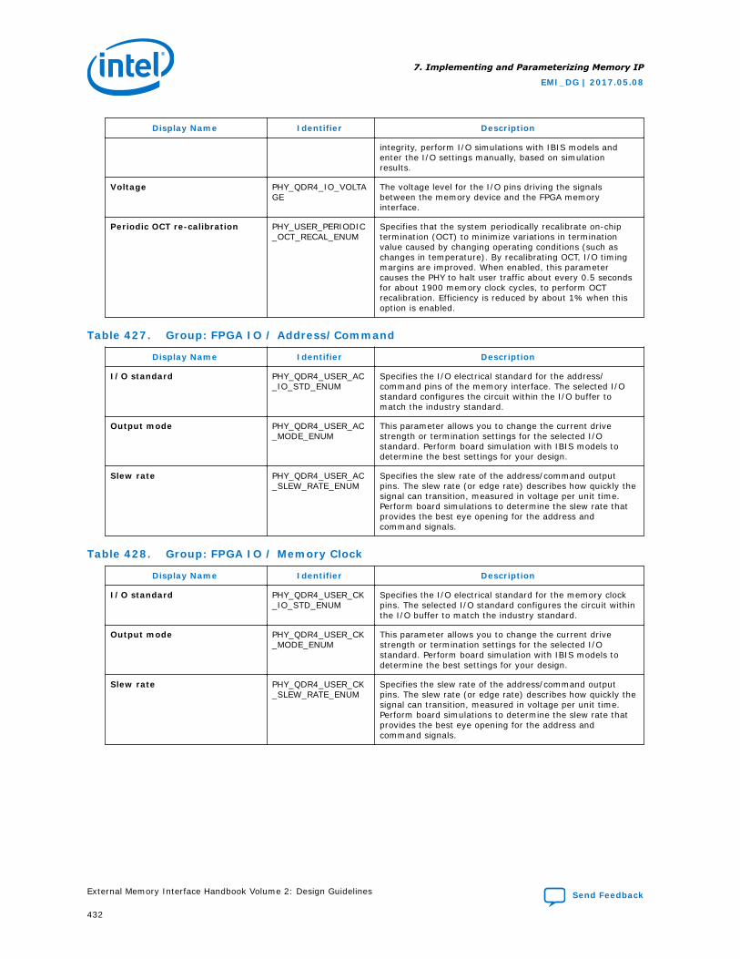
Display Name Identifier Description
integrity, perform I/O simulations with IBIS models andenter the I/O settings manually, based on simulationresults.
Voltage PHY_QDR4_IO_VOLTAGE
The voltage level for the I/O pins driving the signalsbetween the memory device and the FPGA memoryinterface.
Periodic OCT re-calibration PHY_USER_PERIODIC_OCT_RECAL_ENUM
Specifies that the system periodically recalibrate on-chiptermination (OCT) to minimize variations in terminationvalue caused by changing operating conditions (such aschanges in temperature). By recalibrating OCT, I/O timingmargins are improved. When enabled, this parametercauses the PHY to halt user traffic about every 0.5 secondsfor about 1900 memory clock cycles, to perform OCTrecalibration. Efficiency is reduced by about 1% when thisoption is enabled.
Table 427. Group: FPGA IO / Address/Command
Display Name Identifier Description
I/O standard PHY_QDR4_USER_AC_IO_STD_ENUM
Specifies the I/O electrical standard for the address/command pins of the memory interface. The selected I/Ostandard configures the circuit within the I/O buffer tomatch the industry standard.
Output mode PHY_QDR4_USER_AC_MODE_ENUM
This parameter allows you to change the current drivestrength or termination settings for the selected I/Ostandard. Perform board simulation with IBIS models todetermine the best settings for your design.
Slew rate PHY_QDR4_USER_AC_SLEW_RATE_ENUM
Specifies the slew rate of the address/command outputpins. The slew rate (or edge rate) describes how quickly thesignal can transition, measured in voltage per unit time.Perform board simulations to determine the slew rate thatprovides the best eye opening for the address andcommand signals.
Table 428. Group: FPGA IO / Memory Clock
Display Name Identifier Description
I/O standard PHY_QDR4_USER_CK_IO_STD_ENUM
Specifies the I/O electrical standard for the memory clockpins. The selected I/O standard configures the circuit withinthe I/O buffer to match the industry standard.
Output mode PHY_QDR4_USER_CK_MODE_ENUM
This parameter allows you to change the current drivestrength or termination settings for the selected I/Ostandard. Perform board simulation with IBIS models todetermine the best settings for your design.
Slew rate PHY_QDR4_USER_CK_SLEW_RATE_ENUM
Specifies the slew rate of the address/command outputpins. The slew rate (or edge rate) describes how quickly thesignal can transition, measured in voltage per unit time.Perform board simulations to determine the slew rate thatprovides the best eye opening for the address andcommand signals.
7. Implementing and Parameterizing Memory IP
EMI_DG | 2017.05.08
External Memory Interface Handbook Volume 2: Design Guidelines Send Feedback
432

Table 429. Group: FPGA IO / Data Bus
Display Name Identifier Description
Use recommended initial Vrefin PHY_QDR4_USER_AUTO_STARTING_VREFIN_EN
Specifies that the initial Vrefin setting is calculatedautomatically, to a reasonable value based on terminationsettings.
Input mode PHY_QDR4_USER_DATA_IN_MODE_ENUM
This parameter allows you to change the input terminationsettings for the selected I/O standard. Perform boardsimulation with IBIS models to determine the best settingsfor your design.
I/O standard PHY_QDR4_USER_DATA_IO_STD_ENUM
Specifies the I/O electrical standard for the data and dataclock/strobe pins of the memory interface. The selected I/Ostandard option configures the circuit within the I/O bufferto match the industry standard.
Output mode PHY_QDR4_USER_DATA_OUT_MODE_ENUM
This parameter allows you to change the output currentdrive strength or termination settings for the selected I/Ostandard. Perform board simulation with IBIS models todetermine the best settings for your design.
Initial Vrefin PHY_QDR4_USER_STARTING_VREFIN
Specifies the initial value for the reference voltage on thedata pins (Vrefin). This value is entered as a percentage ofthe supply voltage level on the I/O pins. The specified valueserves as a starting point and may be overridden bycalibration to provide better timing margins. If you chooseto skip Vref calibration (Diagnostics tab), this is the valuethat is used as the Vref for the interface.
Table 430. Group: FPGA IO / PHY Inputs
Display Name Identifier Description
PLL reference clock I/Ostandard
PHY_QDR4_USER_PLL_REF_CLK_IO_STD_ENUM
Specifies the I/O standard for the PLL reference clock of thememory interface.
RZQ I/O standard PHY_QDR4_USER_RZQ_IO_STD_ENUM
Specifies the I/O standard for the RZQ pin used in thememory interface.
RZQ resistor PHY_RZQ Specifies the reference resistor used to calibrate the on-chiptermination value. You should connect the RZQ pin to GNDthrough an external resistor of the specified value.
7.5.6.4. Stratix 10 EMIF IP QDR-IV Parameters: Mem Timing
These parameters should be read from the table in the datasheet associated with thespeed bin of the memory device (not necessarily the frequency at which the interfaceis running).
Table 431. Group: Mem Timing / Parameters dependent on Speed Bin
Display Name Identifier Description
Speed bin MEM_QDR4_SPEEDBIN_ENUM
The speed grade of the memory device used. Thisparameter refers to the maximum rate at which thememory device is specified to run.
tASH MEM_QDR4_TASH_PS tASH provides the setup/hold window requirement for theaddress bus in relation to the CK clock. Because theindividual signals in the address bus may not be perfectlyaligned with each other, this parameter describes theintersection window for all the individual address signalssetup/hold margins.
continued...
7. Implementing and Parameterizing Memory IP
EMI_DG | 2017.05.08
Send Feedback External Memory Interface Handbook Volume 2: Design Guidelines
433

Display Name Identifier Description
tCKDK_max MEM_QDR4_TCKDK_MAX_PS
tCKDK_max refers to the maximum skew from the memoryclock (CK) to the write strobe (DK).
tCKDK_min MEM_QDR4_TCKDK_MIN_PS
tCKDK_min refers to the minimum skew from the memoryclock (CK) to the write strobe (DK).
tCKQK_max MEM_QDR4_TCKQK_MAX_PS
tCKQK_max refers to the maximum skew from the memoryclock (CK) to the read strobe (QK).
tCSH MEM_QDR4_TCSH_PS tCSH provides the setup/hold window requirement for thecontrol bus (LD#, RW#) in relation to the CK clock. Becausethe individual signals in the control bus may not be perfectlyaligned with each other, this parameter describes theintersection window for all the individual control signalssetup/hold margins.
tISH MEM_QDR4_TISH_PS tISH provides the setup/hold window requirement for theentire data bus (DK or DINV) in all the data groups withrespect to the DK clock. After deskew calibration, thisparameter describes the intersection window for all theindividual data bus signals setup/hold margins.
tQH MEM_QDR4_TQH_CYC tQH specifies the output hold time for the DQ/DINV inrelation to QK.
tQKQ_max MEM_QDR4_TQKQ_MAX_PS
tQKQ_max describes the maximum skew between the readstrobe (QK) clock edge to the data bus (DQ/DINV) edge.
7.5.6.5. Stratix 10 EMIF IP QDR-IV Parameters: Board
Table 432. Group: Board / Intersymbol Interference/Crosstalk
Display Name Identifier Description
Address and command ISI/crosstalk
BOARD_QDR4_USER_AC_ISI_NS
The address and command window reduction due to ISI andcrosstalk effects. The number to be entered is the total ofthe measured loss of margin on the setup side plus themeasured loss of margin on the hold side. Refer to the EMIFSimulation Guidance wiki page for additional information.
QK/QK# ISI/crosstalk BOARD_QDR4_USER_RCLK_ISI_NS
QK/QK# ISI/crosstalk describes the reduction of the readdata window due to intersymbol interference and crosstalkeffects on the QK/QK# signal when driven by the memorydevice during a read. The number to be entered in theQuartus Prime software is the total of the measured loss ofmargin on the setup side plus the measured loss of marginon the hold side. Refer to the EMIF Simulation Guidancewiki page for additional information.
Read DQ ISI/crosstalk BOARD_QDR4_USER_RDATA_ISI_NS
The reduction of the read data window due to ISI andcrosstalk effects on the DQ signal when driven by thememory device during a read. The number to be entered isthe total of the measured loss of margin on the setup sideplus the measured loss of margin on the hold side. Refer tothe EMIF Simulation Guidance wiki page for additionalinformation.
DK/DK# ISI/crosstalk BOARD_QDR4_USER_WCLK_ISI_NS
DK/DK# ISI/crosstalk describes the reduction of the writedata window due to intersymbol interference and crosstalkeffects on the DK/DK# signal when driven by the FPGAduring a write. The number to be entered in the QuartusPrime software is the total of the measured loss of margin
continued...
7. Implementing and Parameterizing Memory IP
EMI_DG | 2017.05.08
External Memory Interface Handbook Volume 2: Design Guidelines Send Feedback
434
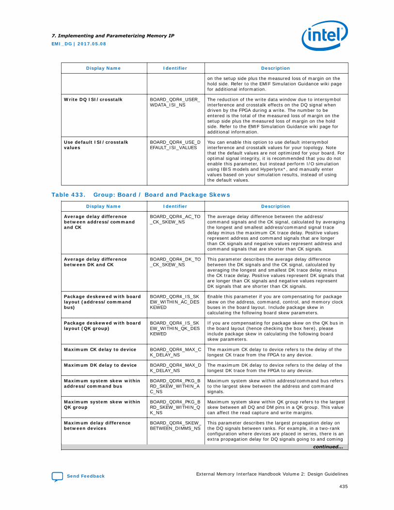
Display Name Identifier Description
on the setup side plus the measured loss of margin on thehold side. Refer to the EMIF Simulation Guidance wiki pagefor additional information.
Write DQ ISI/crosstalk BOARD_QDR4_USER_WDATA_ISI_NS
The reduction of the write data window due to intersymbolinterference and crosstalk effects on the DQ signal whendriven by the FPGA during a write. The number to beentered is the total of the measured loss of margin on thesetup side plus the measured loss of margin on the holdside. Refer to the EMIF Simulation Guidance wiki page foradditional information.
Use default ISI/crosstalkvalues
BOARD_QDR4_USE_DEFAULT_ISI_VALUES
You can enable this option to use default intersymbolinterference and crosstalk values for your topology. Notethat the default values are not optimized for your board. Foroptimal signal integrity, it is recommended that you do notenable this parameter, but instead perform I/O simulationusing IBIS models and Hyperlynx*, and manually entervalues based on your simulation results, instead of usingthe default values.
Table 433. Group: Board / Board and Package Skews
Display Name Identifier Description
Average delay differencebetween address/commandand CK
BOARD_QDR4_AC_TO_CK_SKEW_NS
The average delay difference between the address/command signals and the CK signal, calculated by averagingthe longest and smallest address/command signal tracedelay minus the maximum CK trace delay. Positive valuesrepresent address and command signals that are longerthan CK signals and negative values represent address andcommand signals that are shorter than CK signals.
Average delay differencebetween DK and CK
BOARD_QDR4_DK_TO_CK_SKEW_NS
This parameter describes the average delay differencebetween the DK signals and the CK signal, calculated byaveraging the longest and smallest DK trace delay minusthe CK trace delay. Positive values represent DK signals thatare longer than CK signals and negative values representDK signals that are shorter than CK signals.
Package deskewed with boardlayout (address/commandbus)
BOARD_QDR4_IS_SKEW_WITHIN_AC_DESKEWED
Enable this parameter if you are compensating for packageskew on the address, command, control, and memory clockbuses in the board layout. Include package skew incalculating the following board skew parameters.
Package deskewed with boardlayout (QK group)
BOARD_QDR4_IS_SKEW_WITHIN_QK_DESKEWED
If you are compensating for package skew on the QK bus inthe board layout (hence checking the box here), pleaseinclude package skew in calculating the following boardskew parameters.
Maximum CK delay to device BOARD_QDR4_MAX_CK_DELAY_NS
The maximum CK delay to device refers to the delay of thelongest CK trace from the FPGA to any device.
Maximum DK delay to device BOARD_QDR4_MAX_DK_DELAY_NS
The maximum DK delay to device refers to the delay of thelongest DK trace from the FPGA to any device.
Maximum system skew withinaddress/command bus
BOARD_QDR4_PKG_BRD_SKEW_WITHIN_AC_NS
Maximum system skew within address/command bus refersto the largest skew between the address and commandsignals.
Maximum system skew withinQK group
BOARD_QDR4_PKG_BRD_SKEW_WITHIN_QK_NS
Maximum system skew within QK group refers to the largestskew between all DQ and DM pins in a QK group. This valuecan affect the read capture and write margins.
Maximum delay differencebetween devices
BOARD_QDR4_SKEW_BETWEEN_DIMMS_NS
This parameter describes the largest propagation delay onthe DQ signals between ranks. For example, in a two-rankconfiguration where devices are placed in series, there is anextra propagation delay for DQ signals going to and coming
continued...
7. Implementing and Parameterizing Memory IP
EMI_DG | 2017.05.08
Send Feedback External Memory Interface Handbook Volume 2: Design Guidelines
435
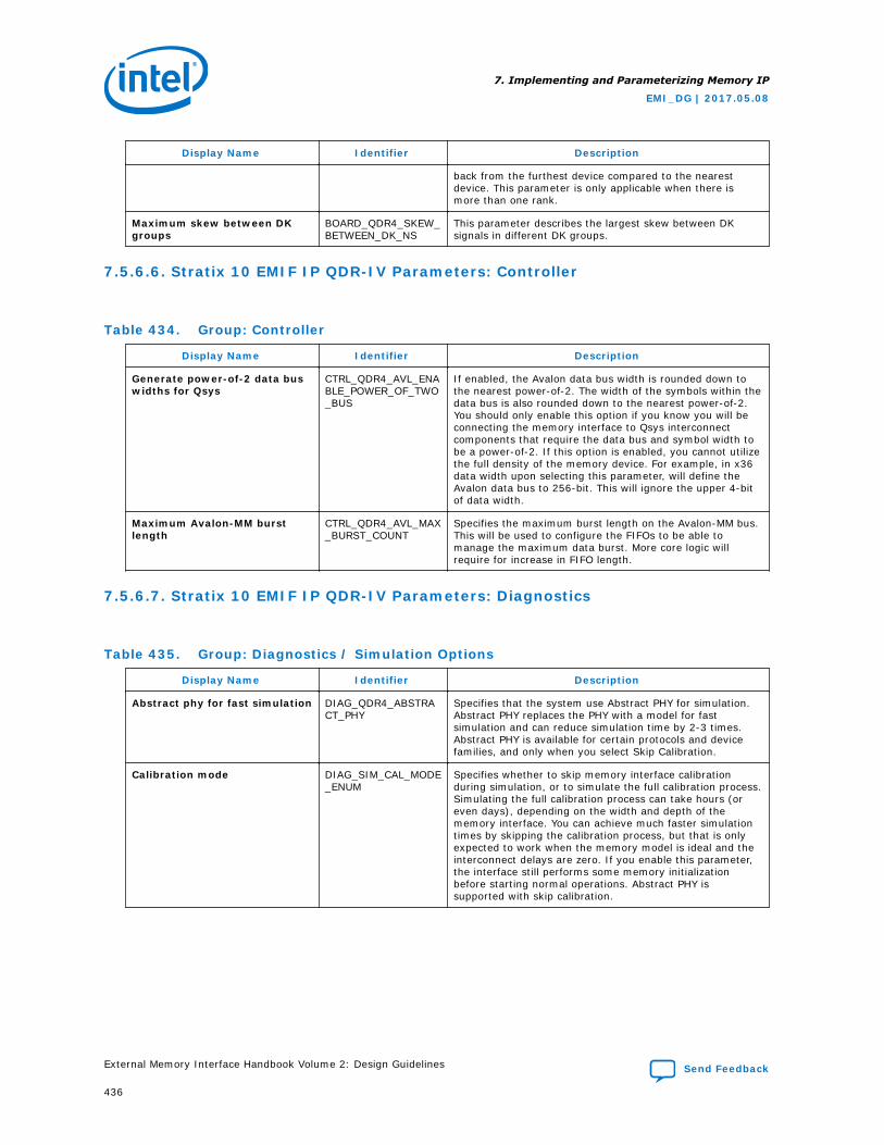
Display Name Identifier Description
back from the furthest device compared to the nearestdevice. This parameter is only applicable when there ismore than one rank.
Maximum skew between DKgroups
BOARD_QDR4_SKEW_BETWEEN_DK_NS
This parameter describes the largest skew between DKsignals in different DK groups.
7.5.6.6. Stratix 10 EMIF IP QDR-IV Parameters: Controller
Table 434. Group: Controller
Display Name Identifier Description
Generate power-of-2 data buswidths for Qsys
CTRL_QDR4_AVL_ENABLE_POWER_OF_TWO_BUS
If enabled, the Avalon data bus width is rounded down tothe nearest power-of-2. The width of the symbols within thedata bus is also rounded down to the nearest power-of-2.You should only enable this option if you know you will beconnecting the memory interface to Qsys interconnectcomponents that require the data bus and symbol width tobe a power-of-2. If this option is enabled, you cannot utilizethe full density of the memory device. For example, in x36data width upon selecting this parameter, will define theAvalon data bus to 256-bit. This will ignore the upper 4-bitof data width.
Maximum Avalon-MM burstlength
CTRL_QDR4_AVL_MAX_BURST_COUNT
Specifies the maximum burst length on the Avalon-MM bus.This will be used to configure the FIFOs to be able tomanage the maximum data burst. More core logic willrequire for increase in FIFO length.
7.5.6.7. Stratix 10 EMIF IP QDR-IV Parameters: Diagnostics
Table 435. Group: Diagnostics / Simulation Options
Display Name Identifier Description
Abstract phy for fast simulation DIAG_QDR4_ABSTRACT_PHY
Specifies that the system use Abstract PHY for simulation.Abstract PHY replaces the PHY with a model for fastsimulation and can reduce simulation time by 2-3 times.Abstract PHY is available for certain protocols and devicefamilies, and only when you select Skip Calibration.
Calibration mode DIAG_SIM_CAL_MODE_ENUM
Specifies whether to skip memory interface calibrationduring simulation, or to simulate the full calibration process.Simulating the full calibration process can take hours (oreven days), depending on the width and depth of thememory interface. You can achieve much faster simulationtimes by skipping the calibration process, but that is onlyexpected to work when the memory model is ideal and theinterconnect delays are zero. If you enable this parameter,the interface still performs some memory initializationbefore starting normal operations. Abstract PHY issupported with skip calibration.
7. Implementing and Parameterizing Memory IP
EMI_DG | 2017.05.08
External Memory Interface Handbook Volume 2: Design Guidelines Send Feedback
436

Table 436. Group: Diagnostics / Calibration Debug Options
Display Name Identifier Description
Enable Daisy-Chaining forQuartus Prime EMIF DebugToolkit/On-Chip Debug Port
DIAG_EXPORT_SEQ_AVALON_MASTER
Specifies that the IP export an Avalon-MM master interface(cal_debug_out) which can connect to the cal_debuginterface of other EMIF cores residing in the same I/Ocolumn. This parameter applies only if the EMIF DebugToolkit or On-Chip Debug Port is enabled. Refer to theDebugging Multiple EMIFs wiki page for more informationabout debugging multiple EMIFs.
Quartus Prime EMIF DebugToolkit/On-Chip Debug Port
DIAG_EXPORT_SEQ_AVALON_SLAVE
Specifies the connectivity of an Avalon slave interface foruse by the Quartus Prime EMIF Debug Toolkit or user corelogic. If you set this parameter to "Disabled," no debugfeatures are enabled. If you set this parameter to "Export,"an Avalon slave interface named "cal_debug" is exportedfrom the IP. To use this interface with the EMIF DebugToolkit, you must instantiate and connect an EMIF debuginterface IP core to it, or connect it to the cal_debug_outinterface of another EMIF core. If you select "Add EMIFDebug Interface", an EMIF debug interface componentcontaining a JTAG Avalon Master is connected to the debugport, allowing the core to be accessed by the EMIF DebugToolkit. Only one EMIF debug interface should beinstantiated per I/O column. You can chain additional EMIFor PHYLite cores to the first by enabling the "Enable Daisy-Chaining for Quartus Prime EMIF Debug Toolkit/On-ChipDebug Port" option for all cores in the chain, and selecting"Export" for the "Quartus Prime EMIF Debug Toolkit/On-ChipDebug Port" option on all cores after the first.
Interface ID DIAG_INTERFACE_ID Identifies interfaces within the I/O column, for use by theEMIF Debug Toolkit and the On-Chip Debug Port. InterfaceIDs should be unique among EMIF cores within the sameI/O column. If the Quartus Prime EMIF Debug Toolkit/On-Chip Debug Port parameter is set to Disabled, the interfaceID is unused.
Skip VREF_in calibration DIAG_QDR4_SKIP_VREF_CAL
Users can check this option to skip the VREF stage ofcalibration. Users should enable this option for debugpurpose only; it is recommended to keep enabled duringnormal opertation.
Use Soft NIOS Processor forOn-Chip Debug
DIAG_SOFT_NIOS_MODE
Enables a soft Nios processor as a peripheral component toaccess the On-Chip Debug Port. Only one interface in acolumn can activate this option.
Table 437. Group: Diagnostics / Example Design
Display Name Identifier Description
Enable In-System-Sources-and-Probes
DIAG_EX_DESIGN_ISSP_EN
Enables In-System-Sources-and-Probes in the exampledesign for common debug signals, such as calibration statusor example traffic generator per-bit status. This parametermust be enabled if you want to do driver margining.
Number of core clocks sharingslaves to instantiate in theexample design
DIAG_EX_DESIGN_NUM_OF_SLAVES
Specifies the number of core clock sharing slaves toinstantiate in the example design. This parameter appliesonly if you set the "Core clocks sharing" parameter in the"General" tab to Master or Slave.
7. Implementing and Parameterizing Memory IP
EMI_DG | 2017.05.08
Send Feedback External Memory Interface Handbook Volume 2: Design Guidelines
437
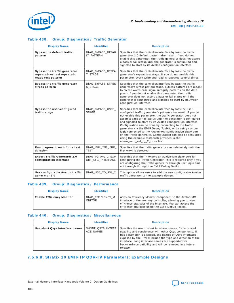
Table 438. Group: Diagnostics / Traffic Generator
Display Name Identifier Description
Bypass the default trafficpattern
DIAG_BYPASS_DEFAULT_PATTERN
Specifies that the controller/interface bypass the trafficgenerator 2.0 default pattern after reset. If you do notenable this parameter, the traffic generator does not asserta pass or fail status until the generator is configured andsignaled to start by its Avalon configuration interface.
Bypass the traffic generatorrepeated-writes/repeated-reads test pattern
DIAG_BYPASS_REPEAT_STAGE
Specifies that the controller/interface bypass the trafficgenerator's repeat test stage. If you do not enable thisparameter, every write and read is repeated several times.
Bypass the traffic generatorstress pattern
DIAG_BYPASS_STRESS_STAGE
Specifies that the controller/interface bypass the trafficgenerator's stress pattern stage. (Stress patterns are meantto create worst-case signal integrity patterns on the datapins.) If you do not enable this parameter, the trafficgenerator does not assert a pass or fail status until thegenerator is configured and signaled to start by its Avalonconfiguration interface.
Bypass the user-configuredtraffic stage
DIAG_BYPASS_USER_STAGE
Specifies that the controller/interface bypass the user-configured traffic generator's pattern after reset. If you donot enable this parameter, the traffic generator does notassert a pass or fail status until the generator is configuredand signaled to start by its Avalon configuration interface.Configuration can be done by connecting to the trafficgenerator via the EMIF Debug Toolkit, or by using customlogic connected to the Avalon-MM configuration slave porton the traffic generator. Configuration can also be simulatedusing the example testbench provided in thealtera_emif_avl_tg_2_tb.sv file.
Run diagnostic on infinite testduration
DIAG_INFI_TG2_ERR_TEST
Specifies that the traffic generator run indefinitely until thefirst error is detected.
Export Traffic Generator 2.0configuration interface
DIAG_TG_AVL_2_EXPORT_CFG_INTERFACE
Specifies that the IP export an Avalon-MM slave port forconfiguring the Traffic Generator. This is required only if youare configuring the traffic generator through user logic andnot through through the EMIF Debug Toolkit.
Use configurable Avalon trafficgenerator 2.0
DIAG_USE_TG_AVL_2 This option allows users to add the new configurable Avalontraffic generator to the example design.
Table 439. Group: Diagnostics / Performance
Display Name Identifier Description
Enable Efficiency Monitor DIAG_EFFICIENCY_MONITOR
Adds an Efficiency Monitor component to the Avalon-MMinterface of the memory controller, allowing you to viewefficiency statistics of the interface. You can access theefficiency statistics using the EMIF Debug Toolkit.
Table 440. Group: Diagnostics / Miscellaneous
Display Name Identifier Description
Use short Qsys interface names SHORT_QSYS_INTERFACE_NAMES
Specifies the use of short interface names, for improvedusability and consistency with other Qsys components. Ifthis parameter is disabled, the names of Qsys interfacesexposed by the IP will include the type and direction of theinterface. Long interface names are supported forbackward-compatibility and will be removed in a futurerelease.
7.5.6.8. Stratix 10 EMIF IP QDR-IV Parameters: Example Designs
7. Implementing and Parameterizing Memory IP
EMI_DG | 2017.05.08
External Memory Interface Handbook Volume 2: Design Guidelines Send Feedback
438

Table 441. Group: Example Designs / Available Example Designs
Display Name Identifier Description
Select design EX_DESIGN_GUI_QDR4_SEL_DESIGN
Specifies the creation of a full Quartus Prime project,instantiating an external memory interface and an exampletraffic generator, according to your parameterization. Afterthe design is created, you can specify the target device andpin location assignments, run a full compilation, verifytiming closure, and test the interface on your board usingthe programming file created by the Quartus Primeassembler. The 'Generate Example Design' button lets yougenerate simulation or synthesis file sets.
Table 442. Group: Example Designs / Example Design Files
Display Name Identifier Description
Simulation EX_DESIGN_GUI_QDR4_GEN_SIM
Specifies that the 'Generate Example Design' button createall necessary file sets for simulation. Expect a shortadditional delay as the file set is created. If you do notenable this parameter, simulation file sets are not created.Instead, the output directory will contain the ed_sim.qsysfile which holds Qsys details of the simulation exampledesign, and a make_sim_design.tcl file with othercorresponding tcl files. You can run make_sim_design.tclfrom a command line to generate the simulation exampledesign. The generated example designs for varioussimulators are stored in the /sim sub-directory.
Synthesis EX_DESIGN_GUI_QDR4_GEN_SYNTH
Specifies that the 'Generate Example Design' button createall necessary file sets for synthesis. Expect a shortadditional delay as the file set is created. If you do notenable this parameter, synthesis file sets are not created.Instead, the output directory will contain the ed_synth.qsysfile which holds Qsys details of the synthesis exampledesign, and a make_qii_design.tcl script with othercorresponding tcl files. You can run make_qii_design.tclfrom a command line to generate the synthesis exampledesign. The generated example design is stored in the /qiisub-directory.
Table 443. Group: Example Designs / Generated HDL Format
Display Name Identifier Description
Simulation HDL format EX_DESIGN_GUI_QDR4_HDL_FORMAT
This option lets you choose the format of HDL in whichgenerated simulation files are created.
Table 444. Group: Example Designs / Target Development Kit
Display Name Identifier Description
Select board EX_DESIGN_GUI_QDR4_TARGET_DEV_KIT
Specifies that when you select a development kit with amemory module, the generated example design contains allsettings and fixed pin assignments to run on the selectedboard. You must select a development kit preset togenerate a working example design for the specifieddevelopment kit. Any IP settings not applied directly from adevelopment kit preset will not have guaranteed resultswhen testing the development kit. To exclude hardwaresupport of the example design, select 'none' from the'Select board' pull down menu. When you apply adevelopment kit preset, all IP parameters are automaticallyset appropriately to match the selected preset. If you wantto save your current settings, you should do so before youapply the preset. You can save your settings under adifferent name using File->Save as.
7. Implementing and Parameterizing Memory IP
EMI_DG | 2017.05.08
Send Feedback External Memory Interface Handbook Volume 2: Design Guidelines
439
7.5.6.9. About Memory Presets
Presets help simplify the process of copying memory parameter values from memorydevice data sheets to the EMIF parameter editor.
For DDRx protocols, the memory presets are named using the following convention:
PROTOCOL-SPEEDBIN LATENCY FORMAT-AND-TOPOLOGY CAPACITY (INTERNAL-ORGANIZATION)
For example, the preset named DDR4-2666U CL18 Component 1CS 2Gb (512Mbx 4) refers to a DDR4 x4 component rated at the DDR4-2666U JEDEC speed bin, withnominal CAS latency of 18 cycles, one chip-select, and a total memory space of 2Gb.The JEDEC memory specification defines multiple speed bins for a given frequency(that is, DDR4-2666U and DDR4-2666V). You may be able to determine the exactspeed bin implemented by your memory device using its nominal latency. When indoubt, contact your memory vendor.
For RLDRAMx and QDRx protocols, the memory presets are named based on thevendor's device part number.
When the preset list does not contain the exact configuration required, you can stillminimize data entry by selecting the preset closest to your configuration and thenmodify parameters as required.
Prior to production you should always review the parameter values to ensure that theymatch your memory device data sheet, regardless of whether a preset is used or not.Incorrect memory parameters can cause functional failures.
7.5.7. Stratix 10 EMIF IP QDR II/II+/II+ Xtreme Parameters
The Stratix 10 EMIF IP parameter editor allows you to parameterize settings for theStratix 10 EMIF IP.
The text window at the bottom of the parameter editor displays information about thememory interface, as well as warning and error messages. You should correct anyerrors indicated in this window before clicking the Finish button.
Note: Default settings are the minimum required to achieve timing, and may vary dependingon memory protocol.
The following tables describe the parameterization settings available in the parametereditor for the Stratix 10 EMIF IP.
7.5.7.1. Stratix 10 EMIF IP QDR II/II+/II+ Xtreme Parameters: General
Table 445. Group: General / FPGA
Display Name Identifier Description
Speed grade PHY_FPGA_SPEEDGRADE_GUI
Indicates the device speed grade, and whether it is anengineering sample (ES) or production device. This value isbased on the device that you select in the parameter editor.If you do not specify a device, the system assumes adefault value. Ensure that you always specify the correctdevice during IP generation, otherwise your IP may notwork in hardware.
7. Implementing and Parameterizing Memory IP
EMI_DG | 2017.05.08
External Memory Interface Handbook Volume 2: Design Guidelines Send Feedback
440

Table 446. Group: General / Interface
Display Name Identifier Description
Configuration PHY_CONFIG_ENUM Specifies the configuration of the memory interface. Theavailable options depend on the protocol in use. Optionsinclude Hard PHY and Hard Controller, Hard PHY and SoftController, or Hard PHY only. If you select Hard PHY only,the AFI interface is exported to allow connection of acustom memory controller or third-party IP.
Instantiate two controllerssharing a Ping Pong PHY
PHY_PING_PONG_EN Specifies the instantiation of two identical memorycontrollers that share an address/command bus through theuse of Ping Pong PHY. This parameter is available only if youspecify the Hard PHY and Hard Controller option. When thisparameter is enabled, the IP exposes two independentAvalon interfaces to the user logic, and a single externalmemory interface with double width for the data bus andthe CS#, CKE, ODT, and CK/CK# signals.
Table 447. Group: General / Clocks
Display Name Identifier Description
Core clocks sharing PHY_CORE_CLKS_SHARING_ENUM
When a design contains multiple interfaces of the sameprotocol, rate, frequency, and PLL reference clock source,they can share a common set of core clock domains. Bysharing core clock domains, they reduce clock networkusage and avoid clock synchronization logic between theinterfaces. To share core clocks, denote one of theinterfaces as "Master", and the remaining interfaces as"Slave". In the RTL, connect the clks_sharing_master_outsignal from the master interface to theclks_sharing_slave_in signal of all the slave interfaces. Bothmaster and slave interfaces still expose their own outputclock ports in the RTL (for example, emif_usr_clk, afi_clk),but the physical signals are equivalent, hence it does notmatter whether a clock port from a master or a slave isused. As the combined width of all interfaces sharing thesame core clock increases, you may encounter timingclosure difficulty for transfers between the FPGA core andthe periphery.
Memory clock frequency PHY_MEM_CLK_FREQ_MHZ
Specifies the operating frequency of the memory interfacein MHz. If you change the memory frequency, you shouldupdate the memory latency parameters on the "Memory"tab and the memory timing parameters on the "MemTiming" tab.
Use recommended PLLreference clock frequency
PHY_QDR2_DEFAULT_REF_CLK_FREQ
Specifies that the PLL reference clock frequency isautomatically calculated for best performance. If you wantto specify a different PLL reference clock frequency, uncheckthe check box for this parameter.
Clock rate of user logic PHY_RATE_ENUM Specifies the relationship between the user logic clockfrequency and the memory clock frequency. For example, ifthe memory clock sent from the FPGA to the memorydevice is toggling at 800MHz, a quarter-rate interfacemeans that the user logic in the FPGA runs at 200MHz.
PLL reference clock frequency PHY_REF_CLK_FREQ_MHZ
Specifies the PLL reference clock frequency. You mustconfigure this parameter only if you do not check the "Userecommended PLL reference clock frequency" parameter. Toconfigure this parameter, select a valid PLL reference clockfrequency from the list. The values in the list can change ifyou change the memory interface frequency and/or the
continued...
7. Implementing and Parameterizing Memory IP
EMI_DG | 2017.05.08
Send Feedback External Memory Interface Handbook Volume 2: Design Guidelines
441

Display Name Identifier Description
clock rate of the user logic. For best jitter performance, youshould use the fastest possible PLL reference clockfrequency.
PLL reference clock jitter PHY_REF_CLK_JITTER_PS
Specifies the peak-to-peak jitter on the PLL reference clocksource. The clock source of the PLL reference clock mustmeet or exceed the following jitter requirements: 10ps peakto peak, or 1.42ps RMS at 1e-12 BER, 1.22ps at 1e-16 BER.
Specify additional core clocksbased on existing PLL
PLL_ADD_EXTRA_CLKS
Displays additional parameters allowing you to createadditional output clocks based on the existing PLL. Thisparameter provides an alternative clock-generationmechanism for when your design exhausts available PLLresources. The additional output clocks that you create canbe fed into the core. Clock signals created with thisparameter are synchronous to each other, but asynchronousto the memory interface core clock domains (such asemif_usr_clk or afi_clk). You must follow proper clock-domain-crossing techniques when transferring data betweenclock domains.
Table 448. Group: General / Additional Core Clocks
Display Name Identifier Description
Number of additional coreclocks
PLL_USER_NUM_OF_EXTRA_CLKS
Specifies the number of additional output clocks to createfrom the PLL.
7.5.7.2. Stratix 10 EMIF IP QDR II/II+/II+ Xtreme Parameters: Memory
Table 449. Group: Memory / Topology
Display Name Identifier Description
Address width MEM_QDR2_ADDR_WIDTH
Number of address pins.
Burst length MEM_QDR2_BL Burst length of the memory device.
Enable BWS# pins MEM_QDR2_BWS_EN Indicates whether the interface uses the BWS#( Byte WriteSelect) pins. If enabled, 1 BWS# pin for every 9 D pins willbe added.
BWS# width MEM_QDR2_BWS_N_WIDTH
Number of BWS# (Byte Write Select) pins of the memoryinterface. Automatically calculated based on the data widthper device and whether width expansion is enabled. BWS#pins are used to select which byte is written into the deviceduring the current portion of the write operations. Bytes notwritten remain unaltered.
CQ width MEM_QDR2_CQ_WIDTH
Width of the CQ (read strobe) clock on the memory device.
Data width per device MEM_QDR2_DATA_PER_DEVICE
Number of D and Q pins per QDR II device.
continued...
7. Implementing and Parameterizing Memory IP
EMI_DG | 2017.05.08
External Memory Interface Handbook Volume 2: Design Guidelines Send Feedback
442

Display Name Identifier Description
Data width MEM_QDR2_DATA_WIDTH
Number of D and Q pins of the memory interface.Automatically calculated based on the D and Q width perdevice and whether width expansion is enabled.
K width MEM_QDR2_K_WIDTH Width of the K (address, command and write strobe) clockon the memory device.
Enable width expansion MEM_QDR2_WIDTH_EXPANDED
Indicates whether to combine two memory devices todouble the data bus width. With two devices, the interfacesupports a width expansion configuration up to 72-bits. Forwidth expansion configuration, the address and controlsignals are routed to 2 devices.
7.5.7.3. Stratix 10 EMIF IP QDR II/II+/II+ Xtreme Parameters: FPGA I/O
You should use Hyperlynx* or similar simulators to determine the best settings foryour board. Refer to the EMIF Simulation Guidance wiki page for additionalinformation.
Table 450. Group: FPGA IO / FPGA IO Settings
Display Name Identifier Description
Use default I/O settings PHY_QDR2_DEFAULT_IO
Specifies that a legal set of I/O settings are automaticallyselected. The default I/O settings are not necessarilyoptimized for a specific board. To achieve optimal signalintegrity, perform I/O simulations with IBIS models andenter the I/O settings manually, based on simulationresults.
Voltage PHY_QDR2_IO_VOLTAGE
The voltage level for the I/O pins driving the signalsbetween the memory device and the FPGA memoryinterface.
Periodic OCT re-calibration PHY_USER_PERIODIC_OCT_RECAL_ENUM
Specifies that the system periodically recalibrate on-chiptermination (OCT) to minimize variations in terminationvalue caused by changing operating conditions (such aschanges in temperature). By recalibrating OCT, I/O timingmargins are improved. When enabled, this parametercauses the PHY to halt user traffic about every 0.5 secondsfor about 1900 memory clock cycles, to perform OCTrecalibration. Efficiency is reduced by about 1% when thisoption is enabled.
Table 451. Group: FPGA IO / Address/Command
Display Name Identifier Description
I/O standard PHY_QDR2_USER_AC_IO_STD_ENUM
Specifies the I/O electrical standard for the address/command pins of the memory interface. The selected I/Ostandard configures the circuit within the I/O buffer tomatch the industry standard.
Output mode PHY_QDR2_USER_AC_MODE_ENUM
This parameter allows you to change the current drivestrength or termination settings for the selected I/Ostandard. Perform board simulation with IBIS models todetermine the best settings for your design.
Slew rate PHY_QDR2_USER_AC_SLEW_RATE_ENUM
Specifies the slew rate of the address/command outputpins. The slew rate (or edge rate) describes how quickly thesignal can transition, measured in voltage per unit time.Perform board simulations to determine the slew rate thatprovides the best eye opening for the address andcommand signals.
7. Implementing and Parameterizing Memory IP
EMI_DG | 2017.05.08
Send Feedback External Memory Interface Handbook Volume 2: Design Guidelines
443

Table 452. Group: FPGA IO / Memory Clock
Display Name Identifier Description
I/O standard PHY_QDR2_USER_CK_IO_STD_ENUM
Specifies the I/O electrical standard for the memory clockpins. The selected I/O standard configures the circuit withinthe I/O buffer to match the industry standard.
Output mode PHY_QDR2_USER_CK_MODE_ENUM
This parameter allows you to change the current drivestrength or termination settings for the selected I/Ostandard. Perform board simulation with IBIS models todetermine the best settings for your design.
Slew rate PHY_QDR2_USER_CK_SLEW_RATE_ENUM
Specifies the slew rate of the address/command outputpins. The slew rate (or edge rate) describes how quickly thesignal can transition, measured in voltage per unit time.Perform board simulations to determine the slew rate thatprovides the best eye opening for the address andcommand signals.
Table 453. Group: FPGA IO / Data Bus
Display Name Identifier Description
Use recommended initial Vrefin PHY_QDR2_USER_AUTO_STARTING_VREFIN_EN
Specifies that the initial Vrefin setting is calculatedautomatically, to a reasonable value based on terminationsettings.
Input mode PHY_QDR2_USER_DATA_IN_MODE_ENUM
This parameter allows you to change the input terminationsettings for the selected I/O standard. Perform boardsimulation with IBIS models to determine the best settingsfor your design.
I/O standard PHY_QDR2_USER_DATA_IO_STD_ENUM
Specifies the I/O electrical standard for the data and dataclock/strobe pins of the memory interface. The selected I/Ostandard option configures the circuit within the I/O bufferto match the industry standard.
Output mode PHY_QDR2_USER_DATA_OUT_MODE_ENUM
This parameter allows you to change the output currentdrive strength or termination settings for the selected I/Ostandard. Perform board simulation with IBIS models todetermine the best settings for your design.
Initial Vrefin PHY_QDR2_USER_STARTING_VREFIN
Specifies the initial value for the reference voltage on thedata pins (Vrefin). This value is entered as a percentage ofthe supply voltage level on the I/O pins. The specified valueserves as a starting point and may be overridden bycalibration to provide better timing margins. If you chooseto skip Vref calibration (Diagnostics tab), this is the valuethat is used as the Vref for the interface.
Table 454. Group: FPGA IO / PHY Inputs
Display Name Identifier Description
PLL reference clock I/Ostandard
PHY_QDR2_USER_PLL_REF_CLK_IO_STD_ENUM
Specifies the I/O standard for the PLL reference clock of thememory interface.
RZQ I/O standard PHY_QDR2_USER_RZQ_IO_STD_ENUM
Specifies the I/O standard for the RZQ pin used in thememory interface.
RZQ resistor PHY_RZQ Specifies the reference resistor used to calibrate the on-chiptermination value. You should connect the RZQ pin to GNDthrough an external resistor of the specified value.
7. Implementing and Parameterizing Memory IP
EMI_DG | 2017.05.08
External Memory Interface Handbook Volume 2: Design Guidelines Send Feedback
444
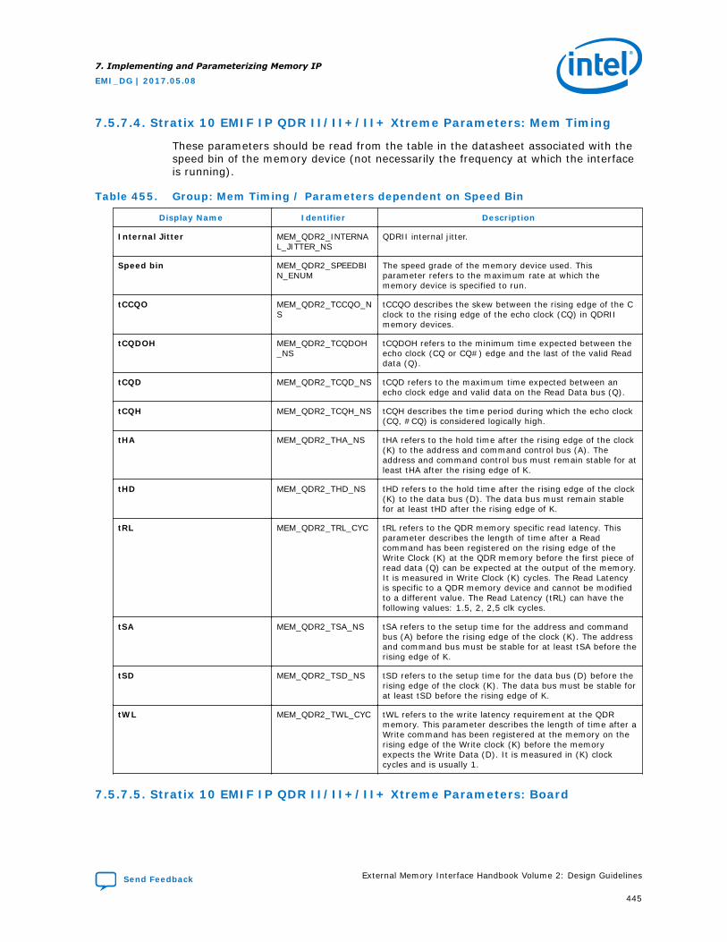
7.5.7.4. Stratix 10 EMIF IP QDR II/II+/II+ Xtreme Parameters: Mem Timing
These parameters should be read from the table in the datasheet associated with thespeed bin of the memory device (not necessarily the frequency at which the interfaceis running).
Table 455. Group: Mem Timing / Parameters dependent on Speed Bin
Display Name Identifier Description
Internal Jitter MEM_QDR2_INTERNAL_JITTER_NS
QDRII internal jitter.
Speed bin MEM_QDR2_SPEEDBIN_ENUM
The speed grade of the memory device used. Thisparameter refers to the maximum rate at which thememory device is specified to run.
tCCQO MEM_QDR2_TCCQO_NS
tCCQO describes the skew between the rising edge of the Cclock to the rising edge of the echo clock (CQ) in QDRIImemory devices.
tCQDOH MEM_QDR2_TCQDOH_NS
tCQDOH refers to the minimum time expected between theecho clock (CQ or CQ#) edge and the last of the valid Readdata (Q).
tCQD MEM_QDR2_TCQD_NS tCQD refers to the maximum time expected between anecho clock edge and valid data on the Read Data bus (Q).
tCQH MEM_QDR2_TCQH_NS tCQH describes the time period during which the echo clock(CQ, #CQ) is considered logically high.
tHA MEM_QDR2_THA_NS tHA refers to the hold time after the rising edge of the clock(K) to the address and command control bus (A). Theaddress and command control bus must remain stable for atleast tHA after the rising edge of K.
tHD MEM_QDR2_THD_NS tHD refers to the hold time after the rising edge of the clock(K) to the data bus (D). The data bus must remain stablefor at least tHD after the rising edge of K.
tRL MEM_QDR2_TRL_CYC tRL refers to the QDR memory specific read latency. Thisparameter describes the length of time after a Readcommand has been registered on the rising edge of theWrite Clock (K) at the QDR memory before the first piece ofread data (Q) can be expected at the output of the memory.It is measured in Write Clock (K) cycles. The Read Latencyis specific to a QDR memory device and cannot be modifiedto a different value. The Read Latency (tRL) can have thefollowing values: 1.5, 2, 2,5 clk cycles.
tSA MEM_QDR2_TSA_NS tSA refers to the setup time for the address and commandbus (A) before the rising edge of the clock (K). The addressand command bus must be stable for at least tSA before therising edge of K.
tSD MEM_QDR2_TSD_NS tSD refers to the setup time for the data bus (D) before therising edge of the clock (K). The data bus must be stable forat least tSD before the rising edge of K.
tWL MEM_QDR2_TWL_CYC tWL refers to the write latency requirement at the QDRmemory. This parameter describes the length of time after aWrite command has been registered at the memory on therising edge of the Write clock (K) before the memoryexpects the Write Data (D). It is measured in (K) clockcycles and is usually 1.
7.5.7.5. Stratix 10 EMIF IP QDR II/II+/II+ Xtreme Parameters: Board
7. Implementing and Parameterizing Memory IP
EMI_DG | 2017.05.08
Send Feedback External Memory Interface Handbook Volume 2: Design Guidelines
445

Table 456. Group: Board / Intersymbol Interference/Crosstalk
Display Name Identifier Description
Address and command ISI/crosstalk
BOARD_QDR2_USER_AC_ISI_NS
The address and command window reduction due to ISI andcrosstalk effects. The number to be entered is the total ofthe measured loss of margin on the setup side plus themeasured loss of margin on the hold side. Refer to the EMIFSimulation Guidance wiki page for additional information.
CQ/CQ# ISI/crosstalk BOARD_QDR2_USER_RCLK_ISI_NS
CQ/CQ# ISI/crosstalk describes the reduction of the readdata window due to intersymbol interference and crosstalkeffects on the CQ/CQ# signal when driven by the memorydevice during a read. The number to be entered in theQuartus Prime software is the total of the measured loss ofmargin on the setup side plus the measured loss of marginon the hold side. Refer to the EMIF Simulation Guidancewiki page for additional information.
Read Q ISI/crosstalk BOARD_QDR2_USER_RDATA_ISI_NS
Read Q ISI/crosstalk describes the reduction of the readdata window due to intersymbol interference and crosstalkeffects on the CQ/CQ# signal when driven by the memorydevice during a read. The number to be entered in theQuartus Prime software is the total of the measured loss ofmargin on the setup side plus the measured loss of marginon the hold side. Refer to the EMIF Simulation Guidancewiki page for additional information.
K/K# ISI/crosstalk BOARD_QDR2_USER_WCLK_ISI_NS
K/K# ISI/crosstalk describes the reduction of the write datawindow due to intersymbol interference and crosstalkeffects on the K/K# signal when driven by the FPGA duringa write. The number to be entered in the Quartus Primesoftware is the total of the measured loss of margin on thesetup side plus the measured loss of margin on the holdside. Refer to the EMIF Simulation Guidance wiki page foradditional information.
Write D ISI/crosstalk BOARD_QDR2_USER_WDATA_ISI_NS
Write D ISI/crosstalk describes the reduction of the writedata window due to intersymbol interference and crosstalkeffects on the signal when driven by driven by the FPGAduring a write. The number to be entered in the QuartusPrime software is the total of the measured loss of marginon the setup side plus the measured loss of margin on thehold side. Refer to the EMIF Simulation Guidance wiki pagefor additional information.
Use default ISI/crosstalkvalues
BOARD_QDR2_USE_DEFAULT_ISI_VALUES
You can enable this option to use default intersymbolinterference and crosstalk values for your topology. Notethat the default values are not optimized for your board. Foroptimal signal integrity, it is recommended that you do notenable this parameter, but instead perform I/O simulationusing IBIS models and Hyperlynx*, and manually entervalues based on your simulation results, instead of usingthe default values.
Table 457. Group: Board / Board and Package Skews
Display Name Identifier Description
Average delay differencebetween address/commandand K
BOARD_QDR2_AC_TO_K_SKEW_NS
This parameter refers to the average delay differencebetween the Address/Command signals and the K signal,calculated by averaging the longest and smallest Address/Command trace delay minus the maximum K trace delay.Positive values represent address and command signals that
continued...
7. Implementing and Parameterizing Memory IP
EMI_DG | 2017.05.08
External Memory Interface Handbook Volume 2: Design Guidelines Send Feedback
446

Display Name Identifier Description
are longer than K signals and negative values representaddress and command signals that are shorter than Ksignals.
Maximum board skew within Dgroup
BOARD_QDR2_BRD_SKEW_WITHIN_D_NS
This parameter refers to the largest skew between all D andBWS# signals in a D group. D pins are used for driving datasignals to the memory device during a write operation.BWS# pins are used as Byte Write Select signals to controlwhich byte(s) are written to the memory during a writeoperation. Users should enter their board skew only.Package skew will be calculated automatically, based on thememory interface configuration, and added to this value.This value affects the read capture and write margins.a
Maximum board skew within Qgroup
BOARD_QDR2_BRD_SKEW_WITHIN_Q_NS
This parameter describes the largest skew between all Qsignals in a Q group. Q pins drive the data signals from thememory to the FPGA when the read operation is active.Users should enter their board skew only. Package skew willbe calculated automatically, based on the memory interfaceconfiguration, and added to this value. This value affects theread capture and write margins.
Package deskewed with boardlayout (address/commandbus)
BOARD_QDR2_IS_SKEW_WITHIN_AC_DESKEWED
Enable this parameter if you are compensating for packageskew on the address, command, control, and memory clockbuses in the board layout. Include package skew incalculating the following board skew parameters.
Package deskewed with boardlayout (D group)
BOARD_QDR2_IS_SKEW_WITHIN_D_DESKEWED
If you are compensating for package skew on the D andBWS# signals in the board layout (hence checking the boxhere), please include package skew in calculating thefollowing board skew parameters.
Package deskewed with boardlayout (Q group)
BOARD_QDR2_IS_SKEW_WITHIN_Q_DESKEWED
If you are compensating for package skew on the Q bus inthe board layout (hence checking the box here), pleaseinclude package skew in calculating the following boardskew parameters.
Maximum K delay to device BOARD_QDR2_MAX_K_DELAY_NS
The maximum K delay to device refers to the delay of thelongest K trace from the FPGA to any device
Maximum system skew withinaddress/command bus
BOARD_QDR2_PKG_BRD_SKEW_WITHIN_AC_NS
Maximum system skew within address/command bus refersto the largest skew between the address and commandsignals.
7.5.7.6. Stratix 10 EMIF IP QDR II/II+/II+ Xtreme Parameters: Controller
Table 458. Group: Controller
Display Name Identifier Description
Generate power-of-2 data buswidths for Qsys
CTRL_QDR2_AVL_ENABLE_POWER_OF_TWO_BUS
If enabled, the Avalon data bus width is rounded down tothe nearest power-of-2. The width of the symbols within thedata bus is also rounded down to the nearest power-of-2.You should only enable this option if you know you will beconnecting the memory interface to Qsys interconnectcomponents that require the data bus and symbol width tobe a power-of-2. If this option is enabled, you cannot utilizethe full density of the memory device. For example, in x36data width upon selecting this parameter, will define theAvalon data bus to 256-bit. This will ignore the upper 4-bitof data width.
Maximum Avalon-MM burstlength
CTRL_QDR2_AVL_MAX_BURST_COUNT
Specifies the maximum burst length on the Avalon-MM bus.This will be used to configure the FIFOs to be able tomanage the maximum data burst. More core logic willrequire for increase in FIFO length.
7. Implementing and Parameterizing Memory IP
EMI_DG | 2017.05.08
Send Feedback External Memory Interface Handbook Volume 2: Design Guidelines
447
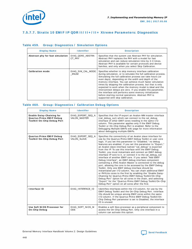
7.5.7.7. Stratix 10 EMIF IP QDR II/II+/II+ Xtreme Parameters: Diagnostics
Table 459. Group: Diagnostics / Simulation Options
Display Name Identifier Description
Abstract phy for fast simulation DIAG_QDR2_ABSTRACT_PHY
Specifies that the system use Abstract PHY for simulation.Abstract PHY replaces the PHY with a model for fastsimulation and can reduce simulation time by 2-3 times.Abstract PHY is available for certain protocols and devicefamilies, and only when you select Skip Calibration.
Calibration mode DIAG_SIM_CAL_MODE_ENUM
Specifies whether to skip memory interface calibrationduring simulation, or to simulate the full calibration process.Simulating the full calibration process can take hours (oreven days), depending on the width and depth of thememory interface. You can achieve much faster simulationtimes by skipping the calibration process, but that is onlyexpected to work when the memory model is ideal and theinterconnect delays are zero. If you enable this parameter,the interface still performs some memory initializationbefore starting normal operations. Abstract PHY issupported with skip calibration.
Table 460. Group: Diagnostics / Calibration Debug Options
Display Name Identifier Description
Enable Daisy-Chaining forQuartus Prime EMIF DebugToolkit/On-Chip Debug Port
DIAG_EXPORT_SEQ_AVALON_MASTER
Specifies that the IP export an Avalon-MM master interface(cal_debug_out) which can connect to the cal_debuginterface of other EMIF cores residing in the same I/Ocolumn. This parameter applies only if the EMIF DebugToolkit or On-Chip Debug Port is enabled. Refer to theDebugging Multiple EMIFs wiki page for more informationabout debugging multiple EMIFs.
Quartus Prime EMIF DebugToolkit/On-Chip Debug Port
DIAG_EXPORT_SEQ_AVALON_SLAVE
Specifies the connectivity of an Avalon slave interface foruse by the Quartus Prime EMIF Debug Toolkit or user corelogic. If you set this parameter to "Disabled," no debugfeatures are enabled. If you set this parameter to "Export,"an Avalon slave interface named "cal_debug" is exportedfrom the IP. To use this interface with the EMIF DebugToolkit, you must instantiate and connect an EMIF debuginterface IP core to it, or connect it to the cal_debug_outinterface of another EMIF core. If you select "Add EMIFDebug Interface", an EMIF debug interface componentcontaining a JTAG Avalon Master is connected to the debugport, allowing the core to be accessed by the EMIF DebugToolkit. Only one EMIF debug interface should beinstantiated per I/O column. You can chain additional EMIFor PHYLite cores to the first by enabling the "Enable Daisy-Chaining for Quartus Prime EMIF Debug Toolkit/On-ChipDebug Port" option for all cores in the chain, and selecting"Export" for the "Quartus Prime EMIF Debug Toolkit/On-ChipDebug Port" option on all cores after the first.
Interface ID DIAG_INTERFACE_ID Identifies interfaces within the I/O column, for use by theEMIF Debug Toolkit and the On-Chip Debug Port. InterfaceIDs should be unique among EMIF cores within the sameI/O column. If the Quartus Prime EMIF Debug Toolkit/On-Chip Debug Port parameter is set to Disabled, the interfaceID is unused.
Use Soft NIOS Processor forOn-Chip Debug
DIAG_SOFT_NIOS_MODE
Enables a soft Nios processor as a peripheral component toaccess the On-Chip Debug Port. Only one interface in acolumn can activate this option.
7. Implementing and Parameterizing Memory IP
EMI_DG | 2017.05.08
External Memory Interface Handbook Volume 2: Design Guidelines Send Feedback
448

Table 461. Group: Diagnostics / Example Design
Display Name Identifier Description
Enable In-System-Sources-and-Probes
DIAG_EX_DESIGN_ISSP_EN
Enables In-System-Sources-and-Probes in the exampledesign for common debug signals, such as calibration statusor example traffic generator per-bit status. This parametermust be enabled if you want to do driver margining.
Number of core clocks sharingslaves to instantiate in theexample design
DIAG_EX_DESIGN_NUM_OF_SLAVES
Specifies the number of core clock sharing slaves toinstantiate in the example design. This parameter appliesonly if you set the "Core clocks sharing" parameter in the"General" tab to Master or Slave.
Table 462. Group: Diagnostics / Traffic Generator
Display Name Identifier Description
Bypass the default trafficpattern
DIAG_BYPASS_DEFAULT_PATTERN
Specifies that the controller/interface bypass the trafficgenerator 2.0 default pattern after reset. If you do notenable this parameter, the traffic generator does not asserta pass or fail status until the generator is configured andsignaled to start by its Avalon configuration interface.
Bypass the traffic generatorrepeated-writes/repeated-reads test pattern
DIAG_BYPASS_REPEAT_STAGE
Specifies that the controller/interface bypass the trafficgenerator's repeat test stage. If you do not enable thisparameter, every write and read is repeated several times.
Bypass the traffic generatorstress pattern
DIAG_BYPASS_STRESS_STAGE
Specifies that the controller/interface bypass the trafficgenerator's stress pattern stage. (Stress patterns are meantto create worst-case signal integrity patterns on the datapins.) If you do not enable this parameter, the trafficgenerator does not assert a pass or fail status until thegenerator is configured and signaled to start by its Avalonconfiguration interface.
Bypass the user-configuredtraffic stage
DIAG_BYPASS_USER_STAGE
Specifies that the controller/interface bypass the user-configured traffic generator's pattern after reset. If you donot enable this parameter, the traffic generator does notassert a pass or fail status until the generator is configuredand signaled to start by its Avalon configuration interface.Configuration can be done by connecting to the trafficgenerator via the EMIF Debug Toolkit, or by using customlogic connected to the Avalon-MM configuration slave porton the traffic generator. Configuration can also be simulatedusing the example testbench provided in thealtera_emif_avl_tg_2_tb.sv file.
Run diagnostic on infinite testduration
DIAG_INFI_TG2_ERR_TEST
Specifies that the traffic generator run indefinitely until thefirst error is detected.
Export Traffic Generator 2.0configuration interface
DIAG_TG_AVL_2_EXPORT_CFG_INTERFACE
Specifies that the IP export an Avalon-MM slave port forconfiguring the Traffic Generator. This is required only if youare configuring the traffic generator through user logic andnot through through the EMIF Debug Toolkit.
Use configurable Avalon trafficgenerator 2.0
DIAG_USE_TG_AVL_2 This option allows users to add the new configurable Avalontraffic generator to the example design.
Table 463. Group: Diagnostics / Performance
Display Name Identifier Description
Enable Efficiency Monitor DIAG_EFFICIENCY_MONITOR
Adds an Efficiency Monitor component to the Avalon-MMinterface of the memory controller, allowing you to viewefficiency statistics of the interface. You can access theefficiency statistics using the EMIF Debug Toolkit.
7. Implementing and Parameterizing Memory IP
EMI_DG | 2017.05.08
Send Feedback External Memory Interface Handbook Volume 2: Design Guidelines
449
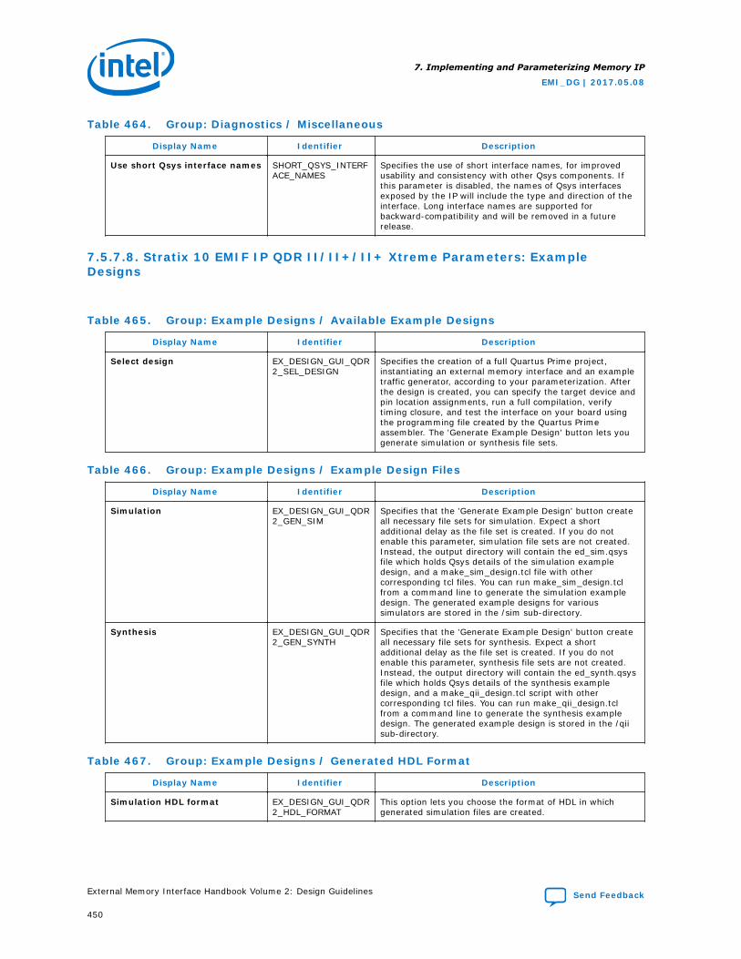
Table 464. Group: Diagnostics / Miscellaneous
Display Name Identifier Description
Use short Qsys interface names SHORT_QSYS_INTERFACE_NAMES
Specifies the use of short interface names, for improvedusability and consistency with other Qsys components. Ifthis parameter is disabled, the names of Qsys interfacesexposed by the IP will include the type and direction of theinterface. Long interface names are supported forbackward-compatibility and will be removed in a futurerelease.
7.5.7.8. Stratix 10 EMIF IP QDR II/II+/II+ Xtreme Parameters: ExampleDesigns
Table 465. Group: Example Designs / Available Example Designs
Display Name Identifier Description
Select design EX_DESIGN_GUI_QDR2_SEL_DESIGN
Specifies the creation of a full Quartus Prime project,instantiating an external memory interface and an exampletraffic generator, according to your parameterization. Afterthe design is created, you can specify the target device andpin location assignments, run a full compilation, verifytiming closure, and test the interface on your board usingthe programming file created by the Quartus Primeassembler. The 'Generate Example Design' button lets yougenerate simulation or synthesis file sets.
Table 466. Group: Example Designs / Example Design Files
Display Name Identifier Description
Simulation EX_DESIGN_GUI_QDR2_GEN_SIM
Specifies that the 'Generate Example Design' button createall necessary file sets for simulation. Expect a shortadditional delay as the file set is created. If you do notenable this parameter, simulation file sets are not created.Instead, the output directory will contain the ed_sim.qsysfile which holds Qsys details of the simulation exampledesign, and a make_sim_design.tcl file with othercorresponding tcl files. You can run make_sim_design.tclfrom a command line to generate the simulation exampledesign. The generated example designs for varioussimulators are stored in the /sim sub-directory.
Synthesis EX_DESIGN_GUI_QDR2_GEN_SYNTH
Specifies that the 'Generate Example Design' button createall necessary file sets for synthesis. Expect a shortadditional delay as the file set is created. If you do notenable this parameter, synthesis file sets are not created.Instead, the output directory will contain the ed_synth.qsysfile which holds Qsys details of the synthesis exampledesign, and a make_qii_design.tcl script with othercorresponding tcl files. You can run make_qii_design.tclfrom a command line to generate the synthesis exampledesign. The generated example design is stored in the /qiisub-directory.
Table 467. Group: Example Designs / Generated HDL Format
Display Name Identifier Description
Simulation HDL format EX_DESIGN_GUI_QDR2_HDL_FORMAT
This option lets you choose the format of HDL in whichgenerated simulation files are created.
7. Implementing and Parameterizing Memory IP
EMI_DG | 2017.05.08
External Memory Interface Handbook Volume 2: Design Guidelines Send Feedback
450

Table 468. Group: Example Designs / Target Development Kit
Display Name Identifier Description
Select board EX_DESIGN_GUI_QDR2_TARGET_DEV_KIT
Specifies that when you select a development kit with amemory module, the generated example design contains allsettings and fixed pin assignments to run on the selectedboard. You must select a development kit preset togenerate a working example design for the specifieddevelopment kit. Any IP settings not applied directly from adevelopment kit preset will not have guaranteed resultswhen testing the development kit. To exclude hardwaresupport of the example design, select 'none' from the'Select board' pull down menu. When you apply adevelopment kit preset, all IP parameters are automaticallyset appropriately to match the selected preset. If you wantto save your current settings, you should do so before youapply the preset. You can save your settings under adifferent name using File->Save as.
7.5.7.9. About Memory Presets
Presets help simplify the process of copying memory parameter values from memorydevice data sheets to the EMIF parameter editor.
For DDRx protocols, the memory presets are named using the following convention:
PROTOCOL-SPEEDBIN LATENCY FORMAT-AND-TOPOLOGY CAPACITY (INTERNAL-ORGANIZATION)
For example, the preset named DDR4-2666U CL18 Component 1CS 2Gb (512Mbx 4) refers to a DDR4 x4 component rated at the DDR4-2666U JEDEC speed bin, withnominal CAS latency of 18 cycles, one chip-select, and a total memory space of 2Gb.The JEDEC memory specification defines multiple speed bins for a given frequency(that is, DDR4-2666U and DDR4-2666V). You may be able to determine the exactspeed bin implemented by your memory device using its nominal latency. When indoubt, contact your memory vendor.
For RLDRAMx and QDRx protocols, the memory presets are named based on thevendor's device part number.
When the preset list does not contain the exact configuration required, you can stillminimize data entry by selecting the preset closest to your configuration and thenmodify parameters as required.
Prior to production you should always review the parameter values to ensure that theymatch your memory device data sheet, regardless of whether a preset is used or not.Incorrect memory parameters can cause functional failures.
7.5.8. Stratix 10 EMIF IP RLDRAM 3 Parameters
The Stratix 10 EMIF IP parameter editor allows you to parameterize settings for theStratix 10 EMIF IP.
The text window at the bottom of the parameter editor displays information about thememory interface, as well as warning and error messages. You should correct anyerrors indicated in this window before clicking the Finish button.
Note: Default settings are the minimum required to achieve timing, and may vary dependingon memory protocol.
7. Implementing and Parameterizing Memory IP
EMI_DG | 2017.05.08
Send Feedback External Memory Interface Handbook Volume 2: Design Guidelines
451

The following tables describe the parameterization settings available in the parametereditor for the Stratix 10 EMIF IP.
7.5.8.1. Stratix 10 EMIF IP RLDRAM 3 Parameters: General
Table 469. Group: General / FPGA
Display Name Identifier Description
Speed grade PHY_FPGA_SPEEDGRADE_GUI
Indicates the device speed grade, and whether it is anengineering sample (ES) or production device. This value isbased on the device that you select in the parameter editor.If you do not specify a device, the system assumes adefault value. Ensure that you always specify the correctdevice during IP generation, otherwise your IP may notwork in hardware.
Table 470. Group: General / Interface
Display Name Identifier Description
Configuration PHY_CONFIG_ENUM Specifies the configuration of the memory interface. Theavailable options depend on the protocol in use. Optionsinclude Hard PHY and Hard Controller, Hard PHY and SoftController, or Hard PHY only. If you select Hard PHY only,the AFI interface is exported to allow connection of acustom memory controller or third-party IP.
Instantiate two controllerssharing a Ping Pong PHY
PHY_PING_PONG_EN Specifies the instantiation of two identical memorycontrollers that share an address/command bus through theuse of Ping Pong PHY. This parameter is available only if youspecify the Hard PHY and Hard Controller option. When thisparameter is enabled, the IP exposes two independentAvalon interfaces to the user logic, and a single externalmemory interface with double width for the data bus andthe CS#, CKE, ODT, and CK/CK# signals.
Table 471. Group: General / Clocks
Display Name Identifier Description
Core clocks sharing PHY_CORE_CLKS_SHARING_ENUM
When a design contains multiple interfaces of the sameprotocol, rate, frequency, and PLL reference clock source,they can share a common set of core clock domains. Bysharing core clock domains, they reduce clock networkusage and avoid clock synchronization logic between theinterfaces. To share core clocks, denote one of theinterfaces as "Master", and the remaining interfaces as"Slave". In the RTL, connect the clks_sharing_master_outsignal from the master interface to theclks_sharing_slave_in signal of all the slave interfaces. Bothmaster and slave interfaces still expose their own outputclock ports in the RTL (for example, emif_usr_clk, afi_clk),but the physical signals are equivalent, hence it does notmatter whether a clock port from a master or a slave isused. As the combined width of all interfaces sharing thesame core clock increases, you may encounter timingclosure difficulty for transfers between the FPGA core andthe periphery.
Memory clock frequency PHY_MEM_CLK_FREQ_MHZ
Specifies the operating frequency of the memory interfacein MHz. If you change the memory frequency, you shouldupdate the memory latency parameters on the "Memory"tab and the memory timing parameters on the "MemTiming" tab.
continued...
7. Implementing and Parameterizing Memory IP
EMI_DG | 2017.05.08
External Memory Interface Handbook Volume 2: Design Guidelines Send Feedback
452

Display Name Identifier Description
Clock rate of user logic PHY_RATE_ENUM Specifies the relationship between the user logic clockfrequency and the memory clock frequency. For example, ifthe memory clock sent from the FPGA to the memorydevice is toggling at 800MHz, a quarter-rate interfacemeans that the user logic in the FPGA runs at 200MHz.
PLL reference clock frequency PHY_REF_CLK_FREQ_MHZ
Specifies the PLL reference clock frequency. You mustconfigure this parameter only if you do not check the "Userecommended PLL reference clock frequency" parameter. Toconfigure this parameter, select a valid PLL reference clockfrequency from the list. The values in the list can change ifyou change the memory interface frequency and/or theclock rate of the user logic. For best jitter performance, youshould use the fastest possible PLL reference clockfrequency.
PLL reference clock jitter PHY_REF_CLK_JITTER_PS
Specifies the peak-to-peak jitter on the PLL reference clocksource. The clock source of the PLL reference clock mustmeet or exceed the following jitter requirements: 10ps peakto peak, or 1.42ps RMS at 1e-12 BER, 1.22ps at 1e-16 BER.
Use recommended PLLreference clock frequency
PHY_RLD3_DEFAULT_REF_CLK_FREQ
Specifies that the PLL reference clock frequency isautomatically calculated for best performance. If you wantto specify a different PLL reference clock frequency, uncheckthe check box for this parameter.
Specify additional core clocksbased on existing PLL
PLL_ADD_EXTRA_CLKS
Displays additional parameters allowing you to createadditional output clocks based on the existing PLL. Thisparameter provides an alternative clock-generationmechanism for when your design exhausts available PLLresources. The additional output clocks that you create canbe fed into the core. Clock signals created with thisparameter are synchronous to each other, but asynchronousto the memory interface core clock domains (such asemif_usr_clk or afi_clk). You must follow proper clock-domain-crossing techniques when transferring data betweenclock domains.
Table 472. Group: General / Additional Core Clocks
Display Name Identifier Description
Number of additional coreclocks
PLL_USER_NUM_OF_EXTRA_CLKS
Specifies the number of additional output clocks to createfrom the PLL.
7.5.8.2. Stratix 10 EMIF IP RLDRAM 3 Parameters: Memory
Table 473. Group: Memory / Topology
Display Name Identifier Description
Address width MEM_RLD3_ADDR_WIDTH
Number of address pins.
CS# width MEM_RLD3_CS_WIDTH
Number of chip selects of the memory interface.
Enable depth expansion usingtwin die package
MEM_RLD3_DEPTH_EXPANDED
Indicates whether to combine two RLDRAM3 devices todouble the address space, resulting in more density.
DK width MEM_RLD3_DK_WIDTH
Number of DK clock pairs of the memory interface. This isequal to the number of write data groups, and isautomatically calculated based on the DQ width per deviceand whether width expansion is enabled.
continued...
7. Implementing and Parameterizing Memory IP
EMI_DG | 2017.05.08
Send Feedback External Memory Interface Handbook Volume 2: Design Guidelines
453
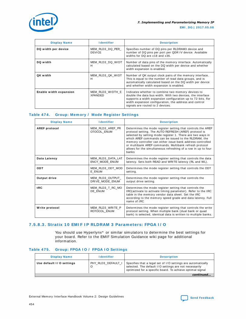
Display Name Identifier Description
DQ width per device MEM_RLD3_DQ_PER_DEVICE
Specifies number of DQ pins per RLDRAM3 device andnumber of DQ pins per port per QDR IV device. Availablewidths for DQ are x18 and x36.
DQ width MEM_RLD3_DQ_WIDTH
Number of data pins of the memory interface. Automaticallycalculated based on the DQ width per device and whetherwidth expansion is enabled.
QK width MEM_RLD3_QK_WIDTH
Number of QK output clock pairs of the memory interface.This is equal to the number of read data groups, and isautomatically calculated based on the DQ width per deviceand whether width expansion is enabled.
Enable width expansion MEM_RLD3_WIDTH_EXPANDED
Indicates whether to combine two memory devices todouble the data bus width. With two devices, the interfacesupports a width expansion configuration up to 72-bits. Forwidth expansion configuration, the address and controlsignals are routed to 2 devices.
Table 474. Group: Memory / Mode Register Settings
Display Name Identifier Description
AREF protocol MEM_RLD3_AREF_PROTOCOL_ENUM
Determines the mode register setting that controls the AREFprotocol setting. The AUTO REFRESH (AREF) protocol isselected by setting mode register 1. There are two ways inwhich AREF commands can be issued to the RLDRAM, thememory controller can either issue bank address-controlledor multibank AREF commands. Multibank refresh protocolallows for the simultaneous refreshing of a row in up to fourbanks
Data Latency MEM_RLD3_DATA_LATENCY_MODE_ENUM
Determines the mode register setting that controls the datalatency. Sets both READ and WRITE latency (RL and WL).
ODT MEM_RLD3_ODT_MODE_ENUM
Determines the mode register setting that controls the ODTsetting.
Output drive MEM_RLD3_OUTPUT_DRIVE_MODE_ENUM
Determines the mode register setting that controls theoutput drive setting.
tRC MEM_RLD3_T_RC_MODE_ENUM
Determines the mode register setting that controls thetRC(activate to activate timing parameter). Refer to the tRCtable in the memory vendor data sheet. Set the tRCaccording to the memory speed grade and data latency. Fullname of tRC
Write protocol MEM_RLD3_WRITE_PROTOCOL_ENUM
Determines the mode register setting that controls the writeprotocol setting. When multiple bank (dual bank or quadbank) is selected, identical data is written to multiple banks.
7.5.8.3. Stratix 10 EMIF IP RLDRAM 3 Parameters: FPGA I/O
You should use Hyperlynx* or similar simulators to determine the best settings foryour board. Refer to the EMIF Simulation Guidance wiki page for additionalinformation.
Table 475. Group: FPGA IO / FPGA IO Settings
Display Name Identifier Description
Use default I/O settings PHY_RLD3_DEFAULT_IO
Specifies that a legal set of I/O settings are automaticallyselected. The default I/O settings are not necessarilyoptimized for a specific board. To achieve optimal signal
continued...
7. Implementing and Parameterizing Memory IP
EMI_DG | 2017.05.08
External Memory Interface Handbook Volume 2: Design Guidelines Send Feedback
454
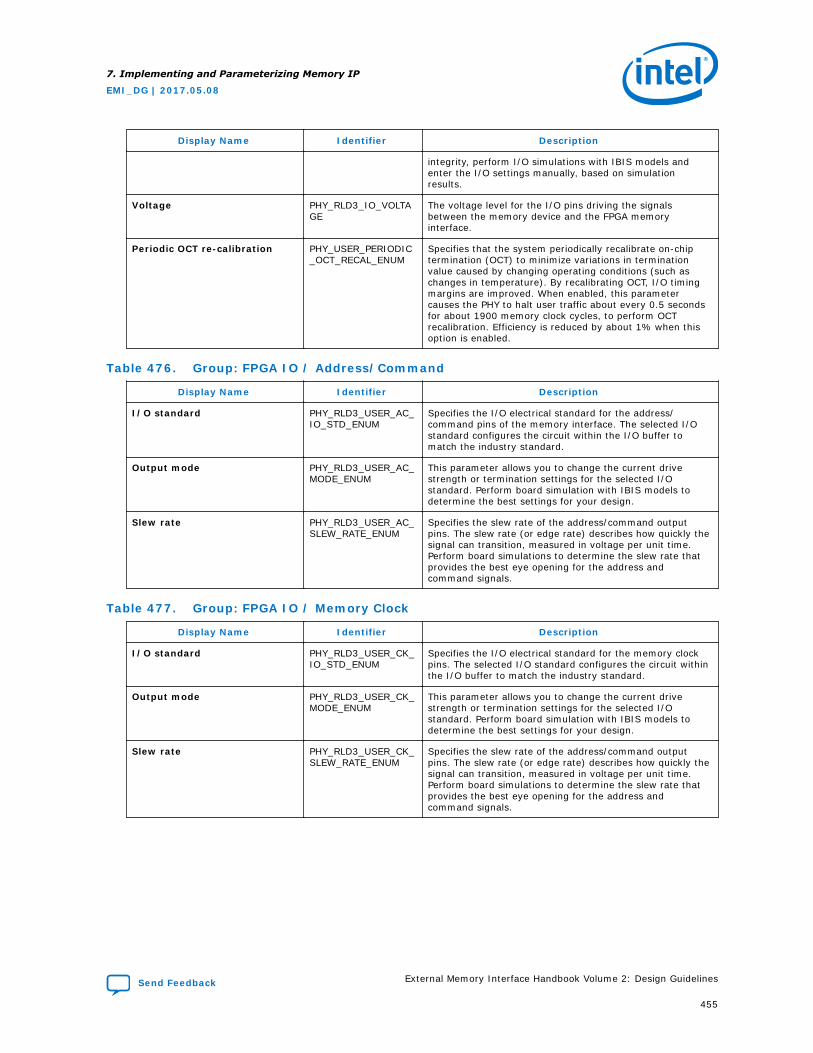
Display Name Identifier Description
integrity, perform I/O simulations with IBIS models andenter the I/O settings manually, based on simulationresults.
Voltage PHY_RLD3_IO_VOLTAGE
The voltage level for the I/O pins driving the signalsbetween the memory device and the FPGA memoryinterface.
Periodic OCT re-calibration PHY_USER_PERIODIC_OCT_RECAL_ENUM
Specifies that the system periodically recalibrate on-chiptermination (OCT) to minimize variations in terminationvalue caused by changing operating conditions (such aschanges in temperature). By recalibrating OCT, I/O timingmargins are improved. When enabled, this parametercauses the PHY to halt user traffic about every 0.5 secondsfor about 1900 memory clock cycles, to perform OCTrecalibration. Efficiency is reduced by about 1% when thisoption is enabled.
Table 476. Group: FPGA IO / Address/Command
Display Name Identifier Description
I/O standard PHY_RLD3_USER_AC_IO_STD_ENUM
Specifies the I/O electrical standard for the address/command pins of the memory interface. The selected I/Ostandard configures the circuit within the I/O buffer tomatch the industry standard.
Output mode PHY_RLD3_USER_AC_MODE_ENUM
This parameter allows you to change the current drivestrength or termination settings for the selected I/Ostandard. Perform board simulation with IBIS models todetermine the best settings for your design.
Slew rate PHY_RLD3_USER_AC_SLEW_RATE_ENUM
Specifies the slew rate of the address/command outputpins. The slew rate (or edge rate) describes how quickly thesignal can transition, measured in voltage per unit time.Perform board simulations to determine the slew rate thatprovides the best eye opening for the address andcommand signals.
Table 477. Group: FPGA IO / Memory Clock
Display Name Identifier Description
I/O standard PHY_RLD3_USER_CK_IO_STD_ENUM
Specifies the I/O electrical standard for the memory clockpins. The selected I/O standard configures the circuit withinthe I/O buffer to match the industry standard.
Output mode PHY_RLD3_USER_CK_MODE_ENUM
This parameter allows you to change the current drivestrength or termination settings for the selected I/Ostandard. Perform board simulation with IBIS models todetermine the best settings for your design.
Slew rate PHY_RLD3_USER_CK_SLEW_RATE_ENUM
Specifies the slew rate of the address/command outputpins. The slew rate (or edge rate) describes how quickly thesignal can transition, measured in voltage per unit time.Perform board simulations to determine the slew rate thatprovides the best eye opening for the address andcommand signals.
7. Implementing and Parameterizing Memory IP
EMI_DG | 2017.05.08
Send Feedback External Memory Interface Handbook Volume 2: Design Guidelines
455

Table 478. Group: FPGA IO / Data Bus
Display Name Identifier Description
Use recommended initial Vrefin PHY_RLD3_USER_AUTO_STARTING_VREFIN_EN
Specifies that the initial Vrefin setting is calculatedautomatically, to a reasonable value based on terminationsettings.
Input mode PHY_RLD3_USER_DATA_IN_MODE_ENUM
This parameter allows you to change the input terminationsettings for the selected I/O standard. Perform boardsimulation with IBIS models to determine the best settingsfor your design.
I/O standard PHY_RLD3_USER_DATA_IO_STD_ENUM
Specifies the I/O electrical standard for the data and dataclock/strobe pins of the memory interface. The selected I/Ostandard option configures the circuit within the I/O bufferto match the industry standard.
Output mode PHY_RLD3_USER_DATA_OUT_MODE_ENUM
This parameter allows you to change the output currentdrive strength or termination settings for the selected I/Ostandard. Perform board simulation with IBIS models todetermine the best settings for your design.
Initial Vrefin PHY_RLD3_USER_STARTING_VREFIN
Specifies the initial value for the reference voltage on thedata pins (Vrefin). This value is entered as a percentage ofthe supply voltage level on the I/O pins. The specified valueserves as a starting point and may be overridden bycalibration to provide better timing margins. If you chooseto skip Vref calibration (Diagnostics tab), this is the valuethat is used as the Vref for the interface.
Table 479. Group: FPGA IO / PHY Inputs
Display Name Identifier Description
PLL reference clock I/Ostandard
PHY_RLD3_USER_PLL_REF_CLK_IO_STD_ENUM
Specifies the I/O standard for the PLL reference clock of thememory interface.
RZQ I/O standard PHY_RLD3_USER_RZQ_IO_STD_ENUM
Specifies the I/O standard for the RZQ pin used in thememory interface.
RZQ resistor PHY_RZQ Specifies the reference resistor used to calibrate the on-chiptermination value. You should connect the RZQ pin to GNDthrough an external resistor of the specified value.
7.5.8.4. Stratix 10 EMIF IP RLDRAM 3 Parameters: Mem Timing
These parameters should be read from the table in the datasheet associated with thespeed bin of the memory device (not necessarily the frequency at which the interfaceis running).
Table 480. Group: Mem Timing / Parameters dependent on Speed Bin
Display Name Identifier Description
Speed bin MEM_RLD3_SPEEDBIN_ENUM
The speed grade of the memory device used. Thisparameter refers to the maximum rate at which thememory device is specified to run.
tCKDK_max MEM_RLD3_TCKDK_MAX_CYC
tCKDK_max refers to the maximum skew from the memoryclock (CK) to the write strobe (DK).
tCKDK_min MEM_RLD3_TCKDK_MIN_CYC
tCKDK_min refers to the minimum skew from the memoryclock (CK) to the write strobe (DK).
tCKQK_max MEM_RLD3_TCKQK_MAX_PS
tCKQK_max refers to the maximum skew from the memoryclock (CK) to the read strobe (QK).
continued...
7. Implementing and Parameterizing Memory IP
EMI_DG | 2017.05.08
External Memory Interface Handbook Volume 2: Design Guidelines Send Feedback
456

Display Name Identifier Description
tDH (base) DC level MEM_RLD3_TDH_DC_MV
tDH (base) DC level refers to the voltage level which thedata bus must not cross during the hold window. The signalis considered stable only if it remains above this voltagelevel (for a logic 1) or below this voltage level (for a logic 0)for the entire hold period.
tDH (base) MEM_RLD3_TDH_PS tDH (base) refers to the hold time for the Data (DQ) busafter the rising edge of CK.
tDS (base) AC level MEM_RLD3_TDS_AC_MV
tDS (base) AC level refers to the voltage level which thedata bus must cross and remain above during the setupmargin window. The signal is considered stable only if itremains above this voltage level (for a logic 1) or below thisvoltage level (for a logic 0) for the entire setup period.
tDS (base) MEM_RLD3_TDS_PS tDS(base) refers to the setup time for the Data (DQ) busbefore the rising edge of the DQS strobe.
tIH (base) DC level MEM_RLD3_TIH_DC_MV
tIH (base) DC level refers to the voltage level which theaddress/command signal must not cross during the holdwindow. The signal is considered stable only if it remainsabove this voltage level (for a logic 1) or below this voltagelevel (for a logic 0) for the entire hold period.
tIH (base) MEM_RLD3_TIH_PS tIH (base) refers to the hold time for the Address/Command(A) bus after the rising edge of CK. Depending on what AClevel the user has chosen for a design, the hold margin canvary (this variance will be automatically determined whenthe user choses the "tIH (base) AC level").
tIS (base) AC level MEM_RLD3_TIS_AC_MV
tIS (base) AC level refers to the voltage level which theaddress/command signal must cross and remain aboveduring the setup margin window. The signal is consideredstable only if it remains above this voltage level (for a logic1) or below this voltage level (for a logic 0) for the entiresetup period.
tIS (base) MEM_RLD3_TIS_PS tIS (base) refers to the setup time for the Address/Command/Control (A) bus to the rising edge of CK.
tQH MEM_RLD3_TQH_CYC tQH specifies the output hold time for the DQ/DINV inrelation to QK.
tQKQ_max MEM_RLD3_TQKQ_MAX_PS
tQKQ_max describes the maximum skew between the readstrobe (QK) clock edge to the data bus (DQ/DINV) edge.
7.5.8.5. Stratix 10 EMIF IP RLDRAM 3 Parameters: Board
Table 481. Group: Board / Intersymbol Interference/Crosstalk
Display Name Identifier Description
Address and command ISI/crosstalk
BOARD_RLD3_USER_AC_ISI_NS
The address and command window reduction due to ISI andcrosstalk effects. The number to be entered is the total lossof margin on both the setup and hold sides (measured losson the setup side + measured loss on the hold side). Referto the EMIF Simulation Guidance wiki page for additionalinformation.
QK/QK# ISI/crosstalk BOARD_RLD3_USER_RCLK_ISI_NS
QK/QK# ISI/crosstalk describes the reduction of the readdata window due to intersymbol interference and crosstalkeffects on the QK/QK# signal when driven by the memorydevice during a read. The number to be entered in theQuartus Prime software is the total of the measured loss of
continued...
7. Implementing and Parameterizing Memory IP
EMI_DG | 2017.05.08
Send Feedback External Memory Interface Handbook Volume 2: Design Guidelines
457
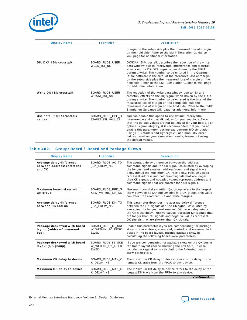
Display Name Identifier Description
margin on the setup side plus the measured loss of marginon the hold side. Refer to the EMIF Simulation Guidancewiki page for additional information.
DK/DK# ISI/crosstalk BOARD_RLD3_USER_WCLK_ISI_NS
DK/DK# ISI/crosstalk describes the reduction of the writedata window due to intersymbol interference and crosstalkeffects on the DK/DK# signal when driven by the FPGAduring a write. The number to be entered in the QuartusPrime software is the total of the measured loss of marginon the setup side plus the measured loss of margin on thehold side. Refer to the EMIF Simulation Guidance wiki pagefor additional information.
Write DQ ISI/crosstalk BOARD_RLD3_USER_WDATA_ISI_NS
The reduction of the write data window due to ISI andcrosstalk effects on the DQ signal when driven by the FPGAduring a write. The number to be entered is the total of themeasured loss of margin on the setup side plus themeasured loss of margin on the hold side. Refer to the EMIFSimulation Guidance wiki page for additional information.
Use default ISI/crosstalkvalues
BOARD_RLD3_USE_DEFAULT_ISI_VALUES
You can enable this option to use default intersymbolinterference and crosstalk values for your topology. Notethat the default values are not optimized for your board. Foroptimal signal integrity, it is recommended that you do notenable this parameter, but instead perform I/O simulationusing IBIS models and Hyperlynx*, and manually entervalues based on your simulation results, instead of usingthe default values.
Table 482. Group: Board / Board and Package Skews
Display Name Identifier Description
Average delay differencebetween address/commandand CK
BOARD_RLD3_AC_TO_CK_SKEW_NS
The average delay difference between the address/command signals and the CK signal, calculated by averagingthe longest and smallest address/command signal tracedelay minus the maximum CK trace delay. Positive valuesrepresent address and command signals that are longerthan CK signals and negative values represent address andcommand signals that are shorter than CK signals.
Maximum board skew withinQK group
BOARD_RLD3_BRD_SKEW_WITHIN_QK_NS
Maximum board skew within QK group refers to the largestskew between all DQ and DM pins in a QK group. This valuecan affect the read capture and write margins.
Average delay differencebetween DK and CK
BOARD_RLD3_DK_TO_CK_SKEW_NS
This parameter describes the average delay differencebetween the DK signals and the CK signal, calculated byaveraging the longest and smallest DK trace delay minusthe CK trace delay. Positive values represent DK signals thatare longer than CK signals and negative values representDK signals that are shorter than CK signals.
Package deskewed with boardlayout (address/commandbus)
BOARD_RLD3_IS_SKEW_WITHIN_AC_DESKEWED
Enable this parameter if you are compensating for packageskew on the address, command, control, and memory clockbuses in the board layout. Include package skew incalculating the following board skew parameters.
Package deskewed with boardlayout (QK group)
BOARD_RLD3_IS_SKEW_WITHIN_QK_DESKEWED
If you are compensating for package skew on the QK bus inthe board layout (hence checking the box here), pleaseinclude package skew in calculating the following boardskew parameters.
Maximum CK delay to device BOARD_RLD3_MAX_CK_DELAY_NS
The maximum CK delay to device refers to the delay of thelongest CK trace from the FPGA to any device.
Maximum DK delay to device BOARD_RLD3_MAX_DK_DELAY_NS
The maximum DK delay to device refers to the delay of thelongest DK trace from the FPGA to any device.
continued...
7. Implementing and Parameterizing Memory IP
EMI_DG | 2017.05.08
External Memory Interface Handbook Volume 2: Design Guidelines Send Feedback
458

Display Name Identifier Description
Maximum system skew withinaddress/command bus
BOARD_RLD3_PKG_BRD_SKEW_WITHIN_AC_NS
Maximum system skew within address/command bus refersto the largest skew between the address and commandsignals.
Maximum delay differencebetween devices
BOARD_RLD3_SKEW_BETWEEN_DIMMS_NS
This parameter describes the largest propagation delay onthe DQ signals between ranks. For example, in a two-rankconfiguration where devices are placed in series, there is anextra propagation delay for DQ signals going to and comingback from the furthest device compared to the nearestdevice. This parameter is only applicable when there ismore than one rank.
Maximum skew between DKgroups
BOARD_RLD3_SKEW_BETWEEN_DK_NS
This parameter describes the largest skew between DKsignals in different DK groups.
7.5.8.6. Stratix 10 EMIF IP RLDRAM 3 Parameters: Diagnostics
Table 483. Group: Diagnostics / Simulation Options
Display Name Identifier Description
Abstract phy for fast simulation DIAG_RLD3_ABSTRACT_PHY
Specifies that the system use Abstract PHY for simulation.Abstract PHY replaces the PHY with a model for fastsimulation and can reduce simulation time by 2-3 times.Abstract PHY is available for certain protocols and devicefamilies, and only when you select Skip Calibration.
Calibration mode DIAG_SIM_CAL_MODE_ENUM
Specifies whether to skip memory interface calibrationduring simulation, or to simulate the full calibration process.Simulating the full calibration process can take hours (oreven days), depending on the width and depth of thememory interface. You can achieve much faster simulationtimes by skipping the calibration process, but that is onlyexpected to work when the memory model is ideal and theinterconnect delays are zero. If you enable this parameter,the interface still performs some memory initializationbefore starting normal operations. Abstract PHY issupported with skip calibration.
Table 484. Group: Diagnostics / Calibration Debug Options
Display Name Identifier Description
Enable Daisy-Chaining forQuartus Prime EMIF DebugToolkit/On-Chip Debug Port
DIAG_EXPORT_SEQ_AVALON_MASTER
Specifies that the IP export an Avalon-MM master interface(cal_debug_out) which can connect to the cal_debuginterface of other EMIF cores residing in the same I/Ocolumn. This parameter applies only if the EMIF DebugToolkit or On-Chip Debug Port is enabled. Refer to theDebugging Multiple EMIFs wiki page for more informationabout debugging multiple EMIFs.
Quartus Prime EMIF DebugToolkit/On-Chip Debug Port
DIAG_EXPORT_SEQ_AVALON_SLAVE
Specifies the connectivity of an Avalon slave interface foruse by the Quartus Prime EMIF Debug Toolkit or user corelogic. If you set this parameter to "Disabled," no debugfeatures are enabled. If you set this parameter to "Export,"an Avalon slave interface named "cal_debug" is exportedfrom the IP. To use this interface with the EMIF DebugToolkit, you must instantiate and connect an EMIF debuginterface IP core to it, or connect it to the cal_debug_outinterface of another EMIF core. If you select "Add EMIFDebug Interface", an EMIF debug interface componentcontaining a JTAG Avalon Master is connected to the debugport, allowing the core to be accessed by the EMIF Debug
continued...
7. Implementing and Parameterizing Memory IP
EMI_DG | 2017.05.08
Send Feedback External Memory Interface Handbook Volume 2: Design Guidelines
459
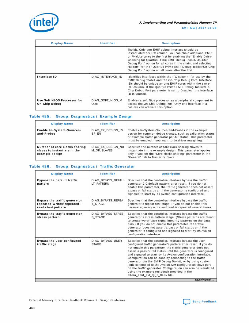
Display Name Identifier Description
Toolkit. Only one EMIF debug interface should beinstantiated per I/O column. You can chain additional EMIFor PHYLite cores to the first by enabling the "Enable Daisy-Chaining for Quartus Prime EMIF Debug Toolkit/On-ChipDebug Port" option for all cores in the chain, and selecting"Export" for the "Quartus Prime EMIF Debug Toolkit/On-ChipDebug Port" option on all cores after the first.
Interface ID DIAG_INTERFACE_ID Identifies interfaces within the I/O column, for use by theEMIF Debug Toolkit and the On-Chip Debug Port. InterfaceIDs should be unique among EMIF cores within the sameI/O column. If the Quartus Prime EMIF Debug Toolkit/On-Chip Debug Port parameter is set to Disabled, the interfaceID is unused.
Use Soft NIOS Processor forOn-Chip Debug
DIAG_SOFT_NIOS_MODE
Enables a soft Nios processor as a peripheral component toaccess the On-Chip Debug Port. Only one interface in acolumn can activate this option.
Table 485. Group: Diagnostics / Example Design
Display Name Identifier Description
Enable In-System-Sources-and-Probes
DIAG_EX_DESIGN_ISSP_EN
Enables In-System-Sources-and-Probes in the exampledesign for common debug signals, such as calibration statusor example traffic generator per-bit status. This parametermust be enabled if you want to do driver margining.
Number of core clocks sharingslaves to instantiate in theexample design
DIAG_EX_DESIGN_NUM_OF_SLAVES
Specifies the number of core clock sharing slaves toinstantiate in the example design. This parameter appliesonly if you set the "Core clocks sharing" parameter in the"General" tab to Master or Slave.
Table 486. Group: Diagnostics / Traffic Generator
Display Name Identifier Description
Bypass the default trafficpattern
DIAG_BYPASS_DEFAULT_PATTERN
Specifies that the controller/interface bypass the trafficgenerator 2.0 default pattern after reset. If you do notenable this parameter, the traffic generator does not asserta pass or fail status until the generator is configured andsignaled to start by its Avalon configuration interface.
Bypass the traffic generatorrepeated-writes/repeated-reads test pattern
DIAG_BYPASS_REPEAT_STAGE
Specifies that the controller/interface bypass the trafficgenerator's repeat test stage. If you do not enable thisparameter, every write and read is repeated several times.
Bypass the traffic generatorstress pattern
DIAG_BYPASS_STRESS_STAGE
Specifies that the controller/interface bypass the trafficgenerator's stress pattern stage. (Stress patterns are meantto create worst-case signal integrity patterns on the datapins.) If you do not enable this parameter, the trafficgenerator does not assert a pass or fail status until thegenerator is configured and signaled to start by its Avalonconfiguration interface.
Bypass the user-configuredtraffic stage
DIAG_BYPASS_USER_STAGE
Specifies that the controller/interface bypass the user-configured traffic generator's pattern after reset. If you donot enable this parameter, the traffic generator does notassert a pass or fail status until the generator is configuredand signaled to start by its Avalon configuration interface.Configuration can be done by connecting to the trafficgenerator via the EMIF Debug Toolkit, or by using customlogic connected to the Avalon-MM configuration slave porton the traffic generator. Configuration can also be simulatedusing the example testbench provided in thealtera_emif_avl_tg_2_tb.sv file.
continued...
7. Implementing and Parameterizing Memory IP
EMI_DG | 2017.05.08
External Memory Interface Handbook Volume 2: Design Guidelines Send Feedback
460
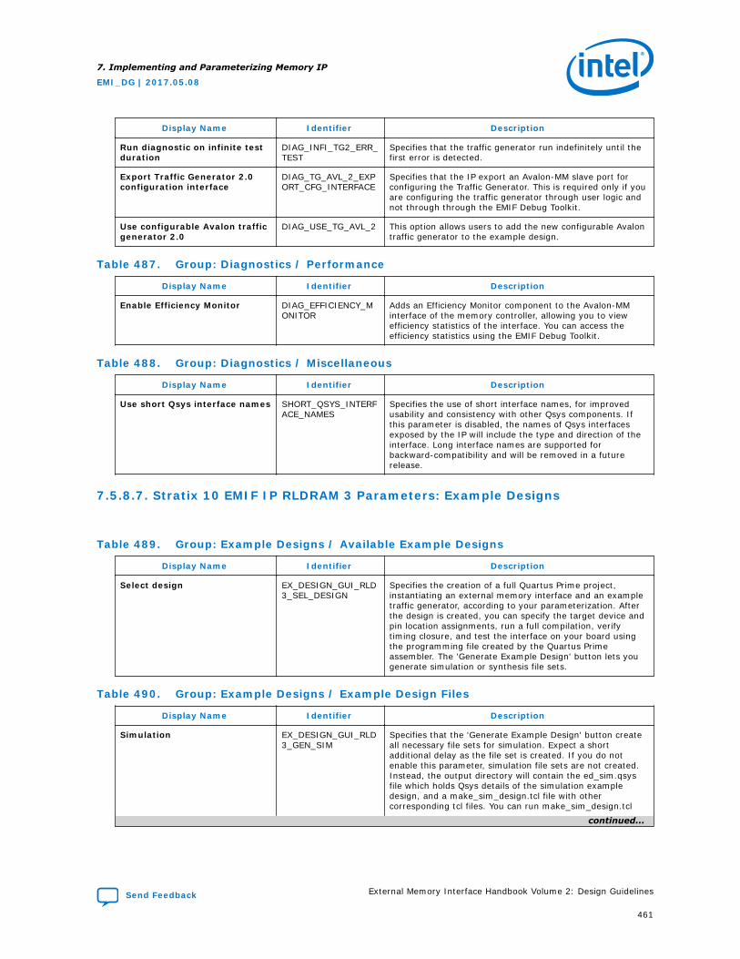
Display Name Identifier Description
Run diagnostic on infinite testduration
DIAG_INFI_TG2_ERR_TEST
Specifies that the traffic generator run indefinitely until thefirst error is detected.
Export Traffic Generator 2.0configuration interface
DIAG_TG_AVL_2_EXPORT_CFG_INTERFACE
Specifies that the IP export an Avalon-MM slave port forconfiguring the Traffic Generator. This is required only if youare configuring the traffic generator through user logic andnot through through the EMIF Debug Toolkit.
Use configurable Avalon trafficgenerator 2.0
DIAG_USE_TG_AVL_2 This option allows users to add the new configurable Avalontraffic generator to the example design.
Table 487. Group: Diagnostics / Performance
Display Name Identifier Description
Enable Efficiency Monitor DIAG_EFFICIENCY_MONITOR
Adds an Efficiency Monitor component to the Avalon-MMinterface of the memory controller, allowing you to viewefficiency statistics of the interface. You can access theefficiency statistics using the EMIF Debug Toolkit.
Table 488. Group: Diagnostics / Miscellaneous
Display Name Identifier Description
Use short Qsys interface names SHORT_QSYS_INTERFACE_NAMES
Specifies the use of short interface names, for improvedusability and consistency with other Qsys components. Ifthis parameter is disabled, the names of Qsys interfacesexposed by the IP will include the type and direction of theinterface. Long interface names are supported forbackward-compatibility and will be removed in a futurerelease.
7.5.8.7. Stratix 10 EMIF IP RLDRAM 3 Parameters: Example Designs
Table 489. Group: Example Designs / Available Example Designs
Display Name Identifier Description
Select design EX_DESIGN_GUI_RLD3_SEL_DESIGN
Specifies the creation of a full Quartus Prime project,instantiating an external memory interface and an exampletraffic generator, according to your parameterization. Afterthe design is created, you can specify the target device andpin location assignments, run a full compilation, verifytiming closure, and test the interface on your board usingthe programming file created by the Quartus Primeassembler. The 'Generate Example Design' button lets yougenerate simulation or synthesis file sets.
Table 490. Group: Example Designs / Example Design Files
Display Name Identifier Description
Simulation EX_DESIGN_GUI_RLD3_GEN_SIM
Specifies that the 'Generate Example Design' button createall necessary file sets for simulation. Expect a shortadditional delay as the file set is created. If you do notenable this parameter, simulation file sets are not created.Instead, the output directory will contain the ed_sim.qsysfile which holds Qsys details of the simulation exampledesign, and a make_sim_design.tcl file with othercorresponding tcl files. You can run make_sim_design.tcl
continued...
7. Implementing and Parameterizing Memory IP
EMI_DG | 2017.05.08
Send Feedback External Memory Interface Handbook Volume 2: Design Guidelines
461

Display Name Identifier Description
from a command line to generate the simulation exampledesign. The generated example designs for varioussimulators are stored in the /sim sub-directory.
Synthesis EX_DESIGN_GUI_RLD3_GEN_SYNTH
Specifies that the 'Generate Example Design' button createall necessary file sets for synthesis. Expect a shortadditional delay as the file set is created. If you do notenable this parameter, synthesis file sets are not created.Instead, the output directory will contain the ed_synth.qsysfile which holds Qsys details of the synthesis exampledesign, and a make_qii_design.tcl script with othercorresponding tcl files. You can run make_qii_design.tclfrom a command line to generate the synthesis exampledesign. The generated example design is stored in the /qiisub-directory.
Table 491. Group: Example Designs / Generated HDL Format
Display Name Identifier Description
Simulation HDL format EX_DESIGN_GUI_RLD3_HDL_FORMAT
This option lets you choose the format of HDL in whichgenerated simulation files are created.
Table 492. Group: Example Designs / Target Development Kit
Display Name Identifier Description
Select board EX_DESIGN_GUI_RLD3_TARGET_DEV_KIT
Specifies that when you select a development kit with amemory module, the generated example design contains allsettings and fixed pin assignments to run on the selectedboard. You must select a development kit preset togenerate a working example design for the specifieddevelopment kit. Any IP settings not applied directly from adevelopment kit preset will not have guaranteed resultswhen testing the development kit. To exclude hardwaresupport of the example design, select 'none' from the'Select board' pull down menu. When you apply adevelopment kit preset, all IP parameters are automaticallyset appropriately to match the selected preset. If you wantto save your current settings, you should do so before youapply the preset. You can save your settings under adifferent name using File->Save as.
7.5.8.8. About Memory Presets
Presets help simplify the process of copying memory parameter values from memorydevice data sheets to the EMIF parameter editor.
For DDRx protocols, the memory presets are named using the following convention:
PROTOCOL-SPEEDBIN LATENCY FORMAT-AND-TOPOLOGY CAPACITY (INTERNAL-ORGANIZATION)
For example, the preset named DDR4-2666U CL18 Component 1CS 2Gb (512Mbx 4) refers to a DDR4 x4 component rated at the DDR4-2666U JEDEC speed bin, withnominal CAS latency of 18 cycles, one chip-select, and a total memory space of 2Gb.The JEDEC memory specification defines multiple speed bins for a given frequency(that is, DDR4-2666U and DDR4-2666V). You may be able to determine the exactspeed bin implemented by your memory device using its nominal latency. When indoubt, contact your memory vendor.
For RLDRAMx and QDRx protocols, the memory presets are named based on thevendor's device part number.
7. Implementing and Parameterizing Memory IP
EMI_DG | 2017.05.08
External Memory Interface Handbook Volume 2: Design Guidelines Send Feedback
462
When the preset list does not contain the exact configuration required, you can stillminimize data entry by selecting the preset closest to your configuration and thenmodify parameters as required.
Prior to production you should always review the parameter values to ensure that theymatch your memory device data sheet, regardless of whether a preset is used or not.Incorrect memory parameters can cause functional failures.
7.6. Document Revision History
Date Version Changes
May 2017 2017.05.08 • Added Stratix 10 External Memory Interface IP section.• Rebranded as Intel.
October 2016 2016.10.31 • Updated Generated Directory Structure and Key Files for ExampleSimulation Designs and Generated Directory Structure and Key Files forExample Synthesis Designs tables.
• Removed Parameterizing Arria 10 External Memory Interface IP section.• Added protocol-specific parameter sections for Arria 10 EMIF IP.• Added Equations for Arria 10 EMIF IP Board Skew Parameters section.
May 2016 2016.05.02 • Modified window duration in descriptions of tDQSCK Delta Medium andtDQSCK Delta Long in the Parameter Descriptions table in Memory TimingParameters for DDR2, DDR3, and LPDDR2 SDRAM for UniPHY IP.
• Modified description of Enable the Efficiency Monitor and Protocol Checkeron the Controller Avalon Interface in the Simulation Options table inDiagnostics for UniPHY IP.
• Removed cal_debug_burstcount from Interface: cal_debug_avalon_slavetable in Qsys Interfaces.
• Modified Direction information for entries in Interface:cal_debug_out_avalon_master table in Qsys Interfaces.
• Removed two rows from the Generated Directory Structure and Key Filesfor Simulation table in Generated Files for Arria 10 External MemoryInterface IP.
• Replaced Generated Directory Structure and Key Files for ExampleDesigns table with Generated Directory Structure and Key Files forExample Simulation Designs and Generated Directory Structure and KeyFiles for Example Synthesis Designs tables in Generated Files for Arria 10External Memory Interface IP.
• Added entry for Slew rate to Group: I/O / Address/Command and Group:I/O / Memory Clock tables in I/O Parameters for Arria 10 EMIF IP.
• Modified description of DDR3 LRDIMM additional control words entry inGroup: Memory Topology / Mode Register Settings table in MemoryTopology Parameters for Arria 10 EMIF IP.
• Modified supported protocol information for Enable Error Detection andCorrection Logic and Enable Auto Error Correction entries in Group:Controller / Configuration, Status and Error Handling table in ControllerParameters for Arria 10 EMIF IP.
• Minor change to description of Calibration mode in Group: Diagnostic /Simulation Options table in Diagnostic Parameters for Arria 10 EMIF IP.
• Added QDR-IV to supported protocols for Skip VREF calibration in Group:Diagnostic / Calibration Debug Options table in Diagnostic Parameters forArria 10 EMIF IP.
• Added Calibration address 0, Calibration address 1, and Enable automaticcalibration after reset to Group: Diagnostic / Calibration Debug Optionstable in Diagnostic Parameters for Arria 10 EMIF IP.
• Added Group: Diagnostic / Traffic Generator table to DiagnosticParameters for Arria 10 EMIF IP. Moved some entries from Group:Diagnostic / Example Design table to new Group: Diagnostic / TrafficGenerator table.
continued...
7. Implementing and Parameterizing Memory IP
EMI_DG | 2017.05.08
Send Feedback External Memory Interface Handbook Volume 2: Design Guidelines
463
Date Version Changes
November 2015 2015.11.02 • Added note to descriptions of Minimum delay difference between CK andDQS and Maximum delay difference between CK and DQS in Board Skewparameters for LPDDR2/DDR2/DDR3 SDRAM.
• Added text to description of Maximum skew between DQS groups in BoardSkew parameters for LPDDR2/DDR2/DDR3 SDRAM.
• Changed description of emif_usr_clk in the Interface:emif_usr_clk_clock_source table in Qsys Interfaces.
• Changed description of emif_usr_reset_n in the Interface:emif_usr_reset_reset_source table in Qsys Interfaces.
• Added Interface: emif_usr_clk_sec_clock_source and Interface:emif_usr_reset_sec_reset_source tables in Qsys Interfaces.
• Added several options to the Simulation Options, Calibration DebugOptions, and Example Design tables in Diagnostic Parameters for Arria 10EMIF IP.
• Changed instances of Quartus II to Quartus Prime.• Added LPDDR3• Removed Use address parity bit parameter for QDR IV• Removed following DDR4 parameters:
— Write CRC enable— DDR4 geardown mode— Per-DRAM addressability— Temperature sensor readout— Write CMD latency for CRC/DM enable— MPR read format— CS to Addr/CMD Latency— Enable DM pins— Addr/CMD persistent error— Write DBI— Read DBI
• Removed group board timing/slew rates table• Removed Maximum system skew within QK group parameters for
RLDRAM 3• Removed Maximum system skew within Q group and Maximum
skew within D group parameters
May 2015 2015.05.04 Added information to the Description column for thecal_debug_avalon_slave, cal_debug_clk_clock_sink, andcal_debug_out_reset_reset_source tables in the Qsys Interfaces topic.
December 2014 2014.12.15 • Added MAX 10 device support to the PHY Parameters table in PHY Settingsfor UniPHY IP
• Changed Memory Parameters for LPDDR2, DDR2, and DDR3 SDRAM tableto accommodate MAX 10 devices.
• Added Enable Deep Power-Down Controls parameter to Controller Settingstable in Controller Settings for UniPHY IP section.
• Arria 10 External Memory Interface IP section:— Removed references to Arria 10 devices from Board Settings topic in
UniPHY-Based External Memory Interface IP section. Added new BoardTiming topic.
— Added QDR IV support to tables in Qsys Interfaces section.— Removed afi_c from afi_conduit_end table and mem_c from
mem_conduit_end table.— Changed description of global_reset_n signal in the Interface:
global_reset_reset_sink table.— Added Board Timing section and subtopics.
• Changed Memory Initialization Options for DDR3 table to accommodateMAX 10 devices.
continued...
7. Implementing and Parameterizing Memory IP
EMI_DG | 2017.05.08
External Memory Interface Handbook Volume 2: Design Guidelines Send Feedback
464
Date Version Changes
• Replaced Parameter Descriptions table in Memory Timing Parameters forDDR2, DDR3, and LPDDR2 SDRAM for UniPHY IP section with new tableincluding LPDDR2.
• Removed General Settings for Arria 10 EMIF IP section.• Parameterizing Arria 10 External Memory Interface IP section:
— Added DDR4 support to tables.— Changed descriptions of RDIMM/LRDIMM control words and LRDIMM
additional control words in Group: Memory Topology / Mode RegisterSettings table.
— Removed Chip ID Width from Group: Memory Topology / Topologytable.
— Added entry for Instantiate two controllers sharing a Ping PongPHY, and expanded description of Configuration, in the Group:General / Interface table.
— Changed Total interface width entry to DQ width and changedPlace ALERT# pin to ALERT# pin placement in Group: MemoryTopology / Topology table.
August 2014 2014.08.15 • Added notes about Arria 10 EMIF IP to beginning of chapter.• Added IP Catalog to Design Flows figure.• Replaced MegaWizard Plug-In Manager Flow with IP Catalog Design Flow.• Revised Specify Parameters for the Qsys Flow and Completing the Qsys
System sections.• Added information to description of mem_doff_n in QDR II and QDR II+
SRAM Controller with UniPHY Interfaces table.• Reorganized into separate sections for UniPHY-Based External Memory
Interfaces and Arria 10 External Memory Interface IP.• Replaced the following sections with the new Arria 10 EMIF IP Interfaces
section:— DDR3 Controller with Arria 10 EMIF Interfaces— LPDDR2 SDRAM Controller with Arria 10 EMIF Interfaces— QDR II/II+ Controller with Arria 10 EMIF Interfaces— RLDRAM II Controller with Arria 10 EMIF Interfaces— RLDRAM 3 Controller with Arria 10 EMIF Interfaces
• Changed name of Generated Files for Memory Controllers with Arria 10EMIF IP section to Generated Files for Arria 10 External Memory InterfaceIP, and revised content.
• Revised content of General Settings for Arria 10 EMIF IP section.• Added Parameterizing Arria 10 External Memory Interface IP section.• Revised content of Memory Topology for LPDDR2, DDR3 and DDR4 SDRAM
for Arria 10 EMIF IP section.• Added Memory Parameters for QDR IV for Arria 10 EMIF IP section.• Revised Memory Parameters for RLDRAM 3 for Arria 10 EMIF IP section.• Added slew rate information for QDR II, QDR II+, and QDR II+ Xtreme to
table in Slew Rates for Arria 10 EMIF IP section.• Revised ISI Parameters table in Intersymbol Interference Channel Signal
Integrity for UniPHY IP section.• Revised description of fly-by topology for UDIMMs in Board Skews for
UniPHY IP section.• Added MAX 10 to Simulation Options table in Diagnostics for UniPHY IP
section.• Added note to descriptions of Minimum delay difference between
CK and DQS and Maximum delay difference between CK andDQS in Board Skew Parameters for LPDDR2/DDR2/DDR3 SDRAM section.
• Revised content of Parameter Descriptions table in Board and PackageSkews for LPDDR2/DDR3/DDR4 SDRAM for Arria 10 EMIF IP.
• Revised content of Parameter Descriptions table in Board and PackageSkews for QDR II, QDR II+, and QDR II+ Xtreme for Arria 10 EMIF IP.
continued...
7. Implementing and Parameterizing Memory IP
EMI_DG | 2017.05.08
Send Feedback External Memory Interface Handbook Volume 2: Design Guidelines
465
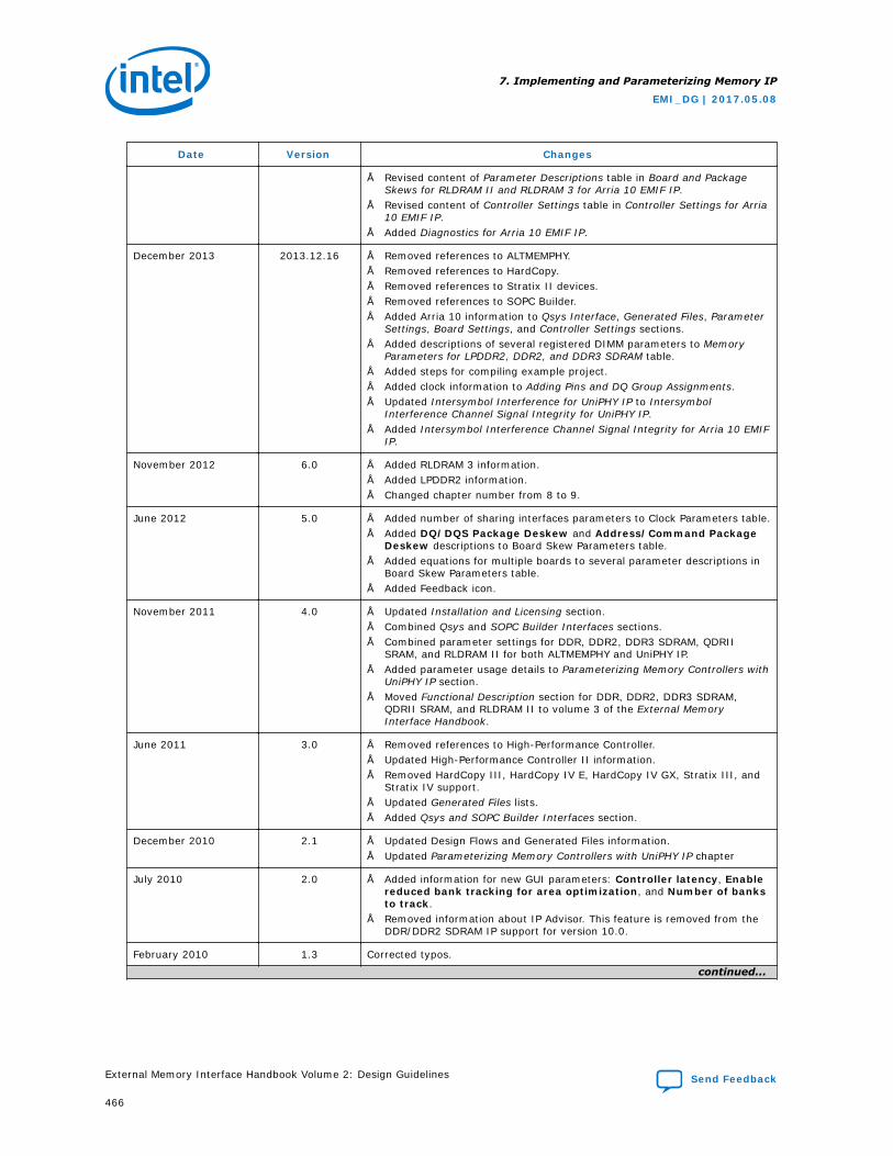
Date Version Changes
• Revised content of Parameter Descriptions table in Board and PackageSkews for RLDRAM II and RLDRAM 3 for Arria 10 EMIF IP.
• Revised content of Controller Settings table in Controller Settings for Arria10 EMIF IP.
• Added Diagnostics for Arria 10 EMIF IP.
December 2013 2013.12.16 • Removed references to ALTMEMPHY.• Removed references to HardCopy.• Removed references to Stratix II devices.• Removed references to SOPC Builder.• Added Arria 10 information to Qsys Interface, Generated Files, Parameter
Settings, Board Settings, and Controller Settings sections.• Added descriptions of several registered DIMM parameters to Memory
Parameters for LPDDR2, DDR2, and DDR3 SDRAM table.• Added steps for compiling example project.• Added clock information to Adding Pins and DQ Group Assignments.• Updated Intersymbol Interference for UniPHY IP to Intersymbol
Interference Channel Signal Integrity for UniPHY IP.• Added Intersymbol Interference Channel Signal Integrity for Arria 10 EMIF
IP.
November 2012 6.0 • Added RLDRAM 3 information.• Added LPDDR2 information.• Changed chapter number from 8 to 9.
June 2012 5.0 • Added number of sharing interfaces parameters to Clock Parameters table.• Added DQ/DQS Package Deskew and Address/Command Package
Deskew descriptions to Board Skew Parameters table.• Added equations for multiple boards to several parameter descriptions in
Board Skew Parameters table.• Added Feedback icon.
November 2011 4.0 • Updated Installation and Licensing section.• Combined Qsys and SOPC Builder Interfaces sections.• Combined parameter settings for DDR, DDR2, DDR3 SDRAM, QDRII
SRAM, and RLDRAM II for both ALTMEMPHY and UniPHY IP.• Added parameter usage details to Parameterizing Memory Controllers with
UniPHY IP section.• Moved Functional Description section for DDR, DDR2, DDR3 SDRAM,
QDRII SRAM, and RLDRAM II to volume 3 of the External MemoryInterface Handbook.
June 2011 3.0 • Removed references to High-Performance Controller.• Updated High-Performance Controller II information.• Removed HardCopy III, HardCopy IV E, HardCopy IV GX, Stratix III, and
Stratix IV support.• Updated Generated Files lists.• Added Qsys and SOPC Builder Interfaces section.
December 2010 2.1 • Updated Design Flows and Generated Files information.• Updated Parameterizing Memory Controllers with UniPHY IP chapter
July 2010 2.0 • Added information for new GUI parameters: Controller latency, Enablereduced bank tracking for area optimization, and Number of banksto track.
• Removed information about IP Advisor. This feature is removed from theDDR/DDR2 SDRAM IP support for version 10.0.
February 2010 1.3 Corrected typos.
continued...
7. Implementing and Parameterizing Memory IP
EMI_DG | 2017.05.08
External Memory Interface Handbook Volume 2: Design Guidelines Send Feedback
466

Date Version Changes
February 2010 1.2 • Full support for Stratix IV devices.• Added timing diagrams for initialization and calibration stages for HPC.
November 2009 1.1 Minor corrections.
November 2009 1.0 Initial release.
7. Implementing and Parameterizing Memory IP
EMI_DG | 2017.05.08
Send Feedback External Memory Interface Handbook Volume 2: Design Guidelines
467
8. Simulating Memory IPTo simulate your design you require the following components:
• A simulator—The simulator must be any Intel-supported VHDL or Verilog HDLsimulator
• A design using one of Intel’s external memory IP
• An example driver (to initiate read and write transactions)
• A testbench and a suitable memory simulation model
The Intel External Memory Interface IP is not compatible with the Qsys TestbenchSystem generation feature. Instead, use the simulation example design of yourgenerated IP as a reference for how to create a simulatable design, completed with amemory interface, a memory model, and a traffic generator.
Memory Simulation Models
There are two types of memory simulation models that you can use:
• Intel-provided generic memory model.
The Quartus® Prime software generates this model together with the example designand this model adheres to all the memory protocol specifications. You canparameterize the generic memory model.
• Vendor-specific memory model.
Memory vendors such as Micron and Samsung provide simulation models for specificmemory components that you can download from their websites.
Note: Intel does not provide support for vendor-specific memory models.
8.1. Simulation Options
The following simulation options are available with the example testbench to improvesimulation speed:
• Full calibration—Calibrates the same way as in hardware, and includes all phase,delay sweeps, and centering on every data bit.
Note: Arria 10 EMIF full calibration simulation will be available in a future releaseof the Quartus Prime software.
• Quick calibration—Calibrates the read and write latency only, skipping per bitdeskew. (Not available for Arria 10 EMIF IP.)
• Skip calibration—Provides the fastest simulation. It loads the settings calculatedfrom the memory configuration and enters user mode.
EMI_DG | 2017.05.08
Send Feedback
Intel Corporation. All rights reserved. Intel, the Intel logo, Altera, Arria, Cyclone, Enpirion, MAX, Nios, Quartusand Stratix words and logos are trademarks of Intel Corporation or its subsidiaries in the U.S. and/or othercountries. Intel warrants performance of its FPGA and semiconductor products to current specifications inaccordance with Intel's standard warranty, but reserves the right to make changes to any products and servicesat any time without notice. Intel assumes no responsibility or liability arising out of the application or use of anyinformation, product, or service described herein except as expressly agreed to in writing by Intel. Intelcustomers are advised to obtain the latest version of device specifications before relying on any publishedinformation and before placing orders for products or services.*Other names and brands may be claimed as the property of others.
ISO9001:2015Registered
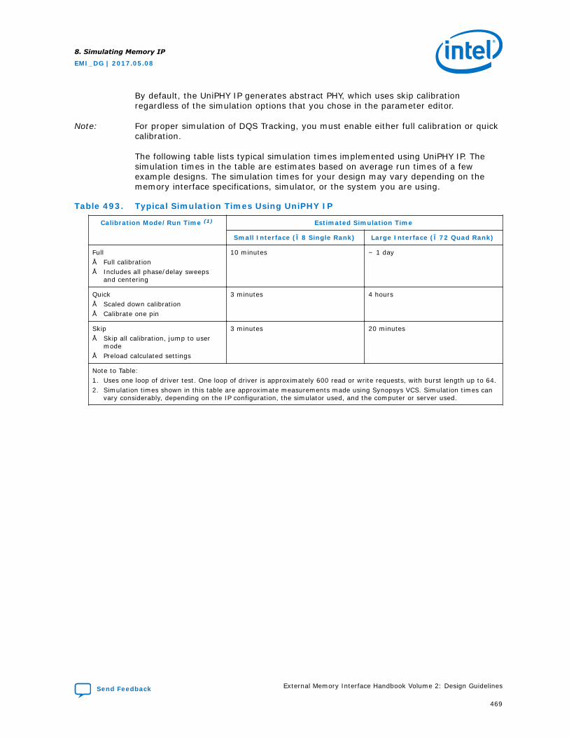
By default, the UniPHY IP generates abstract PHY, which uses skip calibrationregardless of the simulation options that you chose in the parameter editor.
Note: For proper simulation of DQS Tracking, you must enable either full calibration or quickcalibration.
The following table lists typical simulation times implemented using UniPHY IP. Thesimulation times in the table are estimates based on average run times of a fewexample designs. The simulation times for your design may vary depending on thememory interface specifications, simulator, or the system you are using.
Table 493. Typical Simulation Times Using UniPHY IP
Calibration Mode/Run Time (1) Estimated Simulation Time
Small Interface (×8 Single Rank) Large Interface (×72 Quad Rank)
Full• Full calibration• Includes all phase/delay sweeps
and centering
10 minutes ~ 1 day
Quick• Scaled down calibration• Calibrate one pin
3 minutes 4 hours
Skip• Skip all calibration, jump to user
mode• Preload calculated settings
3 minutes 20 minutes
Note to Table:1. Uses one loop of driver test. One loop of driver is approximately 600 read or write requests, with burst length up to 64.2. Simulation times shown in this table are approximate measurements made using Synopsys VCS. Simulation times can
vary considerably, depending on the IP configuration, the simulator used, and the computer or server used.
8. Simulating Memory IP
EMI_DG | 2017.05.08
Send Feedback External Memory Interface Handbook Volume 2: Design Guidelines
469
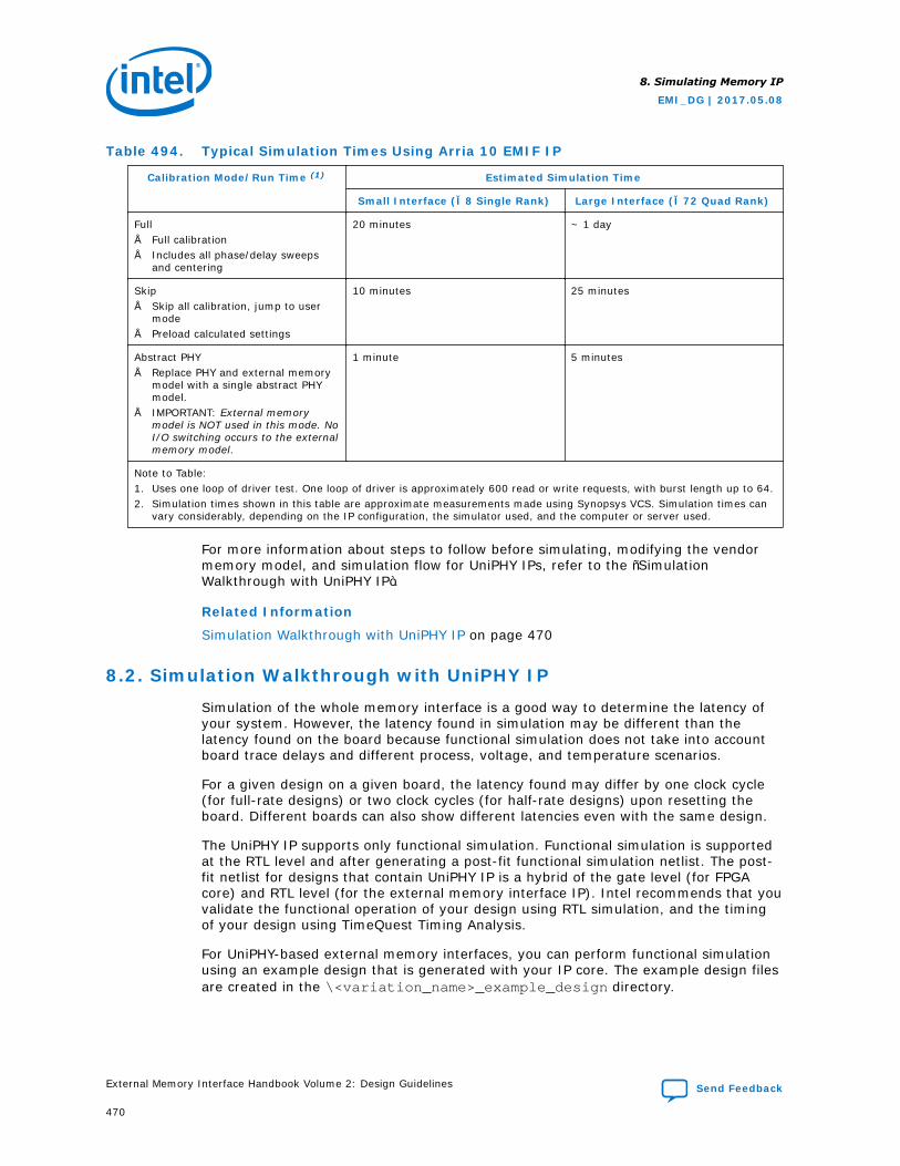
Table 494. Typical Simulation Times Using Arria 10 EMIF IP
Calibration Mode/Run Time (1) Estimated Simulation Time
Small Interface (×8 Single Rank) Large Interface (×72 Quad Rank)
Full• Full calibration• Includes all phase/delay sweeps
and centering
20 minutes ~ 1 day
Skip• Skip all calibration, jump to user
mode• Preload calculated settings
10 minutes 25 minutes
Abstract PHY• Replace PHY and external memory
model with a single abstract PHYmodel.
• IMPORTANT: External memorymodel is NOT used in this mode. NoI/O switching occurs to the externalmemory model.
1 minute 5 minutes
Note to Table:1. Uses one loop of driver test. One loop of driver is approximately 600 read or write requests, with burst length up to 64.2. Simulation times shown in this table are approximate measurements made using Synopsys VCS. Simulation times can
vary considerably, depending on the IP configuration, the simulator used, and the computer or server used.
For more information about steps to follow before simulating, modifying the vendormemory model, and simulation flow for UniPHY IPs, refer to the “SimulationWalkthrough with UniPHY IP”.
Related Information
Simulation Walkthrough with UniPHY IP on page 470
8.2. Simulation Walkthrough with UniPHY IP
Simulation of the whole memory interface is a good way to determine the latency ofyour system. However, the latency found in simulation may be different than thelatency found on the board because functional simulation does not take into accountboard trace delays and different process, voltage, and temperature scenarios.
For a given design on a given board, the latency found may differ by one clock cycle(for full-rate designs) or two clock cycles (for half-rate designs) upon resetting theboard. Different boards can also show different latencies even with the same design.
The UniPHY IP supports only functional simulation. Functional simulation is supportedat the RTL level and after generating a post-fit functional simulation netlist. The post-fit netlist for designs that contain UniPHY IP is a hybrid of the gate level (for FPGAcore) and RTL level (for the external memory interface IP). Intel recommends that youvalidate the functional operation of your design using RTL simulation, and the timingof your design using TimeQuest Timing Analysis.
For UniPHY-based external memory interfaces, you can perform functional simulationusing an example design that is generated with your IP core. The example design filesare created in the \<variation_name>_example_design directory.
8. Simulating Memory IP
EMI_DG | 2017.05.08
External Memory Interface Handbook Volume 2: Design Guidelines Send Feedback
470
You can use the IP functional simulation model with any supported VHDL or VerilogHDL simulator.
After you have generated the memory IP, view the README.txt file located in the\<variation_name>_example_design\simulation directory for instructions onhow to generate the simulation example design for Verilog HDL or VHDL. TheREADME.txt file also explains how to run simulation using the ModelSim - Intel FPGAEdition software. Simulation scripts for the Mentor Graphics, Cadence, Aldec, andSynopsys simulators are provided; however, detailed instructions on how to performsimulation using these third-party simulators are not provided.
8.2.1. Simulation Scripts
The Quartus Prime software generates three simulation scripts during projectgeneration for four different third party simulation tools—Cadence, Synopsys, Aldec,and Mentor Graphics.
The simulation scripts reduce the number of files that you need to compile separatelybefore simulating a design. These scripts are located in three separate folders underthe <project directory>\<varitation_name>_sim directory, each named afterthe names of the simulation tools. The example designs also provide equivalent scriptsafter you run the .tcl script from the project located in the\<variation_name>_example_design\simulation directory.
The order of the files in the simulation scripts is important. Ensure that you maintainthe files in order, to avoid error messages and warning messages during simulation. Ifyou choose not to use the Intel-generated simulation scripts in your simulationenvironment, you must maintain the specified file order when compiling the memorycontroller with the user-generated simulation script.
8.2.2. Preparing the Vendor Memory Model
You can replace the Intel-supplied memory model with a vendor-specific memorymodel. In general, you may find vendor-specific models to be standardized, thorough,and well supported, but sometimes more complex to setup and use.
Note: Intel does not provide support for vendor-specific memory models. If you do want toreplace the Intel-supplied memory model with a vendor-supplied memory model, youshould observe the following guidelines:
• Ensure that you have the correct vendor-supplied memory model for your memorydevice.
• Disconnect all signals from the default memory model and reconnect them to thevendor-supplied memory model.
• If you intend to run simulation from the Quartus Prime software, ensure that the .qip file points to the vendor-supplied memory model.
8. Simulating Memory IP
EMI_DG | 2017.05.08
Send Feedback External Memory Interface Handbook Volume 2: Design Guidelines
471

When you are using a vendor-supplied memory model instead of the generatedfunctional simulation model, you must modify the vendor memory model and thetestbench files by following these steps:
1. Obtain and copy the vendor memory model to the\<variation_name>_example_design\simulation\<variation_name>_sim\ submodules directory. For example, obtain the ddr2.v andddr2_parameters.vh simulation model files from the Micron website and savethem in the directory.
• The auto-generated generic SDRAM model may be used as a placeholder for aspecific vendor memory model.
• Some vendor DIMM memory models do not use data mask (DM) pin operation,which can cause calibration failures. In these cases, use the vendor’scomponent simulation models directly.
2. Open the vendor memory model file in a text editor and specify the speed gradeand device width at the top of the file. For example, you can add the followingstatements for a DDR2 SDRAM model file:
'define sg25
'define x8
The first statement specifies the memory device speed grade as –25 (for 400 MHzoperation). The second statement specifies the memory device width per DQS.
3. Check that the following statement is included in the vendor memory model file. Ifnot, include it at the top of the file. This example is for a DDR2 SDRAM model file:
`include "ddr2_parameters.vh"
4. Save the vendor memory model file.
5. Open the simulation example project file<variation_name>_example_sim.qpf, located in the<variation_name>_example_design\simulation directory.
6. On the Tools menu, select TCL scripts to run thegenerate_sim_verilog_example_design.tcl file, in which generates thesimulation example design.
7. To enable vendor memory model simulation, you have to include and compile thevendor memory model by adding it into the simulation script. Open the .tcl script,msim_setup.tcl, located in the <variation_name>_example_design\simulation\verilog\mentor directory in the text editor. Add in the followingline in the '# Compile the design files in correct order' section:
vlog +incdir+$QSYS_SIMDIR/submodules/ "$QSYS_SIMDIR/submodules/<vendor_memory>.v"-work <variation_name>_example_sim_work
8. Open the simulation example design, <variation_name>_example_sim.v,located in the <variation_name>_example_design\simulation\verilogdirectory in a text editor and delete the following module:
alt_mem_if_<memory_type>_mem_model_top_<memory_type>_mem_if_dm_pins_en_mem_if_dqsn_en
Note: The actual name of the pin may differ slightly depending on the memorycontroller you are using.
8. Simulating Memory IP
EMI_DG | 2017.05.08
External Memory Interface Handbook Volume 2: Design Guidelines Send Feedback
472
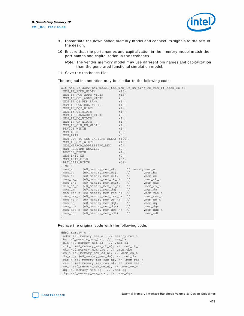
9. Instantiate the downloaded memory model and connect its signals to the rest ofthe design.
10. Ensure that the ports names and capitalization in the memory model match theport names and capitalization in the testbench.
Note: The vendor memory model may use different pin names and capitalizationthan the generated functional simulation model.
11. Save the testbench file.
The original instantiation may be similar to the following code:
alt_mem_if_ddr2_mem_model_top_mem_if_dm_pins_en_mem_if_dqsn_en #(.MEM_IF_ADDR_WIDTH (13),.MEM_IF_ROW_ADDR_WIDTH (12),.MEM_IF_COL_ADDR_WIDTH (8),.MEM_IF_CS_PER_RANK (1),.MEM_IF_CONTROL_WIDTH (1),.MEM_IF_DQS_WIDTH (1),.MEM_IF_CS_WIDTH (1),.MEM_IF_BANKADDR_WIDTH (3),.MEM_IF_DQ_WIDTH (8),.MEM_IF_CK_WIDTH (1),.MEM_IF_CLK_EN_WIDTH (1),.DEVICE_WIDTH (1),.MEM_TRCD (6),.MEM_TRTP (3),.MEM_DQS_TO_CLK_CAPTURE_DELAY (100),.MEM_IF_ODT_WIDTH (1),.MEM_MIRROR_ADDRESSING_DEC (0),.MEM_REGDIMM_ENABLED (0),.DEVICE_DEPTH (1),.MEM_INIT_EN (0),.MEM_INIT_FILE (""),.DAT_DATA_WIDTH (32)) m0 (.mem_a (e0_memory_mem_a), // memory.mem_a.mem_ba (e0_memory_mem_ba), // .mem_ba.mem_ck (e0_memory_mem_ck), // .mem_ck.mem_ck_n (e0_memory_mem_ck_n), // .mem_ck_n.mem_cke (e0_memory_mem_cke), // .mem_cke.mem_cs_n (e0_memory_mem_cs_n), // .mem_cs_n.mem_dm (e0_memory_mem_dm), // .mem_dm.mem_ras_n (e0_memory_mem_ras_n), // .mem_ras_n.mem_cas_n (e0_memory_mem_cas_n), // .mem_cas_n.mem_we_n (e0_memory_mem_we_n), // .mem_we_n.mem_dq (e0_memory_mem_dq), // .mem_dq.mem_dqs (e0_memory_mem_dqs), // .mem_dqs.mem_dqs_n (e0_memory_mem_dqs_n), // .mem_dqs_n.mem_odt (e0_memory_mem_odt) // .mem_odt);
Replace the original code with the following code:
ddr2 memory_0 (.addr (e0_memory_mem_a), // memory.mem_a.ba (e0_memory_mem_ba), // .mem_ba.clk (e0_memory_mem_ck), // .mem_ck.clk_n (e0_memory_mem_ck_n), // .mem_ck_n.cke (e0_memory_mem_cke), // .mem_cke.cs_n (e0_memory_mem_cs_n), // .mem_cs_n.dm_rdqs (e0_memory_mem_dm), // .mem_dm.ras_n (e0_memory_mem_ras_n), // .mem_ras_n.cas_n (e0_memory_mem_cas_n), // .mem_cas_n.we_n (e0_memory_mem_we_n), // .mem_we_n.dq (e0_memory_mem_dq), // .mem_dq.dqs (e0_memory_mem_dqs), // .mem_dqs
8. Simulating Memory IP
EMI_DG | 2017.05.08
Send Feedback External Memory Interface Handbook Volume 2: Design Guidelines
473
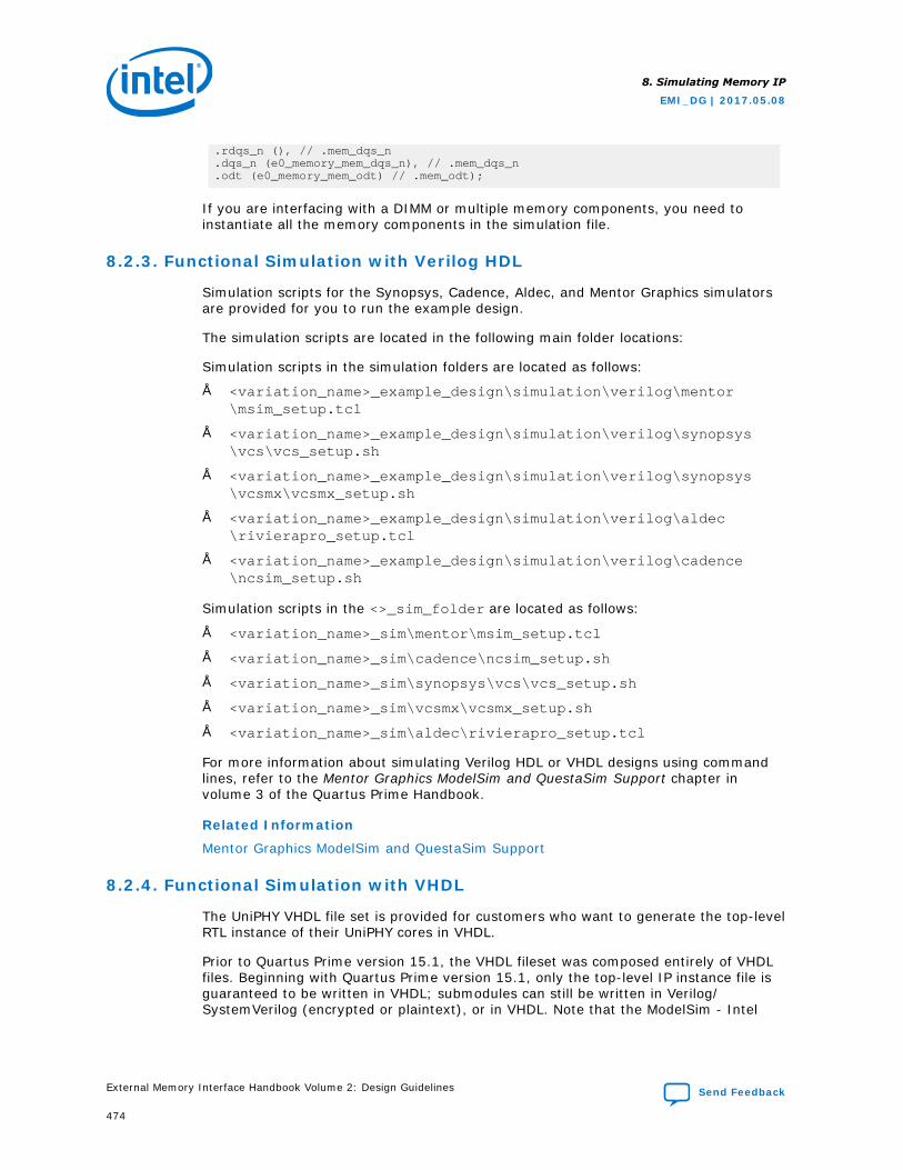
.rdqs_n (), // .mem_dqs_n
.dqs_n (e0_memory_mem_dqs_n), // .mem_dqs_n
.odt (e0_memory_mem_odt) // .mem_odt);
If you are interfacing with a DIMM or multiple memory components, you need toinstantiate all the memory components in the simulation file.
8.2.3. Functional Simulation with Verilog HDL
Simulation scripts for the Synopsys, Cadence, Aldec, and Mentor Graphics simulatorsare provided for you to run the example design.
The simulation scripts are located in the following main folder locations:
Simulation scripts in the simulation folders are located as follows:
• <variation_name>_example_design\simulation\verilog\mentor\msim_setup.tcl
• <variation_name>_example_design\simulation\verilog\synopsys\vcs\vcs_setup.sh
• <variation_name>_example_design\simulation\verilog\synopsys\vcsmx\vcsmx_setup.sh
• <variation_name>_example_design\simulation\verilog\aldec\rivierapro_setup.tcl
• <variation_name>_example_design\simulation\verilog\cadence\ncsim_setup.sh
Simulation scripts in the <>_sim_folder are located as follows:
• <variation_name>_sim\mentor\msim_setup.tcl
• <variation_name>_sim\cadence\ncsim_setup.sh
• <variation_name>_sim\synopsys\vcs\vcs_setup.sh
• <variation_name>_sim\vcsmx\vcsmx_setup.sh
• <variation_name>_sim\aldec\rivierapro_setup.tcl
For more information about simulating Verilog HDL or VHDL designs using commandlines, refer to the Mentor Graphics ModelSim and QuestaSim Support chapter involume 3 of the Quartus Prime Handbook.
Related Information
Mentor Graphics ModelSim and QuestaSim Support
8.2.4. Functional Simulation with VHDL
The UniPHY VHDL file set is provided for customers who want to generate the top-levelRTL instance of their UniPHY cores in VHDL.
Prior to Quartus Prime version 15.1, the VHDL fileset was composed entirely of VHDLfiles. Beginning with Quartus Prime version 15.1, only the top-level IP instance file isguaranteed to be written in VHDL; submodules can still be written in Verilog/SystemVerilog (encrypted or plaintext), or in VHDL. Note that the ModelSim - Intel
8. Simulating Memory IP
EMI_DG | 2017.05.08
External Memory Interface Handbook Volume 2: Design Guidelines Send Feedback
474
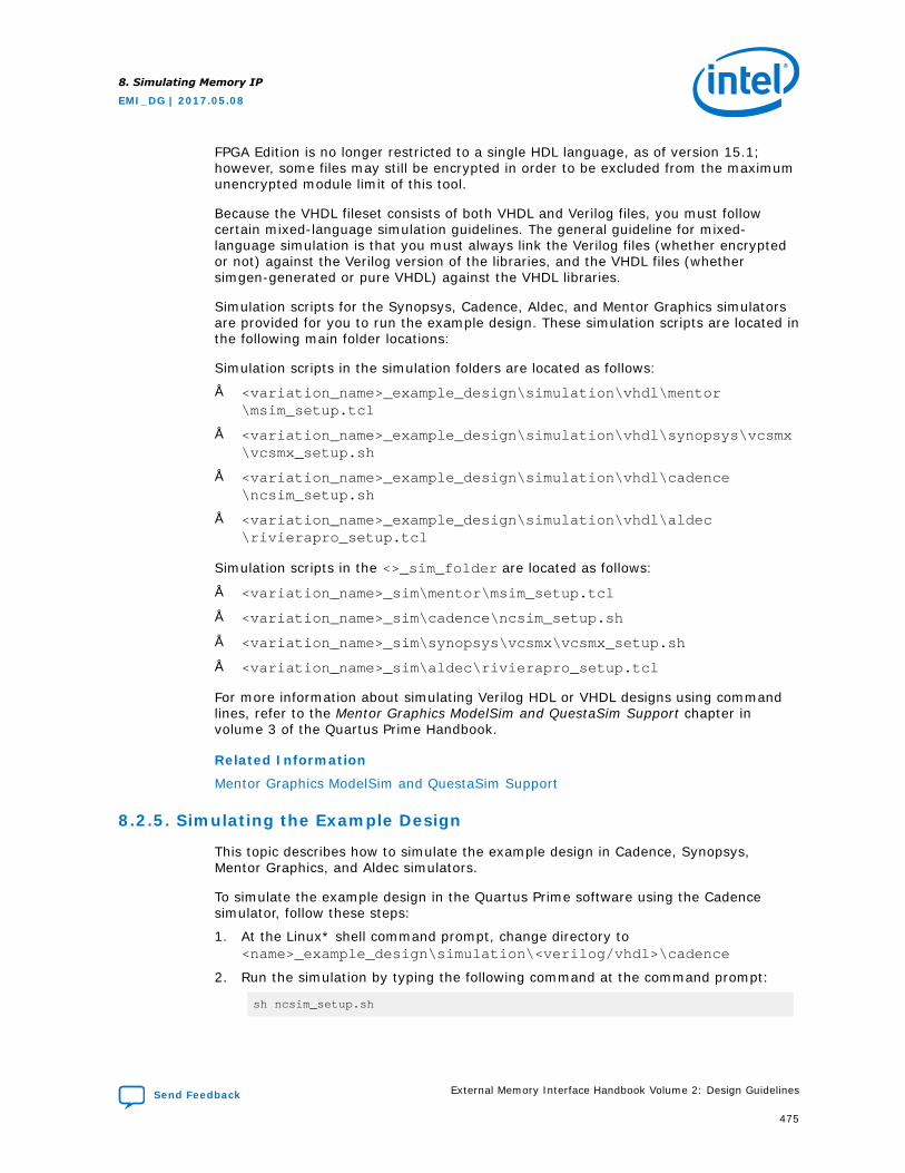
FPGA Edition is no longer restricted to a single HDL language, as of version 15.1;however, some files may still be encrypted in order to be excluded from the maximumunencrypted module limit of this tool.
Because the VHDL fileset consists of both VHDL and Verilog files, you must followcertain mixed-language simulation guidelines. The general guideline for mixed-language simulation is that you must always link the Verilog files (whether encryptedor not) against the Verilog version of the libraries, and the VHDL files (whethersimgen-generated or pure VHDL) against the VHDL libraries.
Simulation scripts for the Synopsys, Cadence, Aldec, and Mentor Graphics simulatorsare provided for you to run the example design. These simulation scripts are located inthe following main folder locations:
Simulation scripts in the simulation folders are located as follows:
• <variation_name>_example_design\simulation\vhdl\mentor\msim_setup.tcl
• <variation_name>_example_design\simulation\vhdl\synopsys\vcsmx\vcsmx_setup.sh
• <variation_name>_example_design\simulation\vhdl\cadence\ncsim_setup.sh
• <variation_name>_example_design\simulation\vhdl\aldec\rivierapro_setup.tcl
Simulation scripts in the <>_sim_folder are located as follows:
• <variation_name>_sim\mentor\msim_setup.tcl
• <variation_name>_sim\cadence\ncsim_setup.sh
• <variation_name>_sim\synopsys\vcsmx\vcsmx_setup.sh
• <variation_name>_sim\aldec\rivierapro_setup.tcl
For more information about simulating Verilog HDL or VHDL designs using commandlines, refer to the Mentor Graphics ModelSim and QuestaSim Support chapter involume 3 of the Quartus Prime Handbook.
Related Information
Mentor Graphics ModelSim and QuestaSim Support
8.2.5. Simulating the Example Design
This topic describes how to simulate the example design in Cadence, Synopsys,Mentor Graphics, and Aldec simulators.
To simulate the example design in the Quartus Prime software using the Cadencesimulator, follow these steps:
1. At the Linux* shell command prompt, change directory to<name>_example_design\simulation\<verilog/vhdl>\cadence
2. Run the simulation by typing the following command at the command prompt:
sh ncsim_setup.sh
8. Simulating Memory IP
EMI_DG | 2017.05.08
Send Feedback External Memory Interface Handbook Volume 2: Design Guidelines
475
To simulate the example design in the Quartus Prime software using the Synopsyssimulator, follow these steps:
1. At the Linux shell command prompt, change directory to<name>_example_design\simulation\<verilog/vhdl>\synopsys\vcsmx
2. Run the simulation by typing the following command at the command prompt:
sh vcsmx_setup.sh
To simulate the example design in the Quartus Prime software using the Mentorsimulator, follow these steps:
1. At the Linux or Windows shell command prompt, change directory to<name>_example_design\simulation\<verilog/vhdl>\mentor
2. Execute the msim_setup.tcl script that automatically compiles and runs thesimulation by typing the following command at the Linux or Windows commandprompt:
vsim -do run.do
or
Type the following command at the ModelSim command prompt:
do run.do
To simulate the example design in the Quartus Prime software using the Aldecsimulator, follow these steps:
1. At the Linux or Windows shell command prompt, change directory to<name>_example_design\simulation\<verilog/vhdl>\aldec
2. Execute the rivierapro_setup.tcl script that automatically compiles and runs thesimulation by typing the following command at the Linux or Windows commandprompt:vsim -do rivierapro.tcl
3. To compile and elaborate the design after the script loads, type ld_debug.
4. Type run -all to run the simulation.
For more information about simulation, refer to the Simulating Designs chapter involume 3 of the Quartus Prime Handbook.
If your Quartus Prime project appears to be configured correctly but the exampletestbench still fails, check the known issues on the Intel FPGA Knowledge Base beforefiling a service request.
Related Information
• Simulating Intel FPGA Designs
• Knowledge Database
8.2.6. UniPHY Abstract PHY Simulation
UniPHY IP generates both synthesizable and abstract models for simulation, with theabstract model as default. The UniPHY abstract model replaces the PLL with simplefixed-delay model, and the detailed models of the hard blocks with simple cycle-accurate functional models.
8. Simulating Memory IP
EMI_DG | 2017.05.08
External Memory Interface Handbook Volume 2: Design Guidelines Send Feedback
476
Full calibration mode cannot be used with abstract models, which is the default modeltype for all devices except Arria V and Cyclone V. In addition to enabling fullcalibration during generation, you must also disable the use of abstract models bymodifying the generated simulation scripts as described below. For VHDL, the UniPHYabstract model is the only option because you cannot switch to regular simulationmodel. The PLL frequencies in simulation may differ from the real time simulation dueto pico-second timing rounding.
However, you can switch to regular simulation models for Verilog HDL language. Thefull and quick calibration modes are available for regular simulation models.
Add an additional command line to the compilation script for the two relevant files toenable regular PHY simulation:
+define+ALTERA_ALT_MEM_IF_PHY_FAST_SIM_MODEL=0
The two relevant files are:
• In <variation_name>_example_design/simulation/verilog/submodules:
<variation_name>_example_sim_e0_if0_p0.sv
and
<variation_name>_example_sim_e0_if0_pll0.sv
or
• In <variation_name>_sim/submodules:
<variation_name>_p0.sv
and
<variation_name>_pll0.sv
To switch to regular simulation models for the Verilog HDL language on the examplesimulation design, follow the appropriate steps for your simulator:
• For the Mentor simulator, edit the msim_setup.tcl file as follows:
vlog - sv "$QSYS_SIMDIR/submodules/<variation_name>_example_sim_e0_if0_p0.sv”+define+ALTERA_ALT_MEM_IF_PHY_FAST_SIM_MODEL=0-work <variation_name>_example_sim_work
vlog - sv"$QSYS_SIMDIR/submodules/<variation_name>/_example_sim_e0_if0_pll0.sv"+define+ALTERA_ALT_MEM_IF_PHY_FAST_SIM_MODEL=0-work <variation_name>_example_sim_work
• For the Cadence simulator, edit the ncsim_setup.sh file as follows:
ncvlog- sv “$QSYS_SIMDIR/submodules/<variation_name>_example_sim_e0_if0_p0.sv"
8. Simulating Memory IP
EMI_DG | 2017.05.08
Send Feedback External Memory Interface Handbook Volume 2: Design Guidelines
477
+define+ALTERA_ALT_MEM_IF_PHY_FAST_SIM_MODEL=0-work <variation_name>_example_sim_work- cdslib ./cds_libs/skip_example_sim_work.cds.lib
ncvlog - sv "$QSYS_SIMDIR/submodules/<variation_name>_example_sim_e0_if0_pll0.sv"+define+ALTERA_ALT_MEM_IF_PHY_FAST_SIM_MODEL=0-work <variation_name>_example_sim_work- cdslib ./cds_libs/<variation_name>_example_sim_work.cds.lib
• For the Synopsys simulator, edit the vscmx_setup.sh file as follows:
vlogan +v2k - sverilog"$QSYS_SIMDIR/submodules/<variation_name>_example_sim_e0_if0_p0.sv"+define+ALTERA_ALT_MEM_IF_PHY_FAST_SIM_MODEL=0- work <variation_name>_example_sim_work
vlogan +v2k - sverilog"$QSYS_SIMDIR/submodules/<variation_name>_example_sim_e0_if0_pll0.sv"+define+ALTERA_ALT_MEM_IF_PHY_FAST_SIM_MODEL=0- work <variation_name>_example_sim_work
If you use the UniPHY abstract model, the simulation is two times faster in magnitudeif compared to the real simulation model. Instantiating a standalone UniPHY IP in yourdesign further improves the simulation time if you use a half-rate controller withUniPHY or a larger memory DQ width.
8.2.7. PHY-Only Simulation
To enable PHY-only simulation in the parameter editor, under PHY Settings tab, in theFPGA section, turn on Generate PHY only. This setting also applies to designs usingQsys. This option allows you to replace the Intel high-performance memory controllerswith your own custom controller.
When you are using a standard UniPHY memory interface, by default, the parametereditor generates an external memory interface with a controller and a PHY. Thecontroller and PHY are connected internally with the Altera PHY interface (AFI). Thememory interface has an Avalon slave port that connects to the controller to allowcommunication from the user logic. When you turn on the PHY-only option, theparameter editor generates the PHY without the controller. In this case, the PHY isaccessed via the AFI port, which can be externally connected to a custom controller. Inthe example design, a controller is instantiated externally to the memory interface.This provides a fully functional example design and demonstrates how to connect thecontroller to manage the transactions from the traffic generator.
The following figure shows the difference in the UniPHY memory interface when thePHY-only option is enabled.
8. Simulating Memory IP
EMI_DG | 2017.05.08
External Memory Interface Handbook Volume 2: Design Guidelines Send Feedback
478
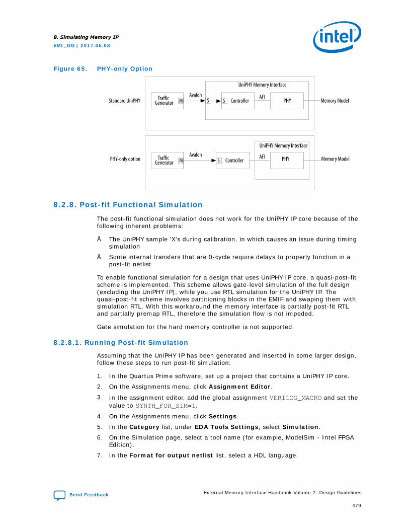
Figure 65. PHY-only Option
MAvalon
STraffic Generator
UniPHY Memory Interface
ControllerAFI
PHY
MAvalon
STraffic Generator
UniPHY Memory Interface
ControllerAFI PHY
Memory Model
Memory ModelPHY-only option
Standard UniPHY S
8.2.8. Post-fit Functional Simulation
The post-fit functional simulation does not work for the UniPHY IP core because of thefollowing inherent problems:
• The UniPHY sample 'X's during calibration, in which causes an issue during timingsimulation
• Some internal transfers that are 0-cycle require delays to properly function in apost-fit netlist
To enable functional simulation for a design that uses UniPHY IP core, a quasi-post-fitscheme is implemented. This scheme allows gate-level simulation of the full design(excluding the UniPHY IP), while you use RTL simulation for the UniPHY IP. Thequasi-post-fit scheme involves partitioning blocks in the EMIF and swaping them withsimulation RTL. With this workaround the memory interface is partially post-fit RTLand partially premap RTL, therefore the simulation flow is not impeded.
Gate simulation for the hard memory controller is not supported.
8.2.8.1. Running Post-fit Simulation
Assuming that the UniPHY IP has been generated and inserted in some larger design,follow these steps to run post-fit simulation:
1. In the Quartus Prime software, set up a project that contains a UniPHY IP core.
2. On the Assignments menu, click Assignment Editor.
3. In the assignment editor, add the global assignment VERILOG_MACRO and set thevalue to SYNTH_FOR_SIM=1.
4. On the Assignments menu, click Settings.
5. In the Category list, under EDA Tools Settings, select Simulation.
6. On the Simulation page, select a tool name (for example, ModelSim - Intel FPGAEdition).
7. In the Format for output netlist list, select a HDL language.
8. Simulating Memory IP
EMI_DG | 2017.05.08
Send Feedback External Memory Interface Handbook Volume 2: Design Guidelines
479

8. In the Output directory box, type or browse to the location where you wantoutput files saved.
9. Click More EDA Netlist Writer Settings to choose from a list of other options.
10. Set the value for Maintain hierarchy to PARTITION_ONLY, and click OK.
11. Elaborate the project. On the Processing menu, select Start and click StartHierarchy Elaboration.
12. In the Project Navigator window, click the Hierarchy tab. In the Entity box,locate the instances for the following devices:
a. For instances in Stratix III, Stratix IV, Arria II GX, Arria II GZ , click the + iconto expand the following top-level design entities, right-click on the lower-levelentities, select Design Partition, and click Set as Design Partition:
• <hierarchy path to UniPHY top-level>\<name>_if0:if0\<name>_if0_p0:p0
• <hierarchy path to UniPHY top-level>\<name>_if0:if0\<name>_if0_s0:s0
b. For instances in Arria V or Stratix V, click the + icon to expand the followingtop-level design entity, right-click on the lower-level entities, select DesignPartition, and click Set as Design Partition:
• <hierarchy path to UniPHY top-level>\<name>_if0:if0\<name>_if0_s0:s0
For instances of hard memory interfaces in Arria V, no design partition isnecessary.
13. In the Design Partitions Window, ensure that the netlist type value of thedesign partitions listed in Step12 a and 12b are set to Post-synthesis.
14. On the Processing menu, select Start and click Start Analysis and Synthesis.
15. Run the Pin assignments script. To run the pin assignment script, follow thesesteps:
a. On the Tools menu,click TCL Scripts.
b. In the Libraries list, locate the <name>_pin_assignment.tcl.
c. Click Run.
16. On the Processing menu, select Start and click Partition Merge.
17. On the Processing menu, select Start and click Start Fitter.
18. On the Processing menu, select Start and click Start EDA netlist writer .
19. The output post-fit netlist is located in the directory you chose in Step 8.
20. Assume that the netlist filename is dut.vo (or dut.vho for VHDL). Replace theinstance of the partitioned modules (specified in step 12) in dut.vo and instantiatethe original instance of the RTL. As a result, the RTL of those modules will simulatecorrectly instead of the the post-fit netlist. For example, you can delete thedefinition of the <name>_if0_s0 (and <name>_if0_p0, if appropriate)modules in the post-fit netlist, and ensure that your simulator compiles the post-fitnetlist and all the UniPHY RTL in order to properly link these modules forsimulation.
(This step does not apply to hard memory interfaces on Arria V devices.)
8. Simulating Memory IP
EMI_DG | 2017.05.08
External Memory Interface Handbook Volume 2: Design Guidelines Send Feedback
480
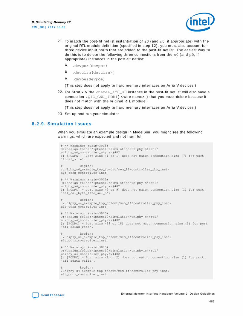
21. To match the post-fit netlist instantiation of s0 (and p0, if appropriate) with theoriginal RTL module definition (specified in step 12), you must also account forthree device input ports that are added to the post-fit netlist. The easiest way todo this is to delete the following three connections from the s0 (and p0, ifappropriate) instances in the post-fit netlist:
• .devpor(devpor)
• .devclrn(devclrn)(
• .devoe(devpoe)
(This step does not apply to hard memory interfaces on Arria V devices.)
22. For Stratix V the <name>_if0_s0 instance in the post-fit netlist will also have aconnection .QIC_GND_ PORT( <wire name> ) that you must delete because itdoes not match with the original RTL module.
(This step does not apply to hard memory interfaces on Arria V devices.)
23. Set up and run your simulator.
8.2.9. Simulation Issues
When you simulate an example design in ModelSim, you might see the followingwarnings, which are expected and not harmful:
# ** Warning: (vsim-3015) D:/design_folder/iptest10/simulation/uniphy_s4/rtl/uniphy_s4_controller_phy.sv(402): [PCDPC] - Port size (1 or 1) does not match connection size (7) for port'local_size'.
# Region: /uniphy_s4_example_top_tb/dut/mem_if/controller_phy_inst/alt_ddrx_controller_inst
# ** Warning: (vsim-3015) D:/design_folder/iptest10/simulation/uniphy_s4/rtl/uniphy_s4_controller_phy.sv(402): [PCDPC] - Port size (9 or 9) does not match connection size (1) for port'ctl_cal_byte_lane_sel_n'.
# Region: /uniphy_s4_example_top_tb/dut/mem_if/controller_phy_inst/alt_ddrx_controller_inst
# ** Warning: (vsim-3015) D:/design_folder/iptest10/simulation/uniphy_s4/rtl/uniphy_s4_controller_phy.sv(402): [PCDPC] - Port size (18 or 18) does not match connection size (1) for port'afi_doing_read'.
# Region: /uniphy_s4_example_top_tb/dut/mem_if/controller_phy_inst/alt_ddrx_controller_inst
# ** Warning: (vsim-3015)D:/design_folder/iptest10/simulation/uniphy_s4/rtl/uniphy_s4_controller_phy.sv(402): [PCDPC] - Port size (2 or 2) does not match connection size (1) for port'afi_rdata_valid'.
# Region: /uniphy_s4_example_top_tb/dut/mem_if/controller_phy_inst/alt_ddrx_controller_inst
8. Simulating Memory IP
EMI_DG | 2017.05.08
Send Feedback External Memory Interface Handbook Volume 2: Design Guidelines
481
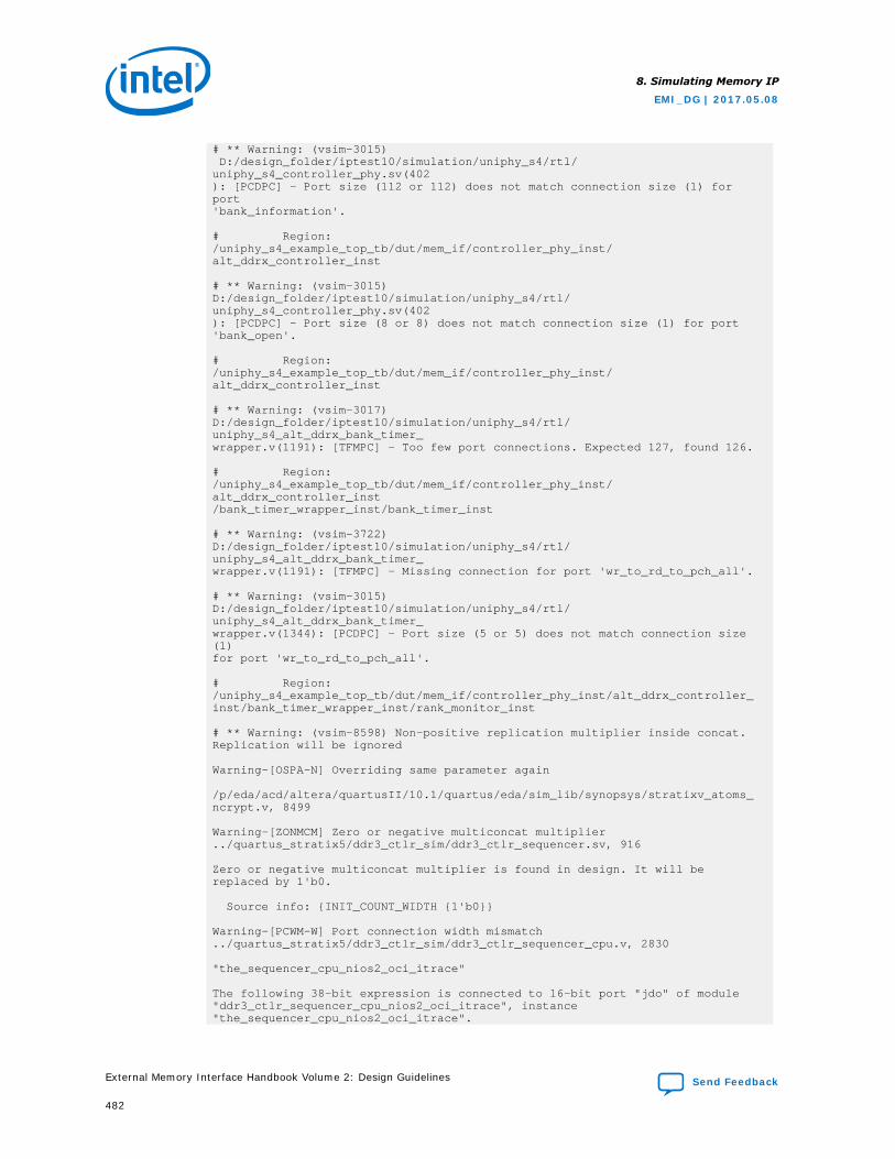
# ** Warning: (vsim-3015) D:/design_folder/iptest10/simulation/uniphy_s4/rtl/uniphy_s4_controller_phy.sv(402): [PCDPC] - Port size (112 or 112) does not match connection size (1) for port'bank_information'.
# Region: /uniphy_s4_example_top_tb/dut/mem_if/controller_phy_inst/alt_ddrx_controller_inst
# ** Warning: (vsim-3015) D:/design_folder/iptest10/simulation/uniphy_s4/rtl/uniphy_s4_controller_phy.sv(402): [PCDPC] - Port size (8 or 8) does not match connection size (1) for port'bank_open'.
# Region:/uniphy_s4_example_top_tb/dut/mem_if/controller_phy_inst/alt_ddrx_controller_inst
# ** Warning: (vsim-3017)D:/design_folder/iptest10/simulation/uniphy_s4/rtl/uniphy_s4_alt_ddrx_bank_timer_wrapper.v(1191): [TFMPC] - Too few port connections. Expected 127, found 126.
# Region: /uniphy_s4_example_top_tb/dut/mem_if/controller_phy_inst/alt_ddrx_controller_inst/bank_timer_wrapper_inst/bank_timer_inst
# ** Warning: (vsim-3722) D:/design_folder/iptest10/simulation/uniphy_s4/rtl/uniphy_s4_alt_ddrx_bank_timer_wrapper.v(1191): [TFMPC] - Missing connection for port 'wr_to_rd_to_pch_all'.
# ** Warning: (vsim-3015) D:/design_folder/iptest10/simulation/uniphy_s4/rtl/uniphy_s4_alt_ddrx_bank_timer_wrapper.v(1344): [PCDPC] - Port size (5 or 5) does not match connection size (1) for port 'wr_to_rd_to_pch_all'.
# Region: /uniphy_s4_example_top_tb/dut/mem_if/controller_phy_inst/alt_ddrx_controller_inst/bank_timer_wrapper_inst/rank_monitor_inst
# ** Warning: (vsim-8598) Non-positive replication multiplier inside concat. Replication will be ignored
Warning-[OSPA-N] Overriding same parameter again
/p/eda/acd/altera/quartusII/10.1/quartus/eda/sim_lib/synopsys/stratixv_atoms_ncrypt.v, 8499
Warning-[ZONMCM] Zero or negative multiconcat multiplier../quartus_stratix5/ddr3_ctlr_sim/ddr3_ctlr_sequencer.sv, 916
Zero or negative multiconcat multiplier is found in design. It will be replaced by 1'b0.
Source info: INIT_COUNT_WIDTH 1'b0
Warning-[PCWM-W] Port connection width mismatch ../quartus_stratix5/ddr3_ctlr_sim/ddr3_ctlr_sequencer_cpu.v, 2830
"the_sequencer_cpu_nios2_oci_itrace"
The following 38-bit expression is connected to 16-bit port "jdo" of module"ddr3_ctlr_sequencer_cpu_nios2_oci_itrace", instance "the_sequencer_cpu_nios2_oci_itrace".
8. Simulating Memory IP
EMI_DG | 2017.05.08
External Memory Interface Handbook Volume 2: Design Guidelines Send Feedback
482
Expression: jdouse +lint=PCWM for more details
8.3. Simulation Walkthrough with Arria 10 EMIF IP
Simulation of the whole memory interface is a good way to determine the latency ofyour system. However, the latency found in simulation may be different than thelatency found on the board because functional simulation does not take into accountboard trace delays and different process, voltage, and temperature scenarios.
For a given design on a given board, the latency found may differ by one clock cycle(for full-rate designs) or two clock cycles (for half-rate designs) upon resetting theboard. Different boards can also show different latencies even with the same design.
The Arria 10 EMIF IP supports only functional simulation. Functional simulation issupported at the RTL level and after generating a post-fit functional simulation netlist.The post-fit netlist for designs that contain Arria 10 EMIF IP is a hybrid of the gatelevel (for FPGA core) and RTL level (for the external memory interface IP). You shouldvalidate the functional operation of your design using RTL simulation, and the timingof your design using TimeQuest Timing Analysis.
For Arria 10 EMIF IP, you can perform functional simulation of an example design thatis generated with your IP core. The example design files are created in the\<variation_name>_example_design directory.
You can use the IP functional simulation model with any supported VHDL or VerilogHDL simulator.
After you have generated the memory IP, view the README. txt file located in the\<variation_name>_example_design directory for instructions on how togenerate the simulation example design for Verilog HDL or VHDL. Simulation filesetsfor both Verilog HDL and VHDL are located in\<variation_name>_example_design\sim. The README.txt file also explainshow to run simulation using the ModelSim - Intel FPGA Edition. Simulation scripts forthe Mentor Graphics, Cadence, Aldec, and Synopsys simulators are provided; however,detailed instructions on how to perform simulation using these third-party simulatorsare not provided.
8.3.1. Skip Calibration Versus Full Calibration
Calibration must occur shortly after the memory device is initialized, to compensatefor uncertainties of the hardware system, including silicon PVT variation, circuit boardtrace delays, and skewed arrival times. Such variations are usually not present in anRTL simulation environment, therefore there are two options for how the calibrationalgorithm behaves during simulation: Skip Calibration mode (which is the default),and Full Calibration mode.
Skip Calibration Mode
In Skip Calibration mode, the calibration processor assumes an ideal hardwareenvironment, where PVT variations, board delays, and trace skews are all zero.Instead of running the actual calibration routine, the calibration processor calculatesthe expected arrival time of read data based on the memory latency values that youprovide, thus reducing much simulation processing. Skip calibration mode is
8. Simulating Memory IP
EMI_DG | 2017.05.08
Send Feedback External Memory Interface Handbook Volume 2: Design Guidelines
483
recommended for use during system development, because it allows you to focus oninteracting with the controller and optimizing your memory access patterns, thusfacilitating rapid RTL development.
Full Calibration Mode
Full Calibration mode simulates every stage of the calibration algorithm immediatelyafter memory device initialization. Because the calibration algorithm processes eachdata group sequentially and each pin in each group individually, simulation timeincreases with the number of groups and data pins in your interface. You can observehow the calibration algorithm compensates for various delays in the system byincorporating your own board delay model based on trace delays from your PCBdesign tools. Due to the large simulation overhead, Full Calibration simulation mode isnot recommended for rapid development of IP cores.
VHDL Support
VHDL support for mixed-language simulators is implemented by generating the top-level wrapper for the core in VHDL, while all submodules are provided as clear textSystemVerilog files.
A set of precompiled device libraries is provided for use with the ModelSim - IntelFPGA Edition single-language simulator which is supplied with the Quartus Primesoftware. Submodules normally provided as cleartext SystemVerilog files areencrypted using IEEE Verilog HDL encryption for ModelSim - Intel FPGA Edition.
8.3.2. Arria 10 Abstract PHY Simulation
The abstract PHY is a simulation model of the EMIF PHY that can decrease simulationtime by 3-10 times. The abstract PHY replaces the lane and the external memorymodel with a single model containing an internal memory array. No switching of theI/Os to the external memory model occurs when simulating with the abstract PHY.
Abstract PHY reduces simulation time by two mechanisms:
• The Nios processor has been disabled and replaced by HDL forces that are appliedat the beginning of simulation. The HDL forces are a minimum set of configurationregisters that allow the EMIF to be configured properly for simulation. The writeand read latency values applied by the HDL forces are not representative of thepost-calibration values applied to the EMIF running on hardware. However, as longas the customer logic is avalon- and afi-compliant, these values allow forsuccessful RTL simulation.
• The abstract PHY eliminates the need for full-speed clocks and thereforesimulation of the abstract PHY does not require full-speed clock simulation events.
To use the abstract PHY, turn on Simulation Options Abstract PHY for fastsimulation on the Diagnostic tab. When you turn on the abstract PHY, the EMIF IP isconfigured as shown below. The PHY RTL and external memory model aredisconnected from the data path and in their place is the abstract PHY containing aninternal memory array. The abstract PHY is designed with no high-speed clocks,resulting in the removal of all high-speed clock simulator events.
8. Simulating Memory IP
EMI_DG | 2017.05.08
External Memory Interface Handbook Volume 2: Design Guidelines Send Feedback
484
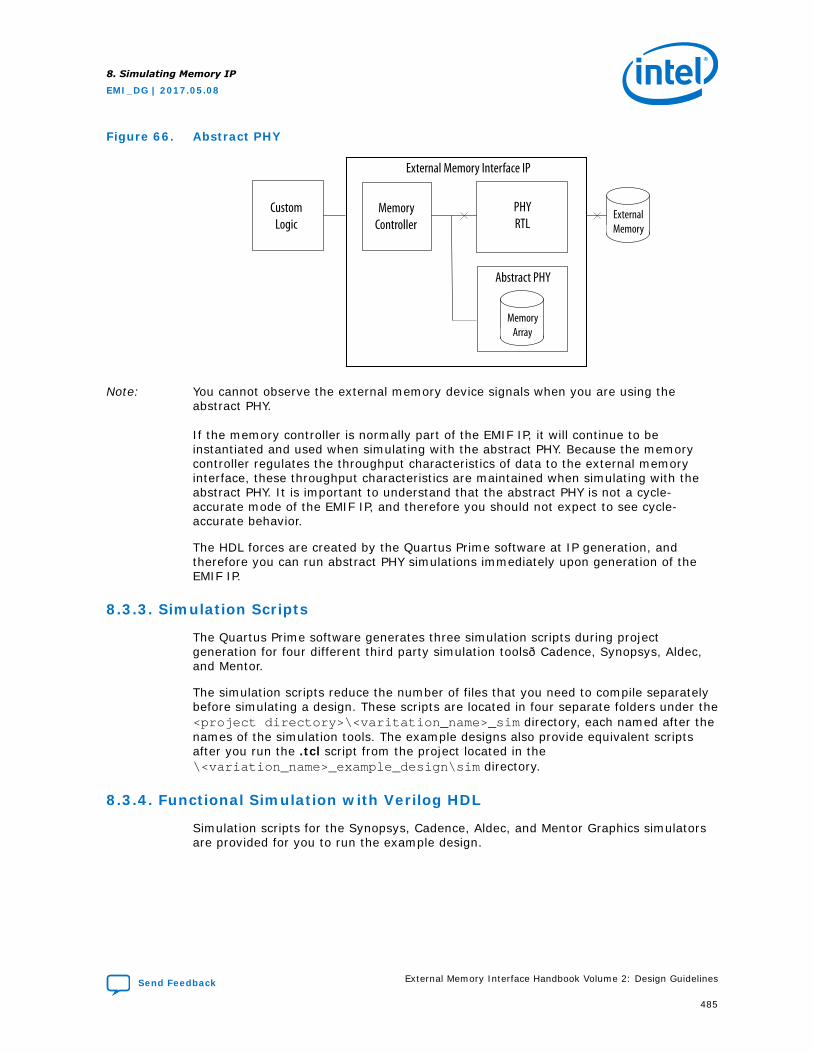
Figure 66. Abstract PHY
Abstract PHY
PHYRTL
MemoryArray
ExternalMemory
MemoryController
CustomLogic
External Memory Interface IP
Note: You cannot observe the external memory device signals when you are using theabstract PHY.
If the memory controller is normally part of the EMIF IP, it will continue to beinstantiated and used when simulating with the abstract PHY. Because the memorycontroller regulates the throughput characteristics of data to the external memoryinterface, these throughput characteristics are maintained when simulating with theabstract PHY. It is important to understand that the abstract PHY is not a cycle-accurate mode of the EMIF IP, and therefore you should not expect to see cycle-accurate behavior.
The HDL forces are created by the Quartus Prime software at IP generation, andtherefore you can run abstract PHY simulations immediately upon generation of theEMIF IP.
8.3.3. Simulation Scripts
The Quartus Prime software generates three simulation scripts during projectgeneration for four different third party simulation tools—Cadence, Synopsys, Aldec,and Mentor.
The simulation scripts reduce the number of files that you need to compile separatelybefore simulating a design. These scripts are located in four separate folders under the<project directory>\<varitation_name>_sim directory, each named after thenames of the simulation tools. The example designs also provide equivalent scriptsafter you run the .tcl script from the project located in the\<variation_name>_example_design\sim directory.
8.3.4. Functional Simulation with Verilog HDL
Simulation scripts for the Synopsys, Cadence, Aldec, and Mentor Graphics simulatorsare provided for you to run the example design.
8. Simulating Memory IP
EMI_DG | 2017.05.08
Send Feedback External Memory Interface Handbook Volume 2: Design Guidelines
485
The simulation scripts are located in the following main folder locations:
Simulation scripts in the simulation folders are located as follows:
• <variation_name>_example_design\sim\mentor\msim_setup.tcl
• <variation_name>_example_design\sim\synopsys\vcs\vcs_setup.sh
• <variation_name>_example_design\sim\synopsys\vcsmx\vcsmx_setup.sh
• <variation_name>_example_design\sim\aldec\rivierapro_setup.tcl
• <variation_name>_example_design\sim\cadence\ncsim_setup.sh
Simulation scripts in the <>_sim_folder are located as follows:
• <variation_name>_sim\mentor\msim_setup.tcl
• <variation_name>_sim\cadence\ncsim_setup.sh
• <variation_name>_sim\synopsys\vcs\vcs_setup.sh
• <variation_name>_sim\synopsys\vcsmx\vcsmx_setup.sh
• <variation_name>_sim\aldec\rivierapro_setup.tcl
For more information about simulating Verilog HDL or VHDL designs using commandlines, refer to the Mentor Graphics ModelSim and QuestaSim Support chapter involume 3 of the Quartus Prime Handbook.
Related Information
Mentor Graphics ModelSim and QuestaSim Support
8.3.5. Functional Simulation with VHDL
The Arria 10 EMIF VHDL fileset is provided for customers that wish to generate thetop-level RTL instance of their Arria 10 EMIF cores in VHDL.
Prior to Quartus Prime version 15.1, the VHDL fileset was comprised entirely of VHDLfiles. Beginning with Quartus Prime version 15.1, only the top-level IP instance file isguaranteed to be written in VHDL; submodules can still be deployed as Verilog/SystemVerilog (encrypted or plaintext) files, or VHDL files. Note that the ModelSim -Intel FPGA Edition is no longer restricted to a single HDL language as of Quartus 15.1;however, some files may still be encrypted in order to be excluded from the maximumunencrypted module limit of this tool.
Because the VHDL fileset consists of both VHDL and Verilog files, you must followcertain mixed-language simulation guidelines. The general guideline for mixed-language simulation is that you must always link the Verilog files (whether encryptedor not) against the Verilog version of the libraries, and the VHDL files (whetherSimGen-generated or pure VHDL) against the VHDL libraries.
8. Simulating Memory IP
EMI_DG | 2017.05.08
External Memory Interface Handbook Volume 2: Design Guidelines Send Feedback
486
Simulation scripts for the Synopsys, Cadence, Aldec, and Mentor Graphics simulatorsare provided for you to run the example design. These simulation scripts are located inthe following main folder locations:
Simulation scripts in the simulation folders are located as follows:
• <variation_name>_example_design\sim\mentor\msim_setup.tcl
• <variation_name>_example_design\sim\synopsys\vcsmx\vcsmx_setup.sh
• <variation_name>_example_design\sim\synopsys\vcs\vcs_setup.sh
• <variation_name>_example_design\sim\cadence\ncsim_setup.sh
• <variation_name>_example_design\sim\aldec\rivierapro_setup.tcl
Simulation scripts in the <>_sim_folder are located as follows:
• <variation_name>_sim\mentor\msim_setup.tcl
• <variation_name>_sim\cadence\ncsim_setup.sh
• <variation_name>_sim\synopsys\vcsmx\vcsmx_setup.sh
• <variation_name>_sim\aldec\rivierapro_setup.tcl
For more information about simulating Verilog HDL or VHDL designs using commandlines, refer to the Mentor Graphics ModelSim and QuestaSim Support chapter involume 3 of the Quartus Prime Handbook.
Related Information
Mentor Graphics ModelSim and QuestaSim Support
8.3.6. Simulating the Example Design
This topic describes how to simulate the example design in Cadence, Synopsys,Mentor Graphics, and Aldec simulators.
To simulate the example design in the Quartus Prime software using the Cadencesimulator, follow these steps:
1. At the Linux shell command prompt, change directory to<name>_example_design\sim\cadence
2. Run the simulation by typing the following command at the command prompt:
sh ncsim_setup.sh
To simulate the example design in the Quartus Prime software using the Synopsyssimulator, follow these steps:
1. At the Linux shell command prompt, change directory to<name>_example_design\sim\synopsys\vcsmx
2. Run the simulation by typing the following command at the command prompt:
sh vcsmx_setup.sh
8. Simulating Memory IP
EMI_DG | 2017.05.08
Send Feedback External Memory Interface Handbook Volume 2: Design Guidelines
487

To simulate the example design in the Quartus Prime software using the Mentorsimulator, follow these steps:
1. At the Linux or Windows shell command prompt, change directory to<name>_example_design\sim\mentor
2. Execute the msim_setup.tcl script that automatically compiles and runs thesimulation by typing the following command at the Linux or Windows commandprompt:
vsim -do msim_setup.tcl
or
Type the following command at the ModelSim command prompt:
do msim_setup.tcl
Note: Intel does not provide the run.do file for the example design with the Arria 10 EMIFinterface.
To simulate the example design in the Quartus Prime software using the Aldecsimulator, follow these steps:
1. At the Linux or Windows shell command prompt, change directory to<name>_example_design\sim\aldec
2. Execute the rivierapro_setup.tcl script that automatically compiles and runs thesimulation by typing the following command at the Linux or Windows commandprompt:vsim -do rivierapro.tcl
3. To compile and elaborate the design after the script loads, type ld_debug.
4. Type run -all to run the simulation.
For more information about simulation, refer to the Simulating Designs chapter involume 3 of the Quartus Prime Handbook.
If your Quartus Prime project appears to be configured correctly but the exampletestbench still fails, check the known issues on the Intel FPGA Knowledge Base beforefiling a service request.
Related Information
• Simulating Intel FPGA Designs
• Knowledge Database
8.4. Simulation Walkthrough with Stratix 10 EMIF IP
Simulation of the whole memory interface is a good way to determine the latency ofyour system. However, the latency found in simulation may be different than thelatency found on the board because functional simulation does not take into accountboard trace delays and different process, voltage, and temperature scenarios.
For a given design on a given board, the latency found may differ by one clock cycle(for full-rate designs) or two clock cycles (for half-rate designs) upon resetting theboard. Different boards can also show different latencies even with the same design.
8. Simulating Memory IP
EMI_DG | 2017.05.08
External Memory Interface Handbook Volume 2: Design Guidelines Send Feedback
488
The Stratix 10 EMIF IP supports only functional simulation. Functional simulation issupported at the RTL level and after generating a post-fit functional simulation netlist.The post-fit netlist for designs that contain Stratix 10 EMIF IP is a hybrid of the gatelevel (for FPGA core) and RTL level (for the external memory interface IP). You shouldvalidate the functional operation of your design using RTL simulation, and the timingof your design using TimeQuest Timing Analysis.
For Stratix 10 EMIF IP, you can perform functional simulation of an example designthat is generated with your IP core. The example design files are created in the\<variation_name>_example_design directory.
You can use the IP functional simulation model with any supported VHDL or VerilogHDL simulator.
After you have generated the memory IP, view the README. txt file located in the\<variation_name>_example_design directory for instructions on how togenerate the simulation example design for Verilog HDL or VHDL. Simulation filesetsfor both Verilog HDL and VHDL are located in\<variation_name>_example_design\sim. The README.txt file also explainshow to run simulation using the ModelSim - Intel FPGA Edition. Simulation scripts forthe Mentor Graphics, Cadence, Aldec, and Synopsys simulators ae provided; however,detailed instructions on how to perform simulation using these third-party simulatorsare not provided.
8.4.1. Skip Calibration Versus Full Calibration
Calibration must occur shortly after the memory device is initialized, to compensatefor uncertainties of the hardware system, including silicon PVT variation, circuit boardtrace delays, and skewed arrival times. Such variations are usually not present in anRTL simulation environment, therefore there are two options for how the calibrationalgorithm behaves during simulation: Skip Calibration mode (which is the default),and Full Calibration mode.
Skip Calibration Mode
In Skip Calibration mode, the calibration processor assumes an ideal hardwareenvironment, where PVT variations, board delays, and trace skews are all zero.Instead of running the actual calibration routine, the calibration processor calculatesthe expected arrival time of read data based on the memory latency values that youprovide, thus reducing much simulation processing. Skip calibration mode isrecommended for use during system development, because it allows you to focus oninteracting with the controller and optimizing your memory access patterns, thusfacilitating rapid RTL development.
Full Calibration Mode
Full Calibration mode simulates every stage of the calibration algorithm immediatelyafter memory device initialization. Because the calibration algorithm processes eachdata group sequentially and each pin in each group individually, simulation timeincreases with the number of groups and data pins in your interface. You can observehow the calibration algorithm compensates for various delays in the system byincorporating your own board delay model based on trace delays from your PCBdesign tools. Due to the large simulation overhead, Full Calibration simulation mode isnot recommended for rapid development of IP cores.
8. Simulating Memory IP
EMI_DG | 2017.05.08
Send Feedback External Memory Interface Handbook Volume 2: Design Guidelines
489
VHDL Support
VHDL support for mixed-language simulators is implemented by generating the top-level wrapper for the core in VHDL, while all submodules are provided as clear textSystemVerilog files.
A set of precompiled device libraries is provided for use with the ModelSim - IntelFPGA Edition single-language simulator which is supplied with the Quartus Primesoftware. Submodules normally provided as cleartext SystemVerilog files areencrypted using IEEE Verilog HDL encryption for ModelSim - Intel FPGA Edition.
8.4.2. Simulation Scripts
The Quartus Prime software generates three simulation scripts during projectgeneration for four different third party simulation tools—Cadence, Synopsys, Aldec,and Mentor.
The simulation scripts reduce the number of files that you need to compile separatelybefore simulating a design. These scripts are located in four separate folders under the<project directory>\<varitation_name>_sim directory, each named after thenames of the simulation tools. The example designs also provide equivalent scriptsafter you run the .tcl script from the project located in the\<variation_name>_example_design\sim directory.
8.4.3. Functional Simulation with Verilog HDL
Simulation scripts for the Synopsys, Cadence, Aldec, and Mentor Graphics simulatorsare provided for you to run the example design.
The simulation scripts are located in the following main folder locations:
Simulation scripts in the simulation folders are located as follows:
• <variation_name>_example_design\sim\mentor\msim_setup.tcl
• <variation_name>_example_design\sim\synopsys\vcs\vcs_setup.sh
• <variation_name>_example_design\sim\synopsys\vcsmx\vcsmx_setup.sh
• <variation_name>_example_design\sim\aldec\rivierapro_setup.tcl
• <variation_name>_example_design\sim\cadence\ncsim_setup.sh
Simulation scripts in the <>_sim_folder are located as follows:
• <variation_name>_sim\mentor\msim_setup.tcl
• <variation_name>_sim\cadence\ncsim_setup.sh
• <variation_name>_sim\synopsys\vcs\vcs_setup.sh
• <variation_name>_sim\synopsys\vcsmx\vcsmx_setup.sh
• <variation_name>_sim\aldec\rivierapro_setup.tcl
For more information about simulating Verilog HDL or VHDL designs using commandlines, refer to the Mentor Graphics ModelSim and QuestaSim Support chapter involume 3 of the Quartus Prime Handbook.
8. Simulating Memory IP
EMI_DG | 2017.05.08
External Memory Interface Handbook Volume 2: Design Guidelines Send Feedback
490
Related Information
Mentor Graphics ModelSim and QuestaSim Support
8.4.4. Functional Simulation with VHDL
The Stratix 10 EMIF VHDL fileset is provided for customers who want to generate thetop-level RTL instance of their Stratix 10 EMIF cores in VHDL.
The top-level IP instance file is guaranteed to be written in VHDL; submodules can bedeployed as Verilog/SystemVerilog (encrypted or plaintext) files, or VHDL files.ModelSim - Intel FPGA Edition is not restricted to a single HDL language; however,some files may be encrypted to be excluded from the maximum unencrypted modulelimit of this tool.
Because the VHDL fileset consists of both VHDL and Verilog files, you must followcertain mixed-language simulation guidelines. The general guideline for mixed-language simulation is that you must always link the Verilog files (whether encryptedor not) against the Verilog version of the libraries, and the VHDL files (whetherSimGen-generated or pure VHDL) against the VHDL libraries.
Simulation scripts for the Synopsys, Cadence, Aldec, and Mentor Graphics simulatorsare provided for you to run the example design. These simulation scripts are located inthe following main folder locations:
Simulation scripts in the simulation folders are located as follows:
• <variation_name>_example_design\sim\mentor\msim_setup.tcl
• <variation_name>_example_design\sim\synopsys\vcsmx\vcsmx_setup.sh
• <variation_name>_example_design\sim\synopsys\vcs\vcs_setup.sh
• <variation_name>_example_design\sim\cadence\ncsim_setup.sh
• <variation_name>_example_design\sim\aldec\rivierapro_setup.tcl
Simulation scripts in the <>_sim_folder are located as follows:
• <variation_name>_sim\mentor\msim_setup.tcl
• <variation_name>_sim\cadence\ncsim_setup.sh
• <variation_name>_sim\synopsys\vcsmx\vcsmx_setup.sh
• <variation_name>_sim\aldec\rivierapro_setup.tcl
For more information about simulating Verilog HDL or VHDL designs using commandlines, refer to the Mentor Graphics ModelSim and QuestaSim Support chapter involume 3 of the Quartus Prime Handbook.
8.4.5. Simulating the Example Design
This topic describes how to simulate the example design in Cadence, Synopsys,Mentor Graphics, and Aldec simulators.
8. Simulating Memory IP
EMI_DG | 2017.05.08
Send Feedback External Memory Interface Handbook Volume 2: Design Guidelines
491

To simulate the example design in the Quartus Prime software using the Cadencesimulator, follow these steps:
1. At the Linux shell command prompt, change directory to<name>_example_design\sim\cadence
2. Run the simulation by typing the following command at the command prompt:
sh ncsim_setup.sh
To simulate the example design in the Quartus Prime software using the Synopsyssimulator, follow these steps:
1. At the Linux shell command prompt, change directory to<name>_example_design\sim\synopsys\vcsmx
2. Run the simulation by typing the following command at the command prompt:
sh vcsmx_setup.sh
To simulate the example design in the Quartus Prime software using the Mentorsimulator, follow these steps:
1. At the Linux or Windows shell command prompt, change directory to<name>_example_design\sim\mentor
2. Execute the msim_setup.tcl script that automatically compiles and runs thesimulation by typing the following command at the Linux or Windows commandprompt:
vsim -do msim_setup.tcl
or
Type the following command at the ModelSim command prompt:
do msim_setup.tcl
Note: Intel does not provide the run.do file for the example design with the Stratix 10 EMIFinterface.
To simulate the example design in the Quartus Prime software using the Aldecsimulator, follow these steps:
1. At the Linux or Windows shell command prompt, change directory to<name>_example_design\sim\aldec
2. Execute the rivierapro_setup.tcl script that automatically compiles and runs thesimulation by typing the following command at the Linux or Windows commandprompt:vsim -do rivierapro.tcl
3. To compile and elaborate the design after the script loads, type ld_debug.
4. Type run -all to run the simulation.
For more information about simulation, refer to the Simulating Designs chapter involume 3 of the Quartus Prime Handbook.
If your Quartus Prime project appears to be configured correctly but the exampletestbench still fails, check the known issues on the Intel FPGA Knowledge Base beforefiling a service request.
8. Simulating Memory IP
EMI_DG | 2017.05.08
External Memory Interface Handbook Volume 2: Design Guidelines Send Feedback
492
8.5. Document Revision History
Date Version Changes
May 2017 2017.05.08 • Added Simulation Walkthrough with Stratix 10 EMIF IP section.• Rebranded as Intel.
October 2016 2016.10.31 Maintenance release.
May 2016 2016.05.02 • Added paragraph about incompatibility with the Qsys Testbench Systemgeneration feature to Simulating Memory IP.
• Updated Simulation Options and Abstract PHY Simulation topics forchanges to Abstract PHY.
• Added note to tables 10-1 and 10-2.• Updated Functional Simulation with VHDL topic in both Simulation
Walkthrough with UniPHY IP and Simulation Walkthrough with Arria 10EMIF IP sections.
November 2015 2015.11.02 • Added Abstract PHY Simulation topic.• Changed instances of Quartus II to Quartus Prime.
May 2015 2015.05.04 Maintenance release.
December 2014 2014.12.15 Maintenance release.
August 2014 2014.08.15 Removed references to MegaWizard Plug-In Manager.
December 2013 2013.12.16 • Removed references to ALTMEMPHY.• Removed references to HardCopy.• Removed references to SOPC Builder.• Added Simulation Walkthrough with Arria 10 EMIF IP.• Clarified explanation of full calibration mode with abstract models in
Abstract PHY section.
November 2012 6.0 Changed chapter number from 9 to 10.
June 2012 5.0 • Added path to simulation scripts for Riviera-PRO to Functional Simulationssection.
• Added simulation procedure for Riviera-PRO to Simulating the ExampleDesign section.
• Updated the Abstract PHY section.• Updated the Post-fit Functional Simulation procedure.• Added Feedback icon.
November 2011 4.0 • Added the PHY-Only Simulation section.• Added the Post-fit Functional Simulation section.• Updated the Simulation Walkthrough with UniPHY IP section.
June 2011 3.0 • Added an overview about memory simulation.• Added the Simulation Walkthrough with UniPHY IP section.
December 2010 2.1 Updated fr 10.1 release.
July 2010 2.0 Updated for 10.0 release.
January 2010 1.1 Corrected typos.
November 2009 1.0 Initial release.
8. Simulating Memory IP
EMI_DG | 2017.05.08
Send Feedback External Memory Interface Handbook Volume 2: Design Guidelines
493
9. Analyzing Timing of Memory IPThe external memory physical layer (PHY) interface offers a combination of source-synchronous and self-calibrating circuits to maximize system timing margins. Thephysical layer interface is a plug-and-play solution that the Quartus Prime TimeQuestTiming Analyzer timing constrains and analyzes.
The Intel FPGA IP and the numerous device features offered by Arria® II, Arria V, IntelArria 10, Cyclone® V, Stratix® III, Stratix IV, and Stratix V FPGAs, greatly simplify theimplementation of an external memory interface.
This chapter details the various timing paths that determine overall external memoryinterface performance, and describes the timing constraints and assumptions that thePHY IP uses to analyze these paths.
This chapter focuses on timing constraints for external memory interfaces based onthe UniPHY IP. For information about timing constraints and analysis of externalmemory interfaces and other source-synchronous interfaces based on the ALTDQ_DQSand ALTDQ_DQS2 IP cores, refer to AN 433: Constraining and Analyzing Source-Synchronous Interfaces and the Quartus Prime TimeQuest Timing Analyzer chapter involume 3 of the Quartus Prime Handbook.
External memory interface timing analysis is supported only by the TimeQuest TimingAnalyzer, for the following reasons:
• The wizard-generated timing constraint scripts support only the TimeQuestanalyzer.
• The Classic Timing Analyzer does not offer analysis of source-synchronousoutputs. For example, write data, address, and command outputs.
• The Classic Timing Analyzer does not support detailed rise and fall delay analysis.
The performance of an FPGA interface to an external memory device is dependent onthe following items:
• Read datapath timing
• Write datapath timing
• Address and command path timing
• Clock to strobe timing (tDQSS in DDR and DDR2 SDRAM, and tKHK#H in QDR II andQDRII+ SRAM)
• Read resynchronization path timing (applicable for DDR, DDR2, and DDR3 SDRAMin Arria II, Arria 10, Stratix III, Stratix IV, and Stratix V devices)
• Write leveling path timing (applicable for DDR2 and DDR3 SDRAM with UniPHY,and DDR3 and DDR4 SDRAM with Arria 10 EMIF IP.)
• PHY timing paths between I/O element and core registers
• PHY and controller internal timing paths (core fMAX and reset recovery/removal)
EMI_DG | 2017.05.08
Send Feedback
Intel Corporation. All rights reserved. Intel, the Intel logo, Altera, Arria, Cyclone, Enpirion, MAX, Nios, Quartusand Stratix words and logos are trademarks of Intel Corporation or its subsidiaries in the U.S. and/or othercountries. Intel warrants performance of its FPGA and semiconductor products to current specifications inaccordance with Intel's standard warranty, but reserves the right to make changes to any products and servicesat any time without notice. Intel assumes no responsibility or liability arising out of the application or use of anyinformation, product, or service described herein except as expressly agreed to in writing by Intel. Intelcustomers are advised to obtain the latest version of device specifications before relying on any publishedinformation and before placing orders for products or services.*Other names and brands may be claimed as the property of others.
ISO9001:2015Registered
• I/O toggle rate
• Output clock specifications
• Bus turnaround timing (applicable for RLDRAM II and DDR2 and DDR3 SDRAMwith UniPHY)
Note: External memory interface performance depends on various timing components, andoverall system level performance is limited by performance of the slowest link (that is,the path with the smallest timing margins).
Related Information
• AN 433: Constraining and Analyzing Source-Synchronous Interfaces
• Quartus Prime TimeQuest Timing Analyzer
9.1. Memory Interface Timing Components
There are several categories of memory interface timing components, includingsource-synchronous timing paths, calibrated timing paths, internal FPGA timing paths,and other FPGA timing parameters.
Understanding the nature of timing paths enables you to use an appropriate timinganalysis methodology and constraints. The following section examines these aspectsof memory interface timing paths.
9.1.1. Source-Synchronous Paths
Source-synchronous timing paths are those where clock and data signals pass fromthe transmitting device to the receiving device.
An example of a source-synchronous timing path is the FPGA-to-memory writedatapath. The FPGA device transmits DQ output data signals to the memory alongwith a center-aligned DQS output strobe signal. The memory device uses the DQSsignal to clock the data on the DQ pins into its internal registers.
Note: For brevity, the following topics refer to data signals and clock strobe signals as DQsignals and DQS signals, respectively. While the terminology is formally correct onlyfor DDR-type interfaces and does not match QDR II, QDR II+ and RLDRAM II pinnames, the behavior is similar enough that most timing properties and concepts applyto both. The clock that captures address and command signals is always referred to asCK/CK# too.
9.1.2. Calibrated Paths
Calibrated timing paths are those where the clock used to capture data is dynamicallypositioned within the data valid window (DVW) to maximize timing margin.
For UniPHY-based controllers and Arria 10 EMIF controllers, the sequencer blockanalyzes all path delays between the read capture registers and the read FIFO bufferto set up the FIFO write clock phase for optimal timing margin. The read postamblecalibration process is implemented in a similar manner to the read resynchonizationcalibration. In addition, the sequencer block calibrates a read data valid signal to thedelay between a controller issuing a read command and read data returning tocontroller.
9. Analyzing Timing of Memory IP
EMI_DG | 2017.05.08
Send Feedback External Memory Interface Handbook Volume 2: Design Guidelines
495
In DDR2, DDR3, and RLDRAM II with UniPHY, and in Arria 10 EMIF, the IP calibratesthe write-leveling chains and programmable output delay chain to align the DQS edgewith the CK edge at memory to meet the tDQSS, tDSS, and tDSH specifications.
Both UniPHY IP and Arria 10 EMIF IP enable the dynamic deskew calibration with theNios II sequencer for read and write paths. Dynamic deskew process uses theprogrammable delay chains that exist within the read and write data paths to adjustthe delay of each DQ and DQS pin to remove the skew between different DQ signalsand to centre-align the DQS strobe in the DVW of the DQ signals. This process occursat power up for the read and the write paths.
9.1.3. Internal FPGA Timing Paths
Other timing paths that have an impact on memory interface timing include FPGAinternal fMAX paths for PHY and controller logic.
This timing analysis is common to all FPGA designs. With appropriate timingconstraints on the design (such as clock settings), the TimeQuest Timing Analyzerreports the corresponding timing margins.
For more information about the TimeQuest Timing Analyzer, refer to the Quartus PrimeTimeQuest Timing Analyzer chapter in volume 3 of the Quartus Prime Handbook.
Related Information
Quartus Prime TimeQuest Timing Analyzer
9.1.4. Other FPGA Timing Parameters
Some FPGA data sheet parameters, such as I/O toggle rate and output clockspecifications, can limit memory interface performance.
I/O toggle rates vary based on speed grade, loading, and I/O bank location— top/bottom versus left/right. This toggle rate is also a function of the termination used(OCT or external termination) and other settings such as drive strength and slew rate.
Note: Ensure you check the I/O performance in the overall system performance calculation.Intel recommends that you perform signal integrity analysis for the specified drivestrength and output pin load combination.
For information about signal integrity, refer to the board design guidelines chaptersand AN 476: Impact of I/O Settings on Signal Integrity in Stratix III Devices.
Output clock specifications include clock period jitter, half-period jitter, cycle-to-cyclejitter, and skew between FPGA clock outputs. You can obtain these specifications fromthe FPGA data sheet and must meet memory device requirements. You can use thesespecifications to determine the overall data valid window for signals transmittedbetween the memory and FPGA device.
Related Information
AN 476: Impact of I/O Settings on Signal Integrity in Stratix III Devices
9. Analyzing Timing of Memory IP
EMI_DG | 2017.05.08
External Memory Interface Handbook Volume 2: Design Guidelines Send Feedback
496
9.2. FPGA Timing Paths
The following topics describe the FPGA timing paths, the timing constraints examples,and the timing assumptions that the constraint scripts use.
In Arria II, Arria V, Arria V GZ, Arria 10, Cyclone V, Stratix III, Stratix IV, and Stratix Vdevices, the interface margin is reported based on a combination of the TimeQuestTiming Analyzer and further steps to account for calibration that occurs at runtime.First the TimeQuest analyzer returns the base setup and hold slacks, and then furtherprocessing adjusts the slacks to account for effects which cannot be modeled inTimeQuest.
9.2.1. Arria II Device PHY Timing Paths
The following table lists all Arria II devices external memory interface timing paths.
Table 495. Arria II Devices External Memory Interface Timing Paths (1)
Timing Path Circuit Category Source Destination
Read Data (2) (6) Source-Synchronous Memory DQ, DQS Pins DQ Capture Registers in IOE
Write Data (2) (6) Source-Synchronous FPGA DQ, DQS Pins Memory DQ, DM, and DQSPins
Address and command (2) Source-Synchronous FPGA CK/CK# and Addr/CmdPins
Memory Input Pins
Clock-to-Strobe (2) Source-Synchronous FPGA CK/CK# and DQS OutputPins
Memory Input Pins
Read Resynchronization (2) Calibrated IOE Capture Registers IOE ResynchronizationRegisters
Read Resynchronization (2) (5) Calibrated IOE Capture Registers Read FIFO in FPGA Core
PHY IOE-Core Paths (2) Source-Synchronous IOE ResynchronizationRegisters
FIFO in FPGA Core
PHY and Controller Internal Paths (2)
Internal Clock fMAX Core Registers Core Registers
I/O Toggle Rate (3) I/O FPGA Output Pin Memory Input Pins
Output Clock Specifications(Jitter, DCD) (4)
I/O FPGA Output Pin Memory Input Pins
Notes to Table:1. Timing paths applicable for an interface between Arria II devices and SDRAM component.2. Timing margins for this path are reported by the TimeQuest Timing Analyzer Report DDR function.3. Intel recommends that you perform signal integrity simulations to verify I/O toggle rate.4. For output clock specifications, refer to the Arria II Device Data Sheet chapter of the Arria II Handbook.5. Only for UniPHY IP.6. Arria II GX devices use source-synchronous and calibrated path.
The following figure shows the Arria II GX devices input datapath registers and circuittypes.
Note: UniPHY IP interfaces bypass the synchronization registers.
9. Analyzing Timing of Memory IP
EMI_DG | 2017.05.08
Send Feedback External Memory Interface Handbook Volume 2: Design Guidelines
497
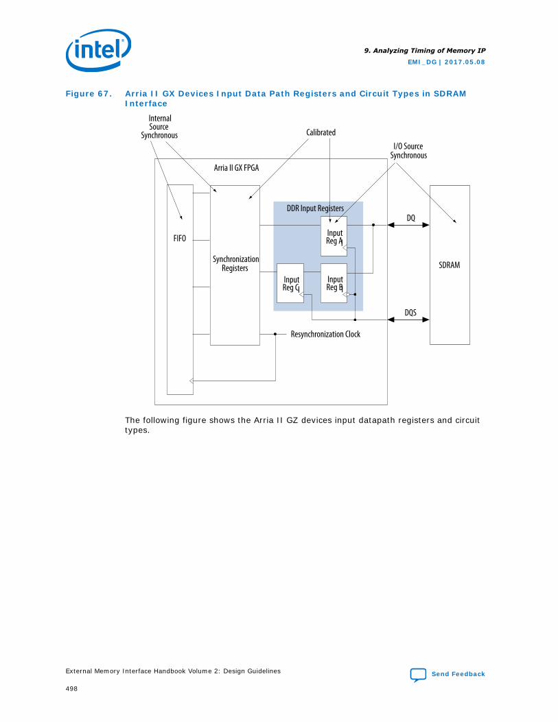
Figure 67. Arria II GX Devices Input Data Path Registers and Circuit Types in SDRAMInterface
Resynchronization Clock
SDRAM
DQ
Arria II GX FPGA
Internal Source
SynchronousI/O Source
Synchronous
Calibrated
DDR Input Registers
SynchronizationRegisters
FIFO
Input Reg CI
Input Reg BI
Input Reg AI
DQS
The following figure shows the Arria II GZ devices input datapath registers and circuittypes.
9. Analyzing Timing of Memory IP
EMI_DG | 2017.05.08
External Memory Interface Handbook Volume 2: Design Guidelines Send Feedback
498
Figure 68. Arria II GZ Devices Input Data Path Registers and Circuit Types in SDRAMInterface
Half-Rate Resynchronization Clock
SDRAM
DQ
Arria II GZ FPGA
I/O Source Synchronous and Calibrated
DDR Input Registers
FIFO
Input Reg CI
Input Reg BI
Input Reg AI
DQS
Related Information
Device Datasheet for Arria II Devices
9.2.2. Stratix III and Stratix IV PHY Timing Paths
A close look at all the register transfers occurring in the Stratix III and Stratix IV inputdatapath reveals many source-synchronous and calibrated circuits.
Note: The information in the following figure and table is based on Stratix IV devices, but isalso applicable to Stratix III devices.
The following figure shows a block diagram of this input path with some of these pathsidentified for Stratix IV devices. The output datapath contains a similar set of circuits.
Note: UniPHY IP interfaces bypass the alignment and synchronization registers.
9. Analyzing Timing of Memory IP
EMI_DG | 2017.05.08
Send Feedback External Memory Interface Handbook Volume 2: Design Guidelines
499
Figure 69. Stratix IV Input Path Registers and Circuit Types in SDRAM Interface
Resynchronization Clock
Half-Rate Resynchronization Clock
SDRAM
DQ
Stratix IV FPGA
Internal Source
SynchronousI/O Source
Synchronous and Calibrated
Calibrated
DDR Input Registers
Half-Rate Data Registers
Alignmentand
SynchronizationRegisters
FIFO
Input Reg C I
Input Reg BI
Input Reg AI
DQS
I/O Clock Divider
The following table lists the timing paths applicable for an interface between Stratix IVdevices and half-rate SDRAM components.
Note: The timing paths are also applicable to Stratix III devices, but Stratix III devices useonly source-synchronous path for read and write data paths.
Table 496. Stratix IV External Memory Interface Timing Paths (Part 1 of 2)
Timing Path Circuit Category Source Destination
Read Data (1) Source-Synchronous andCalibrated
Memory DQ, DQS Pins DQ Capture Registers inIOE
Write Data (1) Source-Synchronous andCalibrated
FPGA DQ, DQS Pins Memory DQ, DM, and DQSPins
Address and command (1) Source-Synchronous FPGA CK/CK# andAddr/Cmd Pins
Memory Input Pins
Clock-to-Strobe (1) Source-Synchronous FPGA CK/CK# and DQSOutput Pins
Memory Input Pins
Read Resynchronization (1) Calibrated IOE Capture Registers IOE Alignment andResynchronization Registers
Read Resynchronization (1) (4)
Calibrated IOE Capture Registers Read FIFO in FPGA Core
PHY IOE-Core Paths (1) Source-Synchronous IOE Half Data Rate Registersand Half-RateResynchronization Clock
FIFO in FPGA Core
PHY & Controller InternalPaths (1)
Internal Clock fMAX Core registers Core registers
continued...
9. Analyzing Timing of Memory IP
EMI_DG | 2017.05.08
External Memory Interface Handbook Volume 2: Design Guidelines Send Feedback
500
Timing Path Circuit Category Source Destination
I/O Toggle Rate (2) I/O – Data sheet FPGA Output Pin Memory Input Pins
Output Clock Specifications(Jitter, DCD) (3)
I/O – Data sheet FPGA Output Pin Memory Input Pins
Notes to Table:1. Timing margins for this path are reported by the TimeQuest Timing Analyzer Report DDR function.2. Intel recommends that you perform signal integrity simulations to verify I/O toggle rate.3. For output clock specifications, refer to theDC and Switching Characteristics chapter of the Stratix IV Device Handbook.4. Only for UniPHY IP.
Related Information
• DC and Switching Characteristics for Stratix III Devices
• DC and Switching Characteristics for Stratix IV Devices
9.2.3. Arria V, Arria V GZ, Arria 10, Cyclone V, and Stratix V Timing paths
The following figures show block diagrams of the input data paths for Arria V, Arria VGZ, Cyclone V, and Stratix V devices, and for Arria 10 devices.
Figure 70. Arria V, Arria V GZ, Cyclone V, and Stratix V Input Data Path
SDRAM
DQ
I/O Source Synchronous and Calibrated
DDR Input Registers
FIFO Input Reg C I
Input Reg BI
Input Reg AI
DQS
The following figure shows a block diagram of the Arria 10 input data path.
9. Analyzing Timing of Memory IP
EMI_DG | 2017.05.08
Send Feedback External Memory Interface Handbook Volume 2: Design Guidelines
501
Figure 71. Arria 10 Input Data Path
SDRAM
DQ
I/O Source Synchronous and Calibrated
DDR Input Registers
FIFOInput
Reg C IInput
Reg B I
Input Reg A I
DQS
I/O Lane
Delay Line
Delay Line
DQS
The following table lists all Arria V, Arria V GZ, Arria 10, Cyclone V, and Stratix Vdevices external memory interface timing paths.
Table 497. Arria V, Arria V GZ, Arria 10, Cyclone V, and Stratix V External MemoryInterface Timing Paths (1)
Timing Path Circuit Category Source Destination
Read Data (2) Source-Synchronous andCalibrated
Memory DQ, DQS Pins DQ Capture Registers inIOE
Write Data (2) Source-Synchronous andCalibrated
FPGA DQ, DM, DQSPins
Memory DQ, DM, andDQS Pins
Address and command (2) Source-Synchronous FPGA CK/CK# andAddr/Cmd Pins
Memory Input Pins
Clock-to-Strobe (2) Source-Synchronous FPGA CK/CK# andDQS Output Pins
Memory Input Pins
Read Resynchronization (2) Source-Synchronous IOE Capture Registers Read FIFO in IOE
PHY & Controller Internal Paths (2)
Internal Clock fMAX Core Registers Core Registers
continued...
9. Analyzing Timing of Memory IP
EMI_DG | 2017.05.08
External Memory Interface Handbook Volume 2: Design Guidelines Send Feedback
502
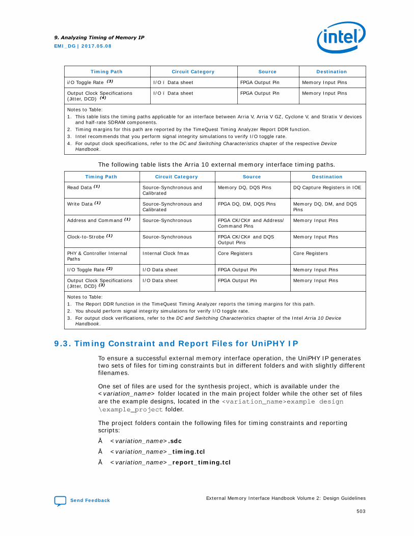
Timing Path Circuit Category Source Destination
i/O Toggle Rate (3) I/O – Data sheet FPGA Output Pin Memory Input Pins
Output Clock Specifications(Jitter, DCD) (4)
I/O – Data sheet FPGA Output Pin Memory Input Pins
Notes to Table:1. This table lists the timing paths applicable for an interface between Arria V, Arria V GZ, Cyclone V, and Stratix V devices
and half-rate SDRAM components.2. Timing margins for this path are reported by the TimeQuest Timing Analyzer Report DDR function.3. Intel recommends that you perform signal integrity simulations to verify I/O toggle rate.4. For output clock specifications, refer to the DC and Switching Characteristics chapter of the respective Device
Handbook.
The following table lists the Arria 10 external memory interface timing paths.
Timing Path Circuit Category Source Destination
Read Data (1) Source-Synchronous andCalibrated
Memory DQ, DQS Pins DQ Capture Registers in IOE
Write Data (1) Source-Synchronous andCalibrated
FPGA DQ, DM, DQS Pins Memory DQ, DM, and DQSPins
Address and Command (1) Source-Synchronous FPGA CK/CK# and Address/Command Pins
Memory Input Pins
Clock-to-Strobe (1) Source-Synchronous FPGA CK/CK# and DQSOutput Pins
Memory Input Pins
PHY & Controller InternalPaths
Internal Clock fmax Core Registers Core Registers
I/O Toggle Rate (2) I/O Data sheet FPGA Output Pin Memory Input Pins
Output Clock Specifications(Jitter, DCD) (3)
I/O Data sheet FPGA Output Pin Memory Input Pins
Notes to Table:1. The Report DDR function in the TimeQuest Timing Analyzer reports the timing margins for this path.2. You should perform signal integrity simulations for verify I/O toggle rate.3. For output clock verifications, refer to the DC and Switching Characteristics chapter of the Intel Arria 10 Device
Handbook.
9.3. Timing Constraint and Report Files for UniPHY IP
To ensure a successful external memory interface operation, the UniPHY IP generatestwo sets of files for timing constraints but in different folders and with slightly differentfilenames.
One set of files are used for the synthesis project, which is available under the<variation_name> folder located in the main project folder while the other set of filesare the example designs, located in the <variation_name>example design\example_project folder.
The project folders contain the following files for timing constraints and reportingscripts:
• <variation_name>.sdc
• <variation_name>_timing.tcl
• <variation_name>_report_timing.tcl
9. Analyzing Timing of Memory IP
EMI_DG | 2017.05.08
Send Feedback External Memory Interface Handbook Volume 2: Design Guidelines
503
• <variation_name>_report_timing_core.tcl
• <variation_name>_pin_map.tcl
• <variation_name>_parameters.tcl
<variation_name>.sdc
The <variation_name>.sdc is listed in the wizard-generated Quartus Prime IP File(.qip). Including this file in the project allows the Quartus Prime Synthesis and Fitterto use the timing driven compilation to optimize the timing margins.
To analyze the timing margins for all UniPHY timing paths, execute the Report DDRfunction in the TimeQuest Timing Analyzer.
The UniPHY IP uses the .sdc to constrain internal FPGA timing paths, address andcommand paths, and clock-to-strobe timing paths, and more specifically:
• Creating clocks on PLL inputs
• Creating generated clocks
• Calling derive_clock_uncertainty
• Cutting timing paths for specific reset paths
• Setting input and output delays on DQ inputs and outputs
• Setting output delays on address and command outputs (versus CK/CK# outputs)
<variation_name>_timing.tcl
This script includes the memory, FPGA, and board timing parameters for yourvariation. It is included within <variation_name>_report_timing.tcl and<variation_name>.sdc.
<variation_name>_report_timing.tcl
This script reports the timing slack for your variation. It runs automatically duringcompilation (during static timing analysis). You can also run this script with the ReportDDR task in the TimeQuest Timing Analyzer. This script is run for every instance of thesame variation.
<variation_name>_report_timing_core.tcl
This script contains high-level procedures that the<variation_name>_report_timing.tcl script uses to compute the timing slack foryour variation. This script runs automatically during compilation.
<variation_name>_pin_map.tcl
This script is a library of functions and procedures that the<variation_name>_report_timing.tcl and <variation_name> .sdc scripts use. The<variation_name>_pin_assignments.tcl script, which is not relevant to timingconstraints, also uses this library.
9. Analyzing Timing of Memory IP
EMI_DG | 2017.05.08
External Memory Interface Handbook Volume 2: Design Guidelines Send Feedback
504
<variation_name>_parameters.tcl
This script defines some of the parameters that describe the geometry of the core andthe PLL configuration. Do not change this file, except when you modify the PLLthrough the parameter editor. In this case, the changes to the PLL parameters do notautomatically propagate to this file and you must manually apply those changes in thisfile.
9.4. Timing Constraint and Report Files for Arria 10 EMIF IP
To ensure a successful external memory interface operation, the Arria 10 EMIF IPgenerates two sets of files for timing constraints but in different folders and withslightly different filenames.
One set of files are used for synthesis project, which is available under the<variation_name> folder located in the main project folder while the other set of filesare the example designs, located in the <variation_name>_example design\qiifolder.
The project folders contain the following files for timing constraints and reportingscripts:
• <variation_name>.sdc
• <variation_name>_ip_parameters.tcl
• <variation_name>_parameters.tcl
• <variation_name>_pin_map.tcl
• <variation_name>_report_timing.tcl
<variation_name>.sdc
The <variation_name>.sdc file is listed in the Quartus Prime IP File (.qip), which yougenerate by running make_qii_design.tcl. The <variation_name>.sdc file allows theQuartus Prime fitter to optimize timing margins with timing-driven compilation.
To analyze timing margins for all Arria 10 external memory interface IP timing paths,run the Report DDR function in the TimeQuest Timing Analyzer.
The Arria 10 EMIF IP uses the .sdc file for the following operations:
• Creating clocks on PLL inputs
• Creating generated clocks
• Calling derive_clock_uncertainty
• Creating a false path from a user clock to a hard memory controller clock, andvice versa
• Setting output delays on address and command outputs (versus CK/CK# outputs)
<variation_name>_ip_parameters.tcl
The <variation_name>_ip_parameters.tcl file is a script that lists the Arria 10 EMIFIP memory parameters and board parameters defined in the MegaWizard, which areused in the .sdc file and timing report scripts.
9. Analyzing Timing of Memory IP
EMI_DG | 2017.05.08
Send Feedback External Memory Interface Handbook Volume 2: Design Guidelines
505
<variation_name>_parameters.tclThe <variation_name>_parameters.tcl file is a script that lists the Arria 10 EMIF IPdevice and speed grade dependent values, which are used in the .sdc file and reporttiming scripts:
• Jitter
• Simultaneous switching noise
• Duty cycle distortion
• Calibration uncertainties
<variation_name>_pin_map.tcl
The <variation_name>_pin_map.tcl file is a library of functions and procedures thatthe <variation_name>report_timing.tcl and <variation_name>.sdc scripts use.
<variation_name>_report_timing.tcl
The <variation_name>_report_timing.tcl file is a script that contains timing analysisflow and reports the timing slack for your variation. This script runs automaticallyduring calibration (during static timing analysis) by sourcing the following files:
• <variation_name>_ip_parameters.tcl
• <variation_name>_parameters.tcl
• <variation_name>_pin_map.tcl
• <variation_name>_report_timing_core.tcl
You can also run <variation_name>_report_timing.tcl with the Report DDRfunction in the TimeQuest Timing Analyzer. This script runs for every instance of thesame variation.
<variation_name>_report_timing_core.tcl
The <variation_name>_report_timing_core.tcl file is a script that<variation_name>_report_timing.tcl uses to calculate the timing slack for yourvariation. <variation_name>_report_timing_core.tcl runs automatically duringcompilation.
<variation_name>_report_io_timing.tcl
The <variation_name>_report_io_timing.tcl file is a script that contains an earlyI/O estimation for your external memory interface design, excluding FPGA core timinganalysis. This script allows you to determine early I/O margins without having tocompile your design.
9.5. Timing Constraint and Report Files for Stratix 10 EMIF IP
To ensure a successful external memory interface operation, the Stratix 10 EMIF IPgenerates two sets of files for timing constraints but in different folders and withslightly different filenames.
One set of files are used for synthesis project, which is available under the<variation_name> folder located in the main project folder while the other set of filesare the example designs, located in the <variation_name>_example design\qii\ip folder.
9. Analyzing Timing of Memory IP
EMI_DG | 2017.05.08
External Memory Interface Handbook Volume 2: Design Guidelines Send Feedback
506
The project folders contain the following files for timing constraints and reportingscripts:
• <variation_name>.sdc
• <variation_name>_ip_parameters.tcl
• <variation_name>_parameters.tcl
• <variation_name>_pin_map.tcl
• <variation_name>_report_timing.tcl
<variation_name>.sdc
The <variation_name>.sdc file allows the Quartus Prime fitter to optimize timingmargins with timing-driven compilation.
To analyze timing margins for all Stratix 10 external memory interface IP timing paths,run the Report DDR function in the TimeQuest Timing Analyzer.
The Stratix 10 EMIF IP uses the .sdc file for the following operations:
• Creating clocks on PLL inputs
• Creating generated clocks
• Calling derive_clock_uncertainty
• Creating a false path from a user clock to a hard memory controller clock, andvice versa
• Setting output delays on address and command outputs (versus CK/CK# outputs)
<variation_name>_ip_parameters.tcl
The <variation_name>_ip_parameters.tcl file is a script that lists the Stratix 10EMIF IP memory parameters and board parameters defined in the MegaWizard, whichare used in the .sdc file and timing report scripts.
<variation_name>_parameters.tclThe <variation_name>_parameters.tcl file is a script that lists the Stratix 10 EMIF IPdevice and speed grade dependent values, which are used in the .sdc file and reporttiming scripts:
• Jitter
• Simultaneous switching noise
• Duty cycle distortion
• Calibration uncertainties
<variation_name>_pin_map.tcl
The <variation_name>_pin_map.tcl file is a library of functions and procedures thatthe <variation_name>report_timing.tcl and <variation_name>.sdc scripts use.
9. Analyzing Timing of Memory IP
EMI_DG | 2017.05.08
Send Feedback External Memory Interface Handbook Volume 2: Design Guidelines
507

<variation_name>_report_timing.tcl
The <variation_name>_report_timing.tcl file is a script that contains timing analysisflow and reports the timing slack for your variation. This script runs automaticallyduring calibration (during static timing analysis) by sourcing the following files:
• <variation_name>_ip_parameters.tcl
• <variation_name>_parameters.tcl
• <variation_name>_pin_map.tcl
• <variation_name>_report_timing_core.tcl
You can also run <variation_name>_report_timing.tcl with the Report DDRfunction in the TimeQuest Timing Analyzer. This script runs for every instance of thesame variation.
<variation_name>_report_timing_core.tcl
The <variation_name>_report_timing_core.tcl file is a script that<variation_name>_report_timing.tcl uses to calculate the timing slack for yourvariation. <variation_name>_report_timing_core.tcl runs automatically duringcompilation.
<variation_name>_report_io_timing.tcl
The <variation_name>_report_io_timing.tcl file is a script that contains an earlyI/O estimation for your external memory interface design, excluding FPGA core timinganalysis. This script allows you to determine early I/O margins without having tocompile your design.
9.6. Timing Analysis Description
The following sections describe the timing analysis using the respective FPGA datasheet specifications and the user-specified memory data sheet parameters.
9. Analyzing Timing of Memory IP
EMI_DG | 2017.05.08
External Memory Interface Handbook Volume 2: Design Guidelines Send Feedback
508
• Core to core (C2C) transfers have timing constraint created and are timinganalyzed by TimeQuest Analyzer. Core timing does not include user logic timingwithin core or to and from EMIF block. Both UniPHY-based IP and Arria 10 EMIF IPprovide the constrained clock to the customer logic.
• Core to periphery (C2P) transfers have timing constraint created and are timinganalyzed by TimeQuest Analyzer. This is common for UniPHY and Arria 10 ExternalMemory Interfaces IP. Because of the increased number of C2P/P2C signals in20nm families compared to previous families, more work is expected to ensurethat these special timing arcs are properly modeled, both during TimeQuest andcompilation.
• Periphery to core (P2C) transfers have timing constraint created and are timinganalyzed by TimeQuest Analyzer. This is common for UniPHY and Arria 10 ExternalMemory Interfaces IP. Because of the increased number of C2P/P2C signals in20nm families compared to previous families, more work is expected to ensurethat these special timing arcs are properly modeled, both during TimeQuest andcompilation.
• Periphery to periphery (P2P) transfers are modeled entirely by a minimum pulsewith violation on the hard block, and have no internal timing arc. In UniPHY-basedIP, P2P transfers are reported as part of Core Timing analysis. For Arria 10 EMIFIP, P2P transfers are modeled only by a minimum pulse width violation onhardened block.
To account for the effects of calibration, the UniPHY IP and Arria 10 EMIF IP includeadditional scripts that are part of the<phy_variation_name>_report_timing.tcl and <phy_variation_name>_report_timing_core.tcl files that determine the timing margin after calibration.These scripts use the setup and hold slacks of individual pins to emulate what isoccurring during calibration to obtain timing margins that are representative ofcalibrated PHYs. The effects considered as part of the calibrated timing analysisinclude improvements in margin because of calibration, and quantization error andcalibration uncertainty because of voltage and temperature changes after calibration.The calibration effects do not apply to Stratix III devices.
Related Information
Timing Constraint and Report Files for UniPHY IP on page 503
9.6.1. UniPHY IP Timing Analysis
The following topics describe timing analysis for UniPHY-based external memoryinterface IP.
9.6.1.1. Address and Command
Address and command signals are single data rate signals latched by the memorydevice using the FPGA output clock.
Some of the address and command signals are half-rate data signals, while others,such as the chip select, are full-rate signals. The TimeQuest Timing Analyzer analyzesthe address and command timing paths using the set_output_delay (max andmin) constraints.
9. Analyzing Timing of Memory IP
EMI_DG | 2017.05.08
Send Feedback External Memory Interface Handbook Volume 2: Design Guidelines
509
9.6.1.2. PHY or Core
Timing analysis of the PHY or core path includes the path of soft registers in thedevice and the register in the I/O element.
However, the analysis does not include the paths through the pin or the calibratedpath. The PHY or core analyzes this path by calling the report_timing command in<variation_name>_report_timing.tcl and<variation_name>_report_timing_core.tcl .
9.6.1.3. PHY or Core Reset
The PHY or core reset is the internal timing of the asynchronous reset signals to theUniPHY IP.
The PHY or core analyzes this path by calling the report_timing command in<variation_name>_report_timing.tcl and<variation_name>_report_timing_core.tcl.
9.6.1.4. Read Capture and Write
Stratix III memory interface designs perform read capture and write timing analysisusing the TCCS and SW timing specification.
Read capture and write timing analysis for Arria II, Cyclone IV, Stratix IV, and StratixV memory interface designs are based on the timing slacks obtained from theTimeQuest Timing Analyzer and all the effects included with the Quartus Prime timingmodel such as die-to-die and within-die variations, aging, systematic skew, andoperating condition variations. Because the PHY IP adjusts the timing slacks toaccount for the calibration effects, there are two sets of read capture and write timinganalysis numbers—Before Calibration and After Calibration.
9.6.1.4.1. Stratix III
This topic details the timing margins, such as the read data and write data timingpaths, which the TimeQuest Timing Analyzer callates for Stratix III designs. Timingpaths internal to the FPGA are either guaranteed by design and tested on silicon, oranalyzed by the TimeQuest Timing Analyzer using corresponding timing constraints.
For design guidelines about implementing and analyzing your external memoryinterface using the PHY in Stratix III and Stratix IV devices, refer to the designtutorials on the List of designs using Intel FPGA External Memory IP page ofwww.alterawiki.com.
Timing margins for chip-to-chip data transfers can be defined as:
Margin = bit period – transmitter uncertainties – receiver requirements
where:
• Sum of all transmitter uncertainties = transmitter channel-to-channel skew(TCCS).
The timing difference between the fastest and slowest output edges on datasignals, including tCO variation, clock skew, and jitter. The clock is included in theTCCS measurement and serves as the time reference.
9. Analyzing Timing of Memory IP
EMI_DG | 2017.05.08
External Memory Interface Handbook Volume 2: Design Guidelines Send Feedback
510
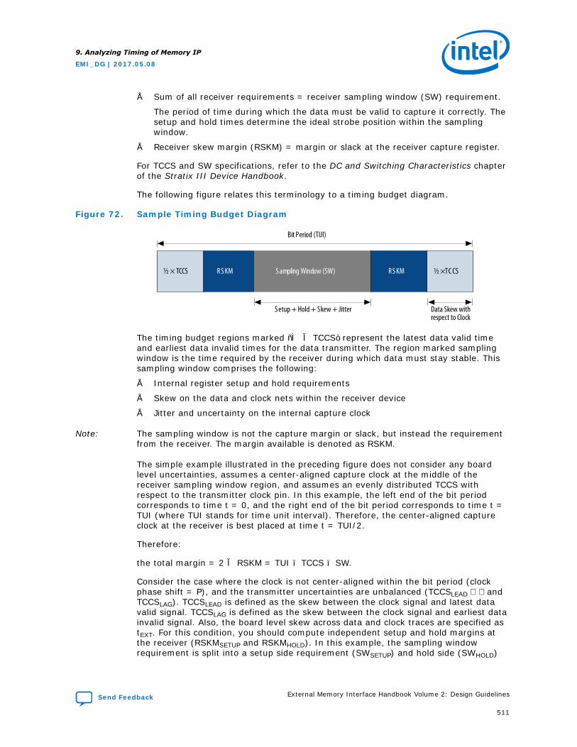
• Sum of all receiver requirements = receiver sampling window (SW) requirement.
The period of time during which the data must be valid to capture it correctly. Thesetup and hold times determine the ideal strobe position within the samplingwindow.
• Receiver skew margin (RSKM) = margin or slack at the receiver capture register.
For TCCS and SW specifications, refer to the DC and Switching Characteristics chapterof the Stratix III Device Handbook.
The following figure relates this terminology to a timing budget diagram.
Figure 72. Sample Timing Budget Diagram
½ × TCCS
Bit Period (TUI)
S etup + Hold + S kew + Jitter Data Skew with respect to Clock
S ampling Window (SW)
RS KM
RS KM
½ × TC CS
The timing budget regions marked “½ × TCCS” represent the latest data valid timeand earliest data invalid times for the data transmitter. The region marked samplingwindow is the time required by the receiver during which data must stay stable. Thissampling window comprises the following:
• Internal register setup and hold requirements
• Skew on the data and clock nets within the receiver device
• Jitter and uncertainty on the internal capture clock
Note: The sampling window is not the capture margin or slack, but instead the requirementfrom the receiver. The margin available is denoted as RSKM.
The simple example illustrated in the preceding figure does not consider any boardlevel uncertainties, assumes a center-aligned capture clock at the middle of thereceiver sampling window region, and assumes an evenly distributed TCCS withrespect to the transmitter clock pin. In this example, the left end of the bit periodcorresponds to time t = 0, and the right end of the bit period corresponds to time t =TUI (where TUI stands for time unit interval). Therefore, the center-aligned captureclock at the receiver is best placed at time t = TUI/2.
Therefore:
the total margin = 2 × RSKM = TUI – TCCS – SW.
Consider the case where the clock is not center-aligned within the bit period (clockphase shift = P), and the transmitter uncertainties are unbalanced (TCCSLEAD andTCCSLAG). TCCSLEAD is defined as the skew between the clock signal and latest datavalid signal. TCCSLAG is defined as the skew between the clock signal and earliest datainvalid signal. Also, the board level skew across data and clock traces are specified astEXT. For this condition, you should compute independent setup and hold margins atthe receiver (RSKMSETUP and RSKMHOLD). In this example, the sampling windowrequirement is split into a setup side requirement (SWSETUP) and hold side (SWHOLD)
9. Analyzing Timing of Memory IP
EMI_DG | 2017.05.08
Send Feedback External Memory Interface Handbook Volume 2: Design Guidelines
511
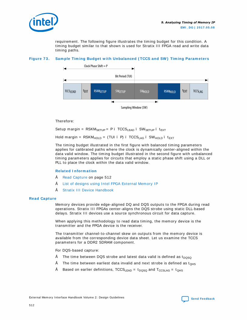
requirement. The following figure illustrates the timing budget for this condition. Atiming budget similar to that shown is used for Stratix III FPGA read and write datatiming paths.
Figure 73. Sample Timing Budget with Unbalanced (TCCS and SW) Timing Parameters
TCCSLEAD
SWSETUP SWHOLD
RSKMSETUP
RSKMHOLD
TCCSLAG
Sampling Window (SW)
Bit Period (TUI)
Clock Phase Shift = P
tEXT tEXT
Therefore:
Setup margin = RSKMSETUP = P – TCCSLEAD – SWSETUP – tEXT
Hold margin = RSKMHOLD = (TUI – P) – TCCSLAG – SWHOLD – tEXT
The timing budget illustrated in the first figure with balanced timing parametersapplies for calibrated paths where the clock is dynamically center-aligned within thedata valid window. The timing budget illustrated in the second figure with unbalancedtiming parameters applies for circuits that employ a static phase shift using a DLL orPLL to place the clock within the data valid window.
Related Information
• Read Capture on page 512
• List of designs using Intel FPGA External Memory IP
• Stratix III Device Handbook
Read CaptureMemory devices provide edge-aligned DQ and DQS outputs to the FPGA during readoperations. Stratix III FPGAs center-aligns the DQS strobe using static DLL-baseddelays. Stratix III devices use a source synchronous circuit for data capture.
When applying this methodology to read data timing, the memory device is thetransmitter and the FPGA device is the receiver.
The transmitter channel-to-channel skew on outputs from the memory device isavailable from the corresponding device data sheet. Let us examine the TCCSparameters for a DDR2 SDRAM component.
For DQS-based capture:
• The time between DQS strobe and latest data valid is defined as tDQSQ
• The time between earliest data invalid and next strobe is defined as tQHS
• Based on earlier definitions, TCCSLEAD = tDQSQ and TCCSLAG = tQHS
9. Analyzing Timing of Memory IP
EMI_DG | 2017.05.08
External Memory Interface Handbook Volume 2: Design Guidelines Send Feedback
512
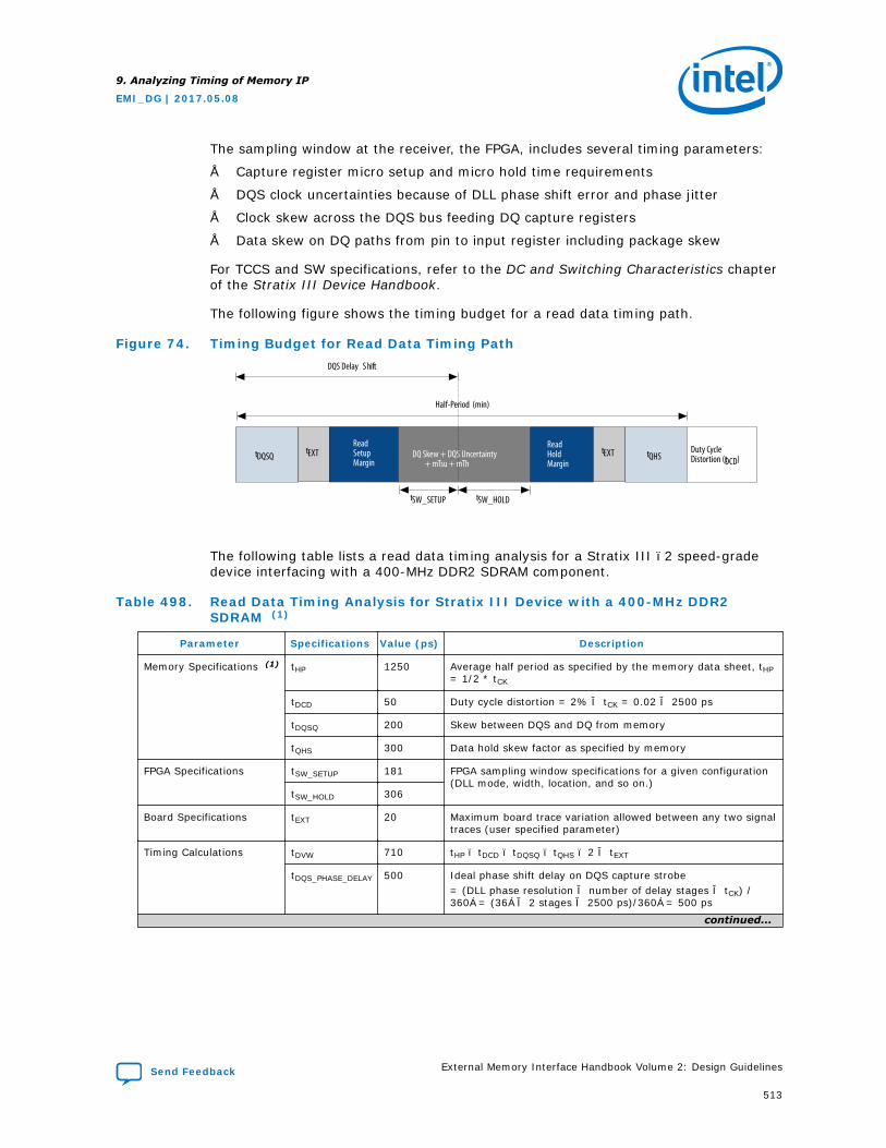
The sampling window at the receiver, the FPGA, includes several timing parameters:
• Capture register micro setup and micro hold time requirements
• DQS clock uncertainties because of DLL phase shift error and phase jitter
• Clock skew across the DQS bus feeding DQ capture registers
• Data skew on DQ paths from pin to input register including package skew
For TCCS and SW specifications, refer to the DC and Switching Characteristics chapterof the Stratix III Device Handbook.
The following figure shows the timing budget for a read data timing path.
Figure 74. Timing Budget for Read Data Timing Path
tDQSQ
Half-Period (min)
tSW_SETUP tSW_HOLD
DQ Skew + DQS Uncertainty + mTsu + mTh
Read Setup Margin
Read Hold Margin
tQHS
DQS Delay S hift
Duty Cycle Distortion (tDCD)
tEXT tEXT
The following table lists a read data timing analysis for a Stratix III –2 speed-gradedevice interfacing with a 400-MHz DDR2 SDRAM component.
Table 498. Read Data Timing Analysis for Stratix III Device with a 400-MHz DDR2SDRAM (1)
Parameter Specifications Value (ps) Description
Memory Specifications (1) tHP 1250 Average half period as specified by the memory data sheet, tHP= 1/2 * tCK
tDCD 50 Duty cycle distortion = 2% × tCK = 0.02 × 2500 ps
tDQSQ 200 Skew between DQS and DQ from memory
tQHS 300 Data hold skew factor as specified by memory
FPGA Specifications tSW_SETUP 181 FPGA sampling window specifications for a given configuration(DLL mode, width, location, and so on.)
tSW_HOLD 306
Board Specifications tEXT 20 Maximum board trace variation allowed between any two signaltraces (user specified parameter)
Timing Calculations tDVW 710 tHP – tDCD – tDQSQ – tQHS – 2 × tEXT
tDQS_PHASE_DELAY 500 Ideal phase shift delay on DQS capture strobe= (DLL phase resolution × number of delay stages × tCK) /360° = (36° × 2 stages × 2500 ps)/360° = 500 ps
continued...
9. Analyzing Timing of Memory IP
EMI_DG | 2017.05.08
Send Feedback External Memory Interface Handbook Volume 2: Design Guidelines
513
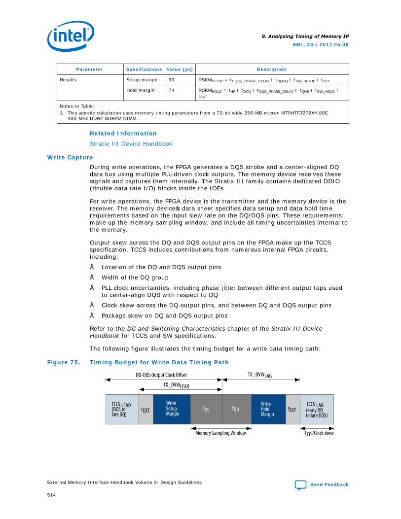
Parameter Specifications Value (ps) Description
Results Setup margin 99 RSKMSETUP = tDQSQ_PHASE_DELAY – tDQSQ – tSW_SETUP – tEXT
Hold margin 74 RSKMHOLD = tHP – tDCD – tDQS_PHASE_DELAY – tQHS – tSW_HOLD –tEXT
Notes to Table:1. This sample calculation uses memory timing parameters from a 72-bit wide 256-MB micron MT9HTF3272AY-80E
400-MHz DDR2 SDRAM DIMM.
Related Information
Stratix III Device Handbook
Write CaptureDuring write operations, the FPGA generates a DQS strobe and a center-aligned DQdata bus using multiple PLL-driven clock outputs. The memory device receives thesesignals and captures them internally. The Stratix III family contains dedicated DDIO(double data rate I/O) blocks inside the IOEs.
For write operations, the FPGA device is the transmitter and the memory device is thereceiver. The memory device’s data sheet specifies data setup and data hold timerequirements based on the input slew rate on the DQ/DQS pins. These requirementsmake up the memory sampling window, and include all timing uncertainties internal tothe memory.
Output skew across the DQ and DQS output pins on the FPGA make up the TCCSspecification. TCCS includes contributions from numerous internal FPGA circuits,including:
• Location of the DQ and DQS output pins
• Width of the DQ group
• PLL clock uncertainties, including phase jitter between different output taps usedto center-align DQS with respect to DQ
• Clock skew across the DQ output pins, and between DQ and DQS output pins
• Package skew on DQ and DQS output pins
Refer to the DC and Switching Characteristics chapter of the Stratix III DeviceHandbook for TCCS and SW specifications.
The following figure illustrates the timing budget for a write data timing path.
Figure 75. Timing Budget for Write Data Timing Path
TCCS LEAD (DQS to late DQ)
Memory Sampling Window
tDS
Write Setup Margin
Write Hold Margin
TX_DVWLEAD
tEXTtEXTTCCS LAG(early DQ to late DQS)
TX_DVWLAG
TCO /Clock skew
DQ-DQS Output Clock Offset
tDH
9. Analyzing Timing of Memory IP
EMI_DG | 2017.05.08
External Memory Interface Handbook Volume 2: Design Guidelines Send Feedback
514
The following table lists a write data timing analysis for a Stratix III –2 speed-gradedevice interfacing with a DDR2 SDRAM component at 400 MHz. This timing analysisassumes the use of a differential DQS strobe with 2.0-V/ns edge rates on DQS, and1.0-V/ns edge rate on DQ output pins. Consult your memory device’s data sheet forderated setup and hold requirements based on the DQ/DQS output edge rates fromyour FPGA.
.
Table 499. Write Data Timing Analysis for 400-MHz DDR2 SDRAM Stratix III Device (1)
Parameter Specifications Value (ps) Description
Memory Specifications (1) tHP 1250 Average half period as specified by the memory data sheet
tDSA 250 Memory setup requirement (derated for DQ/DQS edgerates and VREF reference voltage)
tDHA 250 Memory hold requirement (derated for DQ/DQS edge ratesand VREF reference voltage)
FPGA Specifications TCCSLEAD 229 FPGA transmitter channel-to-channel skew for a givenconfiguration (PLL setting, location, and width).
TCCSLAG 246
Board Specifications tEXT 20 Maximum board trace variation allowed between any twosignal traces (user specified parameter)
Timing Calculations tOUTPUT_CLOCK _OFFSET 625 Output clock phase offset between DQ & DQS outputclocks = 90°.tOUTPUT_CLOCK_OFFSET = (output clock phase DQ and DQSoffset x tCK)/360° = (90° x 2500)/360° = 625
TX_DVWLEAD 396 Transmitter data valid window = tOUTPUT_CLOCK_OFFSET –TCCSLEAD
TX_DVWLAG 379 Transmitter data valid window = tHP - tOUTPUT_CLOCK_OFFSET– TCCSLAG
Results Setup margin 126 TX_DVWLEAD – tEXT – tDSA
Hold margin 109 TX_DVWLAG – tEXT – tDHA
Notes to Table:1. This sample calculation uses memory timing parameters from a 72-bit wide 256-MB micron MT9HTF3272AY-80E 400-
MHz DDR2 SDRAM DIMM
Related Information
• Read Capture on page 512
• Stratix III Device Handbook
9.6.1.4.2. Arria II, Arria V, Cyclone V, Stratix IV and Stratix V
Read capture timing analysis indicates the amount of slack on the DDR DQ signals thatare latched by the FPGA using the DQS strobe output of the memory device.
Read Capture
The read capture timing paths are analyzed by a combination of the TimeQuest TimingAnalyzer using the set_input_delay (max and min), set_max_delay, andset_min_delay constraints, and further steps to account for calibration that occursat runtime. The UniPHY IP include timing constraints in the
9. Analyzing Timing of Memory IP
EMI_DG | 2017.05.08
Send Feedback External Memory Interface Handbook Volume 2: Design Guidelines
515
<phy_variation_name>.sdc file, and further slack analysis in<phy_variation_name>_report_timing.tcl and<phy_variation_name>_report_timing_core.tcl files.
In Arria II and Stratix IV devices, the margin is reported based on a combination ofthe TimeQuest Timing Analyzer calculation results and further processing steps thataccount for the calibration that occurs at runtime. First, the TimeQuest analyzerreturns the base setup and hold slacks, and further processing steps adjust the slacksto account for effects which the TimeQuest analyzer cannot model.
Write
Write timing analysis indicates the amount of slack on the DDR DQ signals that arelatched by the memory device using the DQS strobe output from the FPGA device. Thewrite timing paths are analyzed by a combination of the TimeQuest Timing Analyzerusing the set_output_delay (max and min) and further steps to account forcalibration that occurs at runtime. The UniPHY IP includes timing constraints in the<phy_variation_name>.sdc (UniPHY) file, and further slack analysis in the<phy_variation_name>_report_timing.tcl and<phy_variation_name>_report_timing_core.tcl files.
9.6.1.5. Read Resynchronization
In a UniPHY interface, a FIFO buffer synchronizes the data transfer from the datacapture to the core.
The calibration process sets the depth of the FIFO buffer and no dedicatedsynchronization clock is required. Refer to <phy_variation_name>_report_timing_core.tcl for more information about the resynchronization timingmargin equation.
9.6.1.6. DQS versus CK—Arria II GX and Cyclone IV Devices
The DQS versus CK timing path indicates the skew requirement for the arrival time ofthe DQS strobe at the memory with respect to the arrival time of CK/CK# at thememory. Arria II GX and Cyclone IV devices require the DQS strobes and CK clocks toarrive edge aligned.
There are two timing constraints for DQS versus CK timing path to account for dutycycle distortion. The DQS/DQS# rising edge to CK/CK# rising edge (tDQSS) requiresthe rising edge of DQS to align with the rising edge of CK to within 25% of a clockcycle, while the DQS/DQS# falling edge setup/hold time from CK/CK# rising edge(tDSS/tDSH) requires the falling edge of DQS to be more than 20% of a clock cycleaway from the rising edge of CK.
The TimeQuest Timing Analyzer analyzes the DQS vs CK timing paths using theset_output_delay (max and min) constraints. For more information, refer to<phy_variation_name> _phy_ddr_timing.sdc.
9.6.1.7. Write Leveling tDQSS
In DDR2 SDRAM and DDR3 SDRAM interfaces, write leveling tDQSS timing is acalibrated path that details skew margin for the arrival time of the DQS strobe withrespect to the arrival time of CK/CK# at the memory side.
9. Analyzing Timing of Memory IP
EMI_DG | 2017.05.08
External Memory Interface Handbook Volume 2: Design Guidelines Send Feedback
516
For proper write leveling configuration, DLL delay chain must be equal to 8. The PHYIP reports the margin through an equation. For more information, refer to<phy_variation_name> _report_timing_core.tcl.
9.6.1.8. Write Leveling tDSH/tDSS
In DDR2 SDRAM and DDR3 SDRAM interfaces, write leveling tDSH/tDSS timing detailsthe setup and hold margin for the DQS falling edge with respect to the CK clock at thememory.
The PHY IP reports the margin through an equation. For more information, refer to<phy_variation_name> _report_timing_core.tcl.
9.6.1.9. DK versus CK (RLDRAM II with UniPHY)
In RLDRAM II with UniPHY designs using the Nios-based sequencer, DK versus CKtiming is a calibrated path that details skew margin for the arrival time of the DK clockversus the arrival time of CK/CK# on the memory side.
The PHY IP reports the margin through an equation. For more information, refer to<phy_variation_name> _report_timing_core.tcl.
9.6.1.10. Bus Turnaround Time
In DDR2 and DDR3 SDRAM, and RLDRAM II (CIO) with UniPHY designs that usebidirectional data bus, you may have potential encounter with data bus contentionfailure when a write command follows a read command. The bus-turnaround timeanalysis determines how much margin there is on the switchover time and preventsbus contention.
If the timing is violated, you can either increase the controller's bus turnaround time,which may reduce efficiency or board traces delay. Refer to <variation>_report_timing_core.tcl for the equation. You can find this analysis in the timingreport. This analysis is only available for DDR2/3 SDRAM and RLDRAM II UniPHY IPs inArria II GZ, Arria V, Cyclone V, Stratix IV, and Stratix V devices.
To determine whether the bus turnaround time issue is the cause of your designfailure and to overcome this timing violation, follow these steps:
1. When the design fails, change the default values ofMEM_IF_WR_TO_RD_TURNAROUND_OCT andMEM_IF_RD_TO_WR_TURNAROUND_OCT parameters in the controller wrapper fileto a maximum value of 5. If the design passes after the change, it is a busturnaround issue.
2. To solve the bus turnaround time issue, reduce the values of theMEM_IF_WR_TO_RD_TURNAROUND_OCT andMEM_IF_RD_TO_WR_TURNAROUND_OCT parameters gradually until you reach theminimum value needed for the design to pass on board.
9.6.2. Timing Analysis Description for Arria 10 EMIF IP
Timing analysis of Arria 10 external memory interface IP is somewhat simpler thanthat of UniPHY-based IP, because Arria 10 devices have more hardened blocks andthere are fewer soft logic registers to be analyzed, because most are user logicregisters.
9. Analyzing Timing of Memory IP
EMI_DG | 2017.05.08
Send Feedback External Memory Interface Handbook Volume 2: Design Guidelines
517
Your Arria 10 EMIF IP includes a Synopsys Design Constraints File (.sdc) whichcontains timing constraints specific to your IP. The .sdc file also contains ToolCommand Language (.tcl) scripts which perform various timing analyses specific tomemory interfaces.
Two timing analysis flows are available for Arria 10 EMIF IP:
• Early I/O Timing Analysis, which is a precompilation flow.
• Full Timing Analysis, which is a post-compilation flow.
9.6.2.1. PHY or Core
Timing analysis of the PHY or core path includes the path from the last set of registersin the core to the first set of registers in the periphery (C2P), path from the last set ofregisters in the periphery to the first of registers in the core (P2C) and ECC relatedpath if it is enabled.
As with 28 nm devices, core timing analysis excludes user logic timing to or from EMIFblocks. The EMIF IP provides a constrained clock (for example: ddr3_usr_clk) withwhich to clock customer logic. In 28 nm devices, pll_afi_clk serves this purpose
The PHY or core analyzes this path by calling the report_timing command in<variation_name>_report_timing.tcl and<variation_name>_report_timing_core.tcl.
Note: In version 14.1 and later, the Spatial Pessimism Removal slack values in the Core toPeriphery and Periphery to Core tables are always equal to zero. This occursbecause pessimism removal is integrated into the base timing analysis.
9.6.2.2. I/O Timing
I/O timing analysis includes analysis of read capture, write, address and command,DQS gating, and write leveling.
The TimeQuest Timing Analyzer provides a breakdown of the timing budgets whichdetails margin loss due to transmitter, receiver, and channel. TimeQuest displays thetotal margin in the last row of the timing report.
The I/O timing analysis described in the following topics is based on a 2 speed-gradedevice, interfacing with a DDR3 SDRAM UDIMM at 1066 MHz. A 1066 MHz DDR3SDRAM UDIMM is used for the analysis.
9.6.2.2.1. Read Capture
Read capture timing analysis indicates the amount of slack on the DQ signals that arelatched by the FPGA using the DQS strobe output of the memory device.
The TimeQuest Timing Analyzer analyzes read capture timing paths throughconventional static timing analysis and further processing steps that account formemory calibration (which may include pessismism removal) and calibrationuncertainties as shown in the following figure.
9. Analyzing Timing of Memory IP
EMI_DG | 2017.05.08
External Memory Interface Handbook Volume 2: Design Guidelines Send Feedback
518
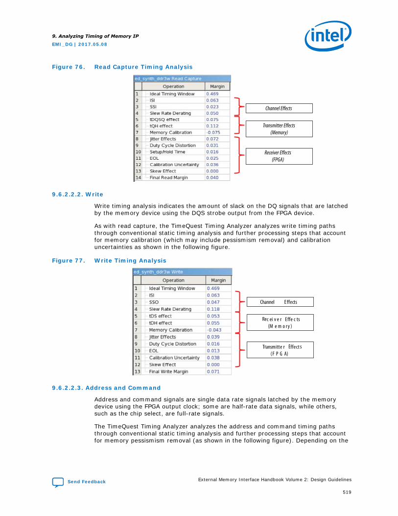
Figure 76. Read Capture Timing Analysis
Channel Effects
Transmitter Effects(Memory)
Receiver Effects(FPGA)
9.6.2.2.2. Write
Write timing analysis indicates the amount of slack on the DQ signals that are latchedby the memory device using the DQS strobe output from the FPGA device.
As with read capture, the TimeQuest Timing Analyzer analyzes write timing pathsthrough conventional static timing analysis and further processing steps that accountfor memory calibration (which may include pessismism removal) and calibrationuncertainties as shown in the following figure.
Figure 77. Write Timing Analysis
Channel E ffects
Rec ei v e r Effe c ts (M e m o r y )
Transmitte r Effect s ( F P G A)
9.6.2.2.3. Address and Command
Address and command signals are single data rate signals latched by the memorydevice using the FPGA output clock; some are half-rate data signals, while others,such as the chip select, are full-rate signals.
The TimeQuest Timing Analyzer analyzes the address and command timing pathsthrough conventional static timing analysis and further processing steps that accountfor memory pessismism removal (as shown in the following figure). Depending on the
9. Analyzing Timing of Memory IP
EMI_DG | 2017.05.08
Send Feedback External Memory Interface Handbook Volume 2: Design Guidelines
519
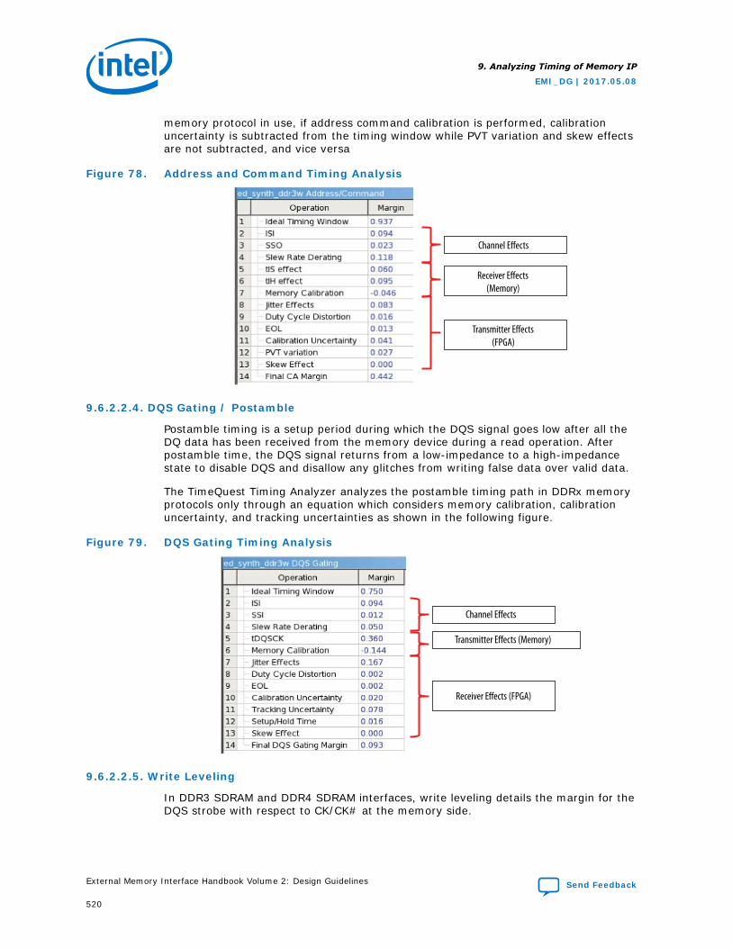
memory protocol in use, if address command calibration is performed, calibrationuncertainty is subtracted from the timing window while PVT variation and skew effectsare not subtracted, and vice versa
Figure 78. Address and Command Timing Analysis
Channel Effects
Receiver Effects(Memory)
Transmitter Effects(FPGA)
9.6.2.2.4. DQS Gating / Postamble
Postamble timing is a setup period during which the DQS signal goes low after all theDQ data has been received from the memory device during a read operation. Afterpostamble time, the DQS signal returns from a low-impedance to a high-impedancestate to disable DQS and disallow any glitches from writing false data over valid data.
The TimeQuest Timing Analyzer analyzes the postamble timing path in DDRx memoryprotocols only through an equation which considers memory calibration, calibrationuncertainty, and tracking uncertainties as shown in the following figure.
Figure 79. DQS Gating Timing Analysis
Channel Effects
Transmitter Effects (Memory)
Receiver Effects (FPGA)
9.6.2.2.5. Write Leveling
In DDR3 SDRAM and DDR4 SDRAM interfaces, write leveling details the margin for theDQS strobe with respect to CK/CK# at the memory side.
9. Analyzing Timing of Memory IP
EMI_DG | 2017.05.08
External Memory Interface Handbook Volume 2: Design Guidelines Send Feedback
520
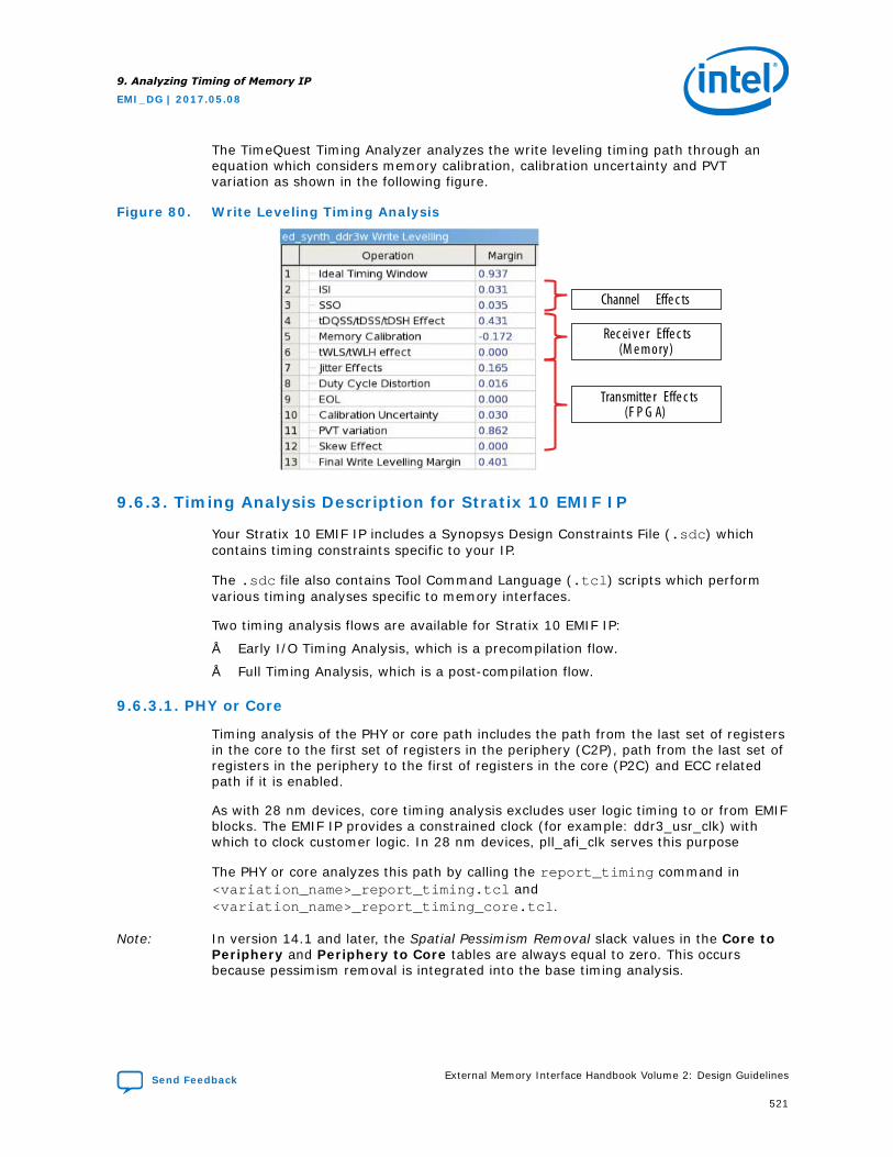
The TimeQuest Timing Analyzer analyzes the write leveling timing path through anequation which considers memory calibration, calibration uncertainty and PVTvariation as shown in the following figure.
Figure 80. Write Leveling Timing Analysis
Channel Effe c ts
Rec ei ve r Effe c ts (M e mo ry)
Transmitte r Effe c ts (F P G A)
9.6.3. Timing Analysis Description for Stratix 10 EMIF IP
Your Stratix 10 EMIF IP includes a Synopsys Design Constraints File (.sdc) whichcontains timing constraints specific to your IP.
The .sdc file also contains Tool Command Language (.tcl) scripts which performvarious timing analyses specific to memory interfaces.
Two timing analysis flows are available for Stratix 10 EMIF IP:
• Early I/O Timing Analysis, which is a precompilation flow.
• Full Timing Analysis, which is a post-compilation flow.
9.6.3.1. PHY or Core
Timing analysis of the PHY or core path includes the path from the last set of registersin the core to the first set of registers in the periphery (C2P), path from the last set ofregisters in the periphery to the first of registers in the core (P2C) and ECC relatedpath if it is enabled.
As with 28 nm devices, core timing analysis excludes user logic timing to or from EMIFblocks. The EMIF IP provides a constrained clock (for example: ddr3_usr_clk) withwhich to clock customer logic. In 28 nm devices, pll_afi_clk serves this purpose
The PHY or core analyzes this path by calling the report_timing command in<variation_name>_report_timing.tcl and<variation_name>_report_timing_core.tcl.
Note: In version 14.1 and later, the Spatial Pessimism Removal slack values in the Core toPeriphery and Periphery to Core tables are always equal to zero. This occursbecause pessimism removal is integrated into the base timing analysis.
9. Analyzing Timing of Memory IP
EMI_DG | 2017.05.08
Send Feedback External Memory Interface Handbook Volume 2: Design Guidelines
521
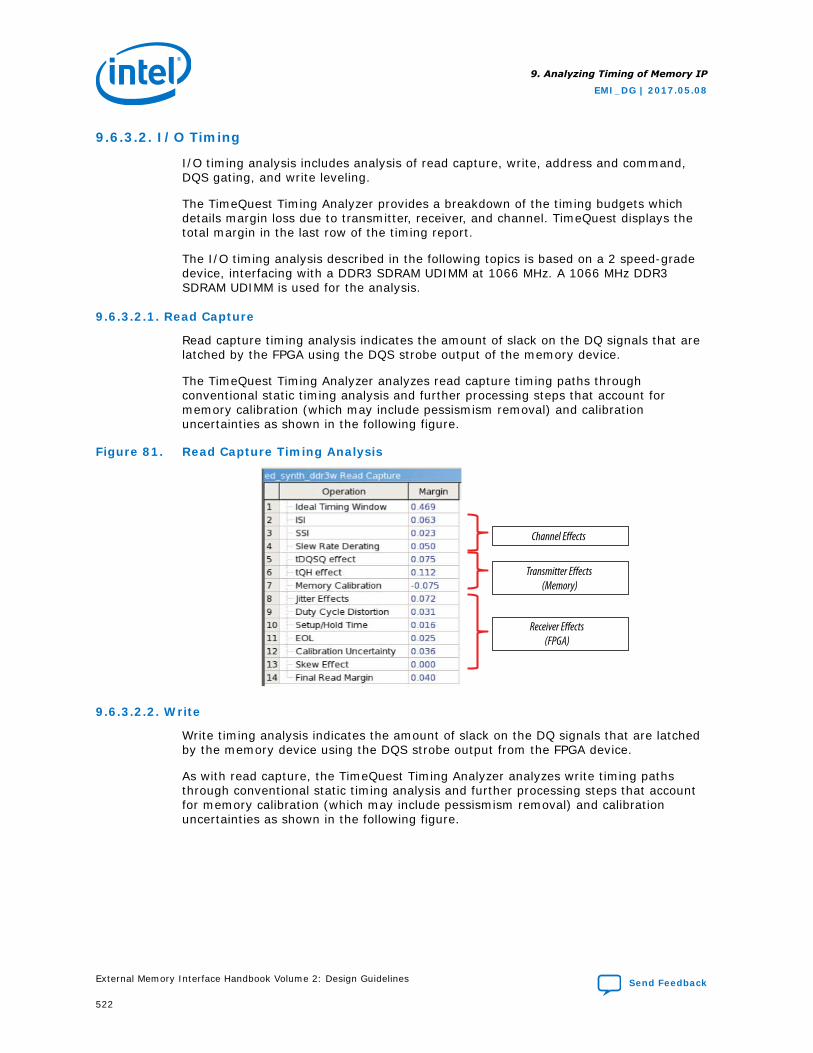
9.6.3.2. I/O Timing
I/O timing analysis includes analysis of read capture, write, address and command,DQS gating, and write leveling.
The TimeQuest Timing Analyzer provides a breakdown of the timing budgets whichdetails margin loss due to transmitter, receiver, and channel. TimeQuest displays thetotal margin in the last row of the timing report.
The I/O timing analysis described in the following topics is based on a 2 speed-gradedevice, interfacing with a DDR3 SDRAM UDIMM at 1066 MHz. A 1066 MHz DDR3SDRAM UDIMM is used for the analysis.
9.6.3.2.1. Read Capture
Read capture timing analysis indicates the amount of slack on the DQ signals that arelatched by the FPGA using the DQS strobe output of the memory device.
The TimeQuest Timing Analyzer analyzes read capture timing paths throughconventional static timing analysis and further processing steps that account formemory calibration (which may include pessismism removal) and calibrationuncertainties as shown in the following figure.
Figure 81. Read Capture Timing Analysis
Channel Effects
Transmitter Effects(Memory)
Receiver Effects(FPGA)
9.6.3.2.2. Write
Write timing analysis indicates the amount of slack on the DQ signals that are latchedby the memory device using the DQS strobe output from the FPGA device.
As with read capture, the TimeQuest Timing Analyzer analyzes write timing pathsthrough conventional static timing analysis and further processing steps that accountfor memory calibration (which may include pessismism removal) and calibrationuncertainties as shown in the following figure.
9. Analyzing Timing of Memory IP
EMI_DG | 2017.05.08
External Memory Interface Handbook Volume 2: Design Guidelines Send Feedback
522
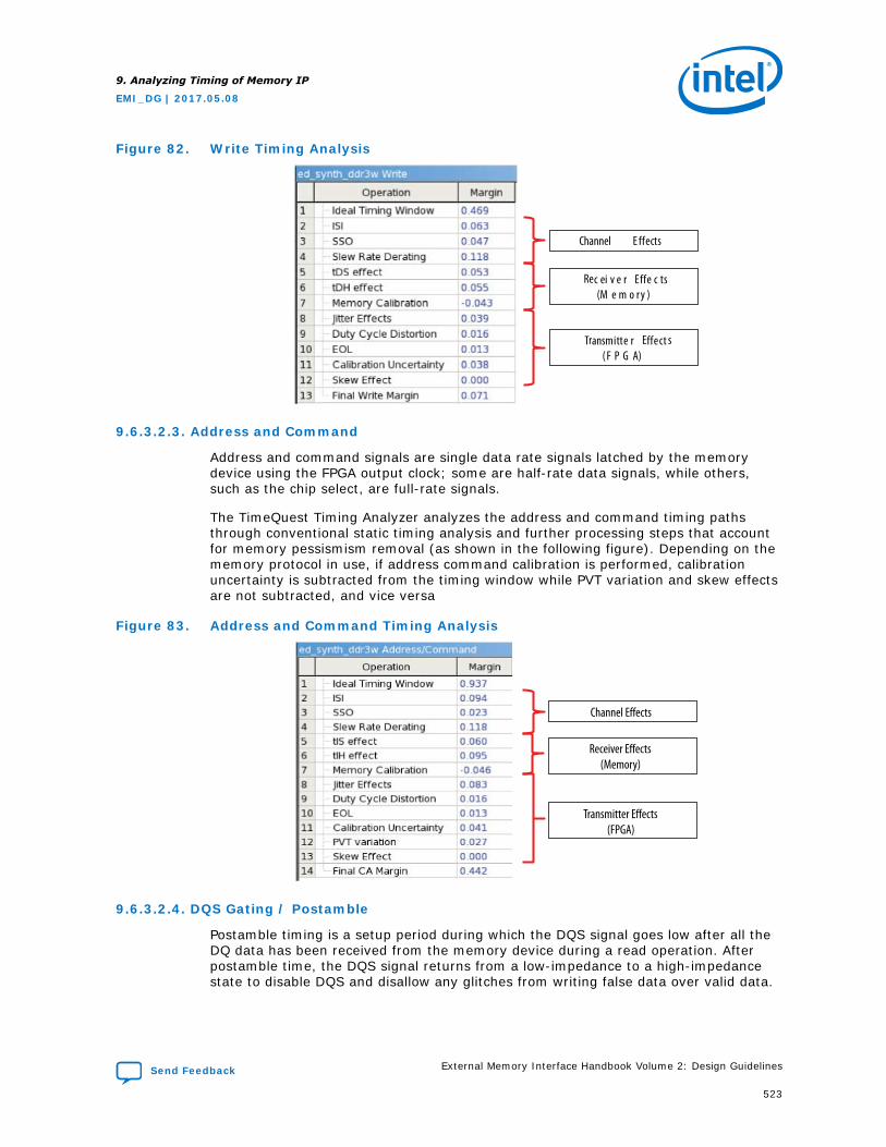
Figure 82. Write Timing Analysis
Channel E ffects
Rec ei v e r Effe c ts (M e m o r y )
Transmitte r Effect s ( F P G A)
9.6.3.2.3. Address and Command
Address and command signals are single data rate signals latched by the memorydevice using the FPGA output clock; some are half-rate data signals, while others,such as the chip select, are full-rate signals.
The TimeQuest Timing Analyzer analyzes the address and command timing pathsthrough conventional static timing analysis and further processing steps that accountfor memory pessismism removal (as shown in the following figure). Depending on thememory protocol in use, if address command calibration is performed, calibrationuncertainty is subtracted from the timing window while PVT variation and skew effectsare not subtracted, and vice versa
Figure 83. Address and Command Timing Analysis
Channel Effects
Receiver Effects(Memory)
Transmitter Effects(FPGA)
9.6.3.2.4. DQS Gating / Postamble
Postamble timing is a setup period during which the DQS signal goes low after all theDQ data has been received from the memory device during a read operation. Afterpostamble time, the DQS signal returns from a low-impedance to a high-impedancestate to disable DQS and disallow any glitches from writing false data over valid data.
9. Analyzing Timing of Memory IP
EMI_DG | 2017.05.08
Send Feedback External Memory Interface Handbook Volume 2: Design Guidelines
523
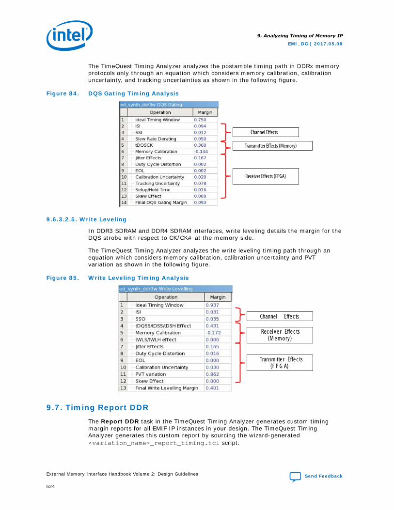
The TimeQuest Timing Analyzer analyzes the postamble timing path in DDRx memoryprotocols only through an equation which considers memory calibration, calibrationuncertainty, and tracking uncertainties as shown in the following figure.
Figure 84. DQS Gating Timing Analysis
Channel Effects
Transmitter Effects (Memory)
Receiver Effects (FPGA)
9.6.3.2.5. Write Leveling
In DDR3 SDRAM and DDR4 SDRAM interfaces, write leveling details the margin for theDQS strobe with respect to CK/CK# at the memory side.
The TimeQuest Timing Analyzer analyzes the write leveling timing path through anequation which considers memory calibration, calibration uncertainty and PVTvariation as shown in the following figure.
Figure 85. Write Leveling Timing Analysis
Channel Effe c ts
Rec ei ve r Effe c ts (M e mo ry)
Transmitte r Effe c ts (F P G A)
9.7. Timing Report DDR
The Report DDR task in the TimeQuest Timing Analyzer generates custom timingmargin reports for all EMIF IP instances in your design. The TimeQuest TimingAnalyzer generates this custom report by sourcing the wizard-generated<variation_name>_report_timing.tcl script.
9. Analyzing Timing of Memory IP
EMI_DG | 2017.05.08
External Memory Interface Handbook Volume 2: Design Guidelines Send Feedback
524
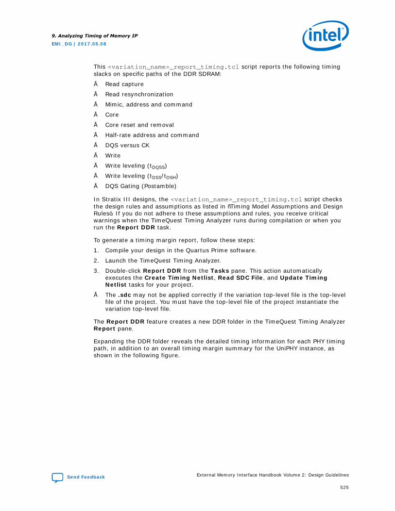
This <variation_name>_report_timing.tcl script reports the following timingslacks on specific paths of the DDR SDRAM:
• Read capture
• Read resynchronization
• Mimic, address and command
• Core
• Core reset and removal
• Half-rate address and command
• DQS versus CK
• Write
• Write leveling (tDQSS)
• Write leveling (tDSS/tDSH)
• DQS Gating (Postamble)
In Stratix III designs, the <variation_name>_report_timing.tcl script checksthe design rules and assumptions as listed in “Timing Model Assumptions and DesignRules”. If you do not adhere to these assumptions and rules, you receive criticalwarnings when the TimeQuest Timing Analyzer runs during compilation or when yourun the Report DDR task.
To generate a timing margin report, follow these steps:
1. Compile your design in the Quartus Prime software.
2. Launch the TimeQuest Timing Analyzer.
3. Double-click Report DDR from the Tasks pane. This action automaticallyexecutes the Create Timing Netlist, Read SDC File, and Update TimingNetlist tasks for your project.
• The .sdc may not be applied correctly if the variation top-level file is the top-levelfile of the project. You must have the top-level file of the project instantiate thevariation top-level file.
The Report DDR feature creates a new DDR folder in the TimeQuest Timing AnalyzerReport pane.
Expanding the DDR folder reveals the detailed timing information for each PHY timingpath, in addition to an overall timing margin summary for the UniPHY instance, asshown in the following figure.
9. Analyzing Timing of Memory IP
EMI_DG | 2017.05.08
Send Feedback External Memory Interface Handbook Volume 2: Design Guidelines
525
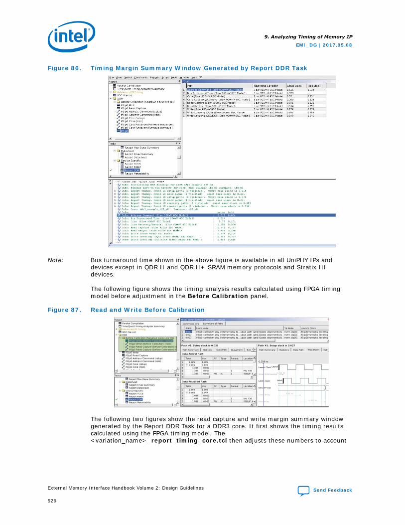
Figure 86. Timing Margin Summary Window Generated by Report DDR Task
Note: Bus turnaround time shown in the above figure is available in all UniPHY IPs anddevices except in QDR II and QDR II+ SRAM memory protocols and Stratix IIIdevices.
The following figure shows the timing analysis results calculated using FPGA timingmodel before adjustment in the Before Calibration panel.
Figure 87. Read and Write Before Calibration
The following two figures show the read capture and write margin summary windowgenerated by the Report DDR Task for a DDR3 core. It first shows the timing resultscalculated using the FPGA timing model. The<variation_name>_report_timing_core.tcl then adjusts these numbers to account
9. Analyzing Timing of Memory IP
EMI_DG | 2017.05.08
External Memory Interface Handbook Volume 2: Design Guidelines Send Feedback
526
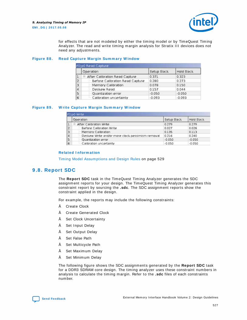
for effects that are not modeled by either the timing model or by TimeQuest TimingAnalyzer. The read and write timing margin analysis for Stratix III devices does notneed any adjustments.
Figure 88. Read Capture Margin Summary Window
Figure 89. Write Capture Margin Summary Window
Related Information
Timing Model Assumptions and Design Rules on page 529
9.8. Report SDC
The Report SDC task in the TimeQuest Timing Analyzer generates the SDCassignment reports for your design. The TimeQuest Timing Analyzer generates thisconstraint report by sourcing the .sdc. The SDC assignment reports show theconstraint applied in the design.
For example, the reports may include the following constraints:
• Create Clock
• Create Generated Clock
• Set Clock Uncertainty
• Set Input Delay
• Set Output Delay
• Set False Path
• Set Multicycle Path
• Set Maximum Delay
• Set Minimum Delay
The following figure shows the SDC assignments generated by the Report SDC taskfor a DDR3 SDRAM core design. The timing analyzer uses these constraint numbers inanalysis to calculate the timing margin. Refer to the .sdc files of each constraintsnumber.
9. Analyzing Timing of Memory IP
EMI_DG | 2017.05.08
Send Feedback External Memory Interface Handbook Volume 2: Design Guidelines
527
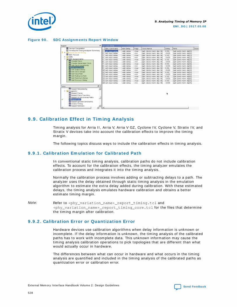
Figure 90. SDC Assignments Report Window
9.9. Calibration Effect in Timing Analysis
Timing analysis for Arria II, Arria V, Arria V GZ, Cyclone IV, Cyclone V, Stratix IV, andStratix V devices take into account the calibration effects to improve the timingmargin.
The following topics discuss ways to include the calibration effects in timing analysis.
9.9.1. Calibration Emulation for Calibrated Path
In conventional static timing analysis, calibration paths do not include calibrationeffects. To account for the calibration effects, the timing analyzer emulates thecalibration process and integrates it into the timing analysis.
Normally the calibration process involves adding or subtracting delays to a path. Theanalyzer uses the delay obtained through static timing analysis in the emulationalgorithm to estimate the extra delay added during calibration. With these estimateddelays, the timing analysis emulates hardware calibration and obtains a betterestimate timing margin.
Note: Refer to <phy_variation_name>_report_timing.tcl and<phy_variation_name>_report_timing_core.tcl for the files that determinethe timing margin after calibration.
9.9.2. Calibration Error or Quantization Error
Hardware devices use calibration algorithms when delay information is unknown orincomplete. If the delay information is unknown, the timing analysis of the calibratedpaths has to work with incomplete data. This unknown information may cause thetiming analysis calibration operations to pick topologies that are different than whatwould actually occur in hardware.
The differences between what can occur in hardware and what occurs in the timinganalysis are quantified and included in the timing analysis of the calibrated paths asquantization error or calibration error.
9. Analyzing Timing of Memory IP
EMI_DG | 2017.05.08
External Memory Interface Handbook Volume 2: Design Guidelines Send Feedback
528
9.9.3. Calibration Uncertainties
Calibration results may change or reduce due to one or more of the followinguncertainties:
• Jitter and duty cycle distortion (DCD) effects
• Voltage and temperature variations
• Board trace delays changing due to noise on terminated supply voltages
These calibration uncertainties are accounted for in the timing analysis.
9.9.4. Memory Calibration
All the timing paths reported include one or more memory parameters, such as tDQSSand tDQSQ. These specifications indicate the amount of variation that occurs in varioustiming paths in the memory and abstracts them into singular values so that they canbe used by others when interfacing with the memory device.
JEDEC defines these parameters in their specification for memory standards, andevery memory vendor must meet this specification or improve it. However, there is noproportion of each specification due to different types of variations. Variations that areof interest are typically grouped into three different types: process variations (P),voltage variations (V), and temperature variations (T). These together compose PVTvariations that typically define the JEDEC specification. You can determine themaximum P variation by comparing different dies, and you can determine themaximum V and T variations by operating a design at the endpoints of the range ofvoltage and temperature. P variations do not change once the chip has beenfabricated, while V and T variations change over time.
The timing analysis for Stratix V FPGAs at 667 MHz of various paths (if the analysis iscomprehensive and includes all the sources of noise) indicate that there is no timingmargin available. However, the designs do actually work in practice with a reasonableamount of margin. The reason for this behavior is that the memory devices typicallyhave specifications that easily beat the JEDEC specification and that our calibrationalgorithms calibrate out the process portion of the JEDEC specification, leaving onlythe V and T portions of the variations.
The memory calibration figure determination includes noting what percentage of theJEDEC specification of various memory parameters is caused by process variations forwhich UniPHY calibration algorithms can calibrate out, and to apply that to the fullJEDEC specification. The remaining portion of the variation is caused by voltage andtemperature variations which cannot be calibrated out.
You can find the percentage of the JEDEC specification that is due to process variationis set in <variation_name>_report_timing.tcl .
9.10. Timing Model Assumptions and Design Rules
External memory interfaces using Intel FPGA IP are optimized for highestperformance, and use a high-performance timing model to analyze calibrated andsource-synchronous, double-data rate I/O timing paths. This timing model applies todesigns that adhere to a set of predefined assumptions.
9. Analyzing Timing of Memory IP
EMI_DG | 2017.05.08
Send Feedback External Memory Interface Handbook Volume 2: Design Guidelines
529
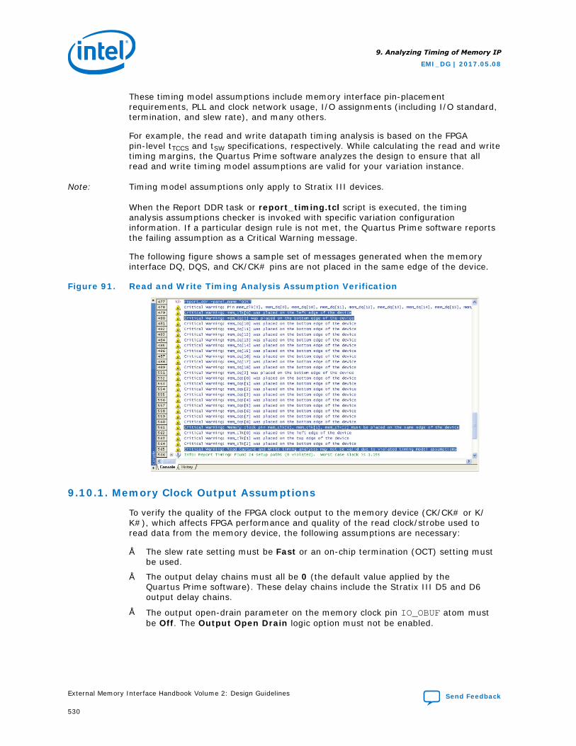
These timing model assumptions include memory interface pin-placementrequirements, PLL and clock network usage, I/O assignments (including I/O standard,termination, and slew rate), and many others.
For example, the read and write datapath timing analysis is based on the FPGApin-level tTCCS and tSW specifications, respectively. While calculating the read and writetiming margins, the Quartus Prime software analyzes the design to ensure that allread and write timing model assumptions are valid for your variation instance.
Note: Timing model assumptions only apply to Stratix III devices.
When the Report DDR task or report_timing.tcl script is executed, the timinganalysis assumptions checker is invoked with specific variation configurationinformation. If a particular design rule is not met, the Quartus Prime software reportsthe failing assumption as a Critical Warning message.
The following figure shows a sample set of messages generated when the memoryinterface DQ, DQS, and CK/CK# pins are not placed in the same edge of the device.
Figure 91. Read and Write Timing Analysis Assumption Verification
9.10.1. Memory Clock Output Assumptions
To verify the quality of the FPGA clock output to the memory device (CK/CK# or K/K#), which affects FPGA performance and quality of the read clock/strobe used toread data from the memory device, the following assumptions are necessary:
• The slew rate setting must be Fast or an on-chip termination (OCT) setting mustbe used.
• The output delay chains must all be 0 (the default value applied by theQuartus Prime software). These delay chains include the Stratix III D5 and D6output delay chains.
• The output open-drain parameter on the memory clock pin IO_OBUF atom mustbe Off. The Output Open Drain logic option must not be enabled.
9. Analyzing Timing of Memory IP
EMI_DG | 2017.05.08
External Memory Interface Handbook Volume 2: Design Guidelines Send Feedback
530
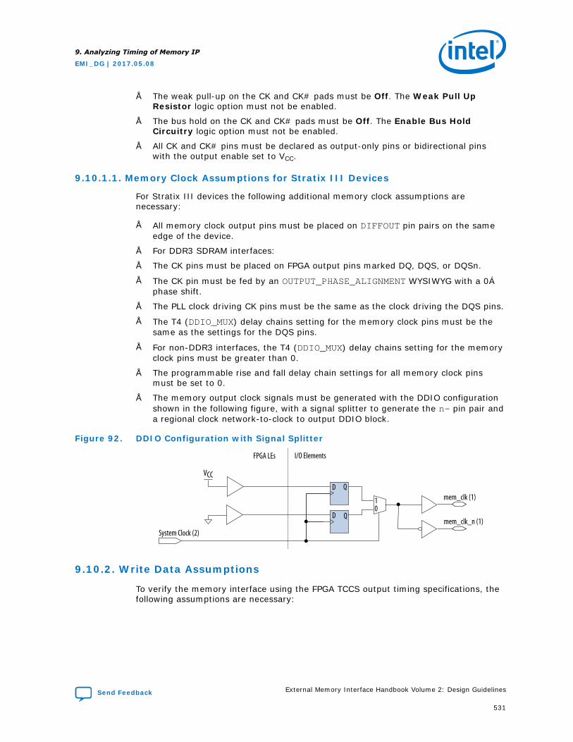
• The weak pull-up on the CK and CK# pads must be Off. The Weak Pull UpResistor logic option must not be enabled.
• The bus hold on the CK and CK# pads must be Off. The Enable Bus HoldCircuitry logic option must not be enabled.
• All CK and CK# pins must be declared as output-only pins or bidirectional pinswith the output enable set to VCC.
9.10.1.1. Memory Clock Assumptions for Stratix III Devices
For Stratix III devices the following additional memory clock assumptions arenecessary:
• All memory clock output pins must be placed on DIFFOUT pin pairs on the sameedge of the device.
• For DDR3 SDRAM interfaces:
• The CK pins must be placed on FPGA output pins marked DQ, DQS, or DQSn.
• The CK pin must be fed by an OUTPUT_PHASE_ALIGNMENT WYSIWYG with a 0°phase shift.
• The PLL clock driving CK pins must be the same as the clock driving the DQS pins.
• The T4 (DDIO_MUX) delay chains setting for the memory clock pins must be thesame as the settings for the DQS pins.
• For non-DDR3 interfaces, the T4 (DDIO_MUX) delay chains setting for the memoryclock pins must be greater than 0.
• The programmable rise and fall delay chain settings for all memory clock pinsmust be set to 0.
• The memory output clock signals must be generated with the DDIO configurationshown in the following figure, with a signal splitter to generate the n- pin pair anda regional clock network-to-clock to output DDIO block.
Figure 92. DDIO Configuration with Signal Splitter
mem_clk (1)QD
QD
System Clock (2)
FPGA LEs I/O Elements
VCC
mem_clk_n (1)
10
9.10.2. Write Data Assumptions
To verify the memory interface using the FPGA TCCS output timing specifications, thefollowing assumptions are necessary:
9. Analyzing Timing of Memory IP
EMI_DG | 2017.05.08
Send Feedback External Memory Interface Handbook Volume 2: Design Guidelines
531
• For QDRII and QDRII+ memory interfaces, the write clock output pins (such asK/K# or DK/DK#) must be placed in DQS/DQSn pin pairs.
• The PLL clock used to generate the write-clock signals and the PLL clock used togenerate the write-data signals must come from the same PLL.
• The slew rate for all write clocks and write data pins must be set to Fast or OCTmust be used.
• When auto deskew is not enabled, the output delay chains and output enabledelay chains must all be set to the default values applied by the Quartus Primesoftware. These delay chains include the Stratix III D5 and D6 delay chains.
• The output open drain for all write clocks and write data pins’ IO_OBUF atom mustbe set to Off. The Output Open Drain logic option must not be enabled.
• The weak pull-up for all write clocks and write data pins must be set to Off. TheWeak Pull Up Resistor logic option must not be enabled.
• The Bus Hold for all write clocks and write data pins must be set to Off. TheEnable Bus Hold Circuitry logic option must not be enabled.
9.10.2.1. Write Data Assumptions for Stratix III Devices
For Stratix III devices the following additional write data assumptions are necessary:
• Differential write clock signals (DQS/DQSn) must be generated using the signalsplitter.
• The write data pins (including the DM pins) must be placed in related DQ pinsassociated with the chosen DQS pin. The only exception to this rule is for QDRIIand QDRII+ ×36 interfaces emulated using two ×18 DQ groups. For suchinterfaces, all of the write data pins must be placed on the same edge of thedevice (left, right, top, or bottom). Also, the write clock K/K# pin pair should beplaced on one of the DQS/DQSn pin pairs on the same edge.
• All write clock pins must have similar circuit structure.
— For DDR2 SDRAM interfaces and DDR3 SDRAM with leveling interfaces, allDQS/DQS# write strobes must be fed by DDIO output registers clocked by thewrite-leveling delay chain in the OUTPUT_PHASE_ALIGNMENT block.
— For DDR and DDR2 SDRAM interfaces, all write clock pins must be fed byDDIO output registers clocked by a global or regional clock network.
• All write data pins must have similar circuit structure.
— For DDR3 SDRAM interfaces, all write data pins must be fed by either DDIOoutput registers clocked by the OUTPUT_PHASE_ALIGNMENT block, VCC, orGND.
— For DDR and DDR2 SDRAM interfaces, all write data pins must be fed by eitherDDIO output registers clocked by a global or regional clock network, VCC, orGND.
9. Analyzing Timing of Memory IP
EMI_DG | 2017.05.08
External Memory Interface Handbook Volume 2: Design Guidelines Send Feedback
532
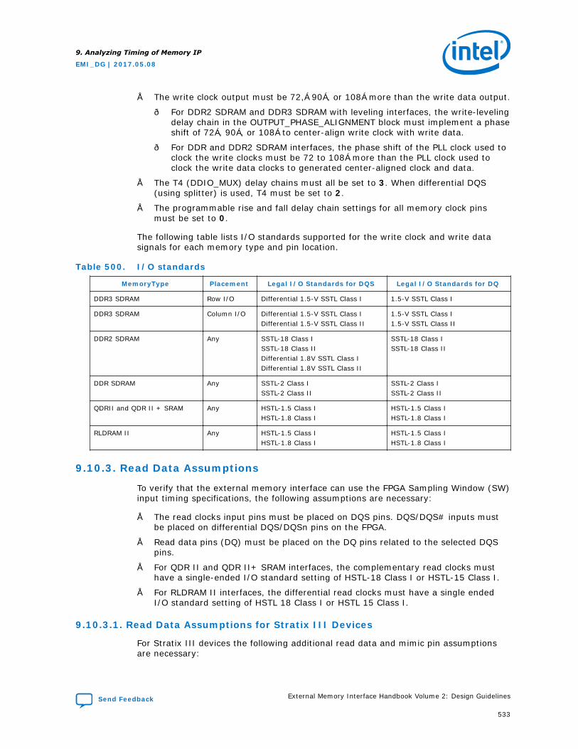
• The write clock output must be 72,° 90°, or 108° more than the write data output.
— For DDR2 SDRAM and DDR3 SDRAM with leveling interfaces, the write-levelingdelay chain in the OUTPUT_PHASE_ALIGNMENT block must implement a phaseshift of 72°, 90°, or 108° to center-align write clock with write data.
— For DDR and DDR2 SDRAM interfaces, the phase shift of the PLL clock used toclock the write clocks must be 72 to 108° more than the PLL clock used toclock the write data clocks to generated center-aligned clock and data.
• The T4 (DDIO_MUX) delay chains must all be set to 3. When differential DQS(using splitter) is used, T4 must be set to 2.
• The programmable rise and fall delay chain settings for all memory clock pinsmust be set to 0.
The following table lists I/O standards supported for the write clock and write datasignals for each memory type and pin location.
Table 500. I/O standards
MemoryType Placement Legal I/O Standards for DQS Legal I/O Standards for DQ
DDR3 SDRAM Row I/O Differential 1.5-V SSTL Class I 1.5-V SSTL Class I
DDR3 SDRAM Column I/O Differential 1.5-V SSTL Class IDifferential 1.5-V SSTL Class II
1.5-V SSTL Class I1.5-V SSTL Class II
DDR2 SDRAM Any SSTL-18 Class ISSTL-18 Class IIDifferential 1.8V SSTL Class IDifferential 1.8V SSTL Class II
SSTL-18 Class ISSTL-18 Class II
DDR SDRAM Any SSTL-2 Class ISSTL-2 Class II
SSTL-2 Class ISSTL-2 Class II
QDRII and QDR II + SRAM Any HSTL-1.5 Class IHSTL-1.8 Class I
HSTL-1.5 Class IHSTL-1.8 Class I
RLDRAM II Any HSTL-1.5 Class IHSTL-1.8 Class I
HSTL-1.5 Class IHSTL-1.8 Class I
9.10.3. Read Data Assumptions
To verify that the external memory interface can use the FPGA Sampling Window (SW)input timing specifications, the following assumptions are necessary:
• The read clocks input pins must be placed on DQS pins. DQS/DQS# inputs mustbe placed on differential DQS/DQSn pins on the FPGA.
• Read data pins (DQ) must be placed on the DQ pins related to the selected DQSpins.
• For QDR II and QDR II+ SRAM interfaces, the complementary read clocks musthave a single-ended I/O standard setting of HSTL-18 Class I or HSTL-15 Class I.
• For RLDRAM II interfaces, the differential read clocks must have a single endedI/O standard setting of HSTL 18 Class I or HSTL 15 Class I.
9.10.3.1. Read Data Assumptions for Stratix III Devices
For Stratix III devices the following additional read data and mimic pin assumptionsare necessary:
9. Analyzing Timing of Memory IP
EMI_DG | 2017.05.08
Send Feedback External Memory Interface Handbook Volume 2: Design Guidelines
533
• For DDR3, DDR2, and DDR SDRAM interfaces, the read clock pin can only drive aDQS bus clocking a ×4 or ×9 DQ group.
• For QDR II, QDR II+ SRAM, and RLDRAM II interfaces, the read clock pin can onlydrive a DQS bus clocking a ×9, ×18, or ×36 DQ group.
• For non-wraparound DDR, DDR2, and DDR3 interfaces, the mimic pin, all readclock, and all read data pins must be placed on the same edge of the device (top,bottom, left, or right). For wraparound interfaces, these pins can be placed onadjacent row I/O and column I/O edges and operate at reduced frequencies.
• All read data pins and the mimic pin must feed DDIO_IN registers and their inputdelay chains D1, D2, and D3 set to default values.
• DQS phase-shift setting must be either 72° or 90° (supports only one phase shiftfor each operating band and memory standard).
• All read clock pins must have the dqs_ctrl_latches_enable parameter of itsDQS_DELAY_CHAIN WYSIWYG set to false.
• The read clocks pins must have their D4 delay chain set to the Quartus Primesoftware default value of 0.
• The read data pins must have their T8 delay chain set to the Quartus Primesoftware default value of 0.
• When differential DQS strobes are used (DDR3 and DDR2 SDRAM), the mimic pinmust feed a true differential input buffer. Placing the memory clock pin on aDIFFIO_RX pin pair allows the mimic path to track timing variations on the DQSinput path.
• When single ended DQS strobes are used, the mimic pin must feed a single endedinput buffer.
9.10.4. DLL Assumptions
The following DLL assumptions are necessary:
• The DLL must directly feed its delayctrlout[] outputs to all DQS pins withoutintervening logic or inversions.
• The DLL must be in a valid frequency band of operation as defined in thecorresponding device data sheet.
• The DLL must have jitter reduction mode and dual-phase comparators enabled.
9.10.5. PLL and Clock Network Assumptions for Stratix III Devices
To verify that the memory interface’s PLL is configured correctly, the followingassumptions are necessary:
9. Analyzing Timing of Memory IP
EMI_DG | 2017.05.08
External Memory Interface Handbook Volume 2: Design Guidelines Send Feedback
534
• The PLL that generates the memory output clock signals and write data and clocksignals must be set to No compensation mode to minimize output clock jitter.
• The reference input clock signal to the PLL must be driven by the dedicated clockinput pin located adjacent to the PLL, or from the clock output signal from theadjacent PLL. If the reference clock cascades from another PLL, that upstream PLLmust be in No compensation mode and Low bandwidth mode.
• For DDR3 and DDR2 SDRAM interfaces, use only regional or dual regional clocknetworks to route PLL outputs that generate the write data, write clock, andmemory output clock signals. This requirement ensures that the memory outputclocks (CK/CK#) meet the memory device input clock jitter specifications, and thatoutput timing variations or skews are minimized.
• For other memory types, the same clock tree type (global, regional, or dualregional) is recommended for PLL clocks generating the write clock, write data,and memory clock signals to minimize timing variations or skew between theseoutputs.
9.11. Common Timing Closure Issues
The following topics describe potential timing closure issues that can occur when usingthe UniPHY IP.
For possible timing closure issues with UniPHY variations, refer to the Quartus PrimeSoftware Release Notes for the software version that you are using. You can solvesome timing issues by moving registers or changing the project fitting setting toStandard (from Auto).
The Quartus Prime Software Release Notes list common timing issues that can beencountered in a particular version of the Quartus Prime software.
Note: In UniPHY-based memory controllers, the derive_pll_clocks command can affecttiming closure if it is called before the memory controller files are loaded. Ensure thatthe Quartus Prime IP File (.qip) appears in the file list before any Synopsys DesignConstraint Files (.sdc) files that contain derive_pll_clocks.
Related Information
Quartus Prime Software and Device Support Release Notes
9.11.1. Missing Timing Margin Report
The UniPHY timing margin reports may not be generated during compilation if the .sdcdoes not appear in the Quartus Prime project settings.
Timing margin reports are not generated if you specify the UniPHY variation as thetop-level project entity. Instantiate the UniPHY variation as a lower level module inyour user design or memory controller.
9.11.2. Incomplete Timing Margin Report
The timing report may not include margin information for certain timing paths ifcertain memory interface pins are optimized away during synthesis.
9. Analyzing Timing of Memory IP
EMI_DG | 2017.05.08
Send Feedback External Memory Interface Handbook Volume 2: Design Guidelines
535

Verify that all memory interface pins appear in the <variation>_all_pins.txt filegenerated during compilation, and ensure that they connect to the I/O pins of thetop-level FPGA design.
9.11.3. Read Capture Timing
In Stratix III and Stratix IV devices, read capture timing may fail if the DQS phaseshift selected is not optimal or if the board skew specified is large.
• You can adjust the effective DQS phase shift implemented by the DLL to balancesetup and hold margins on the read timing path. The DQS phase shift can beadjusted in coarse PVT-compensated steps of 22.5°, 30°, 36°, or 45° by changingthe number of delay buffers (range 1 to 4), or in fine steps using the DQS phaseoffset feature that supports uncompensated delay addition and subtraction inapproximately 12 ps steps.
• To adjust the coarse phase shift selection, determine the supported DLL modes foryour chosen memory interface frequency by referencing the DLL and DQS LogicBlock Specifications tables in the Switching Characteristics section of the devicedata sheet. For example, a 400 MHz DDR2 interface on a -2 speed grade devicecan use DLL mode 5 (resolution 36°, range 290 – 450 MHz) to implement a 72°phase shift, or DLL mode 6 (resolution 45°, range 360–560 MHz) to implement a90° phase shift.
Note: Ensure that you specify the appropriate board-skew parameter when you parameterizethe controllers in the parameter editor. The default board trace length mismatch usedis 20 ps.
9.11.4. Write Timing
Negative timing margins may be reported for write timing paths if the PLL phase shiftused to generate the write data signals is not optimal.
Adjust the PLL phase shift selection on the write clock PLL output using the PLLparameter editor.
Note: Regenerating the UniPHY-based controller overwrites changes made using the PLLparameter editor.
9.11.5. Address and Command Timing
You can optimize the timing margins on the address and command timing path bychanging the PLL phase shift used to generate these signals. In the DDR2 or DDR3SDRAM Controllers with UniPHY IP cores, modify the Additional CK/CK# phase andAdditional Address and Command clock phase parameters.
The DDR2 and DDR3 SDRAM memory controllers use 1T memory timing even in half-rate mode, which may affect the address command margins for DDR2 or DDR3SDRAM designs that use memory DIMMs. DDR2 SDRAM designs have a greater impactbecause the address command bus fans out to all the memory devices on a DIMMincreasing the loading effect on the bus. Make sure your board designs are robustenough to have the memory clock rising edge within the 1T address commandwindow. You can also use the Additional Address and Command clock phaseparameter to adjust the phase of the address and command if needed.
9. Analyzing Timing of Memory IP
EMI_DG | 2017.05.08
External Memory Interface Handbook Volume 2: Design Guidelines Send Feedback
536
The far-end load value and board trace delay differences between address andcommand and memory clock pins can result in timing failures if they are notaccounted for during timing analysis.
The Quartus Prime Fitter may not optimally set output delay chains on the addressand command pins. To ensure that any PLL phase-shift adjustments are not negatedby delay chain adjustments, create logic assignments using the Assignment Editor toset all address and command output pin D5 delay chains to 0.
For Stratix III and Stratix IV devices, some corner cases of device family and memoryfrequency may require an increase to the address and command clock phase to meetcore timing. You can identify this situation, if the DDR timing report shows a PHYsetup violation with the phy_clk launch clock, and the address and command latchclock—clock 0 (half-rate phy_clk) or 2 (full-rate phy_clk), and 6, respectively.
If you see this timing violation, you may fix it by advancing the address and commandclock phase as required. For example, a 200-ps violation for a 400-MHz interfacerepresents 8% of the clock period, or 28.8. Therefore, advance the address andcommand phase from 270 to 300. However, this action reduces the setup and holdmargin at the DDR device.
9.11.6. PHY Reset Recovery and Removal
A common cause for reset timing violations in UniPHY designs is the selection of aglobal or regional clock network for a reset signal.
The UniPHY IP does not require any dedicated clock networks for reset signals. OnlyUniPHY PLL outputs require clock networks, and any other PHY signal using clocknetworks may result in timing violations.
You can correct such timing violations by:
• Setting the Global Signal logic assignment to Off for the problem path (using theAssignment Editor), or
• Adjusting the logic placement (using the Assignment Editor or Chip Planner)
9.11.7. Clock-to-Strobe (for DDR and DDR2 SDRAM Only)
Memory output clock signals and DQS strobes are generated using the same PLLoutput clock. Therefore, no timing optimization is possible for this path and positivetiming margins are expected for interfaces running at or below the FPGA data sheetspecifications.
For DDR3 interfaces, the timing margin for this path is reported as Write Leveling.
9.11.8. Read Resynchronization and Write Leveling Timing (for SDRAMOnly)
These timing paths apply only to Arria II GX, Stratix III, and Stratix IV devices, andare implemented using calibrated clock signals driving dedicated IOE registers.Therefore, no timing optimization is possible for these paths, and positive timingmargin is expected for interfaces running at or below the FPGA data sheetspecifications.
9. Analyzing Timing of Memory IP
EMI_DG | 2017.05.08
Send Feedback External Memory Interface Handbook Volume 2: Design Guidelines
537
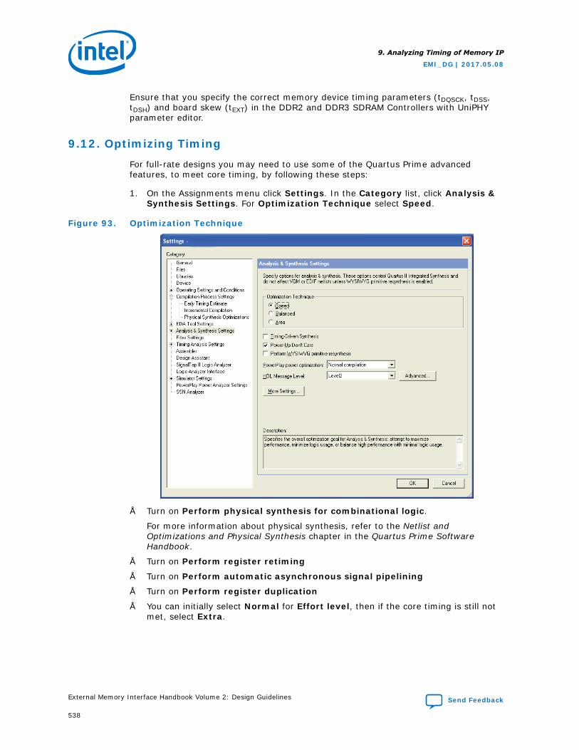
Ensure that you specify the correct memory device timing parameters (tDQSCK, tDSS,tDSH) and board skew (tEXT) in the DDR2 and DDR3 SDRAM Controllers with UniPHYparameter editor.
9.12. Optimizing Timing
For full-rate designs you may need to use some of the Quartus Prime advancedfeatures, to meet core timing, by following these steps:
1. On the Assignments menu click Settings. In the Category list, click Analysis &Synthesis Settings. For Optimization Technique select Speed.
Figure 93. Optimization Technique
• Turn on Perform physical synthesis for combinational logic.
For more information about physical synthesis, refer to the Netlist andOptimizations and Physical Synthesis chapter in the Quartus Prime SoftwareHandbook.
• Turn on Perform register retiming
• Turn on Perform automatic asynchronous signal pipelining
• Turn on Perform register duplication
• You can initially select Normal for Effort level, then if the core timing is still notmet, select Extra.
9. Analyzing Timing of Memory IP
EMI_DG | 2017.05.08
External Memory Interface Handbook Volume 2: Design Guidelines Send Feedback
538
Figure 94. Physical Synthesis Optimizations
Related Information
Netlist Optimizations and Physical Synthesis
9.13. Timing Deration Methodology for Multiple Chip Select DDR2and DDR3 SDRAM Designs
In a multiple chip select system, each individual rank has its own chip select signal.Consequently, you must change the Total Memory chip selects, Number of chipselect (for discrete components) or Number of chip select per slot (DIMMs) in thePreset Editor of the UniPHY-based parameter editors.
In the Preset Editor, you must leave the baseline non-derated tDS, tDH, tIS, tIHvalues, because the settings on the Board Settings page account for multiple chipselect slew rate deration.
The following topics explain two timing deration methodologies for multiple chip-selectDDR2 and DDR3 SDRAM designs:
• Timing Deration using the Board Settings
• Timing Deration Using the Excel-Based Calculator
For Arria II GX, Arria II GZ, Arria V GZ, Cyclone V, Stratix IV, and Stratix V devices,the UniPHY-based controller parameter editor has an option to select multiple chip-select deration.
9. Analyzing Timing of Memory IP
EMI_DG | 2017.05.08
Send Feedback External Memory Interface Handbook Volume 2: Design Guidelines
539
Note: To perform multiple chip-select timing deration for other Intel devices (such as StratixIII devices), Intel provides an Excel-based
Timing deration in this section applies to either discrete components or DIMMs.
Note: You can derate DDR SDRAM multiple chip select designs by using the DDR2 SDRAMsection of the Excel-based calculator, but Intel does not guarantee the results.
This section assumes you know how to obtain data on PCB simulations for timingderation from HyperLynx or any other PCB simulator.
Related Information
• Timing Deration using the Board Settings on page 542
• Multi-Chip Select Calculator
9.13.1. Multiple Chip Select Configuration Effects
A DIMM contains one or several RAM chips on a small PCB with pins that connect it toanother system such as a motherboard or router.
Nonregistered (unbuffered) DIMMs (or UDIMMs) connect address and control busesdirectly from the module interface to the DRAM on the module.
Registered DIMMs (RDIMMs) and load-reduced DIMMs (LRDIMMs) improve signalintegrity (and hence potential clock rates and/or overall memory size) by electricallybuffering address and command signals as well as the data bus (for LRDIMMs) at acost of additional latency. Both RDIMMs and LRDIMMs use parity on the address andcommand bus for increased robustness.
Multiple chip select configurations allow for one set of data pins (and address pins forUDIMMs) to be connected to two or more memory ranks. Multiple chip selectconfigurations have a number of effects on the timing analysis including theintersymbol interference (ISI) effects, board effects, and calibration effects.
9.13.1.1. ISI Effects
With multiple chip selects and possible slots loading the far end of the pin, there maybe ISI effects on a signal causing the eye openings for DQ, DQS, and address andcommand signals to be smaller than for single-rank designs.
The following figure shows the eye shrinkage for DQ signal of a single rank system(top) and multiple chip select system (bottom). The ISI eye reductions reduce thetiming window available for both the write path and the address and command pathanalysis. You must specify them as output delay constraints in the .sdc.
Extra loading from the additional ranks causes the slew rate of signals from the FPGAto be reduced. This reduction in slew rate affects some of the memory parametersincluding data, address, command and control setup and hold times (tDS, tDH, tIS,and tIH).
9. Analyzing Timing of Memory IP
EMI_DG | 2017.05.08
External Memory Interface Handbook Volume 2: Design Guidelines Send Feedback
540
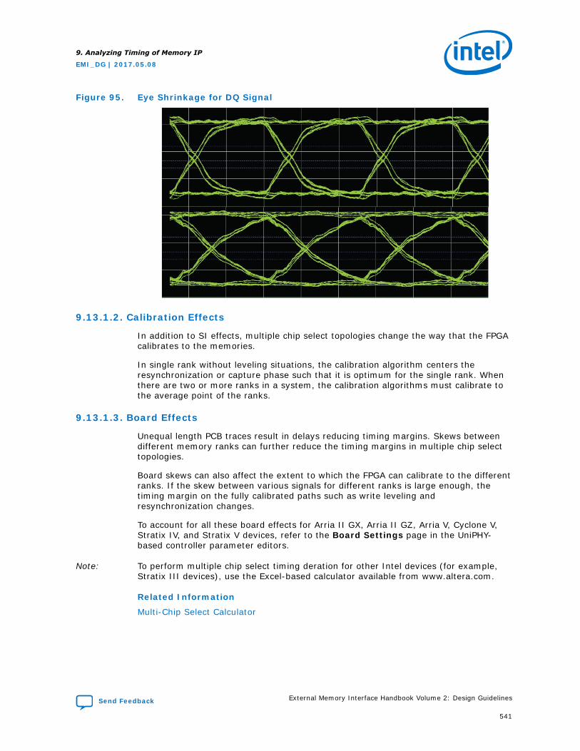
Figure 95. Eye Shrinkage for DQ Signal
9.13.1.2. Calibration Effects
In addition to SI effects, multiple chip select topologies change the way that the FPGAcalibrates to the memories.
In single rank without leveling situations, the calibration algorithm centers theresynchronization or capture phase such that it is optimum for the single rank. Whenthere are two or more ranks in a system, the calibration algorithms must calibrate tothe average point of the ranks.
9.13.1.3. Board Effects
Unequal length PCB traces result in delays reducing timing margins. Skews betweendifferent memory ranks can further reduce the timing margins in multiple chip selecttopologies.
Board skews can also affect the extent to which the FPGA can calibrate to the differentranks. If the skew between various signals for different ranks is large enough, thetiming margin on the fully calibrated paths such as write leveling andresynchronization changes.
To account for all these board effects for Arria II GX, Arria II GZ, Arria V, Cyclone V,Stratix IV, and Stratix V devices, refer to the Board Settings page in the UniPHY-based controller parameter editors.
Note: To perform multiple chip select timing deration for other Intel devices (for example,Stratix III devices), use the Excel-based calculator available from www.altera.com.
Related Information
Multi-Chip Select Calculator
9. Analyzing Timing of Memory IP
EMI_DG | 2017.05.08
Send Feedback External Memory Interface Handbook Volume 2: Design Guidelines
541
9.13.2. Timing Deration using the Board Settings
When you target Arria II GX, Arria II GZ, Arria V, Cyclone V, Stratix IV, or Stratix Vdevices, the UniPHY-based parameter editors include the Board Settings page, toautomatically account for the timing deration caused by the multiple chip selects inyour design.
When you target Stratix III devices, you can derate single chip-select designs usingthe parameter editors to account for the skews, ISI, and slew rates in the BoardSettings page.
If you are targeting Stratix III devices you see the following warning:
"Warning: Calibration performed on all chip selects, timing analysis only performed onfirst chip select. Manual timing derating is required"
Note: You must perform manual timing deration using the Excel-based calculator.
The Board Settings page allows you to enter the parameters related to the boarddesign including skews, signal integrity, and slew rates. The Board Settings pagealso includes the board skew setting parameter, Addr/Command to CK skew.
9.13.2.1. Slew Rates
You can obtain the slew rates in one of the following ways:
• Intel performs PCB simulations on internal Intel boards to compute the outputslew rate and ISI effects of various multiple chip select configurations. Thesesimulation numbers are prepopulated in the Slew Rates based on the number ofranks selected. The address and command setup and hold times (tDS, tDH, tIS,tIH) are then computed from the slew rate values and the baseline nonderatedtDS, tDH, tIS, tIH numbers entered in the Preset Editor. The parameter editorshows the computed values in Slew Rates. If you do not have access to asimulator to obtain accurate slew rates for your specific system, Intel recommendsthat you use these prepopulated numbers for an approximate estimate of youractual board parameters.
• Alternatively, you can update these default values, if dedicated board simulationresults are available for the slew rates. Custom slew rates cause the tDS, tDH, tIS,tIH values to be updated. Intel recommends performing board level simulations tocalculate the slew rate numbers that accounts for accurate board-level effects foryour board.
• You can modify the auto-calculatedtDS, tDH, tIS, tIH values with more accuratededicated results direct from the vendor data sheets, if available.
9.13.2.2. Slew Rate Setup, Hold, and Derating Calculation
Slew rate is calculated based on the nominal slew rate for setup and hold times. Thetotal tIS (setup time) and tIH (hold time) required is calculated by adding the Microndata sheet tIS (base) and tIH (base) values to the delta tIS and delta tIH deratingvalues, respectively.
9. Analyzing Timing of Memory IP
EMI_DG | 2017.05.08
External Memory Interface Handbook Volume 2: Design Guidelines Send Feedback
542
For more information about slew rate calculation, setup, hold, and derating values,download the data sheet specifications from the following vendor websites:
• Micron (www.micron.com)For example, refer to Command and Address Setup,Hold, and Derating section in the Micron DDR3 data sheet.
• JEDEC (www.jedec.org)For example, refer to the DDR2 SDRAM Standard datasheet.
The following section describes the timing derating algorithms and shows you whereto obtain the setup, hold, and derating values in the Micron data sheet.
The slew rate derating process uses the following timing derating algorithms, which issimilar to the JEDEC specification:
tDS = tDS(base) + deltatDS + (VIHAC -VREF)/(DQ slew rate)
tDH = tDH(base) + delta tDH + (VIHDC -VREF)/(DQ slew rate)
tIS =tIS (base) + delta tIS + (VIHAC -VREF)/(Address/Command slew rate)
tIH= tIH(base) + delta tIH + (VIHDC -VREF)/(Address/Command slew rate)
9. Analyzing Timing of Memory IP
EMI_DG | 2017.05.08
Send Feedback External Memory Interface Handbook Volume 2: Design Guidelines
543
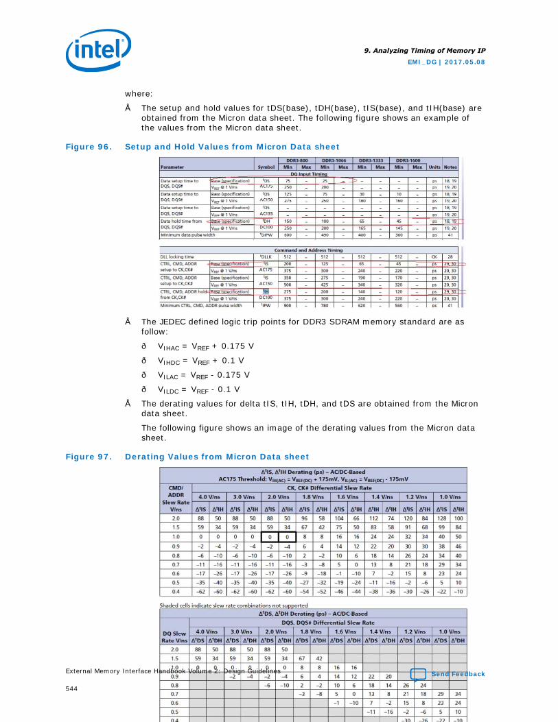
where:
• The setup and hold values for tDS(base), tDH(base), tIS(base), and tIH(base) areobtained from the Micron data sheet. The following figure shows an example ofthe values from the Micron data sheet.
Figure 96. Setup and Hold Values from Micron Data sheet
• The JEDEC defined logic trip points for DDR3 SDRAM memory standard are asfollow:
— VIHAC = VREF + 0.175 V
— VIHDC = VREF + 0.1 V
— VILAC = VREF - 0.175 V
— VILDC = VREF - 0.1 V
• The derating values for delta tIS, tIH, tDH, and tDS are obtained from the Microndata sheet.
The following figure shows an image of the derating values from the Micron datasheet.
Figure 97. Derating Values from Micron Data sheet
9. Analyzing Timing of Memory IP
EMI_DG | 2017.05.08
External Memory Interface Handbook Volume 2: Design Guidelines Send Feedback
544
Related Information
• www.micron.com
• Micron DDR3 Data Sheet
• www.jedec.org
9.13.2.3. Intersymbol Interference
ISI parameters are similarly auto-populated based on the number of ranks you selectwith Intel's PCB simulations. You can update these autopopulated typical values, ifmore accurate dedicated simulation results are available.
Intel recommends performing board-level simulations to calculate the slew rate andISI deltas that account for accurate board level effects for your board. You can useHyperLynx or similar simulators to obtain these simulation numbers. The defaultvalues have been computed using HyperLynx simulations for Intel boards with multipleDDR2 and DDR3 SDRAM slots.
The wizard writes these parameters for the slew rates and the ISI into the .sdc andthey are used during timing analysis.
9.13.2.4. Measuring Eye Reduction for Address/Command, DQ, and DQS Setupand Hold Time
This topic describes how to measure eye reduction for address/command, DQ, andDQS.
Channel signal integrity is a measure of the distortion of the eye due to intersymbolinterference or crosstalk or other effects. Typically, when going from a single-rankconfiguration to a multi-rank configuration there is an increase in the channel loss dueto reflections caused by multiple stubs. Although the Quartus Prime timing modelincludes some channel uncertainty, you must perform your own channel signalintegrity simulations and enter the additional channel uncertainty, as compared to thereference eye, into the parameter editor.
For details about measuring channel signal integrity, refer to Measuring Channel SignalIntegrity, on www.alterawiki.com.
Related Information
http://alterawiki.com/wiki/Measuring_Channel_Signal_Integrity
9.14. Early I/O Timing Estimation for Arria 10 EMIF IP
Early I/O timing analysis allows you to run I/O timing analysis without first compilingyour design. You can use early I/O timing analysis to quickly evaluate whetheradequate timing margin exists on the I/O interface between the FPGA and externalmemory device.
9. Analyzing Timing of Memory IP
EMI_DG | 2017.05.08
Send Feedback External Memory Interface Handbook Volume 2: Design Guidelines
545
Early I/O timing analysis performs the following analyses:
• Read analysis
• Write analysis
• Address and command analysis
• DQS gating analysis
• Write leveling analysis
Early I/O timing analysis takes into consideration the following factors:
• The timing parameters of the memory device
• The speed and topology of the memory interface
• The board timing and ISI characteristics
• The timing of the selected FPGA device
9.14.1. Performing Early I/O Timing Analysis for Arria 10 EMIF IP
To perform early I/O timing analysis, follow these steps:
1. Instantiate an Arria 10 EMIF IP core.
a. On the Memory Timing tab, enter accurate memory parameters.
b. On the Board Timing tab, enter accurate values for Slew Rate, IntersymbolInterference, and Board and Package Skews.
2. After generating your IP core, create a Quartus Prime project and select yourdevice from the Available devices list.
3. To launch the TimeQuest Timing Analyzer, select TimeQuest Timing Analyzerfrom the Tools menu.
4. To run early I/O timing analysis:
a. Select Run Tcl Script from the Script menu.
b. Run submodule\<variation_name>_report_io_timing.tcl.
The following figure shows an early I/O timing analysis from the TimeQuest TimingAnalyzer using a DDR3 example design.
9. Analyzing Timing of Memory IP
EMI_DG | 2017.05.08
External Memory Interface Handbook Volume 2: Design Guidelines Send Feedback
546
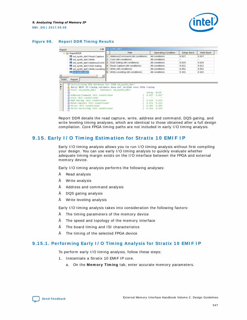
Figure 98. Report DDR Timing Results
Report DDR details the read capture, write, address and command, DQS gating, andwrite leveling timing analyses, which are identical to those obtained after a full designcompilation. Core FPGA timing paths are not included in early I/O timing analysis.
9.15. Early I/O Timing Estimation for Stratix 10 EMIF IP
Early I/O timing analysis allows you to run I/O timing analysis without first compilingyour design. You can use early I/O timing analysis to quickly evaluate whetheradequate timing margin exists on the I/O interface between the FPGA and externalmemory device.
Early I/O timing analysis performs the following analyses:
• Read analysis
• Write analysis
• Address and command analysis
• DQS gating analysis
• Write leveling analysis
Early I/O timing analysis takes into consideration the following factors:
• The timing parameters of the memory device
• The speed and topology of the memory interface
• The board timing and ISI characteristics
• The timing of the selected FPGA device
9.15.1. Performing Early I/O Timing Analysis for Stratix 10 EMIF IP
To perform early I/O timing analysis, follow these steps:
1. Instantiate a Stratix 10 EMIF IP core.
a. On the Memory Timing tab, enter accurate memory parameters.
9. Analyzing Timing of Memory IP
EMI_DG | 2017.05.08
Send Feedback External Memory Interface Handbook Volume 2: Design Guidelines
547
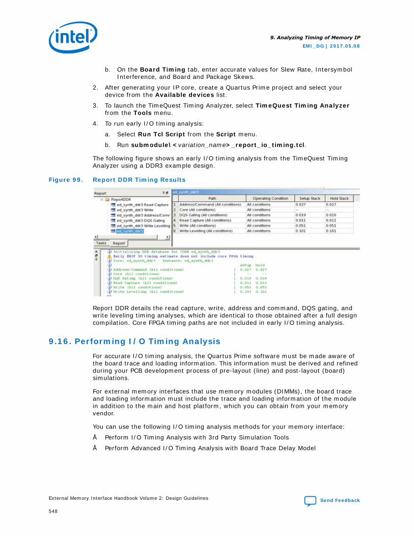
b. On the Board Timing tab, enter accurate values for Slew Rate, IntersymbolInterference, and Board and Package Skews.
2. After generating your IP core, create a Quartus Prime project and select yourdevice from the Available devices list.
3. To launch the TimeQuest Timing Analyzer, select TimeQuest Timing Analyzerfrom the Tools menu.
4. To run early I/O timing analysis:
a. Select Run Tcl Script from the Script menu.
b. Run submodule\<variation_name>_report_io_timing.tcl.
The following figure shows an early I/O timing analysis from the TimeQuest TimingAnalyzer using a DDR3 example design.
Figure 99. Report DDR Timing Results
Report DDR details the read capture, write, address and command, DQS gating, andwrite leveling timing analyses, which are identical to those obtained after a full designcompilation. Core FPGA timing paths are not included in early I/O timing analysis.
9.16. Performing I/O Timing Analysis
For accurate I/O timing analysis, the Quartus Prime software must be made aware ofthe board trace and loading information. This information must be derived and refinedduring your PCB development process of pre-layout (line) and post-layout (board)simulations.
For external memory interfaces that use memory modules (DIMMs), the board traceand loading information must include the trace and loading information of the modulein addition to the main and host platform, which you can obtain from your memoryvendor.
You can use the following I/O timing analysis methods for your memory interface:
• Perform I/O Timing Analysis with 3rd Party Simulation Tools
• Perform Advanced I/O Timing Analysis with Board Trace Delay Model
9. Analyzing Timing of Memory IP
EMI_DG | 2017.05.08
External Memory Interface Handbook Volume 2: Design Guidelines Send Feedback
548
Related Information
• Performing I/O Timing Analysis with Third-Party Simulation Tools on page 549
• Performing Advanced I/O Timing Analysis with Board Trace Delay Model on page549
9.16.1. Performing I/O Timing Analysis with Third-Party Simulation Tools
Intel recommends that you perform I/O timing analysis using the third-partysimulation tool flow because this flow involves post layout simulation that can capturemore accurate I/O timing. This method is also easier because it only requires you toenter the slew rates, board skews, and ISI values in the parameter editor.
To perform I/O timing analysis using third-party simulation tools, follow these steps:
1. Use a third-party simulation tool such as HyperLynx to simulate the full path forDQ, DQS, CK, Address, and Command signals.
2. Under the Board Settings tab of the parameter editor, enter the slowest slewrate, ISI, and board skew values.
9.16.2. Performing Advanced I/O Timing Analysis with Board Trace DelayModel
You should use this method only if you are unable to perform post-layout simulationon the memory interface signals to obtain the slew rate parameters, and/or when nosimulation tool is available.
To perform I/O timing analysis using board trace delay model, follow these steps:
1. After the instantiation is complete, analyze and synthesize your design.
2. Add pin and DQ group assignment by running the<variation_name>_p0_pin_assignments.tcl script.
Note: The naming of the pin assignment file may vary depending on theQuartus Prime software version that you are using.
3. Enter the pin location assignments.
4. Assign the virtual pins, if necessary.
5. Enter the board trace model information. To enter board trace model information,follow these steps:
a. In the Pin Planner, select the pin or group of pins for which you want to enterboard trace parameters.
b. Right-click and select Board Trace Model.
6. Compile your design. To compile the design, on the Processing menu, click StartCompilation.
7. After successfully compiling the design, perform timing analysis in the TimeQuesttiming analyzer. To perform timing analysis, follow these steps:
a. In the Quartus Prime software, on the Tools menu, click TimeQuest TimingAnalyzer.
b. On the Tasks pane, click Report DDR.
c. On the Report pane, select Advanced I/O Timing>Signal IntegrityMetrics.
9. Analyzing Timing of Memory IP
EMI_DG | 2017.05.08
Send Feedback External Memory Interface Handbook Volume 2: Design Guidelines
549
d. In the Signal Integrity Metrics window, right-click and select Regenerateto regenerate the signal integrity metrics.
e. In the Signal Integrity Metrics window, note the 10–90% rise time (or falltime if fall time is worse) at the far end for CK/CK#, address, and command,DQS/DQS#, and DQ signals.
f. In the DDR3 SDRAM controller parameter editor, in the Board Settings tab,type the values you obtained from the signal integrity metrics.
g. For the board skew parameters, set the maximum skew within DQS groups ofyour design. Set the other board parameters to 0 ns.
h. Compile your design.
9.17. Document Revision History
Date Version Changes
May 2017 2017.05.08 • Added Timing Constraint and Report Files for Stratix 10 EMIF IP, TimingAnalysis Description for Stratix 10 EMIF IP, and Early I/O TimingEstimation for Stratix 10 EMIF IP sections.
• Rebranded as Intel.
October 2016 2016.10.31 Maintenance release.
May 2016 2016.05.02 Maintenance release.
November 2015 2015.11.02 Changed instances of Quartus II to Quartus Prime.
May 2015 2015.05.04 Maintenance release.
December 2014 2014.12.15 Maintenance release.
August 2014 2014.08.15 Removed occurrences of MegaWizard Plug-In Manager.
December 2013 2013.12.16 • Removed references to ALTMEMPHY.• Removed references to HardCopy.• Removed references to Stratix II devices.• Removed references to Cyclone III and Cyclone IV devices.• Added information for Arria 10 support.
November 2012 6.0 Changed chapter number from 10 to 11.
June 2012 5.0 Added Feedback icon.
November 2011 4.0 • Added Arria V and Cyclone V information.• Added Performing I/O Timing Analysis section.• Added Measuring Eye Reduction for Address/Command, DQ, and DQS
Setup and Hold Time section.
June 2011 3.0 Updated for 11.0 release.
December 2010 2.1 Added Arria II GZ and Stratix V, updated board skews table.
July 2010 2.0 Added information about UniPHY-based IP and controllers.
January 2010 1.2 Corrected typos.
December 2009 1.1 Added Timing Deration section.
November 2009 1.0 Initial release.
9. Analyzing Timing of Memory IP
EMI_DG | 2017.05.08
External Memory Interface Handbook Volume 2: Design Guidelines Send Feedback
550
10. Debugging Memory IPThe following topics describe the tools and processes for debugging external memoryinterfaces.
The discussion focuses on issues pertaining to the Intel DDR, DDR2, DDR3, DDR4,LPDDR2, LPDDR3, QDRII, QDRII+, QDRII+ Xtreme, QDR-IV, RLDRAM II, and RLDRAM3 IP.
In general, memory debugging issues can be categorized as follows:
• Resource and planning issues
• Interface configuration issues
• Functional issues
• Timing issues
Some issues may not be directly related to interface operation; problems can alsooccur at the Quartus Prime Fitter stage, or in timing analysis.
10.1. Resource and Planning Issues
Typically, single stand-alone interfaces should not present Quartus Prime Fitter ortiming problems.
You may find that fitter, timing, and hardware operation can sometimes become achallenge, as multiple interfaces are combined into a single project, or as the deviceutilization increases. In such cases, interface configuration is not the issue; rather, theplacement and total device resource requirements can create problems.
Resource Issue Evaluation
External memory interfaces typically require the following resource types, which youmust consider when trying to place logic manually. You might also use additionalconstraints to force the placement or location of external memory interface IP:
• Dedicated IOE DQS group resources and pins
• Dedicated DLL resources
• Specific PLL resources
• Specific global, regional, and dual-regional clock net resources
10.1.1. Dedicated IOE DQS Group Resources and Pins
Fitter issues can occur with even a single interface, if you do not size the interface tofit within the specified constraints and requirements. A typical requirement includescontaining assignments for the interface within a single bank or possibly side of thechosen device.
EMI_DG | 2017.05.08
Send Feedback
Intel Corporation. All rights reserved. Intel, the Intel logo, Altera, Arria, Cyclone, Enpirion, MAX, Nios, Quartusand Stratix words and logos are trademarks of Intel Corporation or its subsidiaries in the U.S. and/or othercountries. Intel warrants performance of its FPGA and semiconductor products to current specifications inaccordance with Intel's standard warranty, but reserves the right to make changes to any products and servicesat any time without notice. Intel assumes no responsibility or liability arising out of the application or use of anyinformation, product, or service described herein except as expressly agreed to in writing by Intel. Intelcustomers are advised to obtain the latest version of device specifications before relying on any publishedinformation and before placing orders for products or services.*Other names and brands may be claimed as the property of others.
ISO9001:2015Registered
Such a constraint requires that the chosen device meets the following conditions:
• Sufficient DQS groups and sizes to support the required number of common I/O(CIO) or separate I/O (SIO) data groups.
• Sufficient remaining pins to support the required number of address, command,and control pins.
Failure to evaluate these fundamental requirements can result in suboptimal interfacedesign, if the chosen device cannot be modified. The resulting wraparound interfacesor suboptimal pseudo read and write data groups artificially limit the maximumoperating frequency.
Multiple blocks of IP further complicate the issue, if other IP has either no specifiedlocation constraints or incompatible location constraints.
The Quartus Prime fitter may first place other components in a location required byyour memory IP, then error at a later stage because of an I/O assignment conflictbetween the unconstrained IP and the constrained memory IP.
Your design may require that one instance of IP is placed anywhere on one side of thedevice, and that another instance of IP is placed at a specific location on the sameside.
While the two individual instances may compile in isolation, and the physical numberof pins may appear sufficient for both instances, issues can occur if the instancewithout placement constraints is placed before the instance with placementconstraints.
In such circumstances, Intel recommends manually placing each individual pin, or atleast try using more granular placement constraints.
For more information about the pin number and DQS group capabilities of your chosendevice, refer to device data sheets or the Quartus Prime Pin Planner.
10.1.2. Dedicated DLL Resources
Intel devices typically use DLLs to enhance data capture at the FPGA. While multipleexternal memory interfaces can usually share DLL resources, fitter issues can occurwhen there is insufficient planning before HDL coding.
If DLL sharing is required, Intel gives the following recommendations for each instanceof the IP that shares the DLL resources:
• Must have compatible DLL requirements—same frequency and mode.
• Exports its autogenerated DLL instance out of its own dedicated PHY hierarchy andinto the top-level design file. This procedure allows easy comparison of thegenerated DLL’s mode, and allows you to explicitly show the required DLL sharingbetween two IP blocks in the HDL
Note: The Quartus Prime fitter does not dynamically merge DLL instances.
10. Debugging Memory IP
EMI_DG | 2017.05.08
External Memory Interface Handbook Volume 2: Design Guidelines Send Feedback
552
10.1.3. Specific PLL Resources
When only a single interface resides on one side or one quadrant of a device, PLLresources are typically not an issue. However if multiple interfaces or IP are requiredon a single side or quadrant, consider the specific PLL used by each IP, and thesharing of any PLL resources.
The Quartus Prime software automerges PLL resources, but not for any dynamicallycontrolled PLL components. Use the following PLL resource rules:
• Ensure that the PLL located in the same bank or side of the device is available foryour memory controller.
• If multiple PLLs are required for multiple controllers that cannot be shared, ensurethat enough PLL resources are available within each quadrant to support yourinterface number requirements.
• Try to limit multiple interfaces to a single quadrant. For example, if two completesame size interfaces can fit on a single side of the device, constrain one interfaceentirely in one bank of that side, and the other controller in the other bank.
For more information about using multiple PHYs or controllers, refer to the designtutorials on the List of designs using Intel External Memory IP page ofwww.alterawiki.com.
Related Information
List of designs using Intel FPGA External Memory IP
10.1.4. Specific Global, Regional and Dual-Regional Clock Net Resources
Memory PHYs typically have specific clock resource requirements for each PLL clockoutput.
For example because of characterization data, the PHY may require that the phy_clkis routed on a global clock net. The remaining clocks may all be routed on a global ora regional clock net. However, they must all be routed on the same type. Otherwise,the operating frequency of the interface is lowered, because of the increaseduncertainty between two different types of clock nets. The design may still fit, but notmeet timing.
10.1.5. Planning Your Design
It is important to understand your design and to plan its resource usage and layout.Include the following steps in your design planning:
10. Debugging Memory IP
EMI_DG | 2017.05.08
Send Feedback External Memory Interface Handbook Volume 2: Design Guidelines
553
1. Plan the total number of DQS groups and total number of other pins required inyour shared area. Use the Pin Planner to assist with this activity.
2. Decide which PLLs or clock networks can be shared between IP blocks, thenensure that sufficient resources are available. For example, if an IP core requires aregional clock network, a PLL located on the opposite side of the device cannot beused.
3. Calculate the number of total clock networks and types required when trying tocombine multiple instances of IP.
4. You must understand the number of quadrants that the IP uses and if this numbercan be reduced. For example, an interface may be autoplaced across an entireside of the device, but may actually be constrained to fit in a single bank.
By optimizing physical placement, you ensure that the system uses regional clocknetworks whereever possible. The use of regional clock networks instead of dual-regional clock networks can help maintain clock net resources and simplify routing.
10.1.6. Optimizing Design Utilization
As device utilization increases, the Quartus Prime software may have difficulty placingthe core. To optimize design utilization, follow these steps:
1. Review any fitter warning messages in multiple IP designs to ensure that clocknetworks or PLL modes are not modified to achieve the desired fit.
2. Use the Quartus Prime Fitter resource section to compare the types of resourcesused in a successful standalone IP implementation to those used in an unreliablemultiple IP implementation.
3. Use this information to better constrain the project to achieve the same results asthe standalone project.
4. Use the Chip Planner (Floorplan and Chip Editor) to compare the placement of theworking stand-alone design to the multiple IP project. Then use LogicLock™ orDesign Partitions to better guide the Quartus Prime software to the requiredresults.
5. When creating LogicLock regions, ensure that they encompass all requiredresources. For example, if constraining the read and write datapath hierarchy,ensure that your LogicLock region includes the IOE blocks used for your datapathpin out.
10.2. Interface Configuration Performance Issues
There are a large number of interface combinations and configurations possible in anIntel design, therefore it is impractical for Intel to explicitly state the achievable fMAXfor every combination.
Intel seeks to provide guidance on typical performance, but this data is subject tomemory component timing characteristics, interface widths, depths directly affectingtiming deration requirements, and the achieved skew and timing numbers for aspecific PCB.
FPGA timing issues should generally not be affected by interface loading or layoutcharacteristics. In general, the Intel performance figures for any given device familyand speed-grade combination should usually be achievable.
10. Debugging Memory IP
EMI_DG | 2017.05.08
External Memory Interface Handbook Volume 2: Design Guidelines Send Feedback
554
To resolve FPGA (PHY and PHY reset) timing issues, refer to the Analyzing Timing ofMemory IP chapter.
Achievable interface timing (address and command, half-rate address and command,read and write capture) is directly affected by any layout issues (skew), loading issues(deration), signal integrity issues (crosstalk timing deration), and component speedgrades (memory timing size and tolerance). Intel performance figures are typicallystated for the default (single rank, unbuffered DIMM) case. Intel provides additionalexpected performance data where possible, but the fMAX is not achievable in allconfigurations. Intel recommends that you optimize the following items wheneverinterface timing issues occur:
• Improve PCB layout tolerances
• Use a faster speed grade of memory component
• Ensure that the interface is fully and correctly terminated
• Reduce the loading (reduce the deration factor)
Related Information
Analyzing Timing of Memory IP on page 494
10.2.1. Interface Configuration Bottleneck and Efficiency Issues
Depending on the transaction types, efficiency issues can exist where the achieveddata rate is lower than expected. Ideally, these issues should be assessed andresolved during the simulation stage because they are sometimes impossible to solvelater without rearchitecting the product.
Any interface has a maximum theoretical data rate derived from the clock frequency,however, in practise this theoretical data rate can never be achieved continuously dueto protocol overhead and bus turnaround times.
Simulate your desired configuration to ensure that you have specified a suitableexternal memory family and that your chosen controller configuration can achieveyour required bandwidth.
Efficiency can be assessed in several different ways, and the primary requirement isan achievable continuous data rate. The local interface signals combined with thememory interface signals and a command decode trace should provide adequatevisibility of the operation of the IP to understand whether your required data rate issufficient and the cause of the efficiency issue.
To show if under ideal conditions the required data rate is possible in the chosentechnology, follow these steps:
1. Use the memory vendors own testbench and your own transaction engine.
2. Use either your own driver, or modify the provided example driver, to replicate thetransaction types typical of your system.
3. Simulate this performance using your chosen memory controller and decide if theachieved performance is still acceptable.
10. Debugging Memory IP
EMI_DG | 2017.05.08
Send Feedback External Memory Interface Handbook Volume 2: Design Guidelines
555
Observe the following points that may cause efficiency or bottleneck issues at thisstage:
• Identify the memory controller rate (full, half, or quarter) and commands, whichmay take two or four times longer than necessary
• Determine whether the memory controller is starved for data by observing theappropriate request signals.
• Determine whether the memory controller processor transactions at a ratesufficient to meet throughput requirements by observing appropriate signals,including the local ready signal.
Intel has several versions and types of memory controller, and where possible you canevaluate different configurations based on the results of the first tests.
Consider using either a faster interface, or a different memory type to better alignyour data rate requirements to the IP available directly from Intel.
Intel also provides stand-alone PHY configurations so that you may develop customcontrollers or use third-party controllers designed specifically for your requirements.
10.3. Functional Issue Evaluation
Functional issues occur at all frequencies (using the same conditions) and are notaltered by speed grade, temperature, or PCB changes. You should use functionalsimulation to evaluate functional issues.
The Intel FPGA IP includes the option to autogenerate a testbench specific to your IPconfiguration, which provides an easy route to functional verification.
The following issues should be considered when trying to debug functional issues in asimulation environment.
10.3.1. Correct Combination of the Quartus Prime Software and ModelSim- Intel FPGA Edition Device Models
When running any simulations, ensure that you are using the correct combination ofthe Quartus Prime software and device models.
Intel only tests each release of software and IP with the aligned release of devicemodels. Failure to use the correct RTL and model combination may result in unstablesimulation environments.
The ModelSim - Intel FPGA Edition comes precompiled with the Intel device familylibraries included. You must always install the correct release of ModelSim - Intel FPGAEdition to align with your Quartus Prime software and IP release.
If you are using a full version of ModelSim, or any other supported simulationenvironment, ensure that you are compiling the current Quartus Prime suppliedlibraries. These libraries are located in the <Quartus Prime install path>/quartus/eda/sim_lib/ directory.
10. Debugging Memory IP
EMI_DG | 2017.05.08
External Memory Interface Handbook Volume 2: Design Guidelines Send Feedback
556
10.3.2. Intel IP Memory Model
Intel memory IP autogenerates a generic simplified memory model that works in allcases. This simple read and write model is not designed or intended to verify allentered IP parameters or transaction requirements.
The Intel-generated memory model may be suitable to evaluate some limitedfunctional issues, but it does not provide comprehensive functional simulation.
10.3.3. Vendor Memory Model
Contact the memory vendor directly, because many additional models are availablefrom the vendor's support system.
When using memory vendor models, ensure that the model is correctly defined for thefollowing characteristics:
• Speed grade
• Organization
• Memory allocation
• Maximum memory usage
• Number of ranks on a DIMM
• Buffering on the DIMM
• ECC
Note: Refer to the readme.txt file supplied with the memory vendor model, for moreinformation about how to define this information for your configuration. Also refer toTranscript Window Messages, for more information.
Note: Intel does not provide support for vendor-specific memory models.
During simulation vendor models output a wealth of information regarding any deviceviolations that may occur because of incorrectly parameterized IP.
10.3.4. Insufficient Memory in Your PC
If you are running the ModelSim - Intel FPGA Edition simulator, the limitation onmemory size may mean that you have insufficient memory to run your simulation. Or,if you are using a 32-bit operating system, your PC may have insufficient memory.
Typical simulation tool errors include: "Iteration limit reached" or "Error out ofmemory".
When using either the Intel generic memory model, or a vendor specific model quitelarge memory depths can be required if you do not specify your simulation carefully.
For example, if you simulate an entire 4-GB DIMM interface, the hardware platformthat performs that simulation requires at least this amount of memory just for thesimulation contents storage.
Note: Refer to Memory Allocation and Max Memory Usage in the vendor's readme.txt filesfor more information.
10. Debugging Memory IP
EMI_DG | 2017.05.08
Send Feedback External Memory Interface Handbook Volume 2: Design Guidelines
557

10.3.5. Transcript Window Messages
When you are debugging a functional issue in simulation, vendor models typicallyprovide much more detailed checks and feedback regarding the interface and theiroperational requirements than the Intel generic model.
In general, you should use a vendor-supplied model whenever one is available.Consider using second-source vendor models in preference to the Intel generic model.
Many issues can be traced to incorrectly configured IP for the specified memorycomponents. Component data sheets usually contain settings information for severaldifferent speed grades of memory. Be aware data sheet specify parameters in fixedunits of time, frequencies, or clock cycles.
The Intel generic memory model always matches the parameters specified in the IP,as it is generated using the same engine. Because vendor models are independent ofthe IP generation process, they offer a more robust IP parameterization check.
During simulation, review the transcript window messages and do not rely on theSimulation Passed message at the end of simulation. This message only indicates thatthe example driver successfully wrote and then read the correct data for a single testcycle.
Even if the interface functionally passes in simulation, the vendor model may reportoperational violations in the transcript window. These reported violations oftenspecifically explain why an interface appears to pass in simulation, but fails inhardware.
Vendor models typically perform checks to ensure that the following types ofparameters are correct:
• Burst length
• Burst order
• tMRD
• tMOD
• tRFC
• tREFPDEN
• tRP
• tRAS
• tRC
• tACTPDEN
• tWR
• tWRPDEN
• tRTP
• tRDPDEN
• tINIT
• tXPDLL
• tCKE
• tRRD
10. Debugging Memory IP
EMI_DG | 2017.05.08
External Memory Interface Handbook Volume 2: Design Guidelines Send Feedback
558
• tCCD
• tWTR
• tXPR
• PRECHARGE
• CAS length
• Drive strength
• AL
• tDQS
• CAS_WL
• Refresh
• Initialization
• tIH
• tIS
• tDH
• tDS
If a vendor model can verify all these parameters are compatible with your chosencomponent values and transactions, it provides a specific insight into hardwareinterface failures.
10.3.6. Passing Simulation
Passing simulation means that the interface calibrates and successfully completes asingle test complete cycle without asserting pass not fail (pnf).
It does not take into account any warning messages that you may receive duringsimulation. If you are debugging an interface issue, review and, if necessary, correctany warning messages from the transcript window before continuing.
10.3.7. Modifying the Example Driver to Replicate the Failure
Often during debugging, you may discover that the example driver design workssuccessfully, but that your custom logic encounters data errors.
When the example design works but your custom design doesn't, the underlyingproblem may be either of the following:
• Related to the way that the local interface transactions are occurring. You shouldprobe and compare using the Signal Tap II analyzer.
• Related to the types or format of transactions on the external memory interface.You should try modifying the example design to replicate the problem.
10. Debugging Memory IP
EMI_DG | 2017.05.08
Send Feedback External Memory Interface Handbook Volume 2: Design Guidelines
559
Typical issues on the local interface side include:
• Incorrect local-address-to-memory-address translation causing the word order tobe different than expected. Refer to Burst Definition in your memory vendor datasheet.
• Incorrect timing on the local interface. When your design requests a transaction,the local side must be ready to service that transaction as soon as it is acceptedwithout any pause.
• For more information, refer to the Avalon® Interface Specification .
The default example driver performs only a limited set of transaction types,consequently potential bus contention or preamble and postamble issues can often bemasked in its default operation. For successful debugging, isolate the custom logictransaction types that are causing the read and write failures and modify the exampledriver to demonstrate the same issue. Then, you can try to replicate the failure in RTLsimulation with the modified driver.
For Arria 10 and Stratix 10 interfaces, you can enable the Traffic Generator 2.0 in theexample design, allowing you to use the EMIF Debug Toolkit to configure differenttraffic pattern for debug purposes.
A problem that you can replicate in RTL simulation indicates a potential bug in the IP.You should recheck the IP parameters. A problem that you can not replicate in RTLsimulation indicates a timing issue on the PCB. You can try to replicate the issue on anIntel development platform to rule out a board issue.
Note: Ensure that all PCB timing, loading, skew, and deration information is correctly definedin the Quartus Prime software. The timing report is inaccurate if this initial data is notcorrect.
Functional simulation allows you to identify any issues with the configuration of eitherthe memory controller or the PHY. You can then check the operation against both thememory vendor data sheet and the respective JEDEC specification. After you resolvefunctional issues, you can start testing hardware.
For more information about simulation, refer to the Simulating Memory IP chapter.
Related Information
• Avalon Interface Specification
• Simulating Memory IP on page 468
10.4. Timing Issue Characteristics
The Altera PHY and controller combinations autogenerate timing constraint files toensure that the PHY and external interface are fully constrained and that timing isanalyzed during compilation. However, timing issues can still occur. This topicdiscusses how to identify and resolve any timing issues that you may encounter.
Timing issues typically fall into two distinct categories:
• FPGA core timing reported issues
• External memory interface timing issues in a specific mode of operation or on aspecific PCB
10. Debugging Memory IP
EMI_DG | 2017.05.08
External Memory Interface Handbook Volume 2: Design Guidelines Send Feedback
560
TimeQuest reports timing issues in two categories: core to core and core to IOEtransfers. These timing issues include the PHY and PHY reset sections in theTimeQuest Report DDR subsection of timing analysis. External memory interfacetiming issues are specifically reported in the TimeQuest Report DDR subsection,excluding the PHY and PHY reset. The Report DDR PHY and PHY reset sections onlyinclude the PHY, and specifically exclude the controller, core, PHY-to-controller andlocal interface. Quartus Prime timing issues should always be evaluated and correctedbefore proceeding to any hardware testing.
PCB timing issues are usually Quartus Prime timing issues, which are not reported inthe Quartus Prime software, if incorrect or insufficient PCB topology and layoutinformation is not supplied. PCB timing issues are typically characterized by calibrationfailure, or failures during user mode when the hardware is heated or cooled. FurtherPCB timing issues are typically hidden if the interface frequency is lowered.
10.4.1. Evaluating FPGA Timing Issues
Usually, you should not encounter timing issues with Intel-provided IP unless yourdesign exceeds Intel's published performance range or you are using a device forwhich the Quartus Prime software offers only preliminary timing model support.Nevertheless, timing issues can occur in the following circumstances:
• The .sdc files are incorrectly added to the Quartus Prime project
• Quartus Prime analysis and synthesis settings are not correct
• Quartus Prime Fitter settings are not correct
For all of these issues, refer to the correct user guide for more information aboutrecommended settings and follow these steps:
1. Ensure that the IP generated .sdc files are listed in the Quartus Prime TimeQuestTiming Analyzer files to include in the project window.
2. Ensure that Analysis and Synthesis Settings are set to OptimizationTechnique Speed .
3. Ensure that Fitter Settings are set to Fitter Effort Standard Fit .
4. Use TimeQuest Report Ignored Constraints, to ensure that .sdc files aresuccessfully applied.
5. Use TimeQuest Report Unconstrained Paths, to ensure that all critical pathsare correctly constrained.
More complex timing problems can occur if any of the following conditions are true:
• The design includes multiple PHY or core projects
• Devices where the resources are heavily used
• The design includes wide, distributed, maximum performance interfaces in largedie sizes
Any of the above conditions can lead to suboptimal placement results when the PHY orcontroller are distributed around the FPGA. To evaluate such issues, simplify thedesign to just the autogenerated example top-level file and determine if the coremeets timing and you see a working interface. Failure implies that a morefundamental timing issue exists. If the standalone design passes core timing, evaluatehow this placement and fit is different than your complete design.
10. Debugging Memory IP
EMI_DG | 2017.05.08
Send Feedback External Memory Interface Handbook Volume 2: Design Guidelines
561
Use LogicLock regions, or design partitions to better define the placement of yourmemory controllers. When you have your interface standalone placement, repeat foradditional interfaces, combine, and finally add the rest of your design.
Additionally, use fitter seeds and increase the placement and router effort multiplier.
10.4.2. Evaluating External Memory Interface Timing Issues
External memory interface timing issues usually relate to the FPGA input and outputcharacteristics, PCB timing, and the memory component characteristics.
The FPGA input and output characteristics are usually fixed values, because the IOEstructure of the devices is fixed. Optimal PLL characteristics and clock routingcharacteristics do have an effect. Assuming the IP is correctly constrained withautogenerated assignments, and you follow implementation rules, the design shouldreach the stated performance figures.
Memory component characteristics are fixed for any given component or DIMM.Consider using faster components or DIMMs in marginal cases when PCB skew may besuboptimal, or your design includes multiple ranks when deration may cause readcapture or write timing challenges. Using faster memory components often reducesthe memory data output skew and uncertainty easing read capture, and lowering thememory’s input setup and hold requirement, which eases write timing.
Increased PCB skew reduces margins on address, command, read capture and writetiming. If you are narrowly failing timing on these paths, consider reducing the boardskew (if possible), or using faster memory. Address and command timing typicallyrequires you to manually balance the reported setup and hold values with thededicated address and command phase in the IP.
Refer to the respective IP user guide for more information.
Multiple-slot multiple-rank UDIMM interfaces can place considerable loading on theFPGA driver. Typically a quad rank interface can have thirty-six loads. In multiple-rankconfigurations, Intel's stated maximum data rates are not likely to be achievablebecause of loading deration. Consider using different topologies, for exampleregistered DIMMs, so that the loading is reduced.
Deration because of increased loading, or suboptimal layout may result in a lower thandesired operating frequency meeting timing. You should close timing in the QuartusPrime software using your expected loading and layout rules before committing to PCBfabrication.
Ensure that any design with an Altera PHY is correctly constrained and meets timing inthe Quartus Prime software. You must address any constraint or timing failures beforetesting hardware.
For more information about timing constraints, refer to the Analyzing Timing ofMemory IP chapter.
Related Information
Analyzing Timing of Memory IP on page 494
10.5. Verifying Memory IP Using the Signal Tap II Logic Analyzer
The Signal Tap II logic analyzer shows read and write activity in the system.
10. Debugging Memory IP
EMI_DG | 2017.05.08
External Memory Interface Handbook Volume 2: Design Guidelines Send Feedback
562
For more information about using the Signal Tap II logic analyzer, refer to the DesignDebugging Using the Signal Tap II Embedded Logic Analyzer chapter in volume 3 ofthe Quartus Prime Handbook
To add the Signal Tap II logic analyzer, follow these steps:
1. On the Tools menu click Signal Tap II Logic Analyzer .
2. In the Signal Configuration window next to the Clock box, click … (BrowseNode Finder).
3. Type the memory interface system clock (typically * phy_clk) in the Named box,for Filter select Signal Tap II: presynthesis and click List.
4. Select the memory interface clock that is exposed to the user logic.
5. Click OK.
6. Under Signal Configuration, specify the following settings:
• For Sample depth, select 512
• For RAM type, select Auto
• For Trigger flow control, select Sequential
• For Trigger position, select Center trigger position
• ForTrigger conditions , select 1
7. On the Edit menu, click Add Nodes.
8. Search for specific nodes that you want to monitor, and click Add.
Note: Signal Tap can probe only nodes that are exposed to FPGA core logic. Referto pin descriptions in the in the External Memory Interface Handbook forhelp in deciding which signals to monitor.
9. Decide which signal and event you want to trigger on, and set the correspondingtrigger condition.
10. On the File menu, click Save, to save the Signal Tap II . stp file to your project.
Note: If you see the message Do you want to enable Signal Tap II file“stp1.stp” for the current project, click Yes.
11. After you add signals to the Signal Tap II logic analyzer, recompile your design byclicking Start Compilation on the Processing menu.
12. Following compilation, verify that TimeQuest timing analysis passes successfully.
13. Connect the development board to your computer.
14. On the Tools menu, click Signal Tap II Logic Analyzer.
15. Add the correct <project_name>.sof file to the SOF Manager:
a. Click ... to open the Select Program Files dialog box.
b. Select <your_project_name>.sof.
c. Click Open.
d. To download the file, click the Program Device button.
16. When the example design including Signal Tap II successfully downloads to yourdevelopment board, click Run Analysis to run once, or click Autorun Analysis torun continuously.
10. Debugging Memory IP
EMI_DG | 2017.05.08
Send Feedback External Memory Interface Handbook Volume 2: Design Guidelines
563
Related Information
Design Debugging Using the Signal Tap Logic Analyzer
10.5.1. Signals to Monitor with the Signal Tap II Logic Analyzer
This topic lists the memory controller signals you should consider analyzing fordifferent memory interfaces. This list is not exhaustive, but is a starting point.
For a description of each signal, refer to Volume 3: Reference Material of the ExternalMemory Interface Handbook.
Monitor the following signals for UniPHY designs:
• avl_addr
• avl_rdata
• avl_rdata_valid
• avl_read_req
• avl_ready
• avl_wdata
• avl_write_req
• fail
• pass
• afi_cal_fail
• afi_cal_success
• test_complete
• be_reg (QDRII only)
• pnf_per_bit
• rdata_reg
• rdata_valid_reg
• data_out
• data_in
• written_data_fifo|data_out
• usequencer|state *
• usequencer|phy_seq_rdata_valid
• usequencer|phy_seq_read_fifo_q
• usequencer|phy_read_increment_vfifo *
• usequencer|phy_read_latency_counter
• uread_datapath|afi_rdata_en
• uread_datapath|afi_rdata_valid
10. Debugging Memory IP
EMI_DG | 2017.05.08
External Memory Interface Handbook Volume 2: Design Guidelines Send Feedback
564
• uread_datapath|ddio_phy_dq
• qvld_wr_address *
• qvld_rd_address *
Related Information
Volume 3: Reference Material
10.6. Hardware Debugging Guidelines
Before debugging your design, confirm that it follows the recommended design flow.Refer to the Design Flow chapter in volume 1 of the External Memory InterfaceHandbook.
Always keep a record of tests, to avoid repeating the same tests later. To startdebugging the design, perform the following initial steps.
Related Information
Recommended Design Flow
10.6.1. Create a Simplified Design that Demonstrates the Same Issue
To help debugging, create a simple design that replicates the problem.
A simple design should compile quickly and be easy to understand. The EMIF IPgenerates an example top-level file that is ideal for debugging. The example top-levelfile uses all the same parameters, pin-outs, and so on.
If you are using the Arria 10 or Stratix 10 example design and the Traffic Generator2.0, you can configure the traffic pattern using the EMIF Debug Toolkit.
10.6.2. Measure Power Distribution Network
Measure voltages of the various power supplies on their hardware developmentplatform over a suitable time base and with a suitable trigger.
Ensure that you use an appropriate probe and grounding scheme. In addition, take themeasurements directly on the pins or vias of the devices in question, and with thehardware operational.
10.6.3. Measure Signal Integrity and Setup and Hold Margin
Measure the signals on the PCB. When measuring any signal, consider the edge rate ofthe signal, not just its frequency. Modern FPGA devices have very fast edge rates,therefore you must use a suitable oscilloscope, probe, and grounding scheme whenyou measure the signals.
You can take measurements to capture the setup and hold time of key signal classeswith respect to their clock or strobe. Ensure that the measured setup and hold marginis at least better than that reported in the Quartus Prime software. A worse marginindicates a timing discrepancy somewhere in the project; however, this issue may notbe the cause of your problem.
10. Debugging Memory IP
EMI_DG | 2017.05.08
Send Feedback External Memory Interface Handbook Volume 2: Design Guidelines
565
10.6.4. Vary Voltage
Vary the voltage of your system, if you suspect a marginality issue.
Increasing the voltage usually causes devices to operate faster and also usuallyprovides increased noise margin.
10.6.5. Use Freezer Spray and Heat Gun
If you have an intermittent marginal issue, apply cold or heat to the interface to stressthe components.
Cooling ICs causes them to run faster, which makes timing easier. Conversely, heatingICs causes them to run slower, which makes timing more difficult.
If cooling or heating corrects the problem, it is probably a timing issue.
10.6.6. Operate at a Lower Speed
Test the interface at a lower speed. If the interface works at a lower speed, theinterface is correctly pinned out and functional.
If the interface fails at a lower speed, determine if the test is valid. Many high-speedmemory components have a minimal operating frequency, or require subtly differentconfigurations when operating at a lower speeds.
For example, DDR, DDR2, or DDR3 SDRAM typically requires modification to thefollowing parameters if you want to operate the interface at lower speeds:
• tMRD
• tWTR
• CAS latency and CAS write latency
10.6.7. Determine Whether the Issue Exists in Previous Versions ofSoftware
Hardware that works before an update to either the Quartus Prime software or thememory IP indicates that the development platform is not the issue.
However, the previous generation IP may be less susceptible to a PCB issue, maskingthe issue.
10.6.8. Determine Whether the Issue Exists in the Current Version ofSoftware
Designs are often tested using previous generations of Intel software or IP.
10. Debugging Memory IP
EMI_DG | 2017.05.08
External Memory Interface Handbook Volume 2: Design Guidelines Send Feedback
566
Projects may not be upgraded for various reasons:
• Multiple engineers are on the same project. To ensure compatibility, a commonrelease of Intel software is used by all engineers for the duration of the productdevelopment. The design may be several releases behind the current QuartusPrime software version.
• Many companies delay before adopting a new release of software so that they canfirst monitor Internet forums to get a feel for how successful other users say thesoftware is.
• Many companies never use the latest version of any software, preferring to waituntil the first service pack is released that fixes the primary issues.
• Some users may only have a license for the older version of the software and canonly use that version until their company makes the financial decision to upgrade.
• The local interface specification from Intel FPGA IP to the customer's logicsometimes changes from software release to software release. If you have alreadyspent resources designing interface logic, you may be reluctant to repeat thisexercise. If a block of code is already signed off, you may be reluctant to modify itto upgrade to newer IP from Intel.
In all of the above scenarios, you must determine if the issue still exists in the latestversion of the Intel software. Bug fixes and enhancements are added to the Intel FPGAIP every release. Depending on the nature of the bug or enhancement, it may notalways be clearly documented in the release notes.
Finally, if the latest version of the software resolves the issue, it may be easier todebug the version of software that you are using.
10.6.9. Try A Different PCB
If you are using the same Intel FPGA IP on several different hardware platforms,determine whether the problem occurs on all platforms or just on one.
Multiple instances of the same PCB, or multiple instances of the same interface, onphysically different hardware platforms may exhibit different behavior. You candetermine if the configuration is fundamentally not working, or if some form ofmarginality is involved in the issue.
Issues are often reported on the alpha build of a development platform. These areproduced in very limited numbers and often have received limited bare-board testing,or functional testing. These early boards are often more unreliable than productionquality PCBs.
Additionally, if the IP is from a previous project to help save development resources,determine whether the specific IP configuration works on a previous platform.
10.6.10. Try Other Configurations
Designs are often quite large, using multiple blocks of IP in many differentcombinations. Determine whether any other configurations work correctly on thedevelopment platform.
The full project may have multiple external memory controllers in the same device, ormay have configurations where only half the memory width or frequency is required.Find out what does and does not work to help the debugging of the issue.
10. Debugging Memory IP
EMI_DG | 2017.05.08
Send Feedback External Memory Interface Handbook Volume 2: Design Guidelines
567

10.6.11. Debugging Checklist
The following checklist is a good starting point when debugging an external memoryinterface.
Table 501. Checklist
Check Item
Try a different fit.
Check IP parameters at the operating frequency (tMRD, tWTR for example).
Ensure you have constrained your design with proper timing deration and have closed timing.
Simulate the design. If it fails in simulation, it will fail in hardware.
Analyze timing.
Place and assign RUP and RDN (OCT).
Measure the power distribution network (PDN).
Measure signal integrity.
Measure setup and hold timing.
Measure FPGA voltages.
Vary voltages.
Heat and cool the PCB.
Operate at a lower or higher frequency.
Check board timing and trace Information.
Check LVDS and clock sources, I/O voltages and termination.
Check PLL clock source, specification, and jitter.
Ensure the correct number of PLL phase steps take place during calibration. If the number stated inthe IP does not match the number, you may have manually altered the PLL.
Retarget to a smaller interface width or a single bank.
10.7. Catagorizing Hardware Issues
The following topics divide issues into categories. By determining which category (orcategories) an issue belongs in, you may be able to better focus on the cause of theissue.
Hardware issues fall into three categories:
• Signal integrity issues
• Hardware and calibration issues
• Intermittent issues
10. Debugging Memory IP
EMI_DG | 2017.05.08
External Memory Interface Handbook Volume 2: Design Guidelines Send Feedback
568
10.7.1. Signal Integrity Issues
Many design issues, including some at the protocol layer, can be traced back to signalintegrity problems. You should check circuit board construction, power systems,command, and data signaling to determine if they meet specifications.
If infrequent, random errors exist in the memory subsystem, product reliabilitysuffers. Check the bare circuit board or PCB design file. Circuit board errors can causepoor signal integrity, signal loss, signal timing skew, and trace impedance mismatches.Differential traces with unbalanced lengths or signals that are routed too closelytogether can cause crosstalk.
10.7.1.1. Characteristics of Signal Integrity Issues
Signal integrity problems often appear when the performance of the hardware designis marginal.
The design may not always initialize and calibrate correctly, or may exhibit occasionalbit errors in user mode. Severe signal integrity issues can result in total failure of aninterface at certain data rates, and sporadic component failure because of electricalstress. PCB component variance and signal integrity issues often show up as failureson one PCB, but not on another identical board. Timing issues can have a similarcharacteristic. Multiple calibration windows or significant differences in the calibrationresults from one calibration to another can also indicate signal integrity issues.
10.7.1.2. Evaluating SignaI Integrity Issues
Signal integrity problems can only really be evaluated in two ways:
• direct measurement using suitable test equipment like an oscilloscope and probe
• simulation using a tool like HyperLynx or Allegro PCB SI
Compare signals to the respective electrical specification. You should look forovershoot and undershoot, non-monotonicity, eye height and width, and crosstalk.
10.7.1.2.1. Skew
Ensure that all clocked signals, commands, addresses, and control signals arrive at thememory inputs at the same time.
Trace length variations cause data valid window variations between the signals,reducing margin. For example, DDR2-800 at 400 MHz has a data valid window that issmaller than 1,250 ps. Trace length skew or crosstalk can reduce this data validwindow further, making it difficult to design a reliably operating memory interface.Ensure that the skew figure previously entered into the Intel FPGA IP matches thatactually achieved on the PCB, otherwise Quartus Prime timing analysis of the interfaceis accurate.
10.7.1.2.2. Crosstalk
Crosstalk is best evaluated early in the memory design phase.
Check the clock-to-data strobes, because they are bidirectional. Measure the crosstalkat both ends of the line. Check the data strobes to clock, because the clocks areunidirectional, these only need checking at the memory end of the line.
10. Debugging Memory IP
EMI_DG | 2017.05.08
Send Feedback External Memory Interface Handbook Volume 2: Design Guidelines
569
10.7.1.2.3. Power System
Some memory interfaces draw current in spikes from their power delivery system asSDRAMs are based on capacitive memory cells.
Rows are read and refreshed one at a time, which causes dynamic currents that canstress any power distribution network (PDN). The various power rails should bechecked either at or as close as possible to the SDRAM power pins. Ideally, you shoulduse a real-time oscilloscope set to fast glitch triggering to check the power rails.
10.7.1.2.4. Clock Signals
The clock signal quality is important for any external memory system.
Measurements include frequency, digital core design (DCD), high width, low width,amplitude, jitter, rise, and fall times.
10.7.1.2.5. Read Data Valid Window and Eye Diagram
The memory generates the read signals. Take measurements at the FPGA end of theline.
To ease read diagram capture, modify the example driver to mask writes or modify thePHY to include a signal that you can trigger on when performing reads.
10.7.1.2.6. Write Data Valid Window and Eye Diagram
The FPGA generates the write signals. Take measurements at the memory device endof the line.
To ease write diagram capture, modify the example driver to mask reads or modify thePHY export a signal that is asserted when performing writes.
10.7.1.2.7. OCT and ODT Usage
Modern external memory interface designs typically use OCT for the FPGA end of theline, and ODT for the memory component end of the line. If either the OCT or ODT areincorrectly configured or enabled, signal integrity problems occur.
If the design uses OCT, RUP or RDN pins must be placed correctly for the OCT to work.If you do not place these pins, the Quartus Prime software allocates themautomatically with the following warning:
Warning: No exact pin location assignment(s) for 2 pins of 110 total pinsInfo: Pin termination_blk0~_rup_pad not assigned to an exact location on the deviceInfo: Pin termination_blk0~_rdn_pad not assigned to an exact location on the device
If you see these warnings, the RUP and RDN pins may have been allocated to a pin thatdoes not have the required external resistor present on the board. This allocationrenders the OCT circuit faulty, resulting in unreliable UniPHY calibration and orinterface behavior. The pins with the required external resistor must be specified inthe Quartus Prime software.
10. Debugging Memory IP
EMI_DG | 2017.05.08
External Memory Interface Handbook Volume 2: Design Guidelines Send Feedback
570
For the FPGA, ensure that you perform the following:
• Specify the RUP and RDN pins in either the projects HDL port list, or in theassignment editor (termination_blk0~_rup_pad/termination_blk0~_rdn_pad).
• Connect the RUP and RDN pins to the correct resistors and pull-up and pull-downvoltage in the schematic or PCB.
• Contain the RUP and RDN pins within a bank of the device that is operating at thesame VCCIO voltage as the interface that is terminated.
• Check that only the expected number of RUP and RDN pins exists in the project pin-out file. Look for Info: Created on-chip termination messages at thefitter stage for any calibration blocks not expected in your design.
• Review the Fitter Pin-Out file for RUP and RDN pins to ensure that they are on thecorrect pins, and that only the correct number of calibration blocks exists in yourdesign.
• Check in the fitter report that the input, output, and bidirectional signals withcalibrated OCT all have the termination control block applicable to the associatedRUP and RDN pins.
For the memory components, ensure that you perform the following:
• Connect the required resistor to the correct pin on each and every component,and ensure that it is pulled to the correct voltage.
• Place the required resistor close to the memory component.
• Correctly configure the IP to enable the desired termination at initialization time.
• Check that the speed grade of memory component supports the selected ODTsetting.
• Check that the second source part that may have been fitted to the PCB, supportsthe same ODT settings as the original
10.7.2. Hardware and Calibration Issues
Hardware and calibration issues have the following definitions:
• Calibration issues result in calibration failure, which usually causes thectl_cal_fail signal to be asserted.
• Hardware issues result in read and write failures, which usually causes the passnot fail (pnf) signal to be asserted.
Note: Ensure that functional, timing, and signal integrity issues are not the direct cause ofyour hardware issue, as functional, timing or signal integrity issues are usually thecause of any hardware issue.
10.7.2.1. Evaluating Hardware and Calibration Issues
Evaluate hardware and calibration issues using the Signal Tap II logic analyzer, asfollows:
10. Debugging Memory IP
EMI_DG | 2017.05.08
Send Feedback External Memory Interface Handbook Volume 2: Design Guidelines
571
• To evaluate hardware issues, monitor the local side read and write interface withthe Signal Tap II logic analyzer, with the pass or fail or error signals as triggers
• To evaluate calibration issues, monitor the various calibration signals with theSignal Tap II logic analyzer, with the pass or fail or error signals as triggers. Alsouse the EMIF debug toolkit and system consoles when available
• For more information about the EMIF debug toolkit and the type of signals fordebugging external memory interfaces, refer to the External Memory InterfaceDebug Toolkit chapter in volume 3 of the External Memory Interface Handbook.
Consider adding core noise to your design to aggravate margin timing and signalintegrity issues. Steadily increasing the stress on the external memory interface is anideal way to assess and understand the cause of any previously intermittent failuresthat you may observe in your system. Using the Signal Tap II probe tool can provideinsights into the source or cause of operational failure in the system.
Steadily increasing stress on the external memory interface allows you to assess andunderstand the impact that such factors have on the amount of timing margin andresynchronization window. Take measurements with and without the additional stressfactor to allow evaluation of the overall effect.
Steadily increase the stress on the interface in the following order:
1. Increase the interface utilization by modifying the example driver to focus on thetypes of transactions that exhibit the issue. (For Arria 10 and Stratix 10 interfaces,you can implement an example design with the Traffic Generator 2.0 enabled, andthen employ the EMIF Debug Toolkit to configure the data transaction and trafficpattern.)
2. Increase the SSN or aggressiveness of the data pattern by modifying the exampledriver to output in synchronization PRBS data patterns, or hammer patterns.
3. Increase the stress on the PDN by adding more and more core noise to yoursystem. Try sweeping the fundamental frequency of the core noise to help identifyresonances in your power system.
10.7.2.1.1. Write Timing Margin
Determine the write timing margin by phase sweeping the write clock from the PLL.
Use sources and probes to dynamically control the PLL phase offset control, toincrease and decrease the write clock phase adjustment so that the write window sizemay be ascertained.
Remember that when sweeping PLL clock phases, the following two factors may causeoperational failure:
• The available write margin.
• The PLL phase in a multi-clock system.
The following code achieves this adjustment. You should use sources and probes tomodify the respective output of the PLL. Ensure that the example driver is writing andreading from the memory while observing the pnf_per_byte signals to see whenwrite failures occur:
/////////////////wire [7:0] Probe_sig;wire [5:0] Source_sig;PhaseCount PhaseCounter ( .resetn (1'b1),
10. Debugging Memory IP
EMI_DG | 2017.05.08
External Memory Interface Handbook Volume 2: Design Guidelines Send Feedback
572
.clock (pll_ref_clk), .step (Source_sig[5]),.updown (Source_sig[4]), .offset (Probe_sig) );CheckoutPandS freq_PandS ( .probe (Probe_sig), .source (Source_sig) );ddr2_dimm_phy_alt_mem_phy_pll_siii pll ( .inclk0 (pll_ref_clk), .areset (pll_reset), .c0 (phy_clk_1x), // hR .c1 (mem_clk_2x), // FR .c2 (aux_clk), // FR .c3 (write_clk_2x), // FR .c4 (resync_clk_2x), // FR .c5 (measure_clk_1x), // hR .c6 (ac_clk_1x), // hR .phasecounterselect (Source_sig[3:0]), .phasestep (Source_sig[5]), .phaseupdown (Source_sig[4]), .scanclk (scan_clk), .locked (pll_locked_src), .phasedone (pll_phase_done) );
10.7.2.1.2. Read Timing Margin
Assess the read timing margin by using sources and probes to manually control theDLL phase offset feature.
Open the autogenerated DLL using ALT_DLL and add the additionally required offsetcontrol ports. This action allows control and observation of the following signals:
dll_delayctrlout[5:0], // Phase output control from DLL to DQS pins (Gray Coded)dll_offset_ctrl_a_addnsub, // Input add or subtract the phase offset valuedll_offset_ctrl_a_offset[5:0], // User Input controlled DLL offset value (Gray Coded)dll_aload, // User Input DLL load commanddll_dqsupdate, // DLL Output update required signal.
In examples where the applied offset applied results in the maximum or minimumdll_delayctrlout[5:0] setting without reaching the end of the read capturewindow, regenerate the DLL in the next available phase setting, so that the fullcapture window is assessed.
Modify the example driver to constantly perform reads (mask writes). Observe thepnf_per_byte signals while the DLL capture phase is manually modified to see whenfailures begin, which indicates the edge of the window.
A resynchronization timing failure can indicate failure at that capture phase, and not acapture failure. You should recalibrate the PHY with the calculated phase offset toensure that you are using the true read-capture margin.
10.7.2.1.3. Address and Command Timing Margin
You set the address and command clock phase directly in the IP. Assuming you enterthe correct board trace model information into the Quartus Prime software, the timinganalysis should be correct.
10. Debugging Memory IP
EMI_DG | 2017.05.08
Send Feedback External Memory Interface Handbook Volume 2: Design Guidelines
573
If you want to evaluate the address and command timing margin, use the sameprocess as in “Write Timing Margin”, only phase step the address and command PLLoutput (c6 ac_clk_1x). You can achieve this effect using the debug toolkit or systemconsole.
Refer to the External Memory Interface Debug Toolkit chapter in volume 3 of theExternal Memory Interface Handbook.
Related Information
Write Timing Margin on page 572
10.7.2.1.4. Resynchronization Timing Margin
Observe the size and margins available for resynchronization using the debug toolkitor system console.
Refer to External Memory Interface Debug Toolkit chapter in volume 3 of the ExternalMemory Interface Handbook.
Additionally for PHY configurations that use a dedicated PLL clock phase (as opposedto a resynchronization FIFO buffer), use the same process as described in “WriteTiming Margin”, to dynamically sweep resynchronization margin (c4resynch_clk_2x).
Related Information
Write Timing Margin on page 572
10.7.2.1.5. Postamble Timing Issues and Margin
The postamble timing is set by the PHY during calibration.
You can diagnose postamble issues by viewing the pnf_per_byte signal from theexample driver. Postamble timing issues mean only read data is corrupted during thelast beat of any read request.
10.7.2.1.6. Intermittent Issue Evaluation
Intermittent issues are typically the hardest type of issue to debug—they appearrandomly and are hard to replicate.
Errors that occur during run-time indicate a data-related issue, which you can identifyby the following actions:
• Add the Signal Tap II logic analyzer and trigger on the post-trigger pnf
• Use a stress pattern of data or transactions, to increase the probability of theissue
• Heat up or cool down the system
• Run the system at a slightly faster frequency
If adding the Signal Tap II logic analyzer or modifying the project causes the issue togo away, the issue is likely to be placement or timing related.
10. Debugging Memory IP
EMI_DG | 2017.05.08
External Memory Interface Handbook Volume 2: Design Guidelines Send Feedback
574
Errors that occur at start-up indicate that the issue is related to calibration, which youcan identify by the following actions:
• Modify the design to continually calibrate and reset in a loop until the error isobserved
• Where possible, evaluate the calibration margin either from the debug toolkit orsystem console.
Note: Refer to the External Memory Interface Debug Toolkit chapter in volume 3of the External Memory Interface Handbook.
• Capture the calibration error stage or error code, and use this information withwhatever specifically occurs at that stage of calibration to assist with yourdebugging of the issue.
10.8. EMIF Debug Toolkit Overview
The EMIF Debug Toolkit is a Tcl-based interface that runs on your PC andcommunicates via a JTAG connection to enable you to debug your external memoryinterface on the circuit board, retrieve calibration status, and perform marginingactivities. The EMIF Debug Toolkit does not support MAX 10 devices.
Note: For more information about the EMIF Debug Toolkit, refer to the External MemoryInterface Debug Toolkit in volume 3 of the External Memory Interface Handbook.
10.9. Document Revision History
Date Version Changes
May 2017 2017.05.08 • Added Stratix 10 to Modifying the Example Driver to Replicate the Failure,Create a Simplified Design that Demonstrates the Same Issue, andEvaluating Hardware and Calibration Issues topics.
• Rebranded as Intel.
October 2016 2016.10.31 Maintenance release.
May 2016 2016.05.02 • Added DDR4, LPDDR2, LPDDR3, QDRII+ Xtreme, QDR-IV, and RLDRAM 3to the list of IP in Debugging Memory IP.
• Added a paragraph about using the Traffic Generator 2.0 with Arria 10interfaces, to Modifying the Example Driver to Replicate the Failure.
• Added a paragraph about using the Traffic Generator 2.0 with Arria 10interfaces, to Create a Simplified Design that Demonstrates the SameIssue.
• Added a comment about using the EMIF Debug Toolkit with Arria 10example designs using the Traffic Generator 2.0, to item 1 in EvaluatingHardware and Calibration Issues.
• Added DDR3, DDR4, and LPDDR3 controllers for Arria 10 EMIF IP to thelist of toolkit components in EMIF Debug Toolkit Overview and Usage Flow.
November 2015 2015.11.02 Changed instances of Quartus II to Quartus Prime.
May 2015 2015.05.04 Maintenance release.
December 2014 2014.12.15 Maintenance release.
August 2014 2014.08.15 Maintenance release.
December 2013 2013.12.16 • Removed references to ALTMEMPHY.• Removed local_wdata_req from step 9 of Verifying Memory IP Using
Signal Tap II Logic Analyzer.
continued...
10. Debugging Memory IP
EMI_DG | 2017.05.08
Send Feedback External Memory Interface Handbook Volume 2: Design Guidelines
575
Date Version Changes
November 2012 4.2 Changed chapter number from 11 to 12.
June 2012 4.1 Added Feedback icon.
November 2011 4.0 Added Debug Toolkit section.
June 2011 3.0 Removed leveling information from ALTMEMPHY Calibration Stages andUniPHY Calibration Stages chapter.
December 2010 2.1 • Added new chapter: UniPHY Calibration Stages.• Added new chapter: DDR2 and DDR3 SDRAM Controllers with UniPHY
EMIF Toolkit.
July 2010 2.0 Updated for 10.0 release.
January 2010 1.2 Corrected typos.
December 2009 1.1 Added Debug Toolkit for DDR2 and DDR3 SDRAM High-PerformanceControllers chapter and ALTMEMPHY Calibration Stages chapter.
November 2009 1.0 Initial release.
10. Debugging Memory IP
EMI_DG | 2017.05.08
External Memory Interface Handbook Volume 2: Design Guidelines Send Feedback
576
11. Optimizing the ControllerIt is important that you understand how to increase the efficiency and bandwidth ofthe memory controller when you design any external memory interface.
The following topics discuss factors that affect controller efficiency and ways toincrease the efficiency of the controller.
Controller Efficiency
Controller efficiency varies depending on data transaction. The best way to determinethe efficiency of the controller is to simulate the memory controller for your specificdesign.
Controller efficiency is expressed as:
Efficiency = number of active cycles of data transfer/total number of cycles
The total number of cycles includes the number of cycles required to issue commandsor other requests.
Note: You calculate the number of active cycles of data transfer in terms of local clockcycles. For example, if the number of active cycles of data transfer is 2 memory clockcycles, you convert that to the local clock cycle which is 1.
The following cases are based on a DDR2 SDRAM high-performance controller designtargeting a Stratix® IV device that has a CAS latency of 3, and burst length of 4 on thememory side (2 cycles of data transfer), with accessed bank and row in the memorydevice already open. The Stratix IV device has a command latency of 9 cycles in half-rate mode. The local_ready signal is high.
• Case 1: The controller performs individual reads.
Efficiency = 1/(1 + CAS + command latency) = 1/(1+1.5+9) = 1/11.5 = 8.6%
• Case 2: The controller performs 4 back to back reads.
In this case, the number of data transfer active cycles is 8. The CAS latency isonly counted once because the data coming back after the first read is continuous.Only the CAS latency for the first read has an impact on efficiency. The commandlatency is also counted once because the back to back read commands use thesame bank and row.
Efficiency = 4/(4 + CAS + command latency) = 4/(4+1.5+9) = 1/14.5 = 27.5%
11.1. Factors Affecting Efficiency
The two main factors that affect controller efficiency are the interface standardspecified by the memory vendor, and the way that you transfer data.
The following sections discuss these two factors in detail.
EMI_DG | 2017.05.08
Send Feedback
Intel Corporation. All rights reserved. Intel, the Intel logo, Altera, Arria, Cyclone, Enpirion, MAX, Nios, Quartusand Stratix words and logos are trademarks of Intel Corporation or its subsidiaries in the U.S. and/or othercountries. Intel warrants performance of its FPGA and semiconductor products to current specifications inaccordance with Intel's standard warranty, but reserves the right to make changes to any products and servicesat any time without notice. Intel assumes no responsibility or liability arising out of the application or use of anyinformation, product, or service described herein except as expressly agreed to in writing by Intel. Intelcustomers are advised to obtain the latest version of device specifications before relying on any publishedinformation and before placing orders for products or services.*Other names and brands may be claimed as the property of others.
ISO9001:2015Registered
11.1.1. Interface Standard
Complying with certain interface standard specifications affects controller efficiency.
When interfacing the memory with the DDR2 or DDR3 SDRAM controllers, you mustfollow certain timing specifications and perform the following bank managementoperations:
• Activate
Before you issue any read (RD) or write (WR) commands to a bank within a DDR2SDRAM device, you must open a row in that bank using the activate (ACT)command. After you open a row, you can issue a read or write command to thatrow based on the tRCD specification. Reading or writing to a closed row hasnegative impact on the efficiency as the controller has to first activate that rowand then wait until tRCD time to perform a read or write.
• Precharge
To open a different row in the same bank, you must issue a precharge (PCH)command. The precharge command deactivates the open row in a particular bankor the open row in all banks. Switching a row has a negative impact on theefficiency as you must first precharge the open row, then activate the next rowand wait tRCD time to perform any read or write operation to the row.
• Device CAS latency
The higher the CAS latency, the less efficient an individual access. The memorydevice has its own read latency, which is about 12 ns to 20 ns regardless of theactual frequency of the operation. The higher the operating frequency, the longerthe CAS latency is in number of cycles.
• Refresh
A refresh, in terms of cycles, consists of the precharge command and the waitingperiod for the auto refresh. Based on the memory data sheet, these componentsrequire the following values:
— tRP = 12 ns, 3 clock cycles for a 200-MHz operation (5 ns period for 200 MHz)
— tRFC = 75 ns, 15 clock cycles for a 200-MHz operation.
Based on this calculation, a refresh pauses read or write operations for 18 clockcycles. So, at 200 MHz, you lose 1.15% (18 x 5 ns/7.8 us) of the total efficiency.
11.1.2. Bank Management Efficiency
The following figures show examples of how the bank management operations affectcontroller efficiency.
The first figure shows a read operation in which you have to change a row in a bank.This figure shows how CAS latency and precharge and activate commands affectefficiency.
The following figure illustrates a read-after-write operation. The controller changes therow address after the write-to-read from a different row.
11. Optimizing the Controller
EMI_DG | 2017.05.08
External Memory Interface Handbook Volume 2: Design Guidelines Send Feedback
578
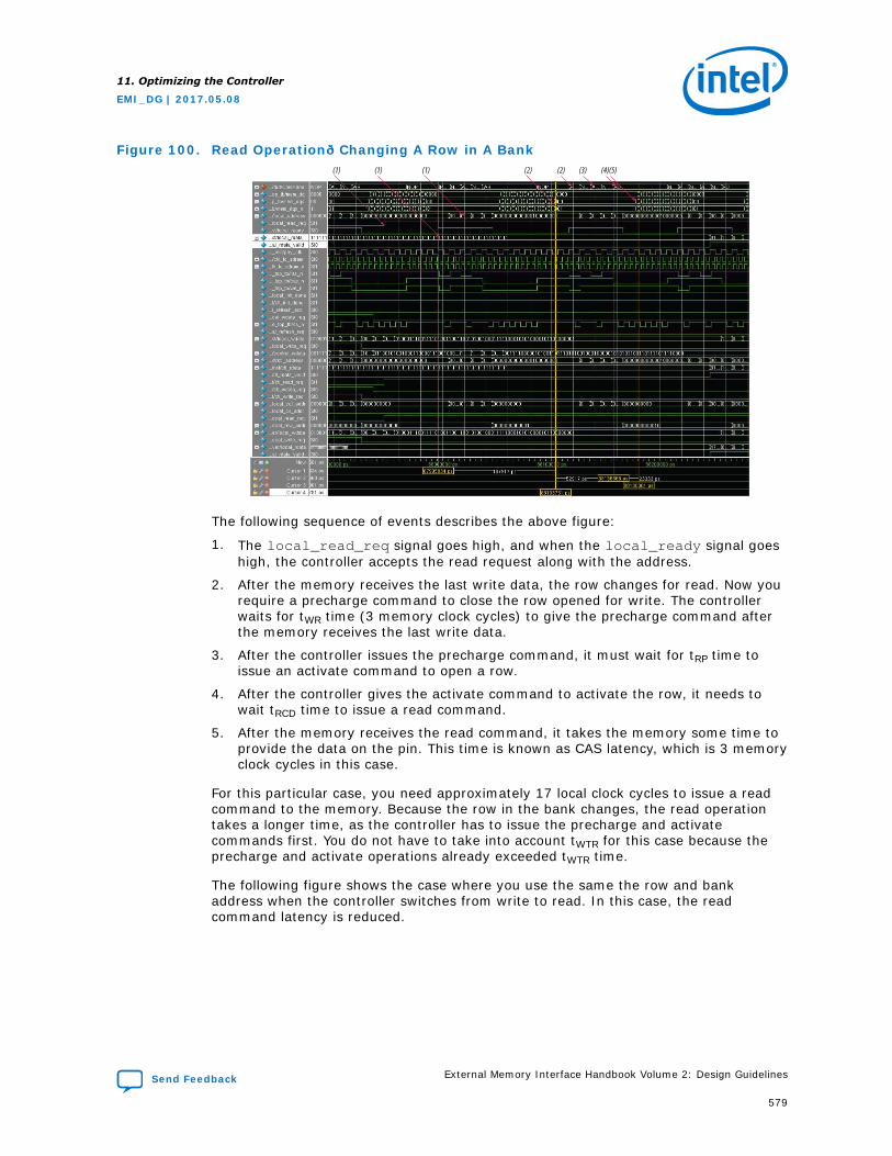
Figure 100. Read Operation—Changing A Row in A Bank(1) (1) (1) (2) (2) (3) (4)(5)
The following sequence of events describes the above figure:
1. The local_read_req signal goes high, and when the local_ready signal goeshigh, the controller accepts the read request along with the address.
2. After the memory receives the last write data, the row changes for read. Now yourequire a precharge command to close the row opened for write. The controllerwaits for tWR time (3 memory clock cycles) to give the precharge command afterthe memory receives the last write data.
3. After the controller issues the precharge command, it must wait for tRP time toissue an activate command to open a row.
4. After the controller gives the activate command to activate the row, it needs towait tRCD time to issue a read command.
5. After the memory receives the read command, it takes the memory some time toprovide the data on the pin. This time is known as CAS latency, which is 3 memoryclock cycles in this case.
For this particular case, you need approximately 17 local clock cycles to issue a readcommand to the memory. Because the row in the bank changes, the read operationtakes a longer time, as the controller has to issue the precharge and activatecommands first. You do not have to take into account tWTR for this case because theprecharge and activate operations already exceeded tWTR time.
The following figure shows the case where you use the same the row and bankaddress when the controller switches from write to read. In this case, the readcommand latency is reduced.
11. Optimizing the Controller
EMI_DG | 2017.05.08
Send Feedback External Memory Interface Handbook Volume 2: Design Guidelines
579
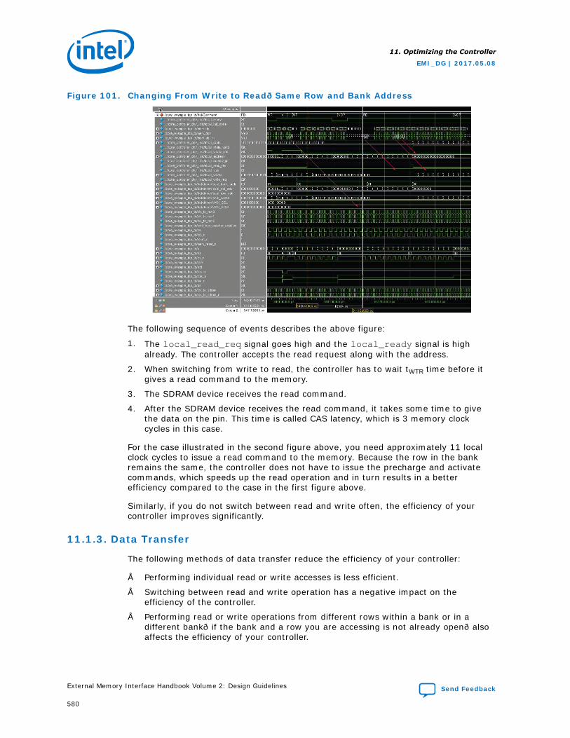
Figure 101. Changing From Write to Read—Same Row and Bank Address
(1) (2) (3)(4)
The following sequence of events describes the above figure:
1. The local_read_req signal goes high and the local_ready signal is highalready. The controller accepts the read request along with the address.
2. When switching from write to read, the controller has to wait tWTR time before itgives a read command to the memory.
3. The SDRAM device receives the read command.
4. After the SDRAM device receives the read command, it takes some time to givethe data on the pin. This time is called CAS latency, which is 3 memory clockcycles in this case.
For the case illustrated in the second figure above, you need approximately 11 localclock cycles to issue a read command to the memory. Because the row in the bankremains the same, the controller does not have to issue the precharge and activatecommands, which speeds up the read operation and in turn results in a betterefficiency compared to the case in the first figure above.
Similarly, if you do not switch between read and write often, the efficiency of yourcontroller improves significantly.
11.1.3. Data Transfer
The following methods of data transfer reduce the efficiency of your controller:
• Performing individual read or write accesses is less efficient.
• Switching between read and write operation has a negative impact on theefficiency of the controller.
• Performing read or write operations from different rows within a bank or in adifferent bank—if the bank and a row you are accessing is not already open—alsoaffects the efficiency of your controller.
11. Optimizing the Controller
EMI_DG | 2017.05.08
External Memory Interface Handbook Volume 2: Design Guidelines Send Feedback
580
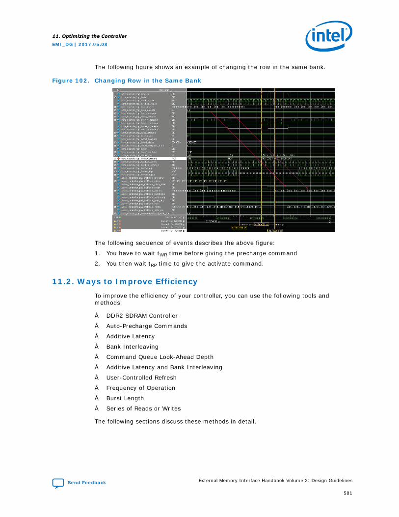
The following figure shows an example of changing the row in the same bank.
Figure 102. Changing Row in the Same Bank
(1) (2)
The following sequence of events describes the above figure:
1. You have to wait tWR time before giving the precharge command
2. You then wait tRP time to give the activate command.
11.2. Ways to Improve Efficiency
To improve the efficiency of your controller, you can use the following tools andmethods:
• DDR2 SDRAM Controller
• Auto-Precharge Commands
• Additive Latency
• Bank Interleaving
• Command Queue Look-Ahead Depth
• Additive Latency and Bank Interleaving
• User-Controlled Refresh
• Frequency of Operation
• Burst Length
• Series of Reads or Writes
The following sections discuss these methods in detail.
11. Optimizing the Controller
EMI_DG | 2017.05.08
Send Feedback External Memory Interface Handbook Volume 2: Design Guidelines
581
11.2.1. DDR2 SDRAM Controller
The DDR2 SDRAM controller maintains up to eight open banks; one row in each bankis open at a time.
Maintaining more banks at one time helps avoid bank management commands.Ensure that you do not change a row in a bank frequently, because changing the rowin a bank causes the bank to close and reopen to open another row in that bank.
11.2.2. Auto-Precharge Commands
The auto-precharge read and write commands allow you to indicate to the memorydevice that a given read or write command is the last access to the currently openedrow.
The memory device automatically closes or auto-precharges the page that is currentlybeing accessed, so that the next access to the same bank is faster. The Auto-Precharge command is useful when you want to perform fast random memoryaccesses.
The Timer Bank Pool (TBP) block supports the dynamic page policy, where dependingon user input on local autoprecharge input would keep a page open or close. In aclosed-page policy, a page is always closed after it is accessed with auto-prechargecommand. When the data pattern consists of repeated reads or writes to addressesnot within the same page, the optimal system achieves the maximum efficiencyallowed by continuous page miss limited access. Efficiency losses are limited to thoseassociated with activating and refreshing. An efficiency of 10-20% should be expectedfor this closed-page policy.
In an open-page policy, the page remains open after it is accessed for incomingcommands. When the data pattern consists of repeated reads or writes to sequentialaddresses within the same page, the optimal system can achieve 100% efficiency forpage-open transactions (ignoring the effects of periodic refreshes, which typicallyconsume around 2-3% of total efficiency), with minimum latency for highest prioritysingle transactions.
If you turn on Enable Auto-Precharge Control, you can instruct the controller toissue an autoprecharge read or write command. The next time you access that bank,the access will be faster because the controller does not have to precharge the bankbefore activating the row that you want to access.
The controller-derived autoprecharge logic evaluates the pending commands in thecommand buffer and determines the most efficient autoprecharge operation toperform. The autoprecharge logic can reorder commands if necessary. When all TBPare occupied due to tracking an open page, TBP uses a scheme called on-demandflush, where it stops tracking a page to create space for an incoming command.
The following figure compares auto-precharge with and without look-ahead support.
11. Optimizing the Controller
EMI_DG | 2017.05.08
External Memory Interface Handbook Volume 2: Design Guidelines Send Feedback
582
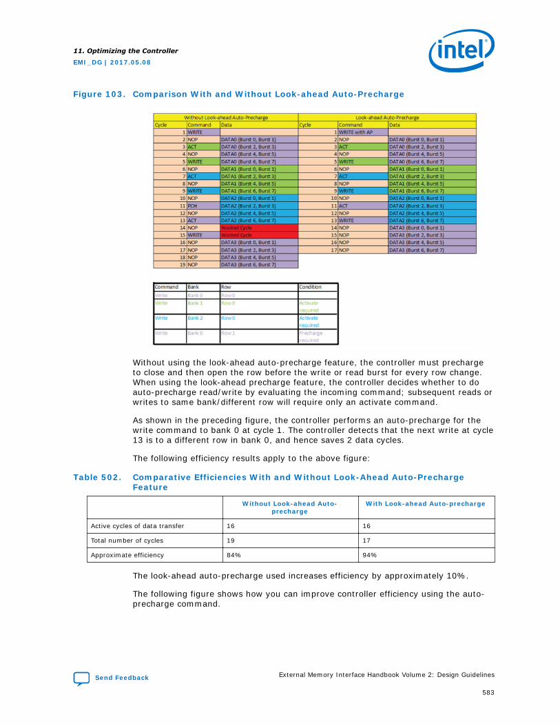
Figure 103. Comparison With and Without Look-ahead Auto-Precharge
Without using the look-ahead auto-precharge feature, the controller must prechargeto close and then open the row before the write or read burst for every row change.When using the look-ahead precharge feature, the controller decides whether to doauto-precharge read/write by evaluating the incoming command; subsequent reads orwrites to same bank/different row will require only an activate command.
As shown in the preceding figure, the controller performs an auto-precharge for thewrite command to bank 0 at cycle 1. The controller detects that the next write at cycle13 is to a different row in bank 0, and hence saves 2 data cycles.
The following efficiency results apply to the above figure:
Table 502. Comparative Efficiencies With and Without Look-Ahead Auto-PrechargeFeature
Without Look-ahead Auto-precharge
With Look-ahead Auto-precharge
Active cycles of data transfer 16 16
Total number of cycles 19 17
Approximate efficiency 84% 94%
The look-ahead auto-precharge used increases efficiency by approximately 10%.
The following figure shows how you can improve controller efficiency using the auto-precharge command.
11. Optimizing the Controller
EMI_DG | 2017.05.08
Send Feedback External Memory Interface Handbook Volume 2: Design Guidelines
583
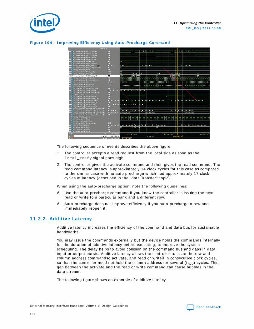
Figure 104. Improving Efficiency Using Auto-Precharge Command
(1) (2)
The following sequence of events describes the above figure:
1. The controller accepts a read request from the local side as soon as thelocal_ready signal goes high.
2. The controller gives the activate command and then gives the read command. Theread command latency is approximately 14 clock cycles for this case as comparedto the similar case with no auto precharge which had approximately 17 clockcycles of latency (described in the "data Transfer" topic).
When using the auto-precharge option, note the following guidelines:
• Use the auto-precharge command if you know the controller is issuing the nextread or write to a particular bank and a different row.
• Auto-precharge does not improve efficiency if you auto-precharge a row andimmediately reopen it.
11.2.3. Additive Latency
Additive latency increases the efficiency of the command and data bus for sustainablebandwidths.
You may issue the commands externally but the device holds the commands internallyfor the duration of additive latency before executing, to improve the systemscheduling. The delay helps to avoid collision on the command bus and gaps in datainput or output bursts. Additive latency allows the controller to issue the row andcolumn address commands—activate, and read or write—in consecutive clock cycles,so that the controller need not hold the column address for several (tRCD) cycles. Thisgap between the activate and the read or write command can cause bubbles in thedata stream.
The following figure shows an example of additive latency.
11. Optimizing the Controller
EMI_DG | 2017.05.08
External Memory Interface Handbook Volume 2: Design Guidelines Send Feedback
584
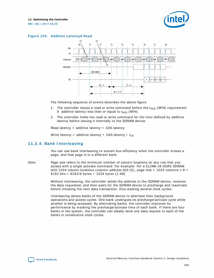
Figure 105. Additive Latency—Read
CK
Command
DQ
DQS/DQS#
T0
[1] [2]
T1 T2 T3 T4 T5 T6 T7 T8
CK#
tRCD (MIN)
ACT n
n n + 1 n + 2 n + 3
n NOP NOP NOP NOP NOP NOP NOPRD
AL = 2
RL = 5 (1)
CL = 3
The following sequence of events describes the above figure:
1. The controller issues a read or write command before the tRCD (MIN) requirement— additive latency less than or equal to tRCD (MIN).
2. The controller holds the read or write command for the time defined by additivelatency before issuing it internally to the SDRAM device.
Read latency = additive latency + CAS latency
Write latency = additive latency + CAS latency – tCK
11.2.4. Bank Interleaving
You can use bank interleaving to sustain bus efficiency when the controller misses apage, and that page is in a different bank.
Note: Page size refers to the minimum number of column locations on any row that youaccess with a single activate command. For example: For a 512Mb x8 DDR3 SDRAMwith 1024 column locations (column address A[9:0]), page size = 1024 columns x 8 =8192 bits = 8192/8 bytes = 1024 bytes (1 KB)
Without interleaving, the controller sends the address to the SDRAM device, receivesthe data requested, and then waits for the SDRAM device to precharge and reactivatebefore initiating the next data transaction, thus wasting several clock cycles.
Interleaving allows banks of the SDRAM device to alternate their backgroundoperations and access cycles. One bank undergoes its precharge/activate cycle whileanother is being accessed. By alternating banks, the controller improves itsperformance by masking the precharge/activate time of each bank. If there are fourbanks in the system, the controller can ideally send one data request to each of thebanks in consecutive clock cycles.
11. Optimizing the Controller
EMI_DG | 2017.05.08
Send Feedback External Memory Interface Handbook Volume 2: Design Guidelines
585
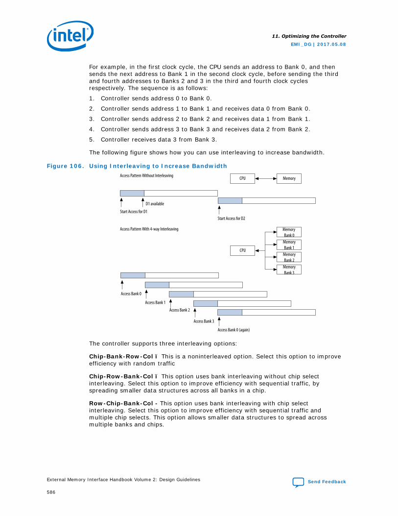
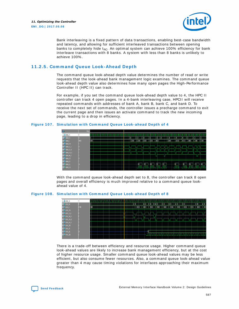
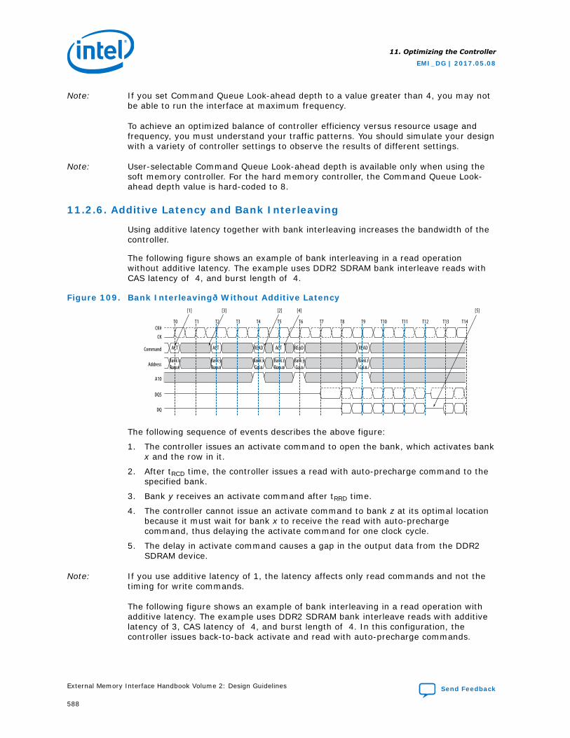
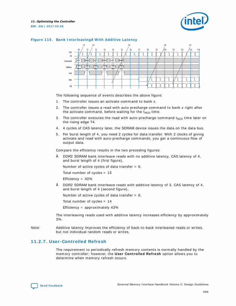
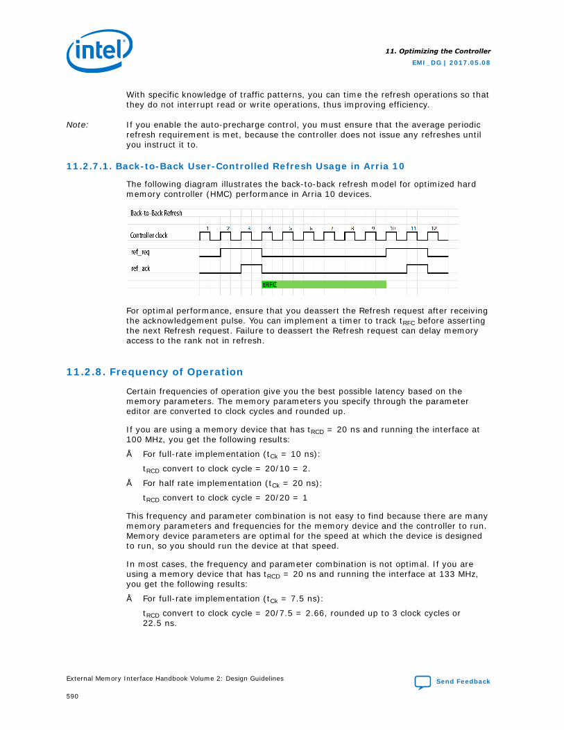
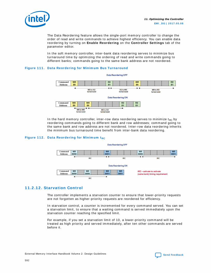
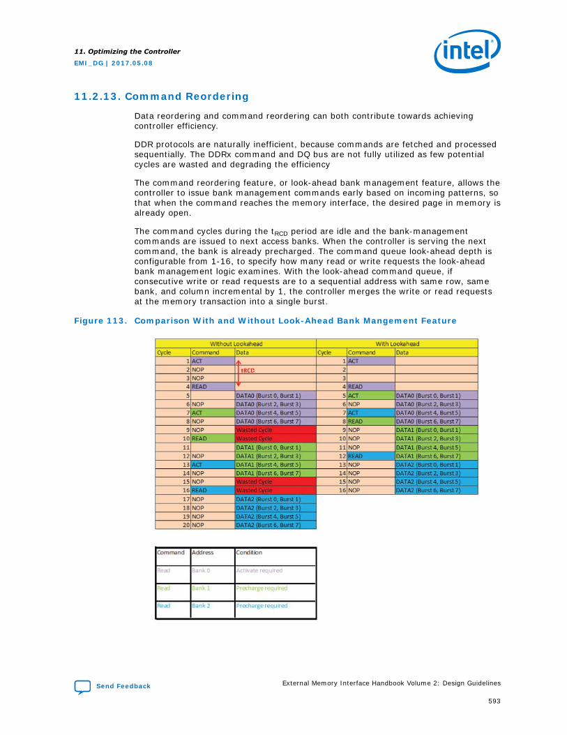
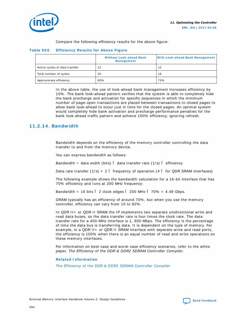
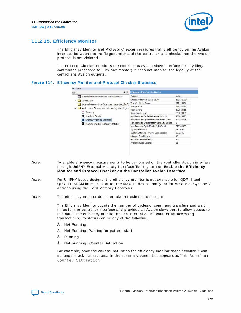
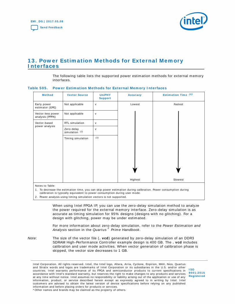


![Volume 1 Issue 24 June 2017 (twu 2017 - Varanasinnvns.org/download/enews1.pdf · 2017-07-17 · uxj vk;qDr Jh jes'k pUnz flag la;qDr uxj vk;qDr Jh lanhi JhokLro dksvkfMZusVj] dEI;wVj](https://static.documents.pub/doc/80x56/5e7de60dd696bc51877758d4/volume-1-issue-24-june-2017-twu-2017-2017-07-17-uxj-vkqdr-jh-jesk-punz-flag.jpg)


