AD-A252 817 QL% ttaW Ranc end Gem'akny MTT Chiplm. .'A. CNR, Italy NEIFrance ~*A~k~p~u Rdserch Off ice UK IEEE Microwave Theory and Technkqu Society W.- . Approved for ptubl 101dam 92 710 02 86
Transcript
AD-A252 817
QL% ttaW Ranc end Gem'akny MTT Chiplm.
.'A.
CNR, ItalyNEIFrance
~*A~k~p~u Rdserch Off ice UKIEEE Microwave Theory and Technkqu Society
W.- .
Approved for ptubl 101dam
92 710 02 86
Technical Program CommitteeP. Lampariello, University of Rome La Sapienza, Workshop Co-ChairmanR. Sorrentino, University of Perugia, Workshop Co-ChairmanV. Fouad-Hanna, CNET, FranceH. L. Hartnagel, Technische Hochschule, Darmstadt, Germany
Orgpuizing- Committe
Rl. Giorgini, Itelco S.p.a.V., Alleva, Itelco S.p.a.S. Monelli, Itelco S.p.a.S. Catena, University of Perugia
SecretariatN V. Ppni, University of- Perugia .
L. Castellani, University of PerugiaC. Paolotti, University of Rome "La Sapienza"
DISCLIMEl NOTICE
THIS DOCUMENT IS BEST
QUALITY AVAILABLE. THE COPY
FURNISHED TO DTIC CONTAINED
A SIGNIFICANT NUMBER OF
PAGES WHICH DO NOT
REPRODUCE LEGIBLY.
Microwave Theoy and Techniqures GocielyC.&G. Italy. Franco and Germany MTT Chaplets
1992 International Workshopon Millimeter Waves
April 22.24, 1992
I'.II.14ZEI del Capillano del l'opolo
Orvieto, Italy
Orcginimcl bX:
Central aind South Ihlily MIT ChapterFrancex mrr n:iaipir
S. MOn)Cil, h1clco S.p.a. I acnuelS. Catcnma, University tif P1cruri.i Jt r fi*t on
Secrewarlt 1 Distribetioalf
V. Papiaai, Univcsity of Pecrugia IAvllabilitY Cod ej
L. Calelai, Universiity of I'crugia I A.1adOC. hi'ololii, Uaaiver.%ily of R(omei "LaI Sipicaai;'ts SPec
FOREXA'ORD
Wclcottic Lo thirdcdtitlfilte Itieniattital wavi kshi p o Nlilleter 'Wave.%. licing heldat lte
I'ahjazz.hid Capot, Ie 1'ojvIh lin Orvielt. Alter lte elithitaragij; succe,'ichth pie vetus cditiiiis at
tlie Uniiversiy 44, Rouiteir Vctgati" in IM ;tolad at the Ujniversit y tit- Iertigia in 1I ' it wasidecidled it) or1galize a necw vwikshii.l, a. a comv.lii i.4.1 lx-te*Il Olw ( eitti1.s t1 iS.11il1 Itily (' lcalitrwith the Framie l e tayCt~t i~site IhLNjtwv 'tiL uh chii~isSwey
111C city oif Oricto has beenl chttiscr a~s lte venue I, it- tisi.vt nott simtply beccause it i. icatedmtidway bctiwcn Ittili and P'erugia. but mintly hIr its tunique cltrtit due lt its sugvestlivc mnedieval
aptpearattcc and thc rich artistic patriimiy dalizig luck (it lte Elrutinsci peinid. Thle l'alaz, del
Capitano del liopolo is nlo do)ubt anl cxtraordiiay cmotiatim, betveeti a litylorical mcdievoal pohiizza
and a niudenti atnd Cfficient Cotugm-ss Ccnter.ITELCO S.p.a. Clitusiastically agrecd to sponsoo~r thic wolrk.shop alld bas beenl a fuiidamnuttal partinerini the torgatniJatiii. 1w sticial lirutram is alsti very attractive. mtcludisie a very itice conceit tit twit
Canadian artists. Tr. Goudic arid D. Lawtiott.
Wc would like ito thank all lte invited specaker.- whit kitndly agreed lt participatc ii the
workshopi and the miany otlters who have woied for its 'necess. Wc are deeply graut lt 'sts
Carrara, onc ul' the fiihaers oaf tuicrtiwavcs in Italy. wtim accepted oiur invitation toi welcomi lte
participanits at t01C q~1iipentig C55iil.
I'aulo Lati~mrihlm, antd Roberto Norcutinlo
%Vurksltnp Co.Chaiiraicii
it. r~icieteI. Akoidoneter. lave Aloplici~nont% joid IriTehnhojgy 'gid
K. Crueller. it Net, Passiive A-ier,,i*,a,' Sciner for Airjvtprior Aleavisritwit t of Itlariti #il IauIinus
NI. Aikawn. AIMIC Tecitiinlogy for ConmFuieatini Sysrtms
It. IFunck. New Integrated SubsYmestm fopr llntgrlatAtpiiins
D. Po,rn New Alilhimneter-110a,'e Devices: Realezatiint tand Perfoyrntie
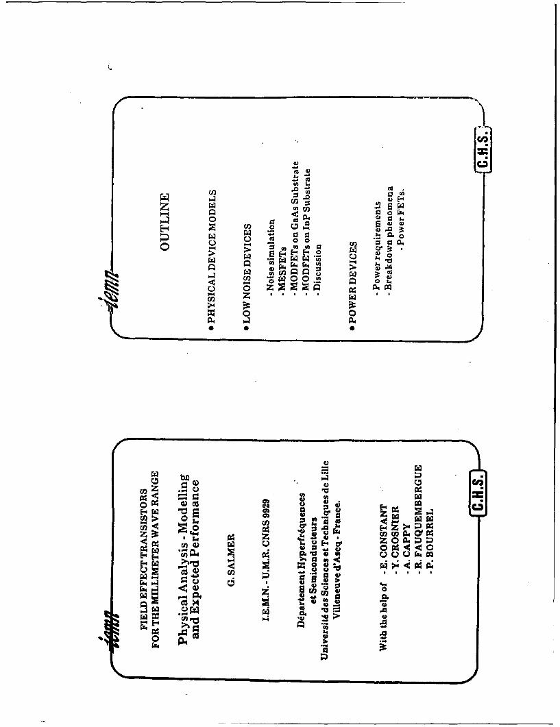
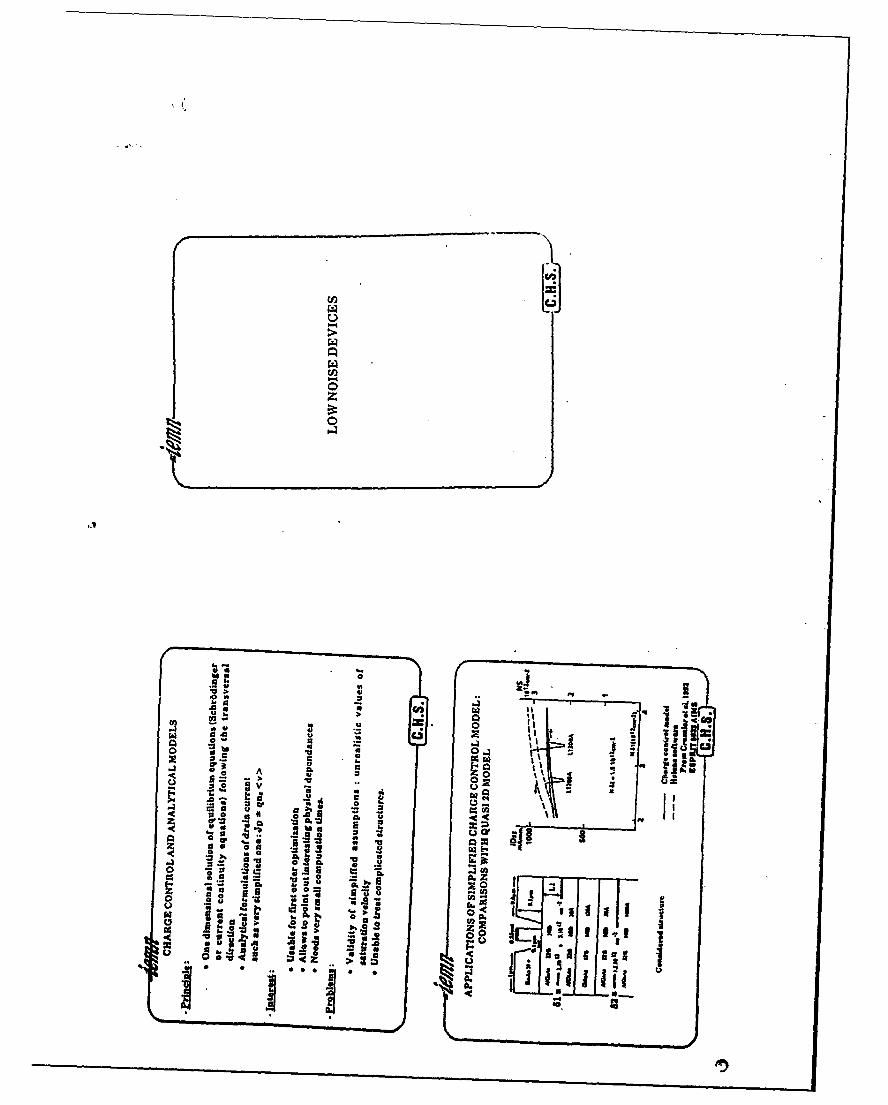
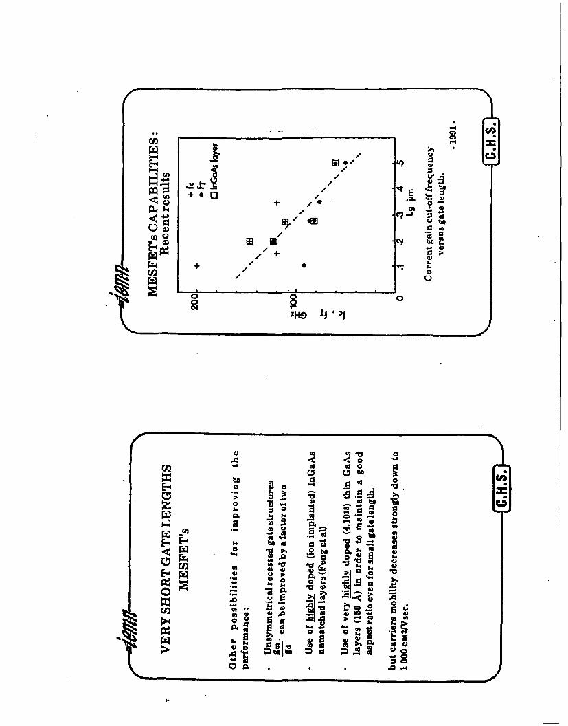
G. Silancr, FiclEffect, Trimoittfo firsfr the ,thihi,,eter. Wuter Range: 'hiYsieal Atoodv~js. Alawlelutj' UlLtImcceml I'eqrune
J. Frcyer. Tims-Tertninual Millimneter- lVaer, Deces~
1I. L. I Ilrttutgel. 'lechioh,gy Iee ,onrlim. 1o'i,,r-tvu ,Vu,,i-,n Vrowtue.%
T. ltoht. O1164:111 Cmntrol 1fillinmler4Vtlatri Circuits
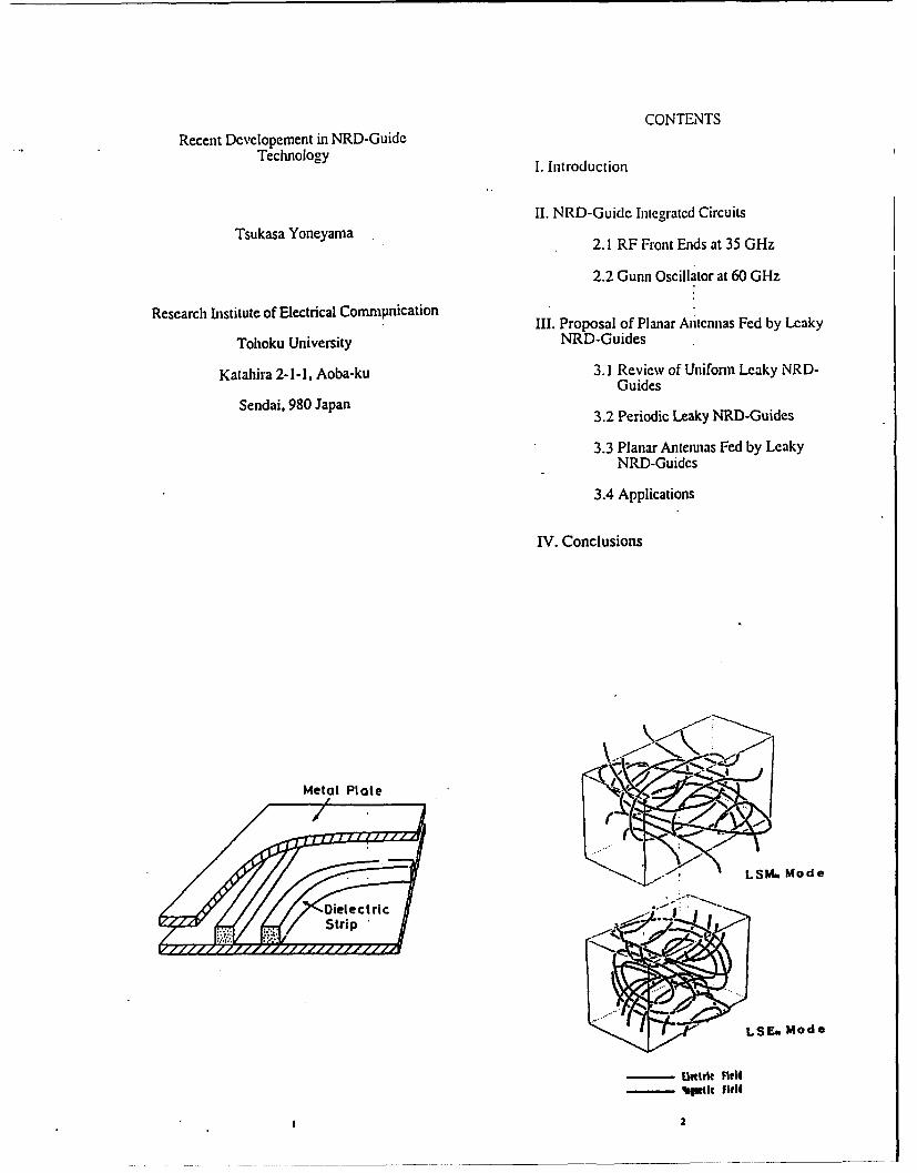
T. Yotwymatiat. Receott IDeehotnns. #of NRI)-;,.,s. Te, impIig
It. 11. Jamset. Adv'anced Design Tee hnu jues fir Leiear adS Nonldinear MAIC's intto lie Atillimleter. WarrRegimon
V. Fi~uad I lanita. CAD) of Millimter. Wa~ve P'assive Cemioments its Siupended Alicratip Techonahegy
A. A. Ohmer Leakage and Crastalk lFffects in Alilimeter-lMaw Integrated Circuits
N. Alemupitius. JD Ainodeling lof Atidhi neter-Wov Circits unitd Anmismnn
Ouasi-opt~~~~~~~scher98 Toyotau MeM 60icua 6nd 86Gil---------------------------aVS
+~uis DetsheAeosac
Millim tve te1olg issa maur today
oTralgidn ce systemsiaiF0Tolisio avoidane simlfesorse
for8 highip rate production,
hybnwrird and mooShT are avilbe n
+ rotscpe Aroucenhsbenluce
hilmeeave aie hnmomentum atroa
ovr cT-ommuraficatinfosyatimsoLAN radios(CMS
aremal gdrivnce stm
Co c lision aviac se or
c.~ u - 690010cc .80 v-.'D i E
'44w !' CC Ut
C4 4 c~ 'o c -
r , 2:1 4' -p .ulo u, !g i ~~l o 9 . QZ O c .6
m. 40 04 t lc un E: ;; ,
mcoso (Z Cf. E U L
4 - cii cr.3S aE!( )
1Z .4.sU4 Z . -D
un~~' '(S -61 v
-h~ 0 1: F -1 .V:9-n m U" -4m .a..Ec u L
0 1. m 2L ' 2 u S u4 8 ... '
CSZ T r. r. 'D, ,
m o 6 .. E u IDc cu. c 2 t
6 - A.~
"A i~' m- 112
xE5 8. EEO
10 Z, c y; E
,c - . 11
410 r
a k~ cj
go a,
-22 -b ,MgO.,
Z; M. E 9C
.2 Zz
.2~& 6T ~- j.
F 15"E.
L0 EE S!~0. ~
- P. 1
-a D;; ,
3 C)
-0 2 A yp g
cu Le .04- 0.'
-Z,)A .9>
-13~MI 5, JCf2Cf
- -s L" ..)L*1 r
&C
Z~ .'Q .C . . .U . .. e~7 -
v&:g - iD at ZZ
.0 c ar o ,0~ !,- O" 4 Q 'C "1 ,,o*
r ..
Z- 'ZIL,
13a. 0- o coQ E Q ' ' Z'o. mC 4, c, w~ S. V F, 0t 0
-00 : Q'j a- c'~'Ca4. , -, 4& z ~ - 5. ".
C9 T) E t-b w--42CC U00c
wD~ 7a 9l E 4 Z
f0 4 3a . C 2 w 5. MESn-3 1-cC .6 0 E . -c o' 9 ; Z. U=~~~~~~~ CCE 0G~. zm~~0~ a
z~w~m 1 c E .-
!> cA - , - Ic
- 06
q WE Z1, M C- rae3 Z
cc .0 ZQ 4
CL m 0~ Cw ~ ~ ~ ~ -* a -c .; -c
cc E ckm y m ;i 8 o ica c. -
-9 E & cf.~c~ ' owe 2" u w
k - C c 1 E, - "''0FC A T V w 1. f! . u
ogi w. .900 SEO D w 'w L i zf L
zscu~" u~j e- ,w(c-> X6 -o2
A NEW PASSIVE MICROWAVE SCANNER FOR
AIRBORNE MEASUREMENTS OF MARITIM OIL
POLLUTIONS
K. Cruener
DLR, Obcrpfaffcnhofen - Germany
A New Passivel-Ncrpwave Linescannerfor Airborne Measurements of Maritime Oil Pollutions
K. Griner, G. Kahlisch, H. Schreiber, P. Sliwinski* B. Vowinkel
German Aerospace Research Establishment (DLR), Oberpfaffenhofen,FRG* University of Cologne, Cologne,FRG
Abstract opcratcd optical and active microwave scusors in parallelto a multitudc of microwavc radiomcters (iinescanncrs
Ancwpassivemicrowavclincscanncr has bccn developcd and profilcrs). The gcneral aim of these cxerscs was tothat will be used for airborne operational mcasurcmcnts cstablish specifications for an improved operational scn-of maritime oil pollutions. Thc systcem consists of two sor package for quantitative rcgistration of oil pollutionoffset rotating parabolic mirrors and two radiometer scts, at sca undcr nearly all-weathcr conditions.where each set contains threc radiomcters at 18.7, 36.5 In 1989, the German Ministry ofTraffic decided, to realizeand89GHzc enn qucucy.A ftLhcr89GHzradiomc- a new maritimc surveillance system on board a moderntLrisusedforthcmeasurementofthcaveragcradiomctric Do228 aircraft [4]. In addition to improved scnsors util-sky tmeip ture. Th system is ontinuousy calibrated by ized up to this time in the first gcocration aircraft, thc new
'the use of a "hot load' at ambient tcmpecratur and a system will include newly developed sensors, a LaserpClticr cooled 'cold load". A computer system allows Fluorosensor and a multiple frequency microwaveonline data reduction for the estimation of the amount of radiometer which allow a morc thorough analysis of oiloil on the sea surface. spills. This includes a quantification of the spilled volume
over a range covering small discharges up to accidcntalevent% and the classificatiou of oiltypes.
L IntroductionIL The New Radliomder
Pollution of the sea has increased up to levels which cafaresult in severe risks for the marine ecosystem. High loads A. Rcquirtnentsof oil have been observed in many coastal wates. Inaddition to the procurement of'oil combating ips', this Th Archimd exercises offered a unique chance tosituation has led to the demand for airborne sureying studyradiomctcroutputsinthe5GHzto90GHzrange formethods for providing helpful data for oil spill dcan-up different types of oil and oilwater emuisions of varyingoperations following accidental discharges, and to moni- thickness (up to several millimet r) during a variety oftor the legal aspects of per.mat ontributions to an- realitic environmental condatiom A series of findingstime W oltos resulted which, together with some operational restraintsIn Europe, aircraft equipped with remote scsing instru- are now forming the basis for the development of the newmeats haw been provided in various countries in the radiometer.Indetail, basicrcquirmcntsforaradiometerperod 1983-19M8 for a regular survey of coastal waters of second generation armand, in view Of a sCMor systcm of second generation, for - sie. ous mcasurcmcts at several frequencies tothe purpoe of basic research. Since 196, for example, avoid ambiguity problems during the determination oftwo Dornier Do28 aircralts equipped with an IRAW laye tickness and, above all, the oil volume; an errorLi.acanner, a Side Lok in Airborne Radar (SLAR) of volume estimation smaller than 5D% is tolerated,and a scanning 35GHZ-Radiomcr have been flown inthe German- rspoombtareas of th North Sea and the - selectin of frequency bands with reference to possiblcBaltkic Sea, aiming at a coatinuous surveillance of mari- interferceces due to man-made noise and regitrationtime pollution and an improved guidance of oil combat- of oillayer thickness in the 50#m to 3mm range,ting operations. In 1983,1985 and 1988, under thesponsorhip of the European Community, a seris of - simumanous regstration of the sky radiation at leastinternational airborne cxerciscs took place in the North at the highest fr quency band which is the most seasi-Sea (Archimedes Campaigus [1-3D. Different institutions tivcou with respect to variatin oafwcathr conditions,
MS 199 EEEMTS tmalh l b wa Sympoumn. Jun 14,1992 Afaquuqus * Nw Mxico. USA
2
- a scan angle as large as possible to realize wide scan In general, for optimum data evaluation, the sky radiationwidths. which influences the linescanner "uput should also I-
- aspaialresluton s hghas ossbleundr te po- constandymapped with a separte sytem in all frequent.Vis a f sptiaesltn m aim asoposable ndcnsr the o bands. But for simplification and cost reduction only oneraioofetemamu toer abcagleegh:8m dmins(r h furtherC9Hz radiometer with a fixed sector-horn anten-
radlmetr pckag (lngt:88zn, idt:S~m),na has been designed for the sky radiation measurement.- consideration of typical flight altitudes of 300m to Its output delivers a mean-value of the relevant sky radia-
1000 an air.;d veocites ear 0m/. ton which is the optimum basis for numerical estimation100G an ai~af veociiesnea 7O~s.Of the corresponding values at 36.5 and M&7 GHz. TheIL Feuncy Ranges errors resulting from that procedure are expected to be
smaller than 5D%.All requirements, listed above, have been considered-during the development of the new radiometer. 7%e cJDJmP C. The Scanning Principlestruction Of the linesanne was achieved with a compactconfiguration that realime simultaneous imaging at M, Scanning happens with the aid of two parabolic mirrors36-5 an 9 .M rqec ad eetdaer-. installed in a continuously rotating cylinder (Fg2). Bey-
anrvd 8or z Thsie eunc y barnds sethe Ariede- ond both front sides of the cylinder, identical thre-chan-campaigns, measurements at 17GHz regularly resuilted i nel-receivers are placed which are coupled to thethe best volume estimations for thicker layers. A parabolic mirrors via plane reflectors and through holesfrequency around 35GHz seems to be the best com- at the front sides. This scanning principle should be par-Promise with respect to geometrical resolution and bad ticularly advantageous with respect to operational use. itweather capability. 90GHz images are highly resolved and avid osiltn oeet f h anrfetrcomparable in quality to IR images (ig. 1). A sensitivity rttoa wthsad-urnesrdumei hdown to a layer thickness of 5qum exists. Oil-in-water case of a failure of receiver channels. Further it supportsemulion and white caps (false alarm) can be determined a simple method for cmontnuu calibration. A swathqualitatively well in thi freqcy rage widt of 476m is achieved for an ahitudeo30m (O=t).
291 26 01t D
107 1 3 30 362 1Fg L Example for the representation of passive micro- Fg. 2. perspective representation of the MWR coaLigo-
wave oil Spill measurements. Oil slick taken at ratio. developedL To parabolic reflectors in a90GTU during nigh time together with volume rotating cylinder and two receiver Xp- realmestimations (liter); altitude 4000 ft. scan width two scaines per revolutIn Thermal hotlol440.m, mxium variation of brightness sources are used for a onslamam cajibratiom.temperature 21 IL
D. The Calibratlon Principle E. Receiver Front- and Back-End Characteristics
ThU cal~bration of the radiometer output signals is done To realrm optimum radionietric resolution tota powerby using a hot load at ambient temperature and a pchticr- and hetcrodync principles are applied to all channels.cooled cold load. The hot load consists of a sheet of Balanced mizcrs arc used throughout. They show thcabsorbing material that is mounted on the inner wall of lowest noise; figures which arc, presently, obtainable withthe radiometcr main rack. As the effectivesarea of the cold commercial devices at room temperature. The receiverload is mauch smaller, a further mirror is used for focussing housings shown in Fig.2 only contain the sin*i front-endthe beams of the rotating antennas onto the cold load. modules which can be simply removed like a drawer forDuring each revolution of the cylinder a complete series better access during repair. Ilc adjustment of a singleof hot/cold mecasurements for all frequency channels is radiometer channel for calibration happens by the usc ofaccomplished. a variable offset amplifier which is placed in a seperateA cross sectional view of the cold load is shown in Fig. 3. back-end housing, Low pass filtering and AID conversionThe absorber is cooled by a 3-stage Peltier element that follow after low frequency amplificaion.has a power consumption of 45W, this results in a The whole radiometer system is completely computertemperature difference of 51K with reference to the case controlled. Not only calibratioir is done automatically buttemperature. The core of the cooled absorber is made of also a system configuration on the basis of a priority listaluminum in order to get a nearly constant temperature (after switching on the radiometer). Further, during thedistribution up to the tips of the pyramids. The surface is measurements, a numerical correction of the antennacovered with a layer of absorbing material. The reflecting beamn squint angels which result from the displacement ofinn"r wall of the load case has a conical shape resulting in the feedliorns is realized. Digital processing, in addition,an incmed effective area of the cold load. This is impor- allows a continuous observation of the operational condi-tant for the 18GHz channels which have the largest beam tions of the system by monitoring and storing data such aswaist that is also somewhat off axis. The space between the physical temperatures of the housings and calibrationthe; inner wall of the case and th cold load is filled with loads, the noise fiue of the front-ends, and the gain andsmall balls of expanded polystercne in order to prevent offset voltagos of the variable amplifiers. Finally, in theconvect=o of the surrounding air and condensation of case of oil spill measurements, layrthickncss and volumewater. The overall efficiency of the cold load has been is directly processed from the received signals.datrminedwith anexltmal coldload consistingof alarge Different spatial resolutions awe obtained for the single,sheet of absorbing material cooled with liquid nitrogen, frequency bands by optimum utilization of the antenna
apertures especially at 89GHz. However an identical res-olution which would be important for an automatic un-
LMambiguous estimation of t olume could be achievedaueicly
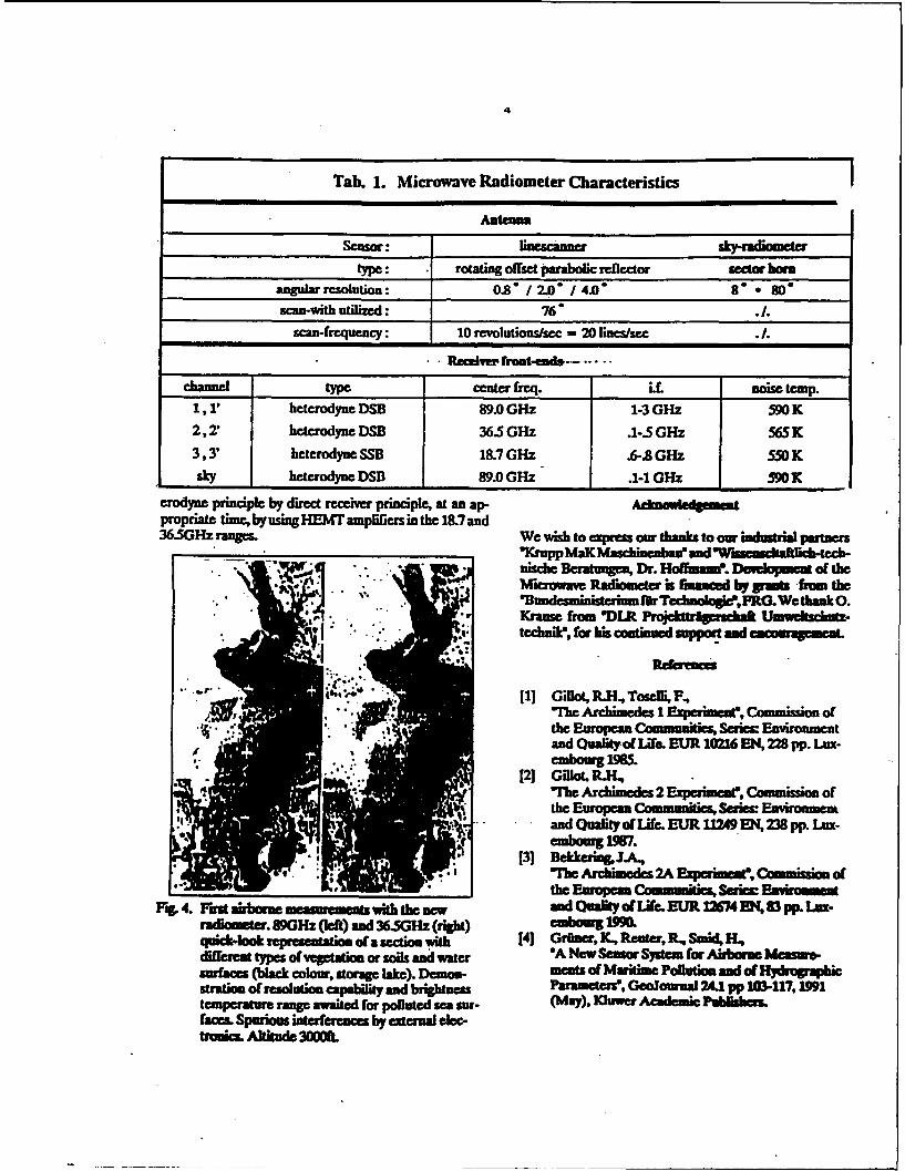
..... ... 5In table 1, the most important radiometer characteristicsPUT DewT 0~:~aa 0 u,0v0 -we listed.
ilL FIrst Mrbarm Masuncmn
00 40O UTTM After itctmion and installation intotheaircraft, the new
. 00000::: systcm bbm Gumfor te frtim inNovember M99
tom had beendveoe for imag representation, toqualify the radiometer. The first rendis showed that theconcept of the now systemn wors vary well and that theresolutaonsmcetspeafled vales(l'ig4).Ontheother
Fag, 3. hand, a depranalysis revealed some spursuos interfr-FW 3 Prncial cnfiuraionof te cM lacs, among other thinp, due to local-oscillator radia-
tion in te M87 and 36.5GEz ranges These problemThe sky-radiometer is calibrated by the same Principle, arise from the absecm or unilines at the receiver inputsHowever here we arm using waveguide ferrite switches to which normally results in higher senitivities for well ad-switch the radiometer input to the loads. The cold load Justed devices. In view of the first measurements aboveconsists of a Waveguide absorber that is also cooled by a oilpolluted sea that are shedulded for April 1992, addi-3-stag etier elementI. tional filtering in the 18.7GHz chianuels will be a short
term solution. It is planned, however, to replace the het-
erodyne principle by direct receiver principle, at an ap- qdcngwledmeMtpropriate tiznecby using HEMT amplifiers in the 187and3CI5Gz ranges. We wishtopi eres our thanks to or iodstrial partun
*Krupp MaK Raschineaieu and %Wiseaudlhaftllda-tech-nische Beratungen, Dr. Hoffin". Developmnent of theWmrawave Radiometer is fianced by prut from the
e~~mn~ruflkrTechgeFRG.Wethak 0.
technik, for his continued mappart andip 4M--ESQa-e
straion resluton cpabiityand righnes ~ Oualiy Gof ouife. ER1249 R pp S 2 M-1 Lux1
temeraur rageawate fo plluedseasu- (he Archiede Ad ei Commision ofaces.he Spurious interference byes extenal AM
MMIC TECHNOLOGY F OR COMMUNCATION SYSTEMS
M. Aikawa
NTT *Japan
-00
(1)
(j-o -a c-
ci) ci) ; (1)0 =n 0
cu a) 0a) > _ C 0
C- c0 (1)U>, 0 I
a-) U)M> 2() W i U)
0_ 0cuE~i 0' I;
]0 0l (f (IMZ,~ Mr (1) 2? c
CL u W' 0 166 6c
(v a) n cun o.0)0 m-C C)
(i0 Q- CU1c n < cii
1 ) .- .- -
C-d
Cd)
ci) S)C)U0 c
0c 6? c
00
0) ! .9 CCE~* ' to0
Ii ' i; " '(.-0 -C InU
o 0 0
0) 0: 0) 0
C vL
C) Z c r o2 1
0 o-C -'2 0
01
o C,
In
60 w U
z rA u) LU l gu
IL 0usU
LL U)(GP) SSOI N~fl3U
C,))U))
-' z< 2)
zz
> 40 z
- z 0
w a)
f-E. CL C)ww0) z E
I-IX
mc (r00C
w0a
0CL
ELL
4:!E' -I
0 L
* 0
CLa
0U)
U)
E
U) .76
C) I
AA
IIL
M ~Q)_zco 8-~0~~ihLLii I i
C\J NV w
E C.)
z 2U 0 E L-z - I]~J
-Z 1 3 E 0 n
WL E E 0-
to IzD~ C/
6 - 0 vU
Lu 0) W LAL
09 .- C) 6 uU) (Up SSO N-OI.Laa) SN>
HO cc .- LnELoa3. LA>
10DDL a l C,
C- C) C
2 y U -
U)(ww-p) ssoi
-0 ) 7Ko EE
Cr U)C) )< 4
5 ) 0 Z.0 c00 -im .6 cc~.
C) z
uI Lu
U- 0CU _
oo D -Z~
09P NOI.LV1OSIo
-7)
U)
0~~ , 0 aC
OD F)
0) to
0)0
LL CM 5
M m 0 n0- - - -
0
LL~
~Ul
U)U
N~~ CC0)~
I 0
C:
N Ua) a)
a))
(Dn
oCC00
La C 0
w zO
-o)Ow a)
W E))
a)U
-< a)>c: >(B cu
00
z SE
N1~l C4- ..
W (0-
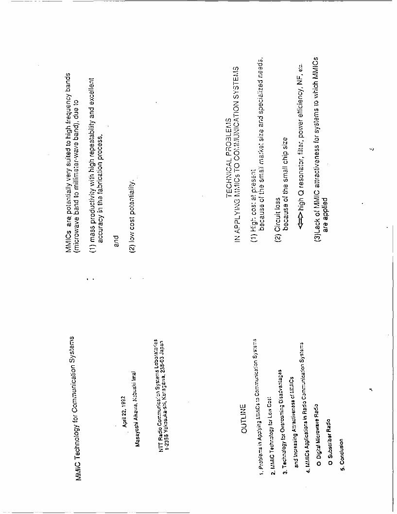
Prospects for MMIC Applications in the Communication Field
MMIC MARKET SIZE
(1) MMICs are now at the critical point fortaking off.
DIFFUSION (2) The initial application was satellitePERIOD communication systems.
WIRELESS LAN (3) Presently. digital microwave transmissionsystems are boosting the popularity of
PERSONAL COM. MMICs.
(4) The principal accelerators will be mobilecommunications, subscriber radio.
MSUBSCRIBER RADIO wireless LANs etc..
(SATELLITE cOm. ,, M IC RO W A VE TpR. )+ YEAR
Now is the critical point for taking off.
CONCLUSION
1. Uniplanar MMICs and LUFET MMICs as well as highly-integrated MMICs are
remarkably effective for the cost problem, and multi-layer MMICs are also very
promising for the next generation.
2. In addition, the uniplanar-, LUFET- and multi-layer MMICs are very suited to high-
frequency-band applications.
3. Performances / functions unique to MMICs and Compounded MMIC technology
should be studied and developed more eagerly in order to overcome the
disadvantages of MMICs, and to promote wider, more active MMIC applications in
the communication field.
I ,
NEW INTEGRATED SUBSYSTEMS FOR MILLIMETER -
WAVE APPLICATIONS
R. Funck
Dassault Electroniquc France
~ 4-
J Z
t'~ 1L CCi 0 oa'L
~,~-tu-2 2
AX 0
it2E aE
L g C, .
10 , 8 o0
c~ ~ CCC C
0 c
i6 2. - "'- -; z-- -.
S E oo c Z - 0 E u r 5- 0 .5 " uc0U o0 * a ~ t00 0. 0 * E "3 c: &
a. EE 0 o 0 ~~~~ 2t 0 0 0
0-a * 0 IM
leE E
f; 0
E,, O 0 . 1
CO .3' i F, * 'c
0-0 0
2C '-9 T;;~.
rr U IID u0
lw a 0 0 ~ 0 " 0 ZT n0~' 3 ::0A W)-6 a5 o 0C
". ce
SC! 0 'o2
,c , C rC E
L7 -'O-'
L i IE? ~ L
0 0 0 C
a,, Ca 0)
E z -E -
00 C. t3 I- o~ E
Zo 0 Eaaa~~ ~> E~i!. 0
L ~ ~ C7 ~ ) C0,, E-- 0 0m~~ .iza S a .E.q,
o o
w: umc o- wE mL o. a 0
0 a c cC) 0 m
i0 E_ ii0 a'-&
Os ati LL 0
0 E o~t3 - I20mc O41 v E A 5
,,,a c o e= jC
............. c a0.E J
50
T -E
EOC~' 0 M, = E-
0 -4CD:-0 Cr CL., 'a.Of B
2 'a 5 E E :
E Ow cc 0 ~ 'D E
~o
0 ml 3_mc Eo E oo 74 ,.K
E CO Co -, .F
m~, m Z! c.I 2 -C. Ez0. m
0 ~ ~ c 'D r=0
- ~~~E~ 0 2 0 ,~ .
_: -~ -0a,. q
- E
- § - -0 a :2 CL , 3: 10 'Iu m 8 0w~ v *1*CL 0 0 5 2S-
0 0, C.
2. C 0 N0J
<D C E 2, 1,0
m i0 S,0
0
Efl00 Cn 0.' S c0
0 0 to ~C4 ' V 6 0~l
' c0 0U
o-O QO CO ccs~ E t
Z0 m2- 2 7 -C , "c
1: i~ _ Co D v m0 ui L C,z E E C
0 ZZ CL E m -
0 00 .
E It
J C-E - CI _.
0~~~ 0 E.1( F
0-2 m: 0
'eui a I
51 " ) - II. tIII ,
-. ' ~ -." - -<
,,, 51~ j F, I
44 ,1 ' ,, -
9 4 2 l I(f 11
U)II.
,, , U" ,, ; ' ,---".' F sir...).L
--- , F1 I "C ,,F <+i ,-, ... , : , '. oL "
,+t. : ,U ' , , , . 11 .. 1 "
•- 4 " I. "-' 2 ' IIII'U
(L
L)112 11Z T:
-7U : 20II , I I J , * T' I
1 -" : ') CIS- c. ) ( l o0
c u Ii ,,I'I .D 4,1• ,.• U)(f"lI+ I,,-a"-' "r
L 'If
G~ltS ; ) .'C ( J I ) Iz
son'
-_ II , .. . .- : ., t 4 . , , , .
fr , :2 .oI m "'- wI;
C E - .. . . . - ' ' " ,-i
-Ii,i 54
01,,,2
lr.I c S C
'I *,:, G, P' M1 M 4 '01
I *
J7 r UF S ' 4 ' ,.'
1131 P.A.nOLLAND. of -Il.,'QuaSI optical Tochnoloqv for MM-Wavo Car Eketronics', Workshop 21st
[141 E.KOLLDERG,"Now Solid State Dovicos and Circuits For Millimotor Wave Applications', EuropeanMicrowave Cont 1991. pp.36-5A
[15] A.TCHAMENI,"Surfacos -61octivo-. on fr~quonco', Jou,'n6os de61udos sur los composantsmillim6triquos, Garmy-la flouat (Franco). pp.57-GO
[16] H.CAM,'Addition do puissance on ondos millini6triqus*,Journtos d'tifudas stir las composantsmillim6triquos, Carry-la Rouat (F-ranco). pp.65-68
,17] J. M.GOUTOULE."Dichroiquo millim6triquo zI grando incidence roali.-6 on photogravure'. Journoosd'6tudos stir los camposants rnillimc~tqs. Carry-lo Rouof (Franca), pp.69
[18] C.LETROU,'Concoption do filtros dichroiquos pour Io millim6triquo at to submillim6trique',Journ6os d'6ttudos sur los composants millim6trkquos Camry-lo flouat (Franca), pp.84 -87
[19] P. BOURNE, Amplificatours faible bruit A 35 0! GO GHz', Journ6os d'6tudos sur los composantsmillim6friquos, Carry-Jo flouot (Franca), pp. 39-42
[211 P.GAMAND,'Lint6gration monolithiquo dans lo domaino millimdtriquo".Journ6as d6tudas sur loscomposants millim6triquos, Cairry-lo FRouot (Franco)J, pp.43-46
[22] P.GAMAND,'D6voloppomont dos MMICr on gamma millim6triquo'. 2t6mas Journ6os d'6tudoMicro-andos of Espaco, Toulouso, Franc, Jan 1992, pp. 153 -156
123] B.ADELSECK. A.CLQQUHOUN,'MMIC Recoivor Modules for Frequencies up to 100 GHzMilitaryMicrowavo 90, pp.305-31 0
[24] B3ADELSECK, ot al.,'Monolithic 60 6Hz Amplifior using Low Noise psoudomorphic HEMTs",European Microwave GonI. 1991, pp.341-345
[25] G.HLDER, of al.. focont MMIC Dovolopmonts and Concopts Loading to Advancod Microwavo andMilimeter Wavo Phased Array Antennas., ESA Workshop on Advanced DoamnformingNotworks for Spaco Applications, nov.91
[26] J.I3UECHLER, of al..*Coplanar Monolithic Silicon IMPATT Transmitter'. European MicrowavoConf. 1991, pp.352-356
H. L Hortnagei a) hot-electron transport - 0- High SpeedsTechn. University Darmstadtinst. f. Hoch trequonztechnik b) high packing densities for highly compiexMerckstr. 25 signal processing61 DarmstadtGermany c) Impedance optimization for capacitances
based on oplimul space-charge layers
) Basic Considerations towvards Nanometric for mm waves:Devices / 0
9 Seectie Eptaxyd) minimization of heat loss far currentcrowding along emitter periphery of
E-bem Lihogaphyand oftpower transistors for mm wavesElectrolytic Processes:
Anodic, Etching and Cathodic -increase of Surface to Volume Ratiometal deponition.
Loca-Stuctre epoitin b pont-ikea) no damage acceptable leading to traps
Electrode Current scanned by b) space-charge layer minimization to obtainPiezo-Actuotors. carrler-density Independent. controllable
conditions)Evaluation of Mnonetric Surfaces
) Outlook
- - (Z IL A -
Ir. *. rz
.. . .... . .. .. .
'' ~ IsS spectra of GaAS
NOPelod Oa w l emd o Nk.S A Y"$,
(flm , t th I n can toto
:eJA
- *4
4
XPS-SPECINA OF DIFFERENJLY TREATED 1100J- CAs - S06lFAtES~~~~~~~*o/ I i.. L(L6I'iiI4, *d AI kS
elmAAt 2 t aINolI-11 6 0 i) I i 4 43 1%U u 6 7
1* 1124185bod f f)Asi -fo. aatont.IsloI K -p eti @ I "Ito l " ( g t t t l . t A 1 0 4 l a l t 0 0I w t 6 4 6 6 V I
sub INlh~ t6 Hall isI 01,11 W63 Proil L M
XPS -SPECTRA OF SAMPLES TREATED BY 111tllN(S. ,,3'.:t~ Selective EPitoxYAt 2P~ Soz,, ?pbo Id A23 6431 12:1:300)
Starting with high -temperature capable amorphousmaskc
Growth required -ith good quality an side walls
Some growth role as with 'volume cage t0 allowfabrication of lateral acces structures
(theIII U Ioe. DIII 1 M 11441 lo "(. wa orhu
--- ---------- -) ..... .... ..
E-Jeam Lithography and Soft Elcctrolytic?rocesses:
Anodic Etching andCathodic Metal Deposition
I)nonometric structurizallon by electron-boom n-Bean Lh09rp y
2) gas-plasma etching through [-boam rosistpattern
a) steep -6ruclures possible H +, 60 KeV into PMMAb) but Ion bombardment spread: o.1 AiSmminimized only by protective no proximity effectgrids or plasma potential n nS
control nobockscatteringonS
3) anadic wet etching through resist patterna) side-sloepness by combined
adjustment ot bias and opt.Illumination
b) passage through verious epitaxialand doping layers by opticalhole generation as required foranodic process
E-Beamn Lithography
pos. resist
PMMA polymethyl metacrylote '-zlPBS polybutlone -1 sult one a
resulution: m SUMI
neg. resist: X ATO a
COP Polyglycidyl methacrylole-co- ethyl acrylate
resulution due to swelling: 1 upm
,rp W 4"atW 3IWVpy "t
electron scattering, 20 keV(v%-i A); proximity effect
0- J43 0 0)i 3~ V-AW.4 0 sMC0V~o 10 w .-.- A, r_ A 4 >a343 a.4 04.1' .4 1
84 V. WV 43 0 V.0 0 3 034 4144.. 4433 43 ~ ~ 4>*.4 4300 03 3 040a4443 044 0 4Xr 0 aU3 j 4V 4 .-4 113 a V) =U 42 0 14 .0 C M 00 43 ' 4 3 r. 0 1 4 1- )uq --430 4 4 V t u V a E'
u.- 43 a0 0 o43 2r 0 >.J
0 C' * U0 Ow.
0~*. .~0-4 3.4.~l >*0 043 at~0 W~ C4 0X4
.04 IC M0~ 2334
0 * 4J X VE M q4? C 0* 4 4 F-434 t 0 u m4 c.c 0~C a
..g -433 3-0. 0 U 0 4341 41 1 0 0 .~ 4% >M 0*
u W0- C 0 C '- 4 0 4 ... 004 01 -1 'C 114 -0 4> k . - -so 3D14 44 ~ 0 0 -143 ~( 4 4 4 0 1 1 t u -0o * .u (3 - . 0 4 -. %U 4 0 V C: %440 M M3. 14 -1 -4 a d-00 14 4,'- 0* % -ka.~~~84 04 41 o N I 4ma : 1 .
O.D.~*~ U.C441 Ur- IN 0
% 4 14 3 48 14 a. o" ; 3 0r- 430. *-.4 o 8
0- 03 0. 0.40 00 .a3 0 0 In.5
4 0 04 0441 W SO 4 0 ~ co~ V a u.. co~ .
V > 2 0 8 4 C: 3 - 4 > 43 m0 3 > U
-VO 0404% 4 V 4 0 3 14 >3 .0 mo4 o .1
0 14040 0 Q U 1 V0.4 40*.4 Wz- in34 I 43 A 10 1*841 r-43 >1 0In0 0 0 0 3 U 3. 414to- 0 .43 0 4 03 -~0 4 1 00> 24 0. to W W , 04- to .- I 3n 432 ,.4 'TA3 S .4
I -1V33.8 03aw w j W 0 l404 0'4 N0 - 0 .4 0 (' 0- '1 313 0 U'. r A 0
1* 3. 10 0 V fA04 41 4 )IIt 43 5 >,r.. -4 .04. 0 4343 0 43cC. I ; 004a 4- a 0 ) 0 - A13 u ~ 0 4 do 4 1l A 0 4 10 0 43 V A ~ 344 *>2 u 434 01 1 -44 a Wp 03 i3o 0 EO1wZ 13u 4 14~3O 0 0 t4I 0'4 0, 43t' 0" "0. - 4'. 0 u44 , c4 .~3 M 344 ' 0 W 4 a 00
0 40>06 W -A- 0 0 W a 4 0 ava 4 -1 031o 0W043 :.3 A~ 0-4 144
a:4 A 0 'J 00 N 00~ 414k j 0.8 " -.
z '41 E M1 l 3t~ -4 V 03 a:t k.0~ 43, 4 a40 3.->. c -I " a*3 ON m -4q 4IV to.0 9: 'o0- Z3L3 04003
0-1z 43 0 .V 3 34 . :
343 4 0 40 .*: q. V 3> .-1 4 ) U- 3 4 4t -z m a~. 430.0- u4~ 3 u V~M 43- j .c0 03 3 0 4J0 -4 m 0 aI I c M3 %4 M 1".~ -4
Mu 3 4 > go o3g~ 43433k v3 4 . 84 V443444 .'I3 a14 " o44 4 3 M. 4) ;q W VO 0 4:3411 43. 00 0U2-4
U,4 41 = 930to N A 4A .4z >tft 040-'a 00 0~~'2 0 44r 11 ,4 k 3
m .au43 r3.~ V 60% > 2U4 01 .-
/9/ Wertgen, W. and Jansen, R.H.: Efficient direct and iterativeelectrodynamic analysis of geometrically complex MIC and MMICstructures, Intern. Journal of Numerical Modelling, Wiley,vol. 2, 1989, 153-186.
/10/ Jansen, R.H.: Advanced CAD/CAM software for process-relatedMMIC design, Proc. ESA Workshop on MMICs for Space Applic.,Noordwijk, March 1990, paper 7/2.
/11/ Jansen, R.H.: LINMIC+, A European familiy of CAD tools for MICand MMIC design, Microwave Engineering Europe, March/April1991, 21-24.
/12/ Br6mme, R. and Jansen, R.H.: Systematic investigation ofcoplanar waveguide MIC/MMIC structures using a unifiedstrip/slot 3D electromagnetic simulator, IEEE MTT-S Digest,Boston, USA, 1991, 1081-1084.
/13/ Jansen, R.H. and Sauer, J.: High-speed 3D electromagneticsimulation for MIC/MMIC CAD using the spectral operatorexpansion (SOE) technique, IEEE MTT-S Digest, Boston, USA,1991, 1087-1091.
/14/ Jansen, R.H. and Pogatzki, P.: Nonlinear distributed modellingof multifinger FETs/HEMTs in terms of layout geometry andprocess data, Proc. 21st Europ. Microwave Conf., Stuttgart,Germany, Sept. 1991, 609-614.
/17/ Jansen, R.H.: A full-wave electromagnetic model of cylindricaland conical via hole grounds for use in interactive MIC/MMICdesign, IEEE MTT-S Int. Microwave Symposium, Albuquerque, USA,1992, accepted for publication.
LEAKAGE AND CROSSTALK EFIEC1'S tissl a.,rssl etuslsad even rinciui performuance. It so tlsroetwer1141 tIs tutdterstand hsow crosstalk cn bs produced a.d wImAt acinnal efrfets
IN MILLIMETER-WAVE INTEUGRI ED CIRCUITS -lit result frots iL.
k "~w..t up attstu between as tlleutt gtntlisssa at ciesrcuit. eerI.. st -, I iiea '. n. l- n U. 0ely aspitd ta each as. so that ona*as ... taeelieltl air S1e te. Ibhis tyie iii croslstslk hs been wel suderatawld faie as latic
Arthur A. Oliner listle, andt at will not Ibe discssved here. We wtill exmuinte. instead, flue crosstakI iAL rexulls frantn thet eacitation of sur/ar santo's witi ste circuit. These surfacev.55- ensn t,-sr rl lusoilsnss the esesst. laotiur. srotund. endt aue c.riausv-lscta. *aigiig lusas direct issteracsims to packiaersnacs
111'sbfeoq ttIgcrit"sPolytechnic University :istfkKC wsral Clank be eocitedl by two prinipal .siedhsatc
Btrooklyn, New York, USA (o) circuit dliscontinusiis. andiltIl.., lcakog. f"sis thet.ssioouln tlniaut motl..
The fact that stgrface waves are excitetd at traneuniossios-tine discontnsstiroa isof couirse well known, but whtat effects tltese surface waves produce line r enrstsine rid intfreqtuntly. We will discuss litre thfe conudhtians under which
New Ailtlress: - it thawis isc tad .lirsautsssuaa cats isuta'ract. witl, oilier gturtiotito of tin intergrarted Circutit.and lita,Leslnglona, Il 02173 disconitinuitiea cats excite packoige guided modes anld psackage tardty resastanst.USA Thse fact that trassiaa-lie dsosinaaf tussle ran lk becomue known only
trw yeiars figs. pritcipally as a resualt. of work by Slsifesaws. Tauji land Glimse.Teleplsuuse: 617813.1-14 Tile leakoCe occurs in Use frme of a surface woe thast proplaates swaty at anFat:- (stalle sngle front tile axis of tlte trasssion line. Far mst printed-circuit
Irasstsssiin lins. tle slansiscant mssde hecemes leoky only at Uise Isiglerflrtjisrnrsr. on tlsot leakage effects Itecane significant principally at nmilliimeterwvvelessctls. 'lle talk wsll tliecstal preciely alisen a douaissin ntntle ran liessoeleaiky, saw tile transamission line, whens it leaks, can interact with other lines andwills tlit~cntinuitirr. antI howv such leakagce can excite packogce guided modtesIolseurs kte dstsssssait. ussoltl casnnot isnteract with package guided modes when itis ptuiely lossuil.
33A Intenatoioal Worlisltjo r Iliflintcr Waves The present talk will bsegin waitt mine tuecessary ltackgrnsud malersulOrieito.i sy inolvingx various* constituent modes and thseie dispersion propertiesi. The thren
AjtriI 22-24, 1992 printed-circui linca that wes consider are miucrosteip line, slt hisa enl coplanarosresisle. We neat dicuss (lie way powee can leak from Use dominant mode sorrittet-csrcuit, lines. Its tnat connection, we first establiash when a mode can
hecaous laky, then describe thes phyyaical Properties of tile leakage, and faitaly r A~Present @evera exasoples of such leakage. After tlust. wa eolamine tile effecl a of U LI E OF TA Icrosstalk due to such leakag.eand alas to trinasunifaaion-line isiontinuities. slangtie linae indicated earlier Y WSalya leaks at juackag effects, and examine howdiscantinoutes and leakage may each insfluence package guided modes and I. IIACKGROUNjD AND REVIEWpsar"t"ct in resnane tm -1u. package a whoil..
A. Cosistittoent 11a-sic Moties on Printed-Thet stems in thet pen'15a1(tion will be on the islysiral prtsteiileo ossd [hi, Circuit Lintespeeaenass tditesietce.B. Dispersion Properties
I. Modes on prinla-ciracal Knols2Z surfisc aves
HI. POWERl LEAKAGE FROM PRINED.
CIRCUIT L-INES
A. Whsen Can a Moede Become Leaky?
B1. Physical Properties of the Leakage
C. Examples of Leakage
'Itl SOURtCES OF CIROSSTALKC
A. Waiveguitie Duscontinuities
BI. Leakage Effects
IV. PACKAGE EFFECTS
A. Guided Modes and Cavity Modes
UI. Coupling Between Leaky Modes andGuided Modes
C. Excitation by Discoatinulies
DISPERSION PROPERtTIES
CONSTITUENT BASIC MODESwavenu iber fi-ja
1. MODES ON PRINTED -CIRCUIT LINES PI = phase constantai - attenuation constant
Nlicrostrlh, Line .i irs duc to material losses, mud to leakageSlot lma losses, where appropri~ate.
Coplanlar Waveguidle (CPW%) If onliy leakamge is included, thecn a is called the
leaikage constant.2. SURFACE WAVES ON THlE SURROUNDING
SUBSTRATrEDisiwrsion means the variation of ivavcnumbcr
(They amv different when ic line doecs or does not 1ave a with frequency.
-nw pl-)
Customary to IjaLoas (Vk4 vs. frequency (or in.6..-*6,normalized form, such as Ii).)
It. 2PxA9 = frce-space wvavenumber
3. MODES OF TIlE PACKAGE Pi), r
Guided Modes and Cavity Modesc - velc~ity a( lirght in fiee space
V, .Phmawe velocity of the nUode
waveguide rontcvty
DISPERSION BIEHAVIOR OF MODES ON DISPERSION IIEJIAVIOR OF SURFACE WAVESP~RINTED - CIRCUIT LINES 1. UngroundedLayer
1. Microstrip Line--- ----
0 S F
k. Mll cdispeni%'e k.. . oft he smafsee. a
Stongly dispersiv at higher frequenciew
2. Slot Line 2. Grounded Layer
3.Colaa Waegii.. 1 slslns
If C~r ~ EXAWLES
-I - -. -- - es lsevv
7
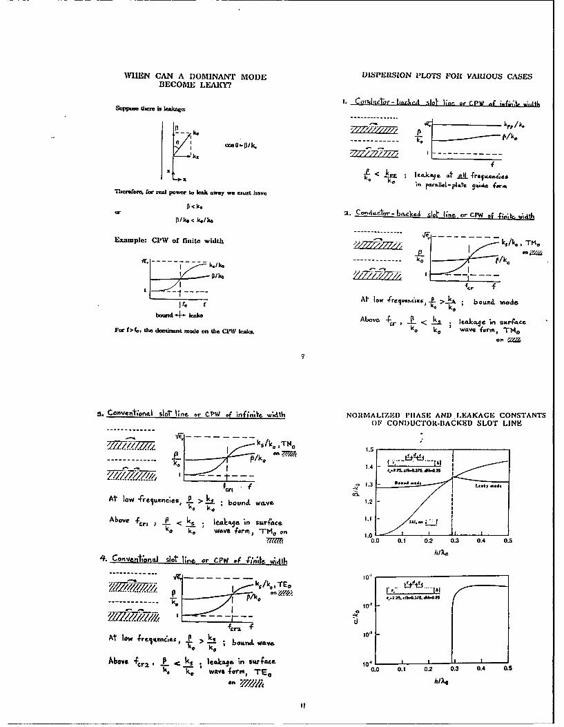
WIIEN CAN A DOMINANT MODE DISPERSION PLOTS FOR VAIUOUS CASESBECOME LEAI?.
I. Con'ci:tor- Ija kct. slo line of CPW 4 inn -iA. ;,j|1
Suppow wUre is l ckakc
k.k. os 0 l. ,--x--- ------/'i 7: k
k . Ie.kaje at all fretences
'n Fralle-plate Ji Ac -formTherefore, for rea power to leak away we must have
or D k. 2. Con4itcbr-bnLcked slat l ine or CFW of TIen;vo ;Jt,
pike < k./ko
Example: CPW of finite width k"/k0. TM,
---- ---- -----/- k, P
At low -rreijuenises -.% ~ bouncL mode
bound 4. lk A~ove <~ k, AL <Itakale 'in su.ace
For f>fc, the dominant mode on U CAlek k wave lerma'.o
on t
17
S. Convent,'oni.l slot line or CPW 4 infin; €e w;% NORMALIZE) PIIASE AND LEAKAGE CONSTANTSOF CONDUCTOt-BACKED SLOT LINE
'-T/ ksIk
° PTH° 1.5
on;
-- P -. /--- - n(., 1
At low -Freluenc;er, 1 >- ; 6 ounJ. wove 1.2
Above ;cr. I - _ eaIk&e in suwriace11TA.ko wave ;orm, 7Mo on 1.00 . 0.570.0 0.1I 0.2 0.3 0.4 0.
4. Conventona- slot line or CPw of ; Wfe 4,wad
------------- lO"i
p rI kl*T 0 *22. hOdS.~." /k, I T0"
-- -- - - -- -------------
Y110'
At low 4rcienice, > L, boi ml Wave.k, k,
Abov F1-2I k V vo o0 o. 0.2 0.3 0.4 0.5wav t;erm,& E0
NORMALIZED PHASE AND LEAKAGE CONSTANTSFOR MICROSTRIP LINE ON AN LEAKCAGE FROM hIIGHIER MODES ON
EPSILAM 10 SUBSTRATE 51ICROSTRIIP LINE4-0
TE, .1m.oe node
2.(jIo sna e av
30~~1. -regionloe~oeo
6 * 13.0 wlI*. 1.0
E1,. 10.3Cz. 13V 100
i.0 f i n GHz0 0.1 02 0.3 0IA 0.5
0.015 'I'icsolulions ame leaky where li~e curves ame showii,Ia~.I~ hi thsat trui.n ju.s alrnvc culagedT Um. SrffW Wnvc
Itnsrver a wide r.uigc or arigic. froin emiri.' to alnwst
Inxia(Wik a-, die fre. 1.ency ck'creaaes luermi cukdt
0.01 If (here is m., (ap cover, k-akagc alga owurs jnob slace
waves wIhers I/ ko 1.
0 0.1 02 03 0.1. 05h/A.
13
WAVEGUIDE DISCONTINUITIES
What occurs physically?
SOURCES OF CROSSTALK
Top viewro
1. Waveguido Discontinuities rnriesbnp
2. Lakage Effects
1. ll1icsL-Mlsm on the line are excited, butdecay away from it, and their power isessentially storml In the neighborhood of the
dliscontinuity. They provide reactance to the
equivalent netwvork of the discontinuity.
2. The lowesgt surface wave (or waves) en tEsurrounding substrate is excited, It riulint
power in surface - wave form ever a widerange of angles, and it provides resusance totlie equivalent network of the discontinuity.
3. If there are addigtional dominannt modir there
will ho some madle conversin Into them. This
effect contributes to resisance~
COWl a. NG -IEl'V.E-FN 'IAAlY Df)IS CO U ii,-.4G III,'Mw*,EN 'LEAK ' M~ODESANI)l'AICAC UUI)EI MO)I*AND P'ACKAGE GUIDED MODES
1. We ran view Use package guided niote in tcrim or apair of surfasen waves at an angle.
zf
lpView t cs0v'lo theJl ui oiuM Lnm~ rrweent the origina
(unperturbed), transmuision line assils andl pacluage guidedtodak espctively. lla solid linin reprentUwcope ail
2. 'Ilia akg ute uieasle x-l~llyfv Ivalqin' FURtTHJERIt NPOIUI ON
tilepacageguied 11(ilenogl ( '110 wo ndalesPacliage guilad made
We halil:
01" 1 H - At Co A
"Aeakfe mode
Bounnd snade
-- A-] A
:2/
EXCITATION OF PACKAGE G.UIDED) EXCITATION OF PACKCACE CAVITYMODES BY IJSCONTINUITIES RtESONANCES I1W DISCONTINUITIES
1. Ilia dicontinuity eciles suimlfmce waves at silt angle. sodust dUtLr j) valises ringe from 0 to I.
2. Mishlreliare, at a particular fl'aqmicncy. they cats coitlipe to nlpackager guided sateills it vitiaes in tiat range, astiedlya large umbuer a(thdem.
3. Inu die alassve cicamsple. 4 package guided mmotlies am ei'il.ihaca ~ ~ ca bwd~aaiinhlumuIlec via On, suwfa wave
4. lly cnitmiuad nn ieuiedms line iniale, wills a g~iven 11 at samppalad ItY ieintabele 11e eamplimig is ordinuarily fpd.r,'e~ney, f, emilli at "UW st mile (Coupile 140) :1 Anmgle Maill, li111 gvef lage at ft" I ,h Inmaua, a packaginepackage gi1de dc and ui pemlsaps none, isolmes ii -sity msiistU For a large packagte m siosantfrarquency iwiri eifeill lat-omee dm,4Y -,am In trequemney
Thecavty . aal hem~uudiemuame eeuplng orMsmak ca nb firwsel by Introucinlmg lam. but doe
rim~mauu at a rodse end as m a m aine a emumhInrrsna, in large pariwagme
23
CROSSTALK DUB TO LEAKAGE
CROSSTALK BETW11EEN LINES ANDDISCONTINUITIES Do the cuup c
YES
iscUEM'. at a djtLwilce!Is therecrosstallk?
2. T'wo Different Linecs
NO Do thy couple?
(The surface wave hiave witvenuiners; tUst. vary firoin k. to NO0 (ur ucgLuivc) ii, tie cuanipusaen along Usic line ksagtJ 'liary
will coupleonmly if dlic h. conimlmeacist is flI. Here, 0 > It.) Wi sand 1)i ummus be dieUse srnauc furcoupsling)
U:i. ir '['lie Is ai liscuatiaaufty oat the Sconad
//~i Is there Lisle,H s s aIl t C r o s s t a l k ?
P~ACKCAGE MODES wuxIr ihAPPENS TO LEAKAGEWHEN THlE P~ACKAGE! IS FINITE?
Two types: Guided rnodcsCavity modes
Infinite width Finite width
EXAMPLE OF GUIDED MODES
If inewa lioundlaig WALt' Cumnjliz wnvenumltier Real waversuulseir
'flu^. Uer. Is a simplle arelatioun between time package Muideil Iinusishirim last it in sol quomI dhoion at
uimes aral surfaces wave, an an unbousleit aulastrate. 'lire Us imt ant sill cn cause vtalk.
am manny package guidled macls faw eacls poild e rfave
way.. If A Is large, they amr clisely tiimsl in wnvencsnblxr.
3D MODELING OF MILLIMETER - WAVE CIRCUITS
AND ANTENNAS
N. Alexopoulos
UCLA • USA
00
o W 2U) .t L.>
4-o 04
o U
U) " "~Ut
aS, -4S~3 -
o.0 w-o C -4
sn 0 C)'
CI 4-> : : . ' )
o~C -b±'fb
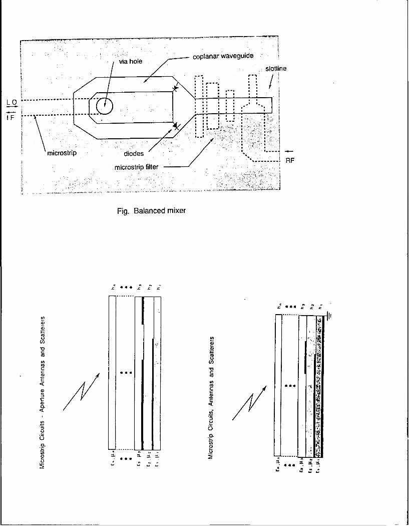
-43 ' U) I. 0
coplanar waveguide
microstrip diodes
microstrip filter R
Fig. Balanced mixer
2: 0*O , 77.,
0)0(n UC
C: 'D
4) <
(U;
-8 0.
Dipoles_
Fig. Lincar array of microstrip dipoles Fig Microstrip corporate feed
EnQ)0
040
~ ~ C4
o ~ ~ ( ni 0
bO 0
0- 0 CD~s.*0 CD -43
)d 43
;4 0 * -
00
0 0 U
100 20 Imilmil #2
0 .. . &GH& 8.8GHz 1 i
-10- 60
dB #3.20 -685-
* :1 950 mijl
a2 mil
1~ #4-40
0 30 40 90 120 13 g 160 mil0
Fig. 7. Allay ptaz
VSWR E#26
Fteq.acy (GHz) fo a8.5 GlHz
Fig.S. SWR skuh~quncyFig. 6. An embedded microstuip corporate feed
H-LA -
-W.80 mil
Od
Ld =442 mil, Od 1= iSl
- -- ';/IhI29miI
Fig. Electromignelically coupled] dipole red by a Inicrostripline ~ - Tile Magnaitude of fluicrostrip currenits in anl Isolated EMC dipole
co
00
CCV)
Lc)
4-
3 2
y U
"~ !
I: -- :xx., , '
Microstrip Linear Array of EMC Dipoles with a Corporate Feed
440 m&-A
I... * Relative current distribution in the output ports
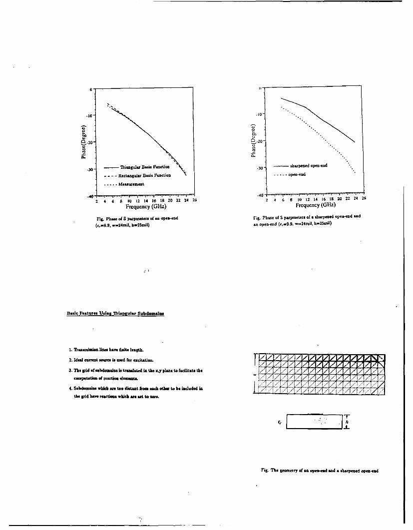
Fig. Phase of S parpmeters of an ope3end Fig. phase of S prpmeters of , sharpened open-end and
(c,-9.9, wI24mil, hI25mii) an open-end (c,=9i.9, w-fff24mil, h-25rmil)
Basic Features Using TJ[riangular Subdomalm
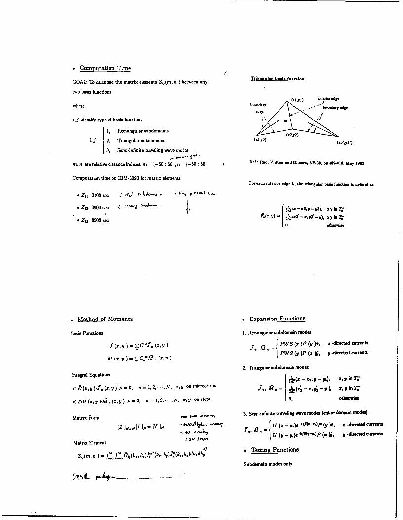
I. Tcanmission li ne have inuae lengt uo.
2.~~~ ~ IdaMurn or eas ufr exctan.t
3. Thea oid ofS abdomtos is optransdated in thePxs plane to facilitatethe"."..t... .. spnde .
c statio of reaction l, mi,- .... ..'..-.. -.. '.::.,:. . .' ;-_:_-.,_,....... -.:.""t"'"(4e too &6tam t from an opnen t.o. ..be.-.. .in l e i ...- .... ...h2..'l
the grid have reactins wich at o Ism
Fig- 71i gaometry Of n opetacad Iad t sharpened opee th
07 T TZT2z0.47
0.3 mitered bend
Right-angl bend .2
,04
03O miteed bend 0.1 Rgt-angle bend
02 . This theory- This theory -.
.01 .... ouviUle and jamnes' measuarement --- Douville and Jamee measurement
(t, = 1.0, b -300mirus. R = 1OO mils )(,= .L, b -30D mils. R - 1000Mills)e( * - , a =0.3063/rad, n E {O, 1, 2,3), 5 < p < 100 Mils (p - e*'al. 0.3063/red, n JO{0. 12.3), 5<P~.< 1000 ils)
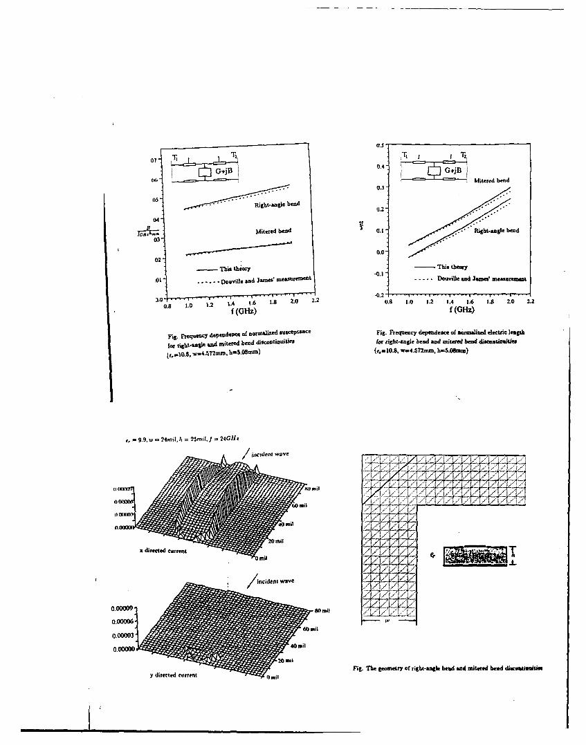
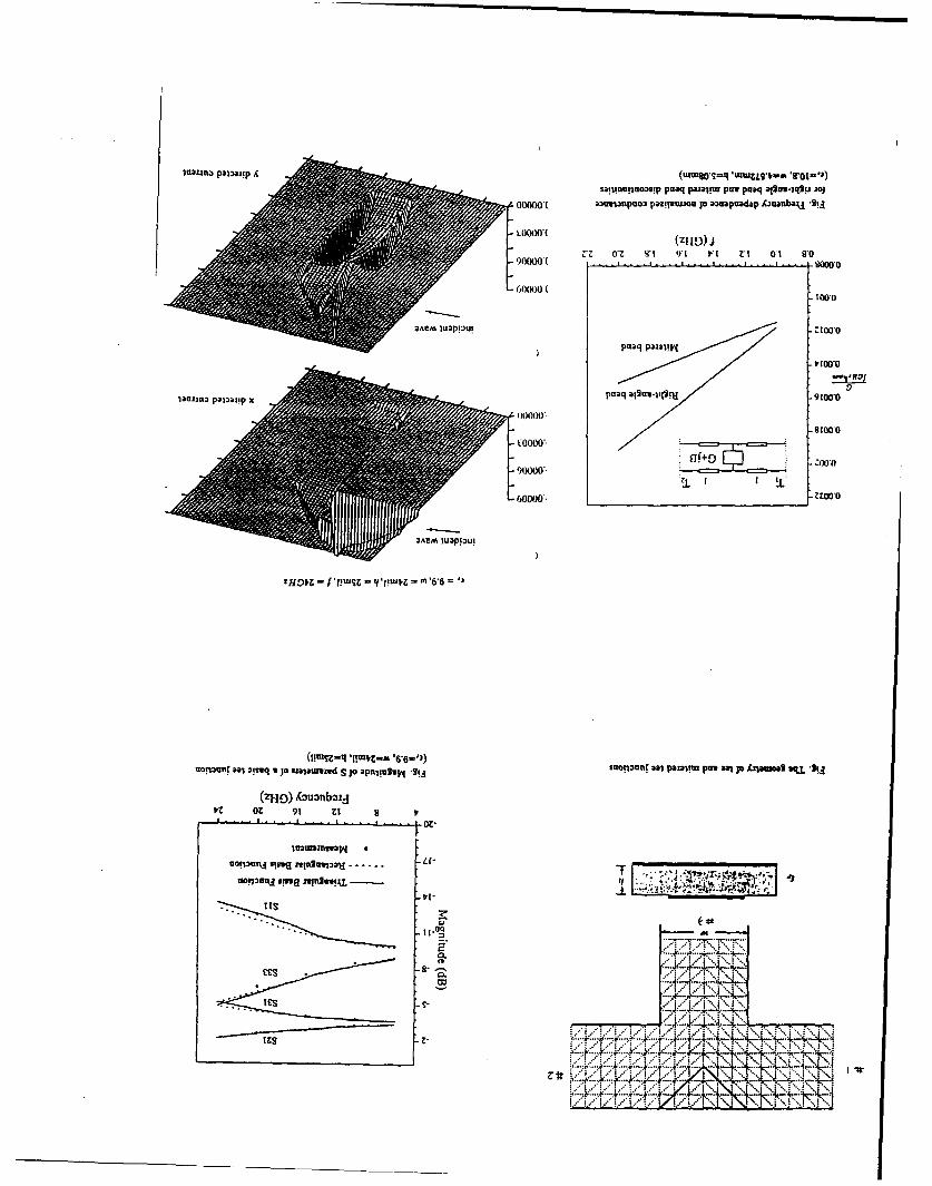
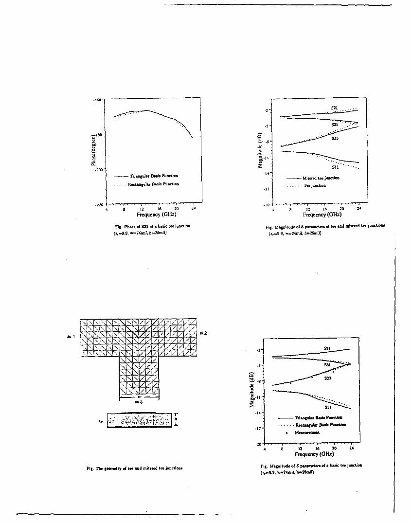
FREQUENCY DEPENDENT ANALYSIS OF PACKAGING PROBLEMSUSING TIlE THREE-DIMENSIONAL INTEGRAL EQUATIONS TECHNIQUE
II. GIIALI*, M. DRISSI*, J. CITERNE* and V. FOUAD IIANNA**
*Laboratoirc Composants et Syst6mcs pour T6l6communications
URA 834, INSA, 35043 RENNES, FRANCE**CNET/PAB, 92131 ISSY LES MOULINEAUX, FRANCE
ABSTRACTThe main problems associated with packaging technique for microwavc and millimeterintegrated or monolithic circuits are the shielding effects, discontinuity and chip connectionscharacterization. In this paper, a dynamic analysis, based on the three-dimensional integralequations technique associated with the method of moments is presented for thecharacterization of shicldcd discontinuity problems. It uses the three-dimensional Green'sfunction for a general current distribution inside a shielded box. The theory of loadcdscatterers is also used to take into account the effect of existing localized and distributedactive devices or passive loads. Using this last theory, a virtual matched load is simulated,numerically, by introducing localized absorbing loads at circuit sections c3rresponding tooutput ports. Consequently, a scattering parameters extraction technique, based on the use ofthese matched terminations, is developed, and hence the [S] parameters of the studieddiscontinuity are determined from the knowledge of only current or electric field maximawhich are often accurately determined under good matching conditions. The shielding effectson a wide range of planar and three-dimensional discontinuities are given. The behaviour of atypical chip connection as a strip air bridge is also studied and the frequency dependentcharacteristics of these discontinuities are presented.
00
g's 8 2 F7 0 .5
'0 .0 N
,a =0 .n .0
aX -u ;s -E-
-I--
@1 0 0
S. -~.: - t=Is~ E.ut5 5; a=
0 0 ~ o 0 ell
u,24's -- - . c
- =-c 0 a; o)
L5-- .o' -- o
9z '20 u 0E or~ -oc
Cd, o u 0 - c t3 o ot IP. , 0 0'4 o -
5 >: 20. 0v705 o ' u. u-- 3. .. a
2000
00 *5= 00 it
0 r cu u -y
0 0c~~n 0 r-t =t.2 .0 '.0fU'cCf4j
0Z L. ,uc
o r,. r mu-2 o 00 C,. t. a 1:or
rn ' 5- ou- ;o- qua L3 - c60 00
*~~~ ~~~~ M-0 OOll ~~O * u J U2 <
3/)~~~~ Oun 4 o O'',u.
-:U uu - 5 0"'0
as E - - -50 S
.~ ........
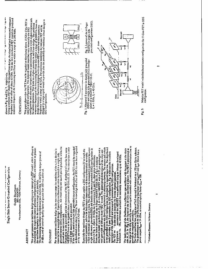
Fig. 4: Measured and m~odeled S-Paramecer Fig. 5: Layout of the Oscillator.in snlsiegrounded configuration(SSG).
36.25 UA
36.1
-I .1.5 -0.9 -0.05 .0.6 0 ,47S .0? *Or. .0.6
U" M
Fig. 6: Rcsonancc frequency vs gate- and drain voltage.
'3
P0 15 (dDlo) 12~4
10
.1I -0.95 -0,9 4AS5 4.8 -. 7S .0.7 .0.65 40.6
Fig. 7: Output power vs gat(-- and drain voltage.
Refereces:
I/ W. Hecinrich, "Limits or F1TT Modclting by Lumped Elemnents". E lecironacs Letters, vol. 22. no. 12, S.630-632. Juni 1986
/21 H.P. Fcldlc, "Klein- und Grolgsignal.CAD-Modclic von GaAs MESFETs mit vcrlicnt Elcmentcn",Dissertation Univcrsitat Karlsrulic, 1987
/31 G. Baumann. R. Hierl. "Modular FET model with distributed source configuration for a single anddouble side source grounded MESFEr. Ekcctronics~Uacrs, vol. 27, no. 13, S. 1128-1129, Juni 1991
/4/ K. Kutokawa. *Some Basic Charactcristics or Broadband Negative Resistance Oscillator Circuits%,Pie Bell SystcrnuTechnical Journal, Juli- August. 1969
151 George 1). Vcndclin. Design of Amplifiers and Oscillators by (lhe S-Paramctcr Method. John Wilceyand Sons, Inc.. 1982