Quad-Channel Isolators with Integrated DC-to-DC Converters
Data Sheet ADuM5410/ADuM5411/ADuM5412
Rev. 0 Document Feedback Information furnished by Analog Devices is believed to be accurate and reliable. However, no responsibility is assumed by Analog Devices for its use, nor for any infringements of patents or other rights of third parties that may result from its use. Specifications subject to change without notice. No license is granted by implication or otherwise under any patent or patent rights of Analog Devices. Trademarks and registered trademarks are the property of their respective owners.
FEATURES isoPower integrated, isolated dc-to-dc converter Up to 150 mW output power Quad dc to 150 Mbps signal isolation channels 24-lead SSOP package with 5.3 mm minimum creepage High temperature operation: 105°C High common-mode transient immunity: 100 kV/μs Safety and regulatory approvals
UL recognition (pending) 2500 V rms for 1 minute per UL 1577
DIN V VDE V 0884-10 (VDE V 0884-10):2006-12 VIORM = 565 V peak
APPLICATIONS RS-232 transceivers Power supply startup bias and gate drives Isolated sensor interfaces Industrial PLCs
GENERAL DESCRIPTION The ADuM5410/ADuM5411/ADuM54121 are quad-channel digital isolators with isoPower®, integrated, isolated dc-to-dc converters. Based on the Analog Devices, Inc., iCoupler® technology, the dc-to-dc converters provide regulated, isolated power that is adjustable between 3.15 V and 5.25 V. Popular voltage combinations and the associated power levels are shown in Table 1.
The ADuM5410/ADuM5411/ADuM5412 eliminate the need for a separate, isolated dc-to-dc converter in low power, isolated designs. The iCoupler chip scale transformer technology is used for isolated logic signals and for the magnetic components of the dc-to-dc converters. The result is a small form factor, total isolation solution.
The ADuM5410/ADuM5411/ADuM5412 isolators provide four independent isolation channels in a variety of channel configura-tions and data rates (see the Ordering Guide for more information).
FUNCTIONAL BLOCK DIAGRAM
GND1
I/O1B
I/O1A
VDD1
I/O1C
I/O2B
I/O2A
I/O2C
I/O1D
VE1
NIC
VDDP
GND1
GND1
PDIS
VDD2
GNDISO
I/O2D
VSEL
GNDISO
VISO
VE2
NIC
GNDISO
1
2
3
4
5
6
7
8
9
10
11
12
14
13
20
19
18
17
16
23
24
22
21
15
OSC RECT REG
PCS
NIC = NO INTERNAL CONNECTION. LEAVE THIS PIN FLOATING.
4-CHANNEL iCoupler CORE
ADuM5410/ADuM5411/ADuM5412
1469
5-00
1
Figure 1.
Table 1. Power Levels Input Voltage (V) Output Voltage (V) Output Power (mW) 5 5 150 5 3.3 100 3.3 3.3 66
Table 2. Data Input/Output Port Assignments Ch. Pin No. ADuM5410 ADuM5411 ADuM5412 I/O1A 3 VIA VIA VIA I/O1B 4 VIB VIB VIB
I/O1C 5 VIC VIC VOC I/O1D 6 VID VOD VOD
I/O2A 22 VOA VOA VOA I/O2B 21 VOB VOB VOB
I/O2C 20 VOC VOC VIC I/O2D 19 VOD VID VID
1 Protected by U.S. Patents 5,952,849; 6,873,065; 6,903,578; and 7,075,329. Other patents are pending.
TABLE OF CONTENTS Features .............................................................................................. 1 Applications ....................................................................................... 1 General Description ......................................................................... 1 Functional Block Digram ................................................................ 1 Revision History ............................................................................... 2 Specifications ..................................................................................... 3
Electrical Characteristics—5 V Primary Input Supply/5 V Secondary Isolated Supply........................................................... 3 Electrical Characteristics—3.3 V Primary Input Supply/3.3 V Secondary Isolated Supply........................................................... 5 Electrical Characteristics—5 V Primary Input Supply/3.3 V Secondary Isolated Supply........................................................... 7 Electrical Characteristics—2.5 V Operation Digital Isolator Channels Only .............................................................................. 9 Electrical Characteristics—1.8 V Operation Digital Isolator Channels Only ............................................................................ 11 Package Characteristics ............................................................. 13 Regulatory Approvals ................................................................. 13 Insulation and Safety Related Specifications .......................... 13
DIN V VDE V 0884-10 (VDE V 0884-10) Insulation Characteristics ............................................................................ 14 Recommended Operating Conditions .................................... 14
Absolute Maximum Ratings ......................................................... 15 ESD Caution................................................................................ 15
Pin Configurations and Function Descriptions ......................... 16 Truth Tables................................................................................. 19
Typical Performance Characteristics ........................................... 20 Terminology .................................................................................... 24 Theory of Operation ...................................................................... 25 Applications Information .............................................................. 26
REVISION HISTORY 7/2016—Revision 0: Initial Version
Data Sheet ADuM5410/ADuM5411/ADuM5412
Rev. 0 | Page 3 of 29
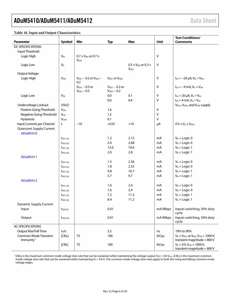
SPECIFICATIONS ELECTRICAL CHARACTERISTICS—5 V PRIMARY INPUT SUPPLY/5 V SECONDARY ISOLATED SUPPLY All typical specifications are at TA = 25°C, VDD1 = VDDP = VISO = 5 V, VSEL resistor network: R1 = 10 kΩ ±1%, R2 = 30.9 kΩ ± 1% between VISO and GNDISO (see Figure 31). Minimum/maximum specifications apply over the entire recommended operation range, which is 4.5 V ≤ VDD1, VDDP, VISO ≤ 5.5 V, and −40°C ≤ TA ≤ +105°C, unless otherwise noted. Switching specifications are tested with CL = 15 pF and CMOS signal levels, unless otherwise noted.
Table 3. DC-to-DC Converters Static Specifications Parameter Symbol Min Typ Max Unit Test Conditions/Comments DC-TO-DC CONVERTERS SUPPLY
Setpoint VISO 4.7 5.0 5.4 V IISO = 15 mA, R1 = 10 kΩ, R2 = 30.9 kΩ Line Regulation VISO (LINE) 20 mV/V IISO = 15 mA, VDDP = 4.5 V to 5.5 V Load Regulation VISO (LOAD) 1 5 % IISO = 3 mA to 27 mA Output Ripple VISO (RIP) 75 mV p-p 20 MHz bandwidth, CBO = 0.1 µF||10 µF, IISO = 27 mA Output Noise VISO (NOISE) 200 mV p-p CBO = 0.1 µF||10 µF, IISO = 27 mA Switching Frequency fOSC 125 MHz Pulse-Width Modulation Frequency fPWM 600 kHz Output Supply IISO (MAX) 30 mA VISO > 4.5 V Efficiency at IISO (MAX) 29 % IISO = 27 mA VDDP Supply Current
No VISO Load IDDP (Q) 14 20 mA Full VISO Load IDDP (MAX) 104 140 mA
Thermal Shutdown Shutdown Temperature 154 °C Thermal Hysteresis 10 °C
Table 4. Data Channel Supply Current Specifications 1 Mbps 25 Mbps 100 Mbps Parameter Symbol Min Typ Max Min Typ Max Min Typ Max Unit Test Conditions/Comments SUPPLY CURRENT CL = 0 pF
ADuM5410 IDD1 6.8 10 7.8 12 11.8 17.4 mA IDD2 2.1 3.7 3.9 5.7 9.2 13 mA ADuM5411 IDD1 5.8 10.3 7.0 10.9 11.4 15.9 mA IDD2 4.0 6.85 5.5 8.5 10.3 14.0 mA ADuM5412 IDD1 4.3 7.7 6.0 9.3 10.3 14.2 mA IDD2 5.3 8.7 6.7 10.1 11.0 14.9 mA
Table 5. Switching Specifications Parameter Symbol Min Typ Max Unit Test Conditions/Comments SWITCHING SPECIFICATIONS
Pulse Width PW 6.6 ns Within pulse width distortion (PWD) limit Data Rate 150 Mbps Within PWD limit Propagation Delay tPHL, tPLH 4.8 7.2 13 ns 50% input to 50% output Pulse Width Distortion PWD 0.5 3 ns |tPLH − tPHL| Change vs. Temperature 1.5 ps/°C Propagation Delay Skew tPSK 6.1 ns Between any two units at the same temperature, voltage, and load Channel Matching
1 IOx is the Channel x output current, where x means A, B, C, or D. 2 VIxH is the input side logic high. 3 VIxL is the input side logic low. 4 |CMH| is the maximum common-mode voltage slew rate that can be sustained while maintaining the voltage output (VO) > 0.8 VDDx. |CML| is the maximum common-
mode voltage slew rate that can be sustained while maintaining VO > 0.8 V. The common-mode voltage slew rates apply to both the rising and falling common-mode voltage edges.
ELECTRICAL CHARACTERISTICS—3.3 V PRIMARY INPUT SUPPLY/3.3 V SECONDARY ISOLATED SUPPLY All typical specifications are at TA = 25°C, VDD1 = VDDP = VISO = 3.3 V, VSEL resistor network: R1 = 10 kΩ, ±1%, R2 = 16.9 kΩ ± 1% between VISO and GNDISO (see Figure 31). Minimum/maximum specifications apply over the entire recommended operation range, which is 3.0 V ≤ VDD1, VDDP, VISO ≤ 3.6 V, and −40°C ≤ TA ≤ +105°C, unless otherwise noted. Switching specifications are tested with CL = 15 pF and CMOS signal levels, unless otherwise noted.
Table 7. DC-to-DC Converter Static Specifications Parameter Symbol Min Typ Max Unit Test Conditions/Comments DC-TO-DC CONVERTER SUPPLY
Setpoint VISO 3.0 3.3 3.6 V IISO = 10 mA, R1 = 10 kΩ, R2 = 16.9 kΩ Line Regulation VISO (LINE) 20 mV/V IISO = 10 mA, VDD1 = 3.0 V to 3.6 V Load Regulation VISO (LOAD) 1 5 % IISO = 2 mA to 18 mA Output Ripple VISO (RIP) 50 mV p-p 20 MHz bandwidth, CBO = 0.1 µF||10 µF, IISO = 18 mA Output Noise VISO (NOISE) 130 mV p-p CBO = 0.1 µF||10 µF, IISO = 18 mA Switching Frequency fOSC 125 MHz Pulse-Width Modulation Frequency fPWM 600 kHz Output Supply IISO (MAX) 20 mA 3.6 V > VISO > 3 V Efficiency at IISO (MAX) 27 % IISO = 18 mA VDDP Supply Current
No VISO Load IDDP (Q) 14 20 mA Full VISO Load IDDP (MAX) 77 115 mA
Thermal Shutdown Shutdown Temperature 154 °C Thermal Hysteresis 10 °C
Table 8. Data Channel Supply Current Specifications 1 Mbps 25 Mbps 100 Mbps Parameter Symbol Min Typ Max Min Typ Max Min Typ Max Unit Test Conditions/Comments SUPPLY CURRENT CL = 0 pF
ADuM5410 IDD1 6.6 9.8 7.4 11.2 10.7 15.9 mA IDD2 2.0 3.7 3.5 5.5 8.2 11.6 mA ADuM5411 IDD1 5.65 10.1 6.65 10.5 10.4 14.9 mA IDD2 3.9 6.65 5.2 8.0 9.4 12.8 mA ADuM5412 IDD1 4.3 7.7 5.6 9.0 9.1 13 mA IDD2 5.0 8.4 6.2 9.6 9.8 13.7 mA
Table 9. Switching Specifications Parameter Symbol Min Typ Max Unit Test Conditions/Comments SWITCHING SPECIFICATIONS
Pulse Width PW 6.7 ns Within PWD limit Data Rate 150 Mbps Within PWD limit Propagation Delay tPHL, tPLH 6.8 14 ns 50% input to 50% output Pulse Width Distortion PWD 0.7 3.0 ns |tPLH − tPHL| Change vs. Temperature 1.5 ps/°C Propagation Delay Skew tPSK 7.5 ns Between any two units at the same temperature, voltage, and load Channel Matching
transient magnitude = 800 V 1 |CMH| is the maximum common-mode voltage slew rate that can be sustained while maintaining the voltage output (VO) > 0.8 VDDx. |CML| is the maximum common-
mode voltage slew rate that can be sustained while maintaining VO > 0.8 V. The common-mode voltage slew rates apply to both the rising and falling common-mode voltage edges.
ELECTRICAL CHARACTERISTICS—5 V PRIMARY INPUT SUPPLY/3.3 V SECONDARY ISOLATED SUPPLY All typical specifications are at TA = 25°C, VDD1 = VDDP = 5.0 V, VISO = 3.3 V, VSEL resistor network: R1 = 10 kΩ ± 1%, R2 = 16.9 kΩ ±1% between VISO and GNDISO (see Figure 31). Minimum/maximum specifications apply over the entire recommended operation range, which is 4.5 V ≤ VDD1 = VDDP ≤ 5.5 V, 3.0 V ≤ VISO ≤ 3.6 V, and −40°C ≤ TA ≤ +105°C, unless otherwise noted. Switching specifications are tested with CL = 15 pF and CMOS signal levels, unless otherwise noted.
Table 11. DC-to-DC Converter Static Specifications Parameter Symbol Min Typ Max Unit Test Conditions/Comments DC-TO-DC CONVERTER SUPPLY
Setpoint VISO 3.0 3.3 3.6 V IISO = 15 mA, R1 = 10 kΩ, R2 = 16.9 kΩ Line Regulation VISO (LINE) 20 mV/V IISO = 15 mA, VDD1 = 3.0 V to 3.6 V Load Regulation VISO (LOAD) 1 5 % IISO = 3 mA to 27 mA Output Ripple VISO (RIP) 50 mV p-p 20 MHz bandwidth, CBO = 0.1 µF||10 µF, IISO = 27 mA Output Noise VISO (NOISE) 130 mV p-p CBO = 0.1 µF||10 µF, IISO = 27 mA Switching Frequency fOSC 125 MHz Pulse-Width Modulation Frequency fPWM 600 kHz Output Supply IISO (MAX) 30 mA 3.6 V > VISO > 3 V Efficiency at IISO (MAX) 24 % IISO = 27 mA VDDP Supply Current
No VISO Load IDDP (Q) 14 20 mA Full VISO Load IDDP (MAX) 85 115 mA
Thermal Shutdown Shutdown Temperature 154 °C Thermal Hysteresis 10 °C
Table 12. Data Channel Supply Current Specifications 1 Mbps 25 Mbps 100 Mbps Parameter Symbol Min Typ Max Min Typ Max Min Typ Max Unit Test Conditions/Comments SUPPLY CURRENT CL = 0 pF
ADuM5410 IDD1 6.8 10 7.8 12 11.8 17.4 mA IDD2 2.0 3.7 3.5 5.5 8.2 11.6 mA ADuM5411 IDD1 5.8 10.3 7.0 10.9 11.4 15.9 mA IDD2 3.9 6.65 5.2 8.0 9.4 12.8 mA ADuM5412 IDD1 4.3 7.7 6.0 9.3 10.3 14.2 mA IDD2 5.0 8.4 6.2 9.6 9.8 13.7 mA
Table 13. Switching Specifications Parameter Symbol Min Typ Max Unit Test Conditions/Comments SWITCHING SPECIFICATIONS
Pulse Width PW 6.7 ns Within PWD limit Data Rate 150 Mbps Within PWD limit Propagation Delay tPHL, tPLH 6.8 14 ns 50% input to 50% output Pulse Width Distortion PWD 0.7 3.0 ns |tPLH − tPHL| Change vs. Temperature 1.5 ps/°C Propagation Delay Skew tPSK 7.5 ns Between any two units at the same temperature, voltage, and load Channel Matching
transient magnitude = 800 V 1 |CMH| is the maximum common-mode voltage slew rate that can be sustained while maintaining the voltage output (VO) > 0.8 VDDx. |CML| is the maximum common-
mode voltage slew rate that can be sustained while maintaining VO > 0.8 V. The common-mode voltage slew rates apply to both the rising and falling common-mode voltage edges.
ELECTRICAL CHARACTERISTICS—2.5 V OPERATION DIGITAL ISOLATOR CHANNELS ONLY All typical specifications are at TA = 25°C, VDD1 = VDD2 = 2.5 V. Minimum/maximum specifications apply over the entire recommended operation range: 2.25 V ≤ VDD1 ≤ 2.75 V, 2.25 V ≤ VDD2 ≤ 2.75 V, −40°C ≤ TA ≤ +105°C, unless otherwise noted. Switching specifications are tested with CL = 15 pF and CMOS signal levels, unless otherwise noted. Supply currents are specified with 50% duty cycle signals.
Table 15. Data Channel Supply Current Specifications 1 Mbps 25 Mbps 100 Mbps Parameter Symbol Min Typ Max Min Typ Max Min Typ Max Unit Test Conditions/Comments SUPPLY CURRENT CL = 0 pF
ADuM5410 IDD1 6.5 9.8 7.3 11.1 10.4 15.5 mA IDD2 2.0 3.6 3.3 5.2 7.3 10.2 mA ADuM5411 IDD1 5.6 10.0 6.4 10.4 9.7 14.5 mA IDD2 3.8 6.55 4.8 7.7 8.3 11.5 mA ADuM5412 IDD1 4.3 7.7 5.4 8.8 8.8 12.7 mA IDD2 5.0 8.4 6.1 9.5 9.5 13.4 mA
Table 16. Switching Specifications Parameter Symbol Min Typ Max Unit Test Conditions/Comments SWITCHING SPECIFICATIONS
Pulse Width PW 6.6 ns Within PWD limit Data Rate 150 Mbps Within PWD limit Propagation Delay tPHL, tPLH 5.0 7.0 14 ns 50% input to 50% output Pulse Width Distortion PWD 0.7 3 ns |tPLH − tPHL| Change vs. Temperature 1.5 ps/°C Propagation Delay Skew tPSK 6.8 ns Between any two units at the same temperature, voltage, and
transient magnitude = 800 V 1 |CMH| is the maximum common-mode voltage slew rate that can be sustained while maintaining the voltage output (VO) > 0.8 VDDx. |CML| is the maximum common-
mode voltage slew rate that can be sustained while maintaining VO > 0.8 V. The common-mode voltage slew rates apply to both the rising and falling common-mode voltage edges.
ELECTRICAL CHARACTERISTICS—1.8 V OPERATION DIGITAL ISOLATOR CHANNELS ONLY All typical specifications are at TA = 25°C, VDD1 = VDD2 = 1.8 V. Minimum/maximum specifications apply over the entire recommended operation range: 1.7 V ≤ VDD1 ≤ 1.9 V, 1.7 V ≤ VDD2 ≤ 1.9 V, and −40°C ≤ TA ≤ +105°C, unless otherwise noted. Switching specifications are tested with CL = 15 pF and CMOS signal levels, unless otherwise noted. Supply currents are specified with 50% duty cycle signals.
Table 18. Data Channel Supply Current Specifications 1 Mbps 25 Mbps 100 Mbps Parameter Symbol Min Typ Max Min Typ Max Min Typ Max Unit Test Conditions/Comments SUPPLY CURRENT CL = 0 pF
ADuM5410 IDD1 6.4 9.8 7.2 11 10.2 15.2 mA IDD2 1.9 3.5 3.1 5.0 6.8 10 mA ADuM5411 IDD1 5.5 9.1 6.3 10.0 9.6 14.0 mA IDD2 3.72 6.45 4.8 7.5 8.4 11.2 mA ADuM5412 IDD1 4.3 7.7 5.3 8.7 8.6 12.6 mA IDD2 4.9 8.3 6.0 9.4 9.3 13.3 mA
Table 19. Switching Specifications Parameter Symbol Min Typ Max Unit Test Conditions/Comments SWITCHING SPECIFICATIONS
Pulse Width PW 6.6 ns Within PWD limit Data Rate 150 Mbps Within PWD limit Propagation Delay tPHL, tPLH 5.8 8.7 15 ns 50% input to 50% output Pulse Width Distortion PWD 0.7 3 ns |tPLH − tPHL| Change vs. Temperature 1.5 ps/°C Propagation Delay Skew tPSK 7.0 ns Between any two units at the same temperature, voltage, and
transient magnitude = 800 V 1 |CMH| is the maximum common-mode voltage slew rate that can be sustained while maintaining the voltage output (VO) > 0.8 VDDx. |CML| is the maximum common-
mode voltage slew rate that can be sustained while maintaining VO > 0.8 V. The common-mode voltage slew rates apply to both the rising and falling common-mode voltage edges.
Table 21. Thermal and Isolation Characteristics Parameter Symbol Min Typ Max Unit Test Conditions/Comments Resistance (Input to Output)1 RI-O 1012 Ω Capacitance (Input to Output)1 CI-O 2.2 pF f = 1 MHz Input Capacitance2 CI 4.0 pF IC Junction to Ambient Thermal Resistance θJA 50 °C/W Thermocouple located at center of package underside,
test conducted on 4-layer board with thin traces3 1 The device is considered a 2-terminal device: Pin 1 to Pin 8 are shorted together, and Pin 9 to Pin 16 are shorted together. 2 Input capacitance is from any input data pin to ground. 3 See the Thermal Analysis section for thermal model definitions.
CSA 60950-1-07+A1+A2 and IEC 60950-1, second edition, +A1+A2:
Reinforced Insulation 565 V peak, VIOSM = 4 kV peak
GB4943.1-2011:
Basic insulation at 400 V rms (565 V peak)
Basic insulation (1MOPP), 250 V rms (354 V peak)
Basic insulation at 400 V rms (565 V peak)
CSA 61010-1-12 and IEC 61010-1 third edition
Basic insulation at 300 V rms mains, 530 V rms (750 V peak)
File E214100 File 205078 File 2471900-4880-0001 File (pending) 1 In accordance with UL 1577, each ADuM5410/ADuM5411/ADuM5412 is proof tested by applying an insulation test voltage ≥ 3000 V rms for 1 second (current leakage
detection limit = 10 µA). 2 In accordance with DIN V VDE V 0884-10, each ADuM5410/ADuM5411/ADuM5412 is proof tested by applying an insulation test voltage ≥1050 V peak for 1 second
(partial discharge detection limit = 5 pC). The * marking branded on the component designates DIN V VDE V 0884-10 approval.
INSULATION AND SAFETY RELATED SPECIFICATIONS
Table 23. Critical Safety Related Dimensions and Material Properties Parameter Symbol Value Unit Test Conditions/Comments Rated Dielectric Insulation Voltage 2500 V rms 1-minute duration Minimum External Air Gap (Clearance) L(I01) 5.3 mm min Measured from input terminals to output terminals,
shortest distance through air Minimum External Tracking (Creepage) L(I02) 5.3 mm min Measured from input terminals to output terminals,
shortest distance path along body Minimum Clearance in the Plane of the Printed
Circuit Board (PCB Clearance) L (PCB) 5.6 mm min Measured from input terminals to output terminals,
shortest distance through air, line of sight, in the PCB mounting plane
Minimum Internal Gap (Internal Clearance) 17 μm min Minimum distance through insulation Tracking Resistance (Comparative Tracking Index) CTI >400 V DIN IEC 112/VDE 0303, Part 1 Isolation Group II Material group (DIN VDE 0110, 1/89, Table 1)
DIN V VDE V 0884-10 (VDE V 0884-10) INSULATION CHARACTERISTICS These isolators are suitable for reinforced electrical isolation only within the safety limit data. Maintenance of the safety data is ensured by the protective circuits. The asterisk (*) marking on packages denotes DIN V VDE V 0884-10 approval.
Table 24. VDE Characteristics Description Test Conditions/Comments Symbol Characteristic Unit Installation Classification per DIN VDE 0110
For Rated Mains Voltage ≤ 150 V rms I to IV For Rated Mains Voltage ≤ 300 V rms I to IV For Rated Mains Voltage ≤ 400 V rms I to III
Climatic Classification 40/105/21 Pollution Degree per DIN VDE 0110, Table 1 2 Maximum Working Insulation Voltage VIORM 565 V peak Input to Output Test Voltage, Method b1 VIORM × 1.875 = VPR, 100% production test, tm = 1 sec,
partial discharge < 5 pC VPR 1059 V peak
Input to Output Test Voltage, Method a VPR After Environmental Tests Subgroup 1 VIORM × 1.5 = Vpd(m), tini = 60 sec, tm = 10 sec,
partial discharge < 5 pC Vpd(m) 848 V peak
After Input and/or Safety Test Subgroup 2 and Subgroup 3
VIORM × 1.2 = Vpd(m), tini = 60 sec, tm = 10 sec, partial discharge < 5 pC
Vpd(m) 678 V peak
Highest Allowable Overvoltage Transient overvoltage, tTR = 10 sec VIOTM 3535 V peak Withstand Isolation Voltage 1 minute withstand rating VISO 2500 V rms Surge Isolation Voltage Basic VIOSM(TEST) = 10 kV; 1.2 µs rise time; 50 µs, 50% fall time VISOM 4000 V peak Safety Limiting Values Maximum value allowed in the event of a failure
(see Figure 2)
Case Temperature TS 150 °C Total Power Dissipation at 25°C IS1 2.5 W
Insulation Resistance at TS VIO = 500 V RS >109 Ω
0
0.5
1.0
1.5
2.0
2.5
3.0
0 50 100 150 200
SAFE
LIM
ITIN
G P
OW
ER (W
)
1469
5-00
2
Figure 2. Thermal Derating Curve, Dependence of Safety Limiting Values on
Case Temperature, per DIN EN 60747-5-2
RECOMMENDED OPERATING CONDITIONS
Table 25. Parameter Symbol Min Max Unit Operating Temperature1 TA −40 +105 °C Supply Voltages2
VDDP at VISO = 3.0 V to 3.6 V VDDP 3.0 5.5 V VDDP at VISO = 4.5 V to 5.5 V 4.5 5.5 V VDD1, VDD2 VDD1, VDD2 1.7 5.5 V
1 Operation at 105°C requires reduction of the maximum load current as
specified in Table 26. 2 Each voltage is relative to its respective ground.
Data Sheet ADuM5410/ADuM5411/ADuM5412
Rev. 0 | Page 15 of 29
ABSOLUTE MAXIMUM RATINGS Ambient temperature (TA) = 25°C, unless otherwise noted.
Table 26. Parameter Rating Storage Temperature (TST) −55°C to +150°C Ambient Operating Temperature (TA) −40°C to +105°C Supply Voltages (VDD1, VDDP, VDD2, VISO)1 −0.5 V to +7.0 V VISO Supply Current2
TA = −40°C to +105°C 30 mA Input Voltage (VIA, VIB, VIC, VID,VE1, VE2,
VSEL, PDIS)1, 3 −0.5 V to VDDI + 0.5 V
Output Voltage (VOA, VOB, VOC, VOD)1, 3 −0.5 V to VDDO + 0.5 V Average Output Current Per Data
Output Pin4 −10 mA to +10 mA
Common-Mode Transients5 −150 kV/µs to +150 kV/µs 1 All voltages are relative to their respective ground. 2 The VISO pin provides current for dc and dynamic loads on the VISO
input/output channels. This current must be included when determining the total VISO supply current. For ambient temperatures between 85°C and 105°C, the maximum allowed current is reduced.
3 VDDI and VDDO refer to the supply voltages on the input and output sides of a given channel, respectively. See the PCB Layout section.
4 See Figure 2 for the maximum rated current values for various temperatures. 5 Common-mode transients refers to common-mode transients across the
insulation barrier. Common-mode transients exceeding the absolute maximum ratings may cause latch-up or permanent damage.
Stresses at or above those listed under Absolute Maximum Ratings may cause permanent damage to the product. This is a stress rating only; functional operation of the product at these or any other conditions above those indicated in the operational section of this specification is not implied. Operation beyond the maximum operating conditions for extended periods may affect product reliability.
Table 27. Maximum Continuous Working Voltage Supporting 50-Year Minimum Lifetime1
Parameter Max Unit Applicable Certification
AC Voltage Bipolar Waveform 560 V peak All certifications,
50-year operation
Unipolar Waveform Basic Insulation 560 V peak
DC Voltage Basic Insulation 560 V peak
1 Maximum continuous working voltage refers to the continuous voltage magnitude imposed across the isolation barrier. See the Insulation Lifetime section for more information.
ESD CAUTION
ADuM5410/ADuM5411/ADuM5412 Data Sheet
Rev. 0 | Page 16 of 29
PIN CONFIGURATIONS AND FUNCTION DESCRIPTIONS
1
2
3
4
24
23
22
21
5 20
6 19
7 18
8
9
10
17
16
15
11
12
14
13
ADuM5410TOP VIEW
(Not to Scale)
NIC = NO INTERNAL CONNECTION.LEAVE THESE PINS FLOATING.
GND1
VIB
VIA
VDD1
VIC
VOB
VOA
VOC
VID
NIC
NIC
VDDP
GND1
GND1
PDIS
VDD2
GNDISO
VOD
VSEL
GNDISO
VISO
VE2
NIC
GNDISO
1469
5-00
3
Figure 3. ADuM5410 Pin Configuration
Table 28. ADuM5410 Pin Function Descriptions Pin No. Mnemonic Description 1 VDD1 Power Supply for the Side 1 Logic Circuits of the Device. This pin is independent of VDDP and operates between 3.0 V
and 5.5 V. 2, 9, 12 GND1 Ground 1. Ground reference for the primary isolator. Pin 2, Pin 9, and Pin 12 are internally connected, and it is
recommended that these pins be connected to a common ground. 3 VIA Logic Input A. 4 VIB Logic Input B. 5 VIC Logic Input C. 6 VID Logic Input D. 7, 8, 17 NIC No Internal Connection. Leave these pins floating. 10 PDIS Power Disable. When tied to any GND1 pin, the power converter is active; when a logic high voltage is applied, the
power supply enters a low power standby mode. 11 VDDP Primary Supply Voltage, 3.0 V to 5.5 V. 13, 16, 23 GNDISO Ground Reference for VDD2 and VISO on Side 2. Pin 13, Pin 16, and Pin 23 are internally connected, and it is recommended
that these pins be connected to a common ground. 14 VISO Secondary Supply Voltage Output for External Loads. Connect to VDD2 to power the isolator channels. 15 VSEL Output Voltage Selection. 18 VE2 Output Enable 2. When VE2 is high or disconnected, the VOA, VOB, VOC, and VOD outputs are enabled. When VE2 is low,
the VOA, VOB, VOC, and VOD outputs are disabled. In noisy environments, connecting VE2 to either an external logic high or logic low is recommended.
19 VOD Logic Output D. 20 VOC Logic Output C. 21 VOB Logic Output B. 22 VOA Logic Output A. 24 VDD2 Power Supply for the Side 2 Logic Circuits of the Device. This pin is independent of VDDP and operates between 3.0 V
NIC = NO INTERNAL CONNECTION.LEAVE THESE PINS FLOATING.
GND1
VIB
VIA
VDD1
VIC
VOB
VOA
VOC
VOD
VE1
NIC
VDDP
GND1
GND1
PDIS
VDD2
GNDISO
VID
VSEL
GNDISO
VISO
VE2
NIC
GNDISO
1469
5-00
4
Figure 4. ADuM5411 Pin Configuration
Table 29. ADuM5411 Pin Function Descriptions Pin No. Mnemonic Description 1 VDD1 Power Supply for the Side 1 Logic Circuits of the Device. This pin is independent of VDDP and operates between 3.0 V
and 5.5 V. 2, 9, 12 GND1 Ground 1. Ground reference for the primary isolator. Pin 2, Pin 9, and Pin 12 are internally connected, and it is recommended
that these pins be connected to a common ground. 3 VIA Logic Input A. 4 VIB Logic Input B. 5 VIC Logic Input C. 6 VOD Logic Output D. 7 VE1 Output Enable 1. When VE1 is high or disconnected, the VOD output is enabled. When VE1 is low, the VOD output is
disabled. In noisy environments, connecting VE1 to either an external logic high or logic low is recommended. 8, 17 NIC No Internal Connection. Leave these pins floating. 10 PDIS Power Disable. When tied to any GND1 pin, the power converter is active; when a logic high voltage is applied, the
power supply enters a low power standby mode. 11 VDDP Primary Supply Voltage, 3.0 V to 5.5 V. 13, 16, 23 GNDISO Ground Reference for VDD2 and VISO on Side 2. Pin 13, Pin 16, and Pin 23 are internally connected, and it is recommended that
these pins be connected to a common ground. 14 VISO Secondary Supply Voltage Output for External Loads. Connect to VDD2 to power the isolator channels. 15 VSEL Output Voltage Selection. 18 VE2 Output Enable 2. When VE2 is high or disconnected, the VOA, VOB, and VOC outputs are enabled. When VE2 is low, the VOA,
VOB, and VOC outputs are disabled. In noisy environments, connecting VE2 to either an external logic high or logic low is recommended.
19 VID Logic Input D. 20 VOC Logic Output C. 21 VOB Logic Output B. 22 VOA Logic Output A. 24 VDD2 Power Supply for the Side 2 Logic Circuits of the Device. This pin is independent of VDDP and operates between 3.0 V
NIC = NO INTERNAL CONNECTION.LEAVE THESE PINS FLOATING.
GND1
VIB
VIA
VDD1
VOC
VOB
VOA
VIC
VOD
VE1
NIC
VDDP
GND1
GND1
PDIS
VDD2
GNDISO
VID
VSEL
GNDISO
VISO
VE2
NIC
GNDISO
1469
5-00
5
Figure 5. ADuM5412 Pin Configuration
Table 30. ADuM5412 Pin Function Descriptions Pin No. Mnemonic Description 1 VDD1 Power Supply for the Side 1 Logic Circuits of the Device. This pin is independent of VDDP and operates between 3.0 V
and 5.5 V. 2, 9, 12 GND1 Ground 1. Ground reference for the primary isolator. Pin 2, Pin 9, and Pin 12 are internally connected, and it is
recommended that these pins be connected to a common ground. 3 VIA Logic Input A. 4 VIB Logic Input B. 5 VOC Logic Output C. 6 VOD Logic Output D. 7 VE1 Output Enable 1. When VE1 is high or disconnected, the VOC and VOD outputs are enabled. When VE1 is low, the VOC
and VOD outputs are disabled. In noisy environments, connecting VE1 to either an external logic high or logic low is recommended.
8, 17 NIC No Internal Connection. Leave these pins floating. 10 PDIS Power Disable. When tied to any GND1 pin, the power converter is active; when a logic high voltage is applied, the
power supply enters a low power standby mode. 11 VDDP Primary Supply Voltage, 3.0 V to 5.5 V. 13, 16, 23 GNDISO Ground Reference for VDD2 and VISO on Side 2. Pin 13, Pin 16, and Pin 23 are internally connected, and it is recommended
that these pins be connected to a common ground. 14 VISO Secondary Supply Voltage Output for External Loads. Connect to VDD2 to power the isolator channels. 15 VSEL Output Voltage Selection. 18 VE2 Output Enable 2. When VE2 is high or disconnected, the VOA and VOB outputs are enabled. When VE2 is low, the VOA
and VOB outputs are disabled. In noisy environments, connecting VE2 to either an external logic high or logic low is recommended.
19 VID Logic Input D. 20 VIC Logic Input C. 21 VOB Logic Output B. 22 VOA Logic Output A. 24 VDD2 Power Supply for the Side 2 Logic Circuits of the Device. This pin is independent of VDDP and operates between 3.0 V
Table 32. Data Section Truth Table (Positive Logic) VDDI State1 VIx Input1 VDDO State1 VOx Output1 Notes Powered High Powered High Normal operation, data is high Powered Low Powered Low Normal operation, data is low Don’t care Don’t care Unpowered High-Z Output is off Unpowered Low Powered Low Output default low Unpowered High Powered Indeterminate If a high level is applied to an input when no supply is present, the
input can parasitically power the input side, causing unpredictable operation
1 VDDI and VDDO refer to the supply voltages on the input and output sides of the given channel, respectively. VIx and VOx refer to the input and output signals of a given
channel (Channel A, Channel B, Channel C, or Channel D).
TERMINOLOGY IDD1 (Q) IDD1 (Q) is the minimum operating current drawn at the VDD1 pin when there is no external load at VISO and the input/output pins are operating below 2 Mbps, requiring no additional dynamic supply current. IDD1 (Q) reflects the minimum current operating condition.
IDD1 (D) IDD1 (D) is the typical input supply current with all channels simultaneously driven at a maximum data rate of 33 Mbps with full capacitive load representing the maximum dynamic load conditions. Treat resistive loads on the outputs separately from the dynamic load.
IDD1 (MAX) IDD1 (MAX) is the input current under full dynamic and VISO load conditions.
ISO (LOAD)
ISO (LOAD) is the current available to load.
Propagation Delay, tPHL tPHL propagation delay is measured from the 50% level of the falling edge of the VIx signal to the 50% level of the falling edge of the VOx signal.
Propagation Delay, tPLH tPLH propagation delay is measured from the 50% level of the rising edge of the VIx signal to the 50% level of the rising edge of the VOx signal.
Propagation Delay Skew, tPSK tPSK is the magnitude of the worst-case difference in tPHL and/or tPLH that is measured between units at the same operating temperature, supply voltages, and output load within the recommended operating conditions.
Channel to Channel Matching, tPSKCD/tPSKOD Channel to channel matching is the absolute value of the difference in propagation delays between the two channels when operated with identical loads.
Minimum Pulse Width The minimum pulse width is the shortest pulse width at which the specified pulse width distortion is guaranteed.
Maximum Data Rate The maximum data rate is the fastest data rate at which the specified pulse width distortion is guaranteed.
Data Sheet ADuM5410/ADuM5411/ADuM5412
Rev. 0 | Page 25 of 29
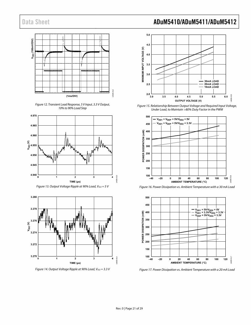
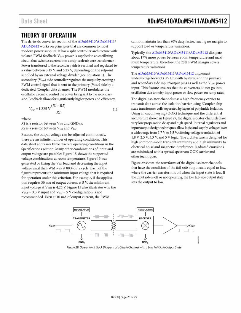
THEORY OF OPERATION The dc-to-dc converter section of the ADuM5410/ADuM5411/ ADuM5412 works on principles that are common to most modern power supplies. It has a split controller architecture with isolated PWM feedback. VDDP power is supplied to an oscillating circuit that switches current into a chip-scale air core transformer. Power transferred to the secondary side is rectified and regulated to a value between 3.15 V and 5.25 V, depending on the setpoint supplied by an external voltage divider (see Equation 1). The secondary (VISO) side controller regulates the output by creating a PWM control signal that is sent to the primary (VDDP) side by a dedicated iCoupler data channel. The PWM modulates the oscillator circuit to control the power being sent to the secondary side. Feedback allows for significantly higher power and efficiency.
R1
R2R1VISO
)(V225.1
(1)
where: R1 is a resistor between VSEL and GNDISO. R2 is a resistor between VSEL and VISO.
Because the output voltage can be adjusted continuously, there are an infinite number of operating conditions. This data sheet addresses three discrete operating conditions in the Specifications section. Many other combinations of input and output voltage are possible; Figure 15 shows the supported voltage combinations at room temperature. Figure 15 was generated by fixing the VISO load and decreasing the input voltage until the PWM was at 80% duty cycle. Each of the figures represents the minimum input voltage that is required for operation under this criterion. For example, if the applica-tion requires 30 mA of output current at 5 V, the minimum input voltage at VDDP is 4.25 V. Figure 15 also illustrates why the VDDP = 3.3 V input and VISO = 5 V configuration is not recommended. Even at 10 mA of output current, the PWM
cannot maintain less than 80% duty factor, leaving no margin to support load or temperature variations.
Typically, the ADuM5410/ADuM5411/ADuM5412 dissipate about 17% more power between room temperature and maxi-mum temperature; therefore, the 20% PWM margin covers temperature variations.
The ADuM5410/ADuM5411/ADuM5412 implement undervoltage lockout (UVLO) with hysteresis on the primary and secondary side input/output pins as well as the VDDP power input. This feature ensures that the converters do not go into oscillation due to noisy input power or slow power-on ramp rates.
The digital isolator channels use a high frequency carrier to transmit data across the isolation barrier using iCoupler chip scale transformer coils separated by layers of polyimide isolation. Using an on/off keying (OOK) technique and the differential architecture shown in Figure 29, the digital isolator channels have very low propagation delay and high speed. Internal regulators and input/output design techniques allow logic and supply voltages over a wide range from 1.7 V to 5.5 V, offering voltage translation of 1.8 V, 2.5 V, 3.3 V, and 5 V logic. The architecture is designed for high common-mode transient immunity and high immunity to electrical noise and magnetic interference. Radiated emissions are minimized with a spread spectrum OOK carrier and other techniques.
Figure 29 shows the waveforms of the digital isolator channels that have the condition of the fail-safe output state equal to low, where the carrier waveform is off when the input state is low. If the input side is off or not operating, the low fail-safe output state sets the output to low.
TRANSMITTER
GND1 GND2
VIN VOUT
RECEIVER
REGULATOR REGULATOR
1469
5-02
8
Figure 29. Operational Block Diagram of a Single Channel with a Low Fail-Safe Output State
APPLICATIONS INFORMATION PCB LAYOUT The ADuM5410/ADuM5411/ADuM5412 digital isolators with 0.15 W isoPower integrated dc-to-dc converters require no external interface circuitry for the logic interfaces. Power supply bypassing is required at the input and output supply pins (see Figure 32). Note that low ESR bypass capacitors of 0.01 μF to 0.1 μF value are required between the VDD1 pin and GND1 pin, and between the VDD2 pin and GNDISO pin, as close to the chip pads as possible, for proper operation of the data channels. The isoPower inputs require several passive components to bypass the power effectively, as well as set the output voltage and bypass the core voltage regulator (see Figure 30 through Figure 32).
PDIS
VDDP
GND110µF 0.1µF
+
10
11
12
1469
5-02
9
Figure 30. VDDP Bias and Bypass Components
VSEL
VISO OUT
ISO GND
FB2
GNDISO
VISO
0.1µF 10µF R110kΩ
R230kΩ
15
14
13
FB1
1469
5-03
0
Figure 31. VISO Bias and Bypass Components
The power supply section of the ADuM5410/ADuM5411/ ADuM5412 uses a 125 MHz oscillator frequency to efficiently pass power through its chip-scale transformers. Bypass capacitors are required for several operating frequencies. Noise suppression requires a low inductance, high frequency capacitor; ripple suppression and proper regulation require a large value capacitor. These capacitors are most conveniently connected between the VDDP pin and GND1 pin, and between the VISO pin and GNDISO pin. To suppress noise and reduce ripple, a parallel combination of at least two capacitors is required. The recommended capacitor values are 0.1 μF and 10 μF for VDD1. The smaller capacitor must have a low ESR; for example, use of a ceramic capacitor is advised. Note that the total lead length between the ends of the low ESR capacitor and the input power supply pin must not exceed 2 mm. Installing the bypass capacitor with traces more than 2 mm in length may result in data corruption.
To reduce the level of electromagnetic radiation, the impedance to high frequency currents between the VISO and GNDISO pins and the PCB trace connections can be increased. Using this method of EMI suppression controls the radiating signal at its source by placing surface-mount ferrite beads in series with the VISO and GNDISO pins, as seen in Figure 32. The impedance of the ferrite bead is chosen to be about 2 kΩ between the 100 MHz and 1 GHz frequency range, to reduce the emissions at the 125 MHz primary switching frequency and the 250 MHz secondary side rectifying frequency and harmonics. See Table 33 for examples of appropriate surface-mount ferrite beads. For additional reduction in emissions, PCB stitching capacitance can be implemented with a high voltage SMT safety capacitor. For optimal performance, it is important that the capacitor is connected directly between GND1 (Pin 12) and GNDISO (Pin 13), as shown in Figure 32.This capacitor is a SMT Size 1812, has a 3 kV voltage rating, and is manufactured by TDK Corporation (C4532C0G3F101K160KA).
Table 33. Surface-Mount Ferrite Beads Example Manufacturer Part No. Taiyo Yuden BKH1005LM182-T Murata Electronics BLM15HD182SN1
GNDISO
VSEL
NICNIC
VE2VE1/NIC
PDIS
VDDP VISO
0.1µF0.1µF
0.1µF
10µF FERRITES 10µFGND1 GNDISO
ADuM5410/ADuM5411/ADuM5412
GND1
VIB
VIA
VID/VOD
VIC/VOC
VOB
VOA
VOD/VID
VOC/VIC
VDD1 VDD2
GND1 GNDISO
1469
5-03
1
0.1µF
SMT 100pF SAFETY CAPACITORNIC = NO INTERNAL CONNECTION. LEAVE THIS PIN FLOATING.
Figure 32. Recommended PCB Layout
In applications involving high common-mode transients, ensure that board coupling across the isolation barrier is minimized. Furthermore, design the board layout such that any coupling that does occur equally affects all pins on a given component side. Failure to ensure these steps can cause voltage differentials between pins, exceeding the absolute maximum ratings specified in Table 26, thereby leading to latch-up and/or permanent damage.
THERMAL ANALYSIS The ADuM5410/ADuM5411/ADuM5412 consist of four internal die attached to a split lead frame with two die attach pads. For the purposes of thermal analysis, the die is treated as a thermal unit, with the highest junction temperature reflected in the θJA value from Table 21. The value of θJA is based on measurements taken with the devices mounted on a JEDEC standard, 4-layer board with fine width traces and still air. Under normal operating conditions, the ADuM5410/ADuM5411/ADuM5412 can operate at full load across the full temperature range without derating the output current.
PROPAGATION DELAY RELATED PARAMETERS Propagation delay is a parameter that describes the time it takes a logic signal to propagate through a component (see Figure 33). The propagation delay to a logic low output may differ from the propagation delay to a logic high.
INPUT (VIx)
OUTPUT (VOx)
tPLH tPHL
50%
50%14
695-
032
Figure 33. Propagation Delay Parameters
Pulse width distortion is the maximum difference between these two propagation delay values and is an indication of how accurately the input signal timing is preserved.
Channel to channel matching refers to the maximum amount the propagation delay differs between channels within a single ADuM5410/ADuM5411/ADuM5412 component.
Propagation delay skew refers to the maximum amount the propagation delay differs between multiple ADuM5410/ ADuM5411/ADuM5412 components operating under the same conditions.
EMI CONSIDERATIONS The dc-to-dc converter section of the ADuM5410/ADuM5411/ ADuM5412 components must, of necessity, operate at a very high frequency to allow efficient power transfer through the small transformers, which creates high frequency currents that can propagate in circuit board ground and power planes, causing edge and dipole radiation. Grounded enclosures are recommended for applications that use these devices. If grounded enclosures are not possible, follow good RF design practices in the layout of the PCB. Follow the layout techniques described in the PCB Layout section. See the AN-0971 Application Note for the most current PCB layout recommendations for the ADuM5410/ ADuM5411/ADuM5412.
POWER CONSUMPTION The VDDP power supply input only provides power to the converter. Power for the data channels is provided through VDD1 and VDD2. These power supplies can be connected to VDDP and VISO if desired, or the supplies can receive power from an independent source.
Treat the converter as a standalone supply to be utilized at the discretion of the designer.
The VDD1 or VDD2 supply current at a given channel of the ADuM5410/ADuM5411/ADuM5412 isolator is a function of the supply voltage, the data rate of the channel, and the output load of the channel.
To calculate the total VDD1 and VDD2 supply current, the supply currents for each input and output channel corresponding to VDD1 and VDD2 are calculated and totaled. Figure 18 and Figure 19 show per channel supply currents as a function of data rate for an unloaded output condition. Figure 20 shows the per channel supply current as a function of data rate for a 15 pF output condition. Figure 21 through Figure 26 show the total VDD1 and VDD2 supply current as a function of data rate for ADuM5410/ADuM5411/ADuM5412 channel configurations.
INSULATION LIFETIME All insulation structures eventually break down when subjected to voltage stress over a sufficiently long period. The rate of insulation degradation is dependent on the characteristics of the voltage waveform applied across the insulation as well as on the materials and material interfaces.
The two types of insulation degradation of primary interest are breakdown along surfaces exposed to the air and insulation wear out. Surface breakdown is the phenomenon of surface tracking and the primary determinant of surface creepage requirements in system level standards. Insulation wear out is the phenomenon where charge injection or displacement currents inside the insulation material cause long-term insulation degradation.
Surface Tracking
Surface tracking is addressed in electrical safety standards by setting a minimum surface creepage based on the working voltage, the environmental conditions, and the properties of the insulation material. Safety agencies perform characterization testing on the surface insulation of components that allows the components to be categorized in different material groups. Lower material group ratings are more resistant to surface tracking and, therefore, can provide adequate lifetime with smaller creepage. The minimum creepage for a given working voltage and material group is in each system level standard and is based on the total rms voltage across the isolation, pollution degree, and material group. The material group and creepage for the digital isolator channels are presented in Table 23.
Insulation Wear Out
The lifetime of insulation caused by wear out is determined by its thickness, material properties, and the voltage stress applied. It is important to verify that the product lifetime is adequate at the application working voltage. The working voltage supported by an isolator for wear out may not be the same as the working voltage supported for tracking. The working voltage applicable to tracking is specified in most standards.
Testing and modeling show that the primary driver of long-term degradation is displacement current in the polyimide insulation causing incremental damage. The stress on the insul-ation can be broken down into broad categories, such as dc stress, which causes very little wear out because there is no displacement current, and an ac component time varying voltage stress, which causes wear out.
The ratings in certification documents are usually based on 60 Hz sinusoidal stress because this reflects isolation from line voltage. However, many practical applications have combinations of 60 Hz ac and dc across the barrier as shown in Equation 1. Because only the ac portion of the stress causes wear out, the equation can be rearranged to solve for the ac rms voltage, as is shown in Equation 2. For insulation wear out with the polyimide materials used in these products, the ac rms voltage determines the product lifetime.
22DCRMSACRMS VVV (1)
or
22DCRMSRMSAC VVV (2)
where: VAC RMS is the time varying portion of the working voltage. VRMS is the total rms working voltage. VDC is the dc offset of the working voltage.
Calculation and Use of Parameters Example
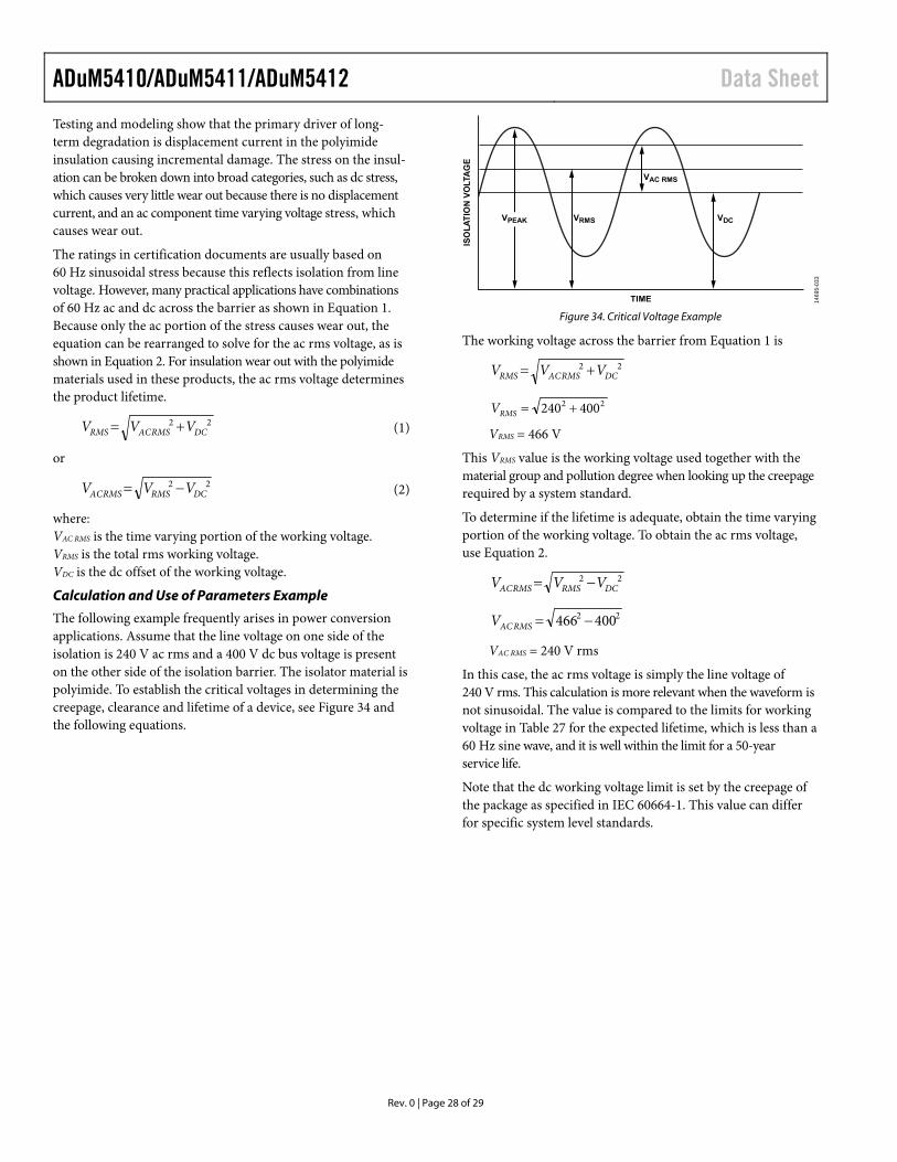
The following example frequently arises in power conversion applications. Assume that the line voltage on one side of the isolation is 240 V ac rms and a 400 V dc bus voltage is present on the other side of the isolation barrier. The isolator material is polyimide. To establish the critical voltages in determining the creepage, clearance and lifetime of a device, see Figure 34 and the following equations.
ISO
LA
TIO
N V
OLT
AG
E
TIME
VAC RMS
VRMS VDCVPEAK
1469
5-03
3
Figure 34. Critical Voltage Example
The working voltage across the barrier from Equation 1 is
22DCRMSACRMS VVV
22 400240 RMSV
VRMS = 466 V
This VRMS value is the working voltage used together with the material group and pollution degree when looking up the creepage required by a system standard.
To determine if the lifetime is adequate, obtain the time varying portion of the working voltage. To obtain the ac rms voltage, use Equation 2.
22DCRMSRMSAC VVV
22 400466 RMSACV
VAC RMS = 240 V rms
In this case, the ac rms voltage is simply the line voltage of 240 V rms. This calculation is more relevant when the waveform is not sinusoidal. The value is compared to the limits for working voltage in Table 27 for the expected lifetime, which is less than a 60 Hz sine wave, and it is well within the limit for a 50-year service life.
Note that the dc working voltage limit is set by the creepage of the package as specified in IEC 60664-1. This value can differ for specific system level standards.
Data Sheet ADuM5410/ADuM5411/ADuM5412
Rev. 0 | Page 29 of 29
OUTLINE DIMENSIONS
COMPLIANT TO JEDEC STANDARDS MO-150-AG 0601
06-A
24 13
121
8.508.207.90
8.207.807.40
5.605.305.00
SEATINGPLANE
0.05 MIN
0.65 BSC
2.00 MAX
0.380.22COPLANARITY
0.10
1.851.751.65
0.250.09
0.950.750.55
8°4°0°
Figure 35. 24-Lead Shrink Small Outline Package [SSOP]
EVAL-ADuM5411EBZ Evaluation Board2 EVAL-ADuM5411UEBZ Evaluation Board3 1 Z = RoHS Compliant Part. 2 The EVAL-ADuM5411EBZ is packaged with the ADuM5411BRSZ installed. 3 The EVAL-ADuM5411UEBZ is packaged without an ADuM5411 installed.