FEATURES D HIGH BANDWIDTH: 220MHz (G = +2) D HIGH OUTPUT CURRENT: ±85mA D LOW INPUT NOISE: 2.5nV/√Hz D LOW SUPPLY CURRENT: 5.7mA/ch D FLEXIBLE SUPPLY VOLTAGE: ±2V to ±6.3V Dual Supply +4V to +12.6V Single Supply D EXCELLENT DC ACCURACY: Maximum 25°C Input Offset Voltage = 0.8mV Maximum 25°C Input Offset Current = 500nA APPLICATIONS D LOW-COST VIDEO LINE DRIVERS D ADC PREAMPS D ACTIVE FILTERS D LOW-NOISE INTEGRATORS D PORTABLE TEST EQUIPMENT D OPTICAL CHANNEL AMPLIFIERS D LOW-POWER, BASEBAND AMPLIFIERS D CCD IMAGING CHANNEL AMPLIFIERS D OPA4650 UPGRADE DESCRIPTION The OPA4820 provides a wideband, unity-gain stable, voltage-feedback amplifier with a very low input noise voltage and high output current using a low 5.7mA/ch supply current. At unity-gain, the OPA4820 gives > 600MHz bandwidth with < 1 dB peaking. The OPA4820 complements this high-speed operation with excellent DC precision in a low-power device. A worst-case input offset voltage of ±0.8mV and an offset current of ±500nA give excellent absolute DC precision for pulse amplifier applications. Minimal input and output voltage swing headroom allow the OPA4820 to operate on a single +5V supply with > 2V PP output swing. While not a rail-to-rail (RR) output, this swing will support most emerging analog-to-digital converter (ADC) input ranges with lower power and noise than typical RR output op amps. Exceptionally low dG/dP (0.01%/0.03°) supports low-cost composite video line driver applications. Existing designs can use the industry-standard quad pinout SO-14 package while emerging high-density portable applications can use the TSSOP-14. RELATED PRODUCTS SINGLES DUALS TRIPLES QUADS FEATURES OPA354 OPA2354 — OPA4354 CMOS RR Output OPA690 OPA2690 OPA3690 — High Slew Rate — OPA2652 — — SOT23-8 — OPA2822 — — Low-Noise OPA820 — — — Single Channel Low-Noise Transceiver Interface OPA4820 SBOS317D - SEPTEMBER 2004 - REVISED AUGUST 2008 Quad, Unity-Gain Stable, Low-Noise, Voltage-Feedback Operational Amplifier PRODUCTION DATA information is current as of publication date. Products conform to specifications per the terms of Texas Instruments standard warranty. Production processing does not necessarily include testing of all parameters. www.ti.com Copyright 2004-2008, Texas Instruments Incorporated Please be aware that an important notice concerning availability, standard warranty, and use in critical applications of Texas Instruments semiconductor products and disclaimers thereto appears at the end of this data sheet. All trademarks are the property of their respective owners. +12V 1/4 OPA4820 AFE 1/4 OPA4820 402Ω 402Ω 133Ω 10kΩ Transmit Filter 10kΩ 50Ω 1:1 100Ω Line 10dBm 3.5 Crest Factor 50Ω 2V PP +6V Receiver Filter 1/4 OPA4820 1/4 OPA4820 402Ω 402Ω 14VPP VCM V CM 800Ω 800Ω 402Ω 402Ω VCM
Transcript
FEATURES HIGH BANDWIDTH: 220MHz (G = +2) HIGH OUTPUT CURRENT: ±85mA LOW INPUT NOISE: 2.5nV/ √Hz LOW SUPPLY CURRENT: 5.7mA/ch FLEXIBLE SUPPLY VOLTAGE:
±2V to ±6.3V Dual Supply+4V to +12.6V Single Supply
EXCELLENT DC ACCURACY:Maximum 25 °C Input Offset Voltage = 0.8mVMaximum 25 °C Input Offset Current = 500nA
APPLICATIONS LOW-COST VIDEO LINE DRIVERS ADC PREAMPS ACTIVE FILTERS LOW-NOISE INTEGRATORS PORTABLE TEST EQUIPMENT OPTICAL CHANNEL AMPLIFIERS LOW-POWER, BASEBAND AMPLIFIERS CCD IMAGING CHANNEL AMPLIFIERS OPA4650 UPGRADE
DESCRIPTIONThe OPA4820 provides a wideband, unity-gain stable,voltage-feedback amplifier with a very low input noisevoltage and high output current using a low 5.7mA/chsupply current. At unity-gain, the OPA4820 gives> 600MHz bandwidth with < 1 dB peaking. The OPA4820complements this high-speed operation with excellent DCprecision in a low-power device. A worst-case input offsetvoltage of ±0.8mV and an offset current of ±500nA giveexcellent absolute DC precision for pulse amplifierapplications.
Minimal input and output voltage swing headroom allowthe OPA4820 to operate on a single +5V supply with> 2VPP output swing. While not a rail-to-rail (RR) output,this swing will support most emerging analog-to-digitalconverter (ADC) input ranges with lower power and noisethan typical RR output op amps.
Exceptionally low dG/dP (0.01%/0.03°) supports low-costcomposite video line driver applications. Existing designscan use the industry-standard quad pinout SO-14 packagewhile emerging high-density portable applications can usethe TSSOP-14.
RELATED PRODUCTSSINGLES DUALS TRIPLES QUADS FEATURES
Please be aware that an important notice concerning availability, standard warranty, and use in critical applications of Texas Instrumentssemiconductor products and disclaimers thereto appears at the end of this data sheet.
All trademarks are the property of their respective owners.
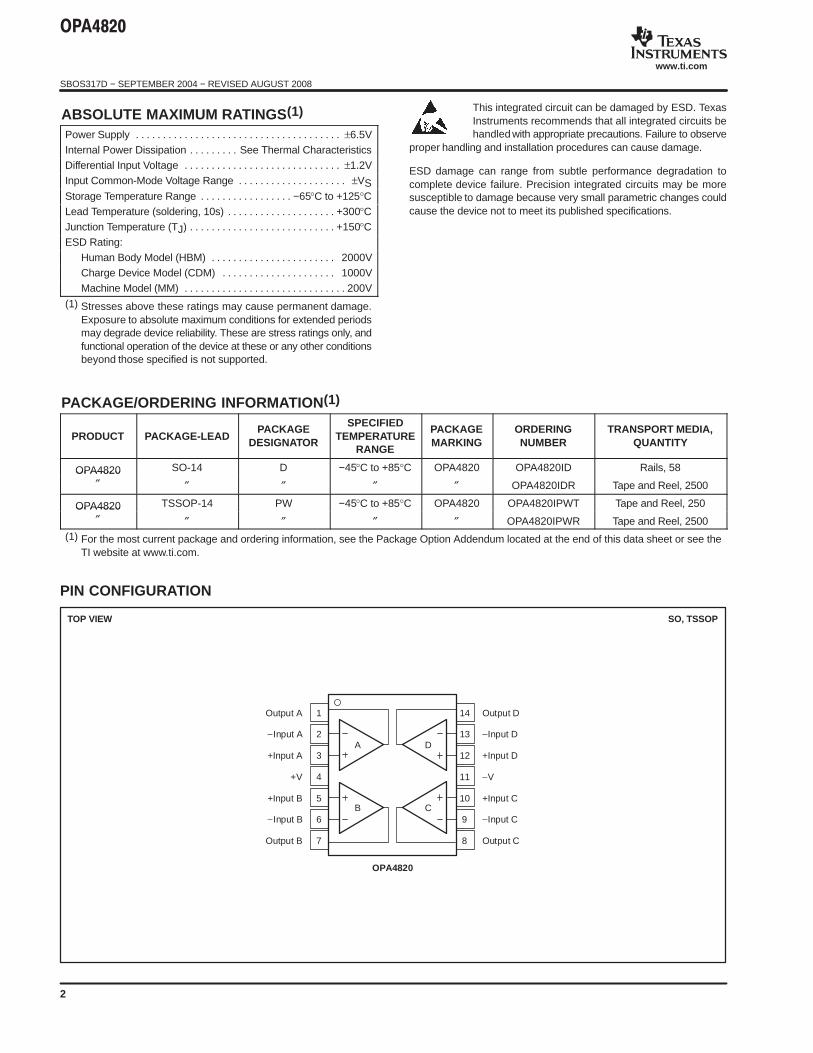
(1) Stresses above these ratings may cause permanent damage.Exposure to absolute maximum conditions for extended periodsmay degrade device reliability. These are stress ratings only, andfunctional operation of the device at these or any other conditionsbeyond those specified is not supported.
This integrated circuit can be damaged by ESD. TexasInstruments recommends that all integrated circuits behandled with appropriate precautions. Failure to observe
proper handling and installation procedures can cause damage.
ESD damage can range from subtle performance degradation tocomplete device failure. Precision integrated circuits may be moresusceptible to damage because very small parametric changes couldcause the device not to meet its published specifications.
PACKAGE/ORDERING INFORMATION (1)
PRODUCT PACKAGE-LEADPACKAGE
DESIGNATOR
SPECIFIEDTEMPERATURE
RANGE
PACKAGEMARKING
ORDERINGNUMBER
TRANSPORT MEDIA,QUANTITY
OPA4820 SO-14 D −45°C to +85°C OPA4820 OPA4820ID Rails, 58OPA4820″ ″ ″ ″ ″ OPA4820IDR Tape and Reel, 2500
OPA4820 TSSOP-14 PW −45°C to +85°C OPA4820 OPA4820IPWT Tape and Reel, 250OPA4820″ ″ ″ ″ ″ OPA4820IPWR Tape and Reel, 2500
(1) For the most current package and ordering information, see the Package Option Addendum located at the end of this data sheet or see theTI website at www.ti.com.
PIN CONFIGURATION
TOP VIEW SO, TSSOP
1
2
3
4
5
6
7
14
13
12
11
10
9
8
Output D
−Input D
+Input D
−V
+Input C
−Input C
Output C
Output A
−Input A
+Input A
+V
+Input B
−Input B
Output B
A D
B C
OPA4820
"#$%
SBOS317D − SEPTEMBER 2004 − REVISED AUGUST 2008
www.ti.com
3
ELECTRICAL CHARACTERISTICS: V S = ±5V Boldface limits are tested at +25°C.At RF = 402Ω, RL = 100Ω, and GND = +2, unless otherwise noted.
OPA4820ID, IPW
TYP MIN/MAX OVER TEMPERATURE
PARAMETER CONDITIONS +25°C +25°C(1)0°C to70°C(2)
−40°C to+85°C(2) UNITS
MIN/MAX
TESTLEVEL(3)
AC PERFORMANCESmall-Signal Bandwidth G = +1, VO = 0.1VPP, RF = 25Ω 650 MHz typ C
G = +2, VO = 0.1VPP 220 150 140 135 MHz min B
G = +10, VO = 0.1VPP 27 21 19 18 MHz min B
Gain-Bandwidth Product G ≥ 20 250 200 185 180 MHz min B
Peaking at a Gain of 1 VO = 0.1VPP, RF = 25Ω 1 dB typ C
Bandwidth for 0.1dB Gain Flatness G = +2, VO = 0.1VPP 33 MHz typ C
Large-Signal Bandwidth G = +2, 2VPP 80 MHz typ C
Slew Rate G = +2, 2V Step 240 190 184 178 V/µs min B
Rise Time and Fall TIme G = +2, VO = 2V Step 1.5 ns typ C
Settling Time to 0.02% G = +2, VO = 2V Step 22 ns typ C
Settling Time to 0.1% G = +2, VO = 2V Step 18 ns typ C
Harmonic Distortion G = +2, f = 1MHz, VO = 2VPP
2nd-Harmonic RL = 200Ω −84 −80 −79 −78 dBc max B
RL ≥ 500Ω −90 −85 −83 −81 dBc max B
3rd-Harmonic RL = 200Ω −92 −87 −86 −85 dBc max B
RL ≥ 500Ω −105 −100 −97 −95 dBc max B
Input Voltage Noise f > 100kHz 2.5 2.7 2.8 2.9 nV/√Hz max B
Noninverting Input Current Noise f > 100kHz 1.7 2.6 2.8 3.0 pA/√Hz max B
Differential Gain G = +2, NTSC, VO = 1.4VPP, RL = 150Ω 0.003 % typ C
Differential Phase G = +2, NTSC, VO = 1.4VPP, RL = 150Ω 0.06 ° typ C
All Hostile Crosstalk, Input-Referred3 Channels Driven at 5MHz, 1VPP
4th Channel Measured−61 dB typ C
DC PERFORMANCE(4)
Open-Loop Voltage Gain (AOL) VO = 0V, RL = 100Ω 66 62 61 60 dB min A
Input Offset Voltage VCM = 0V ±0.25 ±0.8 ±1.2 ±1.5 mV max A
Average Input Offset Voltage Drift VCM = 0V 8 10 µV/°C max B
Input Bias Current VCM = 0V −9 −20 −22 −26 µA max A
Average Input Bias Current Drift VCM = 0V 30 50 nA/°C max B
Input Offset Current VCM = 0V ±100 ±500 ±800 ±900 nA max A
Inverting Input Bias Current Drift VCM = 0V 5 5 nA/°C max B
INPUTCommon-Mode Input Range (CMIR)(5) ±4.0 ±3.8 ±3.7 ±3.6 V min A
Common-Mode Rejection Ratio (CMRR) VCM = 0V, Input-Referred 85 76 75 73 dB min A
Input Impedance, Differential Mode VCM = 0V 18 0.8 kΩ pF typ C
Input Impedance, Common-Mode VCM = 0V 6 1.0 MΩ pF typ C
OUTPUTOutput Voltage Swing RL ≥ 500Ω ±3.7 ±3.5 ±3.45 ±3.4 V min A
RL = 100Ω ±3.6 ±3.5 ±3.45 ±3.4 V min A
Output Current VO = 0 ±85 ±70 ±65 ±60 mA min A
Short-Circuit Output Current Output Shorted to Ground ±110 mA typ C
Closed-Loop Output Impedance G = +2, f ≤ 100kHz 0.04 Ω typ C
POWER SUPPLYSpecified Operating Voltage ±5 V typ C
Maximum Operating Voltage ±6.3 ±6.3 ±6.3 V max A
Minimum Operating Voltage ±2 V typ C
Maximum Quiescent Current VS = ±5V 22.6 23.4 25 25.8 mA max A
Minimum Quiescent Current VS = ±5V 22.6 21.8 20.2 19.4 mA min A
Power-Supply Rejection Ratio (−PSRR) Input-Referred 72 64 63 62 dB min A
THERMAL CHARACTERISTICSSpecification: ID, IPW −40 to +85 °C typ C
Thermal Resistance, JA
D SO-14 Junction-to-Ambient 100 °C/W typ C
PW TSSOP-14 Junction-to-Ambient 110 °C/W typ C
(1) Junction temperature = ambient for +25°C specifications.(2) Junction temperature = ambient at low temperature limits; junction temperature = ambient +28°C at high temperature limit for over temperature specifications.(3) Test levels: (A) 100% tested at +25°C. Over temperature limits by characterization and simulation. (B) Limits set by characterization and simulation. (C) Typical value only
for information.(4) Current is considered positive out of pin.(5) Tested < 3dB below minimum specified CMRR at ± CMIR limits.
"#$%
SBOS317D − SEPTEMBER 2004 − REVISED AUGUST 2008
www.ti.com
4
ELECTRICAL CHARACTERISTICS: V S = +5V Boldface limits are tested at +25°C.At RF = 402Ω, RL = 100Ω to 2.5V, and G = +2, unless otherwise noted.
OPA4820ID, IPW
TYP MIN/MAX OVER TEMPERATURE TEST
PARAMETER CONDITIONS +25°C +25°C(1)0°C to70°C(2)
−40°C to+85°C(2) UNITS
MIN/MAX
TESTLEVEL
(3)
AC PERFORMANCESmall-Signal Bandwidth G = +1, VO = 0.1VPP, RF = 25Ω 520 MHz typ C
G = +2, VO = 0.1VPP 210 148 135 130 MHz min B
G = +10, VO = 0.1VPP 25 18 17 16 MHz min B
Gain-Bandwidth Product G ≥ 20 230 180 170 160 MHz min B
Peaking at a Gain of 1 VO = 0.1VPP, RF = 25Ω 2 dB typ C
Large-Signal Bandwidth G = +2, VO = 2VPP 67 MHz typ C
Slew Rate G = +2, VO = 2V Step 190 135 130 125 V/µs min B
Rise Time and Fall Time G = +2, VO = 2V Step 1.8 ns typ C
Settling Time to 0.02% G = +2, VO = 2V Step 25 ns typ C
Settling Time to 0.1% G = +2, VO = 2V Step 22 ns typ C
Harmonic Distortion G = +2, f = 1MHz, VO = 2VPP
2nd-Harmonic RL = 200Ω −79 −75 −74 −73 dBc max B
RL ≥ 500Ω −83 −79 −77 −75 dBc max B
3rd-Harmonic RL = 200Ω −94 −87 −86 −85 dBc max B
RL ≥ 500Ω −98 −95 −93 −92 dBc max B
Input Voltage Noise f > 100kHz 2.5 2.8 2.9 3.0 nV/√Hz max B
Noninverting Input Current Noise f > 100kHz 1.6 2.5 2.7 2.9 pA/√Hz max B
All Hostile Crosstalk, Input-Referred3 Channels Driven at 5MHz, 1VPP
4th Channel Measured−61 dB typ C
DC PERFORMANCE(4)
Open-Loop Voltage Gain (AOL) VO = 2.5V, RL = 100Ω 65 60 59 58 dB min A
Input Offset Voltage VCM = 2.5V ±0.35 ±1.3 ±1.7 ±2.0 mV max A
Average Input Offset Voltage Drift VCM = 2.5V 8 10 µV/°C max B
Input Bias Current VCM = 2.5V −8 −18 −20 −24 µA max A
Average Input Bias Current Drift VCM = 2.5V 30 50 nA/°C max B
Input Offset Current VCM = 2.5V ±100 ±500 ±800 ±900 µA max A
Inverting Input Bias Current Drift VCM = 2.5V 5 5 nA/°C max B
INPUTLeast Positive Input Voltage 0.9 1.1 1.2 1.3 V min A
Most Positive Input Voltage 4.4 4.1 4.0 3.9 V max A
Common-Mode Rejection Ratio (CMRR)(5) VCM = 2.5V, Input-Referred 83 74 73 72 dB min A
Input Impedance, Differential-Mode VCM = 2.5V 15 1 kΩ pF typ C
Input Impedance, Common-Mode VCM = 2.5V 5 1.3 MΩ pF typ C
OUTPUTLeast Positive Output Voltage RL ≥ 500Ω to 2.5V 3.9 3.8 3.75 3.7 V min A
RL = 100Ω to 2.5V 3.8 3.7 3.65 3.6 V min A
Most Negative Output Voltage RL ≥ 500Ω to 2.5V 1.2 1.3 1.35 1.4 V min A
RL = 100Ω to 2.5V 1.2 1.3 1.35 1.4 V min A
Output Current VO = 2.5V ±75 ±60 ±55 ±50 mA min A
Short-Circuit Output Current Output Shorted to Ground ±105 mA typ C
Closed-Loop Output Impedance G = +2, f ≤ 100kHz 0.04 Ω typ C
POWER SUPPLYSpecified Operating Voltage +5 V typ C
Maximum Operating Voltage +12.6 +12.6 +12.6 V max A
Minimum Operating Voltage +4 V typ C
Maximum Quiescent Current VS = +5V, 4 Channels 20.4 22.2 22.6 23.0 mA max A
Minimum Quiescent Current VS = +5V, 4 Channels 20.4 18.0 17.4 16.8 mA min A
Power-Supply Rejection Ratio (+PSRR) Input-Referred 68 dB typ C
THERMAL CHARACTERISTICSSpecification: ID, IPW −40 to +85 °C typ C
Thermal Resistance, JA
D SO-14 Junction-to-Ambient 100 °C/W typ C
PW TSSOP-14 Junction-to-Ambient 110 °C/W typ C(1) Junction temperature = ambient for +25°C specifications.(2) Junction temperature = ambient at low temperature limits; junction temperature = ambient +13°C at high temperature limit for over temperature.(3) Test levels: (A) 100% tested at +25°C. Over temperature limits by characterization and simulation. (B) Limits set by characterization and simulation. (C) Typical value only
for information.(4) Current considered positive out of pin.(5) Tested < 3dB below minimum specified CMRR at ± CMIR limits.
"#$%
SBOS317D − SEPTEMBER 2004 − REVISED AUGUST 2008
www.ti.com
5
TYPICAL CHARACTERISTICS: V S = ±5V
RF = 402Ω, RL = 100Ω, and G = +2, unless otherwise noted.
3
0
−3
−6
−9
−12
−15
−18
NONINVERTING SMALL−SIGNAL FREQUENCY RESPONSE
Frequency (Hz)
Nor
mal
ized
Ga
in(d
B)
1M 10M 100M 1G
G = +1, RF = 25Ω
G = +2G = +5
G = +10
VO = 0.1VPPRL = 100ΩSee Figure 1
9
6
3
0
−3
−6
−9
−12
NONINVERTING LARGE−SIGNAL FREQUENCY RESPONSE
Frequency (MHz)
Gai
n(d
B)
1 10 100 500
VO = 1VPP
VO = 0.5VPP
VO = 2VPP
VO = 4VPP
G = +2V/VRL = 100ΩSee Figure 1
0.4
0.3
0.2
0.1
0
−0.1
−0.2
−0.3
−0.4
NONINVERTING PULSE RESPONSE
Time (10ns/div)
Sm
all−
Sig
nalO
utpu
tVol
tage
(100
mV
/div
) 2.0
1.5
1.0
0.5
0
−0.5
−1.0
−1.5
−2.0 Larg
e−S
igna
lOut
putV
olta
ge(5
00m
V/d
iv)
Large−Signal ± 1VRight Scale
Small−Signal ± 100mVLeft Scale
G = +2V/VSee Figure 1
3
0
−3
−6
−9
−12
−15
−18
INVERTING SMALL−SIGNAL FREQUENCY RESPONSE
Frequency (MHz)
Nor
mal
ized
Ga
in(d
B)
1 10 100 500
G = −1
G = −2G = −5
G = −10
VO = 0.1VPPRL = 100ΩSee Figure 2
3
0
−3
−6
−9
−12
−15
−18
INVERTING LARGE−SIGNAL FREQUENCY RESPONSE
Frequency (MHz)
Gai
n(d
B)
1 10 100 500
VO = 1VPP
VO = 0.5VPP
VO = 2VPP
VO = 4VPP
G = −1V/VRL = 100ΩSee Figure 2
0.4
0.3
0.2
0.1
0
−0.1
−0.2
−0.3
−0.4
INVERTING PULSE RESPONSE
Time (10ns/div)
Sm
all−
Sig
nalO
utpu
tVol
tage
(100
mV
/div
) 2.0
1.5
1.0
0.5
0
−0.5
−1.0
−1.5
−2.0 Larg
e−S
igna
lOut
putV
olta
ge(5
00m
V/d
iv)
Large−Signal ± 1VRight Scale
Small−Signal ± 100mVLeft Scale
G = −1V/VSee Figure 2
"#$%
SBOS317D − SEPTEMBER 2004 − REVISED AUGUST 2008
www.ti.com
6
TYPICAL CHARACTERISTICS: V S = ±5V (continued)
RF = 402Ω, RL = 100Ω, and G = +2, unless otherwise noted.
−60
−65
−70
−75
−80
−85
−90
−95
−100
−105
HARMONIC DISTORTION vs LOAD RESISTANCE
Resistance (Ω)
Har
mon
icD
isto
rtio
n(d
Bc)
100 1000
G = +2V/Vf = 1MHzVO = 2VPP
2nd−Harmonic
3rd−Harmonic
−60
−65
−70
−75
−80
−85
−90
−95
−100
−105
HARMONIC DISTORTION vs FREQUENCY
Frequency (MHz)
Har
mon
icD
isto
rtio
n(d
Bc)
0.1 1 10
3rd−Harmonic
2nd−Harmonic
G = +2V/VVO = 2VPPRL = 200ΩSee Figure 1
−70
−75
−80
−85
−90
−95
−100
−105
−110
HARMONIC DISTORTION vs NONINVERTING GAIN
Gain (V/V)
Har
mon
icD
isto
rtio
n(d
Bc)
1 10
f = 1MHzRL = 200ΩVO = 2VPPSee Figure 1
2nd−Harmonic
3rd−Harmonic
−60
−65
−70
−75
−80
−85
−90
−95
−100
−105
1MHz HARMONIC DISTORTION vs SUPPLY VOLTAGE
Supply Voltage (±VS)
Har
mon
icD
isto
rtio
n(d
Bc)
2.5 3.0 3.5 4.0 4.5 5.0 5.5 6.0
G = +2V/VRL = 200ΩVO = 2VPPSee Figure 1
2nd−Harmonic
3rd−Harmonic
−60
−65
−70
−75
−80
−85
−90
−95
−100
−105
HARMONIC DISTORTION vs OUTPUT VOLTAGE
Output Voltage Swing (VPP)
Har
mon
icD
isto
rtio
n(d
Bc)
0.1 1 10
G = +2V/Vf = 1MHzRL = 200ΩSee Figure 1
2nd−Harmonic
3rd−Harmonic
−70
−75
−80
−85
−90
−95
−100
−105
−110
HARMONIC DISTORTION vs INVERTING GAIN
Gain ( V/V )
Har
mon
icD
isto
rtio
n(d
Bc)
1 10
f = 1MHzRL = 200ΩVO = 2VPPSee Figure 2
2nd−Harmonic
3rd−Harmonic
"#$%
SBOS317D − SEPTEMBER 2004 − REVISED AUGUST 2008
www.ti.com
7
TYPICAL CHARACTERISTICS: V S = ±5V (continued)
RF = 402Ω, RL = 100Ω, and G = +2, unless otherwise noted.
100
10
1
INPUT VOLTAGE AND CURRENT NOISE
Frequency (Hz)
10 100 1k 10k 100k 1M 10M
Vo
ltage
No
ise
(nV
/√H
z)C
urre
ntN
ois
e(p
A/√
Hz)
Voltage Noise (2.5nV/√Hz)
Current Noise (1.7pA/√Hz)
100
10
1
RECOMMENDED RS vs CAPACITIVE LOAD
Capacitive Load (pF)
1 10 100 1000
RS
(Ω)
0.1dB Peaking Targeted
90
80
70
60
50
40
30
20
10
0
CMRR AND PSRR vs FREQUENCY
Frequency (Hz)
Com
mo
n−M
ode
Re
ject
ion
Ra
tio(d
B)
Pow
er−
Sup
ply
Rej
ectio
nR
atio
(dB
)
1k 10k 100k 1M 10M 100M
CMRR
+PSRR
−PSRR
45
40
35
30
25
20
15
TWO−TONE, 3RD−ORDERINTERMODULATION INTERCEPT
Frequency (MHz)
Inte
rcep
tPoi
nt(+
dBm
)
0 5 10 15 20 25 30
402Ω
1 /4
O P A 4 8 2 0
PI
PO50Ω200Ω
402Ω
8
7
6
5
4
3
2
1
0
−1
−2
−3
FREQUENCY RESPONSE vs CAPACITIVE LOAD
Frequency (MHz)
No
rmal
ize
dG
ain
toC
apac
itive
Loa
d(d
B)
1 10 100 400
CL = 10pF
CL = 22pF
CL = 47pF
CL = 100pF
402Ω
RS
OPA4820
VI
VO50Ω
1kΩ(1)CL
402ΩNOTE: (1) 1kΩ is optional.
80
70
60
50
40
30
20
10
0
−10
OPEN−LOOP GAIN AND PHASE
Frequency (Hz)
Ope
n−Lo
opG
ain
(dB
)
0
−20
−40
−60
−80
−100
−120
−140
−160
−180
Ope
n−Lo
opP
hase
()
100 1k 10k 100k 1M 10M 100M 1G
20 log (AOL)
∠AOL
"#$%
SBOS317D − SEPTEMBER 2004 − REVISED AUGUST 2008
www.ti.com
8
TYPICAL CHARACTERISTICS: V S = ±5V (continued)
RF = 402Ω, RL = 100Ω, and G = +2, unless otherwise noted.
5
4
3
2
1
0
−1
−2
−3
−4
−5
OUTPUT VOLTAGE AND CURRENT LIMITATIONS
IO (mA)
VO
(V)
−150 −100 −50 0 50 100 150
RL = 100Ω
RL = 25Ω
RL = 50Ω
1W Internal
Power Limit
Output Current
Limit
Output Current
Limit
1W Internal
Power LimitSingle Channel
8
6
4
2
0
−2
−4
−6
−8
NONINVERTING OVERDRIVE RECOVERY
Time (40ns/div)
Out
putV
olta
ge
(2V
/div
)
4
3
2
1
0
−1
−2
−3
−4
Inpu
tVol
tage
(1V
/div
)
Input Right Scale
Output Left Scale
RL = 100ΩG = +2V/VSee Figure 1
0.20
0.18
0.16
0.14
0.12
0.10
0.08
0.06
0.04
0.02
0
COMPOSITE VIDEO dG/dP
Video Loads
Diff
eren
tialG
ain
(%)
0.40
0.36
0.32
0.28
0.24
0.20
0.16
0.12
0.08
0.04
0
Diff
eren
tialP
hase
()
1 2 3 4
dG Negative Video
dG Positive Video
dP Negative VideodP Positive Video
G = +2V/V
10
1
0.1
0.01
CLOSED−LOOP OUTPUT IMPEDANCE vs FREQUENCY
Frequency (Hz)
1k 10k 100k 1M 10M 100M
Out
putI
mpe
dan
ce(Ω
)
5
4
3
2
1
0
−1
−2
−3
−4
−5
INVERTING OVERDRIVE RECOVERY
Time (40ns/div)
Inp
ut/O
utp
utV
olta
ge(1
V/d
iv)
Input
OutputRL = 100ΩG = −1V/V
See Figure 2
1.0
0.5
0
−0.5
−1.0
TYPICAL DC DRIFT OVER TEMPERATURE
Ambient Temperature (C)
Inpu
tOffs
etV
olta
ge(m
V)
20
10
0
−10
−20
Inpu
tBia
san
dO
ffset
Cur
rent
(µA
)
−50 −25 0 25 50 75 100 125
Input Offset Voltage (VOS)Left Scale
10x Input Offset Current (IOS)Right Scale
Input Bias Current (IB)Right Scale
"#$%
SBOS317D − SEPTEMBER 2004 − REVISED AUGUST 2008
www.ti.com
9
TYPICAL CHARACTERISTICS: V S = ±5V (continued)
RF = 402Ω, RL = 100Ω, and G = +2, unless otherwise noted.
110
100
90
80
70
SUPPLY AND OUTPUT CURRENT vs TEMPERATURE
Ambient Temperature (C)
Out
putC
urre
nt(1
0mA
/div
)
26
24
22
20
18
Sup
ply
Cur
rent
(2m
A/d
iv)
−50 −25 0 25 50 75 100 125
Sourcing Output CurrentLeft Scale
Total Supply CurrentRight Scale
Sinking Output CurrentLeft Scale
10M
1M
100k
10k
1k
COMMON−MODE AND DIFFERENTIALINPUT IMPEDANCE
Frequency (Hz)
Inpu
tIm
ped
ance
(Ω)
100 1k 10k 100k 1M 10M 100M
Common−Mode Input Impedance
Differential Input Impedance
6
5
4
3
2
1
0
COMMON−MODE INPUT RANGE AND OUTPUT SWINGvs SUPPLY VOLTAGE
Supply Voltage (±VS)
Vo
ltage
Ran
ge
(V)
2.5 3.0 3.5 4.0 4.5 5.0 5.5 6.0
+VIN
−VIN
+VOUT
−VOUT
RL ≥ 500Ω
−10
−20
−30
−40
−50
−60
−70
−80
CROSSTALK vs FREQUENCY
Frequency (MHz)
Cro
ssta
lk(d
B)
1 10 100
All Hostile Crosstalk1VPP Output, 3 Channels, 100ΩLoad
RF = 402Ω, RL = 100Ω to VS/2, and G = +2, unless otherwise noted.
3
0
−3
−6
−9
−12
−15
−18
NONINVERTING SMALL−SIGNAL FREQUENCY RESPONSE
Frequency (MHz)
Nor
mal
ized
Ga
in(d
B)
1 10 100 600
G = +1, RF = 25Ω
G = +2G = +5
G = +10
VO = 0.1VPPRL = 100ΩSee Figure 3
9
6
3
0
−3
−6
−9
−12
NONINVERTING LARGE−SIGNAL FREQUENCY RESPONSE
Frequency (MHz)
Gai
n(d
B)
1 10 100 500
VO = 1VPP
VO = 0.5VPP
VO = 2VPP
VO = 3VPP
G = +2V/VRL = 100ΩSee Figure 3
0.4
0.3
0.2
0.1
0
−0.1
−0.2
−0.3
−0.4
NONINVERTING PULSE RESPONSE
Time (10ns/div)
Sm
all−
Sig
nalO
utpu
tVol
tage
(100
mV
/div
) 2.0
1.5
1.0
0.5
0
−0.5
−1.0
−1.5
−2.0 Larg
e−S
igna
lOut
putV
olta
ge(5
00m
V/d
iv)
Large−Signal ± 1VRight Scale
Small−Signal ± 100mVLeft Scale
G = +2V/VSee Figure 3
3
0
−3
−6
−9
−12
−15
−18
INVERTING SMALL−SIGNAL FREQUENCY RESPONSE
Frequency (MHz)
Nor
mal
ized
Ga
in(d
B)
1 10 100 500
G = −2
G = −1
G = −5
G = −10
VO = 0.1VPPRL = 100ΩSee Figure 4
3
0
−3
−6
−9
−12
−15
−18
INVERTING LARGE−SIGNAL FREQUENCY RESPONSE
Frequency (MHz)
Gai
n(d
B)
1 10 100 500
VO = 1VPP
VO = 0.5VPP
VO = 2VPP
VO = 3VPP
G = −1V/VRL = 100ΩSee Figure 4
0.4
0.3
0.2
0.1
0
−0.1
−0.2
−0.3
−0.4
INVERTING PULSE RESPONSE
Time (10ns/div)
Sm
all−
Sig
nalO
utpu
tVol
tage
(100
mV
/div
) 2.0
1.5
1.0
0.5
0
−0.5
−1.0
−1.5
−2.0 Larg
e−S
igna
lOut
putV
olta
ge(5
00m
V/d
iv)
Large−Signal ± 1VRight Scale
Small−Signal ± 100mVLeft Scale
G = −1V/VSee Figure 4
"#$%
SBOS317D − SEPTEMBER 2004 − REVISED AUGUST 2008
www.ti.com
11
TYPICAL CHARACTERISTICS: V S = +5V (continued)
RF = 402Ω, RL = 100Ω to VS/2, and G = +2, unless otherwise noted.
−60
−65
−70
−75
−80
−85
−90
−95
−100
−105
HARMONIC DISTORTION vs LOAD RESISTANCE
Resistance (Ω)
Ha
rmon
icD
isto
rtio
n(d
Bc)
100 1000
G = +2V/Vf = 1MHz
VO = 2VPP
2nd−Harmonic
3rd−Harmonic
−60
−65
−70
−75
−80
−85
−90
−95
−100
−105
HARMONIC DISTORTION vs OUTPUT VOLTAGE
Output Voltage Swing (VPP)
Har
mon
icD
isto
rtio
n(d
Bc)
0.1 1 10
G = +2V/Vf = 1MHzRL = 200ΩSee Figure 3
2nd−Harmonic
3rd−Harmonic
−60
−65
−70
−75
−80
−85
−90
−95
−100
−105
HARMONIC DISTORTION vs INVERTING GAIN
Gain ( V/V )
Ha
rmon
icD
isto
rtio
n(d
Bc)
1 10
f = 1MHzRL = 200ΩVO = 2VPPSee Figure 4
2nd−Harmonic
3rd−Harmonic
−60
−65
−70
−75
−80
−85
−90
−95
−100
−105
HARMONIC DISTORTION vs FREQUENCY
Frequency (MHz)
Ha
rmon
icD
isto
rtio
n(d
Bc)
0.1 1 10
G = +2V/VRL = 200ΩVO = 2VPP
2nd−Harmonic
3rd−Harmonic
−60
−65
−70
−75
−80
−85
−90
−95
−100
−105
HARMONIC DISTORTION vs NONINVERTING GAIN
Gain (V/V)
Ha
rmon
icD
isto
rtio
n(d
Bc)
1 10
f = 1MHzRL = 200ΩVO = 2VPPSee Figure 3
2nd−Harmonic
3rd−Harmonic
40
35
30
25
20
15
TWO−TONE, 3RD−ORDERINTERMODULATION INTERCEPT
Frequency (MHz)
Inte
rcep
tPoi
nt(+
dBm
)
0 5 10 15 20 25 30
402Ω
1/4OPA4820
PI
+5V
PO57.6Ω200Ω
0.1µF
806Ω
806Ω
402Ω
0.1µF
0.01µF
"#$%
SBOS317D − SEPTEMBER 2004 − REVISED AUGUST 2008
www.ti.com
12
TYPICAL CHARACTERISTICS: V S = +5V (continued)
RF = 402Ω, RL = 100Ω to VS/2, and G = +2, unless otherwise noted.
100
10
1
RECOMMENDED RS vs CAPACITIVE LOAD
Capacitive Load (pF)
1 10 100 1000
RS
(Ω)
0.1dB Peaking Targeted
1.5
1.0
0.5
0
−0.5
−1.0
−1.5
TYPICAL DC DRIFT OVER TEMPERATURE
Ambient Temperature (C)
Inpu
tOffs
etV
olta
ge(m
V)
15
10
5
0
−5
−10
−15
Impu
tBia
san
dO
ffset
Cur
rent
(µA
)
−50 −25 0 25 50 75 100 125
Input Offset Voltage (VOS)Left Scale
10x Input Offset Current (IOS)Right Scale
Input Bias Current (IB)Right Scale
8
7
6
5
4
3
2
1
0
−1
−2
−3
FREQUENCY RESPONSE vs CAPACITIVE LOAD
Frequency (MHz)
Nor
ma
lized
Gai
nto
Cap
aci
tive
Loa
d(d
B)
1 10 100 300
CL = 10pF
CL = 22pF
CL = 47pF
CL = 100pF
402Ω
RS
OPA820
VI
+5V
VO57.6Ω1kΩ(1)
806Ω
806Ω
CL
402Ω
0.01µF
0.01µF
NOTE: (1) 1kΩ is optional.
90
85
80
75
70
65
60
SUPPLY AND OUTPUT CURRENT vs TEMPERATURE
Ambient Temperature (C)
Out
put
Cur
rent
(5m
A/d
iv)
23
22
21
20
19
18
17
Sup
ply
Cur
rent
(1m
A/d
iv)
−50 −25 0 25 50 75 100 125
Sourcing Output CurrentLeft Scale
Total Supply CurrentRight Scale
Sinking Output CurrentLeft Scale
"#$%
SBOS317D − SEPTEMBER 2004 − REVISED AUGUST 2008
www.ti.com
13
APPLICATIONS INFORMATIONWIDEBAND VOLTAGE-FEEDBACKOPERATIONThe combination of speed and dynamic range offered bythe OPA4820 is easily achieved in a wide variety ofapplication circuits, providing that simple principles ofgood design are observed. For example, goodpower-supply decoupling, as shown in Figure 1, isessential to achieve the lowest possible harmonicdistortion and smooth frequency response.
Proper printed circuit board (PCB) layout and carefulcomponent selection will maximize the performance of theOPA4820 in all applications, as discussed in the followingsections of this data sheet.
Figure 1 shows the gain of +2 configuration used as thebasis for most of the Typical Characteristics. Most of thecurves were characterized using signal sources with 50Ωdriving impedance and with measurement equipmentpresenting 50Ω load impedance. In Figure 1, the 50Ωshunt resistor at the VI terminal matches the sourceimpedance of the test generator while the 50Ω seriesresistor at the VO terminal provides a matching resistor forthe measurement equipment load. Generally, data sheetspecifications refer to the voltage swings at the output pin(VO in Figure 1). The 100Ω load, combined with the 804Ωtotal feedback network load, presents the OPA4820 withan effective load of approximately 90Ω in Figure 1.
+5V
−5V−VS
+VS
RS50ΩVO
VIN 50Ω
+2.2µF
+
2.2µF
0.1µF
RG402Ω
RF402Ω
50Ω Source
50Ω Load
0.1µF
1/4OPA4820
Figure 1. Gain of +2, High-Frequency Applicationand Characterization Circuit
WIDEBAND INVERTING OPERATIONOperating the OPA4820 as an inverting amplifier hasseveral benefits and is particularly useful when a matched50Ω source and input impedance is required. Figure 2shows the inverting gain of −1 circuit used as the basis ofthe inverting mode Typical Characteristics.
+5V
−5V
50ΩVO
VI
+0.1µF 2.2µF
+
0.1µF 2.2µF
RM57.6Ω
RT205Ω
RF402Ω
50Ω Source
50Ω Load
0.01µF
RG402Ω
1/4OPA4820
Figure 2. Inverting G = −1 Specifications and TestCircuit
In the inverting case, just the feedback resistor appears aspart of the total output load in parallel with the actual load.For the 100Ω load used in the Typical Characteristics, thisgives a total load of 80Ω in this inverting configuration. Thegain resistor is set to get the desired gain (in this case402Ω for a gain of −1) while an additional input matchingresistor (RM) can be used to set the total input impedanceequal to the source if desired. In this case, RM = 57.6Ω inparallel with the 402Ω gain setting resistor gives amatched input impedance of 50Ω. This matching is onlyneeded when the input needs to be matched to a sourceimpedance, as in the characterization testing done usingthe circuit of Figure 2.The OPA4820 offers extremely good DC accuracy as well aslow noise and distortion. To take full advantage of that DCprecision, the total DC impedance looking out of each of theinput nodes must be matched to get bias currentcancellation. For the circuit of Figure 2, this requires the205Ω resistor shown to ground on the noninverting input. Thecalculation for this resistor includes a DC-coupled 50Ωsource impedance along with RG and RM. Although thisresistor will provide cancellation for the bias current, it mustbe well decoupled (0.01µF in Figure 2) to filter the noisecontribution of the resistor and the input current noise.As the required RG resistor approaches 50Ω at highergains, the bandwidth for the circuit in Figure 2 will farexceed the bandwidth at that same gain magnitude for thenoninverting circuit of Figure 1. This occurs due to thelower noise gain for the circuit of Figure 2 when the 50Ωsource impedance is included in the analysis. Forinstance, at a signal gain of −10 (RG = 50Ω, RM = open,RF = 499Ω) the noise gain for the circuit of Figure 2 willbe 1 + 499Ω/(50Ω + 50Ω) = 6 as a result of adding the 50Ωsource in the noise gain equation. This gives considerablehigher bandwidth than the noninverting gain of +10. Usingthe 240MHz gain bandwidth product for the OPA4820, aninverting gain of −10 from a 50Ω source to a 50Ω RG gives42MHz bandwidth, whereas the noninverting gain of +10gives 27MHz.
"#$%
SBOS317D − SEPTEMBER 2004 − REVISED AUGUST 2008
www.ti.com
14
WIDEBAND SINGLE-SUPPLY OPERATIONFigure 3 shows the AC-coupled, single +5V supply, gain of+2V/V circuit configuration used as a basis for the +5V onlyElectrical and Typical Characteristics. The key require-ment for single-supply operation is to maintain input andoutput signal swings within the useable voltage ranges atboth the input and the output. The circuit of Figure 3establishes an input midpoint bias using a simple resistivedivider from the +5V supply (two 806Ω resistors) to thenoninverting input. The input signal is then AC-coupledinto this midpoint voltage bias. The input voltage can swingto within 0.9V of the negative supply and 0.6V of thepositive supply, giving a 3.5VPP input signal range. Theinput impedance matching resistor (57.6Ω) used inFigure 3 is adjusted to give a 50Ω input match when theparallel combination of the biasing divider network isincluded. The gain resistor (RG) is AC-coupled, giving thecircuit a DC gain of +1. This puts the input DC bias voltage(2.5V) on the output as well. On a single +5V supply, theoutput voltage can swing to within 1.3V of either supply pin
while delivering more than 60mA output current giving2.4V output swing into 100Ω (5.6dBm maximum at amatched 50Ω load).
Figure 4 shows the AC-coupled, single +5V supply, gain of−1V/V circuit configuration used as a basis for the +5V onlyTypical Characteristic curves. In this case, the midpointDC bias on the noninverting input is also decoupled withan additional 0.01µF decoupling capacitor. This reducesthe source impedance at higher frequencies for thenoninverting input bias current noise. This 2.5V bias on thenoninverting input pin appears on the inverting input pinand, since RG is DC blocked by the input capacitor, willalso appear at the output pin.
The single-supply test circuits of Figure 3 and Figure 4show +5V operation. These same circuits can be usedover a single-supply range of +4V to +12.6V. Operating ona single +12V supply, with the Absolute Maximum Supplyvoltage specification of +13V, gives adequate designmargin for the typical ±5% supply tolerance.
+5V+VS
DIS100Ω
RG402Ω
806Ω
806Ω
57.6Ω
0.01µF
+
6.8µF0.1µF
0.01µFVI
50ΩSource
RF402Ω
VOVS/2
1/4OPA4820
Figure 3. AC-Coupled, G = +2V/V, Single-Supply Specifications and Test Circuit
+5V+VS
DIS100Ω
RG402Ω
806Ω
806Ω
0.01µF
0.01µF
VI
RF402Ω
VOVS/2
+
6.8µF0.1µF
1/4OPA4820
Figure 4. AC-Coupled, G = −1V/V, Single-Supply Specifications and Test Circuit
"#$%
SBOS317D − SEPTEMBER 2004 − REVISED AUGUST 2008
www.ti.com
15
DIFFERENTIAL INTERFACE APPLICATIONSDual and quad op amps are particularly suitable todifferential input to differential output applications.Typically, these fall into either ADC input interface or linedriver applications. Two basic approaches to differentialI/O are noninverting or inverting configurations. Since theoutput is differential, the signal polarity is somewhatmeaningless—the noninverting and inverting terminologyapplies here to where the input is brought into theOPA4820. Each has its advantages and disadvantages.Figure 5 shows a basic starting point for noninvertingdifferential I/O applications.
RF402Ω
RF402Ω
1/4OPA4820
+VCC
−VCC
RG VO
1/4OPA4820
VI
Figure 5. Noninverting Differential I/O Amplifier
This approach provides for a source terminationimpedance that is independent of the signal gain. Forinstance, simple differential filters may be included in thesignal path right up to the noninverting inputs withoutinteracting with the amplifier gain. The differential signalgain for the circuit of Figure 5 is:
VO
VI AD 1 2
RF
RG
Figure 5 shows the recommended value of 402Ω.However, the gain may be adjusted using just the RGresistor.
Various combinations of single-supply or AC-coupledgains can also be delivered using the basic circuit ofFigure 5. Common-mode bias voltages on the twononinverting inputs pass on to the output with a gain of 1since an equal DC voltage at each inverting node createsno current through RG, giving that voltage a common-mode gain of 1 to the output.
Figure 6 shows a differential I/O stage configured as aninverting amplifier. In this case, the gain resistors (RG)become the input resistance for the source. This providesa better noise performance than the noninvertingconfiguration, but does limit the flexibility in setting theinput impedance separately from the gain.
RF402Ω
RF402Ω
RG
RG
1/4OPA4820
+VCC
−VCC
VCM
VCM
VO
1/4OPA4820
VI
Figure 6. Inverting Differential I/O Amplifier
The two noninverting inputs provide an easycommon-mode control input. This is particularly useful ifthe source is AC-coupled through either blocking caps ora transformer. In either case, the common-mode inputvoltages on the two noninverting inputs again have a gainof 1 to the output pins, giving an easy common-modecontrol for single-supply operation. The input resistorsmay be adjusted to the desired gain but will also bechanging the input impedance as well. The differential gainfor this circuit is:
VO
VI
RF
RG
(1)
(2)
"#$%
SBOS317D − SEPTEMBER 2004 − REVISED AUGUST 2008
www.ti.com
16
DC-COUPLED SINGLE-TO-DIFFERENTIALCONVERSIONThe previous differential output circuits were set up toreceive a differential input as well as provide a differentialoutput. Figure 7 shows one way to provide a single todifferential conversion, with DC coupling, and independentoutput common-mode control using a quad op amp.
The circuit of Figure 7 provides several useful features forisolating the input signal from the final outputs. Using thefirst amplifier as a simple noninverting stage gives anindependent adjustment on RI (to set the source loading)while the gain can be easily adjusting in this stage usingthe RG resistor. The next stage allows a separate outputcommon-mode level to be set up. The desired outputcommon-mode voltage, VCM, is cut in half and applied tothe noninverting input of the 2nd stage. The signal path inthis stage sees a gain of −1 while this (1/2 × VCM) voltagesees a gain of +2. The output of this 2nd stage is then theoriginal common-mode voltage plus the inverted signalfrom the output of the first stage. The 2nd stage outputappears directly at the output of the noninverting finalstage. The inverting node of the inverting output stage isalso biased to the common-mode voltage, equal to thecommon-mode voltage appearing at the output of the 2nd
stage, creating no current flow and placing the desiredVCM at the output of this stage as well. Both the positiveand negative output are shown in Figure 8.
LOW-POWER, DIFFERENTIAL I/O,4th-ORDER ACTIVE FILTERThe OPA4820 can give a very capable gain block for activefilters. The quad design lends itself very well to differentialactive filters. Where the filter topology is looking for asimple gain function to implement the filter, thenoninverting configuration is preferred to isolate the filterelements from the gain elements in the design. Figure 9shows an example of a 10MHz, 4th-order Butterworth,low-pass Sallen-Key filter. The design places the higher Qstage first to allow the lower Q 2nd stage to roll off thepeaked noise of the first stage. The resistor values havebeen adjusted slightly to account for the amplifier groupdelay.
While this circuit is bipolar, using ±5V supplies, it can easilybe adapted to single-supply operation. This will add tworeal zeroes in the response, transforming this circuit into abandpass. The frequency response for the filter of Figure 9is shown in Figure 10.
With four amplifiers available, the quad OPA4820 canmeet the needs for both differential driver and receiver ina low-power xDSL line interface design. A simplifieddesign example is shown on the front page. Two amplifiersare used as a noninverting differential driver while theother two implement the driver echo cancellation andreceiver amplifier function. This example shows a single+12V design where the drive side is taking a 2VPPmaximum input from the transmit filter and providing adifferential gain of 7, giving a maximum 14VPP differentialoutput swing. This is coupled through 50Ω matchingresistors and a 1:1 transformer to give a maximum 7VPPon a 100Ω line. This 7VPP corresponds to a 10dBm linepower with a 3.5 crest factor.
"#$%
SBOS317D − SEPTEMBER 2004 − REVISED AUGUST 2008
www.ti.com
18
The differential receiver is configured as an invertingsumming stage where the outputs of the driver arecancelled prior to appearing at the output of the receiveamplifiers. This is done by summing the output voltages forthe drive amplifiers and their attenuated and invertedlevels (at the transformer input) into the inverting inputs ofeach receiver amplifier. The resistor values are set (seethe circuit on the front page) to give perfect drive signalcancellation if the drive signal is attenuated by 1/2, goingfrom the drive amplifier outputs to the transformer input.The signal received through the transformer has a gain of1 through the receive amplifiers. Higher gain could easilybe provided by scaling the resistors summing into theinverting inputs of the receiver amplifiers down whilekeeping the same ratio between them.
DUAL-CHANNEL, DIFFERENTIAL ADC DRIVERWhere a low-noise, single-supply, interface to a differentialinput +5V ADC is required, the circuit of Figure 11 canprovide a high dynamic range, medium gain interface fordual high-performance ADCs. The circuit of Figure 11uses two amplifiers in the differential invertingconfiguration. The common-mode voltage is set on thenoninverting inputs to the supply midscale. In thisexample, the input signal is coupled in through a 1:2transformer. This provides both signal gain, single todifferential conversion, and a reduction in noise figure. Toshow a 50Ω input impedance at the input to thetransformer, two 200Ω resistors are required on thetransformer secondary. These two resistors are also theamplifier gain elements. Since the same DC voltageappears on both inverting nodes in the circuit of Figure 11,no DC current will flow through the transformer, giving aDC gain of 1 to the output for this common-mode voltage,VCM.
The circuit of Figure 11 is particularly suitable for amoderate resolution dual ADC used as I/Q samplers. Theoptional 500Ω resistors to ground on each amplifier outputcan be added to improve the 2nd- and 3rd-harmonicdistortion by > 15dB if higher dynamic range is required.
The 5mA added output stage current significantlyimproves linearity if that is required. The measured2nd-harmonic distortion is consistently lower than the3rd-harmonics for this balanced differential design. It isparticularly helpful for this low-power design if there are nogrounds in the signal path after the low-level signal at thetransformer input. The two pull-down resistors do show asignal path ground and should be connected at the samephysical point to ground, in order to eliminate imbalancedground return currents from degrading 2nd-harmonicdistortion.
VIDEO LINE DRIVINGMost video distribution systems are designed with 75Ωseries resistors to drive a matched 75Ω cable. In order todeliver a net gain of 1 to the 75Ω matched load, theamplifier is typically set up for a voltage gain of +2,compensating for the 6dB attenuation of the voltagedivider formed by the series and shunt 75Ω resistors ateither end of the cable.
The circuit of Figure 1 applies to this requirement if allreferences to 50Ω resistors are replaced by 75Ω values.Often, the amplifier gain is further increased to 2.2, whichrecovers the additional DC loss of a typical long cable run.This change would require the gain resistor (RG) inFigure 1 to be reduced from 402Ω to 335Ω. In either case,both the gain flatness and the differential gain/phaseperformance of the OPA4820 will provide exceptionalresults in video distribution applications. Differential gainand phase measure the change in overall small-signalgain and phase for the color sub-carrier frequency(3.58MHz in NTSC systems) versus changes in thelarge-signal output level (which represents luminanceinformation in a composite video signal). The OPA4820,with the typical 150Ω load of a single matched video cable,shows less than 0.003%/0.06° differential gain/phaseerrors over the standard luminance range for a positivevideo (negative sync) signal. Similar performance wouldbe observed for multiple video signals (see Figure 12).
"#$%
SBOS317D − SEPTEMBER 2004 − REVISED AUGUST 2008
www.ti.com
19
+5V
1/4OPA4820
1/4OPA4820
800Ω
800Ω
RS
RS
16.7dBNoise Figure
Gain = 8V/V18dB
200Ω
200Ω
1kΩ
1kΩ0.1µF
VCM
CL
500Ω
500Ω
VCM
Dual ADC
1 of 2Channels
1:2
50ΩSource
Figure 11. Single-Supply Differential ADC Driver (1 of 2 channels)
VOUT
402Ω335Ω
VideoInput
75Ω
75Ω
75ΩTransmission Line
VOUT
75Ω
75Ω
VOUT
75Ω
75Ω
75Ω
High output current drive capability allows threeback−terminated 75Ω transmission lines to be simultaneously driven.
1/4OPA4820
Figure 12. Video Distribution Amplifier
SINGLE OP AMP DIFFERENTIAL AMPLIFIERThe voltage-feedback architecture of the OPA4820, withits high common-mode rejection ratio (CMRR), will provideexceptional performance in differential amplifier configura-tions. Figure 13 shows a typical configuration. The startingpoint for this design is the selection of the RF value in therange of 200Ω to 2kΩ. Lower values reduce the requiredRG, increasing the load on the V2 source and on theOPA4820 output. Higher values increase output noise aswell as the effects of parasitic board and devicecapacitances. Following the selection of RF, RG must beset to achieve the desired inverting gain for V2. Rememberthat the bandwidth will be set approximately by the gainbandwidth product (GBP) divided by the noise gain(1 + RF/RG). For accurate differential operation (that is,good CMRR), the ratio R2/R1 must be set equal to RF/RG.
+5V
−5V
R2
50Ω
Power−supply decoupling not shown.
V2
R1
V1
RFRG
VO = (V1 − V2)RF
RG
when =R2
R1
RF
RG
1/4OPA4820
Figure 13. High-Speed, Single DifferentialAmplifier
"#$%
SBOS317D − SEPTEMBER 2004 − REVISED AUGUST 2008
www.ti.com
20
Usually, it is best to set the absolute values of R2 and R1equal to RF and RG, respectively; this equalizes the dividerresistances and cancels the effect of input bias currents.However, it is sometimes useful to scale the values of R2and R1 in order to adjust the loading on the driving source,V1. In most cases, the achievable low-frequency CMRRwill be limited by the accuracy of the resistor values. The85dB CMRR of the OPA4820 itself will not determine theoverall circuit CMRR unless the resistor ratios arematched to better than 0.003%. If it is necessary to trim theCMRR, then R2 is the suggested adjustment point.
4-CHANNEL DAC TRANSIMPEDANCEAMPLIFIERHigh-frequency Digital-to-Analog Converters (DACs)require a low-distortion output amplifier to retain theirSFDR performance into real-world loads. See Figure 14for a single-ended output drive implementation. In thiscircuit, only one side of the complementary output drivesignal is used. The diagram shows the signal outputcurrent connected into the virtual ground-summingjunction of the OPA4820, which is set up as atransimpedance stage or I-V converter. The unusedcurrent output of the DAC is connected to ground. If theDAC requires its outputs to be terminated to a compliancevoltage other than ground for operation, then theappropriate voltage level may be applied to thenoninverting input of the OPA4820.
The DC gain for this circuit is equal to RF. At highfrequencies, the DAC output capacitance (CD) willproduce a zero in the noise gain for the OPA4820 that maycause peaking in the closed-loop frequency response. CFis added across RF to compensate for this noise-gain
peaking. To achieve a flat transimpedance frequencyresponse, this pole in the feedback network should be setto:
12RFCF
GBP
4RFCD
which will give a corner frequency f−3dB of approximately:
f3dB
GBP2RFCD
ACTIVE FILTERSMost active filter topologies will have exceptionalperformance using the broad bandwidth and unity-gainstability of the OPA4820. Topologies employing capacitivefeedback require a unity-gain stable, voltage-feedback opamp. Sallen-Key filters simply use the op amp as anoninverting gain stage inside an RC network. Eithercurrent- or voltage-feedback op amps may be used inSallen-Key implementations.
Figure 15 shows an example Sallen-Key low-pass filter, inwhich the OPA4820 is set up to deliver a low-frequencygain of +2. The filter component values have beenselected to achieve a maximally-flat Butterworth responsewith a 5MHz, −3dB bandwidth. The resistor values havebeen slightly adjusted to compensate for the effects of the240MHz bandwidth provided by the OPA4820 in thisconfiguration. This filter may be combined with the ADCdriver suggestions to provide moderate (2-pole) Nyquistfiltering, limiting noise, and out-of-band harmonics into theinput of an ADC. This filter will deliver the exceptionally lowharmonic distortion required by high SFDR ADCs such asthe ADS850 (14-bit, 10MSPS, 82dB SFDR).
+5V
−5V
R2505Ω
C1150pF
R1124Ω
VO
V1
RG402Ω
RF402Ω
C2100pF
Power−supplydecoupling not shown.
1/4OPA4820
Figure 15. 5MHz Butterworth Low-Pass ActiveFilter
(3)
(4)
"#$%
SBOS317D − SEPTEMBER 2004 − REVISED AUGUST 2008
www.ti.com
21
Another type of filter, a high-Q bandpass filter, is shown inFigure 16. The transfer function for this filter is:
VOUT
VIN
sR3R4R1R4C1
s2 s 1R1C1
R3
R2R4R5C1C2
with O2
R3
R2R4R5C1C2
andO
Q
1R1C1
For the values chosen in Figure 16:
fO O
2 1MHz
and Q = 100
See Figure 17 for the frequency response of the filtershown in Figure 16.
DESIGN-IN TOOLSDEMONSTRATION FIXTURESTwo printed circuit boards (PCBs) are available to assistin the initial evaluation of circuit performance using theOPA4820 in its two package options. Both of these areoffered free of charge as unpopulated PCBs, deliveredwith a user’s guide. The summary information for thesefixtures is shown in the table below.
PRODUCT PACKAGE ORDERING NUMBERLITERATURE
NUMBER
OPA4820ID SO-14 DEM-OPA-SO-4A SBOU016
OPA4820IPW TSSOP-14 DEM-OPA-TSSOP-4A SBOU017
The demonstration fixtures can be requested at the TexasInstruments web site (www.ti.com) through the OPA4820product folder.
MACROMODELS AND APPLICATIONSSUPPORTComputer simulation of circuit performance using SPICEis often a quick way to analyze the performance of theOPA4820 and its circuit designs. This is particularly true forvideo and RF amplifier circuits where parasitic capaci-tance and inductance can play a major role on circuitperformance. A SPICE model for the OPA4820 isavailable through the TI web page (www.ti.com). Theapplications department is also available for designassistance. These models predict typical small-signal AC,transient steps, DC performance, and noise under a widevariety of operating conditions. The models include thenoise terms found in the electrical specifications of thedata sheet. These models do not attempt to distinguishbetween the package types in their small-signal ACperformance.
OPERATING SUGGESTIONSOPTIMIZING RESISTOR VALUESSince the OPA4820 is a unity-gain stable, voltage-feed-back op amp, a wide range of resistor values may be usedfor the feedback and gain-setting resistors. The primarylimits on these values are set by dynamic range (noise anddistortion) and parasitic capacitance considerations. Usu-ally, the feedback resistor value should be between 200Ωand 1kΩ. Below 200Ω, the feedback network will presentadditional output loading which can degrade the harmonicdistortion performance of the OPA4820. Above 1kΩ, thetypical parasitic capacitance (approximately 0.2pF)across the feedback resistor may cause unintentionalband limiting in the amplifier response. A 25Ω feedbackresistor is suggested for AV = +1V/V.
A good rule of thumb is to target the parallel combinationof RF and RG (see Figure 1) to be less than about 200Ω.The combined impedance RF || RG interacts with theinverting input capacitance, placing an additional pole inthe feedback network, and thus a zero in the forward
(5)
(6)
(7)
(8)
"#$%
SBOS317D − SEPTEMBER 2004 − REVISED AUGUST 2008
www.ti.com
22
response. Assuming a 2pF total parasitic on the invertingnode, holding RF || RG < 200Ω will keep this pole above400MHz. By itself, this constraint implies that the feedbackresistor RF can increase to several kΩ at high gains. Thisis acceptable as long as the pole formed by RF and anyparasitic capacitance appearing in parallel is kept out ofthe frequency range of interest.
In the inverting configuration, an additional designconsideration must be noted. RG becomes the inputresistor and therefore the load impedance to the drivingsource. If impedance matching is desired, RG may be setequal to the required termination value. However, at lowinverting gains, the resulting feedback resistor value canpresent a significant load to the amplifier output. Forexample, an inverting gain of 2 with a 50Ω input matchingresistor (= RG) would require a 100Ω feedback resistor,which would contribute to output loading in parallel with theexternal load. In such a case, it would be preferable toincrease both the RF and RG values, and then achieve theinput matching impedance with a third resistor to ground(see Figure 2). The total input impedance becomes theparallel combination of RG and the additional shuntresistor.
BANDWIDTH vs GAINVoltage-feedback op amps exhibit decreasing closed-loopbandwidth as the signal gain is increased. In theory, thisrelationship is described by the GBP shown in thespecifications. Ideally, dividing GBP by the noninvertingsignal gain (also called the noise gain, or NG) will predictthe closed-loop bandwidth. In practice, this only holds truewhen the phase margin approaches 90°, as it does inhigh-gain configurations. At low signal gains, mostamplifiers will exhibit a more complex response with lowerphase margin. The OPA4820 is optimized to give amaximally-flat, 2nd-order Butterworth response in a gainof 2. In this configuration, the OPA4820 has approximately64° of phase margin and will show a typical −3dBbandwidth of 240MHz. When the phase margin is 64°, theclosed-loop bandwidth is approximately √2 greater thanthe value predicted by dividing GBP by the noise gain.Increasing the gain will cause the phase margin toapproach 90° and the bandwidth to more closely approachthe predicted value of (GBP/NG). At a gain of +10, the27MHz bandwidth shown in the Electrical Characteristicsagrees with that predicted using the simple formula andthe typical GBP of 250MHz.
OUTPUT DRIVE CAPABILITYThe OPA4820 has been optimized to drive the demandingload of a doubly-terminated transmission line. When a 50Ωline is driven, a series 50Ω into the cable and a terminating50Ω load at the end of the cable are used. Under theseconditions, the cable impedance will appear resistive overa wide frequency range, and the total effective load on theOPA4820 is 100Ω in parallel with the resistance of thefeedback network. The electrical characteristics show a
±3.6V swing into this load—which will then be reduced toa ±1.8V swing at the termination resistor. The ±75mAoutput drive over temperature provides adequate currentdrive margin for this load. Higher voltage swings (andlower distortion) are achievable when driving higherimpedance loads.
A single video load typically appears as a 150Ω load (usingstandard 75Ω cables) to the driving amplifier. TheOPA4820 provides adequate voltage and current drive tosupport up to three parallel video loads (50Ω total load) foran NTSC signal. With only one load, the OPA4820achieves an exceptionally low 0.01%/0.03° dG/dP error.
DRIVING CAPACITIVE LOADS
One of the most demanding, and yet very common, loadconditions for an op amp is capacitive loading. Ahigh-speed, high open-loop gain amplifier like theOPA4820 can be very susceptible to decreased stabilityand closed-loop response peaking when a capacitive loadis placed directly on the output pin. In simple terms, thecapacitive load reacts with the open-loop outputresistance of the amplifier to introduce an additional poleinto the loop and thereby decrease the phase margin. Thisissue has become a popular topic of application notes andarticles, and several external solutions to this problemhave been suggested. When the primary considerationsare frequency response flatness, pulse response fidelity,and/or distortion, the simplest and most effective solutionis to isolate the capacitive load from the feedback loop byinserting a series isolation resistor between the amplifieroutput and the capacitive load. This does not eliminate thepole from the loop response, but rather shifts it and addsa zero at a higher frequency. The additional zero acts tocancel the phase lag from the capacitive load pole, thusincreasing the phase margin and improving stability.
The Typical Characteristics show the recommended RS vsCapacitive Load and the resulting frequency response atthe load. The criterion for setting the recommendedresistor is maximum bandwidth, flat frequency response atthe load. Since there is now a passive low-pass filterbetween the output pin and the load capacitance, theresponse at the output pin itself is typically somewhatpeaked, and becomes flat after the roll-off action of the RCnetwork. This is not a concern in most applications, but cancause clipping if the desired signal swing at the load is veryclose to the amplifier’s swing limit. Such clipping would bemost likely to occur in pulse response applications wherethe frequency peaking is manifested as an overshoot in thestep response.
Parasitic capacitive loads greater than 2pF can begin todegrade the performance of the OPA4820. Long PCBtraces, unmatched cables, and connections to multipledevices can easily cause this value to be exceeded.Always consider this effect carefully, and add therecommended series resistor as close as possible to theOPA4820 output pin (see the Board Layout section).
"#$%
SBOS317D − SEPTEMBER 2004 − REVISED AUGUST 2008
www.ti.com
23
DISTORTION PERFORMANCEThe OPA4820 is capable of delivering an exceptionally lowdistortion signal at high frequencies and low gains. Thedistortion plots in the Typical Characteristics show thetypical distortion under a wide variety of conditions. Mostof these plots are limited to 100dB dynamic range. TheOPA4820 distortion does not rise above −90dBc untileither the signal level exceeds 0.9V and/or the fundamen-tal frequency exceeds 500kHz. Distortion in the audioband is ≤ −100dBc.
Generally, until the fundamental signal reaches very highfrequencies or powers, the 2nd-harmonic will dominate thedistortion with a negligible 3rd-harmonic component.Focusing then on the 2nd-harmonic, increasing the loadimpedance improves distortion directly. Remember thatthe total load includes the feedback network—in thenoninverting configuration this is the sum of RF + RG,whereas in the inverting configuration this is just RF (seeFigure 1). Increasing the output voltage swing increasesharmonic distortion directly. Increasing the signal gain willalso increase the 2nd-harmonic distortion. Again, a 6dBincrease in gain will increase the 2nd- and 3rd-harmonic by6dB even with a constant output power and frequency.Finally, the distortion increases as the fundamentalfrequency increases because of the roll-off in the loop gainwith frequency. Conversely, the distortion will improvegoing to lower frequencies down to the dominantopen-loop pole at approximately 100kHz. Starting from the−85dBc 2nd-harmonic for 2VPP into 200Ω, G = +2distortion at 1MHz (from the Typical Characteristics), the2nd-harmonic distortion will not show any improvementbelow 100kHz and will then be:
−85dB − 20log (1MHz/100kHz) = −105dBc
NOISE PERFORMANCEThe OPA4820 complements its low harmonic distortionwith low input noise terms. Both the input-referred voltagenoise and the two input-referred current noise termscombine to give a low output noise under a wide variety ofoperating conditions. Figure 18 shows the op amp noiseanalysis model with all the noise terms included. In thismodel, all the noise terms are taken to be noise voltage orcurrent density terms in either nV/√Hz or pA/√Hz.
The total output spot noise voltage is computed as thesquare root of the squared contributing terms to the outputnoise voltage. This computation is adding all the contribut-ing noise powers at the output by superposition, thentaking the square root to get back to a spot noise voltage.Equation 9 shows the general form for this output noisevoltage using the terms presented in Figure 18.
EO E2NI
IBNRS2 4kTRSNG2
IBIRF2 4kTRFNG
4kTRG
RG
RF
RS
IBI
EO
IBN
4kT = 1.6E − 20Jat 290K
ERS
ENI
√4kTRS
√4kTRF
1/4OPA4820
Figure 18. Op Amp Noise Analysis Model
Dividing this expression by the noise gain (NG = 1 +RF/RG) will give the equivalent input referred spot noisevoltage at the noninverting input, as shown in Equation 10.
EN E2NI
IBNRS2 4kTRS
IBIRFNG
2
4kTRFNG
Evaluating these two equations for the OPA4820 circuitpresented in Figure 1 will give a total output spot noisevoltage of 6.44nV/√Hz and an equivalent input spot noisevoltage of 3.22nV/√Hz.
DC OFFSET CONTROLThe OPA4820 can provide excellent DC signal accuracybecause of its high open-loop gain, high common-moderejection, high power-supply rejection, and low input offsetvoltage and bias current offset errors. To take fulladvantage of this low input offset voltage, careful attentionto input bias current cancellation is also required. Thehigh-speed input stage for the OPA4820 has a moderatelyhigh input bias current (9µA typ into the pins) but with avery close match between the two inputcurrents—typically 100nA input offset current. The totaloutput offset voltage may be considerably reduced bymatching the source impedances looking out of the twoinputs. For example, one way to add bias currentcancellation to the circuit of Figure 1 would be to insert a175Ω series resistor into the noninverting input from the50Ω terminating resistor. When the 50Ω source resistor isDC-coupled, this will increase the source impedance forthe noninverting input bias current to 200Ω. Since this isnow equal to the impedance looking out of the invertinginput (RF || RG), the circuit will cancel the gains for the biascurrents to the output leaving only the offset current timesthe feedback resistor as a residual DC error term at theoutput. Using a 402Ω feedback resistor, this output errorwill now be less than ±0.5µA × 402Ω = ±208µV at 25°C.(9)
(10)
"#$%
SBOS317D − SEPTEMBER 2004 − REVISED AUGUST 2008
www.ti.com
24
THERMAL ANALYSISThe OPA4820 will not require heatsinking or airflow inmost applications. Maximum desired junction temperaturewould set the maximum allowed internal power dissipationas described below. In no case should the maximumjunction temperature be allowed to exceed +150°C.Operating junction temperature (TJ) is given byTA + PD × JA. The total internal power dissipation (PD)is the sum of quiescent power (PDQ) and additional powerdissipated in the output stage (PDL) to deliver load power.Quiescent power is simply the specified no-load supplycurrent times the total supply voltage across the part. PDLwill depend on the required output signal and load butwould, for a grounded resistive load, be at a maximumwhen the output is fixed at a voltage equal to 1/2 of eithersupply voltage (for equal bipolar supplies). Under thisworst-case condition, PDL = VS
2/(4 × RL), where RLincludes feedback network loading.Note that it is the power in the output stage and not in theload that determines internal power dissipation.As a worst-case example, compute the maximum TJ usingall channels of an OPA4820IPW (TSSOP-14 package) inthe circuit of Figure 1 operating at the maximum specifiedambient temperature of +85°C.PD = 10V(25.8mA) + 4 × [52/(4 × (100Ω || 800Ω))] = 539mWMaximum TJ = +85°C + (539mW × 110°C/W) = 144°C
This maximum operating junction temperature is below theabsolute maximum junction temperature. Most junctiontemperatures in applications will be lower since anabsolute worst-case output stage power was assumed inthis calculation.
BOARD LAYOUTAchieving optimum performance with a high-frequencyamplifier such as the OPA4820 requires careful attentionto board layout parasitics and external component types.Recommendations that will optimize performance include:a) Minimize parasitic capacitance to any AC ground forall of the signal I/O pins. Parasitic capacitance on theoutput and inverting input pins can cause instability: on thenoninverting input, it can react with the source impedanceto cause unintentional bandlimiting. To reduce unwantedcapacitance, a window around the signal I/O pins shouldbe opened in all of the ground and power planes aroundthose pins. Otherwise, ground and power planes shouldbe unbroken elsewhere on the board.
b) Minimize the distance (< 0.25 ”) from the power-sup-ply pins to high-frequency 0.1 µF decoupling capaci-tors. At the device pins, the ground and power-planelayout should not be in close proximity to the signal I/Opins. Avoid narrow power and ground traces to minimizeinductance between the pins and the decouplingcapacitors. The power-supply connections should alwaysbe decoupled with these capacitors. Larger (2.2µF to6.8µF) decoupling capacitors, effective at lower frequency,should also be used on the main supply pins. These maybe placed somewhat farther from the device and may beshared among several devices in the same area of thePCB.
c) Careful selection and placement of externalcomponents will preserve the high-frequency perfor-mance of the OPA4820. Resistors should be a very lowreactance type. Surface-mount resistors work best andallow a tighter overall layout. Metal-film and carboncomposition, axially leaded resistors can also providegood high-frequency performance. Again, keep their leadsand PCB trace length as short as possible. Never usewire-wound type resistors in a high-frequency application.Since the output pin and inverting input pin are the mostsensitive to parasitic capacitance, always position thefeedback and series output resistor, if any, as close aspossible to the output pin. Other network components,such as noninverting input termination resistors, shouldalso be placed close to the package. Where double-sidecomponent mounting is allowed, place the feedbackresistor directly under the package on the other side of theboard between the output and inverting input pins. Evenwith a low parasitic capacitance shunting the externalresistors, excessively high resistor values can createsignificant time constants that can degrade performance.Good axial metal-film or surface-mount resistors haveapproximately 0.2pF in shunt with the resistor. For resistorvalues > 1.5kΩ, this parasitic capacitance can add a poleand/or a zero below 500MHz that can effect circuitoperation. Keep resistor values as low as possibleconsistent with load-driving considerations. It has beensuggested here that a good starting point for design wouldbe to set RG || RF = 200Ω. Using this setting willautomatically keep the resistor noise terms low, andminimize the effect of their parasitic capacitance.
"#$%
SBOS317D − SEPTEMBER 2004 − REVISED AUGUST 2008
www.ti.com
25
d) Connections to other wideband devices on theboard may be made with short direct traces or throughonboard transmission lines. For short connections,consider the trace and the input to the next device as alumped capacitive load. Relatively wide traces (50mils to100mils) should be used, preferably with ground andpower planes opened up around them. Estimate the totalcapacitive load and set RS from the plot of RecommendedRS vs Capacitive Load. Low parasitic capacitive loads(< 5pF) may not need an RS since the OPA4820 isnominally compensated to operate with a 2pF parasiticload. Higher parasitic capacitive loads without an RS areallowed as the signal gain increases (increasing theunloaded phase margin). If a long trace is required, and the6dB signal loss intrinsic to a doubly-terminated transmis-sion line is acceptable, implement a matched impedancetransmission line using microstrip or stripline techniques(consult an ECL design handbook for microstrip andstripline layout techniques). A 50Ω environment isnormally not necessary onboard, and in fact, a higherimpedance environment will improve distortion as shownin the distortion versus load plots. With a characteristicboard trace impedance defined based on board materialand trace dimensions, a matching series resistor into thetrace from the output of the OPA4820 is used as well as aterminating shunt resistor at the input of the destinationdevice. Remember also that the terminating impedancewill be the parallel combination of the shunt resistor andinput impedance of the destination device; this totaleffective impedance should be set to match the traceimpedance. If the 6dB attenuation of a doubly-terminatedtransmission line is unacceptable, a long trace can beseries-terminated at the source end only. Treat the trace asa capacitive load in this case and set the series resistorvalue as shown in the plot of RS vs Capacitive Load. Thiswill not preserve signal integrity as well as adoubly-terminated line. If the input impedance of thedestination device is low, there will be some signalattenuation due to the voltage divider formed by the seriesoutput into the terminating impedance.
e) Socketing a high-speed part like the OPA4820 is notrecommended. The additional lead length and pin-to-pincapacitance introduced by the socket can create anextremely troublesome parasitic network, which can makeit almost impossible to achieve a smooth, stable frequencyresponse. Best results are obtained by soldering theOPA4820 onto the board.
INPUT AND ESD PROTECTIONThe OPA4820 is built using a very high-speedcomplementary bipolar process. The internal junctionbreakdown voltages are relatively low for these very smallgeometry devices. These breakdowns are reflected in theAbsolute Maximum Ratings table. All device pins areprotected with internal ESD protection diodes to the powersupplies, as shown in Figure 19.
ExternalPin
+VCC
−VCC
Figure 19. Internal ESD Protection
These diodes provide moderate protection to inputoverdrive voltages above the supplies as well. Theprotection diodes can typically support 30mA continuouscurrent. Where higher currents are possible (for example,in systems with ±15V supply parts driving into theOPA4820), current-limiting series resistors should beadded into the two inputs. Keep these resistor values aslow as possible since high values degrade both noiseperformance and frequency response. Figure 20 showsan example protection circuit for I/O voltages that mayexceed the supplies.
+5V
−5V
50Ω
50Ω
Power−supplydecoupling not shown.
174Ω
D1 D2
V1
RG301Ω
50Ω
RF301Ω
VO
D1 = D2 IN5911 (or equivalent)
50Ω Source
1/4OPA4820
Figure 20. Gain of +2 with Input Protection
SBOS317D − SEPTEMBER 2004 − REVISED AUGUST 2008
www.ti.com
26
Revision History
DATE REV PAGE SECTION DESCRIPTION
8/08 D 2 Absolute Maximum Ratings Changed Storage Temperature minimum value from −40°C to −65°C.
6/06 C26 Application Information Added Revision History table.
NOTE: Page numbers for previous revisions may differ from page numbers in the current version.
PACKAGE OPTION ADDENDUM
www.ti.com 24-Aug-2018
Addendum-Page 1
PACKAGING INFORMATION
Orderable Device Status(1)
Package Type PackageDrawing
Pins PackageQty
Eco Plan(2)
Lead/Ball Finish(6)
MSL Peak Temp(3)
Op Temp (°C) Device Marking(4/5)
Samples
OPA4820ID ACTIVE SOIC D 14 50 Green (RoHS& no Sb/Br)
CU NIPDAU Level-2-260C-1 YEAR -40 to 85 OPA4820
OPA4820IDG4 ACTIVE SOIC D 14 50 Green (RoHS& no Sb/Br)
CU NIPDAU Level-2-260C-1 YEAR -40 to 85 OPA4820
OPA4820IDR ACTIVE SOIC D 14 2500 Green (RoHS& no Sb/Br)
CU NIPDAU Level-2-260C-1 YEAR -40 to 85 OPA4820
OPA4820IPWR ACTIVE TSSOP PW 14 2500 Green (RoHS& no Sb/Br)
CU NIPDAU Level-2-260C-1 YEAR -40 to 85 OPA4820
OPA4820IPWT ACTIVE TSSOP PW 14 250 Green (RoHS& no Sb/Br)
CU NIPDAU Level-2-260C-1 YEAR -40 to 85 OPA4820
(1) The marketing status values are defined as follows:ACTIVE: Product device recommended for new designs.LIFEBUY: TI has announced that the device will be discontinued, and a lifetime-buy period is in effect.NRND: Not recommended for new designs. Device is in production to support existing customers, but TI does not recommend using this part in a new design.PREVIEW: Device has been announced but is not in production. Samples may or may not be available.OBSOLETE: TI has discontinued the production of the device.
(2) RoHS: TI defines "RoHS" to mean semiconductor products that are compliant with the current EU RoHS requirements for all 10 RoHS substances, including the requirement that RoHS substancedo not exceed 0.1% by weight in homogeneous materials. Where designed to be soldered at high temperatures, "RoHS" products are suitable for use in specified lead-free processes. TI mayreference these types of products as "Pb-Free".RoHS Exempt: TI defines "RoHS Exempt" to mean products that contain lead but are compliant with EU RoHS pursuant to a specific EU RoHS exemption.Green: TI defines "Green" to mean the content of Chlorine (Cl) and Bromine (Br) based flame retardants meet JS709B low halogen requirements of <=1000ppm threshold. Antimony trioxide basedflame retardants must also meet the <=1000ppm threshold requirement.
(3) MSL, Peak Temp. - The Moisture Sensitivity Level rating according to the JEDEC industry standard classifications, and peak solder temperature.
(4) There may be additional marking, which relates to the logo, the lot trace code information, or the environmental category on the device.
(5) Multiple Device Markings will be inside parentheses. Only one Device Marking contained in parentheses and separated by a "~" will appear on a device. If a line is indented then it is a continuationof the previous line and the two combined represent the entire Device Marking for that device.
(6) Lead/Ball Finish - Orderable Devices may have multiple material finish options. Finish options are separated by a vertical ruled line. Lead/Ball Finish values may wrap to two lines if the finishvalue exceeds the maximum column width.
Important Information and Disclaimer:The information provided on this page represents TI's knowledge and belief as of the date that it is provided. TI bases its knowledge and belief on informationprovided by third parties, and makes no representation or warranty as to the accuracy of such information. Efforts are underway to better integrate information from third parties. TI has taken andcontinues to take reasonable steps to provide representative and accurate information but may not have conducted destructive testing or chemical analysis on incoming materials and chemicals.TI and TI suppliers consider certain information to be proprietary, and thus CAS numbers and other limited information may not be available for release.
In no event shall TI's liability arising out of such information exceed the total purchase price of the TI part(s) at issue in this document sold by TI to Customer on an annual basis.
Texas Instruments Incorporated (TI) reserves the right to make corrections, enhancements, improvements and other changes to itssemiconductor products and services per JESD46, latest issue, and to discontinue any product or service per JESD48, latest issue. Buyersshould obtain the latest relevant information before placing orders and should verify that such information is current and complete.TI’s published terms of sale for semiconductor products (http://www.ti.com/sc/docs/stdterms.htm) apply to the sale of packaged integratedcircuit products that TI has qualified and released to market. Additional terms may apply to the use or sale of other types of TI products andservices.Reproduction of significant portions of TI information in TI data sheets is permissible only if reproduction is without alteration and isaccompanied by all associated warranties, conditions, limitations, and notices. TI is not responsible or liable for such reproduceddocumentation. Information of third parties may be subject to additional restrictions. Resale of TI products or services with statementsdifferent from or beyond the parameters stated by TI for that product or service voids all express and any implied warranties for theassociated TI product or service and is an unfair and deceptive business practice. TI is not responsible or liable for any such statements.Buyers and others who are developing systems that incorporate TI products (collectively, “Designers”) understand and agree that Designersremain responsible for using their independent analysis, evaluation and judgment in designing their applications and that Designers havefull and exclusive responsibility to assure the safety of Designers' applications and compliance of their applications (and of all TI productsused in or for Designers’ applications) with all applicable regulations, laws and other applicable requirements. Designer represents that, withrespect to their applications, Designer has all the necessary expertise to create and implement safeguards that (1) anticipate dangerousconsequences of failures, (2) monitor failures and their consequences, and (3) lessen the likelihood of failures that might cause harm andtake appropriate actions. Designer agrees that prior to using or distributing any applications that include TI products, Designer willthoroughly test such applications and the functionality of such TI products as used in such applications.TI’s provision of technical, application or other design advice, quality characterization, reliability data or other services or information,including, but not limited to, reference designs and materials relating to evaluation modules, (collectively, “TI Resources”) are intended toassist designers who are developing applications that incorporate TI products; by downloading, accessing or using TI Resources in anyway, Designer (individually or, if Designer is acting on behalf of a company, Designer’s company) agrees to use any particular TI Resourcesolely for this purpose and subject to the terms of this Notice.TI’s provision of TI Resources does not expand or otherwise alter TI’s applicable published warranties or warranty disclaimers for TIproducts, and no additional obligations or liabilities arise from TI providing such TI Resources. TI reserves the right to make corrections,enhancements, improvements and other changes to its TI Resources. TI has not conducted any testing other than that specificallydescribed in the published documentation for a particular TI Resource.Designer is authorized to use, copy and modify any individual TI Resource only in connection with the development of applications thatinclude the TI product(s) identified in such TI Resource. NO OTHER LICENSE, EXPRESS OR IMPLIED, BY ESTOPPEL OR OTHERWISETO ANY OTHER TI INTELLECTUAL PROPERTY RIGHT, AND NO LICENSE TO ANY TECHNOLOGY OR INTELLECTUAL PROPERTYRIGHT OF TI OR ANY THIRD PARTY IS GRANTED HEREIN, including but not limited to any patent right, copyright, mask work right, orother intellectual property right relating to any combination, machine, or process in which TI products or services are used. Informationregarding or referencing third-party products or services does not constitute a license to use such products or services, or a warranty orendorsement thereof. Use of TI Resources may require a license from a third party under the patents or other intellectual property of thethird party, or a license from TI under the patents or other intellectual property of TI.TI RESOURCES ARE PROVIDED “AS IS” AND WITH ALL FAULTS. TI DISCLAIMS ALL OTHER WARRANTIES ORREPRESENTATIONS, EXPRESS OR IMPLIED, REGARDING RESOURCES OR USE THEREOF, INCLUDING BUT NOT LIMITED TOACCURACY OR COMPLETENESS, TITLE, ANY EPIDEMIC FAILURE WARRANTY AND ANY IMPLIED WARRANTIES OFMERCHANTABILITY, FITNESS FOR A PARTICULAR PURPOSE, AND NON-INFRINGEMENT OF ANY THIRD PARTY INTELLECTUALPROPERTY RIGHTS. TI SHALL NOT BE LIABLE FOR AND SHALL NOT DEFEND OR INDEMNIFY DESIGNER AGAINST ANY CLAIM,INCLUDING BUT NOT LIMITED TO ANY INFRINGEMENT CLAIM THAT RELATES TO OR IS BASED ON ANY COMBINATION OFPRODUCTS EVEN IF DESCRIBED IN TI RESOURCES OR OTHERWISE. IN NO EVENT SHALL TI BE LIABLE FOR ANY ACTUAL,DIRECT, SPECIAL, COLLATERAL, INDIRECT, PUNITIVE, INCIDENTAL, CONSEQUENTIAL OR EXEMPLARY DAMAGES INCONNECTION WITH OR ARISING OUT OF TI RESOURCES OR USE THEREOF, AND REGARDLESS OF WHETHER TI HAS BEENADVISED OF THE POSSIBILITY OF SUCH DAMAGES.Unless TI has explicitly designated an individual product as meeting the requirements of a particular industry standard (e.g., ISO/TS 16949and ISO 26262), TI is not responsible for any failure to meet such industry standard requirements.Where TI specifically promotes products as facilitating functional safety or as compliant with industry functional safety standards, suchproducts are intended to help enable customers to design and create their own applications that meet applicable functional safety standardsand requirements. Using products in an application does not by itself establish any safety features in the application. Designers mustensure compliance with safety-related requirements and standards applicable to their applications. Designer may not use any TI products inlife-critical medical equipment unless authorized officers of the parties have executed a special contract specifically governing such use.Life-critical medical equipment is medical equipment where failure of such equipment would cause serious bodily injury or death (e.g., lifesupport, pacemakers, defibrillators, heart pumps, neurostimulators, and implantables). Such equipment includes, without limitation, allmedical devices identified by the U.S. Food and Drug Administration as Class III devices and equivalent classifications outside the U.S.TI may expressly designate certain products as completing a particular qualification (e.g., Q100, Military Grade, or Enhanced Product).Designers agree that it has the necessary expertise to select the product with the appropriate qualification designation for their applicationsand that proper product selection is at Designers’ own risk. Designers are solely responsible for compliance with all legal and regulatoryrequirements in connection with such selection.Designer will fully indemnify TI and its representatives against any damages, costs, losses, and/or liabilities arising out of Designer’s non-compliance with the terms and provisions of this Notice.