Received 10th December 2020,Accepted 13th May 2021
DOI: 10.1039/d0nr08768h
rsc.li/nanoscale
Quantifying thermal transport in buriedsemiconductor nanostructures via cross-sectionalscanning thermal microscopy†
Jean Spièce,*a Charalambos Evangeli, ‡a Alexander J. Robson,a
Alexandros El Sachat,b Linda Haenel,e M. Isabel Alonso, c Miquel Garriga, c
Benjamin J. Robinson, a,d Michael Oehme, e Jörg Schulze,e Francesc Alzina,b
Clivia Sotomayor Torresb,f and Oleg V. Kolosov *a,d
Managing thermal transport in nanostructures became a major challenge in the development of active
microelectronic, optoelectronic and thermoelectric devices, stalling the famous Moore’s law of clock
speed increase of microprocessors for more than a decade. To find the solution to this and linked pro-
blems, one needs to quantify the ability of these nanostructures to conduct heat with adequate precision,
nanoscale resolution, and, essentially, for the internal layers buried in the 3D structure of modern semi-
conductor devices. Existing thermoreflectance measurements and “hot wire” 3ω methods cannot be
effectively used at lateral dimensions of a layer below a micrometre; moreover, they are sensitive mainly
to the surface layers of a relatively high thickness of above 100 nm. Scanning thermal microscopy (SThM),
while providing the required lateral resolution, provides mainly qualitative data of the layer conductance
due to undefined tip–surface and interlayer contact resistances. In this study, we used cross-sectional
SThM (xSThM), a new method combining scanning probe microscopy compatible Ar-ion beam exit nano-
cross-sectioning (BEXP) and SThM, to quantify thermal conductance in complex multilayer nano-
structures and to measure local thermal conductivity of oxide and semiconductor materials, such as SiO2,
SiGex and GeSny. By using the new method that provides 10 nm thickness and few tens of nm lateral
resolution, we pinpoint crystalline defects in SiGe/GeSn optoelectronic materials by measuring nanoscale
thermal transport and quantifying thermal conductivity and interfacial thermal resistance in thin spin-on
materials used in extreme ultraviolet lithography (eUV) fabrication processing. The new capability of
xSThM demonstrated here for the first time is poised to provide vital insights into thermal transport in
advanced nanoscale materials and devices.
Introduction
Nanomanufacturing that became a major foundation formodern technological development directly relies on the rapidand versatile quantitative characterization of devices on the
nanoscale. While scanning and transmission electron micro-scopies (SEM and TEM) provide excellent nanostructuralcharacterization, the means for the mapping of materials anddevices specifically physical properties are lagging well behind.In particular, one of the most vital characteristics of materialsat the nanoscale, their ability to transfer or impede heat, isalso one of the most difficult to characterize. The microelec-tronic industry is struggling to dissipate heat generated bynanoscale hot spots in computer processor chips;1,2 the newnanostructured thermoelectrics rely on suppressing the detri-mental thermal conductance pathways, the phase changememory that strives to replace both flash and dynamicmemory need improved management of local heat generationto become a feasible alternative.3
However, the measurement of thermal conductivity, even ina simple geometry, such as a thin film on a substrate, presentssignificant challenges to traditional techniques, if the layerthickness is smaller than 100 nm.4 In particular, decoupling
†Electronic supplementary information (ESI) available. See DOI: 10.1039/d0nr08768h‡Current address: Department of Materials, University of Oxford, Oxford, OX13PH, UK.
the thermal conductivity and the interfacial resistance betweenthe film and the substrate, and accessing the in-plane thermalconductivity is difficult, and often not possible.5 Furthermore,as nanostructured device architectures are becoming morecomplex with increased layer number and innovative three-dimensional (3D) geometries, such as FIN-FET transistors andlow-k interconnects, new approaches are required to probe thethermal transport in buried layers and the interlayer inter-faces. Existing techniques are mostly limited to either surfaceor bulk probing, and cannot assess thermal transport inburied nanostructures.
Scanning probe microscopy (SPM)-based techniques, suchas scanning thermal microscopy (SThM), can provide anefficient solution with lateral resolution on the order of a fewnanometers to a few tens of nanometers.6,7 SThM uses a probewith a heated thermal sensor and a nanoscale sharp apex thatis brought in the thermal contact with the sample, andscanned in a raster pattern over the surface of the probedsample. The electrical resistance of the probe sensor is pro-portional to its temperature, and is monitored during scan-ning. By measuring the probe temperature, heat transfer pro-perties of the sample can be deduced.8–10 However, whilstusing SThM to quantify the overall thermal conductance of thecomplex 3D structure remains challenging but possible, asses-sing thermal conductivities of the individual structure elementsburied in the 3D device and reliably separating them from theinterfacial thermal resistance remains out-of-reach of the tech-nique. Several groups11–16 devoted their studies to temperatureand conductance measurements using SThM. While Parket al.13 reported measurements of ErAs/GaAs MBE superlat-tices with 6 nm RMS roughness, Juszczyk et al.14 used cratersin photonic structures to access subsurface materials. If thestructure allows a cleavage, such as in coherent crystallinematerials, these can be probed as demonstrated by Junget al.,15 where an LED cleavage was used to map the nanoscaletemperature distribution during its operation. However, all themethods reported the lack of reproducibility, can only be usedto study a small set of structures, and most prominently useill-defined surfaces, which creates major hurdles for the SThMprobe measurements.
To address these challenges, here, we demonstrate cross-sectional SThM (xSThM), a new method, which combinesSThM with beam-exit nano-cross-sectional polishing (BEXP), anano-cross-sectioning tool, that creates an easily accessibleclose to atomically flat section through a 3D structure enablingthe SPM analysis of the subsurface layers of the studiedmaterial or device.17,18 The cross-sectioned surface has awedge-like geometry and sub-nm surface roughness and isfully compatible with SThM enabling thermal transportmeasurements as a function of material thickness, whichchanges depending on the position of the probe across thecut.
We demonstrate the capabilities of this new method byexploring the heat transport in the complex buried semi-conductor and optoelectronic nanostructures, quantifying thenanoscale gradients in composition, and revealing dis-
locations and defects via variations in the local heat conduc-tance. Furthermore, by analyzing the SThM signal of thewedge-shaped section, and applying an appropriate analyticalmodel, we are able to independently extract the intrinsicthermal conductivity of isotropic material layers on a substrate.The ease of use of our approach and the extreme sensitivity tolocal physical properties renders it suitable for a broad rangeof samples and opens new paths for fundamental and appliedresearch in nanomaterials and devices.
ExperimentalSThM compatible nano-cross-sectioning
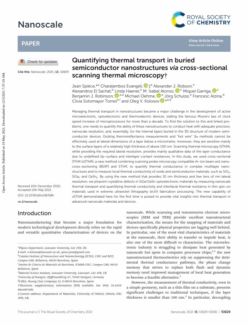
The nano-cross-sectioning (see Fig. 1a) describedelsewhere19,20 has been used to create an easily accessiblesurface section through a 3D structure for the subsurface SPManalysis of the material.17,18 Briefly, it uses three intersectingAr-ion beams aligned to a single plane that impinge on asample side at a small negative angle (∼−5°) from below thesample surface. As the beam exits at a glancing angle to thesample surface, we call this technique beam-exit nano-cross-sectional polishing.18,21 The cross-sectioned surface obtainedhas a wedge-like geometry and sub-nm surface roughness,making it fully compatible for studies via SPM methods.Equally essential, the glancing angle of the ion beam, and the
Fig. 1 (a) Schematic representation of nano-cross-sectioning beam-exit cross-section polishing (BEXP); Ar ions impinge on the sample edgeat a shallow negative angle (ca. – 5°) to its surface creating a SPM com-patible cut adjacent to the intact sample surface. (b) Schematic repre-sentation of the xSThM measurement; SThM probe scans the cross-sec-tioned area of a multilayered material (The sample is presented in thenext section). The 3D topography is overlaid with the SThM response.Image dimensions: 5 × 5 × 0.77 μm.
inert nature of Ar results in negligible surface damage andpractically no modification of the measured physical pro-perties of the studied materials.
The cross-sectioned area was then thermally imaged viaSThM (see Fig. 1b). Here, SThM measurements were per-formed in an ambient environment using a commercialSPM (Bruker MultiMode Nanoscope IIIa controller) andcustom-built electronics. Acting as both a sensor and a heater,the SThM probe (Kelvin Nanotechnology, KNT-SThM-01a, 0.3N m−1 spring constant, <100 nm tip radius) is based on a SiNcantilever with gold legs connecting to a Pd film evaporated onthe tip.22 The SThM probe is one of the Wheatstonebridge resistors, thus allowing a precise monitoring of theprobe resistance as explained elsewhere.7 In this study, weused an excess temperature of 50 K with respect to the environ-ment. When scanning across the surface of the sample, theprobe is biased by a combined AC + DC voltage, and itsresistance is monitored via a modified Wheatstone bridge.23
When the SThM probe at a temperature difference ΔT abovethe sample temperature contacts the sample surface, it coolsdown depending on the heat flux q to the sample and, conse-quently, on the sample local heat transport characteristics.These temperature variations change the electricalresistance of the probe, which was quantified via calibrationtechniques described elsewhere,7,24 and used to determine thesample thermal properties. By measuring q and ΔT, the tip–sample thermal contact resistance RX = ΔT/q can be found. Toachieve this, we processed the acquired data using acalibration methodology that provides compensation for thetip geometry and ambient air conductance,25 and more impor-tantly gives comparable quantitative measurements with theones performed in a high vacuum environment (see ESI† fordetails).
Results and discussionMeasuring anisotropic thermal conductance on the nanoscale
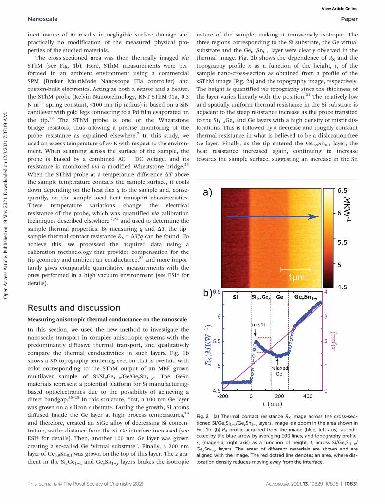
In this section, we used the new method to investigate thenanoscale transport in complex anisotropic systems with thepredominantly diffusive thermal transport, and qualitativelycompare the thermal conductivities in such layers. Fig. 1bshows a 3D topography rendering section that is overlaid withcolor corresponding to the SThM output of an MBE grownmultilayer sample of Si/SixGe1−x/Ge/GeySn1−y. The GeSnmaterials represent a potential platform for Si manufacturing-based optoelectronics due to the possibility of achieving adirect bandgap.26–28 In this structure, first, a 100 nm Ge layerwas grown on a silicon substrate. During the growth, Si atomsdiffused inside the Ge layer at high process temperatures,29
and therefore, created an SiGe alloy of decreasing Si concen-tration, as the distance from the Si–Ge interface increased (seeESI† for details). Then, another 100 nm Ge layer was growncreating a so-called Ge “virtual substrate”. Finally, a 200 nmlayer of Ge0.9Sn0.1 was grown on the top of this layer. The z-gra-dient in the SixGe1−x and GeySn1−y layers brakes the isotropic
nature of the sample, making it transversely isotropic. Thethree regions corresponding to the Si substrate, the Ge virtualsubstrate and the Ge0.9Sn0.1 layer were clearly observed in thethermal image. Fig. 2b shows the dependence of RX and thetopography profile x as a function of the height, t, of thesample nano-cross-section as obtained from a profile of thexSThM image (Fig. 2a) and the topography image, respectively.The height is quantified via topography since the thickness ofthe layer varies linearly with the position.21 The relatively lowand spatially uniform thermal resistance in the Si substrate isadjacent to the steep resistance increase as the probe transitedto the Si1−xGex and Ge layers with a high density of misfit dis-locations. This is followed by a decrease and roughly constantthermal resistance in what is believed to be a dislocation-freeGe layer. Finally, as the tip entered the Ge0.9Sn0.1 layer, theheat resistance increased again, continuing to increasetowards the sample surface, suggesting an increase in the Sn
Fig. 2 (a) Thermal contact resistance RX image across the cross-sec-tioned Si/GexSi1−x/GeySn1−y layers. Image is a zoom in the area shown inFig. 1b. (b) RX profile acquired from the image (blue, left axis), as indi-cated by the blue arrow by averaging 100 lines, and topography profile,x, (magenta, right axis) as a function of height, t, across Si/GexSi1−x/GeySn1−y layers. The areas of different materials are shown and arealigned with the image. The red dotted line denotes an area, where dis-location density reduces moving away from the interface.
concentration. We excluded the possibility that the thermal re-sistance variations had their origin at tip–sample contact areavariations since we did not observe any significant topographyvariations in the cross-sectioned area (see ESI note 7† for rele-vant profiles).
The most remarkable observation is that the resistance inthe GexSi1−x decreased in the middle region (red dotted area inFig. 2), which is consistent with the thermal conductivityincrease of GexSi1−x with the decrease in the Si content.30 Thissignificant continuing drop in the thermal resistance extend-ing to 200 nm thickness can be linked with the reduction ofthe dislocation density as one moves away from the interface.According to second ion mass spectroscopy (SIMS) measure-ments (see ESI note 6†), the Ge content of the GexSi1−x layerquickly increased from 0 to 80% in the first ∼25 nm. Thisregion corresponds to the sharp increase measured in thethermal resistance. Beyond the low thermal conductivity ofGexSi1−x alloys with more than 10% Ge (compared to the puresilicon one),30 such drastic changes in the layer compositionwere also likely to induce phonon scattering processes, andcreated a low thermal conductivity, which translated into ahigh thermal resistance increase. Then, between 25 and125 nm, the Ge content increased slowly from 80% to 90% inthe remaining of the layer, where the thermal resistancedecrease is observed. The thermal conductivity of the GexSi1−xalloys increases with the Ge content above 80% Ge. We canthen attribute the thermal resistance decrease to this increas-ing thermal conductivity with thickness. In the Ge only layer,our measurement affords an even lower resistance. This canalso be linked to the Ge content, which reaches 100% in thisregion (see ESI note 6†), and thus provides a higher thermalconductivity.
We then investigated two SiGex/GeSny samples that havesimilar composition, but different processing conditions,which are known to change the metastable GeSn alloy26–28
composition and crystallinity upon annealing at high tempera-tures.31 Sn mobility inside the Ge can also increase drasticallywith temperature with Sn atoms tending to form clusters andsegregates.28 To assess these effects, we compared twosamples: an as grown sample, and a sample that was sub-sequently annealed at 500 °C prior to the xSThM characteriz-ation. Fig. 3 shows the thermal resistance for these twosamples. For comparison purposes, we normalized the signalsto both the Si and Ge layers, which should not change due tothe annealing process. Here, we observed almost no differencein the thermal transport in the Si1−xGex region between the as-grown and annealed sample, which would be expected, as theannealing temperatures were well below ones needed toanneal the SiGe structures. In the pure Ge region, we obtainedan almost flat response, which indicated that the spreading re-sistance was not affected by the increase of Ge layer thickness.When entering to the Ge0.9Sn0.1 layer, the resistance increasedfor both samples. This could be expected due to the lowerthermal conductivity of GeSn alloys32,33 (between 1 and 10 Wm−1 K−1) compared to pure Ge (∼20 W m−1 K−1 for 100 nmfilm32,34). However, a notable difference was observed between
the as-grown and the annealed samples by the analysis of theabsolute value and the derivative of the thermal resistance inthese layers. The lower absolute value suggests a higher con-centration of Ge near the interface. Simultaneously, the higherderivative for the annealed sample suggests, similarly to theSi1−xGex region, a different GeSn crystal quality. Annealing islikely to create clusters of Sn inside the Ge, which acted asphonon scattering elements, hence reducing the thermalconductivity.
For this complex nanostructure, xSThM here allowed forthe first time to directly link the variation of the local thermalconductance due to the layer composition, crystalline defectsand the precipitate nanostructuring, via the physical propertiesof buried layers, which would be impossible to access other-wise. The next section addresses the vital question of how touse xSThM for the quantitative thermal measurements in suchlayers.
Quantitative measurements of thermal conductivity andinterfacial thermal resistance
Having established the high performance of thermal transportmapping in 3D layers, we first used xSThM to quantitativelydeduce the thermal properties of relatively simple 3D struc-tures comprised of isotropic layers. The wedge-like cut enablesSThM measurements as function of material thickness thatchanges depending on the position of the probe across the cut(see Fig. 4a). As the tip–surface and wedge sample – substratethermal resistance are independent of the tip position, using
Fig. 3 Thermal resistance (normalized with Si and Ge layer thermal re-sistance) profile as obtained by averaging 100 lines as a function ofheight for the as-grown and annealed samples. With dotted lines, thefitted curves of the GeySn1−y region are indicated. For the as-grownsample, the slope is dy/dx ≈ 5.8 ± 0.2 × 10⁻⁴ nm−1, and for the annealed,it is dy/dx ≈ 6.9 ± 0.2 × 10⁻⁴ nm−1.
samples of varied thicknesses therefore allowed to separate thecontribution of the interfacial thermal resistance and samplethermal conductivity in order to deduce the quantitativeproperties.35–39
For the quantification of the thermal properties, weexpressed RX as a sum of two main components connected inseries: the total contact thermal resistance between the probe
and the sample, Rc, and the total thermal spreading resistancewithin the sample, Rs,
RX ¼ Rc þ Rs ð1Þ
In vacuum, Rc includes solid–solid contact thermal resis-tance, and in ambient environment, also water meniscus con-ductance.40 For the quantitative evaluation of the samplethermal resistance, we treated Rc as an effective probe-sampleinterface resistance dependent on the contact area and thesample thermophysical properties, and independent of Rs. TheSThM tip – sample contact area can be approximated7 by adisk of radius a, reflecting the solid–solid contact dimensions,and when in ambient conditions, may increase due to effectsof water meniscus, providing an effective radius of the thermalcontact.
The thermal spreading resistance depends on the nano-scale structure and the material composition of the sample. Inthe simple case of a bulk isotropic material and a contactradius above the phonon mean free path Λ, the thermalspreading resistance is given by:
Rs ¼ 14ka
; ð2Þ
where k is the thermal conductivity of the bulk material. Incase of the contact radius is much smaller than mean freepath, the ballistic approximation can be used.41 Diffusivetransport assumption remains valid if the heat source dimen-sion α is bigger than Λ, indicating that the system Knudsennumber (Kn = Λ/a) is smaller than 1. In our system, Λ wasgreatly reduced compared to the bulk values due to interfacescattering and impurities.30 Except for dislocation-free Si,where Λ ∼ 300 nm,42 Λ values are usually smaller than 50 nm,the typical effective contact radius.32 In either case, if thecontact dimensions or material did not change, the thermal re-sistance remained constant.
The basic element of any 3D nanostructure is a layer withthermal conductivity k1 on the uniform substrate with thermalconductivity, ks. The angle wedge cut through the layer and thesubstrate, produced by BEXP nano-cross-sectioning, allowed usto approximate each measurement point as a layer of variablethickness. We then could use an isotropic model for Rs for theheat spreading within the layer on a substrate as describedelsewhere:43,44
RsðtÞ ¼ 1πkla
ð10
1þ K exp � 2ξteffa
� �
1� K exp � 2ξteffa
� �2664
3775J1ðξÞ sinðξÞdξξ2 ; ð3Þ
where teff = t + rint × k1 is the effective thickness that dependson the interfacial resistance between the layer and the sub-strate per unit area, rint, and the layer thickness, t, J1 is the firstBessel function of the first kind, ξ is an integration factor andwhere K is defined as K = (1 − ks/k1)/(1 + ks/k1). Note that thismodel can be extended to the orthotropic system45 to describethermally anisotropic materials. This thickness varying
Fig. 4 (a) Schematic view of the xSThM scanning along the polishedsample with an increase in the thickness. The arrows show the heat flowdirection, with their width denoting the increased heat flow. At the limitof a thick layer, heat flow is mostly lateral within the layer. The topsurface was removed from the image because it is not nano-sectioned,its roughness is very different from the top surface one, and also the topsurface can be contaminated during the sectioning due to re-depositionof material, and these measurements should not be compared directlywith the cross-sectioned area in this case (see ESI Note 8† for thethermal image including the top surface). (b) Thermal contact resistance,RX, map of the 300 nm SiO2 on Si cross-sectioned sample. (c) RX profileacquired from the xSThM image by averaging 100 lines as a functionof height across Si/SiO2 layers in the direction shown by the bluearrow at (b).
thermal spreading resistance is connected with the variationin the direction of heat flow as layer thickness crosses from t≪ a to t ≫ a, as schematically represented in Fig. 4a. At thelimit of a thick layer with t ≫ a, the spreading resistance isdescribed by eqn (2).
We investigated three films of standard materials currentlywidely used in the semiconductor industry46,47 with potentialfor the next generation extreme UV (eUV) lithography: 60 nmspin-on carbon, 10 nm spin-on glass, complemented by the300 nm thermally grown SiO2 on a Si substrate. In a BEXPsection, thickness of the layer linearly varied with the position,and could be precisely quantified via topography.21 Most sig-nificantly, owing to the perfect near-atomic flatness of the cut,the tip–sample thermal resistance as well as the layer-substrateinterfacial thermal resistance were constant, and did notdepend on the layer thickness. This allowed us to performdirect fitting of the RX vs. t dependence using eqn (3), andtherefore independently determine k1 and rint.
As expected, Fig. 4b shows the xSThM RX map of a 300 nmthermal oxide on Si with thermal resistance of Si area lowerthan that of SiO2.
48 In Fig. 4c, topography and thermal resis-tance profiles taken along the blue arrow in Fig. 4b are shown.The thermal resistance of Si is almost stable, while for SiO2,we observed a clear increase with an increase in the thicknesscorresponding to an increasing spreading resistance. A narrowdip at the Si–SiO2 interface is attributed to the topographicalvariations at the interface that locally changes the contact areabetween the tip apex and the surface. These can occur at thejunctions of the very dissimilar materials, but are not presentas we can see in the uniform or smooth gradient materials.These topographical changes can be readily observed andeliminated from the measurements, or compensated byspecial algorithms.49 Note that the difference of Si thermal re-sistance with the sample presented in Fig. 2 is due to thedifferent tip apex radii of the probe used. When the probe wassolely in contact with the oxide layer, we can assume that thetotal tip–surface contact resistance Rc of eqn (1) is constant asmaterial and contact area were not varied. We then applied theanalytical model of eqn (3) using unknown parameters Rc, a,k1 and rint as fitting parameters (see Table 1 for the fittingresults). In order to further reduce the number of fitting para-meters, and thus increase the accuracy of the fit, we can ana-lytically remove the Rc contribution by defining a new fittingfunction f (t − t0) = Rs(t ) − Rs(t0). However, Rc could be obtained
afterwards by simply finding the offset to match the measuredresistance (see ESI† for more details). The independent deter-mination of several independent thermal parameters in asingle experiment became possible, as the measurements wereperformed for the varied thickness of the sample, which wasequivalent to the multiple experiments on the same system.39
This approach is effective if we assume that the layer thicknessdoes not affect its thermal conductivity, and that layer thermalconductivity is isotropic (see ESI† for more details).
In addition, we could use the 300 nm oxide sample as aproxy to an “infinitely thick” calibration sample, allowing todetermine the contact radius a. By assuming literature valuesfor the SiO2 thermal conductivity (kSiO2 ≈ 1 W m−1 K−1)50,51
and the interfacial thermal resistance between silicon oxideand silicon (rintSi�SiO2
� 1� 10�9Km2 W�1),50,52 this value onlyweakly affects the fitting result given the large thickness of thecalibration layer) the only fitting parameter was a. We obtaineda = 56 nm, which is reasonable for the SThM probe used, witha good fit quality (see Fig. 4b). It should be noted that all threesamples were thermally imaged sequentially under same geo-metrical settings and the same SThM probe, and therefore, nosignificant change in a was expected from sample to sample.
As eqn (3) is valid for all values of layer thickness, thepower of our method also relies on its ability to measure verythin layers. By effectively expanding the thickness scale by 5times, and hence the thickness resolution, it allowed us tostudy the physical properties of nanoscale layers that were onlyfew nm thick. Such thin layers were impossible to beaddressed by vertical cross-section due to the SThM tip dia-meter.21 Applying the same method, and using the calibratedeffective contact radius, we measured thermal conductivitiesand the interfacial resistances of 60 nm spin-on carbon and10 nm spin-on glass (see Table 1). We noted that a generalagreement of a trend between the values was obtained, asspin-on carbon was expected to be more thermally conductivethan spin-on glass. Experimental data and fitted curves areavailable in the ESI (Note 4†).
Finally, it was also possible to quantify thermal conduc-tance anisotropy of more complicated gradient structures withthe use of FEA. In this context, we studied the SixGe1−x gradi-ent material, a good candidate for high temperature thermo-electrics. We found that as the SThM probe scanned acrossdifferent layers of increased Ge concentration, the thermal re-sistance at the tip apex increased in good agreement with pre-vious studies on Si1−xGex alloys.30 Modelling the SixGe1−x byFEA enabled us to reproduce experimentally acquired thermalresistance as a function of the Ge concentration (see ESISupporting Note 2† for details).
Conclusions
Combining an SPM-compatible nano-cross-sectional tool withSThM, we were able to map and measure with nanoscaleresolution the thermal conductivity and interfacial thermal re-sistance of buried layers and interfaces in complex gradient
Table 1 Parameters obtained by fitting eqn (1) to experimental data.For SiO2, literature values are used to obtain a and rint. Grey shaded cellsare assumed values with contact radius for the probe for spin-on carbonand spin-on glass taken from the SiOx calibration measurements
compound semiconductor nanostructures, which were notaccessible previously. We applied a new approach to the inves-tigation of the thermal conductance of nanomaterials, provid-ing the depth profiling of thermophysical properties with adepth resolution below 10 nm. We have directly measured heattransport in nano-layered anisotropic systems, such as poten-tial optoelectronic Si/SixGe1−x/Ge/GeySn1−y and thermoelectricSixGe1−x materials, showing an excellent match with thetheoretical data with no fitting parameters, and observingcomposition variations and dislocation-impeded thermaltransport in nanoscale thin layers. Furthermore, using a com-plimentary modelling approach, we could deduce the quanti-tative values of thermal conductivity in microelectronic thinfilms and molecular beam epitaxy layers for the next gene-ration optoelectronics and thermoelectrics. Our study demon-strates the ability to differentiate between thermal conductivityand interfacial thermal resistance in these samples, and toexplore local stoichiometry and crystalline defects in nano-structured materials and devices. This approach could prove tobe vitally important for quantitative nanoscale thermal charac-terization aspects that are currently largely missing innanomanufacturing.
Author contributions
O.K., J.S. and B.R. conceived the idea of the approach and itsapplication. J.S. performed the measurements, data analysisand modelling. C.E. performed the vacuum experiments. L.H.and A.R. prepared the sample with BEXP, and helped with theexperiments. L.H., M.O. and J.S. grew the SiGeSn samples, andprovided insights on the sample structure and behavior. M.A.and M.G. prepared the SiGe samples. A.S., F.A., and C.S. pro-vided the samples and interpretation of the thermal propertiesof SiGe. O.K., J.S., E.C provided interpretation of the experi-mental data and theoretical analysis. J.S. drafted the manu-script, O.K., C.E. revised it, and all authors contributed to itsfinal version.
Conflicts of interest
There are no conflicts to declare.
Acknowledgements
The authors acknowledge the EU QUANTIHEAT FP7 projectno. 604668 and the Horizon 2020 Graphene Flagship Core 3project no. 881603, EPSRC EP/G015570/1 EP/K023373/1, EP/G06556X/1. EP/V00767X/1 and EP/P006973/1 and FaradayInstitution NEXGENNA project for the overall support, andPaul Instrument Fund, c/o The Royal Society grant on“Infrared non-contact atomic force microscopy (ncAFM-IR)”for the equipment support. We are also grateful to our indus-trial collaborators Leica Microsystems, Lancaster MaterialsAnalysis Ltd and Bruker for the financial and instrumentation
support. LTD to ICN2 is supported by the Spanish MINECO(Severo Ochoa Centers of Excellence Program under GrantSEV-2017-0706 and CEX2019-000917-S) and by the Generalitatde Catalunya (Grants 2017SGR806, 2017SGR488, and theCERCA Program). We thank Severine Gomès from CNRS andHarry Hoster from Lancaster Energy for the helpful discus-sions on the measurements, and Andy Cockburn and MikeKocsic from IMEC for the interesting materials and discussionof applications.
Notes and references
1 C. A. Mack, IEEE Trans. Semicond. Manuf., 2011, 24, 202–207.
2 A. Majumdar, Nat. Nano., 2009, 4, 214–215.3 S. W. Fong, C. M. Neumann and H. P. Wong, IEEE Trans.
Electron Devices, 2017, 64, 4374–4385.4 S. Volz, Microscale and nanoscale heat transfer, Springer,
2007.5 H. J. Jang, C. R. Ryder, J. D. Wood, M. C. Hersam and
D. G. Cahill, Adv. Mater., 2017, 29, 1700650.6 W. Jeong, S. Hur, E. Meyhofer and P. Reddy, Nanoscale
Microscale Thermophys. Eng., 2015, 19, 279–302.7 S. Gomès, A. Assy and P.-O. Chapuis, Phys. Status Solidi A,
2015, 212, 477–494.8 M. E. Pumarol, M. C. Rosamond, P. Tovee, M. C. Petty,
D. A. Zeze, V. Falko and O. V. Kolosov, Nano Lett., 2012, 12,2906–2911.
9 L. Shi and A. Majumdar, J. Heat Transfer, 2002, 124, 329–337.
10 V. V. Gorbunov, N. Fuchigami, J. L. Hazel andV. V. Tsukruk, Langmuir, 1999, 15, 8340–8343.
11 K. Luo, R. W. Herrick, A. Majumdar and P. Petroff, Appl.Phys. Lett., 1997, 71, 1604–1606.
12 T. Lee, X. Guo, G. Shen, Y. Ji, G. Wang, J. Du, X. Wang,G. Gao, A. Altes and L. Balk, Microelectron. Reliab., 2002,42, 1711–1714.
13 K. W. Park, E. M. Krivoy, H. P. Nair, S. R. Bank andE. T. Yu, Nanotechnology, 2015, 26, 265701.
14 J. Juszczyk, M. Krzywiecki, R. Kruszka and J. Bodzenta,Ultramicroscopy, 2013, 135, 95–98.
15 E. Jung, G. Hwang, J. Chung, O. Kwon, J. Han, Y.-T. Moonand T.-Y. Seong, Appl. Phys. Lett., 2015, 106, 041114.
16 D. Choi, N. Poudel, S. Park, D. Akinwande, S. B. Cronin,K. Watanabe, T. Taniguchi, Z. Yao and L. Shi, ACS Appl.Mater. Interfaces, 2018, 10, 11101–11107.
17 J. L. Bosse, I. Grishin, B. D. Huey and O. V. Kolosov, Appl.Surf. Sci., 2014, 314, 151–157.
18 O. V. Kolosov, I. Grishin and R. Jones, Nanotechnology,2011, 22, 185702.
19 O. V. Kolosov and I. Grishin, US Patent 9,082,587,2015.
20 A. J. Robson, I. Grishin, R. J. Young, A. M. Sanchez,O. V. Kolosov and M. Hayne, ACS Appl. Mater. Interfaces,2013, 5, 3241–3245.
21 A. J. Robson, I. Grishin, R. J. Young, A. M. Sanchez,O. V. Kolosov and M. Hayne, ACS Appl. Mater. Interfaces,2013, 5, 3241–3245.
22 P. S. Dobson, G. Mills and J. M. R. Weaver, Rev. Sci.Instrum., 2005, 76, 054901.
23 P. Tovee, M. E. Pumarol, D. A. Zeze, K. Kjoller andO. Kolosov, J. Appl. Phys., 2012, 112, 114317.
24 C. Evangeli, J. Spiece, S. Sangtarash, A. J. Molina-Mendoza,M. Mucientes, T. Mueller, C. Lambert, H. Sadeghi andO. Kolosov, Adv. Electron. Mater., 2019, 5, 1900331.
25 J. Spiece, C. Evangeli, K. Lulla, A. Robson, B. Robinson andO. Kolosov, J. Appl. Phys., 2018, 124, 015101.
26 N. Bhargava, J. P. Gupta, N. Faleev, L. Wielunski andJ. Kolodzey, J. Electron. Mater., 2017, 46, 1620–1627.
27 W. Wang, L. Li, Q. Zhou, J. Pan, Z. Zhang, E. S. Tok andY.-C. Yeo, Appl. Surf. Sci., 2014, 321, 240–244.
28 L. Kormoš, M. Kratzer, K. Kostecki, M. Oehme, T. Šikola,E. Kasper, J. Schulze and C. Teichert, Surf. Interface Anal.,2017, 49, 297–302.
29 M. Oehme, D. Buca, K. Kostecki, S. Wirths, B. Holländer,E. Kasper and J. Schulze, J. Cryst. Growth, 2013, 384, 71–76.
30 A. Iskandar, A. Abou-Khalil, M. Kazan, W. Kassem andS. Volz, J. Appl. Phys., 2015, 117, 125102.
31 H. Mahmodi and M. R. Hashim, Mater. Res. Express, 2016,3, 106403.
32 S. N. Khatami and Z. Aksamija, Phys. Rev. Appl., 2016, 6,014015.
33 N. Uchida, T. Maeda, R. R. Lieten, S. Okajima, Y. Ohishi,R. Takase, M. Ishimaru and J.-P. Locquet, Appl. Phys. Lett.,2015, 107, 232105.
34 R. Cheaito, J. C. Duda, T. E. Beechem, K. Hattar,J. F. Ihlefeld, D. L. Medlin, M. A. Rodriguez, M. J. Campion,E. S. Piekos and P. E. Hopkins, Phys. Rev. Lett., 2012, 109,195901.
35 A. Makris, T. Haeger, R. Heiderhoff and T. Riedl, RSC Adv.,2016, 6, 94193–94199.
36 R. Heiderhoff, H. Li and T. Riedl, Microelectron. Reliab.,2013, 53, 1413–1417.
37 S. Gome, L. David, V. Lysenko, A. Descamps, T. Nychyporukand M. Raynaud, J. Phys. D Appl. Phys., 2007, 40, 6677–6683.
38 J. Juszczyk, A. Kazmierczak-Balata, P. Firek and J. Bodzenta,Ultramicroscopy, 2017, 175, 81–86.
39 J. L. Bosse, M. Timofeeva, P. D. Tovee, B. J. Robinson,B. D. Huey and O. V. Kolosov, J. Appl. Phys., 2014, 116,134904.
40 A. Assy and S. Gomes, Nanotechnology, 2015, 26, 355401.41 R. Prasher, Nano Lett., 2005, 5, 2155–2159.42 K. T. Regner, D. P. Sellan, Z. Su, C. H. Amon,
A. J. H. McGaughey and J. A. Malen, Nat. Commun., 2013, 4,1640.
43 Y. S. Muzychka, M. M. Yovanovich and J. R. Culham,J. Thermophys. Heat Transfer, 2004, 18, 45–51.
44 Y. S. Muzychka, J. Thermophys. Heat Transfer, 2014, 28, 313–319.
45 F. Menges, H. Riel, A. Stemmer, C. Dimitrakopoulos andB. Gotsmann, Phys. Rev. Lett., 2013, 111, 205901.
46 A. Frommhold, R. E. Palmer and A. P. Robinson, J. Micro/Nanolithogr., MEMS, MOEMS, 2013, 12, 033003–033003.
47 A. Frommhold, J. Manyam, R. E. Palmer andA. P. G. Robinson, Microelectron. Eng., 2012, 98, 552–555.
48 B. Deng, A. Chernatynskiy, M. Khafizov, D. H. Hurley andS. R. Phillpot, J. Appl. Phys., 2014, 115, 084910.
49 P. Klapetek, J. Martinek, P. Grolich, M. Valtr and N. J. Kaur,Int. J. Heat Mass Transfer, 2017, 108, 841–850.
50 A. Al Mohtar, G. Tessier, R. Ritasalo, M. Matvejeff,J. Stormonth-Darling, P. Dobson, P. Chapuis, S. Gomès andJ. Roger, Thin Solid Films, 2017, 642, 157–162.
51 K. Goodson, M. Flik, L. Su and D. Antoniadis, J. HeatTransfer, 1994, 116, 317–324.
52 J. Chen, G. Zhang and B. Li, J. Appl. Phys., 2012, 112,064319.