Quantitative Biaxial Texture Analysis with Reflection High-Energy Electron Diffraction for Ion Beam-Assisted Deposition of MgO and Heteroepitaxy of Perovskite Ferroelectrics Thesis by Rhett Ty Brewer In Partial Fulfillment of the Requirements For the Degree of Doctor of Philosophy California Institute of Technology Pasadena, California 2004 (Defended July 10, 2003)
Transcript
Quantitative Biaxial Texture Analysis with Reflection High-Energy Electron Diffraction for
Ion Beam-Assisted Deposition of MgO and Heteroepitaxy of Perovskite Ferroelectrics
Table of Figures Figure 1.1: The crystal structure of the ferroelectric perovskite BaTiO3. At temperatures above the Curie temperature (120o C) the crystal is cubic (a). When the crystal cools below the Curie temperature there is a tetragonal distortion (b) creating a long c-axis and two short a-axes. The c/a ratio is 1.01. The lattice distortion results in a spatial off-set between positively and negatively charged ions, causing a spontaneous electric dipole along the c-axis. 3 Figure 1.2: Actuator material figures of merit. Adopted by K. Bhattacharya from Krulevitch et al. (SMA: Shape-memory alloy, ES: Electrostatric, EM: Electromagnetic, PZT: Piezoelectric Lead-Zirconate-Titanate). 4 Figure 1.3: Schematic of a ferroelectric membrane linear actuator using stress and electrical fields. a) With zero electric field the stress orients the c-axis in plane, elongating the membrane, and causing the center of the membrane to sink. b) With the application of an electric field perpendicular to the membrane, the ferroelectric dipole moment aligns with the electric field and the shorter a-axes are aligned in-plane, shrinking the membrane and lifting the center up a distance ∆x, which is the linear translation attainable from this structure. 5 Figure 1.4: (a) Randomly oriented polycrystalline film. (b) Biaxially textured polycrystalline film. Biaxially textured films have a preferred out-of-plane orientation (side view) and a preferred in-plane orientation (top view). 7 Figure 1.5: Schematic of an ion beam-assisted deposition system. For MgO the optimal angle θ is 45o 8 Figure 1.6: Reflection high-energy electron diffraction (RHEED) schematic. High-energy electrons (15-50 keV) impinge on a crystal at grazing incidence, diffract, and are detected by taking an image of the electron pattern created on a phosphorescent screen. 10 Figure 1.7: Ewald sphere construction of electron diffraction. The incident electron wave vector is k, the scattered electron wave vector is p, and ∆k is the change in the electron wave vector, which must be equal to an inverse lattice vector. 11 Figure 2.1: Schematic representation of the variables used to create a polycrystalline scattering potential. Each grain is addressed individually and given an envelope function, Θg, which is one on the inside and zero outside the grain. Each grain is also given an orientation using Bg, which rotates the crystal axis of the grain around the x, y, and z-axis by the angle ωx, ωy, and φ, respectively. 24 Figure 2.2: Simulated MgO RHEED patterns, 25 keV at 2.6o incidence angle, as the parameters for grain size (L), effective electron penetration depth (h), and out-of-plane
xxi
orientation distribution (∆ω) are changed. Images a-c have h = 5 nm, ∆ω = 0o and a) L = 5 nm, b) L = 10 nm, and c) L = 25 nm. Images d-f have L = 10 nm, ∆ω = 0o, and d) h = 5 nm, e) h = 10 nm, and f) h = 25 nm. Images g-I have h = 5 nm, L = 10 nm, and g) ∆ω = 4o, h) ∆ω = 8o, and i) ∆ω = 12o. 26 Figure 2.3: Simulated RHEED pattern of 20 keV electrons at 1.2o grazing incidence along [100] from well-textured polycrystalline MgO with effective lateral grain size L = 4 nm, electron penetration depth h = 1 nm, out-of-plane grain orientation distribution ∆ω
= 7o, and in-plane orientation distribution ∆φ = 14o. The qualitative effects of these parameters upon the RHEED spot shapes and relative intensities are indicated. 27 Figure 2.4: Calculated horizontal MgO (044) diffraction spot width as a fraction of the distance between the (004) and (024) diffraction spots. 28 Figure 2.5: Simulated width of the (044) MgO diffraction spot in the direction perpendicular to the non-diffracted beam. The width is normalized to the distance between the (004) and (024). In a) the effective electron penetration depth (h) is set to 5 nm, while in b) the grain size (L) is set to 10 nm. 29 Figure 2.6: Schematic of a RHEED in-plane rocking curve experiment. Incident electrons k from the electron gun are diffracted by the polycrystalline film into wave vectors p, which are collected on a phosphorous screen and imaged (the RHEED pattern). The substrate is rotated about its vertical axis and the intensity of several diffraction spots are recorded as a function of the rotation angle φ. The rocking curves are characterized by the FWHM from a Gaussian fit. 30 Figure 2.7: Simulated in-plane rocking curve FWHM (∆φ degrees) for the MgO a) (024) and b) (044) diffraction spots, where the out-of-plane orientation distribution is equal to 5o FWHM (∆ω). The in-plane rocking curve displays an inverse relationship to grain size (L) for grain sizes smaller than 20 nm. 31 Figure 2.8: Simulated in-plane rocking curve FWHM (∆φ degrees) for the MgO a) (024) and b) (044) diffraction spots and grain size set to 10 nm. The in-plane rocking curve displays a direct dependence on out-of-plane orientation distribution (∆ω). 32 Figure 2.9: Comparison of the simulated RHEED dependence of MgO and BaTiO3 on biaxial texture. a) For grain size (L = 10 nm) and effective electron penetration depth (h = 6nm) the (024) diffraction spot width in the direction perpendicular to the non-diffracted spot, as a fraction of the separation between the (004) and (024) diffraction spots, is measured as a function of the out-of-plane orientation distribution (∆ω). b) The (024) in-plane rocking curve FWHM is measured as a function of the in-plane orientation distribution (∆φ) with ∆ω = 5o FWHM and L = 10 nm. 34 Figure 2.10: Experimental MgO RHEED image at 25 keV and 2.6o incidence angle. The diffraction spots shown are those which are used for RHEED-based biaxial texture
xxii
analysis. The cuts across the diffraction spots show the directions across which the computer program measures the FWHM of the diffraction spots. 35 Figure 2.11 Experimental IBAD MgO RHEED images taken at 25 keV and 2.6o incidence. a) Top view. b) Side view. The diffuse background is significant fraction of the diffraction spot intensity. 37 Figure 2.12: RHEED image of amorphous Si3N4 taken at 25 keV and 2.6o incidence angle before IBAD MgO growth. 38 Figure 2.13: Background subtracted experimental RHEED images of IBAD MgO taken at 25 keV and 2.6o incidence angle. These are the background subtract images of Figure 2.11. a) Top view. b) Side view. 39 Figure 2.14: TEM image of IBAD MgO on amorphous Si3N4. The four fold symmetric arcs indicate that the MgO has a preferred in-plane orientation and the angular width of the arcs is a measurement of the in-plane orientation distribution (∆φ). 45 Figure 2.15: In-plane and out-of-plane x-ray rocking curves of IBAD MgO (002) with in-plane orientation distribution ∆φ = 10.6o and out-of-plane orientation distribution ∆ω = 6.5o FHWM. The rocking curve was taken at APS. 46 Figure 2.16: In-plane orientation distribution (∆φ) measured by RHEED analysis versus TEM or X-ray diffraction measurements. X-ray rocking curves collected using either a rotating anode source at Los Alamos or synchrotron radiation from the advanced photon source (APS). The error bars originate from limitations in deconvoluting the effects of out-of-plane orientation distribution and grain size measurements using RHEED. 49 Figure 2.17: In-plane (∆φ) and out-of-plane (∆ω) orientation distribution for IBAD MgO growth as a function of film thickness measured using RHEED. The lines are a fit to the data. 50 Figure 2.18: RHEED intensity of two separate Si Bragg rods as amorphous MgO was deposited on the Si (001) substrate. RHEED was performed at 25 keV at 2.6o incidence angle. 51 Figure 2.19: Out-of-plane orientation distribution (∆ω) measured using RHEED and synchrotron x-ray out-of-plane rocking curves. The line is a linear fit to the data. 53 Figure 3.1: Schematic of an ion beam-assisted deposition (IBAD) apparatus. The ion source is typically a Kaufmann ion gun and the growth material is deposited using physical vapor deposition (PVD). The optimal incidence angle of the ion bombardment (θ) depends on the film, 45o is optimal for MgO33 and 55.4o is optimal for yttrium stabilized zirconia. 59
xxiii
Figure 3.2: Biaxially textured film. The side view shows the MgO grains growing out of amorphous Si3N4 with a preferred out-of-plane direction (the arrows indicate the (001) direction). On the right, the in-plane (001) planes, represented by the arrows, nominally align around the direction of the Ar+ bombardment. 60 Figure 3.3: Molecular dynamics simulation of FCC crystals after twenty 100 eV, perpendicular Ar ion impacts. The top crystal has a (110) c-axis orientation and the bottom crystal has a (111) c-axis orientation. Crystal damage depends on the crystal direction oriented toward the ion flux. 63 Figure 3.4: In-plane alignment direction for IBAD YSZ as a function of r (ion/atom flux ratio) and ion bombardment angle. The different symbols represent that the films were grown by different deposition methods, e.g., sputter deposition and e-beam evaporation, and substrate temperatures, e.g., room temperature to 600o C. 64 Figure 3.5: Cross section TEM of IBAD MgO (deposited at 300 C) in which the ion beam was incident at roughly 45 degrees with respect to the normal of the substrate and image planes. 68 Figure 3.6: In situ RHEED images from a continuous IBAD MgO growth experiment where the film thickness is equal to: 2.5 nm (a), 3.1 nm (b), 3.6 nm (c), and 4.2 nm (d). The field of view contains diffraction spots from (024) , in the upper left corner, to (046) in the lower right corner. 71 Figure 3.7: RHEED images from different IBAD MgO films grown to: 1.9 nm (a), 3.7 nm (b), 4.6 nm (c), and 4.8 nm (d). The field of view contains diffraction spots from (024) , in the upper left corner, to (046) in the lower right corner. 72 Figure 3.8: TEM dark field images and diffraction patterns for IBAD MgO films with thicknesses equal to: 1.9 nm (a) (top image), 3.7 nm (b) (second image), 4.6 nm (c) (third image), and 4.8 nm (d) (bottom image). 74 Figure 3.9: Fraction of crystalline material observed for IBAD MgO with dark field TEM as a function of film thickness. In-plane orientation distribution (∆φ) measured as a function of film thickness. 75 Figure 3.10 In-plane (∆φ) and out-of-plane (∆ω) orientation distribution for IBAD MgO growth as a function of film thickness measured using RHEED. The lines are a fit to the data. In-plane orientation distribution (∆φ) measured using grazing incidence x-ray diffraction by Groves et al. are included for comparison. 77 Figure 3.11: In situ RHEED measurements of out-of-plane orientation distribution (∆ω) as a function of film thickness for ion/MgO flux ratios from 0.37 to 0.52. 78
xxiv
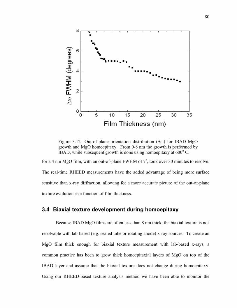
Figure 3.12: Out-of-plane orientation distribution (∆ω) for IBAD MgO growth and MgO homoepitaxy. From 0-8 nm the growth is performed by IBAD, while subsequent growth is done using homoepitaxy at 600o C. 80 Figure 3.13: Optimal in-plane (∆φ) and out-of-plane (∆ω) orientation distributions for IBAD MgO growth with 750 eV Ar+ ions as a function of ion/MgO molecule flux ratio. Measurements were performed using RHEED-based analysis and the lines are fits to the data. 82 Figure 4.1: Schematic of a ferroelectric membrane linear actuator using stress and electrical fields. a) With zero electric field the stress orients the c-axis in plane, elongating the membrane, and causing the center of the membrane to sink. b) With the application of an electric field perpendicular to the membrane, the ferroelectric dipole moment aligns with the electric field and the shorter a-axes are aligned in-plane, shrinking the membrane and lifting the center up a distance ∆x, which is the linear translation attainable from this structure. 92 Figure 4.2: A polarization hysteresis loop plots the dielectric polarization as a function of applied voltage. Points C and E are the positive and negative remnant polarizations (Pr), respectively. The coercive field (Ec) must be calculated from the voltage drop across the ferroelectric material when the net polarization goes to zero. 93 Figure 4.3: Schematic of a dynamic contact mode electrostatic force microscopy (DC-EFM) system. 95 Figure 4.4: Schematic of the IBAD MgO and oxide MBE chamber. 100 Figure 4.5: Side view of the IBAD MGO and oxide MBE chamber. 101 Figure 4.6: Front view of the IBAD MgO and oxide MBE chamber. 102 Figure 4.7: Top view of the IBAD MgO and oxide MBE chamber. 103 Figure 4.8: X-ray θ−2θ curves from PBT deposited by MOCVD and sol-gel on single-crystal MgO (001) and biaxially textured MgO. An x-ray θ−2θ curve from MBE BST is also included. 106 Figure 4.9: C/a ratio of BaxPb1-xTiO3 as a function of Ba composition (x). 108 Figure 4.10: RHEED images of PBT grown on biaxially textured MgO. Sol-gel PBT (a) and MOCVD (c) PBT RHEED images from films deposited on MgO templates made from 8 nm of IBAD MgO and an additional 20 nm of homoepitaxial MgO grown at 600o C. Sol-gel (b) and MOCVD (d) PBT RHEED images from films deposited on MgO templates made from 8 nm of IBAD MgO. 109
xxv
Figure 4.11: RHEED image of BST grown heteroepitaxially on biaxially textured MgO made from 8 nm of IBAD MgO and 20 nm of homoepitaxial MgO grown at 600o C. 110 Figure 4.12: Out-of-plane (∆ω) and in-plane (∆φ) orientation distributions of biaxially textured MgO templates and the heteroepitaxial perovskite (BST or PBT) deposited by MBE, MOCVD, or sol-gel. 112 Figure 4.13: Cross section TEM images of MOCVD PBT grown on single-crystal MgO (001). b) is a high-resolution image of one of the 45o defects in (a). 114 Figure 4.14: Diffraction patterns from MOCVD PBT grown on (a) single-crystal MgO (001) and (b) biaxially textured MgO. 115 Figure 4.15: MOCVD PBT grown on biaxially textured MgO. In some areas the MgO layer appears crystalline (a), while in other areas it does not appear to be crystalline (b). 116 Figure 4.16: a) High-resolution TEM image of the interface between biaxially textured MgO and MOCVD PBT. b) Plan view diffraction pattern of MOCVD PBT on biaxially textured MgO. 117 Figure 4.17: Cross section TEM high-resolution image of sol-gel PBT on biaxially textured MgO. b) Close up of a small interface region from image (a). 119 Figure 4.18: Cross section TEM high-resolution image of BST on biaxially textured MgO. (b) Diffraction pattern from image (a). The diffraction pattern is a super position of diffraction spots from MgO, a BST perovskite structure, and Si. 121 Figure 4.19: Dark field TEM image of the BST/ biaxially textured MgO/ amorphous Si3N4 /Si film stack. MgO grain orientation propagates into the BST layer. 122 Figure 4.20: (a) Contact AFM topographic image of sol-gel PBT deposited on biaxially textured MgO. (b) Dynamic contact mode electrostatic force microscopy image of the film in (a). (c) Polarization hysteresis loops taken with the dynamic contact mode electrostatic force microscopy system from sol-gel PBT films deposited on different substrates. The biaxially textured and broad texture PBT films are 50 nm thick and the PBT on single-crystal MgO is 150 nm thick. 126 Figure 4.21: (a) Contact mode AFM topographical image of sol-gel PBT deposited on single-crystal MgO (001). (b) DC-EFM image of the film in (a). (c) A smaller DC-EFM scan of the image in (a). Decreasing the DC-EFM scan size increases sensitivity. 128 Figure 4.22: (a) Contact mode AFM image of MOCVD PBT deposited on biaxially textured MgO. (b) DC-EFM ferroelectric domain image of the topographical iamge (a). (c) Contact mode AFM image of MOCVD PBT deposited on single-crystal MgO (001).
xxvi
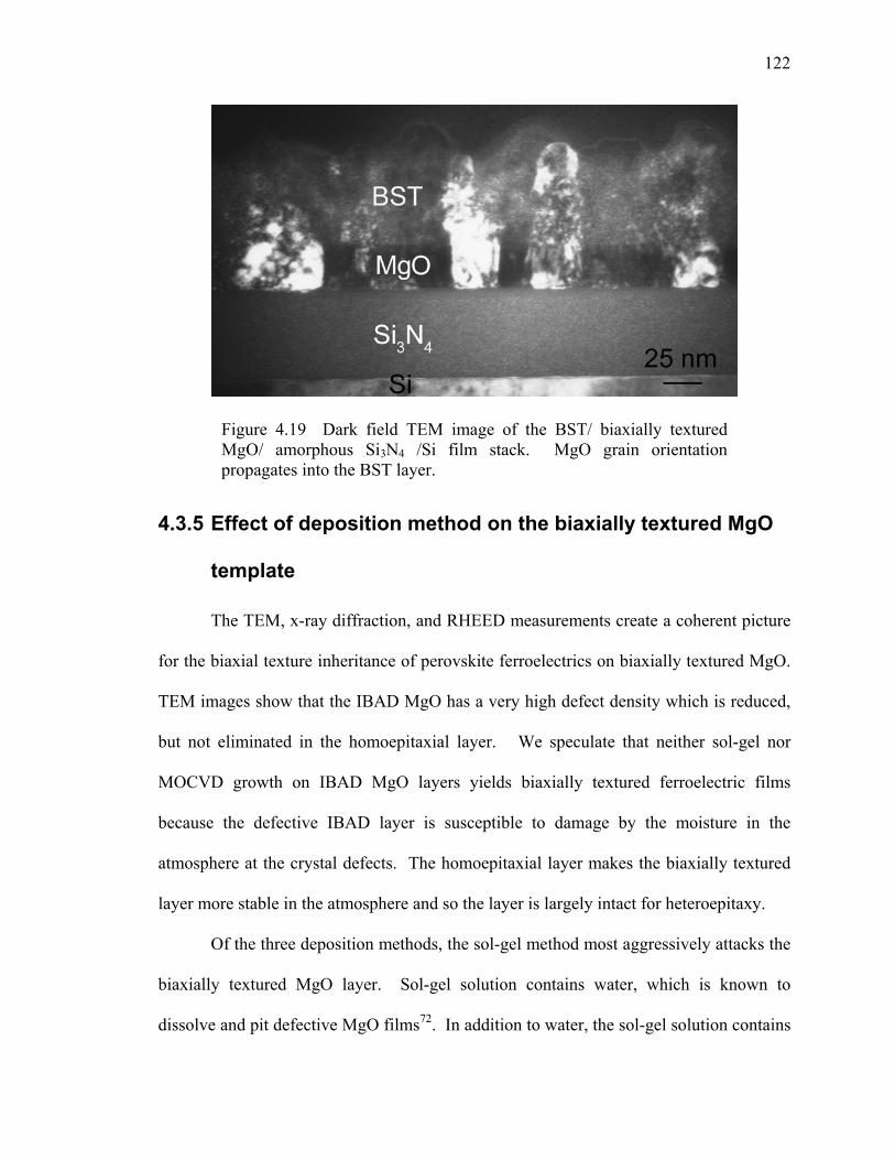
(d) DC-EFM ferroelectric domain image of the topographical image (c). (e) Polarization hysteresis loops of MOCVD deposited on different MgO substrates. 129 Figure 4.23: (a) Contact mode AFM topographical image of MBE BST deposited on biaxially texture MgO. (b) DC-EFM ferroelectric domain image of the BST in image (a). (c) Polarization hysteresis loops taken with the DC-EFM system from sol-gel and MOCVD PBT films deposited on biaxially textured MgO. A polarization hysteresis loop from MBE BST on biaxially textured MgO is also included. 131
1
Chapter 1 Introduction
Billions of dollars in semiconductor foundries and fifty years of technological
development provide enormous momentum for the continued dominance of silicon-based
electronics and systems for the foreseeable future. There is also wide-spread enthusiasm
for micro- and nano-electrical mechanical systems (MEMs and NEMs) which have the
potential to enable new technologies and create smaller, more highly integrated versions
of today’s mechanical device technologies. Silicon is also the dominant material for
MEMs device fabrication partially due to the vast technology base developed from years
of working with silicon MOS electronics and partly to facilitate MEMs integration with
silicon-based electronics.
Though preferred for processing and integration reasons, silicon is not the ideal
material for all MEMs applications. To realize miniaturized systems that can perform
multiple tasks like biochemical sensing, communications, computational processing, and
actuation requires the integration of ceramics, organics, metals, semiconductors,
ferroelectrics, and other active materials with silicon electronics. Vertical integration of
MEMs/NEMs with silicon electronics is important for device miniaturization, as well as
for device functionality. The speed would increase and the complexity would decrease
for communication between the active devices and control electronics for vertically
integrated systems compared with separate chip device solutions. Unfortunately, silicon
electronics devices are sensitive to contamination, greatly restricting the possibilities for
introducing new materials into semiconductor foundries.
The most practical integration processes will allow new materials to be used for
MEMs fabrication while still enabling the use of current silicon electronics fabrication
2
technology. One simple way to enable use of the current silicon electronics fabrication
process and introduce new materials into MEMs devices is to fabricate the active
structures during backend processing, i.e., after the silicon electronics have been
fabricated and protected from contamination. One of the main challenges with this
approach is that any subsequent processing must be performed at relatively low
temperatures (< 450o C) to preserve the integrity of the silicon devices. Another major
challenge is that the surface available for growth (metal layers and low-k dielectric
materials) is not single-crystalline and not suitable for heteroepitaxy.
1.1 Ferroelectrics and Si integration
Ferroelectric materials contain components not easily compatible with silicon-
based electronics fabrication, but could increase functionality of silicon-based
MEMs/NEMs. Ferroelectric materials exhibit a spontaneous electric dipole moment
without the application of an external electric field. Perovskite ferroelectrics produce a
spontaneous dipole moment as the result of a tetragonal crystal lattice distortion which
offsets the center of the positively charged ions from the center of the negatively charged
ions in the crystal. For example, in its paraelectric state at elevated temperatures, BaTiO3
possesses a cubic structure (Figure 1.1a). Once BaTiO3 cools below its Curie
temperature at 120o C, the unit cell experiences a tetragonal distortion along the (001)
lattice plane creating a spontaneous dipole (Figure 1.1b). The tetragonal distortion of
perovskite ferroelectrics ranges from a c/a (axis) ratio of 1.01 for BaTiO3 to 1.06 for
PbTiO3.
Krulevitch et al. identified frequency response and work/volume as important
figures of merit for MEMs actuator materials. A plot illustrating how various actuator
3
candidate materials compare is included as Figure 1.21. Theoretically, high-strain
ferroelectrics (like BaTiO3 and PbTiO3) are desirable actuator materials because they
combine high work/volume with high-frequency response.
The orientation of the tetragonal distortion can be switched by either the
application of an electric field or strain. One can imagine linear actuator structures
fabricated out of a ferroelectric membrane or bridge structure which uses a combination
of electric fields and stress to accomplish linear actuation. Linear actuation from a
stress/electric field actuator is depicted pictorially in Figure 1.3. The force applied
normal to the ferroelectric thin film could be pressure from a trapped gas or it could be
from a rod attached to the structure to be moved by the actuator. In Figure 1.3a, no
electric field is applied across the ferroelectric membrane so the tensile stress causes the
Figure 1.1 The crystal structure of the ferroelectric perovskite BaTiO3. At temperatures above the Curie temperature (120o C) the crystal is cubic (a). When the crystal cools below the Curie temperature there is a tetragonal distortion (b) creating a long c-axis and two short a-axes. The c/a ratio is 1.01. The lattice distortion results in a spatial off-set between positively and negatively charged ions, causing a spontaneous electric dipole along the c-axis.
4
c-axes to rotate into the plane of the film. As a result the overall membrane lateral length
is elongated and the center of the membrane depresses. In Figure 1.3b, an electric field is
applied perpendicular to the membrane, inducing the electric dipoles to orient along the
direction of the applied electric field. If the electric field imposed across the thin plane of
the film exceeds a minimum coercive field, then the electric dipole, and therefore the c-
axis, is forced to orient in the direction of the electric field, despite the tensile stress
which tends to orient the c-axis in the plane of the ferroelectric membrane. If all crystals
have their c-axes oriented out-of-plane, the shorter a-axes are oriented in the plane of the
ferroelectric membrane, making the ferroelectric membrane as short and flat as possible,
lifting the center of the membrane. Releasing the electric field would allow the
membrane to revert to the state shown in Figure 1.3a. The translation distance for this
Figure 1.2 Actuator material figures of merit. Adopted by K. Bhattacharya from Krulevitch et al.1 (SMA: Shape-memory alloy, ES: Electrostatric, EM: Electromagnetic, PZT: Piezoelectric Lead-Zirconate-Titanate).
5
linear actuator structure, ∆x in Figure 1.3, is proportional to the length of the membrane
and the c/a ratio. This type of actuator could either exploit the changing size of the cavity
beneath the membrane to form a micropump or exploit the vertical displacement of the
rod by attaching it to a mirror for optical switching.
There has been considerable success in efforts to grow high-quality single-
crystalline perovskites on silicon. Molecular beam epitaxy (MBE) was used to grow
SrTiO3 on (001) Si with “perfect registry”2. While essentially defect free perovskite
ferroelectrics can be grown epitaxially on Si, for use as high K gate dielectrics, this does
Figure 1.3 Schematic of a ferroelectric membrane linear actuator using stress and electrical fields. a) With zero electric field the stress orients the c-axis in plane, elongating the membrane, and causing the center of the membrane to sink. b) With the application of an electric field perpendicular to the membrane, the ferroelectric dipole moment aligns with the electric field and the shorter a-axes are aligned in-plane, shrinking the membrane and lifting the center up a distance ∆x, which is the linear translation attainable from this structure.
6
not solve the silicon/ferroelectric-based MEMs integration problem. Once the integrated
circuits are fabricated, the Si (001) surface is not accessible for heteroepitaxy. With
layers of oxides, metallization, and low-k dielectrics, any candidate techniques for
building actuators on top of transistors must start with an amorphous layer.
Wafer bonding is a promising technique that could integrate single-crystal
ferroelectrics with amorphous layers. Wafer bonding is accomplished by pressing a
ferroelectric single-crystal wafer against a flat amorphous surface (Si, SiO2, Si3N4),
which could be used to cap the silicon integrated circuits. If the surfaces are sufficiently
smooth and contaminate free, the Van der Waals forces will bring the surfaces into
atomic contact. A high-temperature annealing step changes these bonds to covalent
bonds, resulting in single-crystalline films on amorphous substrates. Unfortunately, this
simplistic explanation of the wafer bonding process masks the technological difficulties
of this technique. Surface contamination is often a barrier to successful wafer bonding.
Excessive stress caused by coefficient of thermal expansion mismatches can also
introduce difficulties. Finally, the desired ferroelectric layer thickness is much thinner
than an entire wafer. Polishing a layer to the correct thickness is impractical, but layer
transfer methods like crystal ion slicing3 or some version of the Smart Cut process4
provide hope for this alternative in the future.
Another route for ferroelectric/silicon integration is to create biaxially textured
ferroelectrics using a buffer layer as a heteroepitaxial template. As previously stated, the
only substrate reliably available during back end silicon processing for ferroelectric
deposition will be amorphous; however, biaxially textured films can by grown on
amorphous layers using ion beam-assisted deposition.
7
1.1.1 Ion beam-assisted deposition
In 1985, Yu et al. were the first to demonstrate that niobium thin films with
preferred in-plane and out-of-plane crystal axis orientations, i.e., biaxially textured (see
Figure 1.4), could be grown on amorphous substrates using ion beam-assisted deposition
(IBAD)5. A standard IBAD system schematic is included as Figure 1.5. IBAD consists
of physical vapor deposition on an amorphous substrate with simultaneous ion
bombardment of the substrate (ion bombardment energy is on the order of 1 keV).
Wang et al. recently showed that IBAD could be used to create highly aligned,
biaxially textured MgO on amorphous Si3N4. The in-plane orientation distribution full
width at half maximum (FWHM) was < 7o and the out-of-plane orientation distribution
FHWM was < 4o 6. MgO is a well-known heteroepitaxial template for ferroelectrics like
BaTiO37 and PbTiO3
8. Therefore, it is expected that biaxially textured ferroelectrics on
ultimately amorphous substrates can be constructed by using IBAD MgO as a template.
Figure 1.4 (a) Randomly oriented polycrystalline film. (b) Biaxially textured polycrystalline film. Biaxially textured films have a preferred out-of-plane orientation (side view) and a preferred in-plane orientation (top view).
8
1.1.2 Biaxially textured ferroelectrics
The literature is silent on the properties of biaxially textured ferroelectric thin
films, even though theoretically their properties should approach those of a single-
crystalline film. Biaxial texture is important for polycrystalline actuator performance
because the film elongation is directed and switchable only along the (001) crystal planes.
A randomly oriented polycrystalline film performs less than half of the actuation that a
single-crystal film produces, while a biaxially textured ferroelectric film (with the
previously mentioned out-of-plane and in-plane orientation distributions of 3o FWHM
and 7o FWHM, respectively, for MgO) can produce over 90% of the single-crystal
actuation.
Biaxial texture can also be expected to play an important role in ferroelectric
domain structure and ferroelectric domain boundary migration kinetics. Ferroelectric
materials exhibit ferroelectric domain structure and domain switching similar to those
observed in ferromagnetic materials. However, the ferroelectric dipole moments are tied
Figure 1.5 Schematic of an ion beam-assisted deposition system. For MgO the optimal angle θ is 45o6.
9
to the crystallographic directions. Randomly oriented polycrystalline films will have
neighboring grains with very different orientations, forcing the crystal grain boundaries to
be ferroelectric domain boundaries as well. A highly aligned biaxially textured
ferroelectric will have neighboring grains with only slight misalignment between the
crystallographic orientations. Subsequently, neighboring grains may have very similar
ferroelectric dipole orientations, potentially enabling ferroelectric domain boundaries to
span several grains. The energetic interaction between the well-aligned grains will be
very different from the randomly oriented neighbors. This difference should be
especially important when a field or stress is applied in an effort to reorient the
ferroelectric domains. Grain boundaries have been implicated in domain wall motion
pinning on the grounds that trapped charge at the domain boundaries inhibits domain wall
motion9. High-angle grain boundaries offer greater disruption in the crystal potential
than do low-angle grain boundaries, as attested by the ability of electrons to superconduct
across low-angle grain boundaries in YBa2C3O7-x but not in randomly oriented
polycrystalline films10. Therefore, it is reasonable to expect that ferroelectric domain
walls should migrate more easily across low-angle grain boundaries than across high-
angle grain boundaries. Experiments and theoretical computations comparing domain
switching speeds as a function of biaxial texture could yield insight into ferroelectric
domain switching across grain boundaries and crystal defects. While still untested,
biaxially textured ferroelectrics have the potential to perform like single-crystal films
with the added advantage of facile integration with silicon electronics.
10
1.2 Reflection high-energy electron diffraction (RHEED)
The performance of biaxially textured ferroelectric MEMs is likely to depend on
the biaxial texture inherited from the MgO substrate. Previous efforts to optimize the
biaxial texture of IBAD MgO have been impeded by the ex situ nature of conventional
biaxial texture analysis techniques (transmission electron microscopy (TEM) or x-ray
diffraction). Because the biaxial texture develops within 11 nm of growth, x-ray
diffraction cannot resolve biaxial texture unless the x-ray source has synchrotron
brightness. For these same reasons, the IBAD biaxial texturing mechanisms are difficult
to investigate. To circumvent these obstacles we have developed a reflection high-energy
electron diffraction (RHEED) based method for quantitative in situ biaxial texture
analysis of MgO.
A schematic of a RHEED system is included as Figure 1.6. A high-energy
electron beam (15 – 50 keV) is incident on the sample at a grazing angle (1o to 5o).
Electrons interact with the crystal potential and diffract into directions where the change
Figure 1.6 Reflection high-energy electron diffraction (RHEED) schematic. High-energy electrons (15-50 keV) impinge on a crystal at grazing incidence, diffract, and are detected by taking an image of the electron pattern created on a phosphorescent screen.
11
in the electron wave vector (∆k) is equal to an inverse lattice vector. This is the Laue
condition. This process is demonstrated using the Ewald Sphere construction, illustrated
in Figure 1.7. The incident electron wave vector is represented as k, while all elastic
scattering conditions are represented by a sphere (the intersection of the sphere with the
page is drawn as a circle) centered on the origin of the k vector. The head of the electron
wave vector points to an inverse lattice position, which is also a point on the surface of
the Ewald sphere. Where the Ewald sphere intersects inverse lattice positions a strong
diffraction condition is created because the electrons can elastically scatter by exchanging
energy with crystal phonons. The scattering vectors (∆k) are thus demonstrated to be
equal to inverse lattice vectors. The radius of the Ewald sphere for high-energy electrons
is large enough that it can be approximated as a flat sheet near the head of the incident
electron wave vector k. Because the Ewald sphere is so flat (the radius at 25 keV is
82.02 Å-1), it intersects with many inverse lattice positions and RHEED makes a 2-D
image of the inverse lattice, much like for transmission electron microscopy (TEM). The
Figure1.7 Ewald sphere construction of electron diffraction. The incident electron wave vector is k, the scattered electron wave vector is p, and ∆k is the change in the electron wave vector, which must be equal to an inverse lattice vector.
12
RHEED pattern is obtained by collecting the diffracted electrons on a phosphorous screen
and taking an image of the electron induced fluorescence.
RHEED is an ideal tool for measuring biaxial texture. Because it is an in situ
measurement technique, biaxial texture can be measured during film growth. The strong
coupling of electrons with the crystal lattice potential makes RHEED sensitive to films a
few nanometers thick. Our experiments indicate that 90% of the diffracted intensity from
25 keV electrons at 2.6o incidence angle in MgO originates in the top 1 nm of film. By
contrast, the weak interaction between x-rays and the crystal potential allows x-rays to
penetrate into microns of film, making x-ray measurements reflective of bulk film
properties. The weak interaction of x-rays with low Z (MgO) thin films is especially
problematic for measuring biaxial texture which requires high-angles of incidence for
out-of-plane orientation distribution measurements. Out-of-plane orientation
distributions cannot be measured unless the x-ray source has synchrotron brightness.
Even with a synchrotron, recording out-of-plane orientation distributions in <10 nm thick
MgO films requires a half an hour. The speed (less than one second to collect a RHEED
image), sensitivity (~1 nm of MgO), and in situ nature of RHEED experiments make it a
powerful tool for biaxial texture measurement.
1.3 Thesis outline
Of the many possible routes for ferroelectric-based MEMs/NEMs integration with
Si integrated circuits we have chosen to develop ion beam-assisted deposition as a
heteroepitaxial template for biaxially textured ferroelectrics. This approach offers a
specific set of challenges and advantages compared to other methods. The greatest
advantage originates from the fabrication flexibility resulting from the ability to create
13
biaxially textured ferroelectrics on amorphous substrates. Before fabrication of
MEMs/NEMs on a chip, the Si integrated circuits can be sealed off with diffusion barrier
layers and protected from incompatible materials associated with ferroelectric deposition.
Also, an amorphous layer can be deposited on any sacrificial or etch stop layer required
for MEMs/NEMs structural fabrication. Because this fabrication would take place after
Si integrated circuit fabrication, no new materials would need to be introduced into Si
fabrication facilities, making this approach instantly compatible with current technology.
The outline of this thesis follows the development of our capability to grow
highly aligned, biaxially textured perovskite ferroelectrics on amorphous substrates.
1.3.1 RHEED-based biaxial texture measurements
Chapter 2 details the development of RHEED as an in situ biaxial texture
measurement technique. Using a kinematical electron scattering model, we show that the
RHEED pattern from a biaxially textured polycrystalline film can be calculated from an
analytic solution to the electron scattering probability. We found that diffraction spot
shapes are sensitive to out-of-plane orientation distributions, but not to in-plane
orientation distributions, requiring the use of in-plane RHEED rocking curves to fully
experimentally determine biaxial texture. Using information from the simulation, a
RHEED-based experimental technique was developed for in situ measurement of MgO
biaxial texture. The accuracy of this technique was confirmed by comparing RHEED
measurements of in-plane and out-of-plane orientation distribution with synchrotron x-
ray rocking curve measurements. An offset between the RHEED-based and x-ray
measurements (the RHEED measured slightly narrower orientation distributions than x-
ray analysis), coupled with evidence that the biaxial texture narrows during ion beam-
14
assisted deposition, indicates that RHEED-based measurements are more appropriate for
probing surface biaxial texture than x-ray measurements.
RHEED-based biaxial texture measurement was essential to our efforts to produce
biaxially textured ferroelectrics. Biaxially textured MgO has been used as a
heteroepitaxial template for other perovskites, so optimization of the MgO biaxial texture
is essential to optimizing the biaxial texture of ferroelectrics. RHEED measurements
allow for fast optimization of MgO biaxial texture, fast analysis of MgO biaxial texture to
determine if it is suitable for ferroelectric heteroepitaxy, and fast measurement of
ferroelectric biaxial texture.
1.3.2 Biaxial texture development in IBAD MgO
Our efforts to understand biaxial texture formation in ion beam-assisted
deposition of MgO are discussed in Chapter 3. We discovered that biaxial textured MgO
emerges after about 3 nm of growth. TEM and RHEED measurements were used to
discover the initial deposition of an amorphous MgO layer, followed by an ion
bombardment-mediated solid phase crystallization of a biaxially textured film. RHEED
measurements were also used to show that once the biaxial textured film crystallized, the
out-of-plane and in-plane orientation distributions narrowed as the film thickness
increases. Finally, we optimized the IBAD MgO biaxial texture by measuring the biaxial
texture for 750 eV Ar+ ion bombardment as a function of the ion/MgO flux ratio. The
most interesting result is that the in-plane orientation distribution is limited by the out-of-
plane orientation distribution. Our experiments suggest that the minimum in-plane
orientation distribution attainable by ion beam-assisted deposition is 2o FWHM and can
15
only be achieved if the (001) MgO planes are perfectly aligned perpendicular to the
substrate (i.e., the out-of-plane orientation distribution goes to 0o FWHM).
Understanding the biaxial texture development of IBAD MgO is essential to
optimizing and controlling it for ferroelectric heteroepitaxy. The quality of the IBAD
MgO template greatly influences the ferroelectric film microstructure.
1.3.3 Biaxially textured ferroelectric films
In Chapter 4 we investigate the growth of perovskite ferroelectrics on biaxially
textured MgO templates. Sol-gel and metallorganic chemical vapor deposition
(MOCVD) were used to grow BaxPb1-xTiO3 (PBT) and molecular beam epitaxy (MBE)
was used to grow Ba0.67Sr.03Ti1.3O3 (BST). PBT grown directly on IBAD MgO surfaces
was not biaxially textured, whereas if the IBAD MgO layer was capped with an
additional 25 nm of homoepitaxial MgO before heteroepitaxy, the PBT would inherit the
biaxial texture from the MgO template. Through RHEED-based biaxial texture analysis
we observed that the in-plane orientation distribution of PBT, deposited using ex situ
techniques (not performed in the same high vacuum growth environment where the MgO
was deposited), narrowed significantly with respect to the in-plane orientation
distribution of its MgO template (from 11o to 6o FWHM). We also observed that the in-
plane orientation distribution of in situ MBE BST on biaxially textured MgO resulted in a
BST film whose in-plane orientation distribution was within 1o FWHM of the MgO
template in-plane orientation distribution. Cross section transmission electron
microscopy (TEM) was used to investigate the microstructure of the heteroepitaxial
ferroelectric films. Films deposited on biaxially textured MgO using ex situ growth
techniques (sol-gel and MOCVD) were found to have degraded MgO templates.
16
We speculate that moisture from the atmosphere degrades the MgO template by
attacking the defects in the biaxially textured MgO substrate. PBT grown on IBAD MgO
surfaces was not biaxially textured because the high defect density made the entire MgO
template subject to hydroxylation and degradation from atmospheric moisture. By
capping IBAD MgO with an MgO homoepitaxial layer, grown at 600o C, the MgO defect
density was reduced and produced biaxially textured PBT on MgO using sol-gel
synthesis and MOCVD. We also infer that PBT in-plane orientation distributions were
narrower than the MgO template because misaligned MgO grains were more highly
damaged during IBAD growth and were not fully healed by MgO homoepitaxy. These
highly damaged, misaligned grains are preferentially degraded by atmospheric moisture,
allowing PBT to preferentially nucleate on well-aligned MgO grains and to possess a
narrower in-plane orientation distribution than the MgO template by over growing less
well oriented MgO regions. The MBE BST more closely reflected the MgO template in-
plane orientation distribution because the in situ BST growth did not subject the MgO to
hydroxylation from the atmosphere, leaving all MgO grains crystalline and available for
BST nucleation.
The ferroelectric domain structure of biaxially textured PBT (grown by sol-gel
and MOCVD) and BST (grown by MBE) was mapped using dynamic contact mode
electrostatic force microscopy (DC-EFM). C-axis domains were observed to be
associated with large grains. Polarization hysteresis loops obtained with the DC-EFM at
several locations on each film indicate that the entire film is ferroelectric on the scale of
the AFM tip size.
17
1 P. Krelevitch, A. P. Lee, P. B. Ramsey, J. C. Trevino, J. Hamilton and M. A. Northrup,
J. MEMS 5, 270 (1996).
2 R. A. McKee, F. J. Walker, and M. F. Chisholm, Phys. Rev. Lett. 81, 3014 (1998).
3 M. Levy, R. M. Osgood, R. Liu, L. E. Cross, G. S. Cargill, A. Kumar, and H. Bakhru,
Appl. Phys. Lett. 73, 2293 (1998).
4 M. Bruel, B. Aspar, A. J. AubetonHerve, Jap. J. Appl. Phys Part 1 36, 1636 (1997).
5 L. S. Yu, J. M. E. Harper, J. J. Cuomo, and D. A. Smith, Appl. Phys. Lett. 47, 932
(1985).
6 C. P. Wang, K. B. Do, M. R. Beasley, T. H. Geballe, and R. H. Hammond, Appl. Phys.
Lett. 71, 2955 (1997).
7 Y. Yoneda, T. Okabe, K. Sakaue, and H. Terauchi, Surface Science 410, 62 (1998).
8 S. Kim and S. Baik, Thin Solid Film 266, 205 (1995).
9 F. Xu, S. Trolier-McKinstry, W. Ren, B. M. Xu, Z. L. Xie, and K. J. Hemker, J. Appl.
Phys. 89, 1336 (2001).
10 X. D. Wu, S. R. Foltyn, P. N. Arendt, W. R. Blumenthal, I. H. Campbell, J. D. Cotton,
J. Y. Coulter, W. L. Hults, M. P. Maley, H. F. Safar, and J. L. Smith, Appl. Phys. Lett.
67, 2397 (1995).
18
Chapter 2 RHEED-Based Measurement of Biaxial
Texture
2.1 Introduction
Monolithic integration of different materials is often desirable for creating novel
device and system functionality. Unfortunately, materials integration can not always be
achieved by heteroepitaxy on single-crystalline surfaces because of lattice size or crystal
structure mismatch, as well as the lack of a suitable heteroepitaxial template layer
because of previous materials processing steps. One integration option is growth of a
polycrystalline film on an amorphous buffer layer. However, for many electronics
applications the film functionality can strongly depend on both the out-of-plane grain
orientation distribution (the full width at half maximum, FWHM, is designated as ∆ω)
and in-plane grain orientation distribution (FWHM is designated as ∆φ). Some highly
aligned biaxially textured oxide materials (oxide materials with a preferred out-of-plane
and in-plane orientation) can exhibit similar functionality to single-crystalline films. For
example, biaxially textured YBa2Cu3O7-x superconducting thin films have been reported
to have critical current densities approaching those of single-crystalline films, while
randomly oriented polycrystalline films exhibit much lower critical current densities11.
Biaxially textured ferroelectric films with 90o domain rotations are also expected to have
actuation characteristics similar to those of single-crystalline ferroelectric films, while
randomly oriented polycrystalline ferroelectric films experience significant degradation
of translational range of motion. Incorporation of biaxially textured ferroelectric films
with silicon integrated circuits would enable new types of ferroelectric actuators for
19
micro electromechanical systems (MEMs). Previous work has shown that ferroelectric
materials like BaTiO3 and Pb(Zr,Ti)O3 can be deposited heteroepitaxially onto single-
crystal MgO (001)12,13 and even Si (001)14. However, conventional silicon integrated
circuit processing employs extensive hydrogen passivation, which degrades ferroelectrics
like Pb(Zr,Ti)O3 and BaTiO3. It is therefore desirable to monolithically integrate
ferroelectric materials following integrated circuit fabrication. Wang et al. demonstrated
that IBAD MgO grown on amorphous Si3N4 develops narrow biaxial texture in films
only 11 nm thick15. By eliminating the requirement for a pre-existing heteroepitaxial
template, IBAD provides an opportunity to incorporate ferroelectric materials on top of
amorphous dielectric films in silicon integrated circuits during the backend processing.
The performance of ferroelectric MEMs is likely to depend on the biaxial texture
inherited from the MgO substrate. Previous efforts to optimize the biaxial texture of
IBAD MgO have been impeded by the ex situ nature of conventional biaxial texture
analysis techniques, e.g. transmission electron microscopy (TEM) or x-ray diffraction.
Because the biaxial texture develops within 11 nm of growth, x-ray diffraction cannot
resolve crystallographic texture unless the x-ray source has synchrotron brightness. For
these same reasons, the IBAD biaxial texturing mechanisms are difficult to investigate.
To circumvent these obstacles we have developed a reflection high-energy electron
diffraction (RHEED) based method for quantitative in situ biaxial texture analysis of
MgO. RHEED has been previously used to analyze the out-of-plane texture for CoCr
alloys, assuming the grains were not large enough to affect the RHEED pattern16. The
small grain size of IBAD MgO films (as small as 10 nm) necessitates that we
20
deconvolute the effects of grain size from the effects of out-of-plane orientation
distribution for accurate texture distribution measurements.
In this chapter, I will describe in general terms the calculation used to predict the
effect of biaxial texture on the RHEED pattern. A complete derivation of the equation
used to calculate the RHEED pattern, beginning with the time independent Schrödinger
Equation is included in Appendix A and is based on work done by John W. Hartman17.
This algorithm is then used to measure the biaxial texture from experimental RHEED
data taken from MgO films. I will detail the methodology developed to properly acquire
and analyze RHEED patterns to measure the biaxial texture. Finally, I will compare
RHEED-based biaxial texture measurements with measurements taken using standard
techniques like x-ray rocking curves and TEM analysis to demonstrate the accuracy of
the RHEED-based method.
2.2 RHEED pattern computations
RHEED is a viable analysis technique for films only a few monolayers thick
because electrons strongly couple to the crystal lattice potential through electron-electron
interactions. A result of this strong coupling is that electrons will undergo multiple
scattering during their interaction with the lattice. This multiple scattering process,
together with absorption, is called dynamical scattering. For a full physical treatment of
electron scattering in a crystal lattice both multiple scattering events and the inelastic
nature of individual electron scattering events must be considered. Inelastic scattering
processes are dominated by surface and bulk plasmons, which normally induce electron
energy losses of less than 100 eV18, which is negligible compared to the energy of
RHEED electrons (~25 keV). Therefore, calculations of RHEED patterns can safely
21
ignore inelastic scattering events. However, multiple scattering events are still important
for quantitative calculations of electron scattering in a single-crystal material.
Calculating the RHEED pattern for a single-crystalline film requires solving the
time independent Schrödinger Equation
2 2( ) ( ( ) ) ( ) 0r V r k r∇ Ψ + + Ψ = , (2.1) where the potential V(r) is the semi-infinite electron scattering potential of the crystal.
Because of lattice periodicity, a numerical solution to this equation becomes tractable
using a Bloch equation to represent the electrons wave function
( ) ( )exp[ ]kk
r r ik rψΨ = ∑ i . (2.2)
The Bloch expansion is taken over k vectors equal to the inverse lattice vectors (the
modes of the Bloch expansion are called “beams”) because the Laue condition must be
satisfied for the electron to scatter into a different mode. The Laue condition is that the
change in wave vector for a scattering electron must be equal to an inverse lattice vector.
Physically this describes the scattering process as a transfer of momentum between the
electron and crystal lattice through phonons that have wave vectors equal to the inverse
lattice vectors. For computational purposes, the number of inverse lattice vectors that
electrons are allowed to scatter into must be determined a priori, ignoring directions that
have essentially zero probability of being scattered into. The periodic potential V(r)
(bold faced variables in the text signify vectors) determines the strength of the coupling
between the different beams. As the electron propagates through the potential, multiple
scattering is represented by exchanging amplitude between coefficients yk(r) in the
Bloch representation of the electron wave function. Solving the dynamical scattering
simulation yields values for the amplitude coefficients yk(r) and thus calculates the
absolute probability for electron scattering into the specified beams.
22
Because the coupling between beams is generally strong, an electron scattering
model only allowing a single scattering event, or kinematical model, is not reliable for
quantitative RHEED modeling. Even so, RHEED modeling with a kinematic electron
scattering model is attractive because it is extremely efficient and could provide the
capability for real-time thin film growth analysis and control in high vacuum deposition
processes. Much of the electron scattering physics is contained in kinematical modeling
and a kinematical model will yield correct diffraction spot shapes because that
information is contained in the scattering potential V(r), but the kinematic intensities will
be wrong because dynamical scattering will renormalize the scattering amplitudes. This
effect will be most important for inner reflections where the coupling between scattered
electron beams is strongest. For example, in the two-beam case for a randomly oriented
polycrystal, Cowley19 reports that the ratio of intensities between dynamical and
kinematical scattering could be well represented by the equation:
10
0
/ (2 )GF
dynamical kinematic GI I F dx J x−= ∫ , (2.3)
where FG is ν(G)λh/4π, ν(G) is the electronic form factor for the reciprocal lattice vector
G, λ is the electron wave length, and h is the film thickness. Experiments by Horstmann
and Meyer20 on aluminum found good agreement between this equation and experimental
intensities, except for strong inner reflections like (400) and (222). While the films we
are interested in are not randomly oriented, the crystals are sufficiently small that
multiple scattering will occur between separate crystals, causing the dynamical intensities
to add incoherently, as for the case of the randomly oriented films. Consequently, to first
order we expect that performing kinematical, instead of dynamical simulations will cause
a systematic error in the calculated intensities of RHEED diffraction spots. However,
23
information about the RHEED spot shape is contained in the scattering potential V(r) and
can be accurately predicted using a kinematical simulation.
We will demonstrate that biaxial texture can be determined quantitatively without
requiring the capability to predict the absolute intensities of RHEED spots as a function
of biaxial texture. Enough information is contained in the RHEED diffraction spot
shapes and relative intensities to permit us to ignore absolute spot intensities. Therefore,
for computational efficiency we decided to use a kinematic simulation to calculate the
effects of biaxial texture on diffraction patterns. While this method ignores both inelastic
scattering effects and dynamical or multiple scattering effects, we have been able to show
experimentally that a kinematical description is sufficient for measuring biaxial texture.
2.2.1 Kinematic electron scattering model
We employed the kinematic electron diffraction approximation for our RHEED
simulation because it contains much of the important electron scattering physics and
yields a compact, analytic solution to the scattering probability. Equation (2.4) represents
the kinematic electron scattering amplitude for an electron going from wave vector k to p
in a crystal lattice with a potential V(r)19, while Eq. (2.5) represents a single-crystal
potential, where G is the inverse lattice vector and R is the real lattice vector. We
constructed the polycrystalline potential V(r), Eq. (2.6), as an aggregate of individual
single-crystalline grains, where each grain (g) is assigned a lateral dimension using an
envelope function, Θg(r-rg), a lattice slip displacement from neighboring grains, ag, and
24
an orientation, Bg (see Figure 2.1).
3 exp ( ) ( )k pA i d r i k p r V r→
∝ − − − ∫ i (2.4)
single crystal( ) ( ) exp( )V r v r R V iG rGR G
= − =∑ ∑ i (2.5)
polycrystalline( ) ( ) exp ( ) ( )g gg gGg G
V r r r V i G r a = Θ − − ∑ ∑ B i (2.6)
The orientation Bg is specified by a combination of rotation angles around the x-axis (ωx),
y-axis (ωy), and the z-axis (φ), Eq. (2.7). Our construction of the polycrystalline
scattering potential was also developed independently by Litvinov et al.21.
In order to create a compact and computationally efficient representation of the electron
scattering probability into wave vector p, we made the following assumptions: each grain
is the same size, the grain displacement vector ag is random, and the orientation
distribution of the grain rotations around each axis can be represented by a Gaussian with
Figure 2.1 Schematic representation of the variables used to create a polycrystalline scattering potential. Each grain is addressed individually and given an envelope function, Θg, which is one on the inside and zero outside the grain. Each grain is also given an orientation using Bg, which rotates the crystal axis of the grain around the x, y, and z-axis by the angle ωx, ωy, and φ, respectively.
25
a full width at half maximum (FWHM) represented by ∆ωx, ∆ωy, and ∆φ for the x, y, and
z axis rotations, respectively. It is important to note that in all cases, the x axis is in the
plane of the sample and oriented along the axis of the incident electron beam, the y axis is
in the plane of the sample and oriented perpendicular to the incoming electron beam, and
the z axis is perpendicular to the substrate face. Using the previously mentioned
assumptions, we are able to integrate the square of Eq. (2.4), instead of summing over
individual grains, and produce an analytic solution for the kinematic scattering
probability, shown as Eq. (2.8). The matrix AG contains the terms describing the lateral
grain size (Lx and Ly) and electron penetration depth (h), as well as the terms which
describe the in-plane and out of plane grain orientation distributions (Eq. (2.9)).
2
12det exp[ ( ( )) ( ( ))]k p G G G
G
P V G k p G k p→
∝ − + − + −∑ A A (2.8)
2 2
2 2
2 2
1
0 0 0 0 0
0 0 0 0 0
0 0 0 0 0
z x z y x y
z y z x y x
y z y x z x
G g x y
G G G G G G
G G G G G G
G G G G G G
A ω ω φ−
− −
− −
− −
= Σ + ∆ + ∆ +
(2.9)
2
2
2
1 0 0( )
10 0( )
10 0 ( )
g
gg
L
L
h
σ
σ
σ
Σ =
(2.10)
In Eq. (2.10), σ = .453 (chosen to fit a Gaussian to the envelope function for convolved
square grains) and Gx, Gy, and Gz are the x, y, and z components of the inverse lattice
vector. RHEED patterns are simulated by calculating the probability for scattering into
the direction that corresponds to each pixel on the screen. Consequently, computational
26
time scales directly with the number of pixels included in the simulated RHEED pattern,
taking about 30 seconds for a 1000 by 750 pixel image on a 350 MHz processor.
2.2.2 Dependence of RHEED pattern on thin film microstructure
2.2.2.1 Diffraction spot shape
The kinematical simulation calculates a RHEED pattern using the following
orientation distribution Dw, and in-plane orientation distribution Df. Figure 2.2 shows
Figure 2.2 Simulated MgO RHEED patterns, 25 keV at 2.6o incidence angle, as the parameters for grain size (L), effective electron penetration depth (h), and out-of-plane orientation distribution (∆ω) are changed. Images a-c have h = 5 nm, ∆ω = 0o and a) L = 5 nm, b) L = 10 nm, and c) L = 25 nm. Images d-f have L = 10 nm, ∆ω = 0o, and d) h = 5 nm, e) h = 10 nm, and f) h = 25 nm. Images g-I have h = 5 nm, L = 10 nm, and g) ∆ω = 4o, h) ∆ω = 8o, and i) ∆ω = 12o.
27
how the diffraction spot shapes change as grain size, effective electron penetration depth,
and out-of-plane orientation distribution are systematically varied. A summary of the
dependence of diffraction spot shapes on film microstructure is given in Figure 2.3.
Lateral and vertical diffraction spot widths are inversely proportional to the
effective grain size L and electron penetration depth h, respectively. The width of the
diffraction spot in the direction perpendicular to the location of the through spot, the non-
diffracted electron beam, is directly proportional to the out-of-plane grain orientation
distribution (∆ω). Diffraction spot shapes are calculated to be independent of the in-
plane orientation distribution (Df). Cuts across diffraction spots, through the center, are
well fit by a Gaussian. The diffraction spot width in any direction can be characterized as
Figure 2.3 Simulated RHEED pattern of 20 keV electrons at 1.2o grazing incidence along [100] from well-textured polycrystalline MgO with effective lateral grain size L = 4 nm, electron penetration depth h = 1 nm, out-of-plane grain orientation distribution ∆ω = 7o, and in-plane orientation distribution ∆φ = 14o. The qualitative effects of these parameters upon the RHEED spot shapes and relative intensities are indicated.
28
the full width at half maximum (FWHM) of the Gaussian fit. Unfortunately, film
microstructure can not be determined by looking at a single diffraction spot because the
width of the diffraction spot in any direction results from a convolution of contributions
from the different microstructure characteristics. The convolution mainly results from
the broadening caused by the out-of-plane orientation distribution. Whereas finite
electron penetration depth and grain size cause spot broadening in perpendicular
directions, the broadening from the out-of-plane orientation distribution typically has
components along both horizontal and vertical axes.
The effects of microstructure on RHEED spot shapes can be determined
quantitatively using the RHEED simulation. Figure 2.4 plots the calculated MgO (044)
diffraction spot lateral width as a function of grain size L and electron penetration depth h
for a fixed out-of-plane orientation distribution Dw = 5o. The ranges for h and L plotted
represent the typical values observed for IBAD MgO. The lateral spot width is weakly
Figure 2.4 Calculated horizontal MgO (044) diffraction spot width as a fraction of the distance between the (004) and (024) diffraction spots.
29
Figure 2.5 Simulated width of the (044) MgO diffraction spot in the direction perpendicular to the non-diffracted beam. The width is normalized to the distance between the (004) and (024). In a) the effective electron penetration depth (h) is set to 5 nm, while in b) the grain size (L) is set to 10 nm.
dependent on the electron penetration depth (h) and strongly dependent on grain size.
The separation between these two parameters is maximized for spots along the (00)
Bragg rod. RHEED simulations calculate that the lateral widths of the (004) and (006)
diffraction spots do not change at all (to four significant figures) as h goes from 4 nm to 8
nm. From the Ewald Sphere construction we know that the out-of-plane orientation
distribution will elongate the diffraction spot in the direction perpendicular to the non-
diffracted beam. However, measuring the diffraction spot in this direction is not a direct
measurement of out-of-plane orientation distribution because there are contributions from
both finite grain size and electron penetration depth.
In Figure 2.5 the width of the MgO (044) diffraction spot in the direction
perpendicular to the non-diffracted spot (45o from vertical) is plotted as a function of out-
of-plane orientation distribution (Dw). A single diffraction spot width can result from
several different values of Dw if the grain sizes and electron penetration depths are
30
different. A similar effect is observed on the lateral and vertical spot widths, where the
grain size and electron penetration depth, respectively, can not be determined if the out-
of-plane orientation is unknown.
For any diffraction spot that we choose, there are three unknown parameters (h, L,
and Dw) and there are three measurable parameters (the widths of the diffraction spots in
the vertical, horizontal, and tilted along the axis perpendicular to the non-diffracted spot).
From elementary algebra we know that we can uniquely determine h, L, and Dw from the
three measured widths because we have three equations and three unknowns.
The equations are f(h,Dw) = vertical width, f(L, Dw) = horizontal width, and
f(h,L,Dw) = the width along the axis perpendicular to the non-diffracted spots.
Figure 2.6 Schematic of a RHEED in-plane rocking curve experiment. Incident electrons k from the electron gun are diffracted by the polycrystalline film into wave vectors p, which are collected on a phosphorous screen and imaged (the RHEED pattern). The substrate is rotated about its vertical axis and the intensity of several diffraction spots are recorded as a function of the rotation angle φ. The rocking curves are characterized by the FWHM from a Gaussian fit.
31
Unfortunately the exact form of these equations is unknown so it can not be solved
analytically. In section 2.3 I will discuss how we get around not knowing the form of the
equations.
2.2.2.2 In-plane rocking curve calculations
The kinematical simulation predicts that the relative intensities of diffraction spots
along the (00), (02), and (04) Bragg rods are correlated to the in-plane orientation
distribution. Because the kinematic simulation does not reliably calculate absolute
diffraction spot intensities, we can not quantitatively predict the effects of in-plane
orientation distributions on a single RHEED pattern. In Section 2.2 we noted that
kinematically calculated diffraction spot intensities will be renormalized by dynamical
scattering. The constant of renormalization is unique to each diffraction spot, but does
not change as the sample is rotated. We therefore expect that the kinematical simulation
can be used to calculate a RHEED in-plane rocking curve because the measurements do
not rely on knowing absolute intensities.
Figure 2.7 Simulated in-plane rocking curve FWHM (∆φ degrees) for the MgO a) (024) and b) (044) diffraction spots, where the out-of-plane orientation distribution is equal to 5o FWHM (∆ω). The in-plane rocking curve displays an inverse relationship to grain size (L) for grain sizes smaller than 20 nm.
32
RHEED in-plane rocking curves are constructed by rotating the sample around
the surface normal and recording the maximum intensity for each diffraction spot for
each angle φ (the angle between the nominal [100] zone axis and the projection of the
incident electron beam on the sample surface) (see Figure 2.6). The resulting intensity
distributions are characterized by the FWHM. Dynamical renormalization of the
diffraction spot intensities would only change the height of the rocking curves, not the
FWHM.
Kinematical simulations predict that the RHEED in-plane rocking curve FWHM
not only depends on the in-plane orientation distribution (∆φ), it also depends on the out-
of-plane orientation distribution (∆ω), and lateral grain size (L). Figure 1.7 illustrates the
dependence of the RHEED in-plane rocking curve FWHM for the (024) and (044)
diffraction spots as a function of ∆φ and L for ∆ω = 5º. The simulation predicts that for
small grain sizes (L), the FWHM of the RHEED in-plane rocking curve is inversely
proportional to L. As the grain size increases beyond 30 nm the dependence on L is
Figure 2.8 Simulated in-plane rocking curve FWHM (∆φ degrees) for the MgO a) (024) and b) (044) diffraction spots and grain size set to 10 nm. The in-plane rocking curve displays a direct dependence on out-of-plane orientation distribution (∆ω).
33
negligible, but for small grain sizes it is essential to know L to measure ∆φ using the
RHEED in-plane rocking curve from a single diffraction spot.
Figure 2.8 illustrates the calculated dependence of the RHEED in-plane rocking
curve FWHM for the (024) and (044) diffraction spots as a function of ∆φ and ∆ω for L =
10 nm (a typical value for IBAD MgO). The RHEED in-plane rocking curve FWHM is
directly proportional to the out-of-plane orientation distribution. The simulations show
that the effect of the out-of-plane orientation distribution on the rocking curve varies for
different diffraction spots, i.e., the farther away from (000) the diffraction spot is, the
larger the effect of the out-of-plane orientation distribution on the in-plane rocking curve.
Without a priori knowledge of out-of-plane orientation distribution and grain size, the in-
plane orientation distribution cannot be determined from the in-plane rocking curve of a
single diffraction spot. Because the out-of-plane orientation distribution and grain size
contributions to the in-plane rocking curves depend on the diffraction spot it is possible to
separate their contributions from the effects of the in-plane orientation distribution.
2.2.2.3 Generalization to all cubic crystals
The previous examples for the effects of biaxial texture, grain size, and electron
penetration depth on RHEED patterns and in-plane RHEED rocking curves were done for
small grained MgO. Other crystals can be calculated by changing the electron scattering
potential VG in Eq. (2.6) and choosing the proper inverse lattice vectors. The diffraction
spot shapes are independent of dynamical scattering effects, therefore for other materials
besides MgO quantitative effects of grain size, electron penetration depth, and out-of-
plane orientation distribution can be calculated. We have calculated in-plane rocking
curve dependence on in-plane orientation distribution (∆φ) and diffraction spot widths
34
dependence on out-of-plane orientation distribution for BaTiO3, as well as for MgO. The
dependence of the diffraction spot width on the out-of-plane orientation distribution for
diffraction spot (024) for BaTiO3 and MgO are plotted in Figure 2.9a. The functional
dependence of the out-of-plane orientation distribution on diffraction spot is similar for
both materials. The difference in length of the inverse lattice vectors, which is small, for
the different sized crystals causes the difference in the magnitude of the diffraction spot
elongation from crystal to crystal. For a fixed grain size (L = 10 nm) and out-of-plane
orientation distribution (∆ω = 5o FWHM), the (024) BaTiO3 in-plane rocking curve very
closely tracts the (024) MgO in-plane rocking curve (see Figure 2.9b). This example
illustrates that other cubic crystals have RHEED pattern dependencies on biaxial texture
that are similar to those observed for MgO, confirming the general applicability of the
RHEED-based method of biaxial texture analysis for all cubic materials.
Figure 2.9 Comparison of the simulated RHEED dependence of MgO and BaTiO3 on biaxial texture. a) For grain size (L = 10 nm) and effective electron penetration depth (h = 6nm) the (024) diffraction spot width in the direction perpendicular to the non-diffracted spot, as a fraction of the separation between the (004) and (024) diffraction spots, is measured as a function of the out-of-plane orientation distribution (∆ω). b) The (024) in-plane rocking curve FWHM is measured as a function of the in-plane orientation distribution (∆φ) with ∆ω = 5o FWHM and L = 10 nm.
35
Using the kinematic RHEED simulations for in-plane RHEED rocking curves
relies on the fact that the renormalization of diffraction spot intensity is constant for a
single diffraction spot as the crystal is rotated about its z-axis. This assumption is
especially good for a small grained material like MgO where multiple scatterings
between grains guarantee that the multiple scattering effects will add incoherently like in
a randomly oriented polycrystal. In the small grained limit we can expect Eq. (2.3) to be
valid and the dynamical renormalization of the kinematic scattering intensity to stay
constant. This assumption may not be valid for large grained materials. To determine
the accuracy of the kinematic simulation for large grained materials, simulation results
need to be compared with experimental RHEED in-plane rocking curves.
Figure 2.10 Experimental MgO RHEED image at 25 keV and 2.6o incidence angle. The diffraction spots shown are those which are used for RHEED-based biaxial texture analysis. The cuts across the diffraction spots show the directions across which the computer program measures the FWHM of the diffraction spots.
36
2.3 Experimental method for measuring biaxial texture of
RHEED on MgO
2.3.1 Single-image RHEED analysis
Our RHEED-based biaxial texture analysis employs the previously described
kinematical electron scattering model17. These calculations predict that spot shapes are
sensitive to the film microstructure, as shown in Figure 2.3. Diffraction spot width and
height are inversely proportional to the effective grain size and electron penetration
depth, respectively. The width of the diffraction spot in the direction perpendicular to the
location of the through spot, the non-diffracted electron beam, is directly proportional to
the out-of-plane grain orientation distribution (∆ω). We therefore characterize RHEED
patterns, whether calculated using a computer simulation or from an experiment, by
cutting across the diffraction spots along the previously mentioned directions and
measuring the FWHM of these cuts, as shown in Figure 2.10. We call this method
“single-image analysis”. All diffraction spots shown in Figure 2.10 are analyzed
simultaneously, and then compared to calculated RHEED pattern measurements using a
lookup table. Earlier we said that analyzing a single diffraction spot should be sufficient
for determining the grain size (L), effective electron penetration depth (h), and out-of-
plane orientation distribution (∆ω). By simultaneously measuring several diffraction
spots, we are getting redundant measurements and decreasing the experimental error.
37
2.3.1.1 Background subtraction
Experimental RHEED images contain diffuse background contributions to spot
shape that are not accounted for in the kinematical simulation. It was therefore necessary
to create an experimental method to deconvolute the diffuse background scattering from
diffraction spots before they could be compared with simulation results. Both a planar
and side view of an experimental RHEED pattern from an IBAD MgO sample with in-
Figure 2.11 Experimental IBAD MgO RHEED images taken at 25 keV and 2.6o
incidence. a) Top view. b) Side view. The diffuse background is significant fraction of the diffraction spot intensity.
38
plane orientation distribution (Df) = 6.7o (one of the most highly in-plane aligned films
we have grown) is shown in Figure 2.11. From the side view (Figure 2.11b), we can see
that the diffuse background represents a significant fraction of the diffraction spot
intensity and fitting a Gaussian to any spot requires knowing what the function of the
background looks like underneath the diffraction spot.
Diffuse scattering results from random surface scattering off of the film surface
(and other scattering processes not accounted for in the kinematic scattering model) and
depends on the shape of the incident electron beam. From observation we discovered
that the diffuse background from IBAD MgO was very similar to scattering from
amorphous Si3N4. Therefore, before growing IBAD MgO on amorphous Si3N4, we take a
RHEED image of the amorphous substrate (Figure 2.12) and then subtract this image
from subsequent MgO RHEED images. This method of background subtraction has the
advantage of accounting for the instrument effects on diffuse scattering and provides a
measurement of the background that is unique for each experimental set up.
Figure 2.12 RHEED image of amorphous Si3N4 taken at 25 keV and 2.6o incidence angle before IBAD MgO growth.
39
The background subtracted RHEED images from Figure 2.11 are shown in Figure
2.13. The electron beam current drifts slightly during a growth experiment, but this can
be accounted for by rescaling the background image using a location on the RHEED
pattern which should not include any contribution from diffraction, i.e. locations between
the diffraction spots. The result is a greatly reduced contribution from the background to
diffraction spot shape, allowing for measurement of the relevant diffraction spot widths.
Figure 2.13 Background subtracted experimental RHEED images of IBAD MgO taken at 25 keV and 2.6o incidence angle. These are the background subtract images of Figure 2.11. a) Top view. b) Side view.
40
This background subtraction process assumes that the functionality of the diffuse
background scattering from the amorphous Si3N4 substrate is valid for the diffuse
scattering from the biaxially textured IBAD MgO film. After the first nanometer of
IBAD MgO growth, the RHEED electrons no longer penetrate through to the amorphous
Si3N4, so the contribution to the broad background from an amorphous layer does not
exist. Even so, experiments have shown that the shape of the Si3N4 amorphous electron
scattering is approximately the same shape as the diffuse background for IBAD MgO
(see Figure 2.13).
The background can also be subtracted by assuming that the area between the
diffraction spots contains no contribution from diffraction and that by linearly
interpolating between the diffuse electron scattering intensities on either side of the spot
one can make a good approximation of the value of the diffuse electron scattering
underneath the diffraction spot. This is done for in-plane RHEED rocking curves where
the only important measurement is the absolute diffraction spot intensity. However, for
single-image analysis the shape of the diffraction spot is critical and by forcing the
background to go to zero at a user specified point could distort the spot shape and
introduce user prejudice into the measurement. By blindly subtracting the amorphous
Si3N4 RHEED image from subsequent growth images, we avoid distorting the diffraction
spots, we avoid user prejudice, and this method has been shown to work well for IBAD
MgO. The appropriateness of this method needs to be evaluated when it is applied to
other material systems because the functionality of the diffuse backgrounds my change
from system to system. The section in the appendix, which addresses how to operate the
RHEED analysis code, details several other background subtraction algorithms.
41
2.3.1.2 Lookup tables
The lookup table was generated by calculating the RHEED pattern for all relevant
combinations of effective grain size (4-25 nm), electron penetration depth (2.5-10 nm),
and out-of-plane orientation distribution (0-20 degrees FWHM) and measuring the
FWHM of cuts across the six diffraction spots shown in Figure 2.10 in the directions
where the RHEED pattern is sensitive to electron penetration depth (h), grain size (L),
and out-of-plane orientation distribution (∆ω). An example of the lookup tables is
included in the appendix. The effects of the in-plane orientation distribution on
diffraction spot shapes are negligible, so the in-plane orientation distribution FWHM was
set to 10o for lookup table calculations, which is a typical value for in-plane orientation
distributions observed in IBAD MgO.
Lookup table entries exist for all combinations of effective grain size, electron
penetration depth, and out-of-plane orientation distribution and contain the measurements
of the FHWM of the cuts across each previously specified spot along the previously
specified directions. The film effective grain size, electron penetration depth, and out-of-
plane orientation distribution are determined by comparing the FWHM of experimental
RHEED pattern diffraction spot cuts with the FWHM of the spot cuts in the lookup table.
For each lookup table entry the experimentally measured FWHM of each spot cut is
subtracted from the lookup table FWHM of the same spot in the same direction. The
differences between the experimental and lookup table measurements are then
individually squared before being added together to yield a total sum of the square errors
measurement for that lookup table entry. Equation (2.11) describes how the sum of the
42
square error is calculated for each lookup table when comparing an experimental RHEED
pattern with the lookup tables.
( )
( )
( )
6 2,exp , ( , , )
16 2
,exp , ( , , )1
6 2,exp , ( , , )
1
,exp , (
( , , )
( , , )
( , , )
( , , )
i i lookup h Li
i i lookup h Li
i i lookup h Li
i i lookup h
yError h L yFWHM yFWHM
zError h L zFWHM zFWHM
lError h L lFWHM lFWHM
sError h L sFWHM sFWHM
ω
ω
ω
ω
ω
ω
ω
∆=
∆=
∆=
∆ = −
∆ = −
∆ = −
∆ = −
∑
∑
∑
( )6 2
, , )1
( , , ) ( , , ) ( , , ) ( , , ) ( , , )
Li
Error h L yError h L zError h LlError h L sError h L
ω
ω ω ωω ω
∆=
∆ = ∆ + ∆+ ∆ + ∆
∑
(2.11)
In Equation (2.11) the summation over i from 1 to 6 represents summing over the
six different diffraction spots analyzed: (004), (006), (024), (026), (044), and (046). The
yFWHM, zFWHM, lFWHM, and sFWHM denote the FWHM of the width of the
diffraction spot cut in the y direction (lateral), z direction (vertical), long axis direction of
the diffraction spot (the direction perpendicular from the direction between the diffraction
spot location and the location of the undiffracted RHEED beam), and the short axis
direction of the diffraction spot (perpendicular to the long axis direction). The subscript
exp denotes the value measured from the experimental RHEED pattern and
lookup(h,L,∆ω) denotes the value in the lookup table at the designated electron
penetration depth (h), grains size (L), and out-of-plane orientation distribution (∆ω). The
sum of the square errors is Error(h,L,∆ω).
The sum of the square errors is calculated for every lookup table entry and the
microstructural parameters are determined as the simulated combination of electron
penetration depth, effective grain size, and out-of-plane orientation distribution that
yields the smallest sum of the square errors. Even though the kinematical electron
43
scattering calculations predict that the relative intensities of diffraction spots along the
(00), (02), and (04) Bragg rods are correlated to the in-plane orientation distribution, it is
not a very sensitive measurement. Besides the lack of sensitivity to relative spot
intensities, kinematic simulations do not calculate absolute diffraction spot intensities
accurately. Therefore, RHEED in-plane rocking curves are used to measure the in-plane
orientation distribution.
2.3.2 RHEED in-plane rocking curves
RHEED in-plane rocking curves are constructed by rotating the sample around
the surface normal and recording the maximum intensity for each diffraction spot, minus
the average background intensity, for each angle φ (the angle between the nominal [100]
zone axis and the projection of the incident electron beam on the sample surface) (see
Figure 2.6). The resulting intensity distributions are characterized by the FWHM. To
experimentally measure in-plane grain orientation distribution (∆φ), the FWHM of
RHEED in-plane rocking curves22 from the (024), (026), (044), and (046) diffraction
spots are measured simultaneously and compared to the FWHM of calculated in-plane
rocking curves in another lookup table. As for the single-image analysis, a lookup table
was generated by calculating the FWHM of diffraction spot in-plane RHEED rocking
curves for all relevant film parameter combinations, i.e. effective grain size (4-25 nm),
out-of-plane orientation distribution (0-20 degrees FWHM), and in-plane orientation
distribution (0-30 degrees FWHM). In-plane rocking curve FWHM was calculated to be
independent of the electron penetration depth so it was set to 5 nm, the value most often
measured using single-image analysis at this electron energy and incidence angle. Each
lookup table entry was indexed by its unique combination of the relevant film parameters
44
(grain size, out-of-plane orientation distribution, and in-plane orientation distribution)
and contained the FWHM of the rocking curves from the (024), (026), (044), and (046)
diffraction spots. The in-plane orientation distribution is determined by searching the
lookup table for the simulation that has RHEED in-plane rocking curves that most closely
match the experimental rocking curves for all four diffraction spots. The FWHM of the
in-plane rocking curves are highly correlated with the in-plane orientation distribution,
however, the rocking curve FWHM is also convoluted with the effective grain size and
out-of-plane orientation distribution. Therefore, to accurately measure in-plane
orientation distribution using in-plane rocking curves, the effective grain size and out-of-
plane orientation distribution are first measured using single-image analysis as described
above. The subsequent comparisons between the experimental and simulated FWHM of
the RHEED in-plane rocking curves in the lookup tables are restricted to simulations with
the effective grain size and out-of-plane orientation distribution measured using single-
image analysis.
2.4 RHEED measurement reliability
2.4.1 Experimental setup
45
Experimental RHEED in-plane rocking curves and single-image analyses were
performed on 5 to 11 nm thick IBAD MgO films. MgO was deposited, at room
temperature, on amorphous Si3N4 by electron beam evaporation at deposition rates
ranging from 1.7 to 3.1 A/s, as measured by a quartz crystal monitor. Ion irradiation
during MgO growth was carried out with 750 eV Ar+ ions at 45o incidence angle.
Ion/MgO flux ratios were varied between 0.33 and 0.58. A single-crystal of MgO
was also analyzed for reference. Optimal film thickness was determined by monitoring
the (004) diffraction peak intensity23. RHEED measurements were done at 25 keV and
2.6 degrees incidence angle. Bragg spots along the (00), (02), and (04) Bragg rods, as
shown in Figure 2.10, were used in the RHEED analysis. A 16 bit, 1024 x 1024 pixels
Figure 2.14 TEM image of IBAD MgO on amorphous Si3N4. The fourfold symmetric arcs indicate that the MgO has a preferred in-plane orientation and the angular width of the arcs is a measurement of the in-plane orientation distribution (∆φ).
46
CCD camera provided adequate dynamic range to simultaneously observe all necessary
diffraction spots and spatially resolve spot shapes for single-image analysis. Before
attempting single-image analysis, the diffuse background was reduced by subtracting the
Si3N4 substrate RHEED image from the IBAD MgO RHEED pattern. This procedure
was necessary to resolve weak diffraction spots and reduce spot shape distortion caused
by the diffuse background.
2.4.2 Standard texture measurement methods
Biaxial texture was also measured with either transmission electron microscopy
(TEM) or x-ray diffraction, taken at the advanced photon source (APS) synchrotron, to
evaluate the accuracy of RHEED-based measurements. In-plane orientation distributions
were measured using TEM by taking plan-view diffraction patterns and measuring the
Figure 2.15 In-plane and out-of-plane x-ray rocking curves of IBAD MgO (002) with in-plane orientation distribution ∆φ = 10.6o and out-of-plane orientation distribution ∆ω= 6.5o FHWM. The rocking curve was taken at APS.
47
angular width of the diffraction spot arcs. Figure 2.14 is a TEM diffraction pattern from
an in-plane orientated IBAD MgO sample. A single-crystal of MgO would show four
sharp diffraction spots, a randomly oriented film would exhibit rings at the correct d-
spacing, where as the in-plane oriented polycrystalline film has arcs whose angular
FWHM is a direct measure of the sample in-plane orientation distribution FWHM.
X-ray diffraction was used to measure both the in-plane (∆φ) and the out-of-plane
orientation distributions (∆ω) by performing rocking curves. Out-of-plane rocking
curves are accomplished by setting the sample up in the θ−2θ configuration for
diffraction of the (002) or (004) diffraction peak. Both the incident x-ray beam and the
detector are then fixed while the sample is rotated about the axis perpendicular to the
incoming beam and the diffraction intensity is recorded as a function of the rotation angle
(ω). The total x-ray scattering angle is always 2θ, but the incidence angle becomes (θ+ω)
and the population of crystals with the (001) axis rotated off of the surface normal by the
angle ω will contribute strongly to the collected diffraction intensity, while those with
other rotation angles will not. Therefore, the scattering intensity collected as a function
of w is a direct measurement of the number of grains with the out-of-plane (001)
direction rotated by the angle ω from the surface normal and represents the out-of-plane
orientation distribution. The resulting out-of-plane rocking curve is fit by a Gaussian and
characterized by its FWHM. The same process was followed for in-plane rocking curves,
with the exception that sample was rotated about χ by 90o, θ−2θ was fixed for the (200)
and (400) diffraction peaks in a grazing incidence geometry, and the sample was rotated
about its normal axis and the diffraction intensity was collected as a function of the
rotation angle φ.
48
An example of rocking curves taken at APS, both in-plane and out-of-plane, for a
sample with out-of-plane orientation distribution FWHM (∆ω) equal to 6.5o and in-plane
distribution FWHM (∆φ) equal to 10.4o is included as Figure 2.15. The synchrotron x-
ray energy was 12.4 keV, for a wave length λ = 0.1 nm, and the (002) MgO diffraction
peak was located at 2θ = 27.477o. The angular and energy divergence of the synchrotron
beam is negligible when analyzing the width of the rocking curves. The grazing
incidence geometry of in-plane rocking curves enabled the use of either a rotating anode
source or the Advanced Photon Source (APS) synchrotron to measure in-plane
orientation distributions. However, out-of-plane orientation measurements of IBAD
MgO layers required synchrotron radiation (3.0 x 10⁵ counts per second) for the out-of-
plane x-ray rocking curves. Even with the APS synchrotron radiation, the x-ray rocking
curves did not provide reliable out-of-plane orientation distribution measurements for 8
nm thick MgO samples with the broadest out-of-plane distributions (> 11o).
The in-plane orientation distribution measured using RHEED-based analysis is
compared to measurements from TEM or x-ray scattering in Figure 2.16. The data are
well represented by a linear fit, demonstrating that the RHEED-based method
successfully measures the in-plane orientation distribution. There are many possible
sources of deviation from the straight line. The RHEED measurements require the
deconvolution of the effective grain size and out-of-plane orientation distribution from
the in-plane distribution. Errors in measurements of the effective grain size and out-of-
49
plane orientation distribution therefore produce errors in the in-plane orientation
distribution measurement. There is also a convolution between the measurement of
effective grain size and out-of-plane orientation distribution such that an error in one
measurement is compensated by an error in the other measurement. Reasonable errors
for measurements of effective grain size and out-of-plane orientation distribution (±1 nm
and ±1o respectively) yield a total in-plane measurement error of ±1.5o, represented by
the error bars in Figure 2.16. Additional deviations from linear dependence originate in
different sample to sample growth conditions which were used to produce films with in-
plane orientation distributions ranging between 6o and 22o FWHM.
Figure 2.16 In-plane orientation distribution (∆φ) measured by RHEED analysis versus TEM or X-ray diffraction measurements. X-ray rocking curves collected using either a rotating anode source at Los Alamos or synchrotron radiation from the advanced photon source (APS). The error bars originate from limitations in deconvoluting the effects of out-of-plane orientation distribution and grain size measurements using RHEED.
50
RHEED-based measurements of IBAD MgO in-plane orientation distribution as a
function of film thickness demonstrate that the in-plane orientation distribution decreases
with increased film thickness, as illustrated in Figure 2.17. We have also observed that
the rate at which the in-plane distribution decreases depends on the ion/MgO flux ratio.
TEM and x-ray scattering techniques probe the biaxial texture in a scattering volume that
spans the entire thin film, measuring the film’s average orientation distribution, while
RHEED measurements are more surface sensitive. To measure the surface sensitivity of
25 keV RHEED at 2.6o we grew MgO on (001) Si at room temperature and measured the
intensity of the Si diffraction peaks as a function of MgO thickness. In Figure 2.18 90%
of the Si diffraction intensity disappears with in the first nanometer of MgO growth,
emphasizing the surface sensitivity of RHEED. Therefore, the in-plane orientation
Figure 2.17 In-plane (∆φ) and out-of-plane (∆ω) orientation distribution for IBAD MgO growth as a function of film thickness measured using RHEED. The lines are a fit to the data.
51
distribution measured by RHEED, a surface sensitive measurement, is not expected to
directly correspond to the x-ray measurement, which probes the entire film thickness.
With 750 eV Ar+ ion bombardment the first 3 nm of the IBAD MgO film is
amorphous. However, this layer yields a biaxially textured film out of the amorphous
matrix through solid phase crystallization24. The first measurable RHEED patterns reveal
that the initial in-plane orientation distributions are very broad, but they narrow as the
film thickens until reaching an optimal alignment. The difference between the initial and
optimal in-plane orientation distribution measurements is typically on the order of 10o
under these growth conditions. Depending on the thickness of the final film, the
difference between the average and surface in-plane orientation distribution will be
different, causing another possible source of deviation from the linear fit in Figure 2.16.
Figure 2.18 RHEED intensity of two separate Si Bragg rods as amorphous MgO was deposited on the Si (001) substrate. RHEED was performed at 25 keV at 2.6o incidence angle.
52
Optimal biaxial texture under specific growth conditions is achieved by growing the film
until the (004) diffraction spot reaches its maximum intensity23. Integrating the measured
in-plane orientation distribution in Figure 2.17 over the entire film thickness calculates an
average film in-plane orientation distribution about 2.5o broader than the surface in-plane
orientation distribution. This is consistent with the offset between the in-plane
orientation distribution measurements based on RHEED analysis and the x-ray or TEM
analysis. The magnitude of this offset depends on the thickness of the film when growth
was stopped, as well as on growth conditions such as ion/MgO flux ratio.
Despite the expected differences between surface sensitive and bulk measurement
methods, as well as the inherent limitations of the RHEED measurements because of
convolution with effective grain size and out-of-plane distribution measurements, the
comparison between RHEED and x-ray or TEM measurements is well represented by a
linear fit. Not only does this analysis illustrate that RHEED can be used for in situ,
quantitative in-plane orientation distribution measurements, it also highlights that the
RHEED-based method yields more accurate estimates of surface biaxial textures than
X-ray measurement of in-plane orientation distributions can be done with a
rotating anode source because the grazing incidence geometry creates a relatively large
scattering volume even for very thin films. Out-of-plane orientation distribution,
measured with theta rocking curves, required synchrotron radiation to collect enough
signal for reliable measurements. Even with the brightness of the 33ID-D undulator
53
beam line at the Advanced Photon Source (APS), which produced 3.0 105 counts per
second (cps), some IBAD MgO films which yielded measurable in-plane rocking curves
did not yield out-of-plane rocking curves with measurable peaks. RHEED measurements
of out-of-plane orientation distribution are plotted in Figure 2.19 against measurements
from the same samples made using x-ray rocking curves at APS. The error bars on the
RHEED measurements result from expected uncertainties in the deconvolution of effects
from grain size and electron penetration depth broadening of the RHEED pattern from
effects caused by the out-of-plane orientation distribution. The clustering of the data
points around the linear fit indicate that estimates for the measurement error may be too
large. As with the in-plane measurements we expect a difference between surface
sensitive RHEED measurements and bulk sensitive x-ray measurements. Figure 2.17
shows that in situ RHEED measurements of out-of-plane orientation distribution reveal
Figure 2.19 Out-of-plane orientation distribution (∆ω) measured using RHEED and synchrotron x-ray out-of-plane rocking curves. The line is a linear fit to the data.
54
that the out-of-plane distribution improves as the film grows, similar to the narrowing of
the in-plane orientation distribution with increasing film thickness. By integrating the
RHEED out-of-plane distribution measurements over the film thickness, the average out-
of-plane distribution is found to be approximately 1o broader than the surface
measurement. This offset is consistent with the offset between the RHEED and x-ray
measurements observed in Figure 2.19.
2.5 Conclusions
We have developed a RHEED-based method for quantitative biaxial texture
measurement of MgO. RHEED patterns were calculated as a function of biaxial texture
using a kinematical electron scattering model and then compared to experimental
RHEED patterns using look-up tables. Comparison between biaxial texture
measurements made using RHEED and synchrotron x-ray diffraction confirm that in situ
RHEED analysis yields quantitative measurements of both in-plane and out-of-plane
grain orientation distribution. The systematic offsets between RHEED analysis and x-ray
measurements of biaxial texture, coupled with evidence that biaxial texture improves
with increasing film thickness, indicate that RHEED is a superior technique for probing
surface biaxial texture. RHEED simulations of other biaxially textured cubic materials
like BaTiO3 or CeO2 demonstrate similar biaxial texture dependence to simulations for
MgO, indicating that this method should be generally applicable to cubic materials.
Weak scattering of MgO and rapid biaxial texture development make investigation of
IBAD biaxial texture development difficult with ex situ x-ray diffraction. The surface
sensitivity and in situ nature of RHEED provides novel information about biaxial texture
55
development and will facilitate rapid investigation of biaxial texturing mechanisms and
biaxial texture optimization.
11 X. D. Wu, S. R. Foltyn, P. N. Arendt,W. R. Blumenthal, I. H. Campbell, J. D. Cotton,
J. Y. Coulter, W. L. Hults, M. P. Maley, H. F. Safar, and J. L. Smith, Appl. Phys. Lett.
67, 2397 (1995).
12 W. J. Lin, T. Y. Tseng, H. B. Lu, S. L. Tu, S. J. Yang, and I.N. Lin, J. Appl. Phys. 77,
6466 (1995).
13 N. Wakiya, K. Kuroyanagi, Y. Xuan, K. Shinozaki, and N. Mizutani, Thin Solid Films
357, 166 (1999).
14 R. A. McKee, F. J. Walker, and M. F. Chisholm, Phys. Rev. Lett. 81, 3014 (1998).
15 C. P. Wang, K. B. Do, M. R. Beasley, T. H. Geballe, and R. H. Hammond, Appl. Phys.
Lett. 71, 2955 (1997).
16 D. Litvinov, J. K. Howard, S.Khizroev, H. Gong, and D. Lambeth, J. Appl. Phys. 87,
5693 (2000).
17 J. W. Hartman, R. T. Brewer, and H. A. Atwater, J. Appl. Phys. 92, 5133 (2002).
18 S. Nikzad, C. C. Ahn, and H. A. Atwater, J. Vac. Sci. Technol. B 10, 762 (1992).
19 J. M. Cowley, Diffraction Physics, 3rd ed. (Elsevier Scinece, Amsterdam, 1995), pp.
113, 380-382.
20 M. Horstmann and G. Meyer, Z. Phys. 182, 380 (1965).
21 D. Litvinov, T. O'Donnel, and R. Clarke, J. Appl. Phys. 85 (2151) 1999.
22 R. T. Brewer, J. W. Hartman, J. R. Groves, P. N. Arendt, P. C. Yashar, and H. A.
Atwater, Appl. Surf. Sci. 175, 691 (2001).
23 C. P. Wang, Ph.D. Thesis, Stanford University, (1999).
56
24 R. T. Brewer and H. A. Atwater, Appl. Phys. Lett. 80, 3388 (2002).
57
Chapter 3 Biaxial Texture Development of IBAD
MgO
3.1 Introduction
Biaxially textured polycrystalline films can exhibit special single-crystal like
properties not possessed by randomly oriented polycrystalline films. A biaxially textured
film is one where the grains have a preferred out-of-plane and in-plane orientation, but
also exhibits an orientation distribution of the grains around the preferred orientation. At
the limit, a biaxial textured polycrystalline film would have orientation distributions
resembling delta functions and the polycrystalline film would be a single-crystalline film
with point or line defects instead of grain boundaries. Fortunately, even though
functionality depends on biaxial texturing, films can approach single-crystalline
performance without having perfectly aligned biaxial texture. This has been
demonstrated in the case of biaxially textured superconducting YBa2C3O7-x, where the
critical current density for biaxially textured films is comparable to critical current
density in single-crystalline films25. It is also expected that biaxially textured
ferroelectric films will exhibit domain switching characteristics similar to single-
crystalline materials. Performance of perovskite ferroelectrics (e.g. BaTiO3 and PbTiO3)
actuators is directly tied to its biaxial texture because piezoelectric actuation can only
occur along the (001) crystal planes. Therefore the direction that these planes are
oriented dictates the actuation directions. Geometrical considerations limit a randomly
oriented polycrystalline film to less than half (47.5%) of the actuation of a single-crystal
film, while a biaxially textured ferroelectric film, with out-of-plane and in-plane
58
orientation distributions of 3o and 7o full width at half maximum (FWHM), respectively,
can produce over 90% of a single-crystal’s actuation. For superconductors and
ferroelectric materials, the extent to which the polycrystalline films mimic single-
crystalline behavior will depend on the biaxial texture; the narrower it is, the more single-
crystal-like the film.
Ferroelectric and superconducting films inherit their biaxial texture from the MgO
heteroepitaxial template. By understanding the biaxial texture formation in MgO, we can
learn to optimize biaxial texture and produce high-quality ferroelectric and
superconducting films. The implementation of the reflection high-energy electron
diffraction (RHEED) based method discussed in the previous chapter has provided
insight into biaxial texture formation in IBAD MgO. We have been able to measure
MgO biaxial texture both during the earliest nucleation stages and in real-time during
growth. Equipped with unprecedented detailed measurements of biaxial texture
development in MgO, we have provided new insight into the mechanisms promoting
biaxial texture during IBAD.
3.1.1 Texture formation using IBAD
Ion beam-assisted deposition combines one of the traditional vapor deposition
techniques (electron beam evaporation, magnetron sputtering, ion sputtering, laser
ablation) with surface bombardment from a collimated flux of ions in the 10 eV to 1 keV
range. Figure 3.1 graphically shows a typical IBAD system. With a Kaufmann source,
ions can either be inert species like Ar+ or can be reactive species like N+ for TiN
deposition. The three main parameters affecting ion-surface interactions are the ion/atom
59
flux ratio, ion energy, and ion incident angle. By manipulating these parameters different
growth regimes can be selected, effectively changing the final biaxial texture.
When deposited on amorphous substrates, many materials grow as polycrystalline
films with a preferred out-of-plane orientation26,27,28. The film texture is characterized by
the full width at half maximum (FWHM) of the (assumed to be Gaussian) grain
orientation distribution from the c-axis. When biaxially textured, the films are
characterized by the out-of-plane (Dw) and in-plane (Df) orientation distributions. In
1985, the first experiment to use IBAD for growing biaxially textured thin films was
reported28. Using pole figure analysis, Yu et al.28 showed that ion sputter deposited Nb
grew with a (110) fiber texture perpendicular to the substrate and a random in-plane
orientation. When 200 eV Ar+ ions, at a 20o from glancing incident angle and a flux ratio
Figure 3.1 Schematic of an ion beam-assisted deposition (IBAD) apparatus. The ion source is typically a Kaufmann ion gun and the growth material is deposited using physical vapor deposition (PVD). The optimal incidence angle of the ion bombardment (θ) depends on the film, 45o is optimal for MgO33 and 55.4o is optimal for yttrium stabilized zirconia38.
60
of 1.3 Ar+ per Nb atom, also impinged on the surface during growth an in-plane texture
also formed around the direction of the incident ions. Biaxially textured (see Figure 3.2)
films have also been grown by using a glancing angle vapor deposition technique29,30;
however, IBAD grown films exhibit narrower out-of-plane (Dw) and in-plane (Df)
orientation distributions.
The strong ion/atom flux ratio and incident angle biaxial texture dependency was
well illustrated by Rauschenbach et al. for IBAD TiN growth31. Using 2 keV N+ ions and
electron beam evaporated Ti, TiN was grown on (111) Si with varying ion current
densities and incident angles. While TiN grown in a reactive N atmosphere with no ion
impingement grows with a (111) fiber texture, normal ion incident TiN films showed a
(001) fiber texture (both techniques produce random in-plane orientations). A biaxially
textured film, (111) out-of-plane and (001) in-plane (toward the incident ions), was
grown using a 54.7o ion incidence angle from normal, which is the angle between the
(001) and (111) planes. By increasing the ion current from 12 mA/cm2 to 70 mA/cm2, the
in-plane orientation distribution (Df) was reduced from 18o to 13o FWHM.
Figure 3.2 Biaxially textured film. The side view shows the MgO grains growing out of amorphous Si3N4 with a preferred out-of-plane direction (the arrows indicate the (001) direction). On the right, the in-plane (001) planes, represented by the arrows,nominally align around the direction of the Ar+ bombardment.
61
Further evidence of texture dependence on ion incident angle has been seen in
CeO232 and MgO33. While neither film showed a change in crystallographic texture for
changing ion incidence angles at fixed ion flux and energy, the in-plane orientation
distribution (Df) was a function of the ion incident angle. For CeO2 the highest quality
film was grown using an ion incident angle of 55o from normal, the angle between (111)
and (100)32. The narrowest in-plane orientation distributions for IBAD MgO were
obtained with an ion incidence angle of 45o, the angle between the thermodynamically
preferred out-of-plane (001) and the (110) channeling direction34.
3.1.2 Theories of IBAD biaxial texturing mechanisms
There are two opposing mechanisms purporting to explain IBAD biaxial texture
development, anisotropy of sputtering rates and anisotropy of ion-induced surface
damage for different grain orientations35. The first researchers to observe IBAD biaxial
texturing attributed it to anisotropy of sputtering rates for different grain
orientations28,36,37. This model supposes that faster growing grains eventually occlude
slower growing grains. This is a reasonable picture for the biaxial texture development
seen in IBAD YSZ, which exhibits a gradual decrease in the out-of-plane (∆ω) and in-
plane orientation distribution (∆φ) as the film grows, not reaching a minimum until the
film is about 600 nm thick38. Coupled with the increased sputtering yield experienced by
misaligned grains, there is also a shadowing effect that aggravates the growth disparity
between grains. Using a 2D molecular dynamics simulation, Ying et al.39 showed that
shadowing effects alone could cause grains to overgrow adjacent grains. Taller grains
(less sputtered because of correct alignment with incoming ions) were observed to
62
incorporate border adatoms into their crystal structure, effectively growing laterally over
the shorter grains.
More recent experiments and simulations have cast doubt on the selective
sputtering mechanism. Ressler et al.35 used a 150 eV and 300 eV Ar+ ion beam to etch
three samples of YSZ, half of each sample having the (111) and the other half having the
(110) oriented to the ion beam. Using typical IBAD deposition conditions, the etch rates
for the 150 eV Ar+ ion beam were two orders of magnitude smaller (~ .02 A/s) than the
typical deposition rates (1.2 or 2.4 A/s). The difference in etch rates for (111) and (110)
surfaces using the 300 eV Ar+ ion beam were only about 0.03A/s, with some samples
having higher etch rates for the (111) oriented halves and the others having higher etch
rates for the (110) oriented halves. A similar experiment by Iijima et al.40 was performed
by etching a single-crystal of YSZ with a 300 eV Ar+ ion beam at a 55o from normal
incident angle. They found no statistically different etch rate as they rotated the sample
around the normal axis. A selective sputtering mechanism predicts that the etch rate will
be lower when the (111) is lined up with the ion beam then when it is misaligned.
However, no evidence of increased etch rate for the misaligned crystal was observed.
3.1.2.1 Anisotropic ion damage
Anisotropic ion damage for different grain orientations has also been proposed as
the dominant biaxial texturing mechanism27,41,35. This model proposes that biaxially
textured films do not develop by having the aligned grains grow over the misaligned
grains, but evolve via lateral grain growth. Grains with stable lattice planes oriented
directly into the ion beam are assumed to sustain less damage than misaligned grains.
After an ion impact there is local heating that allows for reordering of the local surface
63
atoms. During this local thermal spike the grain with the least damage grows into the
more highly damaged grain through a recrystallization process. The recrystallization
driven grain boundary migration rate is proportional to the difference in energy density of
adjacent grains. The grain boundary acts as a sink for surface defects as it migrates into
the more damaged grain, leaving a more perfect crystal behind it. The recrystallized
sections take on the orientation of the less damaged grain and increase the size of the
well-aligned grain at the expense of the misaligned one27.
Recent 3-D molecular dynamics simulations by Dong and Srolovitz27,42 support
the anisotropic ion damage model. A simulated bi-crystal fcc film (nominally Al) was
created with one fiber axis in the (111) and the other in the (110). The ion damage
sustained by each crystal was examined by bombarding each crystal orientation with
twenty 100 eV ions. Figure 3.3 shows that the (111) oriented crystal sustained
significantly more damage than the (110) oriented crystal27. The classical boundary
migration theory was validated by taking a damaged (111) oriented crystal, like in Figure
3.3, turning it 90o, attaching the damaged portion to the side of a perfect (110) oriented
Figure 3.3 Molecular dynamics simulation of FCC crystals after twenty 100 eV, perpendicular Ar ion impacts. The top crystal has a (110) c-axis orientation and the bottom crystal has a (111) c-axis orientation27. Crystal damage depends on the crystal direction oriented toward the ion flux.
64
crystal, and allowing the combined structure to equilibrate over time at a typical substrate
temperature. The grain boundary was observed to grow into the (111) oriented crystal
leaving relatively damage free (110) oriented crystal material behind it, just as predicted
by classical boundary migration theory27. The final simulation evidence comes from
IBAD growth simulations. The full IBAD simulation produced efficient occlusion of the
(111) crystal by the (110) crystal. Turning off the selective sputtering during a second
simulation produced no noticeable effect on the grain boundary migration rate into the
(111) crystal. However, when the anisotropic ion damage was excluded from the
simulation, leaving only the selective sputtering grain boundary migration mechanism,
Figure 3.4 In-plane alignment direction for IBAD YSZ as a function of r (ion/atom flux ratio) and ion bombardment angle. The different symbols represent that the films were grown by different deposition methods, e.g., sputter deposition and e-beam evaporation, and substrate temperatures, e.g., room temperature to 600o C35.
65
the (110) boundary showed only slight migration into the more slowly growing (111)
grain42. These simulations indicate that anisotropic ion damage dominates over selective
sputtering in IBAD texture formation.
Recent experiments have also shown strong support for the anisotropic ion
damage mechanism. The highest density lattice planes are typically most resistant to ion-
induced damage. The lattice density, as seen by an ion, is a function of the ion energy.
At 200 eV the CeO2 (110) plane has a higher density than the (111) plane. At 300 eV the
relative densities are reversed. Following this trend, the in-plane orientation for IBAD
grown CeO2 (using a 55o from normal ion incidence) switched from (110) to (111) when,
under otherwise identical conditions, the ion energy was changed from 200 eV to 300
eV43. Taken as a whole, yttrium stabilized zirconia (YSZ) IBAD data also support the
anisotropic ion damage mechanism35. YSZ IBAD films grown at high ion/atom ratios
typically show (111) in-plane orientation, while low ion/atom ratios produce (110) in-
plane orientations. Atomic binding calculations show that Zr4+ ions on the (111) and
(110) surfaces have very similar free energies, ~80 eV. However, the O2- ions on the
(111) and (110) surfaces have been calculated to have –16 eV and –12 eV free energies,
respectively35. At low ion/atom flux ratios the (110) surface is the most damage-resistant
because it has a higher density than the (111) surface. However, the O2-/Zr4+ ratio on the
(110) surface is two, while the O2-/Zr4+ ratio on the (111) surface is only one. At high
ion/atom flux ratios the O2- is preferentially sputtered from the surface and can not be
replaced due to a high ion flux. This leaves the (110) surface more susceptible to ion-
induced damage than the (111) surface, effectively allowing the (111) in-plane
orientation to develop.
66
Even among the anisotropic ion damage mechanism proponents there is
disagreement about the cause of the damage anisotropy. One view is that ion damage is
reduced by increased ion channeling for the selected grain orientation. Ensinger41 argued
for this mechanism based on experiments with IBAD TiN fiber texture development. He
suggested that as ion energies increased, with ion/atom flux equal to one, the (100) fiber
texture began to dominate the non IBAD preferred (111) fiber texture because the three
fold more open (100) preferentially escaped damage by allowing more ions to channel.
The other main view is that the ability of lattice planes to withstand damage is a function
of its ability to disperse the energy of ion impacts, as opposed to its ability to avoid high-
energy collisions. Ressler et al.35 attempted to demonstrate this by showing that the (111)
or (110) oriented toward the ion beam based on the ion flux and not the ion incident
angle. They argued that if channeling was responsible for the in-plane orientation, then
using a 45o ion beam incidence should produce a (110) oriented film, while using a 55o
ion beam incidence should produce a (111) oriented film, these being the respective
channeling angles for a (001) oriented film. Figure 3.435 shows that both (111) and (110)
oriented films were grown at either ion beam incidence angle and the authors conclude
that in-plane alignment can not be a result of ion channeling. Ressler et al. further
supported their claim by growing (111) in-plane oriented LCMO, even though at the ion
energy used channeling was calculated to be impossible for the (111), but possible for
(100) and (110)35.
3.1.3 MgO texture development
The rapid biaxial texture development of IBAD MgO makes it a promising
material for use as a heteroepitaxial substrate for ferroelectric and superconducting
67
materials. In contrast to the gradual texture development observed for IBAD YSZ40,
which continues to improve in-plane texture until film thickness reaches over half a
micron, MgO has been observed to have narrow in-plane orientation in films as thin as 3
nm33. These same authors reported that they could produce films with Df = 7o and Dw =
3o (in-plane and out-of-plane orientation distribution FWHM, respectively) in 10 nm
thick films. Because they relied on laboratory based x-ray analysis, these measurements
were not taken on the original IBAD films, but were taken on the films after 60 nm of
homoepitaxial MgO was grown on them at 600o C. This required the assumption that the
biaxial texture would not change during homoepitaxy. Later work by Groves et al.
partially validated this assumption by demonstrating that for well-textured IBAD MgO
films the in-plane orientation distribution (∆φ) changes by less than 1o FWHM during
homoepitaxy at 500o C44, but there has been no such measurement for the out-of-plane
distribution (∆ω). Measuring out-of-plane orientation distribution on 10 nm MgO films
using XRD requires a x-ray source with synchrotron brightness.
It has been postulated that MgO biaxial texture develops quickly due to the
synergy between the ion beam alignment and thermodynamics. High-temperature
physical vapor deposition of MgO on amorphous SiO2 exhibits a strong (001) fiber
texture45, which is only enhanced by including a 45 degree incident Ar+ ion beam (the
angle for ion channeling along the <110> direction). By contrast, the slow texture
development in YSZ is proposed to result from the fact that the ion beam has to
overcome the thermodynamically favorable (111) c-axis orientation and realign the (111)
with the ion beam, leaving the film in a less stable (001) orientation33.
68
Another characteristic of IBAD MgO growth is the periodic renucleation of MgO
grains during growth. Figure 3.5 is a TEM micrograph taken by Wang et al.33 showing
that the polycrystalline MgO grains appear as square blocks. Based on this image, IBAD
MgO renucleation occurs every few nanometers of film growth.
For such thin films it seems unlikely that gradual texturing mechanisms like
overshadowing by fast growing grains or grain boundary migration toward highly
damaged grains could create such strongly biaxially textured films. Although ion
channeling and selective ion erosion of misaligned grains has been the proposed
mechanism33, the difficulty of analyzing biaxial texture of 10 nm thick MgO films has
prevented quantitative conclusions about the texturing mechanisms. Previous studies
have used TEM (tedious), synchrotron radiation (expensive), or homoepitaxial MgO
layers (100 nm), hoping that the homoepitaxy does not change the texture, to measure the
biaxial texture of IBAD MgO films. In this study we use RHEED for fast quantitative
Figure 3.5 Cross section TEM of IBAD MgO (deposited at 300 C) in which the ion beam was incident at roughly 45 degrees with respect to the normalof the substrate and image planes33.
69
texture measurement. Another advantage to using RHEED is that it gives the entire
biaxial texture evolution because it is an in situ diagnostic. Close RHEED observations
have also given us insight concerning the role of biaxially textured grain nucleation in the
rapid biaxial texture development of IBAD MgO.
3.1.4 Chapter overview
Our RHEED-based biaxial texture analysis technique facilitates fast, in situ
measurement of biaxial texture for very thin films that was not previously possible. With
our new capabilities we have been able to study MgO biaxial texture formation during
nucleation, as well as easily run many experiments to explore the biaxial texture
formation during later stages of MgO growth. In this chapter I will discuss how we
determined that early biaxial texture formation is dominated by selective ion damage and
solid phase crystallization. Then I will report the evolution of IBAD MgO biaxial texture
as a function of film thickness, as well as show how biaxial texture of MgO evolves
during MgO homoepitaxy on thin IBAD films. For the first ~10 nm of growth the biaxial
texture improves drastically from its value at nucleation. Our RHEED-based
measurements provide the first practical method for measuring the out-of-plane
orientation distribution (∆ω) for MgO films less than 4 nm thick. There are also
indications that biaxial texture measurements on homoepitaxial films are not
quantitatively the same as direct measurement of biaxial texture from a thin IBAD MgO
sample. Finally, I will discuss the dependence of biaxial texture on growth parameters
like the ion/MgO flux ratio, showing that the in-plane orientation distribution is limited
by the out-of-plane orientation distribution. Our experiments suggest that the narrowest
in-plane orientation distribution (∆φ) we can expect from IBAD is 2 degrees broader than
70
the out-of-plane orientation distribution (∆ω). This is consistent with an ion channeling
mechanism, but is not proof of such.
3.2 IBAD MgO biaxial texture during nucleation
In contrast to materials like yttria stabilized zirconia (YSZ) where biaxial texture
evolves slowly during one micron of IBAD growth46, the biaxial texture of IBAD MgO
develops rapidly during the nucleation phase. Biaxial texturing mechanisms such as
anisotropic sputtering, ion channeling, and anisotropic grain damage27 have been
proposed to explain biaxial texture evolution during growth of YSZ, but do not
specifically address the nucleation-mediated biaxial texturing seen for MgO. It has been
suggested that IBAD MgO grains nucleate with biaxial texture because surface energy is
minimized with a (001) fiber texture, leaving in-plane alignment to be achieved by ion
channeling along the [011] zone axis33. High-temperature physical vapor deposition of
MgO on amorphous SiO2 favors nucleation with a (001) fiber texture45, but our own
experiments, as well as other’s experiments47, show that kinetic limitations result in
nucleation with random orientation at room temperature.
3.2.1 Experiment
We have used transmission electron microscopy (TEM), electron dispersive x-ray
analysis (EDAX), ellipsometery, and in situ reflection high-energy electron diffraction
(RHEED) to investigate IBAD MgO biaxial texture during the first few nanometers of
film growth. Using electron beam evaporation, films of MgO were deposited by room
temperature ion beam-assisted deposition onto 30 nm thick Si3N4 TEM windows at the
rate of 0.17 nm/s with simultaneous ion bombardment of 750 eV Ar+ ions from a
71
Kaufman ion gun. The ions impinged on the surface at a 45o incidence angle with an
ion/MgO molecule flux ratio of 0.43.
The growth of each sample used for TEM observation was stopped when the
RHEED image exhibited the desired relative contributions from diffraction rings and
spots. RHEED was performed with 25 keV electrons at a 2.6o incidence angle and
images were taken with a 16 bit dynamic range, 1024 x 1024 pixels, CCD camera. In
order to increase the sensitivity to weak diffraction intensities, the diffuse RHEED
background was removed by subtracting a RHEED image of the amorphous Si3N4
substrate from all subsequent RHEED images.
Figure 3.6 In situ RHEED images from a continuous IBAD MgO growth experiment where the film thickness is equal to: 2.5 nm (a), 3.1 nm (b), 3.6 nm (c), and 4.2 nm (d). The field of view contains diffraction spots from (024) , in the upper left corner, to
(046) in the lower right corner.
72
3.2.2 Results
RHEED pattern development for IBAD MgO grown on amorphous Si3N4 is
shown in Figure 3.6. Film thicknesses were determined by measuring the final MgO film
thickness by ellipsometery and then assuming a constant growth rate. The evolution from
diffraction rings (Figure 3.6a) to diffraction spots (Figure 3.6d) has been observed for
IBAD MgO film growths with ion energies varying from 500 to 1100 eV and ion/MgO
flux ratios from 0.21 to 0.57. Observations of RHEED pattern development during ion
bombardment of the Si3N4 substrate without MgO deposition confirm that the broad
diffraction rings do not originate from the ion beam modification of the substrate.
IBAD MgO films, grown to thicknesses of 1.9 nm, 3.7 nm, 4.6 nm, and 4.8 nm,
were analyzed with RHEED and TEM in an effort to elucidate the development of biaxial
texture during the nucleation phase. RHEED images from these samples (Figure 3.7)
Figure 3.7 RHEED images from different IBAD MgO films grown to: 1.9 nm (a), 3.7 nm (b), 4.6 nm (c), and 4.8 nm (d). The field of view contains diffraction spots from (024) , in the upper left corner, to (046) in the lower right corner.
73
show that the RHEED pattern development for these films follows the same evolution as
observed for the single continuous growth (Figure 3.6). The transition from broad
diffraction rings to diffraction spots begins at 3.7 nm (Figure 3.7b) and is finished by 4.8
nm (Figure 3.7d). RHEED diffraction rings typically indicate a random out-of-plane
orientation distribution, but the RHEED image from 1.9 nm of IBAD MgO (Figure 3.7a)
lacks rings that would be present in a randomly oriented polycrystalline film, suggesting
that the film is amorphous MgO.
The transmission electron diffraction pattern of the thinnest film (1.9 nm)
confirms that it is amorphous, as illustrated in Figure 3.8a. EDAX measures the amount
of MgO on the surface in Figure 3.8a to be 34 percent of the amount present in Figure
3.8d, corroborating the relative film thicknesses measured by ellipsometry. Atomic force
microscopy measured film roughness to be 0.24 and 0.23 nm rms for the 1.9 and 3.7 nm
thick IBAD MgO films shown in Figure 3.8a and Figure 3.8b respectively.
These observations strongly suggest that the MgO films in Figure 3a and Figure
3b are continuous and amorphous. Only diffraction rings from (001) fiber textured grains
were observed. However, the diffraction patterns show that the in-plane orientation
distribution changes from random at 3.7 nm (Figure 3.8b) to highly aligned at 4.8 nm
(Figure 3.8d). During the rapid development of biaxial texture, rapid crystal growth also
occurs. Individual grains are not observed for the 1.9 nm thick film (Figure 3.8a);
however, starting with the onset of fiber texture development, the dark field images show
progressively larger grains as shown in Figure 3.8b- Figure 3.8 d. The area fraction of
diffracting MgO crystalline material observed in dark field TEM and the in-plane
orientation distribution, measured using RHEED analysis48, are plotted as a function of
74
film thickness in Figure 3.9. There is a clear correlation between lateral crystal growth
and biaxial texture.
Figure 3.8 TEM dark field images and diffraction patterns for IBAD MgO films with thicknesses equal to: 1.9 nm (a) (top image), 3.7 nm (b) (second image), 4.6 nm (c) (third image), and 4.8 nm (d) (bottom image).
75
3.2.3 Biaxial texture nucleation mechanism
The observations reported here are consistent with a three-stage microstructural
evolution during ion beam-assisted deposition: i) an initially amorphous MgO film is
deposited which remains amorphous in the thickness range between 0-3.5 nm; ii) MgO
crystals nucleate via solid phase crystallization49 with restricted out-of-plane texture and
nearly random in-plane texture at a thickness of approximately 3.5 nm; iii) in-plane
texture evolves rapidly in the thickness range between 3.5 and 4.5 nm due to
amorphization of grains with misaligned in-plane texture and preferential lateral solid
phase growth of grains with [011] lattice planes aligned with the ion bombardment.
Recent molecular dynamic simulations of Ar+ ion collisions with small MgO crystals
yield insights to nucleation-mediated IBAD biaxial texture development. Molecular
Figure 3.9 Fraction of crystalline material observed for IBAD MgO with dark field TEM as a function of film thickness. In-plane orientation distribution (∆φ) measured as a function of film thickness.
76
dynamics simulations by Zepeda-Ruiz and Srolovitz calculate that for a single Ar+ ion
impact along the [011] channeling direction (a minimum damage direction), a
1.3x1.3x1.3 nm MgO crystal is amorphized, but a 2.1x2.1x2.1 nm MgO crystal sustains
little permanent damage50. It is energetically favorable for MgO to form small
crystallites, however, the ion bombardment amorphizes and laterally distributes the
material from the first crystals, even those aligned along ion channeling directions. Once
the film reaches a critical thickness, there is enough material for stable sized MgO
crystals to form. We suggest that surface-free energy minimization, coupled with energy
from ion collisions, drives the out-of-plane orientation toward a (001) fiber texture51.
There is no energetically favorable in-plane orientation for nucleation on an amorphous
substrate and so the MgO crystals nucleate in the amorphous MgO matrix with a random
in-plane orientation distribution. Crystals which have the [011] zone axis aligned along
the direction of the incoming Ar+ ions receive less damage than misaligned crystals,
which can be locally amorphized by ion bombardment27,50 and effectively prevented from
growing. As a result, solid phase crystallization proceeds around grains which are
oriented with a (001) fiber texture and an in-plane orientation that faces the [011] zone
axis toward the incoming ions, creating a biaxially textured MgO thin film.
Sensitive RHEED experiments and subsequent TEM analysis revealed an abrupt,
unexpected transition from an amorphous film to a biaxially textured film. These results
clearly show that anisotropic ion damage, not anisotropic ion sputtering, is responsible
for nucleating biaxially textured IBAD MgO films. The experimental observations are
consistent with the appearance of biaxial texture from an initially amorphous layer of
MgO through solid phase crystallization around biaxially textured seed grains52.
77
3.3 Biaxial texture improvement as a function of film thickness
Through biaxially textured solid phase nucleation, IBAD MgO forms a film with
biaxial texture of narrow angular distribution within the first 4 nm of growth. Subsequent
IBAD growth narrows this texture to an optimum within about 10 nm of growth, but
further IBAD causes texture degradation. Figure 3.10 shows the progression of IBAD
MgO biaxial texture as a function of film thickness. Included with our own RHEED-
based measurements are in-plane orientation distributions measured by Groves et al.
using x-ray diffraction (XRD)53. Even though our RHEED-based measurements are
taken in situ, the growth had to be stopped to measure in-plane orientation distribution
with a rocking curve. However, because these measurements are in situ, it allowed for a
Figure 3.10 In-plane (∆φ) and out-of-plane (∆ω) orientation distribution for IBAD MgO growth as a function of film thickness measured using RHEED. The lines are a fit to the data. In-plane orientation distribution (∆φ) measured using grazing incidence x-ray diffraction by Groves et al. are included for comparison53
78
continuation of growth on the same sample after in-plane distribution measurement,
which allowed for the first continuous observation of biaxial texture development in
IBAD MgO.
The XRD measured samples listed in Figure 3.10 were measured by stopping
IBAD growth at the specified thickness and then depositing a 100 nm homoepitaxial
MgO layer at 500o C so that it could be measured using XRD53. This method makes the
unlikely assumption that the biaxial texture of the < 10 nm thick film will not change
during 100 nm of homoepitaxy, as well as being subject to run to run variations in the
IBAD processing.
Despite these limitations, we see that the XRD measurements show a similar
trend for the in-plane orientation distribution development as a function of film thickness.
Figure 3.11 In situ RHEED measurements of out-of-plane orientation distribution (∆ω) as a function of film thickness for ion/MgO flux ratios from 0.37 to 0.52.
79
The result is that from the first biaxially textured film (4 nm) to the optimal film
characteristics (8 nm), the in-plane orientation distribution (∆φ) decreases from 17o to 10o
FWHM and the out-of-plane orientation distribution (∆ω) decreases from 8o to 6o
FWHM.
RHEED-based biaxial texture measurement method provides information not
measurable via x-ray scattering and facilitates measurements of biaxial texture, providing
insight into biaxial texture development. One of the powerful aspects of RHEED-based
analysis is the real-time acquisition of out-of-plane orientation distribution (∆ω)
measurements. Figure 3.11 shows the out-of-plane orientation distribution measured
from IBAD MgO as a function of film thickness and ion/MgO flux ratio. As illustrated
previously in Figure 3.10, during ion beam-assisted deposition the out-of-plane
orientation distribution narrows as the film grows. At 0.52 ion/MgO flux ratio (Ar+
energy of 750 eV) the deposition condition is close to producing zero net growth because
of ion sputtering and therefore results in increased ion damage to the MgO film.
Decreasing the ion/MgO flux ratio from 0.52 to 0.37 reduces the ion damage, resulting in
more rapid narrowing of the out-of-plane orientation distribution as the film grows. Each
data point in Figure 3.11 was collected during IBAD MgO growth by taking a one second
exposure time image of the RHEED pattern, the points being separated by 3 seconds of
growth. The low point to point noise levels show that the measurement technique is
stable and reproducible. Using x-ray scattering to obtain out-of-plane orientation
distributions as a function of film thickness would require stopping the growth at each
thickness interval and performing an out-of-plane rocking curve. Using the advanced
photon source (APS) 33ID-D beam line with 2.9 105 cps, the out-of-plane rocking curve
80
for a 4 nm MgO film, with an out-of-plane FWHM of 7o, took over 30 minutes to resolve.
The real-time RHEED measurements have the added advantage of being more surface
sensitive than x-ray diffraction, allowing for a more accurate picture of the out-of-plane
texture evolution as a function of film thickness.
3.4 Biaxial texture development during homoepitaxy
Because IBAD MgO films are often less than 8 nm thick, the biaxial texture is not
resolvable with lab-based (e.g. sealed tube or rotating anode) x-ray sources. To create an
MgO film thick enough for biaxial texture measurement with lab-based x-rays, a
common practice has been to grow thick homoepitaxial layers of MgO on top of the
IBAD layer and assume that the biaxial texture does not change during homoepitaxy.
Using our RHEED-based texture analysis method we have been able to monitor the
Figure 3.12 Out-of-plane orientation distribution (∆ω) for IBAD MgO growth and MgO homoepitaxy. From 0-8 nm the growth is performed by IBAD, while subsequent growth is done using homoepitaxy at 600o C.
81
biaxial texture during homoepitaxy. A typical example of the out-of-plane (∆ω)
development during MgO homoepitaxy is illustrated in Figure 3.12. The first 8 nm were
grown using 1200 eV ion beam-assisted deposition and the subsequent 24 nm was a
homoepitaxial deposition at 600o C, with an MgO flux rate of 0.3 angstroms/second.
During both the IBAD growth and homoepitaxy the out-of-plane orientation distribution
decreases with increasing film thickness. C.P. Wang and coworkers report out-of-plane
orientation distributions approaching 3o FWHM, which is consistent with the results here.
However, this value is significantly narrower, about 2o narrower, than the value for the
out-of-plane orientation distribution of typical IBAD MgO films, as demonstrated in
Figure 3.12.
3.5 Dependence of biaxial texture on growth conditions
Simultaneous RHEED-based measurements of both the in-plane and out-of-plane
orientation distribution yield insights into the limitations of in-plane texturing through
IBAD. Figure 3.13 shows the dependence of the optimal in-plane and out-of-plane
orientation distributions as a function of ion/MgO flux ratio. The optimal in-plane
orientation distribution as a function of ion/MgO flux ratio has been previously measured
by C.P. Wang for 700 eV Ar+ ion bombardment34 and their results follow the same trend
that we have observed for in-plane orientation distribution. However, the efficiency of
the RHEED-based method allowed us to more finely resolve the dependency of the in-
plane distribution on ion/MgO flux ratio and also measure the out-of-plane orientation
distribution simultaneously.
We observe two regimes of biaxial texturing: at low ion/MgO flux ratio the out-
of-plane orientation distribution is constant and the in-plane orientation distribution gets
82
narrower as the ion/MgO flux ratio increases, while at high ion/MgO flux ratios the out-
of-plane orientation distribution broadens with increasing ion/MgO flux ratio and is
accompanied by a broadening of the in-plane orientation distribution. High-temperature
physical vapor deposition of MgO on amorphous SiO2 favors nucleation with a (001)
fiber texture45, however at room temperature we have not observed a strong out-of-plane
texture without ion bombardment. The ion bombardment energy must be sufficient for
MgO to grow in the preferred [001] out-of-plane orientation.
Ressler et al. proposed that ion-induced in-plane alignment results from
anisotropic grain damage, where the grains with the most damage-resistant planes
oriented toward the axis of the incoming ion flux are selected to grow and grains which
Figure 3.13 Optimal in-plane (∆φ) and out-of-plane (∆ω) orientation distributions for IBAD MgO growth with 750 eV Ar+ ions as a function of ion/MgO molecule flux ratio. Measurements were performed using RHEED-based analysis and the lines are fits to the data.
83
do not have damage-resistant planes oriented toward the incoming ions are damaged and
do not grow35. For IBAD MgO, the (101) planes are found to orient toward the Ar+ ion
bombardment. At low ion/MgO flux ratios the film has enough energy to select the
preferred (001) out-of-plane texture, but does not have enough ion bombardment to
efficiently select the in-plane orientation of every crystal, resulting in a broad in-plane
orientation distribution. As the ion/MgO flux ratio increases to the optimal ratio,
between 0.45 and 0.48 for 750 eV Ar+ ion bombardment, the out-of-plane orientation
distribution stays constant, while the increase in ion bombardment more efficiently
selects the crystals with the (101) plane oriented toward the ion bombardment until the
in-plane orientation distribution is within 2o of the out-of-plane distribution. Once the
ion/MgO flux ratio increases past the optimum condition, ion damage causes the out-of-
plane texture to broaden. A MgO crystal that has been rotated out-of-plane about the x-
axis (the x-axis is the direction of the ion bombardment projected onto the plane of the
substrate) misorients the (101) plane away from the Ar+ ions. However, a subsequent in-
plane rotation, a rotation about the axis perpendicular to the substrate, can be used to
restore the (101) plane to directly face the incident ions. As the out-of-plane distribution
broadens, the distribution of in-plane rotations required to realign the (101) directions
along the axis of the incoming ion bombardment also broadens. The in-plane orientation
distribution achievable with IBAD is limited by the out-of-plane orientation distribution.
These experiments indicate that the minimum in-plane orientation distribution achievable
for IBAD MgO with 750 eV Ar+ ion bombardment is 2 degrees, which could only be
obtained if the out-of-plane orientation distribution approaches 0o FWHM.
84
It is not only the out-of-plane orientation distribution that would limit the in-plane
orientation distribution. Assuming ion channeling is an important alignment mechanism,
the open lattice planes have a finite acceptance angle that will allow ion channeling and
the in-plane orientation distribution will not be narrower than the acceptance angle. The
acceptance angle is a function of the ion energy because the scattering cross section of
the ion decreases at higher energies. The MgO (110) planes are observed to align toward
the incoming ion bombardment; however, the ion bombardment itself has an angular
divergence. The Kaufmannn source on our chamber is expected to have an angular
divergence greater than 15o FWHM. To geometrically reduce the beam divergence we
have moved the ion gun aperture 14 inches from the substrate so that the 3 cm source
more closely approximates a point source and ions with an angular divergence of greater
than 2.5o will not hit the center of the sample. The out-of-plane orientation distribution is
driven by both thermodynamics (the (100) is the thermodynamically favorable out-of-
plane orientation) and the ion beam alignment. However, it appears that the out-of-plane
orientation distribution is already limited by the divergence of the ion beam. The
minimum IBAD MgO out-of-plane orientation distribution that we have grown is ~5o
FWHM, which is on the same order as the total divergence of the ion beam (+-2.5o). The
minimum in-plane orientation achievable is not the out-of-plane orientation distribution
plus the divergence of the ion beam, because the ions which are aligning the out-of-plane
orientation distribution are simultaneously aligning the in-plane orientation distribution.
To reduce both the in-plane and out-of-plane orientation distribution requires a reduction
in the ion divergence. The divergence of the ion beam can be reduced geometrically by
moving the ion beam further away from the sample. This method is only limited by the
85
required flux of ions at the substrate which will decrease as the ion source moves farther
away.
3.6 Conclusion
The application of RHEED-based biaxial texture analysis for in situ measurement
of biaxial texture development in IBAD MgO has yielded new insights into biaxial
texture development mechanisms. Sensitive RHEED experiments and subsequent TEM
analysis revealed an abrupt, unexpected transition from an amorphous MgO film to a
biaxially textured film. These results clearly show that anisotropic ion damage, not
anisotropic ion sputtering, is responsible for nucleating biaxially textured IBAD MgO
films. The experimental observations are consistent with the appearance of biaxial
texture from an initially amorphous layer of MgO through solid phase crystallization
around biaxially textured seed grains.
RHEED-based biaxial texture measurements provide a unique opportunity to
measure the relationship between out-of-plane orientation and in-plane orientation
development as a function of film thickness. We have been able to observe that both the
out-of-plane and in-plane orientation distributions nucleate with a relatively broad
distribution that improves as a function of film thickness until the optimal biaxial texture
is reached at ~8 nm.
We have also observed the dependence of the in-plane orientation distribution on
the out-of-plane orientation distribution for 750 eV IBAD MgO growth. At near zero net
growth ion/MgO flux ratios, the slow growing film accumulates a lot of ion damage.
Renucleation of the MgO crystals during growth of the highly damaged material provides
the opportunity for the crystals to nucleate with the (001) rotated of the film normal
86
direction and thus degrades the out-of-plane texturing. Previous researchers have
postulated that crystal directions with open lattice planes33 or crystal directions which are
resistant to ion damage are oriented toward the ion bombardment35. Therefore, because
an out-of-plane axis rotation causes the (101) plane to rotate away from the incoming
ions, the crystals must perform an in-plane rotation to reorient the (101) toward the ion
bombardment, effectively coupling the in-plane orientation distribution to the out-of-
plane orientation distribution. We have found that to achieve the minimum in-plane
orientation distribution attainable using ion beam-assisted deposition requires the out-of-
plane orientation distribution to approach 0o FWHM. Our experiments suggest that for
750 eV Ar+ IBAD MgO, the minimum in-plane orientation distribution achievable is
approximately 2o FWHM. These dependencies have only been observable because of the
in situ nature of RHEED and its ability to analyze the biaxial texture of films less than 4
nm thick. Traditionally, researchers have grown homoepitaxial layers on thin IBAD
MgO templates to create a film thick enough to measure biaxial texture with lab-based x-
ray sources. However, we have shown that the biaxial texture, especially the out-of-plane
texture, changes with homoepitaxy of MgO on the IBAD template.
RHEED simulations of other biaxially textured cubic materials like BaTiO3
exhibit similar dependence on biaxial texture as seen in MgO, indicating that this method
should be generally applicable to cubic materials. Weak scattering of MgO and rapid
biaxial texture development make investigation of IBAD biaxial texture development
difficult with ex situ x-ray diffraction. The surface sensitivity and in situ nature of
RHEED provides novel information about biaxial texture development and will continue
87
to facilitate rapid investigation of biaxial texturing mechanisms and biaxial texture
optimization.
25 X. D. Wu, S. R. Foltyn, P. N. Arendt, W. R. Blumenthal, I. H. Campbell, J. D. Cotton,
J. Y. Coulter, W. L. Hults, M. P. Maley, H. F. Safar, and J. L. Smith, Appl. Phys. Lett.
67, 2397 (1995).
26 J. M. E. Harper, K. P. Rodbell, E. G. Colgan, and R. H. Hammond, J. Appl. Phys. 82,
4319 (1997).
27 L. Dong and D. J. Srolovitz, J. Appl. Phys. 84, 5261 (1998).
28 L. S. Yu, J. M. E. Harper, J. J. Cuomo, and D. A. Smith, Appl. Phys. Lett. 47, 932
(1985).
29 J. F. Whitacre, Z. U. Rek, J. C. Bilello, and S. M. Yalisove, J. Appl. Phys. 84, 1346
(1998).
30 A. K. Malhotra, S. M. Yalisove, and J. C. Bilello, Mater. Res. Soc. Symp. Proc. 403,
33 (1996).
31 B. Raushenbach, M. Zeitler, J. W. Gerlach, and B. Strictzker, Nucl. Instr. and Meth. In
Phys. Res. B 127/128, 813 (1997).
32 M. Q. Huang, J. Geerk, S. Massing, O. Meyer. H. Reiner, and G. Linker, Nucl. Instr.
and Meth. In Phys. Res. B 148, 793 (1999).
33 C. P. Wang, K. B. Do, M. R. Beasley, T. H. Geballe, and R. H. Hammond, Appl. Phys.
Lett. 71, 2955 (1997).
34 C. P. Wang, Ph.D. Thesis, Stanford University, (1999).
35 K. G. Ressler, N. Sonnenberg, and M. J. Cima, J. Am. Ceram. Soc. 80, 2637 (1997).
36 R. M. Bradley, J. M. E. Harper, D. A. Smith, J. Appl. Phys. 60, 4160 (1986).
88
37 L. S. Yu, J. M. E. Harper, J. J. Cuomo, and D. A. Smith, J. Vac. Sci. Technol. A 4, 443
(1986).
38 Y. Iijima, M. Hosaka, N. Tanabe, N. Sadakata, T. Saitoh, and O. Kohno, J. Mater. Res.
13, 3106 (1998).
39 F. Ying, R. W. Smith, and D. J. Srolovitz, Appl. Phys. Lett. 69, 3007 (1998).
40 Y. Iijima, K. Onabe, N. Futaki, N. Sadakata, O. Kohno, and Y. Ikneno, J. Appl. Phys.
74, 1905 (1993).
41 W. Ensinger, Nucl. Instr. and Meth. In Phys. Res. B. 106, 142 (1995).
42 L. Dong and D. J. Srolovitz, Appl. Phys. Lett. 75, 584 (1999).
43 S. Gnanarajan and N. Savvides, Thin Solid Flims 350, 124 (1999).
44 J. R. Groves, P. C. Yashar, P. N. Arendt, R. F. DePaula, E. J. Peterson, and M. R.
Fitzsimmons, Physica C 355, 293 (2001).
45 J. S. Lee, B. G. Ryu, H. J. Kwon, Y. W. Jeong, and H. H. Kim, Thin Solid Films 354,
82 (1999).
46 J. Wiesmann, J. Dzick, J. Hoffmann, K. Heinemann, and H. C. Freyhardt, J. Mater.
Res. 13, 3149 (1998).
47 M. O. Aboelfotoh, Appl. Phys. Lett. 24, 347 (1974).
48 R. T. Brewer, H. A. Atwater, J. R. Groves, and P. N. Arendt, J. Appl. Phys. 93, 205
(2003).
49 K. T. -Y. Kung, R. B. Iverson, and R. Reif, Appl. Phys. Lett. 46, 683 (1985).
50 L. A. Zepeda-Ruiz and D. J. Srolovitz, J. Appl Phys. 91, 10169 (2002).
51 J. -G. Yoon, H. K. Oh, and S. J. Lee, Phys. Rev. B 60, 2839 (1999).
52 R. T. Brewer and H. A. Atwater, Appl. Phys. Lett. 80, 3388 (2002).
89
53 J. R. Groves, P. N. Arendt, H. Kung, S. R. Foltyn, R. F. DePaula, L. A. Emmert, and J.
G. Storer, IEEE Trans. on Appl. Supercond. 11, 2822 (2001).
90
91
Chapter 4 Ferroelectric Properties of BaxPb1-xTiO3 on
Biaxially Textured MgO
4.1 Introduction
BaxPb1-xTiO3 (PBT) has a tetragonal perovskite structure at room temperature (see
Figure 1.1), where Ba and Pb interchangeably occupy the cube corner sights. The
tetragonal distortion results in an electric dipole moment directed along the long crystal
axis, also called the c-axis. The c-axis and dipole moment can orient along any of the six
equivalent (001) directions. This material can act as an actuator because the direction of
the c-axis can be rotated 90o using either an external electric field or a mechanical stress.
4.1.1 Ferroelectric actuator
One can imagine linear actuator structures fabricated out of a ferroelectric
membrane or bridge structure which uses a combination of electric fields and stress to
accomplish linear actuation. Linear actuation from a stress/electric field actuator is
depicted pictorially in Figure 4.1. The force applied normal to the ferroelectric thin film
could be pressure from a trapped gas or it could be from a rod attached to the structure to
be moved by the actuator. In Figure 4.1a, no electric field is applied across the
ferroelectric membrane so the tensile stress causes the c-axes to rotate into the plane of
the film. As a result the overall membrane lateral length is elongated and the center of
the membrane sinks. In Figure 4.1b, an electric field is applied perpendicular to the
membrane, inducing the electric dipoles to orient along the direction of the applied
electric field. If the electric field imposed across the thin plane of the film exceeds a
92
minimum coercive field, then the electric dipole, and therefore the c-axis, is forced to
orient in the direction of the electric field, despite the tensile stress which tends to orient
the c-axis in the plane of the ferroelectric membrane. If all crystals have their c-axes
oriented out-of-plane, the shorter a-axes are oriented in the plane of the ferroelectric
membrane, making the ferroelectric membrane as short and flat as possible, lifting the
center of the membrane. Releasing the electric field would allow the membrane to revert
to the state shown in Figure 4.1a. The distance this linear actuator structure can translate,
∆x in Figure 4.1, is proportional to the length of the membrane and the c/a ratio.
Figure 4.1 Schematic of a ferroelectric membrane linear actuator using stress and electrical fields. a) With zero electric field the stress orients the c-axis in plane, elongating the membrane, and causing the center of the membrane to sink. b) With the application of an electric field perpendicular to the membrane, the ferroelectric dipole moment aligns with the electric field and the shorter a-axes are aligned in-plane, shrinking the membrane and lifting the center up a distance ∆x, which is the linear translation attainable from this structure.
93
For integration of ferroelectric actuators with silicon electronics we would like to
grow ferroelectric films on amorphous layers. The resulting grain orientation distribution
of the ferroelectric film will greatly affect actuator performance.
For randomly oriented polycrystalline ferroelectrics, geometric considerations
limit the membrane actuation to less than half of the actuation achievable by a single-
crystalline ferroelectric membrane. A biaxially textured ferroelectric film, however,
would approach the full actuation of a single-crystalline film as the orientation
distribution decreased toward zero.
4.1.2 Ferroelectric thin film characterization
While ultimately we are interested in measuring actuator switching speed and
work/volume (combining both actuation displacement and the force provided by the
Figure 4.2 A polarization hysteresis loop plots the dielectric polarization as a function of applied voltage. Points C and E are the positive and negative remnant polarizations (Pr), respectively. The coercive field (Ec) must be calculated from the voltage drop across the ferroelectric material when the net polarization goes to zero.
94
actuator), measurements on thin ferroelectric films fully attached to the substrate can give
insight into how the final actuator will perform without the extra difficulty of building
complicated test structures.
4.1.3 Polarization hysteresis loops
One of the standard methods for characterizing ferroelectric properties is to make
polarization field measurements. An example of a polarization hysteresis loop from this
type of experiment is included as Figure 4.2. Even though regions of the ferroelectric
film have a uniform polarization (these regions are called domains), a domain structure
will form that reduces the net crystal dipole toward zero to minimize the total energy
associated with the spontaneous ferroelectric polarization. Therefore, the hysteresis loop
starts near the origin and with the application of an electric field the dipole moments will
rotate to align along the direction of the electric field (segment A to B). If the electric
field is decreased to zero (segment B to C), the crystal polarization will not return to zero,
but will return to Pr [µC/cm2], which is called the remnant polarization. For a single
domain crystal, this is a measurement of the intrinsic ferroelectric dipole moment. In real
crystals, some ferroelectric domains are pinned and cannot rotate in an applied electric
field, and the measured remnant polarization will give a measurement of the fraction of
domains that cannot rotate. By applying a negative voltage (segment C to D), the
ferroelectric domains can be switched, via domain nucleation and growth, into the
opposite direction. The coercive field, Ec, is the field required to bring the crystal net
polarization to zero by switching half of the ferroelectric domains. The coercive field is a
measurement of the difficulty of dipole orientation switching. In thin film ferroelectrics,
the coercive field will be affected by crystal defects, grain boundaries, and the
95
mechanical stress applied to the film from the substrate. If the electric field again
approaches zero (segment D to E) the polarization will not approach zero, but will
approach the negative remnant polarization value.
4.1.3.1 Dynamic contact mode electrostatic force microscopy
Ferroelectric film domain structures were mapped using dynamic contact mode
electrostatic force microscopy (DC-EFM). Figure 4.3 shows a schematic of a DC-EFM
instrument54. DC-EFM is performed by setting a conductive AFM tip into contact mode
over the sample surface which is biased with respect to the AFM tip, applying an ac
electric field, and measuring the tip deflection as a function of the applied voltage using a
lock-in amplifier. The tip amplitude vibration dependence on the ac electric field is
sensitive the surface charge density from the local polarization54. Ferroelectric domains
with the dipole oriented in the plane of the film will not contribute to the tip deflection
associated with the applied ac voltage.
Figure 4.3 Schematic of a dynamic contact mode electrostatic force microscopy (DC-EFM) system.
96
4.2 Chapter summary
Biaxially textured MgO was used as a heteroepitaxial template for BaxPb1-xTiO3
(PBT) grown using sol-gel and metal organic chemical vapor deposition (MOCVD). A
ferroelectric film with a different composition was also grown on biaxially textured MgO
by molecular beam epitaxy (MBE). Biaxial texture of the MgO templates and the
ferroelectric films were measured using RHEED, showing that the ferroelectric biaxial
texture is strongly correlated with the MgO biaxial texture. X-ray diffraction was used to
examine phase purity, a/c axis ratio (relative fraction of the film with the a-axis oriented
out-of-plane versus the fraction of the film with the c-axis oriented out-of-plane). The
ferroelectric/ MgO interface, heterostructure defects, grain size and film orientations were
examined with cross section transmission electron microscopy (TEM). Finally, the
ferroelectric properties of biaxially textured PBT films were examined. The ferroelectric
domain structure was mapped using DC-EFM and polarization hysteresis loops were
taken at several points over the films to evaluate local ferroelectric domain switching.
4.3 Biaxially textured ferroelectrics on biaxially textured MgO
4.3.1 Growth methods
Several growth methods were investigated for heteroepitaxy of PBT on biaxially
textured MgO templates to determine their suitability for making biaxially textured PBT.
While the best possible ferroelectric properties are desirable, it is also important to
develop a low temperature deposition process (< 500o C) so that is compatible with
fabricated silicon electronics.
97
4.3.1.1 Sol-gel
Sol-gel deposition is a flexible thin film growth method that allows for easy
composition tuning and can be performed without expensive high vacuum equipment. A
solution is first made by dissolving metallorganic precursors in an organic solvent. The
substrate is then spin coated with a metallorganic solution and annealed at a low
temperature to drive off the organic components and any water present (either added on
purpose or from ambient moisture), leaving a sparse amorphous matrix. Finally, the film
is sintered at a high temperature to create a dense, crystalline film.
The sol-gel films examined in this experiment were grown on biaxially textured
MgO by Stacey Boland using the solution system of Pb-acetate: Ba-acetate: Ti-
isopropoxide dissolved in ethylene glycol, with acetylacetone for Ti-isopropoxide
chelation, in 1: 1: 2 ratios55. Water was added to the solution such that the molar ratio of
H2O to Ti was 8. This solution was spin coated onto the biaxially textured MgO
templates at 4000 rpm, pyrolized at 250o C for 3 minutes, then calcined at 600o C for 2
hours. Rutherford backscattering (RBS) measurements show that a single coating
following this procedure results in a 47 nm thick film with a Ba0.55Pb0.45TiO3
composition. This same deposition process was followed for deposition on a (001)
single-crystal MgO substrate as well. On the single-crystal film, instead of only one
layer, 3 layers were grown. Each additional layer was deposited after the full process of
sintering at 600o C was completed for the previous layer.
The main advantages of using a sol-gel process are easy composition control, low
equipment cost, and the potential for low temperature processing. Film composition is
controlled by changing the ratio of metallorganic precursors, allowing in principle for the
98
deposition of all BaxPb1-xTiO3 solid solution compositions for x = 0 to 1. Process
parameters can be varied to achieve crystalline films at temperatures lower than 450o C56,
making it a practical candidate for ferroelectric film deposition on silicon electronics
wafers.
4.3.1.2 MOCVD
Metallorganic chemical vapor deposition (MOCVD) was chosen as a second
method for deposition of PBT. The MOCVD PBT films in this experiment were grown
by David Boyd and Mohamed El-Naggar at Caltech57. The Ba, Pb, and Ti precursors are
Ba(tmhd)2, Pb (tmhd)2, Ti(OPri)2(tmhd)2, where tmhd is 2,2,6,6-tetramethylheptane-3,5-
dionate and OPri is di-isopropoxy. The source materials are kept in separate bubblers
and combined in a gas line at 250o C before being introduced into a mixing chamber with
oxygen. The well mixed gas is introduced into the deposition chamber through a shower
head nozzle where it is deposited onto the MgO substrate at a total pressure of 15 mtorr
and 750o C. MOCVD PBT was grown on both biaxially textured MgO substrates and
(001) single-crystalline MgO. Ba0.03Pb0.97TiO3 and Ba0.2Pb0.8TiO3 was grown using this
method.
One of the main reasons for using MOCVD to grow ferroelectric films is the
relatively high (3.7 nm/min) growth rate, which makes it suitable for growing micron
thick layers for actuator structures. It is also possible to perform infrared spectroscopy
during growth for both composition and rate monitoring.
99
4.3.1.3 MBE
Molecular beam epitaxy (MBE) consists of evaporating film components in high
vacuum and depositing them on a substrate where the evaporated material uses the order
of the substrate to orient its own crystal directions. Composition control can be more
difficult in MBE than in sol-gel or MOCVD and the difficulty increases with each
additional element in a desired material. Careful flux monitoring and control of each
individual component is essential to producing stoichiometric films, although sometimes
differences in reactivity and elemental volatility can be exploited to ease the control
requirements. One of the advantages of MBE is that the high vacuum environment
provides the opportunity to perform in situ RHEED monitoring, which can aid in creating
stoichiometric films58, yield real-time crystal structure information, and can monitor the
biaxial texture development in real-time.
I designed and fabricated a high vacuum system capable of IBAD MgO, in situ
biaxial texture RHEED analysis, and co-evaporation of lead, barium, and titanium with
an oxygen atom source for the fabrication of biaxially textured MBE Ba1Pb1-xTiO3.
Images of the MBE chamber and a schematic of the main chamber components are
included as Figure 4.4- Figure 4.7. IBAD MgO is grown using e-beam evaporation of
MgO from a 4-pocket Temescal CV-10 source and concurrent ion bombardment from a 3
cm Ion Tech Inc. Kaufman ion gun. Because the divergence of the ion flux broadens the
in-plane orientation distribution, the ion gun is place 17 inches from the substrate to
geometrically decrease the effective divergence of the ion gun at the substrate. The ion
flux with divergence angle of greater than 4o from the ion gun normal will miss the
100
substrate and space charging in the beam should act to narrow the divergence angle
further.
Before IBAD MgO growth, the ion source is allowed to warm up for at least 15
minutes and the ion flux is monitored by a translatable faraday cup to verify that the ion
flux rate is stable. During growth, the MgO deposition rate is monitored by an Inficon
quartz crystal monitor, located between the e-beam evaporator and the substrate, but out
of the line of sight from the MgO to the sample. The quartz crystal monitor is also
shielded from the ion bombardment. Shutters cover the elemental sources to protect them
from sputtering caused by the ion gun during IBAD. The RHEED gun and screen were
located so that RHEED patterns can be collected from the sample in the growth position
Figure 4.4 Schematic of the IBAD MgO and oxide molecular beam epitaxy chamber.
101
and the RHEED gun is differentially pumped through the load lock so that it can operate
when the growth chamber is at 1x10⁻⁴ torr (this is the Ar partial pressure necessary to
operate the ion gun).
The capability to grow BaxPb1-xTiO3 is provided by elemental sources of Ba, Pb,
Ti, and oxygen. Ba and Pb are evaporated from separate effusion cells. Each cell is
filled with high purity Pb (99.999%) or Ba (99%) and the deposition rate is controlled
through temperature PID control, which relies on the vapor pressure of the element at a
given temperature to provide the desired elemental flux.
Our titanium source is a Varian Ti-ball sublimation pump run by a stable HP
6673A power supply59. The titanium ball is heated by a tungsten wire coiled inside the
titanium ball. The sublimation rate of the titanium is set by controlling the current
running through the tungsten wire. Finally, because Pb is difficult to oxidize, we use an
Oxford Applied Research RF oxygen atom source. Oxygen is injected into the source,
Figure 4.5 Side view of the IBAD MGO and oxide MBE chamber.
102
creating a background oxygen pressure of 6x10⁻⁵ torr, and 500 W of RF power is used to
dissociate a fraction of the O2 to make oxygen atoms, which then drift to the substrate.
Because of the high substrate temperatures needed (> 700o C) and the oxidizing
atmosphere, the substrate heating element is a single machined piece of SiC.
The two main challenges for successful BaxPb1-xTiO3 MBE growth are to control
the flux rates to achieve the desired stoichiometry and to oxidize the Pb so that it will
incorporate into the ferroelectric film. Composition control can be simplified by the
volatility of Pb. It has been shown that PbTiO3 growth is controlled entirely by the Ti
flux, which has almost unity sticking fraction and oxidation rates. By applying a large
excess of Pb, stoichiometric films are obtained because the excess Pb evaporates, leaving
behind PbTiO360. To mitigate the flux control issues and to alleviate the oxidation
requirements of PbTiO3 growth we decided to grow BaxPb1-xTiO3, where x = 0.9. By
growing BaTiO3 slightly Ba poor with a large excess of Pb, we reduce the amount of Pb
that requires oxidation by a factor of 10 with respect to PbTiO3, while the composition
Figure 4.6 Front view of the IBAD MgO and oxide MBE chamber.
103
control is provided by the evaporation of excess Pb that could not be incorporated into
the perovskite sites left vacant by the paucity of Ba.
MBE growth requires very stable deposition rates. Before deposition, the Ba, Pb,
and Ti sources are taken to the expected deposition temperatures and allowed to stabilize
for one hour before the fluxes are monitored. A quartz crystal monitor is then moved into
a position about 1 inch in front of the shuttered substrate and each elemental flux is
monitored one at a time by opening individual source shutters. The desired fluxes are
lower than the real-time detection rate sensitivity limit of the quartz crystal monitor (<0.1
nm/s), so an average deposition rate is measured over a 2 to 5 minute time span. The
temperature or power of each source is then changed to more closely approach the
desired deposition rate and then allowed to come to a steady state for another 15-30
minutes before monitoring the deposition rate again. The sources are relatively stable
Figure 4.7 Top view of the IBAD MgO and oxide MBE chamber.
104
from experiment to experiment, so the changes are minor and the sources can be
stabilized in a few hours. Once the desired rates are obtained, the quartz crystal monitor
is retracted, the oxygen source is turned on, and the substrate shutter is lifted to begin
growth.
Growth of Ba0.9Pb0.1TiO3 was attempted by supplying the substrate with 0.9 Ba:
0.7 Pb: 1 Ti. The Pb flux was a factor of 7 larger than necessary to fill the Ba sites in a
BaTiO3 crystal left by the deficiency of Ba supplied, but the excess Pb was expected to
evaporate, leaving a stoichiometric film. The elemental deposition rates were measured
at 1.08 nm/min Ba, 0.40 nm/min Pb, and 0.54 nm/min Ti before growth. The substrate
was a biaxially textured MgO film grown by IBAD and a subsequent 50.0 nm of
homoepitaxial MgO (as measured by the quartz crystal monitor) deposited at 600o C. For
MBE the substrate was held at 700o C. With the titanium source on, the chamber base
pressure is 5.0 x 10⁻⁸ torr. Oxygen was introduced through a leak valve to yield a
background pressure of 4.5 x 10⁻⁵ torr and the RF atom source power was set at 500 W.
The film was grown for 2500 seconds and the final film thickness was measured to be 60
nm by cross section TEM, making a total deposition rate of 1.44 nm/min.
The final composition of the MBE film, measured using RBS, was
Ba0.67Sr0.03Pb0.002Ti1.3O3. The Sr originates as a 0.5% impurity in the 99% pure Ba source
material. This film has the correct metal/oxygen ratio for a perovskite structure, which
could be achieved if Ti is present as both Ti2+ (substituting in the Ba cubic corner sites)
and Ti4+ (in its normal body center perovskite position).
The MBE BaxPb1-xTiO3 was only the initial growth experiment and knowing the
final stoichiometry indicates several ways to improve the stoichiometry of future films.
105
Even with 700% excess Pb the final film contained almost no Pb. Experiments growing
MBE PbTiO3 using Pb, Ti, and O3 showed that for a constant Pb flux, by increasing the
O3 background pressure from 5 x 10⁻⁶ torr to 5 x 10⁻⁵ torr changed the resulting films
from almost pure anatase TiO2 to entirely perovskite PbTiO361. It is possible that
operating under the oxygen pressure and RF power in this experiment the oxygen atom
pressure was not sufficient to oxidize the Pb and resulted in negligible Pb incorporation
in the film. The other result from this growth experiment is that even though the initial
growth rate of Ba was sufficient to grow Ba0.9Ti1.1O3, the actual film had a significantly
lower Ba content. Experiments using both quartz crystal monitors and atomic adsorption
spectroscopy have seen that the Ba flux is significantly decreased with the addition of O3
to the growth chamber61. A similar reduction in the Ba flux with the addition of oxygen
would yield results consistent with our findings. To obtain the correct stoichiometric
growth of BaTiO3 will require either a careful calibration of the effect that oxygen has on
the Ba evaporation rate, in situ atomic adsorption spectroscopy for real-time Ba flux
monitoring, or reflection electron energy loss spectroscopy for real-time composition
monitoring. The small amount of Pb in the MBE film and the significant amount of the
Sr impurity (which will equivalently substitute for Ba in the perovskite cubic cell)
prohibit referring to the MBE grown film as PBT. I will therefore designate it as BST for
the remainder of this chapter.
4.3.2 Crystallographic orientation
Both BaTiO3 and PbTiO3 grow heteroepitaxially on (001) single-crystal MgO
where the [001]Ferroelectric is parallel with the [001]MgO and the [100]Ferroelectric is parallel
with the [100]MgO62,63 so the same heteroepitaxially relationship was expected from PBT
106
on MgO. The crystallographic orientation of PBT and BST deposited on biaxially
textured MgO and PBT deposited on single-crystal MgO was measured using x-ray (Cu
kα) diffraction θ−2θ curves (Figure 4.8). All films show (100) and (001) orientation (the
extra sol-gel peak at 2θ = 32o is attributed to the Si3N4/Si (001) substrate (002) Si peak).
The relative amounts of a-axis and c-axis orientations (specifying whether the long
crystal axis, also the electric dipole direction (the c-axis) or the short crystal axis (the a-
axis) is oriented normal to the film surface) result from the stresses imposed on the PBT
Figure 4.8 X-ray θ−2θ curves from PBT deposited by MOCVD and sol-gel on single-crystal MgO (001) and biaxially textured MgO. An x-ray θ−2θ curve from MBE BST is also included.
107
thin films by the coefficient of thermal expansion mismatch between it and the
substrate64,65. The thermal expansion of the substrate for biaxially textured MgO films is
dominated by the silicon wafer. The coefficient of thermal expansion for silicon is
2.59x10⁻⁶/K66, while the coefficient of thermal expansion for MgO is 14.8x10⁻⁶/K67, for
PbTiO3 it is 12.6x10⁻⁶/K and for BaTiO3 it is 9.8x10⁻⁶/K68. PBT grown on MgO at high
temperatures experience a compressive stress during cooling, which promotes c-axis
formation. The c-axis component of the MOCVD film grown on single-crystal MgO is
higher than for the sol-gel film because it was grown at a 150o C higher temperature and
accumulated more compressive stress during cooling. All PBT and BST films grown on
biaxially textured MgO substrates were predominately a-axis oriented, which is
consistent with the low Si coefficient of thermal expansion causing a tensile stress to be
imposed on the PBT and BST thin films during cooling.
4.3.2.1 Composition and c/a ratio
The a-axis and c-axis coefficients were measured from the location of the (200)
and (002) diffraction peaks. For MOCVD grown PBT films we measure a = 0.390 nm
and c = 0.411 for a c/a ratio of 1.054. In the sol-gel θ−2θ no (002) and (200) peak
separation is obvious, but a close examination of the peak shape belies the convolution of
two separate peaks. Fitting two Gaussians to both the (001) and (100) PBT peak and the
(002) and (200) PBT peak yields consistent measurements for the a-axis and c-axis
spacing, which are a = 0.397 nm and c = 0.403 nm for a c/a ratio of 1.016. MBE BST
was only deposited on biaxially textured MgO and did not display a c-axis orientation,
therefore only the a-axis lattice constant could be measured (a = 0.398 nm). Despite
108
extra Ti in the BST films, no extra diffraction peaks besides the perovskite (100) and
(200) are observed.
The c/a ratio and lattice constants of BaxPb1-xTiO3 are expected to vary
monotonically from the values for BaTiO3 to the values for PbTiO3 as x goes from 1 to 0
(for BaTiO3 a = 0.3992 nm, c = 0.4036 nm, a/c ratio = 1.011 and for PbTiO3 a = 0.3903
nm, c = 0.4152 nm, c/a ratio = 1.064)69. A linear interpolation between the c/a ratio for
bulk PbTiO3 and BaTiO3 can not be expected for c/a ratio of BaxPb1-xTiO3 where 0 < x <
1 because of substrate clamping effects. The thickness required before heteroepitaxial
BaTiO3 relaxes to its bulk value has been observed to range from just over 20 nm70 to
over 200 nm71 depending on the substrate and deposition method. Figure 4.9 is a graph
of the PBT c/a ratio as a function of the composition where x is defined as the fraction of
Ba in the PBT film (BaxPb1-xTiO3). In all cases, the c/a ratio is smaller than the linear
interpolation between PbTiO3 (x = 0) and BaTiO3 (x = 1).
Figure 4.9 C/a ratio of BaxPb1-xTiO3 as a function of Ba composition (x). Thin film data are the biaxially textured samples in this work and the powder samples are from the literature69.
109
4.3.2.2 Biaxially textured MgO substrate effects
Heteroepitaxy of PBT was performed on two types of biaxially textured MgO
templates. The first type of substrate was 8 nm IBAD MgO/ Si3N4/ Si (001). The second
type of substrate was 20 nm homoepitaxial MgO grown at 600o C/ 8 nm IBAD MgO/
Si3N4/ Si (001). X-ray θ−2θ scans of PBT, grown by both sol-gel and MOCVD, exhibit
much stronger diffraction when grown on homoepitaxial MgO surfaces than if they were
grown on IBAD MgO surfaces. While the sol-gel on IBAD MgO only displays (001)
diffraction peaks (albeit much weaker than for the films grown on homoepitaxial MgO
surfaces), the MOCVD film grown on IBAD MgO displays diffraction peaks from (001),
(110), and (111) orientations.
There are also striking differences in the RHEED patterns from PBT deposited
directly on IBAD MgO surfaces and from films deposited on homoepitaxial MgO
Figure 4.10 RHEED images of PBT grown on biaxially textured MgO. Sol-gel PBT (a) and MOCVD (c) PBT RHEED images from films deposited on MgO templates made from 8 nm of IBAD MgO and an additional 20 nm of homoepitaxial MgO grown at 600o C. Sol-gel (b) and MOCVD (d) PBT RHEED images from films deposited on MgO templates made from 8 nm of IBAD MgO.
110
surfaces. Figure 4.10 shows RHEED patterns from sol-gel and MOCVD PBT grown on
IBAD MgO surfaces and IBAD MgO films with an additional 20 nm of homoepitaxial
MgO grown at 600o C. The films grown on IBAD MgO surfaces exhibit broad out-of-
plane orientation distributions, evident from the broad diffraction rings which appear
instead of sharp diffraction spots. The out-of-plane orientation distribution cannot be
measured for these films using our standard RHEED method because it is only valid for
narrow orientation distributions. PBT films grown under the same conditions on
biaxially textured MgO with a homoepitaxial layer show sharp diffraction spots
characteristic of narrow out-of-plane orientation distributions (∆ω = 3o FWHM for
MOCVD and ∆ω = 4o FWHM for sol-gel). All diffraction patterns in Figure 4.10 have
high broad background intensities. The broad background can come from scattering from
a rough surface, grain boundaries, lattice defects, or amorphous regions in the film.
A RHEED image from MBE grown BST on biaxially textured MgO (with the
homoepitaxial layer) is shown as Figure 4.11. The out-of-plane orientation distribution
Figure 4.11 RHEED image of BST grown heteroepitaxially on biaxially textured MgO made from 8 nm of IBAD MgO and 20 nm of homoepitaxial MgO grown at 600o C.
111
for the MBE film is similar to the out-of-plane orientation distribution measured for the
sol-gel and MOCVD film (∆ω = 2.5o FWHM), however, the diffuse background
scattering is much weaker than for the sol-gel and MOCVD films.
IBAD MgO surfaces may not function as good heteroepitaxial templates for PBT
because of the high defect density inherent in ion bombardment processes. Because the
heteroepitaxy is ex situ, the IBAD MgO surface is exposed to moisture from the
atmosphere. While water absorbs readily on the MgO (001) surface, experimental
evidence and calculations suggest that the MgO (001) surface is stable under
hydroxylation and MgO dissolution and pitting only occurs at surface defects72. IBAD
MgO samples stored in the atmosphere (or even in a nitrogen purge box for extended
periods) will change from a smooth mirror-like surface to a pitted, rough finish. The
IBAD MgO samples were exposed to atmosphere for the minimum possible time before
heteroepitaxy, but it may have been enough for moisture to degrade the crystallinity of
the MgO surface. We speculate that the homoepitaxial layer grown on IBAD MgO
reduces the defect density from ion bombardment and makes the substrate less
susceptible to damage from water absorption. During one experiment, the homoepitaxial
MgO film was left in room ambient overnight before the MOCVD PBT heteroepitaxial
growth. The resulting PBT demonstrated biaxial texture commensurate with the MgO
template, despite its exposure to the atmospheric moisture. Therefore, the homoepitaxial
biaxially textured MgO templates are at least somewhat stable in atmospheric moisture.
4.3.3 Biaxial texture
Experiments to study the biaxial texturing of PBT on biaxially textured MgO used
IBAD MgO films with an additional ~20 nm of homoepitaxially grown MgO at 600o C in
112
3x10⁻⁵ torr of O2. The biaxial texture of the MgO template was controlled by changing
the ion/MgO flux ratio during IBAD. Homoepitaxial MgO deposition rates varied from
0.15 nm/s to 0.03 nm/s (according to the quartz crystal monitor), but the deposition rate
showed no significant effect on biaxial texture. I measured the sticking coefficient for
MgO at 600o C to be 0.4, so the actual deposition rates varied between 0.06 nm/s and
0.012 nm/s.
A series of biaxially textured MgO templates were grown with various in-plane
(∆φ) and out-of-plane (∆ω) orientation distributions. PBT was deposited on these MgO
templates using sol-gel and MOCVD growth. BST was also deposited on biaxially
textured MgO templates using MBE growth. The biaxial texture of the MgO templates
and the heteroepitaxial PBT and BST were measured using RHEED and compared. A
summary of these results is shown in Figure 4.12, where the in-plane (∆φ) and out-of-
plane (∆ω) orientation distributions are plotted for each sample as a function of the film
layer (homoepitaxial MgO and PBT/BST). The in-plane orientation distribution
Figure 4.12 Out-of-plane (∆ω) and in-plane (∆φ) orientation distributions of biaxially textured MgO templates and the heteroepitaxial perovskite (BST or PBT) deposited by MBE, MOCVD, or sol-gel.
113
measurement for the MBE MgO template is actually from the IBAD MgO surface (the
in-plane distribution was not measured after homoepitaxial MgO growth and before the
BST heteroepitaxy), but based on previous experiments the in-plane orientation
distribution of the homoepitaxial MgO layer should be within 2o of the in-plane
orientation distribution of the IBAD layer. We observe that the biaxial texture of the
PBT is strongly dependent on the biaxial texture of the MgO template. The in-plane
orientation distribution of the PBT is narrower than the MgO template. This has also
been observed for heteroepitaxial YBa2Cu3O7-x on MgO73. TEM images of MOCVD
grown on biaxially textured MgO show grains which are 40 to 80 nm across compared
with 27 nm grains observed in homoepitaxial MgO in TEM. This indicates that the PBT
selectively nucleates on the well-aligned grains to create a more highly in-plane aligned
film. The out-of-plane orientation degrades slightly, only by a few degrees, for PBT
heteroepitaxy but this may result from the roughness of the homoepitaxial MgO template,
which is typically measured at 0.8 nm rms in the AFM.
MBE grown films exhibited a closer correlation between the MgO template and
heteroepitaxial BST in-plane orientation distributions. The strong dependence of the
PBT and BST biaxial texture on the MgO template biaxial texture confirms that PBT and
BST biaxial texture can be controlled through the MgO template. This provides incentive
to optimize the IBAD MgO biaxial texture growth.
4.3.4 TEM analysis
We analyzed the ferroelectric film thickness and microstructure using cross
section transmission electron microscopy (TEM). We also studied the effect of the
different growth methods on the MgO biaxially texture template.
114
4.3.4.1 MOCVD PBT on MgO
MOCVD PBT grown on IBAD/homoepitaxial MgO shows significant differences
from MOCVD PBT deposited on single-crystalline MgO. Figure 4.13a is a
representative image of MOCVD PBT on single-crystal MgO. Semi-regularly spaced
defects run at forty-five degrees to the surface normal. The penetration of one of these
defects through a grain boundary suggests that these stacking faults formed following
growth. The defect structure is very similar to the form predicted for a-axis/c-axis
Figure 4.13 Cross section TEM images of MOCVD PBT grown on single-crystal MgO (001). b) is a high-resolution image of one of the 45o defects in (a).
115
ferroelectric domain boundaries. The forty-five degree boundary is predicted to form
between a-axis and c-axis domains to minimize the ferroelectric dipole energy.
If these defects were formed to accommodate the lattice mismatch between MgO
and the average of the measured a-axis and c-axis lattice constant (because the film is
relatively equally mixed a-axis and c-axis according to x-ray diffraction), they would
have to form every 8.2 nm. Looking at the defect density over a micron yielded one
defect line every 22.4 nm. However, by looking at high-resolution TEM images of the
MgO PBT interface (Figure 4.13b), it is evident that each of the 45o lines is actually two
separate defects separated by 7-8 nm. The actual defect density is one defect for every
11.2 nm, which is on the same order as the defect density expected to relieve the
MgO/PBT lattice mismatch.
Figure 4.14a is a diffraction pattern from MOCVD PBT grown on single-crystal
MgO. The large, sparse diffraction spots come from the MgO and the dense, small spots
are characteristic of perovskite structure PBT. The double diffraction spots from the PBT
film appears to be from out-of-plane rotated PBT crystals. The absence of diffraction
Figure 4.14 Diffraction patterns from MOCVD PBT grown on (a) single-crystal MgO (001) and (b) biaxially textured MgO.
116
rings confirms a very narrow out-of-plane orientation distribution (∆ω) and the MgO
(001) and PBT (001) directions are aligned.
Figure 4.14b is a diffraction pattern from MOCVD PBT grown on biaxially
textured MgO. This diffraction pattern is equivalent to the diffraction pattern taken from
the PBT on single-crystalline MgO except that there are diffraction spots from the Si
substrate. This diffraction pattern shows (001) and (100) peak splitting resulting from
simultaneous diffraction from a-axis and c-axis domains. The measured c/a ratio
measured from this diffraction pattern is 1.044 (c = 0.409 nm, a = .392 nm), which is
consistent with the θ−2θ x-ray measurement (c = 0.410 nm, a = .391 nm, and c/a =
1.049). The biaxially textured PBT diffraction pattern does not show appreciably more
out-of-plane orientation distribution (∆ω) than PBT on single-crystal MgO (001). It also
demonstrates the alignment of the (001) PBT and (001) MgO crystal directions.
The characteristics of the MgO biaxial textured template appeared very different
in two different regions. Figure 4.15shows TEM bright field images of the
PBT/MgO/Si3N4/Si film stack at two different film locations. In Figure 4.15a, lattice
Figure 4.15 MOCVD PBT grown on biaxially textured MgO. In some areas the MgO layer appears crystalline (a), while in other areas it does not appear to be crystalline (b).
117
planes are observable through out the MgO layer, proving its crystallinity. There is also a
clear distinction between the highly damaged IBAD MgO layer (the first 7.8 nm) and the
homoepitaxial layer (18 nm thick). However, in Figure 4.15b the MgO appears to be
amorphous. It is questionable to conclude simply from the appearance of the MgO layer
that it is actually amorphous. A high-resolution image of the amorphous-looking MgO
template/ PBT interface clearly shows the crystalline PBT emerge from the disordered
MgO (Figure 4.16a). The crystalline PBT on the MgO suggests that the template was
crystalline. MOCVD PBT growth on Si3N4 results in weak diffraction and peaks from
(111), (110), and (001) orientations.
There is no appreciable difference between the PBT microstructure over the
crystalline MgO and the apparently amorphous region. Strong (001) texturing and
biaxial texturing of this film grown on biaxially textured MgO makes it unlikely that the
MgO template was amorphous before film growth. At least some regions of the MgO
layer must have been crystalline to seed the preferred (001) out-of-plane growth direction
and then overgrow any amorphous MgO regions present.
Figure 4.16 a) High-resolution TEM image of the interface between biaxially textured MgO and MOCVD PBT. b) Plan view diffraction pattern of MOCVD PBT on biaxially textured MgO.
118
One explanation for the apparently amorphous MgO regions is that these regions
were amorphized by the ion milling when they became extremely thin. One TEM image
shows a hole in the amorphous looking-MgO, demonstrating the films thinness.
The polycrystalline PBT on biaxially textured MgO looks qualitatively different
then the PBT on single-crystal MgO. In the PBT on single-crystal MgO 45o defects were
observed at frequent intervals running through the entire film surface. On biaxially
textured MgO templates these defects are not present, but more grain boundaries are
evident. Plan view TEM images reveal that the biaxially textured PBT average grains
size is 60 nm.
A plan view diffraction pattern of the MOCVD PBT on biaxially textured MgO
confirms the RHEED measurement of narrow in-plane orientation distribution (Figure
4.16b). The arcs of the IBAD MgO diffraction spots are marginally larger than the arcs
from the PBT, signifying that the PBT has a narrower in-plane orientation distribution.
The diffraction pattern also demonstrates that PBT (100) is oriented along the MgO
(100).
4.3.4.2 Sol-gel PBT on MgO
Sample preparation for the sol-gel PBT on biaxially textured MgO was much
more difficult than for the MBE or MOCVD biaxially textured films. Several times
during ion milling, samples delaminated at the MgO/ Si3N4 interface before they were
thin enough for cross section TEM. The failure of the MgO film indicates that it was less
robust than the biaxially textured MgO under the MOCVD film and under the MBE film
(which did not have any delamination issues during sample preparation). Despite the
difficulties in preparing the TEM sample, one area was found that was suitable for TEM
119
imaging.
Figure 4.17a is a high-resolution cross section TEM image of the sol-gel PBT/
MgO biaxially textured interface. Sections of the PBT/ MgO interface appear sharp and
others appear rough and broad. In the broad interface regions, the MgO layer appears
thinner than at the sharp interface areas. Figure 4.17b is a close-up of a transition
Figure 4.17 a) Cross section TEM high-resolution image of sol-gel PBT on biaxially textured MgO. b) Close up of a small interface region from image (a).
120
between a sharp and broad interface region. On the right, the MgO and PBT lattice
planes are visible and the sharp interface on this small scale appears rough. To the left in
Figure 4.17b, the interface opens up with the addition of what appears to be amorphous
material between crystalline MgO and PBT. Other biaxially textured MgO growth
experiments result in uniformly thick MgO layers (see Figure 4.18), so the apparently
amorphous material should be part of the biaxially textured MgO layer. These images
are not conclusive evidence that amorphous material is present in the MgO/ PBT
interface; however, they do demonstrate the inhomogeneity of the interface.
The measured PBT thickness is 47 nm and the MgO is 21 nm thick (where there
is not an thick interface phase). PBT grain sizes are on the order of 20 to 30 nm, not
much larger than the 20 to 25 nm grain sizes observed in other biaxially textured MgO
layers.
4.3.4.3 MBE BST on biaxially textured MgO
The biaxially textured MgO layer in the MBE heterostructure appears very flat
and crystalline everywhere. Figure 4.18a is a high-resolution TEM of the BST/ MgO/
Si3N4/ Si film stack. The high defect density IBAD layer is distinguishable from the
homoepitaxial layer and the lattice planes are distinguishable throughout the entire MgO
layer, demonstrating that the MgO can survive the TEM sample preparation without
becoming amorphous.
A diffraction pattern taken from the film stack is included as Figure 4.18b. The
diffraction pattern is a superposition of diffractions from the silicon substrate, the BST
layer, and the IBAD MgO. The biaxially textured MgO and BST diffraction spots are
small arcs, characteristic of contributions from many grains slightly rotated with respect
121
to each other, demonstrating good out-of-plane orientation alignment. This diffraction
pattern compares very closely to the biaxially textured MOCVD PBT diffraction pattern
(Figure 4.14b). The main difference between these two patterns is that the weak
perovskite diffraction spots are even weaker in the biaxially textured BST diffraction
pattern. No extra spots are present in the BST diffraction pattern, even though there is
only half as much Ba as Ti in the BST film.
A dark field TEM image takes the electrons from one of the electron diffraction
spots and uses only those electrons to create an image of the sample. In the resulting
image, only portions of the film that contribute to the selected diffraction spot are visible.
Figure 4.19 is a dark field image taken from a diffraction pattern of the entire film stack
thickness. The bright areas which run from the MgO substrate into the BST demonstrate
that the BST very closely adopts the orientation of the MgO template grain. We can also
observe that many of the BST grains are the same size as the MgO grains.
Figure 4.18 Cross section TEM high-resolution image of BST on biaxially textured MgO. (b) Diffraction pattern from image (a). The diffraction pattern is a super position of diffraction spots from MgO, a BST perovskite structure, and Si.
122
4.3.5 Effect of deposition method on the biaxially textured MgO
template
The TEM, x-ray diffraction, and RHEED measurements create a coherent picture
for the biaxial texture inheritance of perovskite ferroelectrics on biaxially textured MgO.
TEM images show that the IBAD MgO has a very high defect density which is reduced,
but not eliminated in the homoepitaxial layer. We speculate that neither sol-gel nor
MOCVD growth on IBAD MgO layers yields biaxially textured ferroelectric films
because the defective IBAD layer is susceptible to damage by the moisture in the
atmosphere at the crystal defects. The homoepitaxial layer makes the biaxially textured
layer more stable in the atmosphere and so the layer is largely intact for heteroepitaxy.
Of the three deposition methods, the sol-gel method most aggressively attacks the
biaxially textured MgO layer. Sol-gel solution contains water, which is known to
dissolve and pit defective MgO films72. In addition to water, the sol-gel solution contains
Figure 4.19 Dark field TEM image of the BST/ biaxially textured MgO/ amorphous Si3N4 /Si film stack. MgO grain orientation propagates into the BST layer.
123
acetylactone. We have observed that acetone vapors effectively degrade IBAD MgO
films. We further suggest that TEM sample preparation was difficult for the biaxially
textured sol-gel sample because the MgO layer was degraded during the sol-gel
deposition. The high-resolution cross section TEM shows fully crystalline MgO layers
right next to areas with amorphous-looking material at the MgO/ PBT interface. The
biaxial texture of the sol-gel PBT improves over the biaxial texture of the MgO because
the IBAD MgO biaxial texturing process produces the fewest number of defects in the
most highly in-plane aligned grains. These grains are most likely to survive the sol-gel
deposition and provide nucleation sites for biaxially textured PBT. We were unable to
determine if there was a significant fraction of amorphous material in the sol-gel PBT
film because it was too thin to obtain a diffraction pattern from the PBT film without
including the MgO and amorphous Si3N4 layer as well.
As for the sol-gel PBT heteroepitaxy on biaxially textured MgO, the MOCVD
PBT in-plane orientation distribution improved over the in-plane orientation distribution
of the MgO template. The biaxially textured MgO layer showed some weakness under
ion milling, but was structurally superior to the MgO template layer in the sol-gel sample.
These results suggest that hydroxylation at lattice defects also affected the biaxially
textured MgO template for the MOCVD growth experiment. Because the MOCVD was
performed in a separate chamber from the MgO growth, moisture in the atmosphere was
able to degrade the most defective MgO regions enough to reduce the nucleation
probability on heavily damaged, highly in-plane misaligned grains. With minimal
atmosphere exposure and without solution to carry away dissolved MgO, the interface
between the MOCVD and biaxially textured MgO stayed sharp. The MOCVD film was
124
crystalline everywhere because the crystals that nucleated on well-aligned grains over
grew several MgO grains.
Finally, the MBE BST deposition most closely reproduced the biaxial texture of
the biaxially textured MgO template. Because MBE growth was performed in situ, the
MgO template was preserved as-grown and the MBE BST faithfully adopted the texture
and grain size from the substrate. The RHEED image from this film was the sharpest of
the three ferroelectric films despite the surface roughness and the non-stoichiometric
growth.
To protect the MgO template from degradation in the atmosphere or during
ferroelectric deposition, the MgO could be capped by an inert layer before it is taken out
of the high vacuum growth chamber. The 4-pocket electron beam evaporator could be
used to cap the MgO with oxides like yttria stabilized zirconia (YSZ) and CeO2, which
are appropriate heteroepitaxial templates for perovskite materials73.
4.4 Ferroelectric properties
BaxPb1-xTiO3 is interesting as an active actuator material because the 90o
ferroelectric domain switching has potential to provide fast actuation and large strains.
Ultimately these materials will be evaluated in MEMs structures for switching frequency
and work response under applied electric fields and mechanical loading. Even before
actuator structures are fabricated, indications of ferroelectric film actuation performance
can be obtained by measuring the ferroelectric domain structure, remnant polarization,
and coercive fields. The remnant polarization (see Figure 4.2) measures a combination of
the film out-of-plane alignment (crystals rotated away from the surface normal will yield
a smaller polarization field perpendicular to the sample), the fraction of the ferroelectric
125
film that is switchable under an applied electric field, and the intrinsic polarization of the
material. The coercive field is the field required to produce a net zero polarization (see
also Figure 4.2). This is a measurement of how difficult it is to induce ferroelectric
domains to switch directions and is an indicator of the electric field or stress required to
switch an actuator. Low coercive fields and high polarizations are desirable because the
final actuator structures will experience less stress during switching (low coercive field)
and also contain a maximum number of switchable ferroelectric domains (high
polarization).
4.4.1 DC-EFM and polarization hysteresis loops
We have used a modified Park Scientific Instruments Autoprobe CP to obtain
DC-EFM images of the biaxially textured PBT thin films. Figure 4.3 is a schematic of a
DC-EMF. We float the substrate at +10 V or -10V and apply a 3.2 kHz, 5 V ac signal to
the tip. Contact mode AFM and DC-EFM scans are taken simultaneously, enabling a
direct comparison between the surface topology and the ferroelectric domain structure.
Our DC-EFM has not been calibrated, so that the film polarization can not be
quantitatively measured from the ac induced tip deflection so our DC-EFM images
represent a qualitative measurement of the domain structure. Solid dark or bright areas
indicate out-of-plane polarization (c-axis), while areas with a grainy mixture of dark,
white, and gray are either a-axis oriented or have no or very little intrinsic electric dipole
moment.
Polarization hysteresis loops were acquired using the DC-EFM for selected
features of the DC-EFM or topographical images. A local polarization hysteresis loop
was acquired by sweeping the substrate bias from 0 V to +10 V, down to -10 V, and
126
finally up to 0 V while applying a 3.2 kHz, 5 V ac signal to the AFM tip, and recording
the induced tip deflection through the lock-in amplifier as a function of DC voltage. The
hysteresis loop frequency was 5 Hz. In our experiments the film polarization is measured
as the voltage difference between the a and b sides of the split photo diode detector. The
measured voltage is related to the tip deflection caused by the electrostatic interaction of
the AFM tip with the local film polarization [µC/cm2]. To calibrate the polarization as a
function of tip deflection requires a well defined tip radius, as well as knowledge of all
film dielectric constants and film thicknesses. Although the hysteresis loop demonsrates
that the films are ferroelectric and switchable, the polarization loops cannot be directly
compared because the films have different thicknesses.
4.4.1.1 Sol-gel PBT
Figure 4.20 contains 4 x 4 µm topographic (a) and DC-EFM images (b), as well
as a polarization hysteresis loop (c) from the biaxially textured sol-gel film characterized
by x-ray diffraction, TEM, RBS, and RHEED earlier this chapter. Comparing the DC-
Figure 4.20 (a) Contact AFM topographic image of sol-gel PBT deposited on biaxially textured MgO. (b) Dynamic contact mode electrostatic force microscopy image of the film in (a). (c) Polarization hysteresis loops taken with the dynamic contact mode electrostatic force microscopy system from sol-gel PBT films deposited on different substrates. The biaxially textured and broad texture PBT films are 50 nm thick and the PBT on single-crystal MgO is 150 nm thick.
127
EFM to the topographic image shows that the c-axis regions (the dark regions) are
attached to large grains, while the small grained areas show little DC-EFM contrast and
are probably a-axis oriented. The polarization curve (Figure 4.20c) was taken from one
of the large grains evident in the topographic image. This proves that the material is
ferroelectric and that the domains are switchable by 180o. Polarization hysteresis loops
taken from the small grained, non c-axis oriented regions also exhibit hysteresis,
indicating that the a-axis regions are also switchable. A hysteresis loop was included
from a sol-gel PBT film grown directly on IBAD MgO, which results in a weak
diffraction and broad out-of-plane orientation distribution. The polarization hysteresis
loop from the poorly textured film cannot be directly compared to the biaxially textured
film because the biaxially textured PBT has an additional 20 nm MgO layer underneath it
which will significantly affect the electric field in the PBT film. A polarization hysteresis
is observed in the poorly textured film. This hysteresis loop is for a small region and it
would be important to examine the polarization behavior of larger areas to study the long
range effects on domain switching from biaxial texture.
A polarization hysteresis loop from sol-gel grown on single-crystal MgO is also
included in Figure 4.20c. It is not appropriate to directly compare this hysteresis loop
with the other two because the voltage drop across the PBT is much different than for the
biaxially textured films because it is on a thick MgO substrate, instead of being stacked
on MgO /Si3N4 / Si. A 4x4 µm DC-EFM scan of the sol-gel PBT on single-crystal MgO
produced no discernible DC-EFM signal (see Figure 4.21b). Undoubtedly, the limited
voltage range (+10 V to -10 V) of the DC-EFM limits the resolution of this technique on
thick dielectric substrates (like MgO). However, by reducing the scan to 1x1 µm, small
128
regions of dark, c-axis oriented domains become apparent (see Figure 4.21c). As with
AFM, the resolution of DC-EFM depends on the scan size.
4.4.1.2 MOCVD PBT
Topographical and DC-EFM images of well characterized biaxially textured
MOCVD PBT are shown in Figure 4.22 and show similar structure to that observed in the
sol-gel DC-EFM images where the c-axis polarized areas are correlated with large
crystals. On single-crystal MgO, the DC-EFM image exhibits low contrast because most
of the voltage drop is across the MgO substrate and does not create a very strong field in
the thin (112 nm) layer of PBT. However, c-axis ferroelectric domains were observable
in DC-EFM measurements from a 650 nm thick MOCVD PBT film grown on single-
crystal MgO. The grain size apparent in the topographical image (Figure 4.22c) is
reflected in the size of the c-axis domains in the DC-EFM image (Figure 4.22d).
Polarization hysteresis loops from MOCVD PBT films grown on biaxially
textured MgO, single-crystal MgO, and a PBT film with a broad orientation distribution
(grown on an IBAD MgO template without homoepitaxial MgO) are compared in Figure
Figure 4.21 (a) Contact mode AFM topographical image of sol-gel PBT deposited on single-crystal MgO (001). (b) DC-EFM image of the film in (a). (c) A smaller DC-EFM scan of the image in (a). Decreasing the DC-EFM scan size increases sensitivity.
129
4.22e. The poorly textured PBT film had a larger remnant polarization than the biaxially
textured film. The difference in the preparation of these samples was that the poorly
textured PBT was grown on 8 nm of IBAD MgO instead of a 20 nm homoepitaxial MgO
layer.
Figure 4.22 (a) Contact mode AFM image of MOCVD PBT deposited on biaxially textured MgO. (b) DC-EFM ferroelectric domain image of the topographical iamge (a). (c) Contact mode AFM image of MOCVD PBT deposited on single-crystal MgO (001). (d) DC-EFM ferroelectric domain image of the topographical image (c). (e) Polarization hysteresis loops of MOCVD deposited on different MgO substrates.
130
Because the poorly textured PBT has a thinner MgO layer, a higher field is
induced in the PBT layer for the same applied substrate voltage, imposing a greater
switching potential on the dipoles and resulting in a larger fraction of switching and the
observed higher remnant polarization. For a direct comparison between these two
polarization hysteresis loops the electric field in the PBT layer must be calculated.
The polarization loops of MOCVD PBT on single-crystalline MgO cannot be
directly compared to the PBT on biaxially textured MgO because the electric field
induced in the PBT at a given applied voltage is a function of the PBT film thickness, the
PBT dielectric constant and the MgO film thickness. The polarization loop of the 112 nm
MOCVD film is extremely weak, while the polarization hysteresis loop from the 650 nm
MOCVD film is comparable to the loop observed on the biaxially textured thin film.
Polarization loops were taken at multiple locations on each thin film and all locations
produced polarization hysteresis loops, confirming ferroelectricity in the films at least on
the length scale of the AFM tip area.
4.4.1.3 MBE BST
The topographical and DC-EFM images from the well characterized, biaxially
textured MBE BST is shown in Figure 4.23. The relationship between the c-axis regions
(the white spots in the lower and upper right hand corners, as well as the dark region in
the lower middle part of the DC-EFM image) and surface topography are not as obvious
in this film as it is in the MOCVD and sol-gel films. Hysteresis loops from this film also
demonstrate that it is an active ferroelectric. The polarization hysteresis loops from
biaxially textured MOCVD, sol-gel, and MBE films are all plotted in Figure 4.23c. The
131
thickness variation and composition variation (which affects the dielectric constant)
prevent direct comparison of the remnant polarization and coercive field.
4.4.1.4 Further ferroelectric characterization
The ferroelectric characterization demonstrates that c-axis domains are typically
the same size as topographical features in the film. We also find that ferroelectric
response is generated everywhere we probed on the film surfaces. However, to
quantitatively compare the ferroelectric properties of the films grown by the different
Figure 4.23 (a) Contact mode AFM topographical image of MBE BST deposited on biaxially texture MgO. (b) DC-EFM ferroelectric domain image of the BST in image (a). (c) Polarization hysteresis loops taken with the DC-EFM system from sol-gel and MOCVD PBT films deposited on biaxially textured MgO. A polarization hysteresis loop from MBE BST on biaxially textured MgO is also included.
132
methods, with different compositions, and with different biaxial textures we need to
calculate coercive fields and remnant polarizations. Because we obtained accurate film
thickness measurements from TEM, we can use capacitance voltage measurements to
calculate the dielectric constant for the ferroelectric films (if we assume that literature
values of the dielectric constant of MgO and Si3N4 are valid). However, we would also
have to model the voltage drop across the p-type Si substrate as it is only doped at 5 x
1015 cm-2 and does not possess metallic conductive properties.
The most straightforward way to make quantitative measurements between
biaxially textured ferroelectric films grown by different methods would be to grow
ferroelectric films on identical substrates (equal biaxially textured MgO layers and Si3N4
layers). By using degenerately doped Si wafers (1020 cm-2) the need to model voltage
drop across the silicon is eliminated. Even with the uncertainties inherent in the
dielectric properties of highly defective MgO, the identical substrates would provide
direct comparison between films as the biaxial texture was varied.
Another interesting measurement would be to probe polarization hysteresis at a
macroscopic scale in a ferroelectric tester as a function of the ferroelectric biaxial texture.
By probing the coercive field over a large ensemble of ferroelectric domains and across a
large number of grain boundaries, if there are different barrier for domain migration
across low-angle grain boundaries then across high-angle grain boundaries it would be
reflected in the magnitude of the coercive field.
4.5 Conclusion
By growing biaxially textured ferroelectric films on amorphous substrates we
made a significant step toward integrating ferroelectric actuators with Si based
133
electronics. The biaxial texture of the MgO template is adopted and even improved by
the heteroepitaxial ferroelectric deposition process. Cross section TEM and RHEED
biaxial texture measurements suggest that the ex situ (sol-gel and MOCVD)
heteroepitaxial processes create more highly in-plane aligned ferroelectrics than the MgO
template by selectively nucleating on MgO grains that are well-aligned because the
defective misaligned grains are degraded by atmospheric moisture. All the PBT and BST
ferroelectric films possessed ferroelectric properties and switchable dipole moments, as
demonstrated through the DC-EFM polarization hysteresis loops.
54 J. W. Hong, S. I. Park, Z. G. Khim, Rev. Sci. Instrum. 70, 1753 (1999).
55 W. D. Yang, S. C. Pillai, S. W. Boland, and Sossina M. Haile, Mat. Res. Soc. Symp.
Proc. 748, U12.21 (2001).
56 U. Selvaraj, A. V. Prasadarao, and S. Komarneni, Mater. Lett. 20, 71 (1994).
57 Personal Communication
58 J. H. Haeni, C. D. Theis, and D. G. Schlom, J. Electroceramics 4, 385 (2000).
59 C. D. Theis and D. G. Schlom, J. Vac. Sci. Technol. A 14, 2677 (1996).
60 D. G. Schlom, J. H. Haeni, J. Lettieri, C.D. Theis, W. Tian, J.C. Jiang, and X.Q. Pan,
Mat. Sci. and Eng. B 87, 282 (2001).
61 C. D. Theis and D. G. Schlom, J. Cryst. Growth 174, 473 (1997).
62 Y. Yoneda, T. Okabe, K. Sakaue, and H. Terauchi, Surface Science 410, 62 (1998).
63 S. Kim and S. Baik, Thin Solid Film 266, 205 (1995).
64 W. K. Choi, S. K. Choi, and H. M. Lee, J. Mater. Res. 14, 4677 (1999).
65 V. Srikant, E. J. Tarsa, D. R. Clarke, and J. S. Speck, J. Appl. Phys. 77, 1517 (1995).
66 Properties of Crystalline Silicon, edited by Robert Hull (INSPEC, London, 1999).
134
67 Thermal Expansion of Nonmetallic Solids, Vol. 13 of Thermophysical Properties of
Matter, edited by Y. S. Touloukian, R. K. Kirby, R. E. Taylor, and T. Y. R. Lee (Plenum,
New York, 1977).
68 B. Jaffe, W. R. Cook Jr., and H. Jaffe, Piezoelectric Ceramics; pp. 56-59. Academic
Press, London, U.K., 1971.
69 G. Burns, Phys. Rev. B 10, 1951 (1974).
70 Y. Yoned, T. Okabe, K. Sakaue, H. Terauchi, H. Kasatani, and K. Deguchi, J. Appl.
Phys. 83, 2458 (1998).
71 L. Beckers, J.Schubert, W. Zander, J. Ziesmann, A. Eckau, P. Leinenbach, and C.
Buchal, J. Appl. Phys. 83, 3305 (1998).
72 J. A. Mejias, A. J. Berry, K. Refson, and D. G. Fraser, Chem. Phys. Lett. 314, 558
(1999).
73 J. R. Groves, P. N. Arendt, S. R. Foltyn, Q. X. Jia, T. G. Holesinger, H. Kung, E. J.
Peterson, R. F. DePaula, P. C. Dowden, L. Stan, and L. A. Emmert, J. Mater. Res. 16,
2175 (2001).
135
Chapter 5 Conclusion
Throughout this thesis I have worked to understand and facilitate the fabrication
of biaxially textured materials, which often possess electrical properties similar to those
of single-crystals even when randomly oriented polycrystalline materials do not. The
ability to fabricate biaxially textured films on amorphous substrates enables new
materials integration opportunities with silicon-based electronics and provides a route for
increasing single device functionality. We developed a path way to fabricate biaxially
textured perovskite ferroelectric materials on amorphous substrates with the intent to
facilitate integration of ferroelectric-based microactuators with silicon-based electronics.
To investigate the properties of biaxially textured materials requires a facile
method to determine the degree of biaxial texturing. To this end, a reflection high-energy
electron diffraction (RHEED) based technique was developed for in situ, fast biaxial
texture analysis.
5.1 RHEED-based biaxial texture measurements
Chapter 2 detailed the development of RHEED as an in situ biaxial texture
measurement technique. Using a kinematical electron scattering model, we show that the
RHEED pattern from a biaxially textured polycrystalline film can be calculated from an
analytic solution to the electron scattering probability. We found that diffraction spot
shapes are sensitive to out-of-plane orientation distributions, but not to in-plane
orientation distributions, requiring the use of in-plane RHEED rocking curves to fully
experimentally determine biaxial texture. Using information from the simulation, a
RHEED-based experimental technique was developed for in situ measurement of MgO
136
biaxial texture. The accuracy of this technique was confirmed by comparing RHEED
measurements of in-plane and out-of-plane orientation distribution with synchrotron x-
ray rocking curve measurements. An offset between the RHEED-based and x-ray
measurements (the RHEED measured slightly narrower orientation distributions than x-
ray analysis), coupled with evidence that the biaxial texture narrows during ion beam-
assisted deposition, indicates that RHEED-based measurements are more appropriate for
probing surface biaxial texture than x-ray measurements.
RHEED-based biaxial texture measurement was essential to our efforts to produce
biaxially textured ferroelectrics. Biaxially textured MgO has been used as a
heteroepitaxial template for other perovskites, so optimization of the MgO biaxial texture
is essential to optimizing the biaxial texture of ferroelectrics. RHEED measurements
allow for fast optimization of MgO biaxial texture, fast analysis of MgO biaxial texture to
determine if it is suitable for ferroelectric heteroepitaxy, and fast measurement of
ferroelectric biaxial texture.
5.2 Biaxial texture development in IBAD MgO
Our efforts to understand biaxial texture formation in ion beam-assisted
deposition (IBAD) of MgO were discussed in Chapter 3. We discovered that biaxial
textured MgO emerges after about 3 nm of ion beam-assisted growth. TEM and RHEED
measurements were used to discover the initial deposition of an amorphous MgO layer,
followed by an ion bombardment-mediated solid phase crystallization of a biaxially
textured film. RHEED measurements were also used to show that once the biaxial
textured film crystallized, the out-of-plane and in-plane orientation distributions
narrowed as the film thickness increases. Finally, we optimized the IBAD MgO biaxial
137
texture by measuring the biaxial texture for 750 eV Ar+ ion bombardment as a function of
the ion/MgO flux ratio. The most interesting result is that the in-plane orientation
distribution is limited by the out-of-plane orientation distribution. Our experimental
results suggest that the minimum in-plane orientation distribution attainable by ion beam-
assisted deposition is 2o FWHM and can only be achieved if the (001) MgO planes can be
uniformly oriented perpendicular to the substrate for all grains (i.e. the out-of-plane
orientation distribution goes to 0o FWHM).
Understanding the biaxial texture development of IBAD MgO is essential to
optimizing and controlling it for ferroelectric heteroepitaxy. The quality of the IBAD
MgO template greatly influences the ferroelectric film microstructure.
5.3 Biaxially textured ferroelectric films
In Chapter 4 we investigated the growth of perovskite ferroelectrics on biaxially
textured MgO templates. Sol-gel and metallorganic chemical vapor deposition
(MOCVD) were used to grow BaxPb1-xTiO3 (PBT) and molecular beam epitaxy (MBE) was
used to grow Ba0.67Sr.03Ti1.3O3 (BST). PBT grown directly on IBAD MgO surfaces was not
biaxially textured, whereas if the IBAD MgO layer was capped with an additional 25 nm
of homoepitaxial MgO before heteroepitaxy, the PBT would inherit the biaxial texture
from the MgO template. Through RHEED-based biaxial texture analysis we observed
that the in-plane orientation distribution of PBT, deposited using ex situ techniques (not
performed in the same high vacuum growth environment where the MgO was deposited),
narrowed significantly with respect to the in-plane orientation distribution of its MgO
template (from 11o to 6o FWHM). We also observed that the in-plane orientation
distribution of in situ MBE BST on biaxially textured MgO resulted in a BST film whose
138
in-plane orientation distribution was within 1o FWHM of the MgO template in-plane
orientation distribution. Cross section transmission electron microscopy (TEM) was used
to investigate the microstructure of the heteroepitaxial ferroelectric films. Films
deposited on biaxially textured MgO using ex situ growth techniques (sol-gel and
MOCVD) were found to have degraded MgO templates.
We speculate that moisture from the atmosphere degrades the MgO template by
attacking the defects in biaxially textured MgO substrate. PBT grown on IBAD MgO
surfaces was not biaxially textured because the high defect density made the entire MgO
template subject to hydroxylation and degradation from atmospheric moisture. By
capping IBAD MgO with an MgO homoepitaxial layer, grown at 600o C, the MgO defect
density was reduced and produced biaxially textured PBT on MgO using sol-gel
synthesis and MOCVD. We also infer that PBT in-plane orientation distributions were
narrower than the MgO template because misaligned MgO grains were more highly
damaged during IBAD growth and were not fully healed by MgO homoepitaxy. These
highly damaged, misaligned grains are preferentially degraded by atmospheric moisture,
allowing PBT to preferentially nucleate on well-aligned MgO grains and to possess a
narrower in-plane orientation distribution than the MgO template by over growing less
well oriented MgO regions. The MBE BST more closely reflected the MgO template in-
plane orientation distribution because the in situ BST growth did not subject the MgO to
hydroxylation from the atmosphere, leaving all MgO grains crystalline and available for
BST nucleation.
The ferroelectric domain structure of biaxially textured PBT (grown by sol-gel
and MOCVD) and BST (grown by MBE) was mapped using dynamic contact mode
139
electrostatic force microscopy (DC-EFM). C-axis domains were observed to be
associated with large grains. Polarization hysteresis loops obtained with the DC-EFM at
several locations on each film indicate that the entire film is ferroelectric on the scale of
the AFM tip size.
5.4 The next step
The ability to fabricate biaxially textured ferroelectric materials on amorphous
substrates enables the fabrication of biaxially textured ferroelectric actuator test
structures. Microactuator performance can be evaluated as a function of biaxial texture
and experimental measurements of ferroelectric domain motion dependence on biaxial
texturing can be compared with computational models to understand ferroelectric domain
wall motion across low-angle grain boundaries. These experiments will benefit from our
understanding of biaxial texture formation in ion beam-assisted deposition of MgO and
the ability to measure biaxial texture with reflection high-energy electron diffraction.
140
Appendix A Derivation of Kinematic Electron Scattering Model for Biaxially Textured Polycrystalline Films
A.1 Electron scattering from a periodic potential The wave function for an electron that scatters off of a potential V can be
calculated using the time dependent Schrödinger equation
( )( ) ( )i t tt
ψ ψ∂=
∂H + V . (0.1)
If we define ψ(t) in the interaction representation we essentially wrap the Hamiltonian
around the potential V.
( )( ) exp ( )t it tψ φ= − ∗H (0.2)
( ) ( ) ( )exp ( ) exp ( )i it t it tt
φ φ∂− = − ∗
∂H H + V H (0.3)
( ) ( ) ( ) ( )exp ( ) exp ( ) exp ( )it t it i t it tt
φ φ φ∂− ∗ + − ∗ = − ∗
∂H H H H+V H (0.4)
( ) ( ) ( )exp ( ) exp exp ( )it i t it it tt
φ φ∂− ∗ = − − ∗
∂H H V H (0.5)
By redefining V in the interaction representation as [ ] [ ]( ) exp expt it it= −V H V H , and
knowing that V is on the order of 10 eV while the electron energy for reflection high-
energy electron diffraction (RHEED) applications is on the order of 20 keV, we can solve
the last equation using the Born approximation
( )/ /
0( ) 1 ( ) (0)
tt i dt tφ φ= − ∫ V . (0.6)
Physically, the Born approximation is equivalent to consideration of the single
electron scattering approximation. The multiple scattering case, although more realistic,
141
is computationally more intensive. We are interested in measuring the electron
intensities at long times compared to the interaction time of the electrons with the
potential. Therefore, ( )tφ φ→ and (0) oφ φ→ for t → ∞
( ) ( )/ / /
0exp expo odt it itφ φ φ
∞= − −∫ H V H . (0.7)
Operating in momentum space greatly simplifies calculations. We apply an eigenstate
k of H to Equation (0.7).
( ) ( )2
exp exp where 2k kkk it k it
mε ε= =H (0.8)
( ) ( )/ /
0( ) ( ) exp expo k ok k k i dt it k itφ φ φ ε φ
∞= = − −∫ V H (0.9)
3
33(2 )
dp p p dx x xπ
= =∫ ∫1 (0.10)
( ) ( )3
/ /30
( ) ( ) exp exp(2 )o k odpk k i dt it k it p pφ φ ε φπ
∞= − −∫ ∫ V H (0.11)
3 3dx dy k x x y y p∫ V (0.12)
( ) ( )3 3 exp ( ) ( )expdx dy ikx x x y ipyδ− −∫ V (0.13)
( ) ( )3 exp ( )exp ( )dx ikx x ipx k p− = −∫ V V (0.14)
( ) ( )exp exp pit p p itε− = −H (0.15)
( ) ( )( )3
/ /3 0
( ) ( ) ( ) exp(2 )o o k pdpk k i k p p dt itφ φ φ ε επ
∞= − − −∫ ∫V (0.16)
( ) ( )3
3( ) ( ) ( )(2 )o o k pdpk k i k p pφ φ φ δ ε επ
= − − −∫ V (0.17)
142
( ) ( )( )/( ) o
o
x xg x
g xδ
δ−
= (0.18)
( ) ( )3
3( ) ( ) ( )(2 )
oo o
k dpk k i k p p p kφ φ φ δε π
∂= − − −
∂ ∫ V (0.19)
This equation would be difficult to evaluate except that for the RHEED experiment
( )k p−V is a slowly varying function and can be pulled out of the integral and evaluated
at op k= , which is the incident electron wave vector. We now define the incoming
electron wave function in momentum space with a well defined momentum.
( ) ( )3
22 22( ) 2 expo op k pφ πσ σ = − − (0.20)
The spread of the momentum is related to σ. We must also now pay close attention to
the vector nature of k, ko, and p. We will decompose dp3 into spherical components and
integrate.
( ) ( )
( ) ( )
32 2
22 22 230 0 0
( ) ( ) 2
sin exp 2 cos(2 )
oo o
o o
kk k i k k
pd d dp k p pk p kπ π
φ φ πσε
θ θ σ θ δπ
∞
∂= − −
∂
Φ − − − − ∫ ∫ ∫
V (0.21)
cos sinx dx dθ θ θ= = −
( ) ( )
( ) ( )
32 2
21 2 22 231 0 0
( ) ( ) 2
exp 2(2 )
oo o
o o
kk k i k k
pdx d dp k p pk x p kπ
φ φ πσε
σ δπ
− ∞
∂= + −
∂
Φ − − − − ∫ ∫ ∫
V (0.22)
( ) ( ) ( )3 21 22 2 22
31( ) ( ) 2 2 exp 2
(2 )o
o o o ok kk k i k k dx k k kk xφ φ πσ π σε π
−∂ = + − − − − ∂ ∫V (0.23)
2 2
1 221
exp 2 exp 2exp 2
2o o
oo
kk kkdx kk x
kkσ σ
σσ
− − − = ∫ (0.24)
143
( )( ) ( ) ( )2 2 2 2 2
12
( ) ( ) exp exp 2 exp 22
oo o o o o
o
k kk k i k k k k kk kk
kσ
φ φ σ σ σε π
∂= + − − − − −
∂ V
(0.25)
Knowing that 2exp 2 1okkσ −
( )
( ) ( )2201
2
( ) ( ) exp2
ooo
o
k kk k i k k k kk
σφ φ σε π
∂ = − − − − ∂V . (0.26)
We have now separated the final wave function into an unscattered component, ( )o kφ ,
and a scattered component. Vector arrows have now also been included to distinguish
between vectors and scalars. In the RHEED experiment we measure the intensity of the
electrons at the RHEED screen so we are interested in the probability density for the final
wave function scattered into a solid angle dΩ.
( )
( )22
22s
sdP kdk kd
φπ
=Ω ∫ (0.27)
( )
( ) ( )2201
2
( ) exp2
oos
o
k kk i k k k kk
σφ σε π
∂ = − − − − ∂V (0.28)
Now we make the second kinematical approximation which is that we only allow
electrons to scatter elastically, i.e. ok k= . We can represent this mathematically by
inserting a delta function. We redefine the vectors as scalars multiplied by unit vectors
( and o o ok k e k k n= = ).
( )
( ) ( )22
22s
s odP kdk k k kd
φ δπ
= −Ω ∫ (0.29)
( )
( ) ( ) ( )222 2 2 22
02 exp 222
s ooo
o
dP kk kdk k k k k k kd k
σδ σε ππ
∂ = − − − − Ω ∂ ∫ V (0.30)
144
( ) ( ) ( )
222 2 2 2202 exp 2
22s o o o
o o oo
dP k k kk n k e k kd k
σ σε ππ
∂ = − − − Ω ∂ V (0.31)
( ) ( )
22 2 2
2 ( )22
s o oo
dP k k k n ed
σε ππ
∂ = − Ω ∂ V (0.32)
This is the standard result used in material science as the beginning point for
calculating scattering probabilities. It is well-known that the scattering amplitude
o ok e k n→ is
( ) exp ( ) ( )A ke kn i d r ik n e r r → ∝ − − − ∫ Vi (0.33)
and that the probability density is
( ) 222( ) ( ) exp ( ) ( ) ( )oP ke kn A ke kn dr ik n e r r k n e → = → ∝ − − = − ∫ V Vi ,(0.34)
which is exactly what we derived from the time-dependent Schrödinger Equation. What
we finally see is that the probability that the electron will scatter into any particular
direction ( n ) is just
( ) 22( ) ( )okn r ke k n e= −V V . (0.35)
So the potential ( )rV actually serves as an operator coupling the matrix elements of
different wave vectors together.
Solving for the RHEED intensity is reduced to creating a physically accurate
representation of the potential ( )rV . However, the representation must also allow for a
computationally efficient solution to exp ( ) ( )d r ik n e r r − − ∫ Vi .
145
A.2 Polycrystalline potential construction We will begin the next section by constructing a potential that represents a
polycrystalline film with narrow grain orientation distributions74. In real space,
( ) ( ) expGR G
r v r R V iG r = − = ∑ ∑V i . (0.36)
Here, G is an inverse lattice vector while R is a real lattice vector. This represents
the potential for a periodic lattice. For a polycrystalline film, each individual grain
(which will be indexed by a g) is a single-crystal and the film is a summation of these
individual grains. Each grain is assigned a grain envelope function ( )gg r aΘ − , a central
lattice location ga , and a rotation Bg which is a rotation matrix that rotates the grain
orientation around the x, y, and z axes. ( x is parallel to the crystal surface and in the
direction of the incident electron beam, y is parallel to the crystal surface and
perpendicular to the direction of the incident electron beam, z is perpendicular to the
crystal surface.) The polycrystalline potential is then
( ) ( ) exp ( )g gg gGg G
r r a V i G r a = Θ − − ∑ ∑V B i . (0.37)
1 if is inside the grain g
( )0 if is outside the grain g
gg
rr a
r
Θ − =
(0.38)
Substituting this in to get the scattering probability gives us
// / and g g
r r a r r a→ + → +
146
/
// /
/ /
/* 3 /3
, ,
/ / /*
( ) exp ( ) ( ) exp ( ) ( )
( ) ( )exp exp
GgG g
G g G g
g gg g
P ke kn V V dr ik n e r a dr ik n e r a
r r i G r i G r
→ ∝ − − − − − −
Θ Θ −
∑ ∑ ∫ ∫
B B
i i i
i i(0.39)
We want to rewrite this equation to emphasize that the exponential terms represent the
phase relation between neighboring grains.
( ) ( )/ / //
/ /
/
/* 3 /3 *, ,
, ,
/ /
( ) exp ( ) ( )
exp ( ) exp ( )
gG G g gG G gG g G g
g g
P ke kn V V i i dr dr r r
i G k n e r i G k n e r
φ φ → ∝ − Θ Θ
− − − + −
∑ ∑ ∫ ∫
B B
i
i i (0.40)
It is clear that if the phases ,G gφ and / /,G gφ are random then the terms where
// and g g G G≠ ≠ will sum to zero. This is called the random phase approximation.
This reduces our problem to the diagonal terms
( ) ( )
/
/
/2 3 /3 *
,
/ /
( ) ( ) ( )
exp ( ) exp ( )
gG gG g
g g
P ke kn V dr dr r r
i G k n e r i G k n e r
→ ∝ Θ Θ
− − − + −
∑ ∫ ∫
B B
i
i i (0.41)
/r r r→ +
( ) / /2 3 /3 *
,
( ) exp ( ) ( ) ( )g g gGG g
P ke kn V dr i G k n e r dr r r r → ∝ − − Θ Θ + ∑ ∫ ∫B i (0.42)
This result has also been suggested by Litvinov et al.75. The key to computationally
efficient analysis of this equation is to “sum” over the grains (which for realistic
scattering experiments can be >108 individual grains) by integrating using probability
distributions of the grain orientations. It is also necessary to decouple the size
distribution (we assume that all grains are the same size anyway) from the orientation
147
distribution so that the grain size and orientation averaging can be done independently of
each other
( ) ( )2 3
/ // 3 *
( ) exp ( ) exp
( ) ( )
gG gG
g gg
P ke kn V dr i G k n e r i G r
dr r r r
→ ∝ − − −
Θ Θ +
∑ ∫
∫
B B Bi i i (0.43)
In (0.43), B is a rotation matrix which specifies the rotational orientation of the entire
sample. The rotation matrix used is an alternate rotational convention to the Eulerian
Angle rotations. The rotation matrix B is constructed by first rotating the crystal about
the z-axis by the angle φ (0.44), then rotating about the new y-axis by the angle ωy (0.45),
and finally rotating around the new x-axis by the angle ωx (0.46).
cos sin 0
( ) sin cos 00 0 1
zRφ φ
φ φ φ = −
(0.44)
cos 0 sin
( ) 0 1 0sin 0 cos
y y
y y
y y
Rω ω
ωω ω
− =
(0.45)
1 0 0
( ) 0 cos sin0 sin cos
x x x x
x x
R ω ω ωω ω
= −
(0.46)
The final form of B (0.47) is the product of the rotation matrices Rz(φ), Ry(ωy), and
Rx(ωx).76
cos cos cos sin sin
sin sin cos cos sin sin sin sin cos cos cos sincos sin cos sin sin cos sin sin sin cos cos cos
y y y
x y x x y x y x
x y x x y x y x
ω φ ω φ ω
ω ω φ ω φ ω ω φ ω φ ω ω
ω ω φ ω φ ω ω φ ω φ ω ω
−
= − +
+ −
B (0.47)
148
First we will analyze the grain envelope portion of (0.43). We will chose the simplest
envelope function possible, which is a square in the plane of the film (using the average
grain size = L) and have a uniform height (h) across the sample
1 if , , 0.5
( , , )0 otherwise
g
x y zx y z L L h
<Θ =
. (0.48)
For this envelope function the self convolution is trivial
2
/ // 3 * 1 1 1 if , , 1( ) ( )
0 otherwiseg g
x y z x y zL hdr r r r L L h L L h
− − − < Θ Θ + =
∫ . (0.49)
For computational purposes, we want to approximate this function using a Gaussian
( )
2/ // 3 *3
2 2
1( ) ( ) exp22
T
g gg
L hdr r r r r r
θπσ
Θ Θ + = − Σ ∫ . (0.50)
( )( )
( )
2
2
2
1 0 0
0 1 0
0 0 1
L
L
h
θ
θ
θ
σ
σ
σ
Σ =
(0.51)
0.435σ =
We also used a new form of notation which is
and x y z
T T
x y z x y z
x y z
xk xk xkk r k x k y k z rk yk yk yk
zk zk zk
= + + =
.
Next we address the orientation distribution of the grains. First we define the rotation
texture analysis). I will then describe how to take RHEED data and perform the
individual RHEED image analysis for out-of-plane orientation distribution (∆ω),
effective grain size (L), and electron penetration depth (h) measurements. The software
function and operation is described by examining the input file for each program and
describing the function and options available on each input line. A similar process is
followed to describe the software for creating new lookup tables for different materials.
Finally, I will describe how to take in-plane RHEED rocking curve data, how to measure
the in-plane orientation distribution (∆φ) using the software, and how to create lookup
tables for RHEED rocking curves.
155
B.1.1 RHEED settings
MgO RHEED experiments were done at 25 keV and 2.6 degrees incidence angle.
The angle was chosen such that the specular RHEED reflection would be in the middle
between the (004) and the (006) diffraction spots. This position was chosen to minimize
contributions from specular scattering to either of these spots and to allow for strong
scattering from the (xx4) and (xx6) spots, where x = even numbers from 0 to 4. We also
chose to operate the electron gun at 25 keV to avoid being to close to the maximum
electron gun operation voltage (30 keV), as well as to push the electron scattering as
close to kinematical scattering conditions as possible. Also, it was found that at 25 keV,
the in-plane rocking curve experiments were more reliable than at 15 keV. It is possible
that the higher energy allows the electrons to be better represented by the kinematical
scattering limit.
B.1.2 Imaging settings
Images were taken with a 16 bit dynamic range, 1024 x 1024 pixels Photometrics
CCD camera. Long exposure times (1 second) are used to increase signal to noise ratios
and to reduce picture to picture fluctuations. To save hard drive space, and allow the
analysis code to run faster, we condense the 1024 x 1024 image to a 512 x 512 image by
using the image software to condense the value of four adjacent pixels into the value of
one pixel, the value being the average of the four pixels. I use Noesys Transform to
change the images into an ascii format from the “.fit” format exported by the
Photometrics camera. The final ascii images are 512 x 512 arrays of numbers which
represent the intensity at the given pixel location. There is also a row that contains a
156
header listing the number of the columns and a number at the beginning of each row that
specifies which number the row is. The RHEED code automatically strips the column
and row numbers and creates a vector where the first number is the intensity of pixel
(1,1), the 512th number is the intensity of pixel (1,512), and the 513th number is the
intensity of pixel (2,1). Therefore, RHEED images from any program can be analyzed
with this program, provided that the images are converted into this ascii format or a small
section of code is included into the program to create the vector described above.
B.2 Layer by layer growth RHEED analysis
While the full biaxial texture is not measurable from a single RHEED image
using the kinematical electron scattering model (because of the intensity renormalization
caused by dynamical scattering), the electron penetration depth, effective grain size, and
out-of-plane orientation distribution (∆ω) can be determined. Single-image RHEED
analysis yields measurements of the out-of-plane orientation distribution as a function of
film thickness without interrupting film growth. Specifically, this method measures ∆ωx,
the orientation distribution of the film around the in-plane axis in the direction of the
incoming RHEED beam. Synchrotron x-ray diffraction experiments indicate that IBAD
produces MgO films with ∆ωy (the out-of-plane orientation distribution in the direction
orthogonal to ∆ωx) within plus or minus one degree of ∆ωx. Therefore, it is sufficient to
measure the out-of-plane orientation distribution in one direction to know both out-of-
plane orientation distributions. As a result of the approximate equivalence of ∆ωx and
∆ωy, the out-of-plane orientation distribution is simply referred to as ∆ω.
157
B.2.1 Experimental procedure
To obtain a measurement of the out-of-plane orientation distribution as a function
of film thickness, RHEED images need to be taken during the growth experiment without
interrupting the film growth. This requires that at the desired growth position, the film
has an RHEED incident angle of 2.6o (for MgO).
B.2.1.1 Creating a background image
RHEED images contain diffuse scattering from inelastic and multiple scattering
processes that are not accounted for by the kinematical simulation. These effects skew
the shapes of the RHEED spots that need to be analyzed and must therefore be subtracted
out. The analysis code provides several options for subtracting out background effects.
The most effective and reliable method is to use the electron scattering from an
amorphous background to subtract out the diffuse scattering from IBAD MgO RHEED
images. The optimal procedure is to take a RHEED image at the beginning of a growth
experiment to subtract from RHEED images taken during deposition. This method has
the advantage of exactly representing the experimental set up and automatically aligning
the background image with the diffuse scattering from polycrystalline MgO. If it is not
possible to take a pre-growth image of the amorphous substrate (for example when
measuring biaxial texture of a material grown in another chamber), a RHEED image from
an amorphous material at the equivalent setup can be taken before or after the growth
experiment and used to subtract out the background. Care should be taken to ensure that
the background image intensity scales appropriately with respect to the experimental
158
RHEED image and that the peak of the background image corresponds with the peak of
the diffuse scattering in the x and y directions of the experimental RHEED image.
B.2.2 Input file
The input file controls the operation of the computer code, the methods that it
uses to subtract the background, and how it finds diffraction spots for analysis. In this
section I will describe what each line of the input code is asking for and how the different
options will change the code operation. I will also specify the settings that I have found
to be the most robust for getting reliable out-of-plane orientation distribution
measurements. An example of the input file, called inautolayer.dat, follows.
Input file for autolayer.c 134 3 spot separation guess (Spot from spot one used for separation) 512 512 Y pixel and Z pixel image size 0.10 Minimum relative spot size 1 101303.txt Use background? (0=No, 1=Yes) if 1 specify file. 1 adjust? (0=No, 1=Yes)(Subtract Background) 1 Make the background file (1= yes, 0 = No) 0 Reduce array size by 2? (1= yes, 0 = No) 0 1 0 Print out intensity file, adjusted intensity file, zero adjusted intensity? (0=No,1=yes) 0 1 0 Make movie? - print files out (1=yes, 0=No), number of extra frames, mark spots?(0=No,1=yes) 0 shift background to match positions? (1=yes, 0 = No) 0 4 -35 Manual shift Z? (1=yes,0 = No) Manual Y then Z shift (exp-back) - doesn't overide homoepishift 0 Taylor expand background?(1=yes, 0=No) - only for Simple Cubic [100] 0 136 153 Set (004) position (0=No, 1=Yes) y z (004 position) (auto find option) 0 -2 Thru spot location, rel to spot separation from Spot 1 (Y Z) 0 1 Spot 2 position (Relative to Spot 1. Number is fraction of the spot 1 0 Spot 3 position (separation between spot 1 and 2 in the Y and Z 1 1 Spot 4 position (direction that the spot is expected to be found) 2 0 Spot 5 position 2 1 Spot 6 position 0.5 0.5 Spot 1 and 2 background location (y) as fraction of spot separation
159
0.5 0.5 Spot 3 and 4 "" 0.5 0.5 Spot 5 and 6 "" 0.5 Z extension of background +- (as fraction of spot separation) 6 -0.5 -0.5 Spot number of background for background intensity matching (y,z in spot separation units) 0 No spots? (0=No, 1=Yes) (If yes, set spots from spot separation) 0 Low Coverage analysis (0=no, 1=Yes) - Only works for Cubic Oxides 0 Number of low coverage files .5 Fraction above (004) to fit Low Coverage 0 0 221.743 Calculate d-spacing?Recalibrate Lambda*CameraLength?(0=No,1=Yes), Calibrated Lambda*CameraL 1501303.txt file used to calibrate spot positions (fully developed) 0 Look at calibrated file only, ie no layers (0=No, 1=Yes) 14 14 number of IBAD files, number of input files 4.12 60 Time perfile (During IBAD, After IBAD) (filenames) 101303.txt 301303.txt 501303.txt 601303.txt 701303.txt 801303.txt 901303.txt 1001303.txt 1101303.txt 1201303.txt 1301303.txt 1401303.txt 1501303.txt 1601303.txt 1701303.txt 1801303.txt 1901303.txt 2001303.txt 2101303.txt 2201303.txt 2301303.txt 2401303.txt 2501303.txt The following sections discuss the operation of each line of the input file in
approximately the order that it appears in the input file.
160
B.2.2.1 Header line
This line is ignored by the code and can be changed to remind the user of
anything desired. Generally it just states that this input file was created for the
autolayer.c program.
B.2.2.2 Spot separation
The computer program does not independently find the location of the diffraction
spot, it requires input to guide the algorithm specifying where to search for the diffraction
spots. The first number on this line is an estimate of the diffraction spot separation
distance (in pixels) from the first diffraction spot to the diffraction spot number listed as
the second number. It is important for the diffraction spot separation distance to be
reasonably close (within 10% or so) because the program uses this specified diffraction
spot separation distance to locate diffraction spots (with the help of input from further
down in the input file). It is essential that the spot number used is consistent between the
experimental files and the simulations. When diffraction spot widths are measured
(experimentally or simulated), the widths are measured as a fraction of the spot
separation. This allows for direct comparison between experiment and simulation
without requiring careful calibration to ensure that the simulation pixels are the same size
as the experimental camera pixels. For example, in MgO, the diffraction spot used as the
spot separation calibration spot is typically number 3, where number 1 is (004), number 2
is (006), and number 3 is (024). When measuring diffraction spot widths, I can therefore
directly compare an experimental diffraction spot width of 0.5 (half the pixel distance
between the (004) and (024) spots) with a simulated spot width of 0.5 (which is also half
161
the pixel distance between the simulated (004) and (024) spots). It is typically
convenient to choose the spot separation distance as the distance between two adjacent
allowed reflections.
B.2.2.3 Image size (Pixels)
These numbers specify the pixel size of the images in the across (Y, increasing
numbers from left to right) and down (Z, increasing numbers from the top to bottom).
Any image size can theoretically be used; however, large images linearly reduce
computation speed. The y and z directions are consistent throughout the code and were
chosen to mimic the RHEED geometry, reflecting the fact that the RHEED image is a
two dimensional diffraction image containing only spots where the miller indices contain
h = 0.
B.2.2.4 Threshold for Gaussian fit
Because the code is used to analyze films as they are growing, some expected
diffraction spots may not be present in RHEED images acquired from very thin films.
The computer code locates diffraction spots by searching for local maxima.
Unfortunately, when no diffraction spots are present the program mistakes camera noise
for diffraction spots. The full width at half maximum (FWHM) of camera noise is very
narrow compared to real diffraction spots and is therefore easily identified by its narrow
FWHM. The number input on this line represents the minimum allowable size for a
diffraction spot width. If a feature, originally assumed to be a diffraction spot by the
program, has a FWHM narrower than the specified width, the program determines that
the feature in question is not actually a diffraction spot (probably it was a local maximum
162
from camera noise) and ignores it in the lookup tables. This process releases the user
from manually determining if an image has the requisite number of diffraction spots to be
analyzed or if the program mistakenly interpreted noise as a diffraction spot location.
B.2.2.5 Background subtraction method
This line determines whether or not an image is used to subtract out the diffuse
background. Throughout the program, 0s and 1s are substituted for no and yes,
respectively. This line also requires the user to specify the name of the file to be used for
background subtraction, which is typically diffuse electron scattering from an amorphous
surface. The image is opened and converted to an array that is used by the computer
program. This array is saved on the hard drive as “newback.dat”.
B.2.2.6 Adjust
There are occasions when the fitting routines may not work and all that is desired
is for the program to run so that the RHEED image can be examined in matlab. If adjust
is set to 0 then the program will not subtract out the background, try to find the spots or
measure the FWHM. This is also useful for getting a first guess at spot locations and spot
separations in pixels.
B.2.2.7 Make the background file
The actual background subtraction routine in the program uses “newback.dat” as
the background subtraction file. This file could have been previously created during a
previous simulation (in which case a zero would be entered on this line) or it can be
163
created in real-time using the file specified previously as the background file (in which
case a one would be entered on this line).
B.2.2.8 Reduce the array size
The computational analysis time scales linearly with the number of pixels. If the
images are large, or there are a lot of images, then to reduce computation time the number
of pixels can be reduced by a factor of 4. The program will take four adjacent pixels and
collapse them into a single pixel containing the average value of the original 4 pixels.
B.2.2.9 Print out intensity file
This option allows the user to choose which images are printed out into a format
viewable in matlab or for transformation into a movie. The first number specifies if the
raw image should be printed out without background subtraction. The images are named
intnxxx.dat, where intn is short for “intensity” and xxx is the number specifying which
image of the sequence it is. The first image, which is also typically the background
image, is specified as intn000.dat. The second number specifies whether or not to print
out the intensity of images which have had the background subtracted out of them. These
images follow the same number convention described above; however, the image names
are aintnxxx.dat, where “aintn” is short for adjusted intensity. When the background is
subtracted from RHEED images, especially RHEED images without strong diffraction
spots, strong negative intensities can result. These compress the color gradation in the
region of interest making it difficult to see the RHEED pattern structure. In these cases
the minimum allowable intensity can be set to one (by making the third number a 1) and
the program will set all negative intensity values to one. This option should only be used
164
for viewing the data because it artificially masks problems which may exist with the
background subtraction method.
B.2.2.10 Make movie
This line controls functions that format the output image files so that they can
easily be imported into Quicktime to make RHEED movies of IBAD MgO growth. The
first number controls whether or not the files are reformatted so that they are importable
into Quicktime. This algorithm rotates the pictures and rescales the intensity values so
that they can be converted into .png files using matlab (which will then be imported into
Quicktime). The second number indicates how many extra frames should be interpolated
between the data points. The high dynamic range camera can only take images every 4
seconds, resulting in jumpy movies. For artistic effect, extra frames can be added by
interpolating the value of each individual pixel between actual images to make smooth
transitions from image to image. The number determines how many extra images are
added. To visually verify that the program is finding the correct diffraction spots and
accurately measuring the FWHM, the program draws lines across measured diffraction
spots showing the FHWM of the spots in two directions. If these indicators are not
desired in the movie, the last number can be set to 0 and these markings will be
eliminated.
B.2.2.11 Shift background position
For IBAD MgO experiments, a RHEED image of the amorphous layer can be
taken before growth and then directly subtracted from subsequent RHEED images.
However, if the substrate is heated up the sample position will change slightly, making
165
the background file not match up with the diffuse background from the RHEED
experiments. Also, if a pre-growth image of amorphous background is not available, an
image of an amorphous background for a separate experiment can be used, but it will not
necessarily line up with the diffuse background of the RHEED images. Algorithms are
available for shifting the position of the background file to better match the RHEED
image. Because no shifting is necessary when the background file is just the first of the
growth files, the position of the background file can be locked in by setting this number
to 0. If position matching is allowed, the program matches the background with the
experiment by matching the maximum intensities of the two files along the y direction
and by matching the z position of the substrate shadow in both images. While the y
matching is quite simple and reliable, it is difficult to reliably locate the shadow edge of
the substrate. The algorithm used to locate the substrate shadow looks for a sharp
increase in the second derivative as the program cuts a line from z = 0 toward the
diffraction spots. The large increase in the second derivative should correspond to the
substrate edge where electrons can start to shine on the RHEED screen. However, noise
and different image intensities make it difficult to reliably identify the edge of the
substrate shadow.
B.2.2.12 Manual shift
Whether or not automatic background matching has been successful can be
determined by looking at the background subtracted images. If there is a large negative
region around the top diffraction spots then the background is too high in the z direction
(low in z pixel number because the top of the image is z = 0). If there is a large positive
intensity region around the top diffraction spots then the background is too low. This
166
issue can be resolved, albeit painstakingly, by manually setting the number of pixels the
background shifts in the z direction. In this line a 0 directs the manual background
shifting functions to be ignored and a 1 directs the program to perform the manual
background shifting operation. If manual background shifting is specified, results from
the automatic algorithm will be ignored and the background will be shifted in the y and z
direction the number of pixels indicated by the last two numbers in this line.
B.2.2.13 Taylor expand background
This process was developed specifically for MgO and should not be used unless
the diffraction pattern resembles a simple cubic [100] structure. The background file
shape never perfectly matches the shape of the RHEED image background. If this option
is chosen, a Taylor expansion of the error between the background and the RHEED
intensity is used to correct the background image. Lines are cut vertically across the
RHEED image in the middle between Bragg rods where no diffraction should be
occurring and should therefore be zero. At every pixel along this line, the difference
between the background and the RHEED image is recorded (as the error – because the
background should subtract this to zero). The error of the background at every other
point is determined by horizontally taking a second order Taylor expansion of the error.
The background is finally modified by subtracting the error from the background at every
point before it is subtracted from the RHEED image. This method is attractive because it
reliably subtracts the background between spots to zero, however, there is concern that it
artificially truncates the width of the diffraction spots if they are wide compared to the
spot separation and run into the area where this method assumes there is no diffraction.
167
This method has not been used in the experiments used to verify the validity of RHEED
measurements; however, for narrow diffraction spots this method could be evaluated.
B.2.2.14 Set (004) position
As previously stated, the program attempts to find and verify the position of
diffraction spots by seeking for local maxima. This effort is typically unsuccessful if for
some reason the (006) diffraction spot is more intense than the (004) spot – this usually
results from an error in the incidence angle. This option allows one to manually specify
the position of the (004) diffraction spot (or spot number 1 for any other material). The
program will assume that the first diffraction spot is located at the manually input y and z
values (the second and third numbers respectively), but will also do a limited local search
for the absolute maximum. After forcing the computer to choose a certain location for
the (004) diffraction spot, it is easy to verify that this was in fact the local maximum by
watching the output of the program for the final location chosen by the limited search for
a local maximum. If this is not the same as the chosen value, the new value should be
chosen until the next iteration produces no small change in the chosen location of the
(004) maximum.
B.2.2.15 Through spot location
These numbers specify, in units of spot separation, the location of the non-
diffracted electron beam with respect to the first spot (spot (004) for MgO). The first
number is the offset in the y direction and the second number is the offset in the z
direction. The location of the through spot is necessary because the program uses the
location of the thru spot, with respect to the location of each diffraction spot, to determine
168
the direction to cut the spot perpendicular to the through spot (which is the direction most
dependent on the out-of-plane orientation distribution).
B.2.2.16 Spot positions (2-6)
The next five lines tell the computer where to look for local maxima to find the
location of five more diffraction spots, spots two through six. The first numbers are the
offset from the first diffraction spot, in units of spot separation, in the y direction and the
second number is the same thing for the z direction.
B.2.2.17 Background locations
The following four lines are used when a reliable background subtraction file is
not available. The kinematical model predicts that, except for exceptionally small grains
and large out-of-plane orientation distributions, the background should approach zero
between the diffraction spots. This algorithm takes the locations chosen manually (as the
distance in the y direction from the diffraction spots where the background should be
zero), records the intensity of the image on both sides of the diffraction spot, and then
assumes that the background intensity between those locations (and underneath the
diffraction spots) is a linear interpolation of the side values. This same method is used to
subtract background intensity from in-plane rocking curve images where diffraction spot
shape is not important. Although this method potentially artificially narrows wide
diffraction spots, experiments comparing results from a single RHEED image which had
the background subtracted using both this method and the method which subtracts out the
background using an amorphous RHEED image yield very similar measurements for out-
of-plane orientation distribution.
169
B.2.2.18 Z extension of the background
This number tells the program how far in the plus and minus z directions to
perform the background subtraction method described in the previous section. This
number (specified as a fraction of the spot separation distance), should be large enough to
include most of the diffraction spot, but must not be large enough to cause it to intersect
with other background subtraction areas or diffraction spots.
B.2.2.19 Spot number for background matching
The RHEED gun intensity drifts slightly during growth and so the background
intensity must be scaled to match the diffuse scattering from the RHEED image. Because
we predict that there should be no diffraction between spots we chose a point where no
diffraction should contribute to the intensity and compare the intensity of the RHEED
image with the background image at that same location and then scale the background
image to match the intensity of the experimental image at that point. The scaling factor
usually changes the background absolute intensity by less than 5 %. This process is most
important when a background file from a different experiment must be used for the
current one. The first number indicates which spot will be the base for the background
normalization location. The next two numbers specify an offset from the diffraction spot
location, in units of spot separation, where the comparison between the background file
and the RHEED experiment intensity will occur.
170
B.2.2.20 No spots
Sometimes it is desirable to look at RHEED images which do not have sharp
diffraction spots. If a 1 is entered here than the program does not look for diffraction
spots and just uses the manually input locations as the locations of diffraction spots.
B.2.2.21 Low coverage analysis
Early growth analysis is specifically for IBAD MgO growth and refers to methods
used to analyze the RHEED pattern before sharp diffraction spots are visible. During this
growth regime the RHEED pattern has diffraction rings characteristic of either randomly
oriented nanocrystalline films or amorphous films. Low coverage analysis deals with the
spacing of these rings and tries to determine the atomic spacing for the spacing of the
rings.
B.2.2.22 Number of low coverage files
This number tells how many files should be looked at for diffraction rings instead
of diffraction spots.
B.2.2.23 Fraction above (004)
One can analyze not only the location of the rings, but also the FWHM of the
rings if they have one. If this is a nanocrystalline film then there maybe some preferred
out-of-plane orientation that would be reflected in the angular FWHM of the arc. The
ring is cut off by the substrate shadow and so it is necessary to tell the program where to
stop looking to fit the ring. The number here specifies, in spot separation units, how far
above the (004) diffraction spot to stop looking for the ring. Although attempts have
171
been made to correlate the angular FHWM of the diffraction ring with an out-of-plane
orientation distribution (∆ω), these attempts have not been successful.
B.2.2.24 Calculate d-spacing
With a known camera length, the atomic spacing can be calculated from the
Camera Equation and the spacing of the diffraction rings. The first number specifies
whether or not the program should attempt to calculate d-spacing from the rings. The
recalibration option takes an image of diffraction spots, assumes that the diffraction spot
spacing results from a d-spacing of perfect MgO single-crystals (4.2 angstroms) and then
uses it to find the product of the wavelength and camera length. The last number is the
calibrated product of wavelength and camera length. This number is used in the Camera
Equation to get the d-spacing from subsequent measurements.
B.2.2.25 Calibration file
This should be an image of a fully developed RHEED pattern. The program will
use this image to determine where the diffraction spots should be. Once found on a well
developed pattern, the program will use these spot positions for finding the diffraction
spots in subsequent RHEED images.
B.2.2.26 Look at calibrated file only
Unless otherwise specified in this line with a 1, the program will examine all files
indicated below. When a growth experiment is first being examined it is necessary to
verify that the program accurately finds the diffraction spot locations and is properly
subtracting out the background. If a 1 is entered on this line, the program will only look
172
at the calibration file (listed above). It is then possible to view the RHEED pattern with
the background subtracted out and verify that the chosen locations for the diffraction
spots correspond to the actual locations of the desired diffraction spots.
B.2.2.27 Number of IBAD files
This line breaks the spot location algorithm up into two sections. The first
number tells the program how many RHEED images there will be in the first section and
the second number tells how many total files the program needs to analyze. This is
useful because if a homoepitaxial layer is grown on top of the IBAD film, the high
temperature tends to shift the location of the RHEED spots and the program needs to
know that it needs to look for the RHEED spots in a new location and shift the
background accordingly. If the second number is the same as the first, the program does
not look for new diffraction spot locations or shift the background; however, if the
second number is larger than the first, once it has analyzed as many images as the first
number indicated, it will look for new diffraction spot locations, appropriately shift the
background subtraction image and also use that new location for all subsequent analysis.
B.2.2.28 Time per file
These numbers specify the growth time between RHEED images. These times
are used to track the film microstructure as a function of time (film thickness). The first
number is used for the number of films specified above as the number of films for IBAD
growth. The second number is used for any image taken after the number of IBAD films
has been exhausted. During IBAD growth it is desirable to take images as fast as
possible (every 1 to 5 seconds) because the biaxial texture is changing rapidly. During
173
homoepitaxy this is not the case and taking an image every minute or so easily captures
the dynamics of texture development.
B.2.2.29 File names
The following list of file names specifies the files that will be analyzed
sequentially by the program. This is also the order that will be used to print out the
results. During my experiments, the file names have been given a number, followed by
the date in the format of month, day, and year (only one digit, because if I am still doing
the same work in 10 years then I deserve to be confused). Any file names past the
previously specified total number of files will be ignored. If a file is specified in this list
that does not exist, then the program will crash.
This is the end of the explanation of the input file inautolayer.dat.
B.2.3 Output files
As previously described, the program outputs several files to verify that the
program is properly subtracting out background and finding the diffraction spot locations.
These are the aintnxxx.dat and intnxxx.dat (xxx are numbers from 000 to 999). The final
measurements and characterization of the RHEED pattern are contained in the files
named ingausslookupxxx.dat (where xxx is again a number that specifies which of the
series of analyzed images is being referenced) and are the input files for the lookup
tables. A sample ingausslookup.dat file is included below.
1049.62 71.1 0.37835 0.38880 0.36039 0.42079 0.36039 949.33 44.4 0.24898 0.39013 0.25918 0.37668 0.25918 572.10 55.2 0.37654 0.19741 0.36036 0.50411 0.36036 The first line is a header telling the name of the file that was analyzed to find
these results. The second line labels what the columns contain. Inten stands for the spot
intensity, angle indicates the long axis angle cut across the spots (this is the direction
perpendicular to the line between the non-diffracted electron beam and the diffraction
spot), fwhm represents full width at half maximum of a Gaussian fit to the diffraction
spot cut through the middle of the spot in the y (fwhmy), z (fwhmz), short axis (fwhms –
perpendicular to the long axis), long axis (fwhml), and a random direction (fwhmp – set
to coincide with the short axis, this is a superfluous remnant of the program development
– it is not hurting anyone, so like non-destructive religious philosophies it has the right to
exist). The following line tells the lookup table whether or not to consider the
information in that column. A 0 instructs the lookup table to ignore information from
that column and a 1 tells the lookup table to consider that column. Finally, the last six
rows are the actual data, each row corresponding to a diffraction spot, spot numbers 1
through 6 in order. The numbers in each column contain the information for that spot as
described above, with the additional specification that the fwhm are measured in units of
spot separation. It is therefore necessary to be consistent with which two spots are
chosen for the spot separation between the experiment and the simulation. This solves
the pixel for pixel conversion problem between experiment and simulation.
B.2.4 Look up table comparisons
In order to compare the ingausslookupxxx.dat files with the lookup tables, a
separate directory containing the following files must be created: ingausslookuplist.dat,
The relintn.dat file is somewhat of a relic from the process development; however, it may
eventually become useful and so has not been eliminated. This is the lookup table for the
relative spot intensities, meaning that it contains entries for the intensities of spots off of
the (00) Bragg rod divided by the intensities of spots along the (00) Bragg rod. Early
simulation results indicated that these relative intensities should be a function of the in-
plane orientation distribution (∆φ). However, kinematical simulations are known to
inaccurately calculate diffraction spot intensities so this measurement is inherently
inaccurate. With future calibration between measurements from the relintn.dat lookup
tables and rocking curves, it may make the values measured by relintn.dat usable for
qualitative measurement of in-plane orientation distribution.
The results from gausslookup.c are printed in the file gausslayerout.dat. A sample
of this file is included below.
time h L dw num dwerror dphi dphierror 0.000 nan nan nan 0 0.0000 0.31 0.4408 4.120 nan nan nan 0 0.0000 9.49 0.6632 8.240 10.00 5.00 16.76 4 0.2591 nan 1000000000.0000 12.360 6.68 6.63 5.04 11 1.0133 8.69 0.6359 16.480 4.50 47.97 12.00 8 0.0482 nan 1000000000.0000 20.600 4.50 11.75 8.43 11 0.0692 19.00 0.0898 24.720 5.18 10.29 7.63 8 0.7208 18.58 0.0817 28.840 4.53 10.21 7.46 8 0.1356 16.95 0.0930 32.960 5.00 14.38 8.00 4 0.1484 16.11 0.0734 37.080 5.22 9.96 6.85 12 0.2578 13.36 0.0784 41.200 5.11 11.50 6.79 6 0.0187 12.26 0.0683 45.320 5.50 9.79 6.26 7 0.4683 10.48 0.0627
177
49.440 5.43 10.11 6.28 8 0.3904 10.00 0.0632 53.560 5.50 10.06 6.24 10 0.4193 9.61 0.0633 53.560 5.33 10.18 6.14 11 0.0432 10.00 0.0483 The first row labels all of the columns and each subsequent row is the
measurement from an individual RHEED image. The first column, time, records the
growth time of that image, the columns h, L, and dw are the measured effective electron
penetration depth (nm), effective grain size (nm), and out-of-plane orientation
distribution (FHWM degrees), respectively. Num indicates how many of the best
matched entries from the look up table were used to determine the final microstructure
parameters. The next column (dwerror) is an indication of how closely the experiment
matched the best measured value in the lookup tables. The last two columns result from
measurements from the relintn.dat lookup tables. The dphi column is the measurement
for the in-plane orientation distribution (∆φ) and the dphierror indicates how well the
experiment was represented by the best value in the lookup table. If the dwerror or the
dphierror are much larger than normal then the accuracy of that measurement is in doubt
because the measurement was not well represented by any explored simulation.
This example also shows the characteristic transition between images without
clear diffraction spots during early growth and those with well defined diffraction spots.
Before well defined spots appear, the simulation will report either that it found no
solution at all (nan) with an error of 109 (the preset maximum error) or sequential images
will produce randomly changing measurements – this results from analysis of very weak
spots, where some are correctly analyzed and some are not. Images after the sixth image
show stable trends in the development of h, L, dw and dphi. This corresponds with the
regime where the diffraction spots are clearly visible and accurately measured by the
program.
178
B.2.5 Making new lookup tables
The previously described procedures require that lookup tables had already been
created for the range of parameters that you are interested in. It is easy to recognize when
the lookup tables do not cover the parameters needed because the list of lookup table
matches will contain a large number of fits where the value is the extreme edge of a
lookup table parameter. I have made a program which will create lookup tables for any
cubic material. It is necessary to pick the two spots which will be used for the spot
separation normalization (and to use the same spot separation for the experiments) as
well as chose which spots to analyze and what order the spots will be analyzed in. This
process must stay consistent throughout the analysis. The program can not recognize
which spot is which, it must be specified. For MgO I have always used spots (004),
(006), (024), (026), (044), and (046) as spots 1 through 6, in that particular order. The
current code labels all spots using this convention, meaning that spot 1 is label (004), spot
2 is labeled (006), etc. This is also true for the names of lookup table files (grock004.dat,
rockfwhm024.dat, etc.). When applying this program to other materials these may not be
the diffraction spots that you are interested in analyzing. Unfortunately, the labels are
well imbedded in the program so it is left to the user to label the diffraction spots as
(004), (006), etc. and to remember what the actual diffraction spot index is for the each
analyzed diffraction spot. The lookup table creation code is called makegausslookup.c
(this code requires nrutil.h to run). The input file, inmakegausslookup.dat, is included
below.
12 lateral grain size 6 mean free path 0 0 phi and deltaphi 0 0 omegax and deltaomegax
179
0 0 omegay and deltaomegay 1. overall normalization 180 distance between peaks (delta z) 1.75 0 angle of incidence(theta and phi) 25 energy in keV (lambda = 0.3877/(E^.5*(1+.9788e-3E)^.5)) (E in keV) in A k=82.02 A^-1) 0.2 placement of y-center 0.15 placement of z-center 0 print to file? .5 Step size 0 run one simulation, print result for testing (1=yes 0=no) 0 Start at specified values? (1=yes 0=no) 2.5 15 4 h (Low and high range for lookup table) and start value 5 50 10 L (Low and high range for lookup table) and start value 0 12 10 dw (Low and high range for lookup table) and start value 5 5 5 dphi (Low and high range for lookup table) and start value 8 Range of one side 4 Choose spot for spot separation calculations 0 -1 Y, Z thru spot location, fraction of spot sep from 1st spot 120 101 y,z first spot 120 289 y,z second spot 213 195 y,z third spot 307 101 y,z fourth spot 307 289 y,z fifth spot 401 195 y,z sixth spot 5 3.993 3.993 3.993 natombasis, simple cubic parameters (a,b,c) 0 0 inverse lattice reflections x 0 6 inverse lattice reflections y -1 -5 inverse lattice reflections z 56 2 0 0 0 Z oxidation state, x,y,z 22 4 .5 .5 .5 Z oxidation state, x,y,z 8 -2 .5 .5 0 Z oxidation state, x,y,z 8 -2 .5 0 .5 Z oxidation state, x,y,z 8 -2 0 .5 .5 Z oxidation state, x,y,z The following sections discuss the operation of each line of the input file in
approximately the order that it appears in the input file.
B.2.5.1 Unused inputs
The following lines are no longer used and originate in the code development:
lateral grain size, mean free path, overall normalization, print to file, step size, range of
one side.
180
B.2.5.2 Nominal orientation
Biaxially textured films have a nominal orientation in the out-of-plane and in-
plane directions around which the orientation distributions are centered. The three
numbers for phi, omegax, and omegay specify the rotation of the nominal zone axis (in
degrees) around the normal (z), x, and y axis respectively. The default is to have the
[100] face in the x-direction (this is changed by a rotation around z by an angle phi) and
to have the [001] direction face out-of-plane. The numbers for deltaphi, deltaomegax,
and deltaomegay are superseded later and are irrelevant
B.2.5.3 Distance between peaks
This number specifies, in pixels, the approximate distance desired between
diffraction peaks in the simulation. In an experiment this is a function of the RHEED
energy and distance between the substrate and the RHEED screen. This number was
calibrated using MgO, such that it would produce the desired peak separation between the
(004) and (024) spot at 25 keV (with a lattice constant of 4.2). This number will
determine how many spots you can fit onto the simulated RHEED screen for analysis.
B.2.5.4 Angle of incidence
This specifies the glancing angle between the incoming RHEED beam and the
substrate surface. Typically this angle should be such that the specular reflection is
between two rows of spots to minimize the contribution of the specular spot to diffraction
spot intensities and ensure that there is strong diffraction from two rows of spots. The
number for phi is redundant with the phi specifying the nominal crystal rotation and
should not be used.
181
B.2.5.5 Energy
This is the RHEED beam energy in keV. It is better to stay at high energies to
minimize dynamical scattering. Experiments indicate that this method is more reliable at
25 keV then at 15 keV.
B.2.5.6 Placement
The y-center and z-center numbers move the RHEED spots around on the screen.
Y numbers will move the pattern laterally and the z number will move it vertically. This
essentially changes which part of the pattern you are looking at, whether it is the center
spots or more outlying spots. These numbers should be chosen such that the diffraction
spots of interest are fully on the simulated RHEED screen. These numbers are typically
between plus or minus one.
B.2.5.7 Test run
Before running a loop of 10,000 plus RHEED images, it is necessary to verify that
the program is creating and measuring the correct diffraction spots. By entering a 1 in
this line it instructs the program to run only one simulation and print out the image to a
file (intensity.dat). This allows the user to visually verify that the code is performing as
expected. Normally the program will not print out the RHEED image to save
computation time.
B.2.5.8 Parameter space settings
The following five lines specify the range of the film microstructure
characteristics that the RHEED code will generate lookup tables for. The program will
182
cycle through all possible permutations for effective electron penetration depth (h), grain
size (L), out-of-plane orientation distribution (∆ω), and in-plane orientation distribution
(∆φ). The range of each parameter is specified by the first two numbers on the
corresponding line. The step size, the size between sequential iterations of a single
parameter, varies from parameter to parameter. For h, the step size is 0.5 nm from 2.5 to
8.0 nm and 1.0 nm from 8.0 to 14.0 nm. For L, the step size is 0.5 nm from 5 to 15 nm,
1.0 nm from 15 to 25 nm, and 5 nm for grain sizes larger than 25 nm. The step size
gradations were chosen to minimize computation time, while creating high-resolution in
the look up tables in regions where the RHEED pattern changes rapidly as a function of h
and L (small values of each). The step sizes for the out-of-plane (∆ω) and in-plane
distributions (∆φ) are 0.5 degrees. The value of dphi (∆φ) is set to 5 degrees in this file
because diffraction spot shape is independent of the in-plane orientation distribution. To
create a meaningful relintn.dat file it would be necessary to include a range for dphi as
well.
Before the settings for the parameter ranges there is a line requesting that the user
specify if they would like to use a particular starting value in the ranges indicated. If this
line is zero, then the program will run the simulation over the specified ranges. However,
if a one is entered here, the program will initialize each parameter as the third number in
each of the four lines. This is useful if the program was interrupted and it is desired to
restart the lookup up tables at a certain point.
B.2.5.9 Specifying spot locations
The first line indicates which spot is to be used to calibrate the spot separation
distance. This program calculates the distance, in pixels, between the first diffraction
183
spot and the diffraction spot specified here. This is used to normalize the diffraction spot
shapes and sizes with experimental results.
The program also requires the location of the non-diffracted, through spot so that
it can decide what angles to cut the spots at. This is specified in the “Y and Z thru spot
location” line in units of spot separation from the location of the first spot.
The next six lines are the pixel locations of spots 1 through 6. It is up to the user to
determine (knowing the RHEED incidence angle, energy, and spot separation –
previously specified) which spots are being shown on the screen, and subsequently which
spots to call 1, 2, 3, etc.
B.2.5.10 Building the crystal potential
The remaining lines of the input file are reserved for constructing the crystal
potential. These parameters are structured to create any cubic lattice using a simple cubic
lattice with a basis. The first line contains the number of atoms in the basis, followed by
the simple cubic lattice constant in the x, y, and z directions.
The next three lines specify the range of inverse lattice reflections which are to be
included in the calculation. By changing the range and examining the RHEED pattern it
is possible to verify which diffraction spots are present in the simulation. Only the
required reflections should be calculated because extra reflections substantially increase
the computation time.
The last five lines in this input file specify the atomic scattering factors for each
atom and its basis location (in units of the simple cubic lattice parameters). The number
of lines used here is equal to the number of atoms in the basis. The first number is the
atoms atomic number and the second number is the oxidation state of the atom in the
184
lattice. These numbers are used to choose the correct atomic scattering factors from
tables that must be provided with the code. The tables used with the code are from Table
2.2 B in the “International Tables for X-ray Crystallography”77. These tables contain
numbers for a four Gaussian fit, as shown in Eq.(0.1), which will calculate the x-ray
atomic scattering factor as a function of wave length (λ) and scattering angle (θ).
( )4
1 2 2
1( sin ) exp sini i
if a b cλ θ λ θ− −
=
= − +∑ (0.1)
The tables give ai, bi, and c as a function of atomic number and oxidation state.
The program has five different tables named ASF0.dat, ASF1.dat, ASF2.dat, ASF3.dat,
ASF4.dat, which contain the ai, bi, and c for different oxidation states (ASFX stands for
Atomic Scattering Factor and the oxidation state number). An example of one of these
tables (ASF2.dat) is given below.
Z a1 b1 a2 b2 a3 b3 a4 b4 c 12 3.49 2.16 3.83 4.75 1.32 0.18 0.84 10.14 0.485 8 3.28 20.46 3.21 7.18 1.89 96.0 -13.07 -.02 14.69 56 20.18 3.21 19.11 0.28 10.90 20.05 0.77 51.74 3.02 82 21.78 1.33 19.56 .488 19.14 6.77 7.01 23.81 12.47 -1 0 0 0 0 0 0 0 0 0 In this example the significant digits were truncated so that they will fit on the
page, but in the program six significant digits are used for each parameter. The negative
one, in the last line, signifies to the program that it is at the end of the table. Currently
the tables contain very few entries; however, any material contained in the table can
easily be added when needed. Oxygen, in the -2 oxidation state, was not present in Table
2.2 B77, so the oxygen parameters were obtained by fitting atomic scattering factors in
Cullity78. The calculated atomic scattering factors are for x-rays. These are transformed
to atomic scattering factors for electrons using the Mott Formula.
185
B.2.5.11 Lookup table making conclusion
The input file provides an easy way to set up the creation of lookup tables for any
cubic crystal where the x-ray atomic scattering factors are available. The program also
offers the user the choice of the range of grain sizes, electron penetration depths, and out-
of-plane orientations to consider. A typical lookup table contains about ten thousand
entries and takes two to three days to create on a 700 MHz Pentium III. This time is
greatly reduced by the ability to ignore effects of in-plane orientation distributions which
show no large effect on the RHEED pattern diffraction spot shapes.
B.3 In-plane RHEED rocking curves
While the single-image analysis method accurately determines the out-of-plane
orientation distribution (∆ω), the in-plane orientation distribution (∆φ) is determined by
in-plane RHEED rocking curves.
B.3.1 Experimental setup and procedure
The growth position settings and the camera setup are identical to the
specifications for the single-image analysis. The main difference between the single-
image analysis and the in-plane RHEED rocking curve measurement is that a series of
images at different φ angles (the angle between the projection of the incoming electron
beam in the plane of the substrate and the nominal [100] zone axis) must be taken for
analysis. This is most easily accomplished by rotating the substrate around its normal
axis, but could also be accomplished by rocking the RHEED beam back and forth
electrostatically.
186
The method for obtaining in-plane orientation distribution is similar to the method
used to get the out-of-plane orientation distribution. First the experimental images are
analyzed by a program which creates an output file (in this case it contains the full width
at half maximum – FWHM – of the rocking curves). This output file is run through
lookup tables which determine the in-plane orientation distribution.
Performing an in-plane RHEED rocking curve analysis requires that all the
RHEED images, already in the proper ascii text format (as described in the general
procedures section), are contained in a directory with the following files: autorock.c (the
c program), inautorock.dat (the input file that controls the program function), and nrutil.h
(a standard c library file). The function of the program will be described by explaining
how each line of the input file modifies the program’s operation.
B.3.2 Input file
The input file for the in-plane rocking curve analysis is very similar to the input
file for the single-image analysis. An example of the input file inautorock.dat, set up for
analyzing MgO, is included below.
Input file for autorock.c 110 3 spot separation guess (Spot from spot one used for separation) 512 512 Y pixel and Z pixel image size 0 005062.txt Use background? (0=No, 1=Yes) if 1 specify file. 1 adjust? (0=No, 1=Yes)(Subtract Background) 1 Make the background file (1= yes, 0 = No) 1 Shift background YZ? (1= yes, 0 = No) 1 4 -35 Manual shift Z? (1=yes,0=No) Manual Y,Z shift (exp-back) 0 Taylorfit background? (1=yes,0=No) only simple cubic 0 Reduce array size by 2? (1=yes, 0=No) 0 123 199 Set (004) position (0=No,1=Yes) y,z (004 position) 0 -2 Thru spot location, from Spot 1 (Y Z) 0 1 Spot 2 position (Relative to Spot 1) 1 0 Spot 3 position (Y,Z) 1 1 Spot 4 position (Y,Z) 2 0 Spot 5 position (Y,Z)
187
2 1 Spot 6 position (Y,Z) 0.5 0.5 Spot 1 and 2 background location (y) 0.5 0.5 Spot 3 and 4 as fraction of spot separation 0.5 0.5 Spot 5 and 6 "" 0.5 Z extension of background +- 6 -0.5 -0.5 Spot number of background for background intensity matching (y,z in spot separation units) 2405062.txt file used to calibrate spot positions 0 Look at calibrated file only, ie no rock (0=No, 1=Yes) 0 1 Make movie(0=No, 1 = Yes), number of interpolated files -25 30 range to use for (02x) rocking fit -13 15 range to use for (04x) rocking fit 54 number of input files (list angle then file name) -18.400 105062.txt -16.356 205062.txt -14.311 305062.txt -12.267 405062.txt -11.244 505062.txt -10.222 605062.txt -9.200 705062.txt -8.178 805062.txt -7.667 905062.txt -7.156 1005062.txt -6.644 1105062.txt -6.133 1205062.txt -5.622 1305062.txt -5.111 1405062.txt -4.600 1505062.txt -4.089 1605062.txt -3.578 1705062.txt -3.067 1805062.txt -2.556 1905062.txt -2.044 2005062.txt -1.533 2105062.txt -1.022 2205062.txt -0.511 2305062.txt 0.0000 2405062.txt 0.511 2505062.txt 1.022 2605062.txt 1.533 2705062.txt 2.044 2805062.txt 2.556 2905062.txt 3.067 3005062.txt 3.578 3105062.txt 4.089 3205062.txt 4.600 3305062.txt 5.111 3405062.txt 5.622 3505062.txt 6.133 3605062.txt 6.644 3705062.txt 7.156 3805062.txt 7.667 3905062.txt 8.178 4005062.txt 9.200 4105062.txt 10.222 4205062.txt 11.244 4305062.txt 12.267 4405062.txt
188
13.289 4505062.txt 14.311 4605062.txt 15.333 4705062.txt 16.356 4805062.txt 17.378 4905062.txt 18.400 5005062.txt 20.444 5105062.txt 22.489 5205062.txt 24.533 5305062.txt 26.578 5405062.txt The following sections discuss the operation of each line of the input file in
approximately the order that it appears in the input file.
B.3.2.1 Spot separation guess
This is identical to the functionality for the single-image analysis program. (The
comments from the single-image analysis will be repeated for continuity so that each
section is independent). The computer program does not independently find the location
of the diffraction spot, it requires input to guide the algorithm specifying where to search
for the diffraction spots. The first number is an estimate of the diffraction spot separation
distance (in pixels) from the first diffraction spot to the diffraction spot number listed as
the second number. It is important for the diffraction spot separation distance to be
reasonably close (within 10% or so) because the program uses this number to locate
diffraction spots (with the help of input from further down in the input file). It is
essential that the spot number used is consistent between the experimental files and the
simulations. When diffraction spot widths are measured (experimentally or simulated),
the widths are measured as a fraction of the spot separation. This allows for direct
comparison between experiment and simulation without requiring careful calibration to
ensure that the simulation pixels are the same size as the experimental camera pixels. For
example, in MgO, the diffraction spot used is typically number 3, where number 1 is
189
(004), number 2 is (006), and number 3 is (024). When measuring diffraction spot
widths, experiments can be directly compared to simulated spot widths because, for
example, a diffraction spot width of 0.5 is half the distance, in pixels, between the (004)
and (024) diffraction spots for both the simulation and experiments. Because the
program was made for cubic materials, the distance between two adjacent, allowed
reflection on the simple cubic lattice is a natural choice for a normalized distance.
B.3.2.2 Image size (pixels)
These numbers specify the pixel size of the images in the horizontal direction (y,
increasing from left to right) and the vertical direction (z, increasing from top to bottom).
Any image size can theoretically be used; however, large images linearly reduce
computation speed. The y and z directions are consistent throughout the code and were
chosen to mimic the RHEED geometry, reflecting the fact that the RHEED image is a
two dimensional diffraction image containing only spots where the miller indices contain
h = 0.
B.3.2.3 Background subtraction settings
The only crucial parameter for RHEED in-plane rocking curve measurements are
the diffraction spot intensities. The background subtraction method for in-plane rocking
curve analysis does not require the use of a diffuse RHEED image to preserve diffraction
spot shapes. Background is subtracted by specifying the distance, in units of spot
separation, in the y direction from each spot where there should be no crystal diffraction,
taking the intensity of each side, and linearly interpolating between them to determine
190
what the background intensity should be underneath the diffraction spot. This method
has the advantage of being fast and robust, while not requiring the difficult task of
aligning a background image with the RHEED picture for each file. If extremely diffuse
diffraction spots are present, or if the diffraction spots are closely spaced, then the
diffraction intensity may not approach zero between diffraction spots, making this
background subtraction method inaccurate. Fortunately this is not usually an issue;
however, care should be taken to ensure that the diffraction intensity does approach zero
at the specified background locations.
The background subtraction settings specified in the input file only determines the
method for background subtracting of the RHEED image where φ (the angle between the
nominal [100] zone axis and the incoming electron beam) is zero. This file is used to
perform a spot shape fitting algorithm identical to the one used for the layer by layer
growth measurements. This avoids the need to use two programs to get the full biaxial
texture. The output file (ingausslookup.dat) contains all the information necessary to run
it through the lookup tables in the gausslookup.c program for a measurement of grain size
(L), effective electron penetration depth (h), and out-of-plane orientation distribution
(∆ω).
If the background is not used for subtraction, then the program will use the
background subtraction method used for every other file, which is to draw a line between
the diffraction spots, take the intensity of the RHEED images at those lines and linearly
interpolate to estimate the background underneath the diffraction spots. The location of
the background line is specified in the input file line labeled “background location y” and
the following two lines. The numbers specify the displacement in the y axis, in both the
191
positive and negative y directions, from each diffraction spot, in units of diffraction spot
separation, where the “background” should be zero. The following line specifies how far
above and below the center of each spot this background subtraction should be executed
(in units of spot separation).
If the background file is to be used, this is indicated on the line labeled “Use
background?” and the file to be used is also specified. Several other lines are used to
control the treatment of the background. The actual file used in the program for
background subtraction is called “newback.dat”, regardless of what is specified above.
The line labeled “Make the background file”, controls whether a new background file is
made from the file specified above (enter a 1) or whether a previously created
“newback.dat” file will be used and the file above be ignored (enter a 0).
Once the background file is chosen, it is necessary to align the background file
with the RHEED image. If position matching is allowed (enter a 1 in the “Shift
background YZ” line), the program matches the background with the experiment by
matching the maximum intensities of the two files along the y direction and by matching
the z position of the substrate shadow in both images. While the y matching is quite
simple and reliable, it is difficult to reliably locate the shadow edge of the substrate.
Entering a 0 on this line will force the program to subtract the background without
attempting to align the two files.
Another option for aligning the background file with the RHEED image is to do it
manually. Whether or not automatic background matching has been successful can be
determined by looking at the background subtracted images. If there is a large negative
region around the top diffraction spots then the background position is too high in the z
192
direction (high visually, but the center is shifted too far toward the zero z pixel). If there
is a large positive intensity region around the top diffraction spots then the background
position is too low in the z direction (low visually, the center is shifted to far toward the z
maximum pixel). This issue can be resolved, albeit painstakingly, by manually setting
the number of pixels the background shifts in the z direction. In the “Manual shift Z?”
line a 0 directs the manual background shifting functions to be ignored and a 1 directs the
program to perform the manual background shifting operation. If manual background
shifting is specified, results from the automatic algorithm will be ignored and the
background will be shifted in the y and z direction the number of pixels indicated by the
last two numbers in this line.
Once the background is aligned with the RHEED image file, it must be scaled so
that the diffuse intensity of the background file matches the diffuse intensity of the
RHEED image. The line labeled “Spot number of background…” determines the
location where the intensity of the background file is scaled to match the intensity of the
RHEED image. This should be a location between diffraction spots where only diffuse
background is present. The first number indicates which spot will be the base for the
background normalization location. The next two numbers specify an offset from the
diffraction spot location, in units of spot separation, where the comparison between the
background file and the RHEED experiment intensity will occur.
A final choice for modifying the background subtraction is presented in the line
labeled “Taylor fit background?” This process was developed specifically for MgO and
should not be used unless the diffraction pattern resembles a simple cubic [100] structure.
The background file shape never perfectly matches the shape of the RHEED image
193
background. If this option is chosen, a Taylor expansion of the error between the
background and the RHEED intensity is used to correct the background image. Lines are
cut vertically across the RHEED image in the middle between Bragg rods where no
diffraction should be occurring and should therefore be zero. At every pixel along this
line the difference between the background and the RHEED image is recorded (as the
error – because the background should subtract this to zero). The error of the background
at every other point is determined by horizontally taking a second order Taylor expansion
of the error. The background is finally modified by subtracting the error from the
background at every point before it is subtracted from the RHEED image. This method is
attractive because it reliably subtracts the background between spots to zero; however,
there is concern that it artificially truncates the width of the diffraction spots if they are
wide compared to the spot separation and run into the area where this method assumes
there is no diffraction. This method has not been used in the experiments used to verify
the validity of RHEED measurements; however, for narrow diffraction spots this method
is stable and could still prove to be reliable. In this circumstance it should still be
evaluated.
If a 0 is entered in the “adjust?” line, then no background subtraction of any kind
or analysis of diffraction spot shape would be performed. Entering a 0 in the “adjust?”
line is desirable when one wants to get a first order approximation of where the
diffraction spots are and the program has not successfully found diffraction spot locations
automatically.
194
B.3.2.4 Reduce array size by 2
The computational analysis time scales linearly with the number of pixels. If the
images are large, or there are a lot of images, then to reduce computation time the number
of pixels can be reduced by a factor of 4. The program will take four adjacent pixels and
collapse them into a single pixel containing the average value of the original 4 pixels.
B.3.2.5 Diffraction spot locations
As previously stated, the program attempts to find and verify the position of
diffraction spots by seeking for local maxima. This effort is typically unsuccessful if for
some reason the (006) diffraction spot is more intense than the (004) spot – this usually
results from an error in the RHEED incidence angle or if the [001] axis is tilted. In the
line “Set (004) position ..”, one can manually specify the position of the (004) diffraction
spot (or spot number 1 for any material besides MgO). The program will assume that the
first diffraction spot is located at the manually input y and z values (the second and third
numbers respectively), but will also do a limited local search for the absolute maximum.
After forcing the computer to chose a certain location for the (004) diffraction spot, it is
easy to verify that this was in fact the local maximum by watching the output of the
program for the final location chosen by the limited search for a local maximum. If this
is not the same as the chosen value, the new value should be chosen until the next
iteration produces no small change in the chosen location of the (004) maximum.
The numbers in the “Thru spot location…” line specify, in units of spot
separation, the location of the non-diffracted electron beam with respect to the first spot
(spot (004) for MgO). The first number is the offset in the y direction and the second
195
number is the offset in the z direction. The location of the through spot is necessary
because the program uses the location of the through spot, with respect to the location of
each diffraction spot, to determine the direction to cut the spot perpendicular to the
through spot (which is the direction most dependent on the out-of-plane orientation
distribution). This is only done on the file with a specified φ angle equal to zero.
The next five lines tell the computer where to look for local maxima to find the
location of five more diffraction spots, spots 2 through 6. The first numbers are the offset
from the first diffraction spot, in units of spot separation, in the y direction and the second
numbers are the offset from the first diffraction spot in the z direction.
B.3.2.6 Calibration file
This should be a RHEED image where φ is zero because diffraction spots will
move slightly and disappear during the in-plane rocking curve. The program will use this
image to determine where the diffraction spots should be and will look for them in this
location even when they are not present at large φ angles.
The line labeled “Look at calibrated …” can be used to avoid performing a
rocking curve and allow the user an opportunity to verify that the program properly
located the diffraction spots. A 1 on this line will instruct the program to only look at the
calibration file and print out the image as “aintn.dat” (this is the file with the background
subtracted out).
B.3.2.7 Make movie?
This line controls functions that format the output image files so that they can
easily be imported into Quicktime to make movies of RHEED during IBAD growth. The
196
first number controls whether or not the files are reformatted so that they are importable
into Quicktime. This algorithm rotates the pictures and rescales the intensity values so
that they can be converted into .png files using matlab (which will then be imported into
Quicktime). The second number indicates how many extra frames should be interpolated
between the data points. In our setup, RHEED images are taken every 0.5 to 1 degree.
Extra images can help a movie to look smoother. For artistic effect, extra frames can be
added by interpolating the value of each individual pixel between actual images to make
smooth transitions from image to image. The second number determines how many extra
images are added.
B.3.2.8 Rocking curve range
Once the in-plane angle φ gets large (>12 degrees), the original diffraction spots
present at φ equal to zero can start to disappear and be replaced by diffraction spots
outside of the zeroth order Laue zone. These diffraction spots often appear in
approximately the same place as the original diffraction spots and the computer can not
tell the difference. Sometimes the in-plane rocking curve will reach a minimum at some
angle φ, and then start to increase again because of contributions from a diffraction spot
that we are not trying to measure. This is particularly true for the (04) Bragg rod
reflections. For broad in-plane textured MgO, the (244) diffraction spot can dominate the
(044) rocking curve when φ is greater than 15 degrees (or less than -15 degrees). The
lines labeled “range to use for (02x)/(04x) rocking fit” are the limits for the angle φ used
by the computer when measuring the FWHM of the rocking curve. A RHEED image
taken with the φ angle outside of the specified range will not be included in the rocking
197
curve for the respective (02) or (04) Bragg rods. The interference from higher order Laue
zones happens earlier for the (04) Bragg rods than for the (02) Bragg rods so the included
angles for the rocking curve are typically narrower.
B.3.2.9 Input files
The rocking curve RHEED images are specified in the list at the end of the input
file. To the left of each file name is the in-plane rotation angle φ at which that particular
file was taken. To cover a wide range of angles φ, save hard drive space, and resolve
narrow in-plane rocking curves, it is generally desirable to use different step sizes for the
in-plane rotation angle φ, depending on how close or far the files are from φ equal to
zero. For the rocking curve tails it is sufficient to record images for every 2 degrees of φ,
while near the center, φ step sizes of 0.5 degrees are more appropriate. This has the
added advantage of giving larger weighted value to the center of the curve in a fitting
routine than to the tails.
The number above the list of rocking curve images, in the line labeled “number of
input files”, specifies how many input files the program should look for.
B.3.3 Output files
The program creates files for the in-plane rocking curve lookup tables,
verification that the program is working, and RHEED image files that will show the
change in the RHEED images as a function of the rocking angle φ.
198
B.3.3.1 Rocking curve verification
There are several files that the RHEED code creates to allow the user to visually
verify that the rocking curve program functioned properly. The most basic files are the
intn.dat and aintn.dat files which are respectively the original and background subtracted
image files of the RHEED pattern for the φ equal to zero case. These are viewed in
matlab by typing: load aintn.dat <enter> mesh(aintn) <enter> view(90,90) <enter>. This
provides a 2 dimensional, color map display of the background subtracted RHEED
intensity.
The program outputs files designed to be plotted in matlab to verify the accuracy
of the rocking curve analysis. These files contain space delineated lists of numbers, each
number coming from a different RHEED image, in the order that the images were
examined. There is one file for each diffraction spot. For MgO, which is the example
used here, the diffraction spots are (024), (026), (044), and (046). For other materials,
using different diffraction spots, these can just be interpreted as spots 3, 4, 5, and 6. The
first two diffraction spots are the spots along the (00) Bragg rod and do not yield
information about the in-plane orientation distribution. The file names (where 000
represents where the 024, 026, 044, or 046 should specify which diffraction spot the file
is for) are as follows, containing the information described: x000.dat – a list of the angle
φ, y000.dat - the y-pixel location of the diffraction spot, z000.dat – the z-pixel location of
the diffraction spot, intn000.dat – the maximum intensity of the diffraction spot,
fit000.dat – the intensity of the Gaussian fit to the spot intensity, mback000.dat – the
intensity of the background on the negative y side of the diffraction spot, and
pback000.dat – the intensity of the background on the positive y side of the diffraction
199
spot. These files can be graphed intelligibly using the matlab meta file included below
legend('024','026','044','046') figure(8) load cspot.dat mesh(cspot) view(90,90) Plotrock.m creates 8 figures, most important of which are Figures 8, 3, 2, and 1.
Figure 8, included here as Figure B.1, prints out the background subtracted RHEED
image with spots indicating where the program believes the center of the diffraction spots
are located. Looking at this figure verifies that the program chose the correct diffraction
spots and successfully found the maximum intensity. Figure 3, included here as Figure
B.2, is a plot of the z-pixel location of diffraction spots (024) and (044) as a function of
the angle φ (in degrees). Notice that the (024) z-location migrates slowly as the sample is
Figure B.1 Plotrock.m Figure 8. Color map output of the diffraction spots, with an additional spot (red) indicating where the program has determined the center of the diffraction spots to be located. This figure is used to assure that the program has successfully identified the desired RHEED spots.
201
rotated, while there are abrupt jumps in the location of the (044) spot at φ = -12o and 13o.
The discontinuities in the (044) z-location correspond to transitions between the RHEED
intensity in this area being dominated by the (044) and the (244) diffraction spots.
The in-plane rocking curve for the (044), as well as the (046), diffraction spot is
included as Figure B.3 (this is figure 2 in the plotrock.m file). At the point where the z-
pixel location shifts in Figure B.2, the rocking curve intensity increases instead of
decreasing as the (044) diffraction spot is rotated away from the diffraction condition.
This is additional evidence that the (244) diffraction spot is contributing to the intensity
of the rocking curve. Therefore, to get an accurate fit to the (044) diffraction spot
rocking curve, the user should instruct the program to ignore rocking curve data for
angles φ where the (244) diffraction spot contributes to the rocking curve intensity. This
Figure B.2 Plotrock.m Figure 3. The z pixel locations (ordinate) of the MgO (024) and (044) diffraction spots are plotted as a function of the sample rotation angle φ (abscissa).
202
is done by specifying the rocking curve range in the input file (inautorock.dat). Figure
B.3 also contains the Gaussian fit to the in-plane rocking curves so that the user can
visually verify that a good fit has been obtained. The fit cuts off abruptly at the specified
rocking curve range limits, showing that only data which was dominated by intensity
contributions from the (044), and not the (244) diffraction spot, was considered.
Figure B.4 shows the in-plane rocking curves for the (024) and (026) diffraction
spots, as well as the Gaussian fits to the rocking curves. The (024) rocking curve is well
fit by a Gaussian, however, the rocking curve for the (026) diffraction spot often exhibits
the bimodal shape shown in Figure B.4. This does not allow for a good fit to the rocking
curve making it necessary to ignore the FHWM from this curve in the lookup tables. A
bimodal shape would originate from a film with two preferred out-of-plane orientations,
Figure B.3 Plotrock.m Figure 2. In-plane RHEED rocking curve for diffraction spots (044) and (046). The ordinate is the diffraction spot intensity and the abscissa is the rotation angle φ (degrees). Gaussian fits to the rocking curves are also plotted.
203
but this would be reflected in rocking curves from all diffraction spots, which is not
observed. The poor Gaussian fit to the (026) in-plane rocking curve indicates that it
should not be considered in the lookup tables.
B.3.3.2 Inlookup.dat – the lookup table file
The main function of the program is to create “inlookup.dat”. This is the input
file for the RHEED in-plane rocking curve lookup tables. An example of this file is
Figure B.4 Plotrock.m Figure 1. In-plane RHEED rocking curve for diffraction spots (024) and (026). The ordinate is the diffraction spot intensity and the abscissa is the rotation angle φ (degrees). Gaussian fits to the rocking curves are also plotted.
204
0 50 0 20 5.51 10.41 4.61 11.71 The first line of numbers are the FHWM of the Gaussian fits to the rocking curves
from the diffraction spot numbers 3, 4, 5, and 6, respectively (the (024), (026), (044), and
(046) diffraction spots in the case of MgO). Below each number is a normalized chi
squared error of the rocking curve fit. Note that the error for the (026) rocking curve is
much larger than for the others. This indicates that the (026) rocking curve was not well
represented by a Gaussian. These are actually the results from the rocking curves and fits
printed in Figure B.3 and Figure B.4. The next line is a series of four 1s which tell the
lookup table program whether or not (1 or 0 respectively) to use the corresponding
FWHM to determine in-plane orientation distribution. In this case the (026) rocking
curve is not well fit by a Gaussian, so if the user decided to ignore the (026) FWHM in
the lookup tables this would be done by changing the second 1 to a 0.
Before comparing the experimental rocking curves with the lookup tables, the
single-image analysis method should be performed to determine the grain size (L) and
out-of-plane orientation distribution (∆ω). The autorock.c program creates the
“ingausslookup.dat” file for comparison with the single-image analysis lookup tables to
measure grain size (L) and out-of-plane orientation distribution (∆ω). The measured
grain size and out-of-plane orientation distribution are then used to narrow the search for
the in-plane orientation distribution in the lookup tables by excluding from comparison
with “inlookup.dat” any entries with grain size or out-of-plane orientation distribution not
close to the measured values. The range of grain sizes and out-of-plane orientation
distributions that will be included in the search for the in-plane orientation distribution
are entered in the corresponding locations labeled “Llow” (value that grain size L must be
205
greater than – not equal to – to be considered), “Lhigh” (value that grain size L must be
smaller than – not equal to – to be considered), “Dwlow” (value that out-of-plane
orientation distribution ∆ω must be greater than – not equal to – to be considered), and
“Dwhigh” (value that out-of-plane orientation distribution ∆ω must be smaller than – not
equal to – to be considered).
The last line read by the in-plane rocking curve lookup table program is the line
containing the limits for grain size and out-of-plane orientation distribution; however, it
is useful to include the measurements from the single-image analysis at the end of the
file, as they are in the example. These numbers represent the electron penetration depth
(h), grain size (L), out-of-plane orientation distribution (∆ω), and in-plane orientation
distribution (∆φ - measured using the relintn.dat lookup table), respectively. These
numbers are then easily accessible when choosing the allowed range of grain size (L) and
out-of-plane orientation distribution (∆ω).
B.3.4 Look up table comparisons
In-plane orientation distribution is determined by comparing the FHWM of the
four rocking curves of inlookup.dat with the FWHM of simulated rocking curves in the
lookup tables. Running inlookup.dat through the lookup tables requires that a directory
be created containing the following files: inlookup.dat, rocklookup.c, rockfwhm024.dat,
rockfwhm026.dat, rockfwhm044.dat, and rockfwhm046.dat. Rocklookup.c is the
program that controls the lookup table search by limiting the search to the grain size and
out-of-plane orientation distribution specified in inlookup.dat and by recording the
lookup table entries that best fit the input file FWHMs. The lookup tables for diffraction
206
spots (024), (026), (044), and (046) are contained in the files rockfwhm000.dat (where
000 is 024, 026, 044, and 046 respectively). These files list the FWHM of the respective
diffraction spot rocking curve as a function of grain size, out-of-plane orientation
distribution, and in-plane orientation distribution. An example from a section of
rockfwhm024.dat is included as an example of the structure of the lookup table.
ASF4.dat, the c programming library file nrutil.h, and rockout.c ( a file which modifies
the output of rockfast.c to make the actual in-plane rocking curve tables. The
functionality of rockfast.c is best explained by describing the operation and control of its
operation afforded the user through the input file infastrock.dat. Because creating in-
plane simulated RHEED rocking curve lookup tables is similar to creating lookup tables
for single-image analysis, the rocking curve program requires much of the same set up as
the single-image analysis program. Therefore, much of the information concerning
setting up the input file will be similar to previous information about the single-image
analysis lookup table input file. This information has been included again here so that
this section will be autonomous.
208
B.3.5.1 Input file infastrock.dat
The input file for rockfast.c is included below.
12 lateral grain size 6 mean free path 0 0 phi and deltaphi 0 0 omegax and deltaomegax 0 0 omegay and deltaomegay 1. overall normalization 180 distance between peaks (delta z) 1.75 0 angle of incidence (theta and phi) 25 energy in keV .2 placement of y-center 0.15 placement of z-center 15 Range of one side 1 Step size 0 0 Only run one simulation and print result for testing (1=yes 0=no) (Angle Phi to print) 0 Start at specified values (using specified ranges)? (1=yes 0=no) 5 5 5 h (Low and high range for lookup table) and start value 5 50 25 L (Low and high range for lookup table) and start value 0 11.5 5 dw (Low and high range for lookup table) and start value 0 20 5 dphi (Low and high range for lookup table) and start value 5 20 Spot Size - calculated area around spots(even)(Min and Max allowable) 5 0 ZSpotSize + let z size expand with ysize?(1=yes, 0=no) 120 101 y,z first spot 120 289 y,z second spot 213 195 y,z third spot 307 101 y,z fourth spot 307 288 y,z fifth spot 401 195 y,z sixth spot 5 3.993 3.993 3.993 natombasis, simple cubic parameters (a,b,c) 0 -0 inverse lattice reflections x 0 6 inverse lattice reflections y -1 -5 inverse lattice reflections z 56 2 0 0 0 Z oxidation state, x,y,z 22 4 .5 .5 .5 Z oxidation state, x,y,z 8 -2 .5 .5 0 Z oxidation state, x,y,z 8 -2 .5 0 .5 Z oxidation state, x,y,z 8 -2 0 .5 .5 Z oxidation state, x,y,z
B.3.5.2 Unused inputs
The following lines are no longer used and originate in the code development:
lateral grain size, mean free path, overall normalization.
209
B.3.5.3 Nominal orientation
Biaxially textured films have a nominal orientation in the out-of-plane and in-
plane directions around which the orientation distributions are centered. The three
numbers for phi, omegax, and omegay specify the rotation of the nominal zone axis (in
degrees) around the normal (z), x, and y axes, respectively. The default is to have the
[100] face in the x-direction (this is changed by a rotation around the z axis by an angle
φ) and to have the [001] direction face out-of-plane. The numbers for deltaphi,
deltaomegax, and deltaomegay are superseded by later entries in the input file and are
irrelevant
B.3.5.4 Distance between peaks
This number specifies in pixels the approximate distance desired between
diffraction peaks in the simulation. In an experiment this is a function of the RHEED
energy and distance between the substrate and the RHEED screen. This number was
calibrated using MgO, such that it would produce the desired peak separation between the
(004) and (024) spot at 25 keV (with a lattice constant of 4.2). This number will
determine how many spots fit onto the simulated RHEED screen for analysis.
B.3.5.5 Angle of incidence
This specifies the glancing angle between the incoming RHEED beam and the
substrate surface. Typically this angle should be such that the specular reflection is
between two rows of spots so that the specular spot does not contribute to the
experimental intensity of any spots and so that there is strong diffraction from two rows
210
of spots. The number for phi is redundant with the phi specifying the nominal crystal
rotation and should not be used.
B.3.5.6 Energy
This is the RHEED beam energy in keV. It is better to stay at high energies to
minimize dynamical scattering. Experiments indicate that this method is more reliable at
25 keV then at 15 keV.
B.3.5.7 Placement
The y-center and z-center numbers move the RHEED spots around on the
simulated RHEED screen. Y numbers will move the pattern laterally and the z number
will move it vertically. This essentially changes which part of the pattern is included on
the screen, whether it is the center spots or more outlying spots. These numbers should
be chosen such that the diffraction spots of interest are fully on the screen. Typical
numbers are between plus and minus one.
B.3.5.8 Rocking curve settings
The maximum angle φ used in the simulated rocking curve is specified by the
number in “Range of one side”. This number dictates how many degrees, in φ, the
simulation rocks the sample in both the positive and negative direction. The change in φ
(degrees) from simulation to simulation is specified by the number in the “Step size” line.
The rocking curve starts at φ equal to the negative “Range of one side” and the program
records diffraction spot intensities for every “Step size” increment of the angle φ until
positive φ is equal to or exceeds the “Range of one side”.
211
B.3.5.9 Test run
Before running a loop of 10,000 plus RHEED images, it is necessary to verify that
the program is creating and measuring the correct diffraction spots. By entering a 1 in
this line it instructs the program to run only one simulated rocking curve. The additional
number on this line instructs the program for which angle φ of the rocking curve it should
print out the image. This allows the user to visually verify that the code is performing as
expected. Normally the program will not print out any RHEED images to save
computation time.
B.3.5.10 Parameter space settings
The following five lines specify the range of the film microstructure
characteristics that the RHEED code will generate lookup tables for. The program will
cycle through all possible permutations for effective electron penetration depth (h), grain
size (L), out-of-plane orientation distribution (∆ω), and in-plane orientation distribution
(∆φ). We have shown that the effective electron penetration depth (h) has little or no
effect on the in-plane rocking curves and so this parameter is typically set to 5 nm, which
is a common h measurement for IBAD MgO from single-image analysis. The range over
which each parameter is varied is specified by the first two numbers on the corresponding
lines. The step size, the size between sequential iterations of a single parameter, varies
from parameter to parameter. For L, the step size is 0.5 nm from 5 to 15 nm, 1.0 nm
from 15 to 25 nm, and 5 nm for grain size larger than 25 nm. The step size gradations
were chosen to minimize computation time, while creating high-resolution in the look up
tables in regions where the RHEED pattern changes rapidly as a function of L (small
212
values of grain size). The step sizes for the out-of-plane and in-plane distributions are 0.5
degrees.
Before the settings for the parameter ranges there is a line requesting that the user
specify if they would like to use a particular starting value in the ranges indicated. If this
line is 0, then the program will run the simulation over the specified ranges. However, if
a 1 is entered here, the program will initialize each parameter as the third number in each
of the four lines. This is useful if the program was interrupted and it is desired to restart
the lookup up tables at a certain point.
B.3.5.11 Diffraction spot size
The computational time scales directly with the number of pixels included in each
RHEED simulation. Lookup tables for single-image analysis include ~10,000 entries;
but these same 10,000 entries require 31 calculated RHEED patterns per entry for in-
plane rocking curves (this assumes a rocking curve range of +-15o and φ step size of 1o).
The time required to calculate a comprehensive in-plane rocking curve lookup table can
become prohibitive. The only important data in the simulated RHEED pattern is the
maximum intensity of the six diffraction spots. Therefore computation time can be
greatly reduced by instructing the program to only calculate the RHEED intensity for a
small region around each relevant diffraction spot.
The input lines labeled “Spot size …” and “ZspotSize …” control how much area
around the diffraction spot locations are calculated. In “Spot size” the numbers indicate
how large (in pixels) in the plus and minus direction the calculated area should be in the y
direction. The program begins by setting the lateral spot size to the smallest number (5 in
the example input file), and then after calculating a RHEED pattern it checks to see if the
213
maximum intensity is on the edge of the calculated area. If the maximum intensity is at
the edge of the calculated area it increases the lateral spot size by 5 pixels (in the positive
and negative direction) and checks again to see if the maximum spot intensity is at the
edge of the calculated area. If the maximum intensity is still at the edge it will continue
this process until the calculated spot area is equal to the maximum allowable size (which
is 20 pixels in the positive and negative direction in this example). This algorithm was
developed because diffraction spots change location – in the y direction – as the sample is
rotated in-plane. This allows the program to calculate a minimum number of pixels and
increase computational efficiency.
The “ZSpotsize” line controls the extent of the calculated diffraction spot area in
the z direction. This can be set to a constant value (5 pixels in the positive and negative
direction in this example) because for perfectly flat in-plane rotations the spot position
only changes in the y-direction. The second number in this line either sets this value to
be constant (entering a 0) or allows the z-value to change with the y-value (entering a 1)
if for some reason the diffraction spot location does change in the z direction.
The increase in efficiency produced by this algorithm can be directly estimated by
comparing the number of pixels calculated using this method to the number of pixels
calculated for a full RHEED image. The full RHEED image is 600 x 412 pixels, this
algorithm only calculates between 11 x 11 pixels per spot and 41 x 11 pixel per spot. The
increase in efficiency therefore ranges between a factor of 100 and 340. To calculate a
30,000 entry in-plane rocking curve table requires a few days using the most efficient
method. If full RHEED patterns were calculated it would take at least one year.
214
B.3.5.12 Specifying spot locations
The input lines labeled “y,z first spot”, through “y,z sixth spot” are the pixel
locations of spots 1 through 6. It is up to the user to determine (knowing the RHEED
incidence angle, energy, and spot separation – previously specified) which spots are
being shown on the screen, and subsequently which diffraction spot corresponds to which
location.
B.3.5.13 Building the crystal potential
The remaining lines of the input file are reserved for constructing the crystal
potential. These parameters are structured to create any cubic lattice using a simple cubic
lattice with a basis. The first line contains the number of atoms in the basis, followed by
the simple cubic lattice constant in the x, y, and z directions.
The next three lines specify the range of inverse lattice reflections which are to be
included in the calculation. By changing the range and examining the RHEED pattern it
is possible to verify which diffraction spots are present in the simulation. Only the
required reflections should be calculated because the simulation time scales as the
number of diffraction spots squared.
The last five lines in this input file specify the atomic scattering factors for each
atom and its basis location (in units of the simple cubic lattice parameters). The first
number is the atom’s atomic number and the second number is the oxidation state of the
atom in the lattice. These numbers are used to choose the correct atomic scattering
factors from tables that must be provided with the code. The tables used with the code
are from Table 2.2 B in the “International Tables for X-ray Crystallography”77. These
215
tables contain numbers for a four Gaussian fit, as shown in Eq.(0.2), which will calculate
the x-ray atomic scattering factor as a function of wave length (λ) and scattering angle
(θ).
( )4
1 2 2
1( sin ) exp sini i
if a b cλ θ λ θ− −
=
= − +∑ (0.2)
The tables give ai, bi, and c as a function of atomic number and oxidation state.
The program has five different tables named ASF0.dat, ASF1.dat, ASF2.dat, ASF3.dat,
ASF4.dat, which contain the ai, bi, and c for different oxidation states (ASFX stands for
Atomic Scattering Factor and the oxidation state number). An example of one of these
tables (ASF2.dat) is given below.
Z a1 b1 a2 b2 a3 b3 a4 b4 c 12 3.49 2.16 3.83 4.75 1.32 0.18 0.84 10.14 0.485 8 3.28 20.46 3.21 7.18 1.89 96.0 -13.07 -.02 14.69 56 20.18 3.21 19.11 0.28 10.90 20.05 0.77 51.74 3.02 82 21.78 1.33 19.56 .488 19.14 6.77 7.01 23.81 12.47 -1 0 0 0 0 0 0 0 0 0 In this example the significant digits were truncated so that they will fit on the
page, but in the program all six significant digits are used. The negative one, in the last
line, signifies to the program that it is at the end of the table. Currently the tables contain
very few entries; however, any material contained in the table can easily be added when
needed. Oxygen, in the -2 oxidation state, was not present in Table 2.2 B77, so the
oxygen parameters were obtained by fitting atomic scattering factors in Cullity78. The
calculated atomic scattering factors are for x-rays. These are transformed to atomic
scattering factors for electrons using the Mott Formula79.
216
B.3.5.14 Rockfast.c output files
The output files from rockfast.c are called rock024.dat, rock026.dat, rock044.dat,
and rock046.dat for the (024), (026), (044), and (046) MgO diffraction spots respectively.
For other materials the 024, 026, 044, and 046 markers would correspond to spot
numbers 3, 4, 5, and 6, respectively. These files contain the diffraction spot intensity as a
function of effective electron penetration depth (h), grain size (L), out-of-plane
orientation distribution (∆ω), in-plane orientation distribution (∆φ), and φ (the rocking
angle). At the end of each file is a line of -1’s. These files are not the lookup tables for
in-plane rocking curves because those files need to contain the FHWM of the rocking
curves. These files are used by rockout.c to create the actual lookup tables.
B.3.5.15 Rockout.c – making the file lookup tables
Rockout.c reads in the information from the rock000.dat (the 000 represents the
diffraction spot location – 024, etc.) files to create the in-plane rocking curve lookup
tables. Rockout.c records diffraction spot intensities as a function of φ for each unique
setting of h, L, ∆ω, and ∆φ, fits a Gaussian to the curve and measures the FWHM. The
program knows that it has reached the end of the rock000.dat file when it reads in the line
of -1’s. It then creates a new file for each diffraction spot called rockfwhm000.dat
(again, the 000 represents the diffraction spot location – 024, etc.). The rockfwhm000.dat
files are the lookup tables for RHEED in-plane rocking curves.
B.4 Final results
Using a combination of single-image analysis and RHEED in-plane rocking
curves it is possible to measure the biaxial texture of MgO. This process is not unique to
217
MgO and should be viable for all cubic materials following the procedures outlined
above. The accuracy of these measurements is better than +- 1o for either out-of-plane
(∆ω) or in-plane orientation distributions (∆φ). This in situ biaxial texture measurement
technique is a powerful way to quickly examine biaxial texture and gain insight into the
mechanisms producing biaxial texture.
The c programs mentioned in this appendix are autolayer.c, autogausslookup.c,
makegausslookup.c, autorock.c, rocklookup.c, rockfast.c, and rockout.c. For space
considerations (300 pages of code), they are not included here. Contact the Atwater
group at Caltech for copies.
77 International Tables for X-Ray Crystallography, edited by James A. Ibers and Walter
C. Hamilton (Kynoch Press, Bermingham, 1974) Vol. IV, Ch. 2 pp. 71-102.
78 B. D. Cullity, Elements of X-Ray Diffraction, 2nd ed. (Addison-Wesley Publishing
Company, Inc., Reading, 1978) pp. 520-521.
79 D. Rez, P. Rez, and I. Grant, Acta. Cryst. A50, 481 (1994).
218
Appendix C Oxide MBE Growth Chamber
Overview For ion beam-assisted deposition (IBAD) of MgO and molecular beam epitaxy
(MBE) of BaxPb1-xTiO3 I designed and fabricated a high vacuum growth chamber.
Figure C.1 is a schematic of the growth chamber and Figures C.2 and C.3 are images of
the growth chamber with important components labeled.
IBAD MgO is performed by evaporating MgO from a Temescal CV-10 four
pocket e-beam evaporator source, with a simultaneous Ar+ ion bombardment from an Ion
Tech Inc. 3 cm Kaufmann Ion Gun. The ion flux is verified before growth using a
Figure C.1 Schematic of the IBAD MgO and oxide MBE high vacuum chamber.
219
faraday cup. The faraday cup is constructed from a high vacuum BNC cable, where the
collector is floated at -90 V to repel electrons in the ion beam. The collector is also
surrounded by a grounded cylinder with a 0.078 cm2 aperture to collect the Ar+ flux. The
Ar+ current is measured with a Keithley 195A Digital Multimeter. The MgO flux rate is
monitored with an Inficon quartz crystal monitor (QCM) during deposition (the tooling
factor is 39%) and the deposition rate control must be provided manually by adjusting the
beam current during growth. Real-time reflection high-energy electron diffraction
(RHEED) monitoring is provided by an 8-bit video camera run using k-space software
and a 16-bit CCD camera controlled with PMIS software. The k-space software gives a
real-time plot of the maximum RHEED spot intensity (the growth is stopped when the
RHEED spot intensity stops increasing) and the PMIS software controls a high dynamic
Figure C.2 Side view of the IBAD MgO and oxide MBE high vacuum chamber
220
range Photometrics PXL camera, which is used to take high-resolution, high dynamic
range images of the RHEED pattern for quantitative biaxial texture analysis.
The capability to grow BaxPb1-xTiO3 is provided by elemental sources of Ba, Pb,
Ti, and oxygen. Ba and Pb are evaporated from separate effusion cells. Each cell is
filled with high purity Pb (99.999%) or Ba (99%) and the deposition rate is controlled
through temperature PID control, which relies on the vapor pressure of the element at a
given temperature to provide the desired elemental flux. DC power to each cell comes
from a Sorensen DCS 60-18E power supply and a Eurotherm 2404 controller maintains
the desired power output or crucible temperature.
Our titanium source is a Varian Ti-ball sublimation pump run by a stable Hewlett
Packard 6673A power supply80. The titanium ball is heated by a tungsten wire coiled
inside the titanium ball. The sublimation rate of the titanium is set by controlling the
Figure C.3 Front view of IBAD MgO and oxide MBE high vacuum chamber
221
current through the tungsten wire. Finally, because Pb is difficult to oxidize, we use an
Oxford Applied Research RF oxygen atom source. Oxygen is injected into the source
(with a leak valve) creating a background oxygen pressure of 6x10⁻⁵ torr and 500 W of
RF power is used to dissociate a fraction of the O2 to make oxygen atoms, which then
drift to the substrate.
Because of the high substrate temperatures needed (> 700o C) and the oxidizing
atmosphere, the substrate heating element is a single machined piece of SiC. The heater
power supply is a Sorenson DCS 60-18E and power output is regulated by a Eurotherm
818 controller.
The oxide MBE process is computer controlled through LabView. Either
temperatures or power percentages are used to control the power supplied to the Ba and
Pb effusion cells. The Ti-ball source power is controlled by setting the Hewlett Packard
Figure C.4 Calibrated substrate temperature as a function of power percentageoutput by the Sorensen DCS 60-18E.
222
6673A current output. Substrate temperature is maintained by specifying the power
percentage output to the SiC element from the DC power supply. The substrate
temperature was calibrated as a function of the power supply percent power output using
a SensArray Corporation thermocouple wafer. Figure C.4 is the calibration curve for the
molybdenum substrate block.
Shutters cover the substrate block and the individual elemental sources. The
shutters are pneumatically actuated and can also be controlled by the computer.
Figure C.5 Schematic of the main vacuum chamber design. The crosses specify the substrate position during growth. The top view is from 0o polar angle, the front view is from 0o azimuthal angle and 90o polar angle, and the back view is from 180o
azimuthal angle and 0o polar angle.
223
C.1 Parts List Effusion Cells: EPI Knudsen cells, Sorensen DCS 60-18E power supplies,
Eurotherm 2404 temperature controllers.
Titanium Source: Varian Ti-ball source, HP 6673A power supply.
Oxygen Source: Oxford Applied Research HD25, oxygen leak valve.
Substrate Heater: Johnsen Ultravac Inc., SiC heating element from Morgan
Advanced Ceramics, Sorensen DCS 60-18E power supply, Eurotherm 818 controller.
MgO Evaporator: Temescal CV-10 4-pocket e-beam evaporator with a
Thermionics beam sweep.
Ion gun: Ion Tech Inc. 3 cm DC Kaufmann ion gun.
RHEED system: Veetech VP-052S 30 keV RHEED gun and power supply, k-
space associates P43 RHEED screen, Photometrics PXL 1024x1024, 16-bit CCD camera
(PMIS software). The Photometrics camera must be run on an Intel Pentium I
motherboard.
Quartz Crystal Monitors: Inficon XTC controller.
Mass Spectrometer: Ametek Dycor quadrupole gas analyzer.
Vacuum pumps: Main Chamber - CTI-Cryogenics 8F On Board cryopump.
The following chamber schematics and spreadsheet were used by Huntington to
build the main oxide MBE vacuum chamber. The chamber is a 14 inch tube with a 16.5”
conflat flange at the base.
224
Table C.1 contains the necessary specifications for adding ports to the main chamber
body. Each port in Figures C.6 to C.8 is identified with a number for comparison with
the specifications in Table C.1.
Figure C.6 Cross section views of the main vacuum chamber cut at different azimuthal angles (0, 10, 30, and 45 degrees). The specified azimuthal angle is the azimuthal angle of the ports on the left of each schematic. The ports are labeled with a number that corresponds with the specifications in Table C.1.
225
Each port is characterized by its flange size, focal point, focal length, azimuthal
angle, and polar angle. All length and location dimensions are in inches. The flange size
is the standard outer diameter of the conflat flange (t after the number means that it is a
tapped flange). All tube sizes are standard tube sizes used with the appropriate conflat
Figure C.7 Cross section views of the main vacuum chamber cut at different azimuthal angles (50, 60, 90, and 130 degrees). The specified azimuthal angle is the azimuthal angle of the ports on the left of each schematic. The ports are labeled with a number that corresponds with the specifications in Table C.1.
226
flange.
There are several focal points (the location pointed at by a port) used throughout
the chamber design, each is specified by a letter. The x, y, and z coordinates associated
with each letter are included at the end of Table C.1.
The origin (0,0,0) is located at the center of the 14 inch chamber tube at the bottom of the
16.5 inch flange. Positive x and y go from the center of the tube toward 0o and 90o,
respectively. Positive z is from the base of the 16.5 inch chamber toward the other end of
the chamber. Focal length specifies the distance from the focal point to the outside edge
of the port
conflat flange. The azimuthal angle is the rotation angle of the port, centered at the focal
point, around an axis parallel to the center axis of the chamber tube. Zero degrees
azimuthal is marked in Figure C.5. The polar angle specifies the port rotation, centered at
the focal point, around the axis perpendicular to the azimuthal rotation axis. For
Figure C.8 Cross section views of the main vacuum chamber cut at different azimuthal angles (50, 60, 90, and 130 degrees). The specified azimuthal angle is the azimuthal angle of the ports on the left of each schematic. The ports are labeled with a number that corresponds with the specifications in Table C.1.
227
example, 0o polar angle is parallel with the center axis of the main chamber tube and
faces from the top of the chamber toward the 16.5 inch flange base, while 90o polar angle
faces the port perpendicular to the tube side wall. Table C.1 also contains a column to
specify which piece of equipment is attached to each of the ports.
The ports listed in Table C.1. correspond to the ports numbered in the autoCAD
drawings in Figures C.5 to C.8. Figure C.5 shows chamber drawings from the top (0o
polar angle), front (0o azimuthal angle, 90o polar angle), and side view (90o azimuthal
angle, 90o polar angle). Figures C.6 to C.8 are cross section views of the main vacuum
chamber cut at the specified azimuthal angles to show individual ports. On the left of the
chamber cross sections are the ports from the cut at the specified angle, while the ports
drawn on the right hand side are the ports at the specified angle plus 180o. The port
numbers identify each port with specifications listed in Table C.1. By assembling the
series of drawings from cuts at all azimuthal angles containing ports, the full 3-D
chamber design is ascertained.
Table C.1: List of ports on the main vacuum chamber, the flange size, port focal point location, focal length, azimuthal rotation angle, polar rotation angle, and the equipment attached to the port.
Port Number
Flange Size
Focal Point
Focal Length
Azimuthal Angle
Polar Angle
Equipment
1 2.75 A 11.2 0 63.5 Heater power feed-thru 2 2.75 B 10 0 90 Ion gauge 3 6 C 9.5 0 90 Faraday cup 4 6 D 16 0 135 Oxygen source 5 2.75 E 8.75 45 90 Mass spectrometer 6 4.5 F 10 45 90 Shutter 7 2.75 G 11 60 9 Shutter 8 6 D 12.75 90 45 Load lock 9 2.75 C 11 90 90 RHEED gun 10 6 D 16 90 135 MgO evaporator 11 2.75 B 9 130 90 Blank 12 6 C 10 130 90 View port
228
13 2.75 H 11 157.7 37.4 View port 14 2.75t I 8 135 90 Shutter 15 4.5 F 10 135 90 Shutter 16 4.5 D 12.5 155 120 Quartz crystal monitor 17 2.75 A 11.2 180 63.5 View port 18 10 J 10.25 180 90 Manipulator 19 10 K 11 190 90 Cryopump 20 2.75 D 11.5 210 45 Ion gauge 21 4.5 F 10 225 90 Shutter 22 4.5 D 12 230 61 Blank 23 6 C 10 230 90 Blank 24 6 C 11 270 90 RHEED screen 25 8 D 17 270 135 Ion gun 26 2.75 L 11 337.7 37.4 Substrate ground 27 2.75 B 10 315 90 Faraday cup feed-thru 28 6 C 9.5 315 90 Quartz crystal monitor 28a 2.75t I 8 315 90 Shutter 29 4.5 F 10 315 90 Shutter 30 4.5 D 12.5 335 120 Viewport
Focal Point
X Y Z
A 0 0 17 B 0 0 18 C 0 0 13.5 D 0 0 14 E 0 0 16 F 0 0 3.5 G 2.5 4.33 13 H 0 2.5 14 I 0 0 7 J 0 0 15.25 K 0 0 6 L 0 -2.5 14
80 C. D. Theis and D. G. Schlom, J. Vac. Sci. Technol. A 14, 2677 (1996).