Quantum Capacitance in Topological Insulators Faxian Xiu 1 , Nicholas Meyer 1 , Xufeng Kou 2 , Liang He 2 , Murong Lang 2 , Yong Wang 3 , Xinxin Yu 2 , Alexei V. Fedorov 4 , Jin Zou 5 & Kang L. Wang 2 1 Department of Electrical and Computer Engineering, Iowa State University, Ames, USA, 2 Department of Electrical Engineering, University of California, Los Angeles, California 90095, USA, 3 State Key Laboratory of Silicon Materials and Center for Electron Microscopy, Department of Materials Science and Engineering, Zhejiang University, Hangzhou, 310027, China, 4 Advanced Light Source Division, Lawrence Berkeley National Laboratory, 1 Cyclotron Road, Berkeley, California, 94720, USA, 5 Materials Engineering and Centre for Microcopy and Microanalysis, The University of Queensland, Brisbane QLD 4072, Australia. Topological insulators show unique properties resulting from massless, Dirac-like surface states that are protected by time-reversal symmetry. Theory predicts that the surface states exhibit a quantum spin Hall effect with counter-propagating electrons carrying opposite spins in the absence of an external magnetic field. However, to date, the revelation of these states through conventional transport measurements remains a significant challenge owing to the predominance of bulk carriers. Here, we report on an experimental observation of Shubnikov-de Haas oscillations in quantum capacitance measurements, which originate from topological helical states. Unlike the traditional transport approach, the quantum capacitance measurements are remarkably alleviated from bulk interference at high excitation frequencies, thus enabling a distinction between the surface and bulk. We also demonstrate easy access to the surface states at relatively high temperatures up to 60 K. Our approach may eventually facilitate an exciting exploration of exotic topological properties at room temperature. I n recent years, the discovery of a new class of topological states of matter, known as time-reversal invariant Z 2 topological insulators (TIs), has generated considerable excitement in condensed matter physics. These materials are characterized by a bulk insulating energy gap and gapless edges or surface states which are topologically protected because an electron’s spin is locked to its momentum due to a strong spin-orbit inter- action 1–14 . Theory predicts that the unique surface states hosting Dirac fermions are robust and immune to defects, non-magnetic impurities and other perturbing influences in their environment, leading to potential non-dissipative applications 3,14–16 . To experimentally determine the macroscopic properties of the Dirac fer- mions and intentionally gain a control of the helical states, substantial efforts have been made in improving material quality using topological thin films 17–22 , bulk crystals 5,13,23 and nanostructures 24–26 and in developing sensitive approaches for revealing surface transport and spin textures using angle-resolved photoemission (ARPES) 6,13,17,21,27,28 , scanning tunneling microscopy (STM) 8,29 , low-temperature transport 5,23,30–33 , and optical polarizations 10 . While significant progress has been achieved in identifying Dirac fermions via Shubnikov-de Haas (SdH) oscillations 5,31 and ambipolar field effects 30 at low temperatures, experimental realization of exotic new physical phenomena arising from the surface states has been hindered by parallel bulk conductions due to naturally occurring defects and residual carrier doping 13,21,28 . Thus, developing new methods of separating the contributions from the bulk and surface states becomes one of the most important tasks in the field, particularly in the high temperature regime where bulk carriers are activated 25 . Quantum capacitance has advantages over traditional transport measurements because it allows us to directly probe the surface density of states (DOS), whereas the latter are more complicated and sensitive to scattering details 34 . Quantum capacitance is described by the equation C Q 5e 2 D(E), where D(E) represents the DOS 34–36 . Thus, a simple measurement of quantum capacitance provides a quantitative description of the DOS at the Fermi energy 34,36–43 . Despite its capability of directly probing electronic compressibility at high temperatures 34 , this concept has never been applied to TIs, which is in part attributed to the lack of high-quality crystals, on which a large atomically flat surface is required for detectable quantum capacitance. As the material quality has been progressively improved recently 5,17,18,21–24,30–32,44 , the quantum capacitance measurements become especially important as they can potentially solve today’s intriguing challenge of high-temperature surface-state detection and may subsequently lead to the exploration of quantized anomalous and quantum spin Hall effects 1,14–16,45 . SUBJECT AREAS: MAGNETIC MATERIALS AND DEVICES APPLIED PHYSICS MATERIALS PHYSICS ELECTRONIC MATERIALS AND DEVICES Received 30 May 2012 Accepted 22 August 2012 Published 18 September 2012 Correspondence and requests for materials should be addressed to F.X. (Faxian@iastate. edu) or K.L.W. (wang@ ee.ucla.edu) SCIENTIFIC REPORTS | 2 : 669 | DOI: 10.1038/srep00669 1
Transcript
Quantum Capacitance in TopologicalInsulatorsFaxian Xiu1, Nicholas Meyer1, Xufeng Kou2, Liang He2, Murong Lang2, Yong Wang3, Xinxin Yu2,Alexei V. Fedorov4, Jin Zou5 & Kang L. Wang2
1Department of Electrical and Computer Engineering, Iowa State University, Ames, USA, 2Department of Electrical Engineering,University of California, Los Angeles, California 90095, USA, 3State Key Laboratory of Silicon Materials and Center for ElectronMicroscopy, Department of Materials Science and Engineering, Zhejiang University, Hangzhou, 310027, China, 4Advanced LightSource Division, Lawrence Berkeley National Laboratory, 1 Cyclotron Road, Berkeley, California, 94720, USA, 5MaterialsEngineering and Centre for Microcopy and Microanalysis, The University of Queensland, Brisbane QLD 4072, Australia.
Topological insulators show unique properties resulting from massless, Dirac-like surface states that areprotected by time-reversal symmetry. Theory predicts that the surface states exhibit a quantum spin Halleffect with counter-propagating electrons carrying opposite spins in the absence of an external magneticfield. However, to date, the revelation of these states through conventional transport measurements remainsa significant challenge owing to the predominance of bulk carriers. Here, we report on an experimentalobservation of Shubnikov-de Haas oscillations in quantum capacitance measurements, which originatefrom topological helical states. Unlike the traditional transport approach, the quantum capacitancemeasurements are remarkably alleviated from bulk interference at high excitation frequencies, thusenabling a distinction between the surface and bulk. We also demonstrate easy access to the surface states atrelatively high temperatures up to 60 K. Our approach may eventually facilitate an exciting exploration ofexotic topological properties at room temperature.
In recent years, the discovery of a new class of topological states of matter, known as time-reversal invariant Z2
topological insulators (TIs), has generated considerable excitement in condensed matter physics. Thesematerials are characterized by a bulk insulating energy gap and gapless edges or surface states which are
topologically protected because an electron’s spin is locked to its momentum due to a strong spin-orbit inter-action1–14. Theory predicts that the unique surface states hosting Dirac fermions are robust and immune todefects, non-magnetic impurities and other perturbing influences in their environment, leading to potentialnon-dissipative applications3,14–16. To experimentally determine the macroscopic properties of the Dirac fer-mions and intentionally gain a control of the helical states, substantial efforts have been made in improvingmaterial quality using topological thin films17–22, bulk crystals5,13,23 and nanostructures24–26 and in developingsensitive approaches for revealing surface transport and spin textures using angle-resolved photoemission(ARPES)6,13,17,21,27,28, scanning tunneling microscopy (STM)8,29, low-temperature transport5,23,30–33, and opticalpolarizations10. While significant progress has been achieved in identifying Dirac fermions via Shubnikov-deHaas (SdH) oscillations5,31 and ambipolar field effects30 at low temperatures, experimental realization of exoticnew physical phenomena arising from the surface states has been hindered by parallel bulk conductions due tonaturally occurring defects and residual carrier doping13,21,28. Thus, developing new methods of separating thecontributions from the bulk and surface states becomes one of the most important tasks in the field, particularly inthe high temperature regime where bulk carriers are activated25.
Quantum capacitance has advantages over traditional transport measurements because it allows us to directlyprobe the surface density of states (DOS), whereas the latter are more complicated and sensitive to scatteringdetails34. Quantum capacitance is described by the equation CQ5e2D(E), where D(E) represents the DOS34–36.Thus, a simple measurement of quantum capacitance provides a quantitative description of the DOS at the Fermienergy34,36–43. Despite its capability of directly probing electronic compressibility at high temperatures34, thisconcept has never been applied to TIs, which is in part attributed to the lack of high-quality crystals, on whicha large atomically flat surface is required for detectable quantum capacitance. As the material quality has beenprogressively improved recently5,17,18,21–24,30–32,44, the quantum capacitance measurements become especiallyimportant as they can potentially solve today’s intriguing challenge of high-temperature surface-state detectionand may subsequently lead to the exploration of quantized anomalous and quantum spin Hall effects1,14–16,45.
Here, we report on an observation of quantum capacitance using atopological capacitor device fabricated on Bi2Se3 thin films. Underexternal magnetic fields, by varying gate voltages, we observed pro-nounced capacitance oscillations associated with the creation ofquantized Landau levels. Remarkably, by changing the ac frequencyduring the measurements, the amplitudes of the oscillations can besystematically tuned. As a result, high-frequency excitations areobserved to sufficiently resolve the surface states up to 60 K. Ourtheoretical simulations further suggest that the different frequencyresponses of carriers from the surface and bulk states may account forthe distinction of the surface states at high frequencies.
ResultsGrowth of Bi2Se3 thin films. Bi2Se3 thin films were grown on Si(111) substrates using an ultra-high vacuum molecular-beam epitaxy(MBE) system. Figure 1a presents a large-scale atomic force micro-scopy (AFM) image of an as-grown Bi2Se3 film with a thickness of10 nm, exhibiting terraces over 500 nm in size. The surface consistsof triangle-shaped terraces and steps (,1 nm in height, Supple-mentary Fig. S1), indicative of a hexagonal crystal structure alongthe (111) direction18. Real-time reflection high-energy electrondiffraction (RHEED) was used to monitor the in-situ growth dyna-mics with the electron beam incident to the ½1120�direction. Thesharp streaky lines indicate a 2D growth mode and a flat surfacemorphology (Fig. 1b). To verify the existence of the surface states,high-resolution ARPES experiments along the C
!��K!
direction wereperformed at 64 K (Fig. 1c). A nearly linear E-k dispersion is obser-ved near the Dirac point. The inset presents a curvature analysis ofthe raw data for a clear visualization of the band dispersion. TheFermi level is located ,0.4 eV above the Dirac cone, suggesting avery high bulk concentration. Such a large binding energy of theDirac point in the Bi2Se3 thin film is believed to originate from thecreation of Se vacancies by Se out-diffusion22,31,46 during the pre-annealing process, as the film was annealed at 200uC for 2 hoursbefore the ARPES experiments. Other widely observed effects suchas band bending22,31,47 and photoemission-induced gating48 may not
play significant roles in our film because of the large bulk densityafter annealing. The surface states must also be examined via othertechniques such as low-temperature transport and STM, where aheating process and period can be minimized during samplepreparation. As anticipated, the transport experiments exhibit clearSdH oscillations (Supplementary Fig. S2). Unlike the ARPES results,the Fermi level was estimated to be 5365 meV above the Dirac point,consistent with the value of 70620 meV obtained from the STMexperiments (Supplementary Fig. S3). The location of the Fermilevel relative to the Dirac point can be further verified using thequantum capacitance measurements, as discussed later.
Capacitor device structure. To perform accurate capacitancemeasurements, an appropriate design of the device structure is essen-tial. Capacitance measurements are extremely intricate because theyinvolve multiple components that respond to different frequencies.To minimize the undesired components, the structure of the devicesmust be as simple as possible. Figure 1d presents a schematic drawingof a capacitor using a 10 nm-thick Bi2Se3 thin film as the channellayer. A metal stack of Fe/Al (20/100 nm) is deposited on the topsurface of the Bi2Se3 thin film to act as the source and drain contacts.A thin layer of Al2O3 (15 nm) is used as the gate oxide.
The total gate capacitance (CT) can be modeled as a series of oxidecapacitance (COX), quantum capacitance (CQ), depletion/accumula-tion capacitances (CD/A), and bulk capacitance (CB), that is, 1/CT51/COX11/CQ11/CD/A11/CB. Note that there are other parasitic capa-citances associated with the source and drain; however, by perform-ing a measurement on a device with identical geometry but withoutthe topological insulator channel, these parasitic capacitances arenegligible compared with the top-gate capacitance. To a firstapproximation, we may thus neglect the effect due to the parasiticcapacitances. The total gate capacitance is primarily dominated bythe smallest capacitance component in the system, i.e., the smallestmagnitude among COX, CQ, CD/A and CB. To gain further insight intothe underlying physics, the concepts of CQ and CD/A must be cla-rified. CQ represents the quantum capacitance associated with thetopological surface DOS, while CD/A describes a depletion (CD) or an
Figure 1 | Bi2Se3 growth, an ARPES spectrum and a topological capacitor device. (a) An AFM image of an MBE-grown Bi2Se3 thin film with terrace size
exceeding 500 nm. (b) A streaky RHEED pattern along the ½1120� direction of the as-grown surface of Bi2Se3, indicating a 2-D growth mode. (c) An
ARPES spectrum of the film along the C!��K!
direction at T564 K. The inset shows the curvature of the raw data for better visualization of the band
dispersion. The Fermi Level lies ,0.4 eV above the Dirac point. (d) A capacitor device consisting of a 10 nm-thick Bi2Se3 thin film as the channel layer.
The source-drain contacts were composed of Fe/Al (20 nm/100 nm), while the gate electrode consists of Ti/Au, 10 nm/100 nm. (e) An optical
microscope image of the capacitor device structure. The effective area of the capacitor approaches 1600mm2, which enables a precise detection of quantum
accumulation capacitance (CA) during device operation. Under adepletion mode, electrons are depleted within a depth of w.Depending on the applied voltage, the depletion capacitance CD
changes its magnitude owing to the dynamic variation of w (ref.49). Thus, in this scenario, a direct comparison of the magnitudeof the different capacitive components is challenging without con-structing numerical simulation models. However, in contrast, underan accumulation mode, the capacitance CA becomes much largerthan the other components. In particular, as the gate bias increases,a steady rise of the carrier density produces a large CA according tothe equation CA~(eTI=
ffiffiffi
2p
ln)(NS=ND)1=2(refs. 37,49,50), where eTI
is the dielectric constant of Bi2Se3, ln is the extrinsic Debye length, Ns
is the carrier density in the inversion layer and ND is the density ofionized donors. Consequently, as the device enters a saturationregime, the total capacitance can be simplified as 1/CT51/COX11/CQ11/CB with the bulk capacitance CB being an unknown para-meter. By systematically increasing the measurement frequency,the CB component can be easily eliminated based upon differentfrequency response of the surface and bulk carriers49,51–54, as
elaborated in the Simulation and Discussion section. Therefore, theextraction of CQ becomes immediately feasible under the accumula-tion mode, where the oxide capacitance can be calculated byCOX5ere0/d (d is the thickness of Al2O3).
Figure 1e shows an optical microscope image of the capacitordevice structure. We performed the Hall and capacitance measure-ments with a Hall bar geometry. The effective area of the capacitor ismeasured to be approximately 1600 mm2. The large area ensures ahigh signal-to-noise ratio and a good estimation of the quantumcapacitance from the Bi2Se3 top surface. The cross-section of thepractical Hall bar devices was examined using a high-resolutiontransmission electron microscopy (HRTEM). As illustrated inFig. 2b, the device consists of 15 nm of Al2O3 and 10 nm of Bi2Se3.The interfaces at the top and bottom of the Bi2Se3 thin film both haveatomically sharp heterojunctions (Fig. 2a and 2c). The lattice spacingis observed to be 0.96 nm, consistent with other reports18,24.
Quantum capacitance in Bi2Se3 thin films. Figure 3 plots the totalcapacitance as a function of gate voltage, magnetic field and
Figure 2 | Cross-section TEM images of a Bi2Se3 capacitor device. (a) A high-resolution TEM picture of the top surface of Bi2Se3 with a thickness of
approximately10 nm. Al2O3–Bi2Se3 has an atomically sharp interface, which helps to preserve the topological states. The lattice spacing between the
(0003) planes is measured to be 0.96 nm. (b) A low-magnification TEM image of the entire cross-section structure of the Bi2Se3 capacitor device. A thin
and high-quality Al2O3 film of 15 nm is used to increase the oxide capacitance, making it possible to observe quantum capacitance from the Bi2Se3 top
surface. (c) A high-resolution TEM for the bottom interface between Bi2Se3 and Si. An atomically sharp interface is also observed.
Figure 3 | Extraction of quantum capacitance in Bi2Se3 capacitors. (a) The total capacitance as a function of gate voltage at T525 K, B50 T and
f5100 KHz. The capacitance values in regimes I (yellow) and II (light purple) are dominated by the bulk and the TI top surface, respectively. The
continuing increase in the total capacitance in regime II suggests the presence of quantum capacitance (CQ), which can be directly extracted based on a
series capacitor model where 1/CT51/COX11/CQ. The resultant CQ is shown in the inset. (b) The total capacitance as a function of gate voltage at
T525 K, B57 T and f5100 KHz. Capacitance oscillations were observed under an external magnetic field of 7 T, suggesting the creation of Landau levels
from the surface states. The inset presents the extracted oscillatory CQ. (c) The total capacitance as a function of gate voltage at T525 K, B57 T and
f5400 Hz. As compared with (b) under low-frequency excitation, the quantum oscillations tend to diminish. These results indicate that detection of the
surface states can be achieved by applying high frequencies during the C-V measurements.
measurement frequency in a Bi2Se3 capacitor at 25 K. In general,two regimes are observed for the gate voltage ranging from 0 to12 V. In regime I, the total capacitance is dominated by the deple-tion capacitance; however, the quantum capacitance cannot be ex-tracted because of the uncertainty of the depletion component49.When the gate voltage further increases, the total capacitance tendsto saturate (Fig. 3a and 3c), the quantum capacitance not onlycontributes a small correction to the total gate capacitance but alsobegins to dominate over the other components in this regime. Thesystem can be then simplified as 1/CT51/COX11/CQ (the term CB iseliminated at high frequencies as shown in Fig. 4); here, the oxidecapacitance is calculated to be 0.46 mF/cm2 by taking d 5 15 nm ander57.8 (extracted from the control sample, Supplementary Fig. S4).
For a traditional MOS capacitor, under the accumulation mode,the capacitance should saturate at a constant value corresponding tothe oxide capacitance (Supplementary Fig. S4, a regular MOS capa-citor without Bi2Se3). For a Bi2Se3 capacitor, however, the total capa-citance increases continuously as the gate scans from 6 to 12 V(Fig. 3a). The gradual increase of the total capacitance must originatefrom an additional capacitive component (Supplementary Fig. S5),which could be attributed to the quantum capacitance of the surfacestates. To verify this presumption, we applied a magnetic field of 7 Tperpendicular to the sample surface to observe the possible quant-ization of Landau levels. Indeed, significant capacitance oscillationswere resolved (Fig. 3b), suggesting that the quantum capacitancebecomes dominant and changes significantly with varying gate volt-age and magnetic field34. It is speculated that during the capacitance-voltage (C-V) measurements, the Fermi level is shifted because of thegating effect33: as it moves across each discrete Landau level, thequantum capacitance becomes oscillatory (Fig. 3b inset, CQ vs. Vg).This analysis is essentially the same as for the case of SdH oscillations(Rxx vs. B, where Rxx represents longitudinal resistance)42,55, and thecapacitance results are nearly identical to the transport measure-ments but with a much higher temperature. By subtracting the oxidecapacitance, CQ from the topological surface is retrieved, as depictedin all three insets of Fig. 3. The obtained CQ is on the order of 2 mF/cm2, reasonably near the theoretical calculation (Supplementary Fig.S5). To explore the effect of frequency on the surface states, theexcitation frequency was reduced from 100 KHz to 400 Hz. Thequantum oscillations, however, diminished rapidly, exhibiting anoisy spectrum without evident traces of oscillations (Fig. 3c inset).These observations imply that the detection of the surface states canbe achieved by applying high frequency excitations during the C-Vmeasurements.
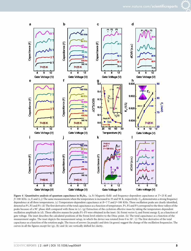
Figure 4 shows a comprehensive analysis of the quantum capacit-ance in Bi2Se3 for different experimental settings. Figure 4a demon-strates the magnetic field dependence of the total capacitance at100 KHz and 25 K. When the magnetic field increases from 3 to 9T, the low-index Landau levels with large interleave spacing progres-sively move across the Fermi level, reminiscent of typical SdH oscil-lations from transport measurements42,55 (see also SupplementaryFig. S2). Figure 4b demonstrates a clear trend of frequency-depend-ent quantum oscillations, where high frequency excitations resolvethe surface oscillations quite well. Figures 4(e,f) and 4(i,j) presentsimilar results but at higher temperatures of 35 and 50 K, respect-ively. Note that the frequency can have a significant effect on thedistinction of the surface from the bulk49,51–54, presumably because ofthe dramatic difference in carrier mobility: in the bulk, the electronmobility is approximately 380 cm2/V s, while on the surface theelectron mobility reaches over 10,000 cm2/V s (SupplementaryFigs. S2 and S6). Such a large difference enables a fast response fromthe surface states, analogous to the fast response of high-mobilityelectrons in graphene (in a gigahertz range)56; as a comparison, thebulk carriers cannot follow the high frequency excitations, result-ing in a ‘‘filtering’’ effect49,51. More importantly, the surface statescan be clearly distinguished at approximately 60 K (Fig. 4c and
Supplementary Fig. S7), much beyond the capability of the low-tem-perature transport, where movable carriers travel along horizontalchannels and are extremely sensitive to bulk properties (scatteringdetails)34. In addition, quantum capacitance probes both theextended and localized states, whereas electron transport can onlyinvestigate the former one34.
To better understand the physics behind this phenomenon, weperformed a quantitative analysis of the SdH oscillations. Figure 4cdemonstrates the temperature dependence of the total capacitancewhen the magnetic field and frequency are set to 7 T and 100 KHz,respectively. The surface states are persistent up to 60 K. Three peaksare identified, corresponding to the generation of three Landau levelsin the system. The first derivative of the total capacitance was alsotaken to remove the background parasitic capacitances (Fig. 4d). Thethree peaks from P1 to P3 have a common 90u phase shift comparedwith those in Fig. 4c. Now, we can take the amplitude of the capa-citance oscillations 2 note that the Al2O3 capacitance COX isremoved 2 and applyDC(T)=DC(0)~l(T)=sinh (l(T)), where thethermal factor is given byl(T)~2p2kBTmcycl=( eB)(refs. 5,23). Here,mcycl denotes the cyclotron mass, kB is Boltzmann’s constant, and isthe reduced Plank’s constant. By taking the conductivity oscillationamplitude and performing the best fit to the equation of DC(T)/DC(0) (Fig. 4g), mcycl is calculated to be 0.079 m0, 0.091 m0, and0.102 m0 at gate voltages of 5.9 V (P1), 8 V (P2) and 10.9 V (P3),respectively (Fig. 4g (inset)). These values are reasonably close tothose extracted from the transport measurements (0.07 m0,Supplementary Fig. S2). Here, m0 is the electron rest mass. Becausethe cyclotron mass is given by mcycl~EF=V2
F (ref. 5), where EF and VF
are the Fermi level and the Fermi velocity, both EF and VF can beprecisely obtained given mcyclVF~ kF(ref. 23). It is noted that theFermi level increases from 61.5 to 79.4 meV when the gate voltage isvaried from 15.9 to 110.9 V (Fig. 4h), exhibiting the clear gatemodulation behavior of the surface states. The kF value can also beobtained in the range of 0.025–0.033 A21, consistent with the trans-port results (Supplementary Fig. S2).
We performed a series of sample rotations under a constant mag-netic field of 7 T to identify the nature of the quantum oscillations(Fig. 4k and 4i)5,23. As the system is rotated from 0 to 50u, theamplitude of the oscillations dampens and the oscillation frequency(peak interval) changes, depending on the magnitude of B\(Fig. 4kinset), which signifies the typical 2-D characteristics of the topo-logical surface states5. The relationship between the carrier densityn and the Fermi vector kF is the same for both quadratic (2-DEG)and linear (TI surface state) E-k dispersion relations and is given byn!k2
F=p(refs. 39,57). Accordingly, the period of SdH oscillations forboth 2-DEG and TI surface states also exhibit similar behavior giventhe Onsager relation of f ~1=D(1=B)~2 pn=q(ref. 5). Therefore, itis difficult to distinguish the surface states from 2-DEG through theconventional magneto-transport measurements, which can onlyprobe the carriers that transport through the channel. However,unlike the transport approach, the quantum capacitance methodcan circumvent this challenge by providing a direct extraction ofan important quantity, dn/dVa (ref. 39, Va 2 the voltage droppedon the TI surface), which explicitly describes the surface states. Bycarefully examining their E-k relations and DOS39,57, i.e., E(k)~
vF jkj & gTI(E)~gjEj=2p( vF)2 for the surface states, E(k)~ 2k2
=2m & g2DEG(E)~mN(E)=p 2 for 2-DEG, one can theoreticallyderive and simulate their capacitances, as demonstrated in Supple-mentary Figs. S5 and S8. Here, g5gsgv is the degeneracy factor,considering both the spin and energy band degeneracies for the TIsurface states. The quantum capacitance associated with the surfacestates strongly depends on the density of states, similar to that ofgraphene34,36,37. By contrast, for 2-DEG the capacitance is saturated ata constant value irrespective of the change in Va (Supplementary Fig.S8). Therefore, the observed quantum oscillations in Figs. 3 and 4 areattributed to the surface states instead of 2-DEG, which is also
Figure 4 | Quantitative analysis of quantum capacitance in Bi2Se3. (a, b) Magnetic-field- and frequency-dependent capacitance at T525 K and
f5100 KHz. (e, f) and (i, j) The same measurements when the temperature is increased to 35 and 50 K, respectively. CQ demonstrates a strong frequency
dependence at all three temperatures. (c) Temperature-dependent capacitance at B57 T and f5100 KHz. Three oscillation peaks are clearly identified,
denoted as P1, P2 and P3. (d) The first derivative of the total capacitance as a function of temperature. P1, P2 and P3 correspond to the three valleys of the
peaks because of a 90u phase shift compared with those in (c). (g) Extraction of the cyclotron effective mass by taking the temperature-dependent
oscillation amplitude in (d). Three effective masses for peaks P1–P3 were obtained in the inset. (h) Fermi vector kF and Fermi energy EF as a function of
gate voltage. The inset describes the calculated positions of the Fermi level relative to the Dirac point. (k) The total capacitance as a function of the
measurement angles. The inset depicts the measurement setup, in which the device was rotated from 0 to 50u. (i) The first derivative of the total
capacitance as a function of the rotation angle. The traces of arrows (in purple) and dots (in green) suggest the change of the oscillation frequencies. The
curves in all the figures except for (g), (h) and (k) are vertically shifted for clarity.
verified by an ambipolar field effect in quantum capacitance(Supplementary Fig. S11).
DiscussionTo understand the frequency dependence of quantum oscillations,we carried out qualitative simulations using Technology ComputerAided Design (TCAD). A capacitor device was constructed by con-sidering the experimental conditions. Figure 5 shows that the totalcapacitance changes with the frequency of the ac signals. In essence,the capacitance for the system depends on the total available chargesunder specific measurement frequencies49,51. In the low-frequencyregime (f , 1 KHz, Fig. 5), both the bulk and surface carriers canrespond to the external ac signals, and the system can be representedby a series capacitor model (1/CT51/COX11/CQ11/CB). The bulkinterference exists in the system, and the quantum capacitance canhardly make itself distinguishable. In the high-frequency regime (f .1 KHz, Fig. 5), however, the available charges accounting for the totalcapacitance primarily originate from the surface states because thebulk carriers do not have adequate time to respond to the high acfrequencies51–54. Thus, the elimination of the bulk term leads to asignificant manifestation of the surface quantum capacitance (1/CT51/COX11/CQ). By taking two different surface carrier densities(Fig. 5, red and blue curves), we can verify the effect of the availablesurface charges on the total capacitance. In short, our simulationsprovide sensible explanations for the observed frequency dispersionof the total capacitance, although a detailed theoretical treatise is stillneeded. The discovery of the quantum capacitance in topologicalinsulators may facilitate future progress toward the creation of topo-logical devices by probing high-temperature surface states andincorporating gated structures.
MethodsMBE growth. Thin film growth was carried out with an ultra-high vacuum PerkinElmer MBE system. Si (111) substrates were cleaned using the standard RadioCorporation of America (RCA) procedure before being transferred into the growthchamber. High-purity Bi (99.9999%) and Se (99.99%) elementary sources wereevaporated by conventional effusion cells. During growth, the Bi and Se cells were
kept at 490 and 200uC, respectively, while the Si (111) substrate was kept at 150uC(growth temperature). The epitaxial growth was monitored using the in-situ RHEEDtechnique, and the surface was observed to be atomically flat, as evidenced by thestreaky RHEED patterns (Fig. 1a). Digital images of the RHEED were captured usinga KSA400 system made by K-space Associate, Inc.
Characterizations. (1) ARPES. High-resolution ARPES experiments wereperformed at beam line 12.0.1 of the Advanced Light Source at Lawrence BerkeleyNational Laboratory, using 100 eV and 52 eV photons to measure the core levels andsurface states, respectively. (2) TEM. High-resolution TEM experiments wereperformed on a Philips Tecnai F20 (S)TEM operating at 200 KV. The digital imageswere recorded by a GatanH 2k32k CCD camera. (3) Capacitance measurements.Frequency-dependent capacitance measurements were conducted with an HP/Agilent 4274A multi-frequency LCR meter. The ac frequency could be tuned from100 Hz–100 KHz, while a dc bias can be applied from 0 to 6 35 V. The LCR meterwas connected to a physical property measurement system (PPMS), where the deviceswere located. We were also able to systematically vary several experimental variablessuch as the temperature, magnetic field, measurement frequency, and external gatebias. Multiple lock-in-amplifiers and Keithley source meters were also connected tothe PPMS system, enabling comprehensive and high-sensitivity transportmeasurements for the top-gated Hall bar and capacitor devices.
Device fabrication. The MBE-grown Bi2Se3 thin film (,10 nm) was patterned into amicron-scale Hall bar geometry using conventional optical photolithography and asubsequent CHF3 dry-etching of 18 s. A 15-nm-thick, high-k Al2O3 dielectric layerwas deposited using atomic layer deposition (ALD). Hall channel contacts weredefined by e-beam evaporation after etching away Al2O3 in the contact areas. A metalstack of Fe/Al (20 nm/100 nm) was directly deposited onto the exposed Bi2Se3
surface. A top-gate metal scheme of Ti/Au (10 nm/90 nm) was achieved using asecond step of photolithography and e-beam evaporation.
Device simulation. We used a visual TCAD software package (version 1.7.3) fromCogenda.com. The simulated device structure is depicted in Fig. 5 inset. Thetopological surface is assumed to have a depth of 1 nm and carrier densities of131018 cm23 and 531018 cm23 (two scenarios). Bulk Bi2Se3 has a carrier density of6.531019–1.331020 cm23, attributed to the formation of an impurity band aselaborated in Supplementary Fig. S6. Our simplified model describes the physics offrequency-dependent capacitance in a qualitative manner. The absolute values of thetotal capacitance can be varied by altering the above parameters; however, theunderlying physics remains the same, which forms the basis of our simulations.
1. Kane, C. L. & Mele, E. J. Topological order and the quantum spin Hall effect. Phys.Rev. Lett. 95, 146802 (2005).
2. Zhang, H. et al. Topological insulators in Bi2Se3, Bi2Te3 and Sb2Te3 with a singleDirac cone on the surface. Nat. Phys. 5, 438–442 (2009).
3. Moore, J. Topological insulators: The next generation. Nat. Phys. 5, 378–380(2009).
4. Fu, L. & Kane, C. L. Topological insulators with inversion symmetry. Phys. Rev. B76, 045302 (2007).
5. Qu, D.-X., Hor, Y. S., Xiong, J., Cava, R. J. & Ong, N. P. Quantum oscillations andHall anomaly of surface states in the topological insulator Bi2Te3. Science 329,821–824 (2010).
6. Xia, Y. et al. Observation of a large-gap topological-insulator class with a singleDirac cone on the surface. Nat. Phys. 5, 398–402 (2009).
7. Zhang, T. et al. Experimental demonstration of topological surface statesprotected by time-reversal symmetry. Phys. Rev. Lett. 103, 266803 (2009).
8. Alpichshev, Z. et al. STM imaging of electronic waves on the surface ofBi2Te3:topologically protected surface states and hexagonal warping effects. Phys.Rev. Lett. 104, 016401 (2010).
9. Veldhorst, M. et al. Josephson supercurrent through a topological insulatorsurface state. Nat Mater advance online publication (2012).
10. McIver, J. W., Hsieh, D., Steinberg, H., Jarillo Herrero, P. & Gedik, N. Control overtopological insulator photocurrents with light polarization. Nat Nano 7, 96–100(2012).
11. Cho, S. et al. Topological insulator quantum dot with tunable barriers. NanoLetters 12, 469–472 (2012).
12. Bahramy, M. S., Yang, B. J., Arita, R. & Nagaosa, N. Emergence of non-centrosymmetric topological insulating phase in BiTeI under pressure. NatCommun 3, 679 (2012).
13. Arakane, T. et al. Tunable Dirac cone in the topological insulator Bi2-xSbxTe3-ySey. Nat Commun 3, 636 (2012).
14. Qi, X. L., Hughes, T. L. & Zhang, S. C. Topological field theory of time-reversalinvariant insulators. Phys. Rev. B 78, 195424 (2008).
15. Bernevig, B. A., Hughes, T. L. & Zhang, S.-C. Quantum spin Hall effect andtopological phase transition in HgTe quantum wells. Science 314, 1757–1761(2006).
16. Konig, M. et al. Quantum spin hall insulator state in HgTe quantum wells. Science318, 766–770 (2007).
17. Zhang, Y. et al. Crossover of the three-dimensional topological insulator Bi2Se3 tothe two-dimensional limit. Nat. Phys. 6, 584–588 (2010).
Figure 5 | Simulated frequency-dependent total capacitance. A device
model from the inset is constructed in accordance with the experimental
setup (Figs. 1d and 1e). During simulations, only the top surface of Bi2Se3
is considered. At low frequencies, the total capacitance exhibits a strong
dependence on frequency, primarily attributed to the sufficient responses
for the bulk and the surface carriers. When the frequency is set beyond
1 KHz, however, a desirable surface-dominant regime is attained, in which
the bulk interference is reduced at elevated frequencies. The inset depicts
18. Kou, X. F. et al. Epitaxial growth of high mobility Bi2Se3 thin films on CdS. Appl.Phys. Lett. 98, 242102 (2011).
19. Bansal, N. et al. Epitaxial growth of topological insulator Bi2Se3 film on Si(111)with atomically sharp interface. Thin Solid Films 520, 224–229 (2011).
20. Li, H. D. et al. The van der Waals epitaxy of Bi2Se3 on the vicinal Si(111) surface: anapproach for preparing high-quality thin films of a topological insulator. NewJournal of Physics 12, 103038 (2010).
21. Zhang, J. et al. Band structure engineering in (Bi12xSbx)2Te3 ternary topologicalinsulators. Nat Commun 2, 574 (2011).
22. Brahlek, M., Kim, Y. S., Bansal, N., Edrey, E. & Oh, S. Surface versus bulk state intopological insulator Bi2Se3 under environmental disorder. Appl. Phys. Lett. 99,012109 (2011).
23. Taskin, A. A., Ren, Z., Sasaki, S., Segawa, K. & Ando, Y. Observation of Dirac Holesand Electrons in a Topological Insulator. Phys. Rev. Lett. 107 (2011).
24. Kong, D. & Cui, Y. Opportunities in chemistry and materials science fortopological insulators and their nanostructures. Nat Chem 3, 845–849 (2011).
25. Xiu, F. Manipulating surface states in topological insulator nanoribbons. NatureNanotech. 6, 216–221 (2011).
26. Peng, H. et al. Topological insulator nanostructures for near-infrared transparentflexible electrodes. Nat Chem advance online publication (2012).
27. Chen, Y. L. et al. Massive Dirac Fermion on the Surface of a Magnetically DopedTopological Insulator. Science 329, 659–662 (2010).
28. Bianchi, M. et al. Coexistence of the topological state and a two-dimensionalelectron gas on the surface of Bi2Se3. Nat Commun 1, 128 (2010).
29. Cheng, P. et al. Landau quantization of topological surface states in Bi2Se3. Phys.Rev. Lett. 105, 076801 (2010).
30. Steinberg, H., Gardner, D. R., Lee, Y. S. & Jarillo-Herrero, P. Surface StateTransport and Ambipolar Electric Field Effect in Bi2Se3 Nanodevices. NanoLetters 10, 5032–5036 (2010).
31. Analytis, J. G. et al. Two-dimensional surface state in the quantum limit of atopological insulator. Nat. Phys. 6, 960–964 (2010).
32. Sacepe, B. et al. Gate-tuned normal and superconducting transport at the surfaceof a topological insulator. Nat Commun 2, 575 (2011).
33. Chen, J. et al. Gate-Voltage Control of Chemical Potential and WeakAntilocalization in Bi2Se3. Phys. Rev. Lett. 105, 176602 (2010).
34. Ponomarenko, L. A. et al. Density of States and Zero Landau Level Probed throughCapacitance of Graphene. Phys. Rev. Lett. 105, 136801 (2010).
35. Luryi, S. Quantum capacitance devices. Appl. Phys. Lett. 52, 501–503 (1988).36. Xu, H. et al. Quantum Capacitance Limited Vertical Scaling of Graphene Field-
Effect Transistor. ACS Nano 5, 2340–2347 (2011).37. Xia, J., Chen, F., Li, J. & Tao, N. Measurement of the quantum capacitance of
graphene. Nat Nano 4, 505–509 (2009).38. Ilani, S., Donev, L. A. K., Kindermann, M. & McEuen, P. L. Measurement of the
quantum capacitance of interacting electrons in carbon nanotubes. Nat Phys 2,687–691 (2006).
39. John, D. L., Castro, L. C. & Pulfrey, D. L. Quantum capacitance in nanoscale devicemodeling. J. Appl. Phys. 96, 5180–5184 (2004).
40. Giannazzo, F., Sonde, S., Raineri, V. & Rimini, E. Screening Length and QuantumCapacitance in Graphene by Scanning Probe Microscopy. Nano Letters 9, 23–29(2008).
41. Guo, J., Yoon, Y. & Ouyang, Y. Gate Electrostatics and Quantum Capacitance ofGraphene Nanoribbons. Nano Letters 7, 1935–1940 (2007).
42. Henriksen, E. A. & Eisenstein, J. P. Measurement of the electronic compressibilityof bilayer graphene. Phys. Rev. B 82, 041412 (2010).
43. Droscher, S. et al. Quantum capacitance and density of states of graphene. Appl.Phys. Lett. 96, 152104 (2010).
44. Cho, S., Butch, N. P., Paglione, J. & Fuhrer, M. S. Insulating Behavior in UltrathinBismuth Selenide Field Effect Transistors. Nano Letters 11, 1925–1927 (2011).
45. Yu, R. et al. Quantized Anomalous Hall Effect in Magnetic Topological Insulators.Science 329, 61–64 (2010).
46. Kim, Y. S. et al. Thickness-dependent bulk properties and weak antilocalizationeffect in topological insulator Bi_{2}Se_{3}. Phys. Rev. B 84, 073109 (2011).
47. Hsieh, D. et al. A tunable topological insulator in the spin helical Dirac transportregime. Nature 460, 1101–1105 (2009).
48. Kordyuk, A. A. et al. Photoemission-induced gating of topological insulators.Phys. Rev. B 83, 081303 (2011).
49. Sze, S. Physics of Semiconductor Devices, 3rd ed. (Wiley, New York, 2007).50. Lind, E., Niquet, Y.-M., Mera, H. & Wernersson, L.-E. Accumulation capacitance
of narrow band gap metal-oxide-semiconductor capacitors. Appl. Phys. Lett. 96,233507 (2010).
51. Bulbul, M. M. & Zeyrek, S. Frequency dependent capacitance and conductance–voltage characteristics of Al/Si3N4/p-Si(100) MIS diodes. MicroelectronicEngineering 83, 2522–2526 (2006).
52. Lieneweg, U. Frequency response of charge transfer in MOS inversion layers.Solid-State Electronics 23, 577–583 (1980).
53. Xuan, Y., Lin, H. C., Ye, P. D. & Wilk, G. D. Capacitance-voltage studies onenhancement-mode InGaAs metal-oxide-semiconductor field-effect transistorusing atomic-layer-deposited Al[sub 2]O[sub 3] gate dielectric. Appl. Phys. Lett.88, 263518 (2006).
54. Jiang, J., Awadelkarim, O. O., Lee, D. O., Roman, P. & Ruzyllo, J. On thecapacitance of metal/high-k dielectric material stack/silicon structures. Solid-State Electronics 46, 1991–1995 (2002).
55. Zhang, Y., Tan, Y.-W., Stormer, H. L. & Kim, P. Experimental observation of thequantum Hall effect and Berry’s phase in graphene. Nature 438, 201–204 (2005).
56. Liao, L. et al. High-speed graphene transistors with a self-aligned nanowire gate.Nature 467, 305-308 (2010).
57. Fang, T., Konar, A., Xing, H. & Jena, D. Carrier statistics and quantum capacitanceof graphene sheets and ribbons. Appl. Phys. Lett. 91, 092109 (2007).
AcknowledgementsF.X. would like to acknowledge the financial support received from the National ScienceFoundation under the Award No. 1201883, and the College of Engineering at Iowa StateUniversity. The Microelectronics Research Center at Iowa State provided substantialequipment supports during the project. F.X., K.W. Y.W. and J.Z. would like to thank theFocus Center Research Program-Center on Functional Engineered Nano Architectonics(FENA), the Australia Research Council. Y.W. would like to thank National ScienceFoundation of China (No. 11174244) for the financial support received for this project. F.X.would like to acknowledge Mingqiang Bao for setting up the CV measurement system, PengZhang for helpful discussions on ARPES, and Shen Chen for extensive guidance on theusage of the Visual TCAD software.
Author contributionsF.X. conceived and designed the research. F.X., X.K. and M.L. fabricated the capacitordevices and performed the measurements. L.H., M.L. and X.Y. contributed to themeasurements and analysis. Y.W. and J.Z. performed structural analysis. A.V. provided theARPES measurements. X.K. and F.X. performed numerical simulations on capacitances.F.X., N.M. and X.K. wrote the paper, with help from all the other co-authors.
Additional informationReprints and permission information is available online at http://npg.nature.com/reprintsandpermissions.
Supplementary information accompanies this paper at http://www.nature.com/scientificreports
Competing financial interests: The authors declare no competing financial interests.
License: This work is licensed under a Creative CommonsAttribution-NonCommercial-ShareAlike 3.0 Unported License. To view a copy of thislicense, visit http://creativecommons.org/licenses/by-nc-sa/3.0/
How to cite this article: Xiu, F. et al. Quantum Capacitance in Topological Insulators. Sci.Rep. 2, 669; DOI:10.1038/srep00669 (2012).