Quartus ® II Introduction for VHDL Users This tutorial presents an introduction to the Quartus ® II software. It gives a general overview of a typical CAD flow for designing circuits that are implemented by using FPGA devices, and shows how this flow is realized in the Quartus ® II software. The design process is illustrated by giving step-by-step instructions for using the Quartus ® II software to implement a simple circuit in an Altera ® FPGA device. The Quartus ® II system includes full support for all of the popular methods of entering a description of the desired circuit into a CAD system. This tutorial makes use of the VHDL design entry method, in which the user specifies the desired circuit in the VHDL hardware description language. Another version of this tutorial is available that uses Verilog hardware description language. The screen captures in the tutorial were obtained using Quartus ® II version 10.0; if other versions of the soft- ware are used, some of the images may be slightly different. Contents: Getting Started Starting a New Project Design Entry Using VHDL Code Compiling the VHDL Code Using the RTL Viewer Specifying Timing Constraints Quartus ® II Windows
Transcript
Quartus® II Introduction for VHDL Users
This tutorial presents an introduction to the Quartus® II software. It gives a general overview of a typical CADflow for designing circuits that are implemented by using FPGA devices, and shows how this flow is realized in theQuartus® II software. The design process is illustrated by giving step-by-step instructions for using the Quartus®
II software to implement a simple circuit in an Altera® FPGA device.The Quartus® II system includes full support for all of the popular methods of entering a description of the
desired circuit into a CAD system. This tutorial makes use ofthe VHDL design entry method, in which theuser specifies the desired circuit in the VHDL hardware description language. Another version of this tutorial isavailable that uses Verilog hardware description language.
The screen captures in the tutorial were obtained using Quartus® II version 10.0; if other versions of the soft-ware are used, some of the images may be slightly different.
Contents:Getting StartedStarting a New ProjectDesign Entry Using VHDL CodeCompiling the VHDL CodeUsing the RTL ViewerSpecifying Timing ConstraintsQuartus® II Windows
Computer Aided Design (CAD) software makes it easy to implement a desired logic circuit by using a pro-grammable logic device, such as a field-programmable gate array (FPGA) chip. A typical FPGA CAD flow isillustrated in Figure 1.
Design correct?
Functional Simulation
No
Yes
Synthesis
Timing requirements met?
Fitting
Timing Analysis and Simulation
Programming and Configuration
Yes
No
Design Entry
Figure 1: Typical CAD flow.
It involves the following basic steps:
• Design Entry – the desired circuit is specified either by using a hardware description language, such asVerilog or VHDL, or by means of a schematic diagram
• Synthesis– the CAD Synthesis tool synthesizes the circuit into a netlist that gives the logic elements (LEs)needed to realize the circuit and the connections between the LEs
• Functional Simulation – the synthesized circuit is tested to verify its functionalcorrectness; the simulationdoes not take into account any timing issues
• Fitting – the CAD Fitter tool determines the placement of the LEs defined in the netlist into the LEs inan actual FPGA chip; it also chooses routing wires in the chipto make the required connections betweenspecific LEs
• Timing Analysis – propagation delays along the various paths in the fitted circuit are analyzed to providean indication of the expected performance of the circuit
ALTERA® CORPORATION
MAY 20102
QUARTUS® II I NTRODUCTION FORVHDL U SERS
• Timing Simulation – the fitted circuit is tested to verify both its functional correctness and timing
• Programming and Configuration – the designed circuit is implemented in a physical FPGA chipby pro-gramming the configuration switches that configure the LEs and establish the required wiring connections
This tutorial introduces the basic features of the Quartus® II software. It shows how the software can be usedto design and implement a circuit specified using the VHDL hardware description language. It makes use of thegraphical user interface to invoke the Quartus® II commands. During this tutorial, the reader will learn about:
• Creating a project
• Synthesizing a circuit from VHDL code using the Quartus® II Integrated Synthesis tool
• Fitting a synthesized circuit into an Altera® FPGA
• Examining the report on the results of fitting and timing analysis
• Examining the synthesized circuit in the form of a schematic diagram generated by the RTL Viewer tool
• Making simple timing assignments in the Quartus® II software
ALTERA® CORPORATION
MAY 20103
QUARTUS® II I NTRODUCTION FORVHDL U SERS
1 GETTING STARTED
1 Getting Started
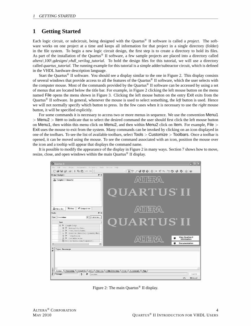
Each logic circuit, or subcircuit, being designed with the Quartus® II software is called aproject. The soft-ware works on one project at a time and keeps all information for that project in a single directory (folder)in the file system. To begin a new logic circuit design, the first step is to create a directory to hold its files.As part of the installation of the Quartus® II software, a few sample projects are placed into a directory calledaltera\100\qdesigns\vhdl_verilog_tutorial. To hold the design files for this tutorial, we will use a directorycalledquartus_tutorial. The running example for this tutorial is a simple adder/subtractor circuit, which is definedin the VHDL hardware description language.
Start the Quartus® II software. You should see a display similar to the one in Figure 2. This display consistsof several windows that provide access to all the features ofthe Quartus® II software, which the user selects withthe computer mouse. Most of the commands provided by the Quartus® II software can be accessed by using a setof menus that are located below the title bar. For example, inFigure 2 clicking the left mouse button on the menunamedFile opens the menu shown in Figure 3. Clicking the left mouse button on the entryExit exits from theQuartus® II software. In general, whenever the mouse is used to selectsomething, theleft button is used. Hencewe will not normally specify which button to press. In the fewcases when it is necessary to use theright mousebutton, it will be specified explicitly.
For some commands it is necessary to access two or more menus in sequence. We use the conventionMenu1> Menu2 > Item to indicate that to select the desired command the user should first click the left mouse buttonon Menu1, then within this menu click onMenu2, and then withinMenu2 click on Item. For example,File >
Exit uses the mouse to exit from the system. Many commands can be invoked by clicking on an icon displayed inone of the toolbars. To see the list of available toolbars, selectTools > Customize > Toolbars. Once a toolbar isopened, it can be moved using the mouse. To see the command associated with an icon, position the mouse overthe icon and a tooltip will appear that displays the command name.
It is possible to modify the appearance of the display in Figure 2 in many ways. Section 7 shows how to move,resize, close, and open windows within the main Quartus® II display.
Figure 2: The main Quartus® II display.
ALTERA® CORPORATION
MAY 20104
QUARTUS® II I NTRODUCTION FORVHDL U SERS
1 GETTING STARTED 1.1 Quartus® II Online Help
Figure 3: An example of the File menu.
1.1 Quartus® II Online Help
The Quartus® II software provides comprehensive online documentation that answers many of the questions thatmay arise when using the software. The documentation is accessed from the menu in theHelp window. To getsome idea of the extent of documentation provided, it is worthwhile for the reader to browse through theHelpmenu.
The user can quickly search through the Help topics by selecting Help > Search, which opens a dialog boxinto which keywords can be entered. Another method, context-sensitive help, is provided for quickly findingdocumentation about specific topics. While using most applications, pressing theF1 function key on the keyboardopens a Help display that shows the commands available for the application.
ALTERA® CORPORATION
MAY 20105
QUARTUS® II I NTRODUCTION FORVHDL U SERS
2 STARTING A NEW PROJECT
2 Starting a New Project
To start working on a new design we first have to define a newdesign project. The Quartus® II software makesthe designer’s task easy by providing support in the form of awizard.
1. SelectFile > New Project Wizard to reach a window that indicates the capability of this wizard. PressNext. This will bring up the wizard screen as shown in Figure 4.
Figure 4: Creation of a new project.
2. Set the working directory to bequartus_tutorial; of course, you can use a directory name of your choice.The project must have a name, which is usually the same as the top-level design entity that will be includedin the project. Chooseaddersubtractoras the name for both the project and the top-level entity, as shown inFigure 4. PressNext. Since we have not yet created the directoryquartus_tutorial, the Quartus® II softwaredisplays the pop-up box in Figure 5 asking if it should createthe desired directory. ClickYes, which leadsto the window in Figure 6.
Figure 5: The Quartus® II software can create a new directory for the project.
ALTERA® CORPORATION
MAY 20106
QUARTUS® II I NTRODUCTION FORVHDL U SERS
2 STARTING A NEW PROJECT
Figure 6: The wizard can include user-specified design files.
3. This window makes it easy to specify which existing files (if any) should be included in the project. Assum-ing that we do not have any existing files, clickNext, which leads to the window in Figure 7.
ALTERA® CORPORATION
MAY 20107
QUARTUS® II I NTRODUCTION FORVHDL U SERS
2 STARTING A NEW PROJECT
Figure 7: Choose the device family and a specific device.
4. In this window, we can specify the type of device in which the designed circuit will be implemented. Choosethe Stratix III® menu item as the target device family. We can let the Quartus® II software select a specificdevice in the family, or we can choose the device explicitly.We will take the latter approach. From the listof available devices, choose the device called EP3SE50F484C2. PressNext, which opens the window inFigure 8.
ALTERA® CORPORATION
MAY 20108
QUARTUS® II I NTRODUCTION FORVHDL U SERS
2 STARTING A NEW PROJECT
Figure 8: Other EDA tools can be specified.
5. In this window we can specify any third-party tools that should be used. A commonly used term for CADsoftware for electronic circuits isEDA tools, where the acronym stands for Electronic Design Automation.This term is used in the Quartus® II messages that refer to third-party tools, which are the tools developedand marketed by companies other than Altera®; other tutorials show how such tools may be used. Since wewill rely solely on the Quartus® II tools, we will not choose any other tools. PressNext. Now, a summaryof the chosen settings appears in the screen shown in Figure 9. PressFinish, which returns to the mainQuartus® II display. Note thataddersubtractoris now specified as the current project, as indicated in thetitle bar at the top of the display. The screen should look similar to that of Figure 10.
ALTERA® CORPORATION
MAY 20109
QUARTUS® II I NTRODUCTION FORVHDL U SERS
2 STARTING A NEW PROJECT
Figure 9: Summary of the project settings.
Figure 10: The Quartus® II display for the created project.
ALTERA® CORPORATION
MAY 201010
QUARTUS® II I NTRODUCTION FORVHDL U SERS
3 DESIGN ENTRY USING VHDL CODE
3 Design Entry Using VHDL Code
As a design example, we will use the adder/subtractor circuit shown in Figure 11. The circuit can add, subtract, andaccumulaten-bit numbers using the 2’s complement number representation. The two primary inputs are numbersA = an−1an−2 · · · a0 andB = bn−1bn−2 · · · b0, and the primary output isZ = zn−1zn−2 · · · z0. Another inputis theAddSubcontrol signal which causesZ = A + B to be performed whenAddSub= 0 andZ = A − B whenAddSub= 1. A second control input,Sel, is used to select the accumulator mode of operation. IfSel= 0, theoperationZ = A ± B is performed, but ifSel= 1, thenB is added to or subtracted from the current value ofZ.If the addition or subtraction operations result in arithmetic overflow, an output signal,Overflow, is asserted.
To make it easier to deal with asynchronous input signals, wewill load them into flip-flops on a positive edgeof the clock. Thus, inputsA andB will be loaded into registersAreg andBreg, while SelandAddSubwill beloaded into flip-flopsSelRandAddSubR, respectively. The adder/subtractor circuit places the result into registerZreg.
m0mn 1–
a0an 1–
n-bit adder
n-bit register
F/F
n-bit register
F/F
areg0aregn 1–
n-bit register
z0zn 1–
g0gn 1–
n-bit 2-to-1 MUX
A =
G =
M =
Z =
Areg = breg0bregn 1–Breg =
SelR
carryin
b0bn 1–B =
h0hn 1–H =
Sel AddSub
hn 1–
carryout
F/F
Overflow
AddSubR
Zreg
zreg0zregn 1–Zreg =over_flow
Figure 11: The adder/subtractor circuit.
The required circuit is described by the VHDL code in Figure 12. For our example, we will use a 16-bit circuitas specified byn = 16.
ALTERA® CORPORATION
MAY 201011
QUARTUS® II I NTRODUCTION FORVHDL U SERS
3 DESIGN ENTRY USING VHDL CODE
LIBRARY ieee ;USE ieee.std_logic_1164.all ;
-- Top-level entityENTITY addersubtractor IS
GENERIC ( n : INTEGER := 16 ) ;PORT ( A, B : IN STD_LOGIC_VECTOR(n-1 DOWNTO 0) ;
Clock, Reset, Sel, AddSub : IN STD_LOGIC ;Z : BUFFER STD_LOGIC_VECTOR(n-1 DOWNTO 0) ;Overflow : OUT STD_LOGIC ) ;
Figure 12. VHDL code for the circuit in Figure 11 (Partb).
Note that the top VHDL entity is calledaddersubtractorto match the name given in Figure 4, which was specifiedwhen the project was created. This code can be typed into a fileby using any text editor that stores ASCII files, orby using the Quartus® II text editing facilities. While the file can be given any name, it is a common designers’practice to use the same name as the name of the top-level VHDLentity. The file name must include the extensionvhd, which indicates a VHDL file. So, we will use the nameaddersubtractor.vhd. For convenience, we provide therequired file in the directoryaltera\100\qdesigns\vhdl_verilog_tutorial. Copy this file into the project directoryquartus_tutorial.
ALTERA® CORPORATION
MAY 201013
QUARTUS® II I NTRODUCTION FORVHDL U SERS
3 DESIGN ENTRY USING VHDL CODE 3.1 Using the Quartus® II Text Editor
3.1 Using the Quartus® II Text Editor
This section demonstrates how to use the Quartus® II Text Editor. You can skip this section if you prefer touse some other text editor to create theaddersubtractor.vhdfile, or if you have chosen to copy the file from thealtera\100\qdesigns\vhdl_verilog_tutorialdirectory.
1. SelectFile > New to get the window in Figure 13, chooseVHDL File, and clickOK. This opens the TextEditor window.
Figure 13: Choose to prepare a VHDL file.
2. The first step is to specify a name for the file that will be created. SelectFile > Save As to open the pop-upbox shown in Figure 14. In the field labeledSave as type chooseVHDL File. In the field labeledFilename typeaddersubtractor. Put a checkmark in the boxAdd file to current project. Click Save, whichputs the file into the directoryquartus_tutorialand leads to the Text Editor window shown in Figure 15.
ALTERA® CORPORATION
MAY 201014
QUARTUS® II I NTRODUCTION FORVHDL U SERS
3 DESIGN ENTRY USING VHDL CODE 3.1 Using the Quartus® II Text Editor
Figure 14: Name the file.
Figure 15: Text Editor window.
ALTERA® CORPORATION
MAY 201015
QUARTUS® II I NTRODUCTION FORVHDL U SERS
3 DESIGN ENTRY USING VHDL CODE 3.2 Adding Design Files to a Project
3. Enter the VHDL code in Figure 12 into the Text Editor Window, which is located on the right side of thescreen. Save the file by going toFile > Save, or by typing the shortcutCtrl-s.
Most of the commands available in the Text Editor are self-explanatory. Text is entered at theinsertion point,which is indicated by a thin vertical line. The insertion point can be moved either by using the keyboard arrowkeys or by using the mouse. Two features of the Text Editor areespecially convenient for typing VHDL code.First, the editor can display different types of VHDL statements in different colors, which is the default choice.Second, the editor can automatically indent the text on a newline so that it matches the previous line. Such optionscan be controlled by the settings inTools > Options > Text Editor, as shown in Figure 16.
Figure 16: Text Editor Options.
3.1.1 Using VHDL Templates
The syntax of VHDL code is sometimes difficult for a designer to remember. To help with this issue, the TextEditor provides a collection ofVHDL templates. The templates provide examples of various types of VHDLstatements, such as anentity declaration, aprocessstatement, and assignment statements. It is worthwhile tobrowse through the templates by selectingEdit > Insert Template > VHDL to become familiar with theseresources.
3.2 Adding Design Files to a Project
As we indicated when discussing Figure 6, you can tell the Quartus® II software which design files it shoulduse as part of the current project. To see the list of files already included in theaddersubtractorproject, selectAssignments > Settings > Files, which leads to a window similar to the window in Figure 17. Analternativeway of making this selection is to go toProject > Add/Remove Files in Project.
If you used the Quartus® II Text Editor to create the file and checked the box labeledAdd file to currentproject, as described in Section 3.1, then theaddersubtractor.vhdfile is already a part of the project and will belisted in the window in Figure 17. Otherwise, the file must be added to the project.
ALTERA® CORPORATION
MAY 201016
QUARTUS® II I NTRODUCTION FORVHDL U SERS
3 DESIGN ENTRY USING VHDL CODE 3.2 Adding Design Files to a Project
Figure 17: Settings window.
1. If not already done, place a copy of the fileaddersubtractor.vhdinto the directoryquartus_tutorialby gettingit from the directoryaltera\100\qdesigns\vhdl_verilog_tutorial, or by using a file that you created usinganother text editor.
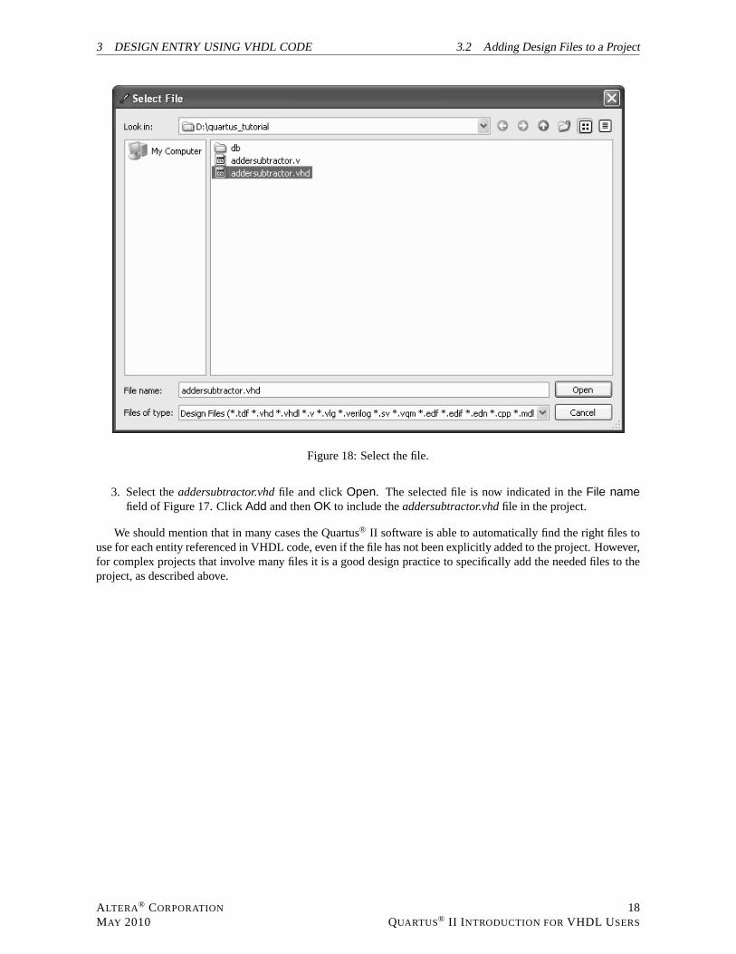
2. To add this file to the project, click on the... button beside theFile name field in Figure 17 to get thepop-up window in Figure 18.
ALTERA® CORPORATION
MAY 201017
QUARTUS® II I NTRODUCTION FORVHDL U SERS
3 DESIGN ENTRY USING VHDL CODE 3.2 Adding Design Files to a Project
Figure 18: Select the file.
3. Select theaddersubtractor.vhdfile and clickOpen. The selected file is now indicated in theFile namefield of Figure 17. ClickAdd and thenOK to include theaddersubtractor.vhdfile in the project.
We should mention that in many cases the Quartus® II software is able to automatically find the right files touse for each entity referenced in VHDL code, even if the file has not been explicitly added to the project. However,for complex projects that involve many files it is a good design practice to specifically add the needed files to theproject, as described above.
ALTERA® CORPORATION
MAY 201018
QUARTUS® II I NTRODUCTION FORVHDL U SERS
4 COMPILING THE VHDL CODE
4 Compiling the VHDL Code
The VHDL code is processed by several Quartus® II tools that analyze the code and generate an implementationof it for the target chip. These tools are controlled by the application program called theCompiler.
1. Run the Compiler by selectingProcessing > Start Compilation, or by using the toolbar icon . As thecompilation moves through various stages, its progress is reported in the Tasks window on the left side.This window also provides an comprehensive interface to edit, start and monitor different stages of thecompilation. Successful (or unsuccessful) compilation isindicated in a pop-up box. Acknowledge it byclicking OK. This leads to the Quartus® II display in Figure 19, in which we have expanded the Entityhierarchy in the top left corner to show all entities in theaddersubtractordesign. In the message window,located at the bottom of the display, various messages are shown. In case of errors, there will be appropriatemessages given.
Figure 19: Display after a successful compilation.
2. When the compilation is finished, a compilation report is produced. A window showing this report, dis-played in Figure 20, is opened automatically. The window canbe resized, maximized, or closed in thenormal way, and it can be opened at any time either by selecting Processing > Compilation Report or
by clicking on the icon in the toolbar. The report includes a number of sections listed on the left sideof its window. Figure 20 shows the Compiler Flow Summary section, which indicates that only a minisculeamount of chip resources are needed to implement this tiny circuit on the selected FPGA chip.
ALTERA® CORPORATION
MAY 201019
QUARTUS® II I NTRODUCTION FORVHDL U SERS
4 COMPILING THE VHDL CODE
Figure 20: Compilation report.
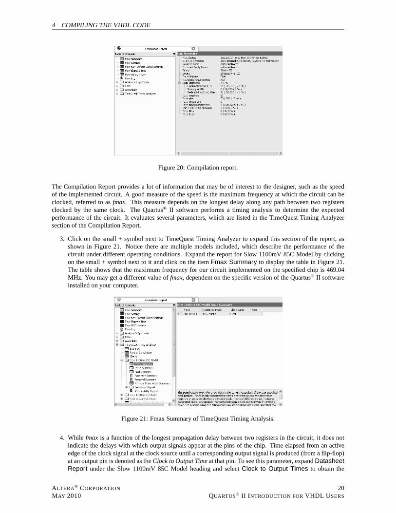
The Compilation Report provides a lot of information that may be of interest to the designer, such as the speedof the implemented circuit. A good measure of the speed is themaximum frequency at which the circuit can beclocked, referred to asfmax. This measure depends on the longest delay along any path between two registersclocked by the same clock. The Quartus® II software performs a timing analysis to determine the expectedperformance of the circuit. It evaluates several parameters, which are listed in the TimeQuest Timing Analyzersection of the Compilation Report.
3. Click on the small + symbol next to TimeQuest Timing Analyzer to expand this section of the report, asshown in Figure 21. Notice there are multiple models included, which describe the performance of thecircuit under different operating conditions. Expand the report for Slow 1100mV 85C Model by clickingon the small + symbol next to it and click on the itemFmax Summary to display the table in Figure 21.The table shows that the maximum frequency for our circuit implemented on the specified chip is 469.04MHz. You may get a different value offmax, dependent on the specific version of the Quartus® II softwareinstalled on your computer.
Figure 21: Fmax Summary of TimeQuest Timing Analysis.
4. While fmax is a function of the longest propagation delay between two registers in the circuit, it does notindicate the delays with which output signals appear at the pins of the chip. Time elapsed from an activeedge of the clock signal at the clock source until a corresponding output signal is produced (from a flip-flop)at an output pin is denoted as theClock to Output Timeat that pin. To see this parameter, expandDatasheetReport under the Slow 1100mV 85C Model heading and selectClock to Output Times to obtain the
ALTERA® CORPORATION
MAY 201020
QUARTUS® II I NTRODUCTION FORVHDL U SERS
4 COMPILING THE VHDL CODE
display in Figure 22. For each output signal, the delays for rise edge and fall edge are listed. The clocksignal and its active edge are also shown in the table. Two other parameters listed in the Datasheet ReportareSetup TimesandHold Times. TheSetup Timemeasures the length of time for which data that feeds aregister must be present at an input pin before the clock signal is asserted at the clock pin. TheHold Timemeasures the minimum length of time for which data that feedsa register must be retained at an input pinafter the clock signal is asserted at the clock pin.
Figure 22: TheClock to Output Timedelays.
5. An indication of where the circuit is implemented on the chip is available by selectingTools > ChipPlanner(Floorplan and Chip Editor), or by clicking on the icon . This opens the Chip Planner display,as shown in Figure 23. This display highlights the location of the logic elements used to implement thecircuit. To make the image appear as shown in Figure 23 you mayhave to selectView > Fit in Window(shortcutCtrl-Alt-w).
Figure 23: View of the floorplan.
6. A Zoom Tool, activated by the icon in the left hand toolbar, can be used to enlarge parts of the imageeven more. You can click and drag a box over an area of the chip to quickly zoom into that part of the chip.Figure 24 shows a zoomed-in view of the floorplan that highlights the implemented circuit. By positioningthe cursor on any logic element, the designer can see what part of the circuit is implemented in this resource.The chip planner tool has several icons that can be used to view aspects such as fan-in and fan-out of nodes,
ALTERA® CORPORATION
MAY 201021
QUARTUS® II I NTRODUCTION FORVHDL U SERS
4 COMPILING THE VHDL CODE 4.1 Errors
connecting paths between nodes, and so on. For more information on using this tool, refer to Help byselectingHelp > Search > Contents > Achieving Timing Closure > Working With Assignments inthe Chip Planner from the main Quartus® II display.
Figure 24: A portion of the expanded view.
4.1 Errors
The Quartus® II software displays messages produced during compilationin the Messages window. If the VHDLdesign file is correct, one of the messages will state that thecompilation was successful and that there are no errors.
If the Compiler does not report zero errors, then there is at least one mistake in the VHDL code. In this casea message corresponding to each error found will be displayed in the Messages window. Double-clicking on anerror message will highlight the offending statement in theVHDL code in the Text Editor window. Similarly, theCompiler may display some warning messages. Their details can be explored in the same way as in the case oferror messages. The user can obtain more information about aspecific error or warning message by selecting themessage and pressing theF1 function key.
1. To see the effect of an error, open the fileaddersubtractor.vhd. Line 57 has the statement
H <= Breg XOR AddSubR_n ;
Replace H with J in this statement, illustrating a typographical error that is easily made because H and J areadjacent on the keyboard. Compile the erroneous design file.Quartus® II software will display a pop-upbox indicating that the compilation was not successful. Acknowledge it by clickingOK. The compilationreport summary, given in Figure 25, now confirms the failed result.
Figure 25: Compilation report for the failed design.
2. In this window, Click onAnalysis & Synthesis > Messages to have all messages displayed as shown inFigure 26.
ALTERA® CORPORATION
MAY 201022
QUARTUS® II I NTRODUCTION FORVHDL U SERS
4 COMPILING THE VHDL CODE 4.1 Errors
Figure 26: Error messages.
3. Double-click on the first error message, which states thatvariable J is not declared. The Quartus® II softwareresponds by opening theaddersubtractor.vhdfile and highlighting the erroneous statement as shown inFigure 27. Correct the error and recompile the design.
Figure 27: Identifying the location of the error.
ALTERA® CORPORATION
MAY 201023
QUARTUS® II I NTRODUCTION FORVHDL U SERS
5 USING THE RTL VIEWER
5 Using the RTL Viewer
The Quartus® II software includes a tool that can display a schematic diagram of the designed circuit. The displayis at the Register Transfer Level of detail, and the tool is called theRTL Viewer.
1. Click Tools > Netlist Viewers > RTL Viewer, to reach the window shown in Figure 28.
Figure 28: Theaddersubtractorcircuit displayed by the RTL Viewer.
The displayed image shows the structure of the entireaddersubtractorcircuit. The inputs to the circuit, shownon the left side, are registered. The two subcircuits, defined by themux2to1andadderkmodules, are drawn asshaded boxes and their respective names appear above the boxes. The remainder of the circuit are the XOR gatesused to complement theB vector when subtraction is performed, and the circuitry needed to generate theOverflowsignal.
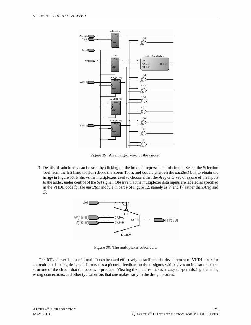
2. Use the Zoom Tool, located in the left hand toolbar, to enlarge the image and view the upper-left portion ofthe circuit, as illustrated in Figure 29. Note that individual flip-flops are used for theAddSubandSelsignals.Sixteen-bit vectorsA andB are denoted by heavy lines connected to the registers,AregandBreg, which areindicated as heavily outlined flip-flop symbols. TheZreg register is drawn in the same manner asAregandBreg.
ALTERA® CORPORATION
MAY 201024
QUARTUS® II I NTRODUCTION FORVHDL U SERS
5 USING THE RTL VIEWER
Figure 29: An enlarged view of the circuit.
3. Details of subcircuits can be seen by clicking on the box that represents a subcircuit. Select the SelectionTool from the left hand toolbar (above the Zoom Tool), and double-click on themux2to1box to obtain theimage in Figure 30. It shows the multiplexers used to choose either theAregor Z vector as one of the inputsto the adder, under control of theSelsignal. Observe that the multiplexer data inputs are labeled as specifiedin the VHDL code for themux2to1module in partb of Figure 12, namely asV andW rather thanAregandZ.
Figure 30: The multiplexer subcircuit.
The RTL viewer is a useful tool. It can be used effectively to facilitate the development of VHDL code fora circuit that is being designed. It provides a pictorial feedback to the designer, which gives an indication of thestructure of the circuit that the code will produce. Viewingthe pictures makes it easy to spot missing elements,wrong connections, and other typical errors that one makes early in the design process.
ALTERA® CORPORATION
MAY 201025
QUARTUS® II I NTRODUCTION FORVHDL U SERS
6 SPECIFYING TIMING CONSTRAINTS
6 Specifying Timing Constraints
The Quartus® II software allows the user to specify timing constraints for the designed circuit.
1. Open TimeQuest Timing Analyzer by selectingTools > TimeQuest Timing Analyzer, or by clicking
the icon . Figure 31 shows the interface of TimeQuest Timing Analyzer. It is a very powerful tool forthe designer to create, manage, and analyze timing constraints, and to quickly perform timing verificationfor their design. The compilation in Section 4 produced thefmaxof 469.04 MHz, which translates to aminimumperiodof 2.1320ns. Suppose that we need a circuit that can operate at a clock frequency of 475MHz. We can use the TimeQuest Timing Analyzer tool to create anew SDC (Synopsys Design Constraints)file containing the clock constraint.
Figure 31: TimeQuest Timing Analyzer.
In the TimeQuest Analyzer window, double clickCreate Timing Netlist under the Tasks heading to gen-erate the timing netlist from database created after compilation. Then selectConstraints > Create Clockfrom the menu to reach the dialog box in Figure 32. Specify a name for the clock you want to constrain.This name can be used to refer to this clock when creating other timing constraints. For this example, wewill name the clock "CLOCK". As we want the circuit to operateat a clock frequency of 475 MHz, set theperiod to 2.10 ns in thePeriod field. To specify the actual clock this constraint is appliedto, click on the...button beside theTargets field in the Create Clock window to get the pop-up window in Figure 33.
Figure 32: Create clock constraints.
ALTERA® CORPORATION
MAY 201026
QUARTUS® II I NTRODUCTION FORVHDL U SERS
6 SPECIFYING TIMING CONSTRAINTS
Figure 33: Choose target clock.
Click on thelist button in the middle left of the window to get a list of all the ports. SelectClock fromthe list of matches on the left and click on the> button to reach the display in Figure 33. This tells theTimeQuest Timing Analyzer to constrain theClock port to the period you have specified. Notice in a largerdesign with many ports, we can enter the name of the port in theFilter field located in the top right of thewindow to reduce the number of matches in our search. ClickOK to return to the dialog box in Figure 34.
Figure 34: Complete clock constraint.
In theSDC command field at the bottom of the dialog box in Figure 34, we can see theactual commandthat would be written into the SDC file. It creates a simple clock named CLOCK with a 2.10 ns periodand associates this constraint with the portClock. Click Run to return to the window in Figure 31. Se-lect Constraints > write SDC File and save the file asaddersubtractor.out.sdcin the project directoryquartus_tutorial. Close the TimeQuest Timing Analyzer window to return to theQuartus® II main display.
2. From the main Quartus® II window, click Assignments > Settings > Timing Analysis Settings andselect"Use TimeQuest Timing Analyzer during compilation". Expand theTiming Analysis Settingscategory and then click onTimeQuest Timing Analyzer to reach the window in Figure 35. Here, we canadd the SDC file we have created to the project. Click on the... button beside theSDC filename field andselectaddersubtractor.out.sdc, which is the SDC file we created using TimeQuest Timing Analyzer. Clickon Open to return to the window in Figure 35 and clickAdd to associate the SDC file with this project.Click OK to return to the main Quartus® II window.
ALTERA® CORPORATION
MAY 201027
QUARTUS® II I NTRODUCTION FORVHDL U SERS
6 SPECIFYING TIMING CONSTRAINTS
Figure 35: Adding SDC file to project.
The Quartus® II Compiler includes a Fitter executable that places the designed circuit into the availablelogic elements on the chip and generates the necessary wiring connections to realize the circuit. This is acomplex process that can take a long time, particularly if the circuit is large and an ambitious value offmaxis specified. The time can be reduced if a lower value offmaxis acceptable. The user can indicate the levelof the Fitter’s effort.
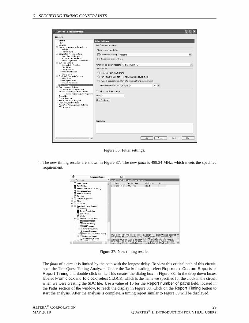
3. From the main Quartus® II window, click Assignments > Settings and then select the categoryFitterSettings which opens the window in Figure 36. Three different levels of effort can be given. Choose theAuto Fit option, which instructs the Fitter to stop as soon asit finds an adequate implementation. The FastFit option reduces the compilation time, but it may produce alower fmax. The third option, Standard Fit,forces the Fitter to produce the best implementation it can find; at this effort level the Fitter will exceed theuser’s timing requirements as much as it can, which often results in longer compilation time. ClickOK, andrecompile the circuit.
ALTERA® CORPORATION
MAY 201028
QUARTUS® II I NTRODUCTION FORVHDL U SERS
6 SPECIFYING TIMING CONSTRAINTS
Figure 36: Fitter settings.
4. The new timing results are shown in Figure 37. The newfmax is 489.24 MHz, which meets the specifiedrequirement.
Figure 37: New timing results.
The fmaxof a circuit is limited by the path with the longest delay. To view this critical path of this circuit,open the TimeQuest Timing Analyzer. Under theTasks heading, selectReports > Custom Reports >
Report Timing and double-click on it. This creates the dialog box in Figure38. In the drop down boxeslabeledFrom clock andTo clock, select CLOCK, which is the name we specified for the clock in the circuitwhen we were creating the SDC file. Use a value of 10 for theReport number of paths field, located inthe Paths section of the window, to reach the display in Figure 38. Click on theReport Timing button tostart the analysis. After the analysis is complete, a timingreport similar to Figure 39 will be displayed.
ALTERA® CORPORATION
MAY 201029
QUARTUS® II I NTRODUCTION FORVHDL U SERS
6 SPECIFYING TIMING CONSTRAINTS
Figure 38: Create timing report.
The Report Timing window shows the ten paths with the longest delays in our circuit. We see that thecritical path begins atZreg[9] and ends atOverflow. The first column in the top part of the window showsthe slack for each path, which is the amount of delay that could still beadded to a given path withoutviolating the specified timing constraint. The bottom part of the window shows the actual elements in theselected path and the incremental delay for each stage in thepath.
ALTERA® CORPORATION
MAY 201030
QUARTUS® II I NTRODUCTION FORVHDL U SERS
6 SPECIFYING TIMING CONSTRAINTS
Figure 39: Critical path.
ALTERA® CORPORATION
MAY 201031
QUARTUS® II I NTRODUCTION FORVHDL U SERS
7 QUARTUS® II WINDOWS
7 Quartus® II Windows
The Quartus® II display contains several utility windows which can be positioned in various places on the screen,changed in size, or closed. In Figure 19, which is reproducedin Figure 40, there are five windows.
Figure 40: The main Quartus® II display.
The Project Navigator window is shown near the top left of thefigure. Under the heading Entity, it depicts atree-like structure of the designed circuit using the namesof the entities in the VHDL code of Figure 12.
1. To see the usefulness of this window, open the previously compiled projectquartus_tutorial\addersubtractor.qpfto get a window similar to Figure 40.
2. Double-click on the nameadderkin the hierarchy under the Entity heading. The Quartus® II software willopen the fileaddersubtractor.vhdand highlight the VHDL entity that specifies the adder subcircuit.
3. Right-click on the same name and chooseLocate > Locate in Chip Planner(Floorplan & Chip Editor)from the pop-up menu that appears. This causes the Quartus® II software to display the floorplan, as inFigure 23, and highlight the part that implements the adder subcircuit.
The Tasks window is located below the Project Navigator window in the Quartus® II main window. As youhave already observed, this window displays the compilation progress. It can also be used to edit and start differentstages of the compilation. Double-clicking on a compilation stage from the Tasks window causes that stage of thecompilation to be re-run.
At the bottom of the Quartus® II main window is the Message window, which displays user messages producedduring the compilation process.
The large area in the middle-right of the Quartus® II window is used for various purposes. As we have seen, itis used by Report Viewers and the Text Editor.
A utility window can be moved by dragging its title bar, resized by dragging the window border, or closed byclicking on theX in the top-right corner of that window. A particular utilitywindow can be opened by selecting itfrom theView > Utility Windows menu.
This document is being provided on an “as-is” basis and as an accommodation and therefore all warranties, rep-resentations or guarantees of any kind (whether express, implied or statutory) including, without limitation, war-ranties of merchantability, non-infringement, or fitness for a particular purpose, are specifically disclaimed.