99

RA (AY4398) Modelling of Emissions of SMPSs and SELCs 8273CR2
York EMC Services Ltd. Page 2 of 99 Issue 2
CONTENTS
List of terms and abbreviations.............................................................................................6
Executive summary...............................................................................................................7
1 Introduction...................................................................................................................8
1.1 Literature....................................................................................................................8
2 Components and Component Measurements................................................................9
2.1 Why measure?............................................................................................................9
2.2 Components ...............................................................................................................9
2.2.1 Capacitors ..........................................................................................................9
2.2.2 Inductors .........................................................................................................10
2.2.3 Tranformers and common-mode chokes ........................................................12
2.2.4 Transient suppressors.......................................................................................14
2.2.5 Cables and looms .............................................................................................14
2.2.6 Other parasitic elements...................................................................................14
2.3 Measurement techniques..........................................................................................14
2.3.1 Component bridge............................................................................................14
2.3.2 Network analyser .............................................................................................14
2.4 Determining component model parameters .............................................................16
3 Circuit Measurements ...................................................................................................18
3.1 Why measure?..........................................................................................................18
3.2 Measurements required............................................................................................18
3.2.1 Switching element............................................................................................18
3.2.2 Rectifier diodes ................................................................................................18
3.3 Measurement techniques..........................................................................................18
3.3.1 Voltage measurements .....................................................................................18
4 Component measurement Results.................................................................................19
4.1 Item 7: Rotary dimmer.............................................................................................19
4.1.1 L1 - Series Inductor .........................................................................................19
4.1.2 C1 - 0.22µF Input capacitor.............................................................................20

RA (AY4398) Modelling of Emissions of SMPSs and SELCs 8273CR2
York EMC Services Ltd. Page 3 of 99 Issue 2
4.2 Item 5: Printer Power supply ...................................................................................20
4.2.1 Input Common mode choke.............................................................................20
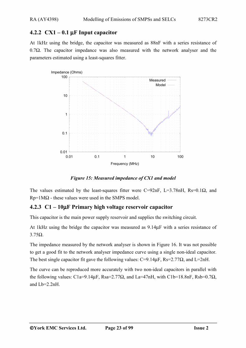
4.2.2 CX1 – 0.1 µF Input capacitor ..........................................................................23
4.2.3 C1 – 10µF Primary high voltage reservoir capacitor.......................................23
4.2.4 C8 – 2.2nF Secondary high voltage reservoir capacitor ..................................24
4.2.5 C2 – 1nF High Voltage Snubber capacitor ......................................................25
4.2.6 Transformer......................................................................................................25
4.2.7 C51 – 1nF Low Voltage Snubber capacitor.....................................................27
4.2.8 C52 – 220µF LV Reservoir capacitor..............................................................27
4.2.9 L Bead – LV Snubber Ferrite Bead (2 used) ...................................................28
4.2.10 LV Common-mode choke...............................................................................28
4.2.11 C11 – 1nF LV negative to HV negative .........................................................29
4.3 Item 6: Plug in power supply...................................................................................30
4.3.1 Input common mode choke..............................................................................30
4.3.2 C1 – 1µF First high voltage reservoir ..............................................................34
4.3.3 C2 – 10µF Second high voltage reservoir .......................................................34
4.3.4 C5 – Snubber capacitor....................................................................................35
4.3.5 C6 – 2.7nF Bridge positive output to low-voltage negative output.................36
4.3.6 Transformer......................................................................................................37
5 SPICE Modelling of Conducted Emissions..................................................................40
5.1 Mains supply model and LISN model .....................................................................40
5.1.1 Derivation of Mains supply model and LISN model.......................................40
5.1.2 Performance of LISN and Mains Supply model..............................................41
5.2 Item 7: Rotary dimmer.............................................................................................42
5.2.1 Mains supply and LISN model ........................................................................42
5.2.2 Triac model ......................................................................................................43
5.2.3 Capacitor models .............................................................................................43
5.2.4 Inductor model .................................................................................................43
5.2.5 Complete dimmer model..................................................................................43
RA (AY4398) Modelling of Emissions of SMPSs and SELCs 8273CR2
York EMC Services Ltd. Page 4 of 99 Issue 2
5.2.6 Analytical Estimate of emissions.....................................................................44
5.2.7 Predicted and measured results........................................................................47
5.3 Item 5: Printer power supply....................................................................................63
5.3.1 Common mode choke ......................................................................................64
5.3.2 Capacitor models .............................................................................................64
5.3.3 Switch transistor and drive circuit model ........................................................64
5.3.4 Transformer model...........................................................................................64
5.3.5 Complete SMPSU model.................................................................................65
5.3.6 Predicted and measured results........................................................................65
5.4 Item 6: Plug in power supply...................................................................................77
5.4.1 Mains supply model and LISN model .............................................................77
5.4.2 Common mode choke ......................................................................................77
5.4.3 Capacitor models .............................................................................................77
5.4.4 Switch transistor and drive circuit model ........................................................77
5.4.5 Transformer model...........................................................................................78
5.4.6 Complete SMPS model....................................................................................78
5.4.7 Predicted and measured results........................................................................78
6 Conclusions...................................................................................................................88
6.1 Component measurements and models....................................................................88
6.2 Waveform measurements.........................................................................................88
6.3 Item 7: Rotary dimmer.............................................................................................88
6.4 Items 5 and 6: Flyback converter power supplies....................................................89
6.5 Modelling harmonic currents in SMPSs/SELCs......................................................89
6.6 Modelling conducted emissions in SMPSs/SELCs .................................................90
6.7 Modelling radiated emissions in SMPSs/SELCs.....................................................90
References.............................................................................................................................91
Appendix 1 Computation of Conducted Emissions..............................................................92
Dolisnpkavdet – the main program......................................................................................92
lisnpkavdet – process the data..............................................................................................93
RA (AY4398) Modelling of Emissions of SMPSs and SELCs 8273CR2
York EMC Services Ltd. Page 5 of 99 Issue 2
ifftextend – compute the conjugate image of a spectrum prior to ifft .................................97
Appendix 2 Phase control waveform generation .................................................................98
Testlisnfft_pc – generate phase control waveforms.............................................................98

RA (AY4398) Modelling of Emissions of SMPSs and SELCs 8273CR2
York EMC Services Ltd. Page 6 of 99 Issue 2
LIST OF TERMS AND ABBREVIATIONS AC Alternating Current
CENELEC Comité Européen de Normalisation Electrotechnique
CISPR Comité International Spécial des Perturbations Radioélectriques
COTS Commercial Off The Shelf
DC Direct Current
DSO Digital Signal Oscilloscope
EMC Electromagnetic Compatibility
EMI Electromagnetic Interference
EUT Equipment Under Test
FET Field Effect Transistor
FFT Fast Fourier Transform
LISN Line Impedance Stabilisation Network
MOSFET Metal-Oxide Semiconductor Field-Effect Transistor
OATS Open Area Test Site
PC Personal Computer
PCB Printed Circuit Board
PWM Pulse Width Modulation
RA Radiocommunications Agency
RF Radio Frequency
RMS Root mean square
RTCG Radio Technology and Compatibility Group
SELCs Switched Electronic Load Controllers
SMPSs Switched Mode Power Supplies
SPICE Simulation Program with Integrated Circuit Emphasis
UKAS United Kingdom Accreditation Service
YES York EMC Services Ltd

RA (AY4398) Modelling of Emissions of SMPSs and SELCs 8273CR2
York EMC Services Ltd. Page 7 of 99 Issue 2
EXECUTIVE SUMMARY The measurement and estimation of component data to allow the modelling of a Switched Electronic Load Controller (SELC) has been described and data presented for a phase controller (dimmer switch) and two low-power Switched-Mode Power Supplies (SMPSs) based on the flyback converter topology.
The operating waveforms of the SMPSs/SELC have been measured and the data used to determine the switching parameters of the models for simulation of harmonic and conducted interference.
Simulations of two SMPSs (items 5 and 6) and one SELC (item7) have been performed, using the PSPICE circuit simulator, at 100% and 50% output power and compared with measurements [1] conducted at a UKAS accredited test laboratory.
The results indicate that the PSPICE models produce an accurate estimate of harmonic currents. In the case of conducted emissions, the PSPICE models predict the structure of the interference spectrum and the changes with load, but overall amplitude accuracy is poor. The accuracy decreases with increasing frequency and this is indicative of the difficulty of determining all of the parasitic elements present in components and their effects on the circuit. In order to consider the prospect of predicting radiated emissions, further work must be carried out to determine the circuit and component data needed to accurately determine the high frequency characteristics of the waveforms. Also, the effect of circuit geometry must be considered.

RA (AY4398) Modelling of Emissions of SMPSs and SELCs 8273CR2
York EMC Services Ltd. Page 8 of 99 Issue 2
1 INTRODUCTION This report describes work carried out to determine the feasibility of modelling conducted emissions (including mains harmonics) from SMPSs/SELC using a SPICE based circuit simulator (PSPICE evaluation version 8 [2] was used to perform all the simulations described in this report). Both switched-mode (flyback) and phase control is considered.
In order to model the EMC performance of a SMPS or SELC, a detailed knowledge of the components used and operation of the circuit is required. The component and circuit measurements undertaken to enable the modelling are also described.
1.1 Literature The following is a short summary of information available in the literature. Very little has been written on the topic of simulation of interference generated by SMPSs/SELCs.
Basso [3] describes the use of approximate SPICE models to predict the differential conducted interference from SMPSs and shows how to get average spectrum results directly from the SPICE simulation. He uses a pulsed current source with the filter components rather than attempting to model the switch and inductor. Basso also suggests the book by Sandler [4] and an article by Bello [5] as useful sources on the simulation of SMPSs.
Hargis [6] describes the use of SPICE modelling to predict the conducted emissions for variable speed (inverter type) motor drives. Again, simplified models of the switching circuit (current or voltage sources) are used.
Kwasniok [7] describes the measurement of power-line impedances in the range from 500kHz to 500MHz, also of the input impedance of mains powered equipment [8].
Tihanyi [9] gives useful advice on design of filters and components in power circuits.
Malack [10] (from Tihanyi) has a number of papers on conducted interference in particular measurement of the power supply impedances across a range of outlets.
Williams [11] gives a good overview of EMC and product design and associated EMC standards.
Vladimirescu [12] explains the operation of the SPICE and PSPICE circuit simulators though it does not replace the software manuals, which are essential reading for the user.

RA (AY4398) Modelling of Emissions of SMPSs and SELCs 8273CR2
York EMC Services Ltd. Page 9 of 99 Issue 2
2 COMPONENTS AND COMPONENT MEASUREMENTS
2.1 Why measure? It is necessary to determine the nominal value of components, which affect the propagation of interference, and also the value of parasitic elements. For inductive components, values are seldom marked. Even where manufacturers data is available, it is often incomplete (e.g. leakage inductance in common-mode chokes). The parasitic capacitance and inductance of devices such as transient suppressors is not always readily available. Capacitors exhibit parasitic inductance and loss mechanisms, which must be considered in any high frequency model.
2.2 Components 2.2.1 Capacitors
An ideal capacitor should have a purely reactive impedance ZC=1/jωC, however stray inductance, resistance and dielectric loss modify this. A good approximation to the actual impedance of a capacitor is:
ZR j C
j L Rc
p
s s=+
+ +1
1ω
ω Equation 1
where ω = 2πf. An equivalent circuit for a typical capacitor is given in Figure 1 below.
Figure 1: An equivalent circuit for a typical capacitor
RA (AY4398) Modelling of Emissions of SMPSs and SELCs 8273CR2
York EMC Services Ltd. Page 10 of 99 Issue 2
0.1kHz 1.0kHz 10kHz 100kHz 1.0MHz 10MHz 100MHz
Frequency
1
0.1
10
100
1000
10 000
0.01
Impedance (Ohms)
a
b
c
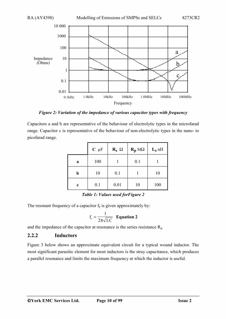
Figure 2: Variation of the impedance of various capacitor types with frequency
Capacitors a and b are representative of the behaviour of electrolytic types in the microfarad range. Capacitor c is representative of the behaviour of non-electrolytic types in the nano- to picofarad range.
C µF Rs Ω Rp MΩ Ls nH
a 100 1 0.1 1
b 10 0.1 1 10
c 0.1 0.01 10 100
Table 1: Values used forFigure 2
The resonant frequency of a capacitor fr is given approximately by:
fLCr =
12π
Equation 2
and the impedance of the capacitor at resonance is the series resistance Rs.
2.2.2 Inductors
Figure 3 below shows an approximate equivalent circuit for a typical wound inductor. The most significant parasitic element for most inductors is the stray capacitance, which produces a parallel resonance and limits the maximum frequency at which the inductor is useful.

RA (AY4398) Modelling of Emissions of SMPSs and SELCs 8273CR2
York EMC Services Ltd. Page 11 of 99 Issue 2
Figure 3: An equivalent circuit for an inductor
The series resistance Rs represents the resistance of the coil, the shunt resistance Rp is an approximate model of core losses and can include the effect of reduced core permeability with increased operating frequency. Cp provides a single lumped model for the turn-to-turn capacitance.
10kHz 100kHz 1.0MHz 10MHz 100MHz
Frequency
1
10
100
1000
10 000
Impedance(Ohms)
a
b
c
Figure 4: Variation of the Impedance of real inductors with frequency
The inductor impedances shown in Figure 4 illustrate the typical behaviour of the model and have the following values:
L µΗ C pF Rp MΩ Rs Ω
a 1 10 10 1
b 10 30 10 10
c 100 100 10 100
Table 2: Values used for Figure 4

RA (AY4398) Modelling of Emissions of SMPSs and SELCs 8273CR2
York EMC Services Ltd. Page 12 of 99 Issue 2
The impedance of the approximate model is given by:
CjRLjR
Z
Sp
L
ωω
++
+=
111 Equation 3
where ω = 2πf. The resonant frequency fr is given approximately by:
fLCr =
12π
Equation 4
The impedance at resonance is approximately equal to Rp if Rs is small.
2.2.3 Tranformers and common-mode chokes
All of the preceding description of inductors applies to transformers and common-mode chokes. However, transformers have additional complexities, which must be considered, for example, leakage reactance and interwinding capacitance. Figure 5 shows an approximate equivalent circuit for a transformer with two windings. In the measurements performed later, it is shown that extra resistances, in series with Cp1 and Cp2 and shunt resistances across the inductor, are sometimes required to improve the model accuracy.
Cm/2
Cm/2
Lm
L1 L2
Rs1 Rs2
Cp1 Cp2
Figure 5: Equivalent circuit of a transformer
The main features of the equivalent circuit are the individual winding parallel capacitances Cp1 and Cp2 and the interwinding (mutual) capacitance Cm shown split into to halves in the diagram; in practice the capacitances are distributed throughout the windings. The mutual

RA (AY4398) Modelling of Emissions of SMPSs and SELCs 8273CR2
York EMC Services Ltd. Page 13 of 99 Issue 2
capacitance of a ‘standard’ (small power type) transformer with two windings on the same bobbin is in the range 10-50pF. This can be reduced by the use of split bobbin arrangements to the region of 5pF. If an interwinding screen (Figure 6) is used, the interwinding capacitance can be reduced to the region of 0.001pF; this small value can be jeopardised if the layout of interconnections is not considered carefully. The winding capacitance of a power transformer is considerably larger than the interwinding capacitance and may be several hundreds of picofarads.
Primary winding
Secondary winding
Guard screen
CORE
Figure 6: Use of interwinding screen
2.2.3.1 Determining the mutual and leakage inductance of common mode chokes With the windings connected in series, anti-phase (ie a common mode choke with a differential mode signal) the inductance measured is the sum of the two leakage inductances:
MLLLSA 221 −+= Equation 5
Where L1 and L2 are the winding self-inductances and M is the mutual inductance between the windings. If the winding inductances are identical ( 21 LLL == ), then the leakage
inductance of each winding is 2LSA . The mutual inductance is related to the winding
inductances by the coupling factor k (this also is used by SPICE to define the mutual inductance between coupled windings):
kLLLkM == 21 Equation 6
If the winding inductances and LSA are known then from Equation 5 and Equation 6:
L
LL
LM
LLMk
SA2
21
−=== Equation 7
From k and L we can determine the leakage inductance

RA (AY4398) Modelling of Emissions of SMPSs and SELCs 8273CR2
York EMC Services Ltd. Page 14 of 99 Issue 2
( )kLLLkLLLSA −=−+= 122 21
21 Equation 8
2.2.3.2 Determining the coupling factor of a transformer With the other windings short circuit the primary inductance is equal to the leakage inductance of the primary plus the effect of the leakage inductance of the primary on the other windings. In the case of two windings:
)1( 21
2
2
1 kLLMLLK −=−=
so that
1
1
LLLk K−
= Equation 9
2.2.4 Transient suppressors
These may have a significant capacitance, so their effect should be considered.
2.2.5 Cables and looms
The effects of cables and looms may be significant – they will have shunt capacitance and series inductance.
2.2.6 Other parasitic elements
Stray inductances and capacitances due to layout will become more significant as frequencies increase.
2.3 Measurement techniques 2.3.1 Component bridge
A component bridge is a simple and accurate method of measuring passive components. However only an impedance value, at a single frequency, is obtained with no indication of the values of parasitic elements. A component bridge typically measures components using an excitation frequency of tens of hertz to few kilohertz – the high frequency behaviour of magnetic cores cannot be determined.
A Prism AIM 6401 LCR databridge was used in this work to obtain component values at 100Hz and/or 1kHz.
2.3.2 Network analyser
A radio frequency network analyser is capable of measuring impedance (reflection) and transmission over a wide frequency range. It is not as accurate as a component bridge particularly when the component impedance is different from the analyser reference impedance (typically 50 ohms). It is also expensive compared to a component bridge.
RA (AY4398) Modelling of Emissions of SMPSs and SELCs 8273CR2
York EMC Services Ltd. Page 15 of 99 Issue 2
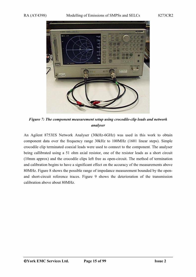
Figure 7: The component measurement setup using crocodile-clip leads and network analyser
An Agilent 8753ES Network Analyser (30kHz-6GHz) was used in this work to obtain component data over the frequency range 30kHz to 100MHz (1601 linear steps). Simple crocodile clip terminated coaxial leads were used to connect to the component. The analyser being callibrated using a 51 ohm axial resistor, one of the resistor leads as a short circuit (10mm approx) and the crocodile clips left free as open-circuit. The method of termination and calibration begins to have a significant effect on the accuracy of the measurements above 80MHz. Figure 8 shows the possible range of impedance measurement bounded by the open- and short-circuit reference traces. Figure 9 shows the deterioration of the transmission calibration above about 80MHz.

RA (AY4398) Modelling of Emissions of SMPSs and SELCs 8273CR2
York EMC Services Ltd. Page 16 of 99 Issue 2
0.01
0.1
1
10
100
1000
10000
100000
1e+006
0 10 20 30 40 50 60 70 80 90 100
|Z| (Ohms)
Frequency (MHz)
Reference loads with croc-clip termination
Open circuit51 Ohm loadShort circuit
Figure 8: Reference load impedances measured using crocodile-clip terminated coaxial cable
0.86
0.88
0.9
0.92
0.94
0.96
0.98
1
1.02
0 10 20 30 40 50 60 70 80 90 100-1
0
1
2
3
4
5
6S21 (Degrees)
Frequency (MHz)
S21 (transmission)f
MagnitudePhase
Figure 9: Reference transmission (S21) measured using crocodile-clip terminated coaxial cable
2.4 Determining component model parameters Measurements from the LCR bridge (Inductance, Capacitance and Resistance bridge) give an equivalent series or parallel circuit for the component measured at a low frequency (100Hz or 1kHz in the case of the bridge used here). This does not provide sufficient information to

RA (AY4398) Modelling of Emissions of SMPSs and SELCs 8273CR2
York EMC Services Ltd. Page 17 of 99 Issue 2
determine the values required for the circuit models described above. If a swept frequency measurement (of impedance) is taken which includes the self-resonant frequency of the component then the model values may be estimated simply from the curve, or by the use of a fitting algorithm. In this work, the gnuplot plotting software [13] is used which incorporates a non-linear least mean squares fitter based on the Marquardt-Levenberg algorithm [14, p683ff]. In practice it was necessary to constrain the range over which the fit was performed to obtain useable results in all cases. Sometimes it was necessary to use several frequency ranges, one for each parameter.
RA (AY4398) Modelling of Emissions of SMPSs and SELCs 8273CR2
York EMC Services Ltd. Page 18 of 99 Issue 2
3 CIRCUIT MEASUREMENTS
3.1 Why measure? Measurements of key currents and voltages in the circuit are necessary for the following reasons:
• Accurate component models for the power semiconductors are likely to be difficult to obtain and may suffer wide variation from component to component. Measurement of the waveforms on a particular supply may be the only way to ensure that the model matches the circuit.
• Validation of the model – any significant variation, in the waveforms, between the model and the real circuit indicates that the model does not contain sufficient detail to reproduce the behaviour of the circuit.
3.2 Measurements required 3.2.1 Switching element
The voltage across the main switching element and the current trough is likely to be critical in determining the EMC performance of the system. The rise time of the waveform will determine the high frequency spectrum of the interference generated. Ringing on the waveform will indicate the resonant frequency of any parasitic elements.
The point of switching in phase controllers is essential to ensure that the model reproduces the overall load waveform. In SMPSs the switching frequency and duty cycle are essential to determine the frequency of emissions and confirm the correct operation of any model.
3.2.2 Rectifier diodes
Where a rectifier is present measurement of the current and/or voltage will indicate whether any reverse current transients occur which may significantly effect the interference levels.
3.3 Measurement techniques 3.3.1 Voltage measurements
A Tektronix TDS2024 200MHz DSO was used to measure and record the circuit waveforms. Tektronix P2200 X10 probes (200MHz) and PMK PHV621 X100 probes were used to measure all voltages to minimise any loading effect. The capacitance of the X10/X100 probes (~25pF) may still affect the measurement (loading the circuit) though their effect is difficult to determine with any precision.
RA (AY4398) Modelling of Emissions of SMPSs and SELCs 8273CR2
York EMC Services Ltd. Page 19 of 99 Issue 2
4 COMPONENT MEASUREMENT RESULTS This section summarises the measurements made on individual components to facilitate modelling of the equipment under tests (EUTs).
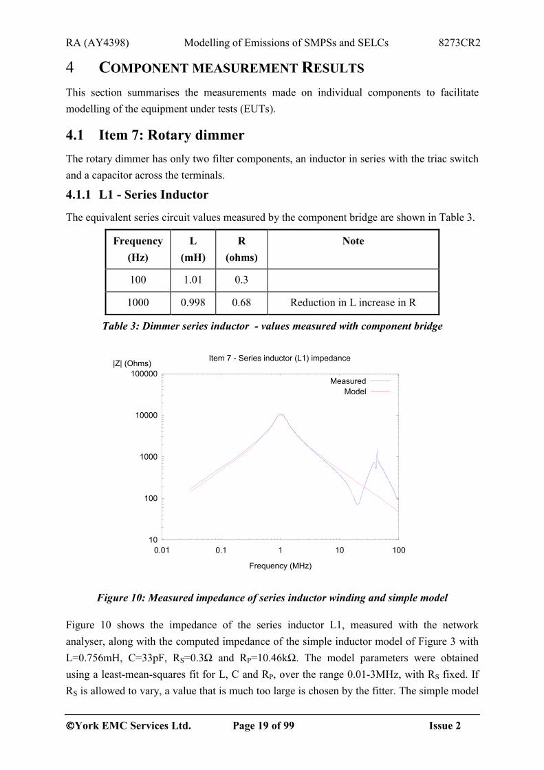
4.1 Item 7: Rotary dimmer The rotary dimmer has only two filter components, an inductor in series with the triac switch and a capacitor across the terminals.
4.1.1 L1 - Series Inductor
The equivalent series circuit values measured by the component bridge are shown in Table 3.
Frequency (Hz)
L (mH)
R (ohms)
Note
100 1.01 0.3
1000 0.998 0.68 Reduction in L increase in R
Table 3: Dimmer series inductor - values measured with component bridge
10
100
1000
10000
100000
0.01 0.1 1 10 100
|Z| (Ohms)
Frequency (MHz)
Item 7 - Series inductor (L1) impedance
MeasuredModel
Figure 10: Measured impedance of series inductor winding and simple model
Figure 10 shows the impedance of the series inductor L1, measured with the network analyser, along with the computed impedance of the simple inductor model of Figure 3 with L=0.756mH, C=33pF, RS=0.3Ω and RP=10.46kΩ. The model parameters were obtained using a least-mean-squares fit for L, C and RP, over the range 0.01-3MHz, with RS fixed. If RS is allowed to vary, a value that is much too large is chosen by the fitter. The simple model
RA (AY4398) Modelling of Emissions of SMPSs and SELCs 8273CR2
York EMC Services Ltd. Page 20 of 99 Issue 2
fit becomes poor above 3MHz and another feature can be seen at around 30MHz, which is similar to that of the common-mode choke of Figure 24. The inductance estimated here is lower than that measured by the bridge. It can also be seen that the impedance of the simple model falls below that of the measurement at the lower end of the frequency range. These two facts imply that the permeability of the core falls with frequency in the range1kHz to 500kHz.
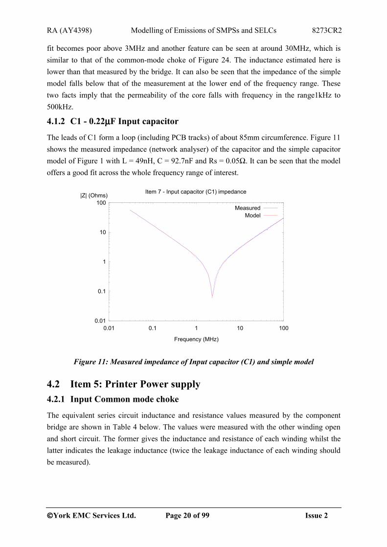
4.1.2 C1 - 0.22µµµµF Input capacitor
The leads of C1 form a loop (including PCB tracks) of about 85mm circumference. Figure 11 shows the measured impedance (network analyser) of the capacitor and the simple capacitor model of Figure 1 with L = 49nH, C = 92.7nF and Rs = 0.05Ω. It can be seen that the model offers a good fit across the whole frequency range of interest.
0.01
0.1
1
10
100
0.01 0.1 1 10 100
|Z| (Ohms)
Frequency (MHz)
Item 7 - Input capacitor (C1) impedance
MeasuredModel
Figure 11: Measured impedance of Input capacitor (C1) and simple model
4.2 Item 5: Printer Power supply 4.2.1 Input Common mode choke
The equivalent series circuit inductance and resistance values measured by the component bridge are shown in Table 4 below. The values were measured with the other winding open and short circuit. The former gives the inductance and resistance of each winding whilst the latter indicates the leakage inductance (twice the leakage inductance of each winding should be measured).

RA (AY4398) Modelling of Emissions of SMPSs and SELCs 8273CR2
York EMC Services Ltd. Page 21 of 99 Issue 2
Winding Frequency (Hz)
L (mH)
R (ohms)
Note
Either 1000 116.2 24 Other winding open
Either 1000 0.99 7.6 Other winding short
Table 4: Common-mode choke - values measured with component bridge
The impedance of one winding with the other open and short respectively were also measured with a network analyser and a least-means square fitter used to estimate the component values. The results are shown in Figure 12. The open circuit reference impedance limit is also shown. It can be seen that the winding impedance is close to the open-circuit measurement limit in the frequency range 0.03-0.5MHz which makes any values obtained by this method suspect. The winding inductance estimated by this method is 58.0mH, compared with the value of 116.2mH measured with the component bridge – the choke is air-cored so such a large change with frequency is not expected.
100
1000
10000
100000
1e+006
0.01 0.1 1 10 100
Impedance (Ohms)
Frequency (MHz)
Other winding open circuitOther winding short circuit
PSPICE Other winding open circuitPSPICE Other winding short circuit
Open circuit reference
Figure 12: Measured impedance of Input common-mode choke and PSPICE model
The common-mode and differential mode transmission coefficients (S21) were also measured with the network analyser and the component values estimated using the least-mean squares fitter. The results are shown in Figure 14.
In order to match the impedance the choke equivalent circuit of Figure 5 was modified as shown in Figure 13 with additional resistances series in series with the winding capacitances.

RA (AY4398) Modelling of Emissions of SMPSs and SELCs 8273CR2
York EMC Services Ltd. Page 22 of 99 Issue 2
The frequency of the feature at about 2MHz depends on the coupling factor and its Q-factor depends on the additional loss elements RS1b and RS2b.
Figure 13: Improved PSPICE model for common-mode choke – values as for Figure 25.
The estimated parameters for the choke model are: L=117.8mH(winding impedance), Cp=2.56pF (winding capacitance) Rs=4.5Ω (winding series resistance), Rp=364kΩ, Rsb=400Ω (resistor in series with Cp), Lk=453.5µH, Cm=4.77pF (inter-winding capacitance). These parameters are used in the simulation results presented below.
0.0001
0.001
0.01
0.1
1
0.01 0.1 1 10 100
S21
Frequency (MHz)
Measured: Differential ModePSPICE: Differential ModeMeasured: Common Mode
PSPICE: Common Mode
Figure 14: Measured S21 of Input common-mode choke and PSPICE model in differential- and common-mode
RA (AY4398) Modelling of Emissions of SMPSs and SELCs 8273CR2
York EMC Services Ltd. Page 23 of 99 Issue 2
4.2.2 CX1 – 0.1 µµµµF Input capacitor
At 1kHz using the bridge, the capacitor was measured as 88nF with a series resistance of 0.7Ω. The capacitor impedance was also measured with the network analyser and the parameters estimated using a least-squares fitter.
0.01
0.1
1
10
100
0.01 0.1 1 10 100
Impedance (Ohms)
Frequency (MHz)
MeasuredModel
Figure 15: Measured impedance of CX1 and model
The values estimated by the least-squares fitter were C=92nF, L=3.78nH, Rs=0.1Ω, and Rp=1MΩ - these values were used in the SMPS model.
4.2.3 C1 – 10µµµµF Primary high voltage reservoir capacitor
This capacitor is the main power supply reservoir and supplies the switching circuit.
At 1kHz using the bridge the capacitor was measured as 9.14µF with a series resistance of 3.75Ω.
The impedance measured by the network analyser is shown in Figure 16. It was not possible to get a good fit to the network analyser impedance curve using a single non-ideal capacitor. The best single capacitor fit gave the following values: C=9.14µF, Rs=2.77Ω, and L=2nH.
The curve can be reproduced more accurately with two non-ideal capacitors in parallel with the following values: C1a=9.14µF, Rsa=2.77Ω, and La=47nH, with C1b=18.8nF, Rsb=0.7Ω, and Lb=2.2nH.

RA (AY4398) Modelling of Emissions of SMPSs and SELCs 8273CR2
York EMC Services Ltd. Page 24 of 99 Issue 2
0.01
0.1
1
10
100
1000
0.01 0.1 1 10 100
Impedance (Ohms)
Frequency (MHz)
MeasuredSingle capacitor fit
C1aC1b
Two capacitor fit
Figure 16: Measured impedance of C1 and models
4.2.4 C8 – 2.2nF Secondary high voltage reservoir capacitor
This capacitor supplies only the control IC.
At 1kHz using the bridge the capacitor was measured as 2.28nF with a series resistance of 980Ω - this is not a reasonable resistance value and has been ignored. With the network analyser the best fit gave: C=2.28nF, Rs=2.0Ω, and L=1.8nH.
1
10
100
1000
10000
0.01 0.1 1 10 100
Impedance (Ohms)
Frequency (MHz)
MeasuredModel
Figure 17: Measured impedance of C8 and model

RA (AY4398) Modelling of Emissions of SMPSs and SELCs 8273CR2
York EMC Services Ltd. Page 25 of 99 Issue 2
4.2.5 C2 – 1nF High Voltage Snubber capacitor
The bridge measurement gave a value of C=1.046nF Rs=2.2kOhms at 1kHz. The network analyser best fit gave: C=1.05nf, Rs=0.4Ω, and L=1.53nH. Note that there appears to be an additional feature in the measured data near resonance, which is not reproduced by the simple model.
0.1
1
10
100
1000
10000
0.01 0.1 1 10 100
Impedance (Ohms)
Frequency (MHz)
MeasuredModel
Figure 18: Measured impedance of C2 and model
4.2.6 Transformer
In analysing the SMPS, the transformer primary is of great importance as it affects the shape of the switching waveform.
Winding Frequency (Hz)
L (mH)
R (ohms)
Note
Primary (L1) 1000 1.17 1 All other windings open
Switch power (L2) 1000 0.282 0.458 “
LV Secondary (L3) 1000 0.1675 0.115 “
Primary (L1) 1000 0.0013 1.68 All other windings shorted (leakage inductance)
Table 5: Transformer – inductance values measured with component bridge
RA (AY4398) Modelling of Emissions of SMPSs and SELCs 8273CR2
York EMC Services Ltd. Page 26 of 99 Issue 2
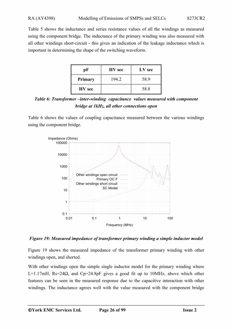
Table 5 shows the inductance and series resistance values of all the windings as measured using the component bridge. The inductance of the primary winding was also measured with all other windings short-circuit - this gives an indication of the leakage inductance which is important in determining the shape of the switching waveform.
pF HV sec LV sec
Primary 194.2 58.9
HV sec 58.8
Table 6: Transformer –inter-winding capacitance values measured with component bridge at 1kHz, all other connections open
Table 6 shows the values of coupling capacitance measured between the various windings using the component bridge.
0.1
1
10
100
1000
10000
100000
0.01 0.1 1 10 100
Impedance (Ohms)
Frequency (MHz)
Other windings open circuitPrimary OC F
Other windings short circuitSC Model
Figure 19: Measured impedance of transformer primary winding a simple inductor model
Figure 19 shows the measured impedance of the transformer primary winding with other windings open, and shorted.
With other windings open the simple single inductor model for the primary winding where L=1.17mH, Rs=24Ω, and Cp=24.8pF gives a good fit up to 10MHz, above which other features can be seen in the measured response due to the capacitive interaction with other windings. The inductance agrees well with the value measured with the component bridge

RA (AY4398) Modelling of Emissions of SMPSs and SELCs 8273CR2
York EMC Services Ltd. Page 27 of 99 Issue 2
indicating that the core permeability remains constant from 1 kHz up to at least the winding resonance.
With other windings shorted the simple single inductor model for the primary winding where L=0.8µH, Rs=1.06Ω, and Cp=102pF was the best fit obtainable – it does not reproduce the resonant peak well or other features above 10MHz.
In the PSPICE model, only the primary and a single secondary were modelled using the values shown on the circuit diagram.
4.2.7 C51 – 1nF Low Voltage Snubber capacitor
It was not possible to remove this chip capacitor from the PCB. An ideal capacitor of 1nF is used in the simulation.
4.2.8 C52 – 220µµµµF LV Reservoir capacitor
The bridge measurement gave the following values for C52: C=210µF, Rs=0.085Ω, at 1kHz. The impedance curve for these values with a series inductance of 48nH is shown in Figure 20 as “C52a”.
The impedance curve measured with the network analyser (Figure 20) gave a single capacitor fit with: C=12µF, Rs=0.085Ω, and L=7nH – shown as “C52b”. Clearly there is a considerable discrepancy between the two sets of values. In order to satisfy both measurements, both capacitors were used in parallel in the model, the large capacitor dominates the impedance value at low frequencies and the small capacitor dominates the impedance value at high frequencies.
0.01
0.1
1
10
100
0.001 0.01 0.1 1 10 100
Impe
danc
e (O
hms)
Frequency (MHz)
MeasuredC52aC52b
Two capacitor fit
Figure 20: Measured impedance of C52 and model
RA (AY4398) Modelling of Emissions of SMPSs and SELCs 8273CR2
York EMC Services Ltd. Page 28 of 99 Issue 2
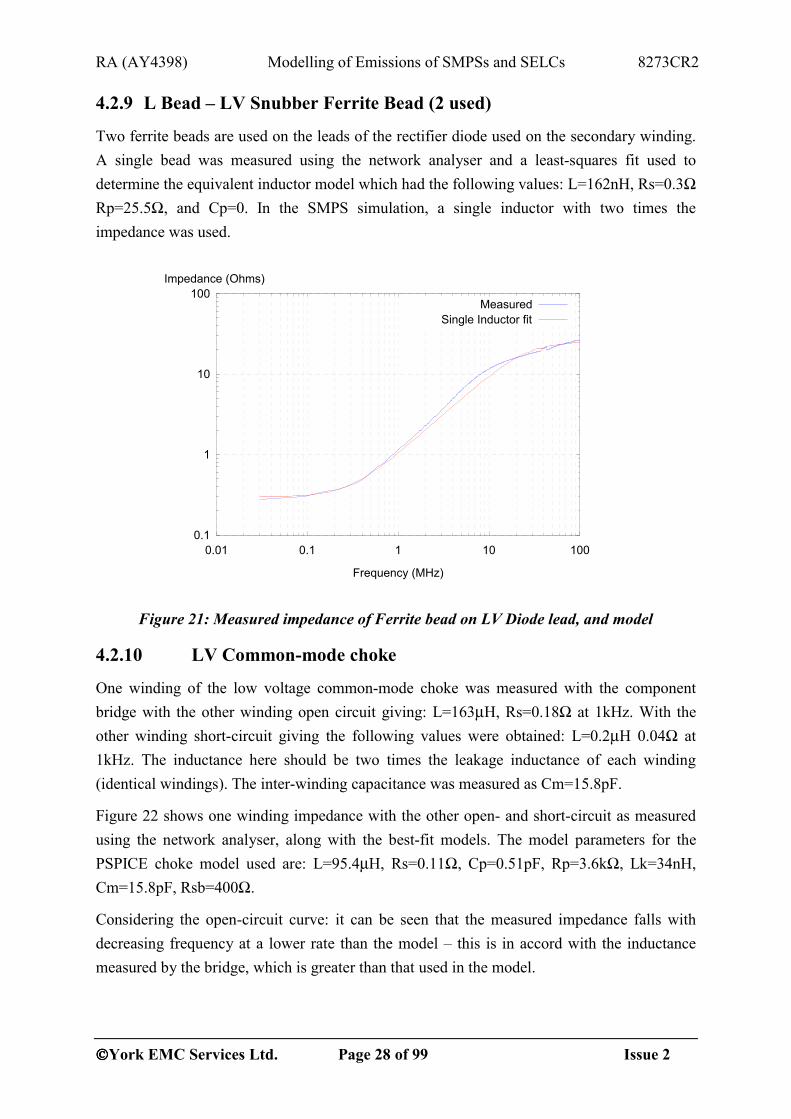
4.2.9 L Bead – LV Snubber Ferrite Bead (2 used)
Two ferrite beads are used on the leads of the rectifier diode used on the secondary winding. A single bead was measured using the network analyser and a least-squares fit used to determine the equivalent inductor model which had the following values: L=162nH, Rs=0.3Ω Rp=25.5Ω, and Cp=0. In the SMPS simulation, a single inductor with two times the impedance was used.
0.1
1
10
100
0.01 0.1 1 10 100
Impedance (Ohms)
Frequency (MHz)
MeasuredSingle Inductor fit
Figure 21: Measured impedance of Ferrite bead on LV Diode lead, and model
4.2.10 LV Common-mode choke
One winding of the low voltage common-mode choke was measured with the component bridge with the other winding open circuit giving: L=163µH, Rs=0.18Ω at 1kHz. With the other winding short-circuit giving the following values were obtained: L=0.2µH 0.04Ω at 1kHz. The inductance here should be two times the leakage inductance of each winding (identical windings). The inter-winding capacitance was measured as Cm=15.8pF.
Figure 22 shows one winding impedance with the other open- and short-circuit as measured using the network analyser, along with the best-fit models. The model parameters for the PSPICE choke model used are: L=95.4µH, Rs=0.11Ω, Cp=0.51pF, Rp=3.6kΩ, Lk=34nH, Cm=15.8pF, Rsb=400Ω.
Considering the open-circuit curve: it can be seen that the measured impedance falls with decreasing frequency at a lower rate than the model – this is in accord with the inductance measured by the bridge, which is greater than that used in the model.

RA (AY4398) Modelling of Emissions of SMPSs and SELCs 8273CR2
York EMC Services Ltd. Page 29 of 99 Issue 2
0.1
1
10
100
1000
10000
100000
1e+006
0.01 0.1 1 10 100
Impedance (Ohms)
Frequency (MHz)
Other winding open circuitOther winding short circuit
PSPICE Other winding open circuitPSPICE Other winding short circuit
Open circuit reference
Figure 22: Measured impedance of output common-mode choke and PSPICE model – note the feature at around 30MHz which corresponds to the feature in the open-circuit
reference trace
4.2.11 C11 – 1nF LV negative to HV negative
The bridge gave a value of 960pF at 1kHz for this capacitor, the series resistance was not recorded. The network analyser measurement gives a best-fit model with C=960pF, Rs=0.3Ω, and L=16nH.
0.1
1
10
100
1000
10000
100000
0.01 0.1 1 10 100
Impedance (Ohms)
Frequency (MHz)
MeasuredModel
Figure 23: Measured impedance of C11 and model
RA (AY4398) Modelling of Emissions of SMPSs and SELCs 8273CR2
York EMC Services Ltd. Page 30 of 99 Issue 2
4.3 Item 6: Plug in power supply 4.3.1 Input common mode choke
The equivalent series circuit inductance and resistance values measured by the component bridge are shown in Table 7:
Winding Frequency (Hz)
L (mH)
R (ohms)
Note
Wide pin gap 100 8.7 4.4
1000 29.3 35 Significant difference from 100Hz
Narrow gap pins 100 8.73 4.45
1000 29.3 34.5 Significant difference from 100Hz
Parallel (common-mode)
100 7.95 2.26
1000 28.9 32 Significant difference from 100Hz
Series (differential
mode)
100 0.093 8.82
1000 0.0895 8.88 Significant difference from 100Hz
Table 7: Common-mode choke - values measured with component bridge
It can be seen from the table that there is a considerable difference in measured inductance at the two bridge frequencies. The reason for this is not known.
The inter-winding capacitance was measured, as 2.2pF, by the component bridge (independent of frequency).
Figure 24 shows the measured impedance of a single winding of the common mode choke (with the other open circuit). The open circuit reference plot is included, along with the computed impedance of the simple inductor model of Figure 3 with L=35mH, C=0.10pF RS=4.45Ω and RP=150kΩ. It can be seen that the peak value of the winding impedance comes close to the measurement limit as illustrated by open circuit plot. The simple model fit becomes poor above 3MHz and another feature can be seen – this is likely to be due to coupling to the second winding. The inductance estimated here is higher than that measured by the bridge.

RA (AY4398) Modelling of Emissions of SMPSs and SELCs 8273CR2
York EMC Services Ltd. Page 31 of 99 Issue 2
100
1000
10000
100000
1e+006
0.01 0.1 1 10 100
|Z| (Ohms)
Frequency (MHz)
Item 6 - Common mode choke (L1) impedance
MeasurementModel
Open circuit
Figure 24: Measured impedance of common mode choke winding (2 measurements) with impedance of simple inductor model, and open circuit
Further investigation demonstrated that the choke winding impedance was due to interaction of the measured and open circuit winding (Figure 24). In order to match the impedance the choke equivalent circuit of Figure 5 was modified as shown in Figure 13 with additional resistance in series with the winding capacitances. The frequency of the feature at 10MHz depends on the coupling factor and its Q-factor depends on the additional loss elements RS1b and RS2b (Figure 13).
RA (AY4398) Modelling of Emissions of SMPSs and SELCs 8273CR2
York EMC Services Ltd. Page 32 of 99 Issue 2
100
1000
10000
100000
1e+006
0.01 0.1 1 10 100
|Z| (Ohms)
Frequency (MHz)
Item 6 - Common mode choke (L1) impedance
Measurement 1PSPICE model
Figure 25: Measured impedance of common mode choke winding and PSPICE model of Figure 13
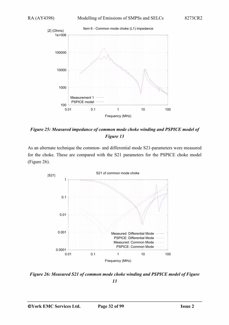
As an alternate technique the common- and differential mode S21-parameters were measured for the choke. These are compared with the S21 parameters for the PSPICE choke model (Figure 26).
0.0001
0.001
0.01
0.1
1
0.01 0.1 1 10 100
|S21|
Frequency (MHz)
S21 of common mode choke
Measured: Differential ModePSPICE: Differential ModeMeasured: Common Mode
PSPICE: Common Mode
Figure 26: Measured S21 of common mode choke winding and PSPICE model of Figure 13

RA (AY4398) Modelling of Emissions of SMPSs and SELCs 8273CR2
York EMC Services Ltd. Page 33 of 99 Issue 2
The parameters of the PSPICE model were adjusted with the aid of a least-mean squares fitter to obtain a better match to the S21 measurements (Figure 27) however this makes the impedance of the winding fit the measurement less well (Figure 28).
0.0001
0.001
0.01
0.1
1
0.01 0.1 1 10 100
|S21|
Frequency (MHz)
S21 of common mode choke
Measured: Differential ModePSPICE: Differential ModeMeasured: Common Mode
PSPICE: Common Mode
Figure 27: Measured S21 of common mode choke winding and PSPICE model of Figure 13 with parameters optimised to fit S21 measurements
100
1000
10000
100000
1e+006
0.01 0.1 1 10 100
|Z| (Ohms)
Frequency (MHz)
Item 6 - Common mode choke (L1) impedance
Measurement 1PSPICE model
Figure 28: Measured impedance of common mode choke winding and PSPICE model of Figure 13 with parameters optimised to fit S21 measurements
RA (AY4398) Modelling of Emissions of SMPSs and SELCs 8273CR2
York EMC Services Ltd. Page 34 of 99 Issue 2
In the SMPS simulations, the circuit of Figure 13 was used.
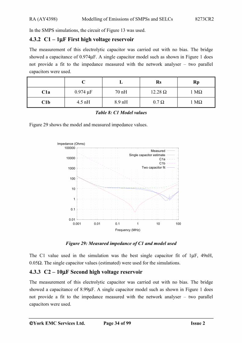
4.3.2 C1 – 1µµµµF First high voltage reservoir
The measurement of this electrolytic capacitor was carried out with no bias. The bridge showed a capacitance of 0.974µF. A single capacitor model such as shown in Figure 1 does not provide a fit to the impedance measured with the network analyser – two parallel capacitors were used.
C L Rs Rp
C1a 0.974 µF 70 nH 12.28 Ω 1 MΩ
C1b 4.5 nH 8.9 nH 0.7 Ω 1 MΩ
Table 8: C1 Model values
Figure 29 shows the model and measured impedance values.
0.01
0.1
1
10
100
1000
10000
100000
0.001 0.01 0.1 1 10 100
Impedance (Ohms)
Frequency (MHz)
MeasuredSingle capacitor estimate
C1aC1b
Two capacitor fit
Figure 29: Measured impedance of C1 and model used
The C1 value used in the simulation was the best single capacitor fit of 1µF, 49nH, 0.05Ω. Τhe single capacitor values (estimated) were used for the simulations.
4.3.3 C2 – 10µµµµF Second high voltage reservoir
The measurement of this electrolytic capacitor was carried out with no bias. The bridge showed a capacitance of 8.99µF. A single capacitor model such as shown in Figure 1 does not provide a fit to the impedance measured with the network analyser – two parallel capacitors were used.

RA (AY4398) Modelling of Emissions of SMPSs and SELCs 8273CR2
York EMC Services Ltd. Page 35 of 99 Issue 2
C L Rs Rp
C2a 8.99 µF 77,8 nH 2.35 Ω 10 MΩ
C2b 34.4 µF 19.6 nH 0.7 Ω 10 MΩ
Table 9: C2 Model values
0.1
1
10
100
1000
10000
0.001 0.01 0.1 1 10 100
Impedance (Ohms)
Frequency (MHz)
MeasuredSingle capacitor fit
C2aC2b
Two capacitor fit
Figure 30: Measured impedance of C2 and model used
4.3.4 C5 – Snubber capacitor
This surface mount capacitor was measured only with the network analyser and the values obtained by fitting the impedance curve were:
C L Rs Rp
2.5 nF 10 nH 5 Ω 10 MΩ
Table 10: C5 Model values

RA (AY4398) Modelling of Emissions of SMPSs and SELCs 8273CR2
York EMC Services Ltd. Page 36 of 99 Issue 2
1
10
100
1000
10000
0.01 0.1 1 10 100
Impedance (Ohms)
Frequency (MHz)
MeasuredFit
Figure 31: Measured impedance of C5 and model used
4.3.5 C6 – 2.7nF Bridge positive output to low-voltage negative output
0.1
1
10
100
1000
10000
0.01 0.1 1 10 100
Impedance (Ohms)
Frequency (MHz)
MeasuredFit
Figure 32: Measured impedance of C6 and model used
This surface mount capacitor was measured as 2.65nF with the bridge. It can be seen in Figure 32 that the model and measurement diverge at the upper frequency limit.

RA (AY4398) Modelling of Emissions of SMPSs and SELCs 8273CR2
York EMC Services Ltd. Page 37 of 99 Issue 2
The values obtained by fitting to the impedance curve measured with the network analyser were:
C L Rs Rp
2.65 nF 1.3 nH 1.8 Ω 1 MΩ
Table 11: C5 Model values
4.3.6 Transformer
In analysing the SMPS, the inductance and self-capacitance of the transformer primary are of great importance as they affect the shape of the switching waveform.
Table 12 shows the inductance and series resistance values of all the windings as measured using the component bridge. The inductance of the primary winding was also measured with all other windings short-circuit – this gives an indication of the leakage inductance which is important in determining the shape of the switching waveform.
Winding Frequency (Hz)
L (mH)
R (ohms)
Note
Primary (L1) 100 2.87 5.7 All other windings open
1000 2.87 5.75 “
Switch power (L2) 100 0.0193 0.45 “
1000 0.0196 0.45 “
LV Secondary (L3) 1000 0.0741 0.531 “
LV Secondary (L4) 1000 0.074 0.54 “
LV Secondary (L5) 1000 0.0118 0.43 “
Primary (L1) 1000 0.0012 0.49 All other windings shorted (leakage inductance)
Table 12: Transformer – inductance values measured with component bridge
Table 13 shows the values of coupling capacitance measured between the various windings using the component bridge.
RA (AY4398) Modelling of Emissions of SMPSs and SELCs 8273CR2
York EMC Services Ltd. Page 38 of 99 Issue 2
pF L1 L2 L3 L4 L5
L1 - 26 11.3 15.8 16.6
L2 - - 29.7 29 16.6
L3 - - - 27.5 16.6
L4 - - - - 31
Table 13: Transformer – capacitance values measured with component bridge at 1kHz, all other connections open
10
100
1000
10000
100000
0.01 0.1 1 10 100
|Z| (Ohms)
Frequency (MHz)
Item 6 - Transformer Primary (L1) impedance
MeasuredModel
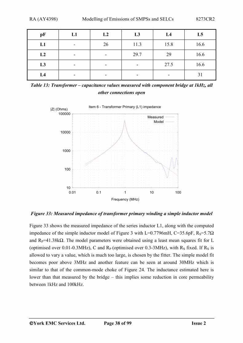
Figure 33: Measured impedance of transformer primary winding a simple inductor model
Figure 33 shows the measured impedance of the series inductor L1, along with the computed impedance of the simple inductor model of Figure 3 with L=0.7796mH, C=35.6pF, RS=5.7Ω and RP=41.38kΩ. The model parameters were obtained using a least mean squares fit for L (optimised over 0.01-0.3MHz), C and RP (optimised over 0.3-3MHz), with RS fixed. If RS is allowed to vary a value, which is much too large, is chosen by the fitter. The simple model fit becomes poor above 3MHz and another feature can be seen at around 30MHz which is similar to that of the common-mode choke of Figure 24. The inductance estimated here is lower than that measured by the bridge – this implies some reduction in core permeability between 1kHz and 100kHz.

RA (AY4398) Modelling of Emissions of SMPSs and SELCs 8273CR2
York EMC Services Ltd. Page 39 of 99 Issue 2
10
100
1000
10000
100000
0.01 0.1 1 10 100
|Z| (Ohms)
Frequency (MHz)
Item 6 - Transformer Primary (L1) impedance
MeasuredModel
Figure 34: Measured impedance of transformer primary winding and improved inductor model
Figure 34 shows the improved low-frequency matched obtained by adding an additional inductor (L2=2.87mH) and parallel resistor (RP2=83.3Ω) which act only at low frequencies. This is a reasonable physical model for the reduction in permeability of a magnetic core with increasing frequency.
The final PSPICE model used a single 2.87mH primary with a 36.5 pF parallel capacitance and 41kΩ parallel resistor – the series resistance was small compared with other elements in the circuit and was not included. A single 74µH secondary winding was used with a coupling factor of 0.99979 (giving a primary leakage inductance of 0.6µH) and a mutual capacitance of 26pF which corresponds to the value measured using the component bridge between the primary and principal secondary windings.
RA (AY4398) Modelling of Emissions of SMPSs and SELCs 8273CR2
York EMC Services Ltd. Page 40 of 99 Issue 2
5 SPICE MODELLING OF CONDUCTED EMISSIONS
5.1 Mains supply model and LISN model 5.1.1 Derivation of Mains supply model and LISN model
In order to replicate the test conditions a PSPICE model of the mains supply network and LISN were constructed. The mains supply is assumed to have the average impedance measured by Malack and J R Engstrom in reference [10]. The LISN is based on the CISPR 16 reference circuit described by Williams [11 p71]. Both are shown in Figure 35 – note that the voltage source is connected to ground at one end as Malack and J R Engstrom describe an equal impedance to ground for Live and Neutral conductors.
Ideal components are used throughout the LISN – no parasitic effects are taken into account. In a well-designed LISN, the component parasitic effects should only be significant outside the measurement frequency band – this assumption has not been tested.
The mains impedance and LISN were implemented as a sub-circuit library model as they are common to the majority of circuits simulated.
The conducted interference waveforms are measured at the nodes Lmeas and Nmeas, across the 50Ω resistors (R3 and R4), which represent the input impedance of the measuring instrument. The harmonic current was determined by monitoring the current supply by the LISN Lout node to the EUT – the effect of the LISN on harmonic measurements should be small.

RA (AY4398) Modelling of Emissions of SMPSs and SELCs 8273CR2
York EMC Services Ltd. Page 41 of 99 Issue 2
Figure 35: Mains Supply and LISN Model showing connection to supply voltage source and EUT
5.1.2 Performance of LISN and Mains Supply model
0.1
1
10
100
0.0001 0.001 0.01 0.1 1 10
Impedance (Ohms)
Frequency (MHz)
Impedance of LISN as seen from EUT
Live to NeutralLive to Earth and Neutral to Earth
Figure 36: Impedance of PSPICE LISN (and mains supply) as seen from EUT

RA (AY4398) Modelling of Emissions of SMPSs and SELCs 8273CR2
York EMC Services Ltd. Page 42 of 99 Issue 2
-4.5
-4
-3.5
-3
-2.5
-2
-1.5
-1
-0.5
0
0.5
0.01 0.1 1 10 100
Transmission (dB)
Frequency (MHz)
Transmission EUT to measuring device - current excitation
Transmission
Figure 37: Transmission from EUT to measuring device for PSPICE LISN
5.2 Item 7: Rotary dimmer
2332/SCH/04 d
230Vac 250W Domestic Light Dimmer
A
1 1Tuesday, January 28, 2003
Title
Size Document Number Rev
Date: Sheet of
PAD1
1
PAD2
1
S?SW SPST
12
C1100nF
12
R?2M
21
R?1M2
13
2
C?47nF
12
D1
DB3
1 2
L1INDUCTOR
12
Q?SCR?3
12
F?
THERMAL FUSE ?
1 2
Figure 38: Dimmer circuit diagram (Item 7)
5.2.1 Mains supply and LISN model
The mains supply and LISN model as described above was used in all simulations of the dimmer circuit.

RA (AY4398) Modelling of Emissions of SMPSs and SELCs 8273CR2
York EMC Services Ltd. Page 43 of 99 Issue 2
5.2.2 Triac model
In order to allow the triac to be precisely controlled, a model was constructed using an ideal switch and PSPICE behavioural modelling capabilities. No generic SPICE model is available for triacs but a number of manufacturers do supply macro-models such as that described by Petrie [15].
The model is triggered by a pulsed voltage source.
5.2.3 Capacitor models
The capacitor model of Figure 1 was implemented as a library element and used to represent the capacitor.
5.2.4 Inductor model
The inductor model of Figure 3 was implemented as a library element and used to represent the series inductor.
5.2.5 Complete dimmer model
Figure 39: Dimmer model for conducted interference with LISN and mains supply incorporated

RA (AY4398) Modelling of Emissions of SMPSs and SELCs 8273CR2
York EMC Services Ltd. Page 44 of 99 Issue 2
5.2.6 Analytical Estimate of emissions
5.2.6.1 Harmonic Spectrum It is possible to estimate the harmonic and conducted spectra from an ideal phase controlled dimmer by treating the current waveform as a 50 Hz sinusoid multiplied by a rectangular pulse train:
( )tItpti lωsinˆ)()( 0= Equation 10
Where lω is the line (mains) frequency, I is the peak value of the sinusoid, and:
Φ≥Φ≤
=πωπω
modmod
10
)(0 tt
tpl
l Equation 11
where Φ is the phase angle (in radians) at which the phase controller begins to conduct.
-2
-1.5
-1
-0.5
0
0.5
1
1.5
2
0 5 10 15 20 25 30
Amplitude
Time (ms)
Pulse train: p_0(t)Current waveform: i(t) (A)
T
Φ−= πτωτ
l
Φ=tlω
∆ 2τ
Figure 40: Current waveform and generating pulse-train
The properties of Fourier transforms can be used to determine the spectrum of product from the individual spectra.

RA (AY4398) Modelling of Emissions of SMPSs and SELCs 8273CR2
York EMC Services Ltd. Page 45 of 99 Issue 2
Starting with the Fourier Series for the periodic unit pulse train delayed by ∆ from t=0 we get:
( ) ( ) ( )∆−
=−= ∫
−
nn
nn jT
dttjtpT
CT
T
ωτωτω exp2
sincexp1 2
2
0 Equation 12
where Cn is the complex amplitude of nth harmonic, ωn is the angular frequency of nth harmonic, T is the period of the pulse train and τ is the pulse width. The pulse train can be reconstructed as
tj
nn
neCp ω∑∞
−∞=
=0 Equation 13
The harmonics of the pulse train are spaced at 100Hz intervals as two pulses must occur per cycle of the 50Hz line frequency. Note also that the position of the constant T differs from that found in some texts – in this form the amplitude of 2Cn (positive and negative frequency harmonics) corresponds to the peak value of the harmonic current which may be divided by
2 to yield the rms value (C0 is directly equal to the current component).
When a waveform is multiplied by a sinusoid of angular frequency ωl the modulation property of the Fourier transform produces the result:
( ) ( ) ( ) ( )[ ]lll FFIjtItf ωωωωω −−+↔ ˆ2
sinˆ Equation 14
The spectrum of the ideal phase controller waveform must therefore consist of harmonics of 100Hz, shifted ±50Hz due to multiplication by the line frequency sine-wave. This results in spectral lines at ±50Hz due to the component, 50 and 150Hz from the first (100Hz) harmonic of the pulse-train, 150 and 250Hz from the second (200Hz) harmonic of the pulse train and so on. We can write the new harmonic spectrum as:
( ) ( )
∆−
−∆−
= +
++ 1
1 exp2
sincexp2
sinc22
1 nn
nn
n jjjC ωτωωτωτ Equation 15
where 2
1+nC is the complex amplitude coefficient of the harmonic at
( ) ( )212002
122
1 +=+=+
nnlnπωω Equation 16
If the pulse train is trapezoidal with a rise/fall time rτ to approximate a finite switching time
the spectrum is modified thus:
( ) ( )
∆−
−
∆−
= +
++ 2
sincexp2
sinc2
sincexp2
sinc2 1
12
1rn
nnrn
nn
n jjjC τωωτωτωωτωτ
Equation 17 The rise and fall time has little effect on the harmonic spectrum if it is small compared with the on-time (pulse width). The analytical result is presented below along with the measured and computed harmonic data.

RA (AY4398) Modelling of Emissions of SMPSs and SELCs 8273CR2
York EMC Services Ltd. Page 46 of 99 Issue 2
5.2.6.2 Conducted Emissions In the case of conducted emissions, analysis is not practical due to the need to replicate the peak and average detection processes in the receiver. Instead an Octave/Matlab [16,17] program was written to generate idealised LISN output waveforms (A sine wave modulated by a trapezoidal pulse) which can be processed by the same software as the PSPICE output. In the case of average detection (but not peak detection), any phase shift due to the filter components will not affect the value of the average. These effects can therefore be computed by post processing the average spectrum.
The LC filter in the LISN can be solved by circuit analysis or using PSPICE (Figure 41).
The LISN circuit is a little more complex and there will be some interaction between the LISN and the filter components, however it can be approximated by a first order high-pass filter with a 100kHz cut-off frequency.
-120
-100
-80
-60
-40
-20
0
20
0.01 0.1 1 10 100
Gain (dB)
Frequency (MHz)
Filter (Analytic)Filter (PSPICE)LISN (Analytic)LISN (PSPICE)
Ideal Filter
Figure 41: Effect of the filter and LISN on propagation of conducted interference – the gain of a filter with ideal components is also shown
The spectrum of an ideal LISN waveform can be multiplied by the transfer functions of the filter components, and LISN to give an approximate solution to the average conducted emissions. This semi-analytical result is presented below along with the measured and computed conducted emissions data.

RA (AY4398) Modelling of Emissions of SMPSs and SELCs 8273CR2
York EMC Services Ltd. Page 47 of 99 Issue 2
Figure 42: Circuit used to determine the Filter and LISN frequency responses
Figure 43: Circuits used to determine the filter frequency response with an ideal representation of the LISN
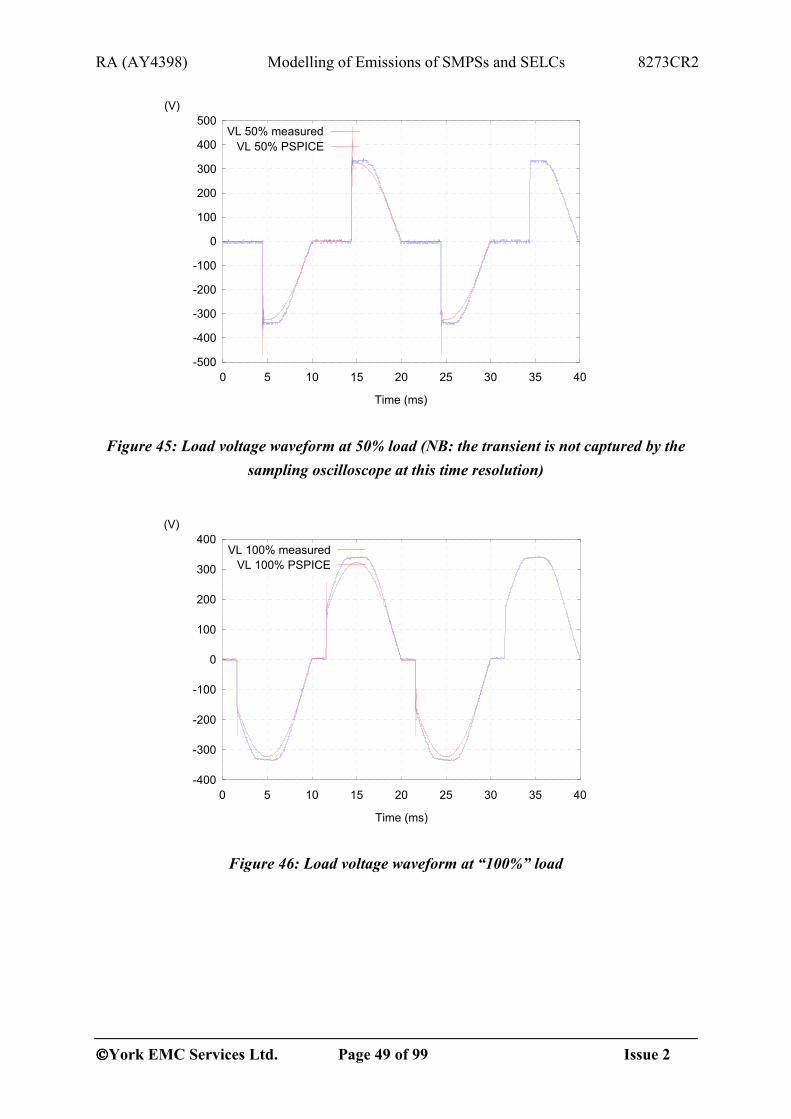
5.2.7 Predicted and measured results
5.2.7.1 Operating waveforms Measurement of the operating waveforms was achieved by powering the unit though a mains isolation transformer allowing various parts of the circuit to be grounded during measurement. It can be seen in the measured waveforms that the sinusoidal waveforms have

RA (AY4398) Modelling of Emissions of SMPSs and SELCs 8273CR2
York EMC Services Ltd. Page 48 of 99 Issue 2
a flattened top – this is probably due to the isolating transformer core approaching saturation. The leakage inductance of the transformer may also affect the measured waveforms and will certainly present different supply impedance at high frequencies to the LISN used for measurement. The capacitance of the X10 and X100 oscilloscope probes used may also affect the measured waveforms.
A sampling oscilloscope was used to record the time-domain circuit waveforms – however the number of samples available was not high enough to record a whole cycle of the waveform simultaneously with detail of the switching transients. The switching angle was measured from the sampled waveforms and used with the component measurements to construct a suitable PSPICE model.
Figure 44: Measuring the dimmer operating waveforms (isolating transformer not shown)
RA (AY4398) Modelling of Emissions of SMPSs and SELCs 8273CR2
York EMC Services Ltd. Page 49 of 99 Issue 2
-500
-400
-300
-200
-100
0
100
200
300
400
500
0 5 10 15 20 25 30 35 40
(V)
Time (ms)
VL 50% measuredVL 50% PSPICE
Figure 45: Load voltage waveform at 50% load (NB: the transient is not captured by the sampling oscilloscope at this time resolution)
-400
-300
-200
-100
0
100
200
300
400
0 5 10 15 20 25 30 35 40
(V)
Time (ms)
VL 100% measuredVL 100% PSPICE
Figure 46: Load voltage waveform at “100%” load

RA (AY4398) Modelling of Emissions of SMPSs and SELCs 8273CR2
York EMC Services Ltd. Page 50 of 99 Issue 2
-500
-450
-400
-350
-300
-250
-200
-150
-100
-50
0
50
0 50 100 150 200
(V)
Time (us)
MeasuredPSPICE
Figure 47: Load voltage waveform at 50% load showing negative switching transient
Figure 47 shows the transient switching behaviour of the initial PSPICE model. The magnitude of the transient depends upon the switching speed of the triac and the inductance of the series choke. The frequency of oscillation depends on the inductance of the choke and any parasitic capacitances. By reducing the choke inductance and increasing the triac switching time, the measured waveform could be reproduced more accurately as shown in Figure 48. However, as can be seen below – the initial model gives conducted emissions results which are closer to the measured values than the model of Figure 48. This may be due to the fact that the switching speed and transient behaviour depends mostly on the inductor and it’s stray capacitance. With additional capacitance due to the scope probe and possibly additional inductance due to the isolation transformer – the measured switching transient may be different from that which occurs without the isolation transformer and oscilloscope probe.

RA (AY4398) Modelling of Emissions of SMPSs and SELCs 8273CR2
York EMC Services Ltd. Page 51 of 99 Issue 2
-400
-350
-300
-250
-200
-150
-100
-50
0
50
0 50 100 150 200
(V)
Time (us)
MeasuredPSPICE
Figure 48: Load voltage waveform at 50% load showing negative switching transient when the choke is reduced to 300µµµµH and the switching time is increased to 30µµµµs
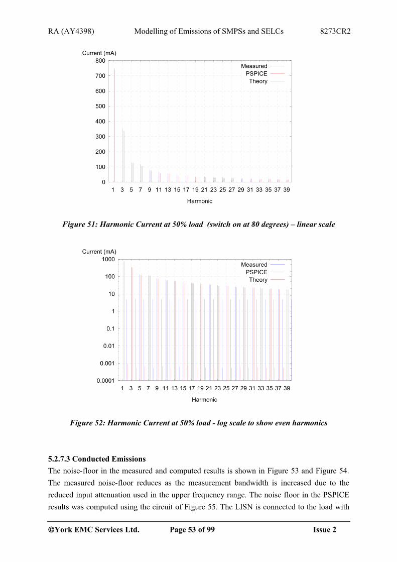
5.2.7.2 Harmonic Current The conducted emissions were computed using a simulation of 30ms duration (one and a half mains cycles). The first 10ms was disregarded as it contains voltage transients due to the LISN network. The last 20ms was used with a print time step of 15ns, which gives sufficient detail to allow a spectrum up to 33.33MHz to be computed. A matlab/octave script was used to process the PSPICE time-domain data (Appendix 1 – Computation of Conducted Emissions). Since a FFT of 20ms of data produces data points at 50Hz these can be used directly for the harmonic data.
Since harmonic current measurements require relatively low frequency harmonics (up to 2kHz) modelling sufficient detail in the waveforms is simple compared with the conducted interference case. The Harmonic currents measured, from the PSPICE model, and from the analytical solution presented previously are shown below. In general the accuracy is very good. The main difference between the measured and other results is the presence of even harmonics in the measured data. The analytic and PSPICE models assume perfect symmetry in the switching device – thus even harmonics are not possible. In the real device some asymmetry will usually exist in the triac or diac so a small amount of even harmonics is present – this is at least an order of magnitude less than the odd-harmonics so this error is unlikely to be of great importance in most situations.

RA (AY4398) Modelling of Emissions of SMPSs and SELCs 8273CR2
York EMC Services Ltd. Page 52 of 99 Issue 2
0
200
400
600
800
1000
1200
1 3 5 7 9 11 13 15 17 19 21 23 25 27 29 31 33 35 37 39
Current (mA)
Harmonic
MeasuredPSPICE
Theory
Figure 49: Harmonic Current at 100% load (switch on at 29 degrees) – linear scale
0.0001
0.001
0.01
0.1
1
10
100
1000
10000
1 3 5 7 9 11 13 15 17 19 21 23 25 27 29 31 33 35 37 39
Current (mA)
Harmonic
MeasuredPSPICE
Theory
Figure 50: Harmonic Current at 100% load - log scale to show even harmonics
RA (AY4398) Modelling of Emissions of SMPSs and SELCs 8273CR2
York EMC Services Ltd. Page 53 of 99 Issue 2
0
100
200
300
400
500
600
700
800
1 3 5 7 9 11 13 15 17 19 21 23 25 27 29 31 33 35 37 39
Current (mA)
Harmonic
MeasuredPSPICE
Theory
Figure 51: Harmonic Current at 50% load (switch on at 80 degrees) – linear scale
0.0001
0.001
0.01
0.1
1
10
100
1000
1 3 5 7 9 11 13 15 17 19 21 23 25 27 29 31 33 35 37 39
Current (mA)
Harmonic
MeasuredPSPICE
Theory
Figure 52: Harmonic Current at 50% load - log scale to show even harmonics
5.2.7.3 Conducted Emissions The noise-floor in the measured and computed results is shown in Figure 53 and Figure 54. The measured noise-floor reduces as the measurement bandwidth is increased due to the reduced input attenuation used in the upper frequency range. The noise floor in the PSPICE results was computed using the circuit of Figure 55. The LISN is connected to the load with

RA (AY4398) Modelling of Emissions of SMPSs and SELCs 8273CR2
York EMC Services Ltd. Page 54 of 99 Issue 2
the dimmer circuit entirely removed. The noise in PSPICE is due to the finite precision of the time-domain data exported from the simulation, numerical errors in the PSICE computation, and the effect of the strong 50Hz component in the LISN live line output. The number of digits (the default is 4) in the output file was varied to determine the effect on the noise floor. Although the relative tolerance parameter, which determines the point at which the iterative solution is said to have converged, was left at its default value of 10-3, the use of six or eight digits of precision in the output file improved the noise floor considerably.
-100
-80
-60
-40
-20
0
20
40
60
80
0.01 0.1 1 10 100
(dBuV)
Frequency (MHz)
Measurement noise floorPSPICE L Noise - 4 digitsPSPICE L Noise - 6 digitsPSPICE L Noise - 8 digits
Figure 53: PSPICE and measurement noise floor – peak measurement
-100
-80
-60
-40
-20
0
20
40
60
80
0.01 0.1 1 10 100
(dBuV)
Frequency (MHz)
Measurement noise floorPSPICE L Noise - 4 digitsPSPICE L Noise - 6 digitsPSPICE L Noise - 8 digits
Figure 54: PSPICE and measurement noise floor – average measurement

RA (AY4398) Modelling of Emissions of SMPSs and SELCs 8273CR2
York EMC Services Ltd. Page 55 of 99 Issue 2
The PSPICE Neutral line has less noise than the Live in all cases. This is due to the fact that the Live Line has a 50Hz component which is much larger than any of the conducted interference components. The results below use 6 digits of output precision to ensure that the PSPICE noise floor is below that of the measurement system.
Figure 55: Circuit used for PSPICE noise floor computation.
In a circuit such as this where no earth conductors are used, the live and neutral line conducted interference should be virtually identical – this was indeed the case (Figure 56 and Figure 57). Any small differences are due to parasitic capacitances to ground, which are not modelled, mismatch between the LISN channels, and the effect of the 50Hz component in the LISN line output which may affect the FFT accuracy in the model.

RA (AY4398) Modelling of Emissions of SMPSs and SELCs 8273CR2
York EMC Services Ltd. Page 56 of 99 Issue 2
10
20
30
40
50
60
70
80
90
100
0.01 0.1 1 10 100
(dBuV)
Frequency (MHz)
Measured L averageMeasured L peak
Measured N averageMeasured N peak
Figure 56: Measured Conducted Interference on the Live and Neutral terminals at 50% load
-60
-40
-20
0
20
40
60
80
100
0.01 0.1 1 10 100
(dBuV)
Frequency (MHz)
PSPICE L averagePSPICE L peak
PSPICE N averagePSPICE N peak
Figure 57: Computed (PSPICE) Conducted Interference on the Live and Neutral terminals at 50% load (model with original measured parameters)
The measured results are compared with the PSPICE model, constructed using the measured component values and measures switching phase, in Figure 58 (average) and Figure 59 (peak). It can be seen that the measured value reached the noise floor at about 1MHz in the case of the average data. The measurement appears to remain above the noise floor in the case of the peak values. The PSPICE results are similar but differences of up to 10dB from

RA (AY4398) Modelling of Emissions of SMPSs and SELCs 8273CR2
York EMC Services Ltd. Page 57 of 99 Issue 2
the measured results occur in the average case becoming larger in the peak case. The PSPICE results appear to be above the (PSPICE) noise floor over the entire frequency range – however the structure in these results between 2 and 30MHz appears to be due to numerical noise rather than any aspect of the circuit.
-60
-40
-20
0
20
40
60
80
100
0.01 0.1 1 10 100
(dBuV)
Frequency (MHz)
Measured L AvePSPICE L AveAverage Limit
Measurement noise floorPSPICE L Noise floor
Figure 58: Average Conducted Interference on the Live terminal at 50% load
-40
-20
0
20
40
60
80
100
0.01 0.1 1 10 100
(dBuV)
Frequency (MHz)
Measured L PeakPSPICE L Peak
Quasi-peak LimitMeasurement noise floor
PSPICE L Noise floor
Figure 59: Peak Conducted Interference on the Live terminal at 50% load

RA (AY4398) Modelling of Emissions of SMPSs and SELCs 8273CR2
York EMC Services Ltd. Page 58 of 99 Issue 2
-40
-20
0
20
40
60
80
100
0.01 0.1 1 10 100
(dBuV)
Frequency (MHz)
Measured L (YES)PSPICE L - 1us
PSPICE L - 0.5usPSPICE L - 8us
Measurement noise floor
Figure 60: Effect of “thyristor” switching speed on Average Conducted Interference at 50% load
In order to determine the dominant factor in determining the conducted interference spectrum, the effect of switching time and the filter components were examined. It can be seen, in Figure 60, that for switching time constants of 1µs and 0.5µs the spectra remains practically identical up to 2 MHz, whilst the 8µs switching time constant shows a faster roll-off. For the 1µs and 0.5µs switching time constants the inductor/capacitor filter dominates the behaviour, whereas for the 8µs switching time constant, the roll-off of the pulse spectrum due to the slower switching becomes apparent.
Figure 61 shows the predicted peak conducted interference spectrum for the controller model with reduced inductance and increased switching time. These changes were made to produce a load voltage waveform more nearly matching the measured value (Figure 48). It can be seen that the slow rise time dominates the spectrum and gives a poor result compared with the original model (Figure 59).

RA (AY4398) Modelling of Emissions of SMPSs and SELCs 8273CR2
York EMC Services Ltd. Page 59 of 99 Issue 2
-60
-40
-20
0
20
40
60
80
100
0.01 0.1 1 10 100
(dBuV)
Frequency (MHz)
Measured L PeakPSPICE L - Reduced L 30us
Measurement noise floorPSPICE L Noise floor
Figure 61: Peak Conducted Interference on the Live terminal at 50% load when the choke is reduced to 300µµµµH and the switching time is increased to 30µµµµs
Figure 62 shows the effect of removing the LC filter. It can be seen that, for fast switching case (0.5µs time constant) the level of conducted interference is greatly increased and is now above the allowed limit. In the case of a slow switching speed (30µs time constant), the spectrum falls well below the measured level and limit line. In practice, the SCR switching time is unknown and variable, but likely to be of the order of 1µs, so that the filter is necessary to control the interference spectrum.

RA (AY4398) Modelling of Emissions of SMPSs and SELCs 8273CR2
York EMC Services Ltd. Page 60 of 99 Issue 2
-40
-20
0
20
40
60
80
100
120
140
0.01 0.1 1 10 100
(dBuV)
Frequency (MHz)
Measured L PeakPSPICE L - No LC 30us
PSPICE L - No LC L 0.5usQuasi-peak Limit
Measurement noise floorPSPICE L Noise floor
Figure 62: Peak Conducted Interference on the Live terminal at 50% load when the L C filter is removed with the switching time constant equal to 0.5µµµµs and 30µµµµs
Figure 63 compares the simple analytic result determined by the product of the zero rise time spectrum multiplied by the filter and LISN transfer functions (Matlab zero rise including filter and LISN). This follows closely the PSPICE prediction up to 2MHz. Above 2MHz the simple analytic approximation of the conducted interference begins to rise, due to the imperfections in the filter – this is not visible in the measured result, due to the noise floor. It is also not visible in the PSPICE results. Also shown is a simple analytic result with a 3µs rise-time trapezoidal modulating pulse, which has a similar structure to the measured spectrum, but even when multiplied by the Filter/LISN transfer function does not produce levels similar to those measured.

RA (AY4398) Modelling of Emissions of SMPSs and SELCs 8273CR2
York EMC Services Ltd. Page 61 of 99 Issue 2
-60
-40
-20
0
20
40
60
80
100
0.01 0.1 1 10 100
(dBuV)
Frequency (MHz)
Measured L AvePSPICE L Ave
Matlab zero rise timeMatlab 3.0us rise time
Matlab zero rise inc. Filter & LISNMeasurement noise floor
Figure 63: Average Conducted Interference on the Live terminal at 50% load Approximate prediction v measured and PSPICE simulation
Figure 64 shows the measured and predicted peak conducted emissions at 100% load. With the dimmer used there is still a 29degree switching delay when the control is set to full power, so significant interference is still generated. Whilst the original PSPICE model produces a reasonable approximation to the measured result, it is apparent that the roll-off in the measured spectrum at 0.02MHz is more rapid than in the 50% load case. This implies that the rise time of the switching waveform has increased and is beginning to dominate the spectrum.

RA (AY4398) Modelling of Emissions of SMPSs and SELCs 8273CR2
York EMC Services Ltd. Page 62 of 99 Issue 2
-40
-20
0
20
40
60
80
100
0.01 0.1 1 10 100
(dBuV)
Frequency (MHz)
Measured L PeakPSPICE L Peak
Quasi-peak LimitMeasurement noise floor
PSPICE L Noise floor
Figure 64: Peak Conducted Interference on the Live terminal at 100% load – original circuit with 1µµµµs switching time-constant
In Figure 65 the switching time-constant has been increased to 60µs. It can be seen that the initial roll-off of the PSPICE model now matches that of the measured spectrum. However the measured spectrum then levels out, whilst the PSPICE spectrum does not.
Two possible reasons for the change in the spectrum roll-off at 100% load are:
1. the triac switches more slowly due to the lower switching voltage and current but there is some other feature generating noise at higher frequencies;
2. the filter choke exhibits a larger inductance at lower current (further from saturation) giving a lower roll-off frequency.

RA (AY4398) Modelling of Emissions of SMPSs and SELCs 8273CR2
York EMC Services Ltd. Page 63 of 99 Issue 2
-40
-20
0
20
40
60
80
100
0.01 0.1 1 10 100
(dBuV)
Frequency (MHz)
Measured L PeakPSPICE L Peak
Quasi-peak LimitMeasurement noise floor
PSPICE L Noise floor
Figure 65: Peak Conducted Interference on the Live terminal at 100% load when the switching time-constant is increased to 60µµµµs
5.3 Item 5: Printer power supply
2332/sch/10 d
Printer PSU
A3
1 1Tuesday, March 04, 2003
Title
Size Document Number Rev
Date: Sheet of
NOTE:- Transformer windings shown are approximate and relateto a conductivity test only. Position of taps relativeto each other has not been tested, and may differ tothat shown.- Component values or identifiers marked "?" are unknown
?AF1
1 2
CX10.1uF
12
FL1Choke
15
48
D8
1N4007
1 2
D41N4007
1 2
D31N4007
1 2
D21N4007
12
D11N4007
12
C11102(1nF)
12
L
1
N
1
C82.2nF
12
C11?
12
Q1HNC60F
1
23
R2A51k
21
R5A100k
21
R4A12k
21
J1Link
C52220uF
12
D51N4007
12
R5B15k4
21
R116k2
21
R2B51k
21
L?Bead1 2
D13
?
1 2
TR12N4401
1
2
3
L?Bead1 2
R4B12k
21
R52A1k
21
L?Bead
12
C51?
1 2
R151R
21
ZD1
?
12
R91k
21
R51150R
21U?
DAP07
11
22
33
44
556 67 788
ZD51?
12
R10R51
21
C12?
1 2
R1351R
21
C4?
12
C9?
12
R6887R
21
C21nF
12
R52B1k
21
D61N4007
12
R82k7
21
C5?
12
FL51Choke
15
48 Vo
1
Gnd1
C110uF
12
Figure 66: SMPS circuit diagram of Item 5

RA (AY4398) Modelling of Emissions of SMPSs and SELCs 8273CR2
York EMC Services Ltd. Page 64 of 99 Issue 2
5.3.1 Common mode choke
The common-mode choke model of Figure 13 was implemented as a library element for use with this and other models.
5.3.2 Capacitor models
The capacitor model of Figure 1 was implemented as a library element and used to represent the majority of capacitors in the circuits (additional parasitic elements using the ideal capacitor model being the only exception). As described in Section 4, two capacitors were needed in some cases to adequately represent the behaviour of some circuit capacitors.
5.3.3 Switch transistor and drive circuit model
An ideal switch model with a parasitic capacitance (CSW) and series resistance (RS) driven by a pulsed trapezoidal voltage source was used to represent the switching transistor and its drive circuit. No attempt was made to simulate the PWM and feedback circuits within the power supply. The circuit developed allows the switching frequency and duty cycle to be accurately set.
5.3.4 Transformer model
A simple, linear, coupled inductor (library) model was used to represent the transformer. Only the primary and a single low-voltage secondary were modelled. The following parasitic elements were added:
• Shunt (parallel) capacitance: CTP is connected across the primary winding;
• Shunt resistance: RTP connected across the primary winding;
• Mutual coupling capacitance: between the primary and secondary windings (CTCa and CTCb);
• Series resistance of the primary winding (RS);
• An additional capacitance to VSS (CDG) to represent the capacitance between the primary and HV secondary windings.
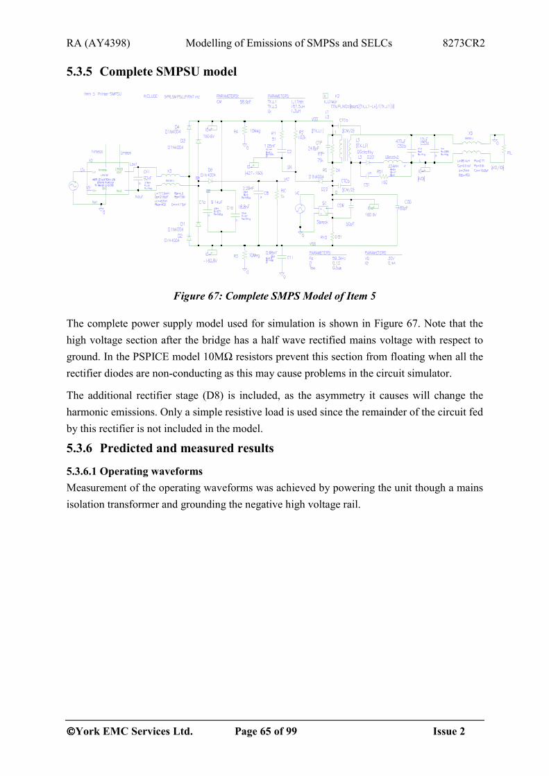
RA (AY4398) Modelling of Emissions of SMPSs and SELCs 8273CR2
York EMC Services Ltd. Page 65 of 99 Issue 2
5.3.5 Complete SMPSU model
Figure 67: Complete SMPS Model of Item 5
The complete power supply model used for simulation is shown in Figure 67. Note that the high voltage section after the bridge has a half wave rectified mains voltage with respect to ground. In the PSPICE model 10MΩ resistors prevent this section from floating when all the rectifier diodes are non-conducting as this may cause problems in the circuit simulator.
The additional rectifier stage (D8) is included, as the asymmetry it causes will change the harmonic emissions. Only a simple resistive load is used since the remainder of the circuit fed by this rectifier is not included in the model.
5.3.6 Predicted and measured results
5.3.6.1 Operating waveforms Measurement of the operating waveforms was achieved by powering the unit though a mains isolation transformer and grounding the negative high voltage rail.

RA (AY4398) Modelling of Emissions of SMPSs and SELCs 8273CR2
York EMC Services Ltd. Page 66 of 99 Issue 2
0
50
100
150
200
250
300
350
400
450
500
-10 -5 0 5 10 15 20
(V)
Time (us)
MeasuredPSPICE
Figure 68: FET (switch) drain voltage waveform at 50% load fs=59.3kHz D=0.095 (D is the duty cycle, i.e. the proportion of the cycle for which the switch is on)
Figure 68 shows the FET (switch) drain voltage waveform at 50% load. The simulation model was set to the measured switching frequency and duty cycle. The switching time and parasitic elements on the switch were adjusted to obtain an approximate fit to the observed waveform.

RA (AY4398) Modelling of Emissions of SMPSs and SELCs 8273CR2
York EMC Services Ltd. Page 67 of 99 Issue 2
-0.1
0
0.1
0.2
0.3
0.4
0.5
0.6
0.7
0.8
-10 -5 0 5 10 15 20
(A)
Time (us)
MeasuredPSPICE
Figure 69: Transformer primary current waveform at 50% load PSPICE: fs=59.3kHz D=0.095
Figure 69 shows the primary current waveform at 50% load. The switch parasitic capacitance in the model was adjusted to achieve correspondence in the initial current transient. The inductance of the primary was adjusted to achieve a value close to the measured peak primary (top of triangle) current.
Figure 70 shows the FET drain voltage waveform for 100% load and Figure 71 shows the corresponding primary current waveform.
It can be seen that there is a good correspondence in the features seen in the model and measured waveforms. However, it was not possible to exactly replicate the transient features. Also, it should be noted that in the model the waveform was fixed throughout the mains cycle whereas the internal feedback in the real power supply adjusted the switching waveform to counter the mains ripple on the rectified mains supply to maintain a constant output.

RA (AY4398) Modelling of Emissions of SMPSs and SELCs 8273CR2
York EMC Services Ltd. Page 68 of 99 Issue 2
0
50
100
150
200
250
300
350
400
450
500
-10 -5 0 5 10 15 20
(V)
Time (us)
MeasuredPSPICE
Figure 70: FET (switch) drain voltage waveform at 100% load fs=59.3kHz D=0.122
-0.1
0
0.1
0.2
0.3
0.4
0.5
0.6
0.7
0.8
-10 -5 0 5 10 15 20
(A)
Time (us)
MeasuredPSPICE
Figure 71: Transformer primary current waveform at 100% load fs=59.3kHz D=0.122
5.3.6.2 Harmonic Current The conducted emissions were computed using a simulation of 30ms duration (one and a half mains cycles). The first 10ms was disregarded as it contains voltage transients due to the LISN network. The last 20ms was used with a print time step of 15ns which gives sufficient detail to allow a spectrum up to 33.33MHz to be computed. A matlab/octave script was used to process the PSPICE time-domain data (Appendix1 – Computation of Conducted

RA (AY4398) Modelling of Emissions of SMPSs and SELCs 8273CR2
York EMC Services Ltd. Page 69 of 99 Issue 2
Emissions). Since a FFT of 20ms of data produces data points at 50Hz these can be used directly for the harmonic data.
The harmonic currents in a circuit with a rectifier depend mainly upon the stray inductance and resistance in the rectifier circuit, also the diode and capacitor characteristics. Whilst the capacitor characteristics were measured, the exact diode type and characteristics were unknown - a 1N4004 model was used. No attempt was made to consider the effect of stray inductance and resistance of the rectifier circuit. The LISN and mains impedance models used determine the supply impedance. Given these limitations the PSPICE predictions are surprisingly close to the measured results.
The asymmetry introduced by the additional half-wave rectifier does not produce significant even harmonic content in the model when seen on a linear scale.
0
10
20
30
40
50
60
70
80
1 3 5 7 9 11 13 15 17 19 21 23 25 27 29 31 33 35 37 39
Current (mA)
Harmonic
MeasuredPSPICE
Figure 72: Harmonic Current at 100% load
When seen on a logarithmic scale, it can be seen that even harmonic components are present in both measured and predicted results. The measured levels are an order of magnitude higher than in the simulation however as the running load on the additional rectifier stage (the probable cause of asymmetry) was estimated with poor accuracy this is not unexpected.
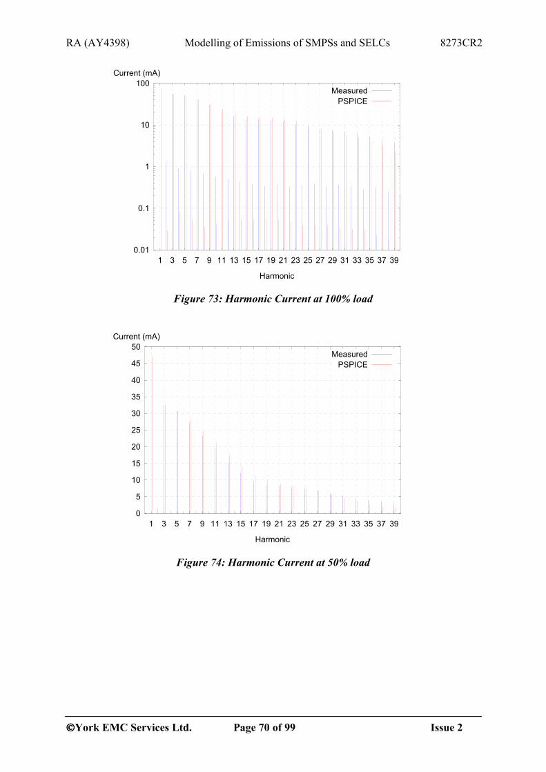
RA (AY4398) Modelling of Emissions of SMPSs and SELCs 8273CR2
York EMC Services Ltd. Page 70 of 99 Issue 2
0.01
0.1
1
10
100
1 3 5 7 9 11 13 15 17 19 21 23 25 27 29 31 33 35 37 39
Current (mA)
Harmonic
MeasuredPSPICE
Figure 73: Harmonic Current at 100% load
0
5
10
15
20
25
30
35
40
45
50
1 3 5 7 9 11 13 15 17 19 21 23 25 27 29 31 33 35 37 39
Current (mA)
Harmonic
MeasuredPSPICE
Figure 74: Harmonic Current at 50% load

RA (AY4398) Modelling of Emissions of SMPSs and SELCs 8273CR2
York EMC Services Ltd. Page 71 of 99 Issue 2
0.01
0.1
1
10
100
1 3 5 7 9 11 13 15 17 19 21 23 25 27 29 31 33 35 37 39
Current (mA)
Harmonic
MeasuredPSPICE
Figure 75: Harmonic Current at 50% load
5.3.6.3 Conducted Emissions The conducted emissions were computed using a simulation of 30ms duration (one and a half mains cycles). The first 10ms was disregarded as it contains voltage transients due to the LISN network. The last 20ms was used with a print time step of 15ns which gives sufficient detail to allow a spectrum up to 33.33MHz to be computed. An octave/matlab script was used to process the PSPICE time-domain data (Appendix1 – Computation of Conducted Emissions). For the conducted data the power spectrum was averaged over the appropriate bandwidth to obtain the conducted emissions data.
Figure 76 shows the measured and simulated peak conducted interference at 100% load. The general shapes of the curves are similar but the levels differ considerably, particularly above 150kHz where the step in measurement data (≈9dB) is rather smaller than the step in simulated data (≈33dB). The measurement bandwidth increases from 200Hz to 9kHz at 150kHz and this implies an increase in energy in the detector of between 9000/200 or 16.5dB for uncorellated harmonics (noise like signal) and (9000/200)2 or 33dB for coherent harmonics (e.g. see Figure 59 for the dimmer). The 11dB fall in the noise floor could account for this if the signal was below the noise floor by about 22dB before 150kHz, it would appear about 11 dB above the noise floor after 150kHz. The peak data is also likely to be more sensitive to the phase relationship between harmonics than the average data.

RA (AY4398) Modelling of Emissions of SMPSs and SELCs 8273CR2
York EMC Services Ltd. Page 72 of 99 Issue 2
0
20
40
60
80
0.01 0.1 1 10 100
(dBuV)
Frequency (MHz)
Measured L PeakPSPICE L Peak
Quasi-peak LimitMeasurement noise floor
Figure 76: Peak Conducted Interference on the Live terminal at 100% load
Figure 77 shows the measured and simulated average conducted interference at 100% load. Again, the features are similar but a significant discrepancy in the levels occurs. The measurement data experiences a fall of ≈8 dB as the measurement bandwidth increases, whilst the simulation shows a rise of ≈8 dB. Again, this appears to be due to the fall in measurement noise floor as the measurement bandwidth rises (due to reduction in attenuator setting).
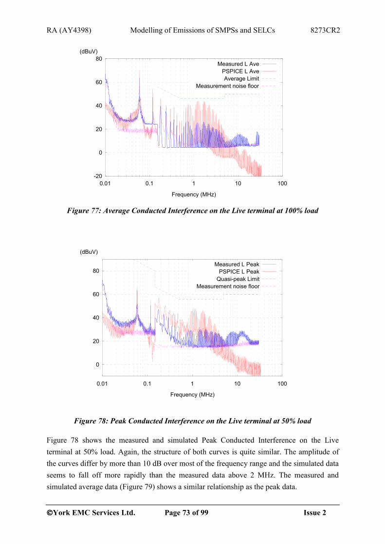
RA (AY4398) Modelling of Emissions of SMPSs and SELCs 8273CR2
York EMC Services Ltd. Page 73 of 99 Issue 2
-20
0
20
40
60
80
0.01 0.1 1 10 100
(dBuV)
Frequency (MHz)
Measured L AvePSPICE L AveAverage Limit
Measurement noise floor
Figure 77: Average Conducted Interference on the Live terminal at 100% load
0
20
40
60
80
0.01 0.1 1 10 100
(dBuV)
Frequency (MHz)
Measured L PeakPSPICE L Peak
Quasi-peak LimitMeasurement noise floor
Figure 78: Peak Conducted Interference on the Live terminal at 50% load
Figure 78 shows the measured and simulated Peak Conducted Interference on the Live terminal at 50% load. Again, the structure of both curves is quite similar. The amplitude of the curves differ by more than 10 dB over most of the frequency range and the simulated data seems to fall off more rapidly than the measured data above 2 MHz. The measured and simulated average data (Figure 79) shows a similar relationship as the peak data.

RA (AY4398) Modelling of Emissions of SMPSs and SELCs 8273CR2
York EMC Services Ltd. Page 74 of 99 Issue 2
-20
0
20
40
60
80
0.01 0.1 1 10 100
(dBuV)
Frequency (MHz)
Measured L AvePSPICE L AveAverage Limit
Measurement noise floor
Figure 79: Average Conducted Interference on the Live terminal at 50% load
-20
0
20
40
60
80
0.01 0.1 1 10 100
(dBuV)
Frequency (MHz)
Measured L AvePSPICE L Ave 0.03us rise
PSPICE L Ave 0.3us risePSPICE L Ave 3us rise
Measurement noise floor
Figure 80: Average Conducted Interference on the Live terminal at 100% load –effect of switch time-constant
In order to investigate the effect of switching time on the high frequency spectrum the 100% load simulation was re-run with the switching time constant set to 0.03µs and 3µs, an order of magnitude faster and slower than the 0.3µs used in the main set of simulations. Figure 80 shows the effect of the switch time-constant on the spectrum: The faster (0.03µs) switching time constant produces a spectrum which falls off slowly with increasing frequency – closer to the measured spectrum than the original (0.3µs time constant). Increasing the switching

RA (AY4398) Modelling of Emissions of SMPSs and SELCs 8273CR2
York EMC Services Ltd. Page 75 of 99 Issue 2
time (3µs time constant) produces a spectrum, which falls off earlier. The overall level of the interference spectrum prior to the high frequency roll-off due to the switching time, remains largely the same regardless of switching time. Figure 81 shows the effect of switch rise-time on the current waveform in R10.
-0.5
0
0.5
1
1.5
2
-2 -1 0 1 2
(A)
Time (us)
MeasuredPSPICE 0.3us
PSPICE 0.03usPSPICE 3us
Figure 81: Effect of rise-time on transformer R10 current waveform
10
20
30
40
50
60
70
80
0.01 0.1 1 10 100
(dBuV)
Frequency (MHz)
Measured L 100% PeakMeasured L 50% Peak
Quasi-peak LimitMeasurement noise floor
Figure 82: Measured Peak Conducted Interference on the Live terminal

RA (AY4398) Modelling of Emissions of SMPSs and SELCs 8273CR2
York EMC Services Ltd. Page 76 of 99 Issue 2
Figure 82 shows the relationship between the measured peak interference at 100% and 50% load and Figure 83 shows the same curves for simulated data. The relative levels of interference in the simulated data agree with the measured data.
-10
0
10
20
30
40
50
60
70
80
0.01 0.1 1 10 100
(dBuV)
Frequency (MHz)
PSPICE L 100% PeakPSPICE L 50% Peak
Quasi-peak Limit
Figure 83: PSPICE Peak Conducted Interference on the Live terminal
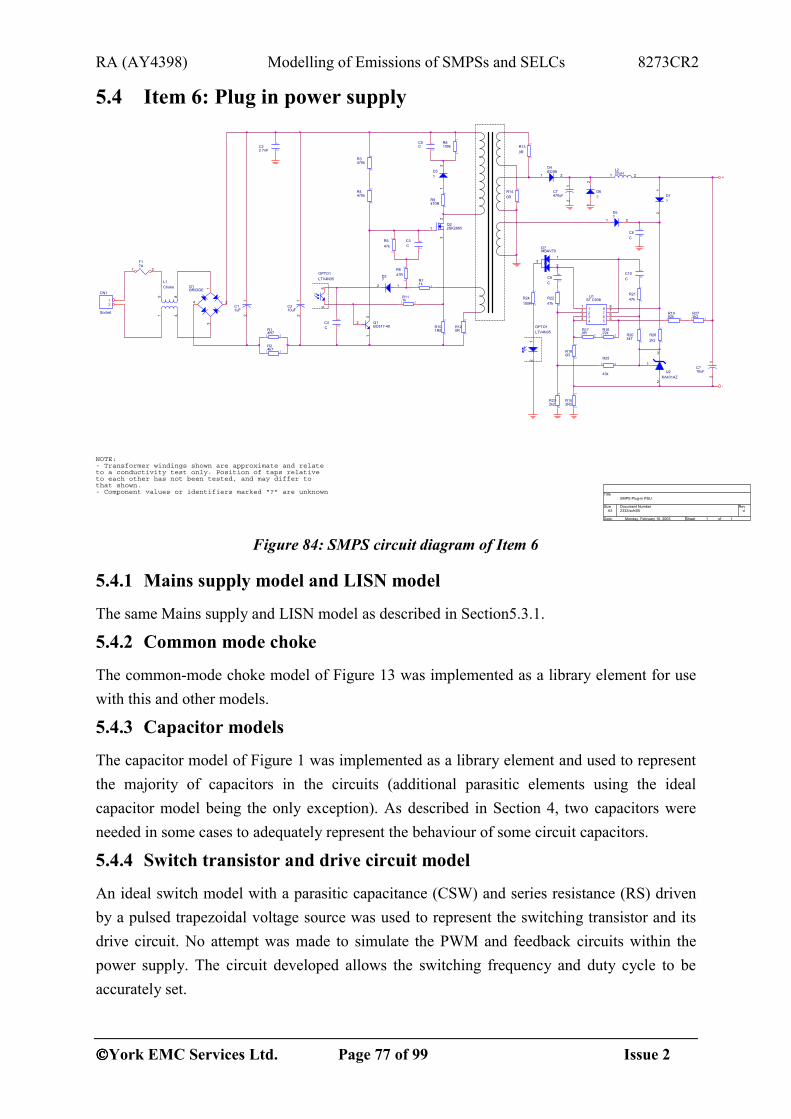
RA (AY4398) Modelling of Emissions of SMPSs and SELCs 8273CR2
York EMC Services Ltd. Page 77 of 99 Issue 2
5.4 Item 6: Plug in power supply
2332/sch/05 d
SMPS Plug-in PSU
A3
1 1Monday, February 10, 2003
Title
Size Document Number Rev
Date: Sheet of
+
-
NOTE:- Transformer windings shown are approximate and relateto a conductivity test only. Position of taps relativeto each other has not been tested, and may differ tothat shown.- Component values or identifiers marked "?" are unknown
CN1
Socket
12
?AF1
1 2
L1Choke
15
48
C11uF
12
C3C
12
C210uF
12
R111k
21
C5C
12
D2?
12
L222uH1 2
D5?
1 2
C8C
12
R3470k
21
R4470k
21
Q1BC817-40
1
2
3
R71k
21
R647R
21
R8100k
21
C22.7nF
12
R262k2 2
1
R24100R 2
1
R130R
21
R272k2
21
D6?
12
R204k7 2
1
D7?
12
C7470uF
12
C?10uF
12
C10C
12
R2147k 2
1
R180R 2
1
R232k2 2
1
R170R
21
R1622k
21
OPTO1LTV4N35
12
R1982k
21
R152R2 2
1
D1BRIDGE
- +
1
2
3
4
R14R7
21
R24k7
21
R547k
21
C4C
12
OPTO1LTV4N35
54
R101R5 2
1
R120R 2
1
D3?
12
R9470R 2
1
Q22SK28651
23
U1ST C938
11
22
33
44 5 56 6778 8
D?MBAV70
13
2
C9C
12
R2247k 2
1
D4EC9B
1 2
R25
43k
21
U2KA431AZ
3
1
2
R140R
21
Figure 84: SMPS circuit diagram of Item 6
5.4.1 Mains supply model and LISN model
The same Mains supply and LISN model as described in Section5.3.1.
5.4.2 Common mode choke
The common-mode choke model of Figure 13 was implemented as a library element for use with this and other models.
5.4.3 Capacitor models
The capacitor model of Figure 1 was implemented as a library element and used to represent the majority of capacitors in the circuits (additional parasitic elements using the ideal capacitor model being the only exception). As described in Section 4, two capacitors were needed in some cases to adequately represent the behaviour of some circuit capacitors.
5.4.4 Switch transistor and drive circuit model
An ideal switch model with a parasitic capacitance (CSW) and series resistance (RS) driven by a pulsed trapezoidal voltage source was used to represent the switching transistor and its drive circuit. No attempt was made to simulate the PWM and feedback circuits within the power supply. The circuit developed allows the switching frequency and duty cycle to be accurately set.

RA (AY4398) Modelling of Emissions of SMPSs and SELCs 8273CR2
York EMC Services Ltd. Page 78 of 99 Issue 2
5.4.5 Transformer model
A simple, linear, coupled inductor (library) model was used to represent the transformer. Only the primary and a single low-voltage secondary were modelled. The following parasitic elements were added:
Shunt (parallel) capacitance: CTP is connected across the primary winding;
Shunt resistance: RTP connected across the primary winding;
Mutual coupling capacitance: between the primary and secondary windings (CTCa and CTCb).
5.4.6 Complete SMPS model
Figure 85: Complete SMPS Model of Item 6
The complete power supply model used for simulation is shown in Figure 85. Note that the high voltage section after the bridge has a half wave rectified mains voltage with respect to ground. In the PSPICE model 10 MΩ resistors prevent this section from floating when all the rectifier diodes are non-conducting as this may cause problems in the circuit simulator.
5.4.7 Predicted and measured results
5.4.7.1 Operating waveforms Measurement of the operating waveforms was achieved by powering the unit though a mains isolation transformer and grounding the negative high voltage rail.
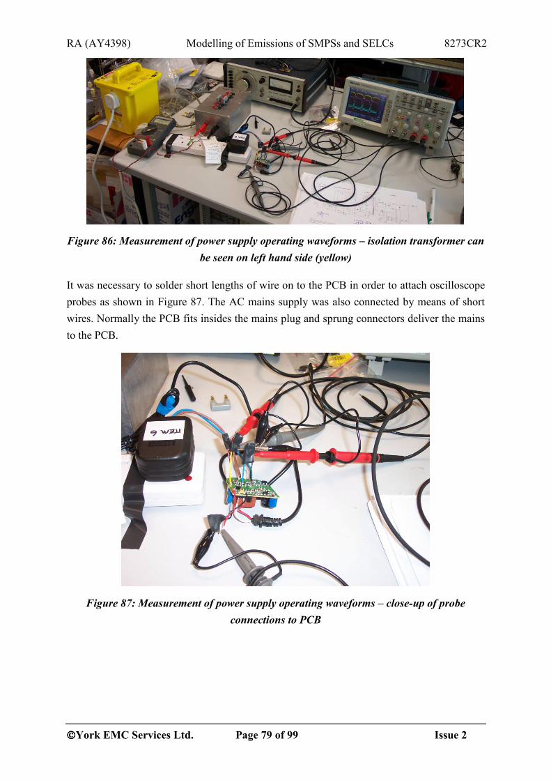
RA (AY4398) Modelling of Emissions of SMPSs and SELCs 8273CR2
York EMC Services Ltd. Page 79 of 99 Issue 2
Figure 86: Measurement of power supply operating waveforms – isolation transformer can be seen on left hand side (yellow)
It was necessary to solder short lengths of wire on to the PCB in order to attach oscilloscope probes as shown in Figure 87. The AC mains supply was also connected by means of short wires. Normally the PCB fits insides the mains plug and sprung connectors deliver the mains to the PCB.
Figure 87: Measurement of power supply operating waveforms – close-up of probe connections to PCB

RA (AY4398) Modelling of Emissions of SMPSs and SELCs 8273CR2
York EMC Services Ltd. Page 80 of 99 Issue 2
0
50
100
150
200
250
300
350
400
450
500
-15 -10 -5 0 5 10 15
FET Drain (V)
Time (us)
MeasuredPSPICE
Figure 88: FET (switch) drain voltage waveform at 50% load fs=131.7kHz D=0.145
Figure 88 shows the FET (switch) drain voltage waveform at 50% load. The simulation model was set to the measured switching frequency and duty cycle. The switching time and parasitic elements on the switch were adjusted to obtain an approximate fit to the observed waveform.
-0.05
0
0.05
0.1
0.15
0.2
0.25
0.3
-15 -10 -5 0 5 10 15
Primary Current (A)
Time (us)
MeasuredPSPICE
Figure 89: Transformer primary current waveform at 50% load PSPICE: fs=131.7kHz D=0.145
Figure 89 shows the primary current waveform at 50% load. The switch parasitic capacitance in the model was adjusted to achieve correspondence in the initial current transient. The

RA (AY4398) Modelling of Emissions of SMPSs and SELCs 8273CR2
York EMC Services Ltd. Page 81 of 99 Issue 2
inductance of the primary was adjusted to achieve the required peak primary (top of triangle) current. The initial current transient depends on the values of the switch and inductor stray capacitances.
Figure 90 shows the FET (switch) drain voltage waveform at 100% load it can be seen that the simulation does not accurately reproduce the voltage overshoot at the start of the cycle or the slow fall in voltage prior to the switch voltage step to zero.
Figure 91 shows the current waveforms at 100% load.
-100
0
100
200
300
400
500
600
-15 -10 -5 0 5 10 15
FET Drain (V)
Time (us)
MeasuredPSPICE
Figure 90: FET (switch) drain voltage waveform at 100% load fs=93.1kHz D=0.19
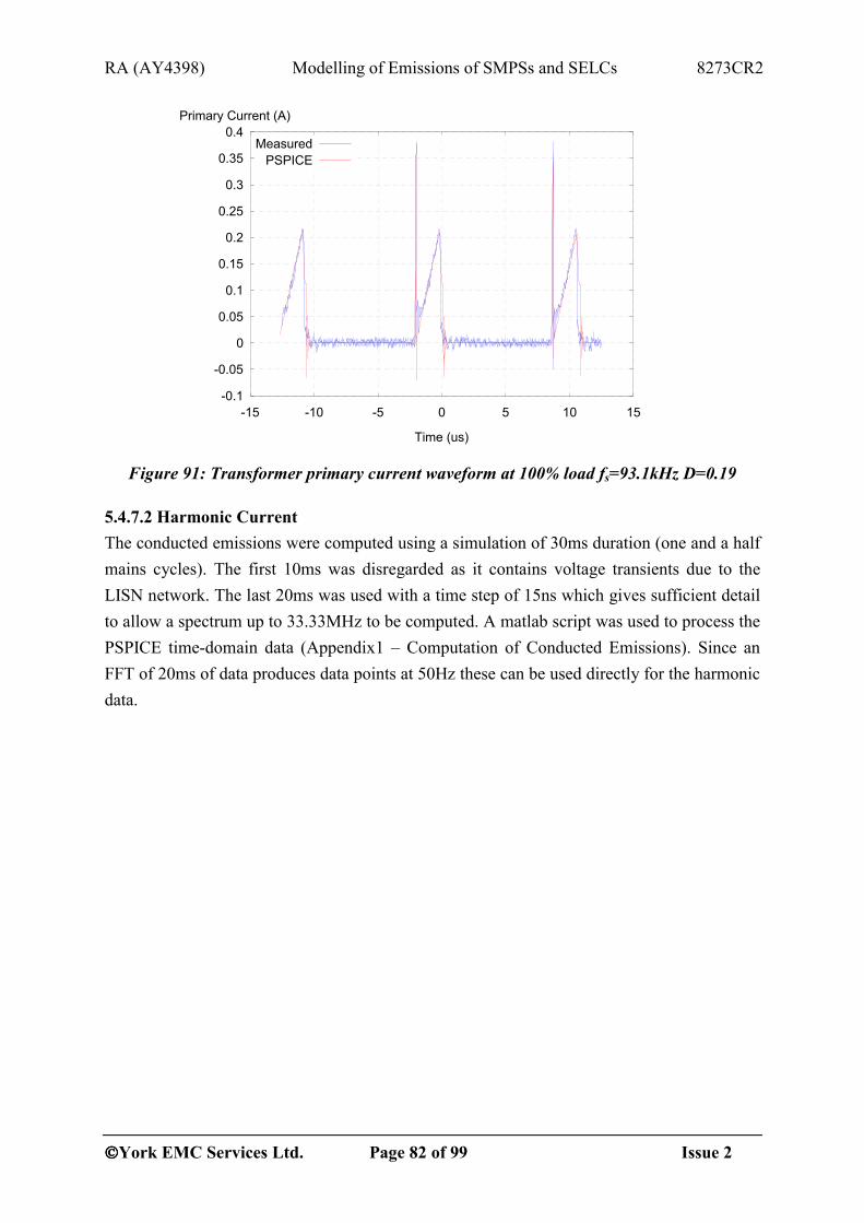
RA (AY4398) Modelling of Emissions of SMPSs and SELCs 8273CR2
York EMC Services Ltd. Page 82 of 99 Issue 2
-0.1
-0.05
0
0.05
0.1
0.15
0.2
0.25
0.3
0.35
0.4
-15 -10 -5 0 5 10 15
Primary Current (A)
Time (us)
MeasuredPSPICE
Figure 91: Transformer primary current waveform at 100% load fs=93.1kHz D=0.19
5.4.7.2 Harmonic Current The conducted emissions were computed using a simulation of 30ms duration (one and a half mains cycles). The first 10ms was disregarded as it contains voltage transients due to the LISN network. The last 20ms was used with a time step of 15ns which gives sufficient detail to allow a spectrum up to 33.33MHz to be computed. A matlab script was used to process the PSPICE time-domain data (Appendix1 – Computation of Conducted Emissions). Since an FFT of 20ms of data produces data points at 50Hz these can be used directly for the harmonic data.
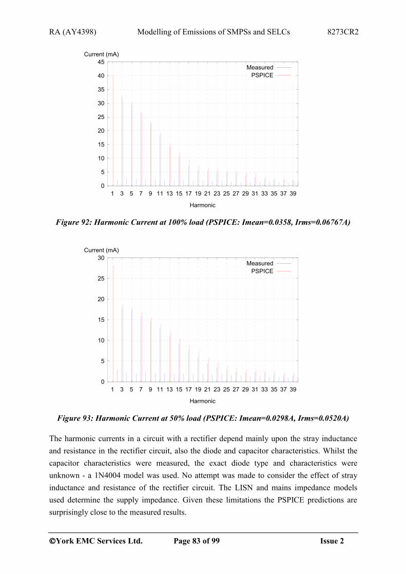
RA (AY4398) Modelling of Emissions of SMPSs and SELCs 8273CR2
York EMC Services Ltd. Page 83 of 99 Issue 2
0
5
10
15
20
25
30
35
40
45
1 3 5 7 9 11 13 15 17 19 21 23 25 27 29 31 33 35 37 39
Current (mA)
Harmonic
MeasuredPSPICE
Figure 92: Harmonic Current at 100% load (PSPICE: Imean=0.0358, Irms=0.06767A)
0
5
10
15
20
25
30
1 3 5 7 9 11 13 15 17 19 21 23 25 27 29 31 33 35 37 39
Current (mA)
Harmonic
MeasuredPSPICE
Figure 93: Harmonic Current at 50% load (PSPICE: Imean=0.0298A, Irms=0.0520A)
The harmonic currents in a circuit with a rectifier depend mainly upon the stray inductance and resistance in the rectifier circuit, also the diode and capacitor characteristics. Whilst the capacitor characteristics were measured, the exact diode type and characteristics were unknown - a 1N4004 model was used. No attempt was made to consider the effect of stray inductance and resistance of the rectifier circuit. The LISN and mains impedance models used determine the supply impedance. Given these limitations the PSPICE predictions are surprisingly close to the measured results.

RA (AY4398) Modelling of Emissions of SMPSs and SELCs 8273CR2
York EMC Services Ltd. Page 84 of 99 Issue 2
5.4.7.3 Conducted Emissions The conducted emissions were computed using a simulation of 30ms duration (one and a half mains cycles). The first 10ms was disregarded as it contains voltage transients due to the LISN network. The last 20ms was used with a time step of 15ns which gives sufficient detail to allow a spectrum up to 33.33MHz to be computed. An octave/matlab script was used to process the PSPICE time-domain data (Appendix1 – Computation of Conducted Emissions). For the conducted data, the power spectrum was averaged over the appropriate bandwidth to obtain the conducted emissions data.
10
20
30
40
50
60
70
80
0.01 0.1 1 10 100
(dBuV)
Frequency (MHz)
Measured L PeakPSPICE L Peak
Quasi-peak LimitMeasurement noise floor
Figure 94: Peak Conducted Interference on the Live terminal at 100% load
Figure 94 shows the measured and peak conducted interference of Item 6 at 100% load. There is again a good correspondence in the structure of the curves and a good correspondence in the amplitude levels from 300kHz to 2MHz. Below 300kHz the amplitude agreement is poor with simulated values exceeding those measured by more than 20dB in places (i.e. at 100 kHz). Above 3MHz the curves diverge with amplitude differences reaching about 10dB. The average levels shown in Figure 95 behave in a similar way.
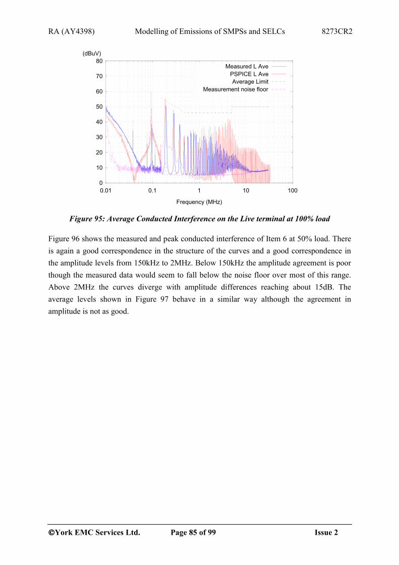
RA (AY4398) Modelling of Emissions of SMPSs and SELCs 8273CR2
York EMC Services Ltd. Page 85 of 99 Issue 2
0
10
20
30
40
50
60
70
80
0.01 0.1 1 10 100
(dBuV)
Frequency (MHz)
Measured L AvePSPICE L AveAverage Limit
Measurement noise floor
Figure 95: Average Conducted Interference on the Live terminal at 100% load
Figure 96 shows the measured and peak conducted interference of Item 6 at 50% load. There is again a good correspondence in the structure of the curves and a good correspondence in the amplitude levels from 150kHz to 2MHz. Below 150kHz the amplitude agreement is poor though the measured data would seem to fall below the noise floor over most of this range. Above 2MHz the curves diverge with amplitude differences reaching about 15dB. The average levels shown in Figure 97 behave in a similar way although the agreement in amplitude is not as good.

RA (AY4398) Modelling of Emissions of SMPSs and SELCs 8273CR2
York EMC Services Ltd. Page 86 of 99 Issue 2
10
20
30
40
50
60
70
80
0.01 0.1 1 10 100
(dBuV)
Frequency (MHz)
Measured L PeakPSPICE L Peak
Quasi-peak LimitMeasurement noise floor
Figure 96: Peak Conducted Interference on the Live terminal at 50% load
0
10
20
30
40
50
60
70
80
0.01 0.1 1 10 100
(dBuV)
Frequency (MHz)
Measured L AvePSPICE L AveAverage Limit
Measurement noise floor
Figure 97: Average Conducted Interference on the Live terminal at 50% load
Figure 98 compares the measured peak interference at 100% and 50% load whilst Figure 99 compares the simulated results. The simulation tracks the behaviour of the measured results in that there is little change in the peak interference levels between 100% and 50% load conditions. The frequencies at which switching harmonics occur agree as the simulation was set to operate at the same frequency as the real supply.

RA (AY4398) Modelling of Emissions of SMPSs and SELCs 8273CR2
York EMC Services Ltd. Page 87 of 99 Issue 2
10
20
30
40
50
60
70
80
0.01 0.1 1 10 100
(dBuV)
Frequency (MHz)
Measured L 100% PeakMeasured L 50% Peak
Quasi-peak LimitMeasurement noise floor
Figure 98: Measured Peak Conducted Interference on the Live terminal
0
10
20
30
40
50
60
70
80
0.01 0.1 1 10 100
(dBuV)
Frequency (MHz)
PSPICE L 100% PeakPSPICE L 50% Peak
Quasi-peak Limit
Figure 99: PSPICE Peak Conducted Interference on the Live terminal

RA (AY4398) Modelling of Emissions of SMPSs and SELCs 8273CR2
York EMC Services Ltd. Page 88 of 99 Issue 2
6 CONCLUSIONS The measurement and estimation of component data to allow the modelling of SMSPSs/SELC has been described and data presented for a phase controller (dimmer switch) and two low-power switched-mode power supplies based on the flyback converter topology.
The operating waveforms of the SMPSs/SELC have been measured and the data used to determine the switching parameters of the models for simulation of harmonic and conducted interference.
Simulations of the three items have been performed, using the PSPICE circuit simulator, at 100% and 50% output power and compared with measurements [1] conducted at a UKAS accredited test laboratory.
6.1 Component measurements and models Measurement of the passive component data was mostly successful and straightforward with the aid of a component bridge and vector network analyser. In most cases, the behaviour could be fitted to the simple models described above with good accuracy. However wound components such as coils, transformers and common-mode chokes, exhibited additional resonances not fully predicted by the simple models.
6.2 Waveform measurements A limited number of waveform measurements were carried out. Primarily to determine the switching point in the phase controller, and the frequency of operation and duty cycle in the flyback converters. Measurements were also used to compare the detailed features of the waveforms in the real devices with the simulation. Here the effect of the measurement probe capacitance and isolation transformer used will have had a significant effect on the measurement and caution must be exercised when examining transient response and rise/fall times.
6.3 Item 7: Rotary dimmer The rotary dimmer was a relatively simple circuit amenable to analytical solution as well as simulation. The phase control circuitry was not simulated, instead a timed pulse voltage source was used to trigger the conduction of the triac – this is not expected to have a significant effect on the harmonic or conducted interference results.
The analytic/semi-analytic and simulation results agree well with the measured data in the case of harmonic currents. This is to be expected as the harmonic content of the waveform depends only on the switching point of the controller, which is easily determined.

RA (AY4398) Modelling of Emissions of SMPSs and SELCs 8273CR2
York EMC Services Ltd. Page 89 of 99 Issue 2
The prediction of conducted emissions depends on accurate knowledge of the performance of the filter components and the switching behaviour (time taken to switch and the shape of the switching waveform) of the triac. The accuracy of the semi-analytic result was as good as the PSPICE simulation. Both failed to predict accurately the measured emissions spectrum. It is clear from the discrepancies between measured and predicted data that insufficient data was available to accurately characterise the triac – for a designer such information may be available in the form of a manufacturers component model or from measurement data. It is also likely that the high current behaviour of the filter choke was not known – all measurements were at low current. Also no attempt was made to model the additional features found in the choke impedance (Figure 10) above 10MHz.
6.4 Items 5 and 6: Flyback converter power supplies The operation of a flyback converter circuit is rather more complex than the phase controller and it was not possible to consider an analytic solution. It was not possible to model the voltage control feedback loop within the power supplies or the detail of the control and switch drive circuitry due to lack of available information – this is not expected to have a significant effect on the harmonic or conducted interference results.
The simulated results agree well with the measured data in the case of harmonic currents. This result should be treated with caution as the current waveform in a rectifier circuit depends critically upon the diode characteristics, stray resistance and inductance in the circuit (including common mode choke and mains impedance), and the reservoir capacitor characteristics. If accurate results are to be obtained all of these must be adequately represented in the model.
The prediction of conducted emissions resulted in poor agreement in the amplitude of the simulated and measured results. The general structure and variation of emissions with load was predicted in the simulations. The level of conducted emissions at high frequencies is very dependent upon the detailed shape and in particular the rise time (first derivative) of the current and voltage waveforms in the switch.
6.5 Modelling harmonic currents in SMPSs/SELCs Overall the modelling of harmonic currents in SMPSs/SELC is feasible and can produce accurate results for phase controlled circuits if the switching phase angle is known. In circuits with rectifiers the currents in the rectifier diodes determines the mains harmonic performance. This can be modelled with good accuracy if the model includes the parasitic elements in the rectifier and reservoir capacitor.

RA (AY4398) Modelling of Emissions of SMPSs and SELCs 8273CR2
York EMC Services Ltd. Page 90 of 99 Issue 2
6.6 Modelling conducted emissions in SMPSs/SELCs The modelling of conducted emissions in SMPSs/SELC depends on the details of the switching waveform (rise-time) and knowledge of the behaviour of the filter components in the circuit. It has been shown that the correct general trends can be seen in the model, but the overall accuracy is poor. More work is required if the reasons for this and sources of inaccuracy are to be discovered. In order to achieve the waveform resolution required to resolve frequency components up to 30Hz a print time-step of 15ns was used resulting in spice output files of over 100MB (30ms simulation) and run times of tens of minutes on a 1.4GHz Pentium processor – a similar time was required for post processing the data.
6.7 Modelling radiated emissions in SMPSs/SELCs In order to predict the currents flowing in this frequency range the waveform detail required would be greater (<0.5ns time step required for operation up to 1GHz). Although the computer performance and disk storage to achieve this is available on modern desk–top computers, the need to measure parasitic elements and model the effects of the physical geometry on the radiation characteristics is likely to make this a more difficult task than that for conducted interference. In particular, the mechanisms driving common-mode currents on the equipment cables would have to be modelled with good accuracy. However if the common mode cable currents were known (e.g. by measurement) the prediction of radiation can be done with a good degree of accuracy as shown by Paul [18, pp412-428].
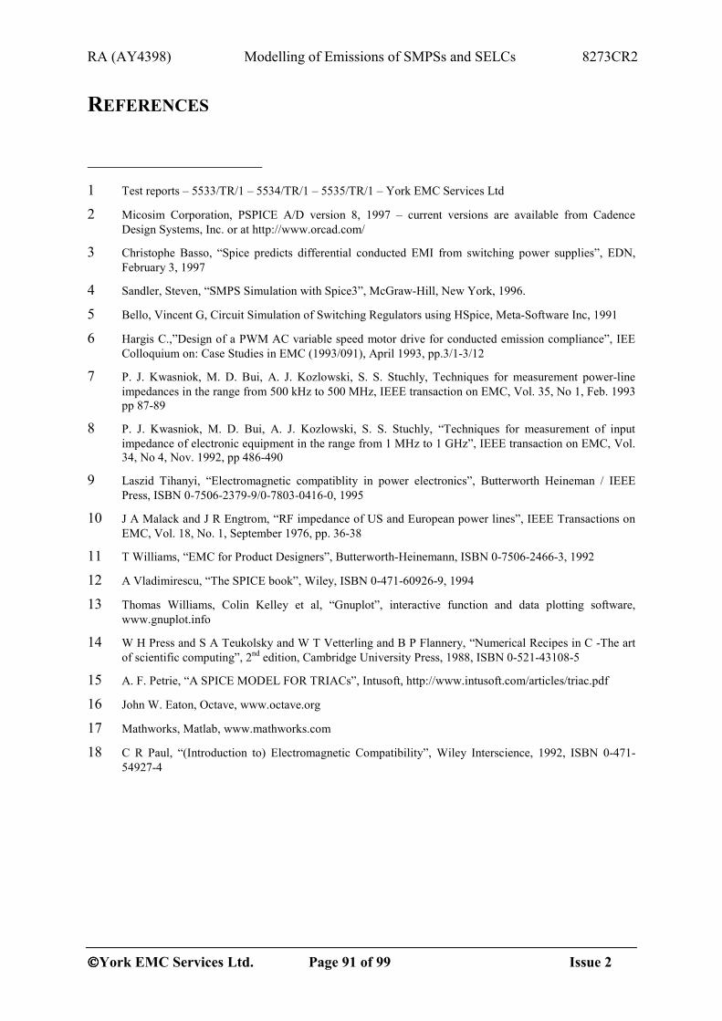
RA (AY4398) Modelling of Emissions of SMPSs and SELCs 8273CR2
York EMC Services Ltd. Page 91 of 99 Issue 2
REFERENCES
1 Test reports – 5533/TR/1 – 5534/TR/1 – 5535/TR/1 – York EMC Services Ltd
2 Micosim Corporation, PSPICE A/D version 8, 1997 – current versions are available from Cadence Design Systems, Inc. or at http://www.orcad.com/
3 Christophe Basso, “Spice predicts differential conducted EMI from switching power supplies”, EDN, February 3, 1997
4 Sandler, Steven, “SMPS Simulation with Spice3”, McGraw-Hill, New York, 1996.
5 Bello, Vincent G, Circuit Simulation of Switching Regulators using HSpice, Meta-Software Inc, 1991
6 Hargis C.,”Design of a PWM AC variable speed motor drive for conducted emission compliance”, IEE Colloquium on: Case Studies in EMC (1993/091), April 1993, pp.3/1-3/12
7 P. J. Kwasniok, M. D. Bui, A. J. Kozlowski, S. S. Stuchly, Techniques for measurement power-line impedances in the range from 500 kHz to 500 MHz, IEEE transaction on EMC, Vol. 35, No 1, Feb. 1993 pp 87-89
8 P. J. Kwasniok, M. D. Bui, A. J. Kozlowski, S. S. Stuchly, “Techniques for measurement of input impedance of electronic equipment in the range from 1 MHz to 1 GHz”, IEEE transaction on EMC, Vol. 34, No 4, Nov. 1992, pp 486-490
9 Laszid Tihanyi, “Electromagnetic compatiblity in power electronics”, Butterworth Heineman / IEEE Press, ISBN 0-7506-2379-9/0-7803-0416-0, 1995
10 J A Malack and J R Engtrom, “RF impedance of US and European power lines”, IEEE Transactions on EMC, Vol. 18, No. 1, September 1976, pp. 36-38
11 T Williams, “EMC for Product Designers”, Butterworth-Heinemann, ISBN 0-7506-2466-3, 1992
12 A Vladimirescu, “The SPICE book”, Wiley, ISBN 0-471-60926-9, 1994
13 Thomas Williams, Colin Kelley et al, “Gnuplot”, interactive function and data plotting software, www.gnuplot.info
14 W H Press and S A Teukolsky and W T Vetterling and B P Flannery, “Numerical Recipes in C -The art of scientific computing”, 2nd edition, Cambridge University Press, 1988, ISBN 0-521-43108-5
15 A. F. Petrie, “A SPICE MODEL FOR TRIACs”, Intusoft, http://www.intusoft.com/articles/triac.pdf
16 John W. Eaton, Octave, www.octave.org
17 Mathworks, Matlab, www.mathworks.com
18 C R Paul, “(Introduction to) Electromagnetic Compatibility”, Wiley Interscience, 1992, ISBN 0-471-54927-4

RA (AY4398) Modelling of Emissions of SMPSs and SELCs 8273CR2
York EMC Services Ltd. Page 92 of 99 Issue 2
APPENDIX 1 COMPUTATION OF CONDUCTED EMISSIONS The following matlab/octave scripts were used to compute harmonic and conducted emissions from the PSPICE time domain output data. The scripts were run under Octave version 2.1.35 but should work with any version of octave – they have not been tested with Matlab but should work with most versions. It may however be necessary to alter the order of the “plot” and “title” statements as octave and Matlab differ here. The time domain data for Live and Neutral conducted interference and line current are read from the input file. The harmonics are simply extracted directly from the FFT of the line current. The conducted interference must emulate the bandwidth of the receiver and the detection process. This is achieved by the following steps:
1. FFT time domain data
2. Select harmonics of interest and multiply by filter characteristic (only a partial spectrum is selected)
3. IFFT of filtered partial spectrum giving complex (I and Q) time domain waveform – this is the complex envelope of the receiver IF
4. Compute peak and average magnitude of complex waveform
5. Save peak, average and centre frequency for later output.
The input file consists of the part of the PSPICE output file containing the time-domain data with its header lines – other data in the output file must be removed.
Dolisnpkavdet – the main program % Read in file of time domain data from LISN and % produce conducted emissions and harmonic spectra %number of harmonics required in the harmonic spectrum nharm=40 %Conducted filter bandwidth (Hz) BW1=0.2e3 BW2=9e3 % Set plot update rate wilst computing plotrate=500 %read in the file: fn=input('file name? ','s'); [t,vlm,vnm,il]=lisnread(fn); %Do the fft with peak and average detection (also harmonics) lisnpkavdet

RA (AY4398) Modelling of Emissions of SMPSs and SELCs 8273CR2
York EMC Services Ltd. Page 93 of 99 Issue 2
lisnpkavdet – process the data %do FFT on lisn data and attempt to compute CISPR Average and Peak %assumes data read elsewhere nin=size(t,2) % set up useful variables dt=t(2)-t(1) % time step nsamp=floor(20e-3/dt) %number of samples in 20ms %select the last 20ms (-1 sample) of simulation - ignore start up transient t=[t(nin-nsamp+1:nin)]; size(t) vlm=[vlm(nin-nsamp+1:nin)]; vnm=[vnm(nin-nsamp+1:nin)]; il=[il(nin-nsamp+1:nin)]; % An attempt to remove the extra 50Hz from vlm %VLM=fft(vlm)*(2/nsamp/sqrt(2)); %vlm=vlm+real(sqrt(2)*VLM(2)*exp(j*w*t)); % compute the mean and RMS line current imean=mean(abs(il)) irms=sqrt(mean(il.**2)) %%%%%%%%%%%%%%%%%% Harmonic Spectrum %%%%%%%%%%%%%%%%%%%%%%%%%%%%%%%%%% %compute the harmonic spectrum % and scale to RMS %IL=abs(fft(il)); %*(2/nsamp/sqrt(2)); IL=(fft(il))*2/nsamp; %truncate the harmonic spectrum IL=[IL(1:nharm)]; %regenerate the waveform from the truncated spectrum tmp=ifft(ifftextend(IL,'even')); ntmp=max(size(tmp)) tmp=tmp*ntmp/2; tt=linspace(0,20e-3*(ntmp-1)/(ntmp),ntmp); %Save it fIL=50:50:50*nharm; %Generate frequency data ff=fopen('harmonic.dat','w'); fprintf(ff,'#Harmonic Spectrum- Imean=%g A, Irms=%g A\n',imean,irms); fprintf(ff,'# Freq (Hz), I(RMS A)\n');

RA (AY4398) Modelling of Emissions of SMPSs and SELCs 8273CR2
York EMC Services Ltd. Page 94 of 99 Issue 2
fprintf(ff,'%g\t%g\n',[fIL;abs(IL)]); fclose(ff); %%%%%%%%%%%%%%%%%% Conducted Spectrum %%%%%%%%%%%%%%%%%%%%%%%%%%%%%%%%%% %compute the conducted spectrum and scale to RMS VLM=fft(vlm)*(2/nsamp/sqrt(2)); VNM=fft(vnm)*(2/nsamp/sqrt(2)); %convert to power spectrum and truncate sM=floor(size(VLM,2)/2); % size of lower half spectrum VLM=VLM(1:sM); %truncate spectrum VNM=VNM(1:sM); %truncate spectrum % Plot the spectra %figure(2) %title('Conducted Spectra'); %semilogx(fNM,10*log10(abs(VLM(1:sM)))+120,fNM,10*log10(abs(VNM(1:sM)))+120); % produce baseband envelope for filtered spectrum % 0.2kHz bandwidth from 9-150kHz % 9kHz BW from 150kHz-30MHz fNM=50:50:50*sM; % Create frequency steps % create the arrays for results - peak, ave, and frequency VLMav=[]; VLMpk=[]; VNMav=[]; VNMpk=[]; fc=[]; i=1; % output index hrbw=floor((BW1/2)/50); % number of elements within BW rbw=hrbw*2+1; % the resolution bw %rspan=hrbw*4+1; % take a span of 2x BW rspan=100+1; % must be odd iffilt=[ones(1,hrbw+1),zeros(1,rspan-rbw),ones(1,hrbw)]; iffilt(hrbw+1)=0.5 ; iffilt(rspan+1-hrbw)=0.5 ; for fk=9e3:BW1/2:150e3 fc(i)=[fk]; % Set frequency jctr=floor((fk)/50)+1; % index to centre freq jmin=floor((fk)/50)-floor(rspan/2)+1; % compute the indices into the big spectrum jmax=floor((fk)/50)+floor(rspan/2)+1; %%%%%%%%%%%% VL - Live %%%%%%%%%%%%%%%%%%%%%% % get the spectral lines into TMP TMP=[VLM(jctr:jmax),VLM(jmin:jctr-1)];

RA (AY4398) Modelling of Emissions of SMPSs and SELCs 8273CR2
York EMC Services Ltd. Page 95 of 99 Issue 2
TMP=TMP.*iffilt; % compute the complex baseband waveform tmp=ifft(TMP)*rspan; % compute mean and peak tmpav=mean(abs(tmp)); tmppk=max(abs(tmp)); % store peak and mean VLMav(i)=tmpav; VLMpk(i)=tmppk; %%%%%%%%%%%% VN - Neutral %%%%%%%%%%%%%%%%%%%%%% % get the spectral lines into TMP TMP=[VNM(jctr:jmax),VNM(jmin:jctr-1)]; TMP=TMP.*iffilt; % compute the complex baseband waveform tmp=ifft(TMP)*rspan; % compute mean and peak tmpav=mean(abs(tmp)); tmppk=max(abs(tmp)); % store peak and mean VNMav(i)=tmpav; VNMpk(i)=tmppk; %%%%%%%%%%%%%%%%%%%%%%%%%%%%%%%%%%%%%%%%%%%%%%%% i++; % next frequency step end hrbw=floor((BW2/2)/50); % number of elements within BW rbw=hrbw*2+1; % the resolution bw %rspan=hrbw*4+1; % take a span of 2x BW rspan=1000+1; % must be odd iffilt=[ones(1,hrbw+1),zeros(1,rspan-rbw),ones(1,hrbw)]; iffilt(hrbw+1)=0.5 ; iffilt(rspan+1-hrbw)=0.5 ; for fk=150e3:BW2/2:fNM(size(fNM,2)-(rspan-1)/2) fc(i)=[fk]; % Set frequency jctr=floor((fk)/50)+1; % index to centre freq

RA (AY4398) Modelling of Emissions of SMPSs and SELCs 8273CR2
York EMC Services Ltd. Page 96 of 99 Issue 2
jmin=floor((fk)/50)-floor(rspan/2)+1; % compute the indices into the big spectrum jmax=floor((fk)/50)+floor(rspan/2)+1; %%%%%%%%%%%% VL - Live %%%%%%%%%%%%%%%%%%%%%% % get the spectral lines into TMP TMP=[VLM(jctr:jmax),VLM(jmin:jctr-1)]; TMP=TMP.*iffilt; % compute the complex baseband waveform tmp=ifft(TMP)*rspan; % compute mean and peak tmpav=mean(abs(tmp)); tmppk=max(abs(tmp)); % store peak and mean VLMav(i)=tmpav; VLMpk(i)=tmppk; %%%%%%%%%%%% VN - Neutral %%%%%%%%%%%%%%%%%%%%%% % get the spectral lines into TMP TMP=[VNM(jctr:jmax),VNM(jmin:jctr-1)]; TMP=TMP.*iffilt; % compute the complex baseband waveform tmp=ifft(TMP)*rspan; % compute mean and peak tmpav=mean(abs(tmp)); tmppk=max(abs(tmp)); % store peak and mean VNMav(i)=tmpav; VNMpk(i)=tmppk; %%%%%%%%%%%%%%%%%%%%%%%%%%%%%%%%%%%%%%%%%%%%%%%% i++; % next frequency step end %Save the averaged data ff=fopen('conductedrx.dat','w'); fprintf(ff,'#Conducted Interference Spectrum\n'); fprintf(ff,'# Freq (Hz), VLpk (VRMS), VLav (VRMS), VNpk (VRMS), VNav (VRMS)\n');

RA (AY4398) Modelling of Emissions of SMPSs and SELCs 8273CR2
York EMC Services Ltd. Page 97 of 99 Issue 2
fprintf(ff,'%g\t%g\t%g\t%g\t%g\n',[fc';abs(VLMpk)';abs(VLMav)';abs(VNMpk)';abs(VNMav)']); fclose(ff);
ifftextend – compute the conjugate image of a spectrum prior to ifft function v = ifftextend (t,odd) %extend a frequency response to add complex conjugate part for IFFT % We must either produce the conjugate of t(2:N) giving an odd number of elements % or let t(N) become real and add the conjugate of t(2:N-1) which % produces an even array. % expects a vector... %Copy array as is into first part v=t; %default to odd if (nargin==1) odd='odd'; end %make conjugate part if strcmp(odd,'odd') k=max(size(t)); n=1; for i=k:-1:2 v(k+n)=conj(t(i)); n=n+1; end else k=max(size(t)); n=1; for i=k-1:-1:2 v(k+n)=conj(t(i)); n=n+1; end v(k)=real(v(k)); % the 'middle' element must be real end end

RA (AY4398) Modelling of Emissions of SMPSs and SELCs 8273CR2
York EMC Services Ltd. Page 98 of 99 Issue 2
APPENDIX 2 PHASE CONTROL WAVEFORM GENERATION The following matlab/octave scripts used to compute the ideal time-domain waveforms for the rotary dimmer. The scripts were run under Octave version 2.1.35 but should work with any version of octave – they have not been tested with Matlab but should work with most versions. It may however be necessary to alter the order of the “plot” and “title” statements as octave and Matlab differ here. The waveform is generated by the following steps:
1. Generate 30 ms (1½ cycles) the modulating unit square wave ;
2. Convolve modulating square wave with pulse equal in width to rise time, giving a trapeziodal waveform;
3. Multiply the trapezoidal waveform with the sinusoidal waveform and scale for current and conducted interference waveforms in separate arrays ready for processing by lisnpkavdet or similar..
4. Save the time domain waveforms
The waveform parameters are defined as constants in the file.
Testlisnfft_pc – generate phase control waveforms %Test the LISN FFT code with a basic Phase control waveform %set the lisnfft parameters %number of harmonics required in the harmonic spectrum nharm=40 %Conducted filter bandwidth (Hz) BW1=0.2e3 BW2=9e3 % Set plot update rate wilst computing plotrate=500 %Set the waveform parameters dt=15e-9 % 15ns timestep is used in the PSPICE simulations %dt=0.5e-6 % a 0.5us time step takes us to 1MHz - faster for testing %dt=1e-3 % a 0.1ms timestep is much faster for code testing... tmax=30e-3 % 30ms of simulation is used in the PSPICE simulations % The first 10ms is discarded phideg=80 % Switching angle (0-180 deg) % 80degrees corresponds to "half power" simulation % Rise time of switching waveform %trise=0.0 %trise=0.5e-6 %trise=1.0e-6 %trise=2.0e-6 trise=3.0e-6
RA (AY4398) Modelling of Emissions of SMPSs and SELCs 8273CR2
York EMC Services Ltd. Page 99 of 99 Issue 2
%trise=4.0e-6 %trise=8.0e-6 f=50 % Mains frequency w=2*pi*f % ANgular frequency Vpk=325 % Peak voltage of supply RL=210 % Load resistance %Create the waveform and time axes nin=floor(tmax/dt) %Number of samples cycles=tmax*f ncycle=floor(1/(f*dt)) t=linspace(0,tmax-dt,nin); %time steps %generate switch waveform %first half cycle tmp=[zeros(1,floor(phideg/360/f/dt+0.5)),ones(1,ncycle/2-floor(phideg/360/f/dt+0.5))]; tmp; %remaining half cycles for i=1:0.5:cycles tmp=[tmp,tmp]; end tmp=tmp(1:nin); %truncate to correct length (above may add elements) %Add in rise time - convolve with rise pulse if (trise>0.0) hnrise=floor((nin-1)*trise/tmax/2)+1 tmp=real(ifft(fft(tmp).*fft([ones(1,hnrise),zeros(1,nin-2*hnrise),ones(1,hnrise)]).^2)).*1/(2*hnrise).^2; end %let vnm stand as switching waveform %generate the full waveform in il vlm, vnm il=tmp.*sin(w*t)*Vpk/RL; % a pure sine wave vlm=50*il*RL/(RL+100); %Live and Neutral voltages for ideal LISN vnm=-vlm; % Plot the current waveform figure(4) %plot(t,vnm,t,vlm) title('Current and modulating square-wave'); plot(t(1:10:nin),tmp(1:10:nin),t(1:10:nin),il(1:10:nin)) %decimate to speed plot %Save the decimated time-domain waveform ff=fopen('pc_td.dat','w'); fprintf(ff,'#Time domain waveforms from testlisnfft_pc.m\n'); fprintf(ff,'# Time (s), VL (V), VN (V), IL(A), P\n'); fprintf(ff,'%g\t%g\t%g\t%g\t%g\n',[t(1:100:nin);vlm(1:100:nin);vnm(1:100:nin);il(1:100:nin);tmp(1:100:nin)]); fclose(ff);


