Radiation Hardness Assessment of MR sensors for Space Applications Pedro Alves pedrofl[email protected]Instituto Superior T´ ecnico, Lisboa, Portugal November 2017 Abstract As we all might know, doing space exploration is not cheap. Two factors which have a major impact on a space missions budget are related to the mass and the power consumption associated with a spacecraft. So, when we speak about any device which deals with the sensing of a magnetic field in order to perform some function, it is not acceptable not to consider magnetoresistive technology. Magnetoresistive sensors have a huge potential for space applications due to their reduced dimensions, power consumption, and the wide range of applicability. Nevertheless, one of the facts why they are still not being intensively applied, for example in magnetometers or other applications, has to do with the lack of data about radiation effects on them, among other challenges. In this work, different type of magnetoresistive sensors (spin valves, and magnetic tunnel junctions with MgO and AlOx barriers) were irradiated up to a total ionizing dose of ∼ 5 Mrad with gamma radiation. This experiment had the objective to assess the behaviour of these sensors by inspecting if modifications induced by gamma radiation would appear or not in their characteristic parameters like transfer curve, saturated states, output signals, coercivity, transfer curve offset, and sensitivity. The irradiation was done in three steps and during these periods the sensors were unbiased. After each irradiation step, the sensors were remotely characterised. The results have shown practically no sign of degradation of the sensors’ parameters keeping, then, their performance intact. Keywords: Magnetoresistance, Magnetoresistive sensors, Gamma irradiation, Rad-hard , Total ionizing dose Contents 1 Introduction 2 2 Background 2 Magnetoresistance effect ...................................... 2 Space radiation environment ................................... 2 3 Sensors fabrication 3 4 Characterisation method and irradiation experiment 4 5 Results 5 Measurement conditions ...................................... 5 Transfer curves ............................................ 5 Saturated states ........................................... 5 MR signal and WB output difference ............................. 6 Coercivity ............................................... 6 Transfer curve offset ........................................ 6 Sensitivity ............................................... 6 6 Conclusion 8 1
Transcript
Radiation Hardness Assessment of MR sensors for Space
As we all might know, doing space exploration is not cheap. Two factors which have a majorimpact on a space missions budget are related to the mass and the power consumption associated witha spacecraft. So, when we speak about any device which deals with the sensing of a magnetic fieldin order to perform some function, it is not acceptable not to consider magnetoresistive technology.Magnetoresistive sensors have a huge potential for space applications due to their reduced dimensions,power consumption, and the wide range of applicability. Nevertheless, one of the facts why they arestill not being intensively applied, for example in magnetometers or other applications, has to do withthe lack of data about radiation effects on them, among other challenges. In this work, different typeof magnetoresistive sensors (spin valves, and magnetic tunnel junctions with MgO and AlOx barriers)were irradiated up to a total ionizing dose of ∼ 5 Mrad with gamma radiation. This experiment hadthe objective to assess the behaviour of these sensors by inspecting if modifications induced by gammaradiation would appear or not in their characteristic parameters like transfer curve, saturated states,output signals, coercivity, transfer curve offset, and sensitivity. The irradiation was done in threesteps and during these periods the sensors were unbiased. After each irradiation step, the sensorswere remotely characterised. The results have shown practically no sign of degradation of the sensors’parameters keeping, then, their performance intact.
Nowadays, space and planetary assessment arestarting to be supported by smaller spacecraft. Themain reason for this is to lower down the costs as-sociated with a mission. One way of doing thatis through the reduction of the size and energyconsumption of the components which constitutea spacecraft. Another alternative and complemen-tary strategy is, instead to use highly qualified butexpensive components in space applications, to usecommercial generic ones. These have the benefitsof being cheaper, to have easier access to them,lower delivery times, and the fact that their perfor-mance is not so low when compared with the onesassociated with qualified components. Neverthe-less, the drawback of using these components as todo with the lack of information about their behav-ior against the harsh environment of space. Whenwe talk about magnetic sensors for space applica-tions, magnetoresistance technology is naturally anoption due to their features small sizes, low powerconsumptions and their wide range of applicability.Though, some of the magnetoresistive (MR) sensorsare not yet totally mature and ready to be used inspace (e.g. Magnetic tunnel junction sensors).
Other aspect why MR sensors are so desired tobe used for space applications, are the fact thatit is known that they present a good tolerance toradiation. In the beginning of 2000, Guo et al.(2001) [1] did the irradiation of SVs, composed byIrMn/CoFe/Cu/CoFe/NiFe , with 30 keV Ga+2 andobserved a decrease of exchange bias and MR sig-nal, as also the increment of resistance with theincrease of ion doses. Carroll (2010) [2] shown thatSVs ((Si / SiO2 3000/ Ni80Fe20 100 / Cu 61 /Ni80Fe20 100 / Fe50Mn50 200 / Ge 100 , thickness inangstroms) kept their functionality, though, smallchanges (variations of 4 and 6 Oe were observed)in coercivity and a decrease trend of the MR signal(overall decreases of 0,15 to 0,44 % were noticed)were verified while exchange bias was observed tobe rad hard, after gamma irradiations up to a doseof 50 Mrad. Conraux et al. (2003) [3] presented re-sults from the bombardment of AlOx-based MTJswith high energetic (10 MeV/A) heavy ions, wherean irreversibly small decrease in TMR amplitudewith the increase of ion fluence was observed. Avery good review article on radiation effect of MRsensors was presented by Lu et al. (2014) [4], whereAMR sensors displayed in a Wheatstone configura-tion, appeared to be resistant to irradiation withgamma rays for values of TID until 200 krad. Inother study [5] from the analysis of TID effects of200 krad in AMR sensors in Wheatstone bridge con-figuration, it was shown that the sensors only suf-fered small performance degradation (with errorsfor the sensing field lower than 10 nT). In order to
evaluated TID effects on MR sensors, biased singleMgO-based MTJs were exposed to doses of gammaradiation up to 10 Mrad [6]. No signs of device’sperformance modifications, neither in terms of itsmagnetic (coercivity and TMR signal) and electricproperties, were observed. Still on the evaluationof TID effects, Arias et al. (2015) [7] have irradi-ated MgO-based MTJs current sensors configuredin a Full Wheatstone bridge with X-rays up to adose of 43 krad. They noticed that neither the MRsignal nor bridge resistance were affected. Never-theless, during irradiation, sensitivity and hystere-sis suffered small decreases. Sensitivity was recov-ered, while hysteresis has reached higher values ina post-irradiation period.
To start, a brief introduction of the magnetore-sistive phenomena and the space radiation environ-ment and its effects will be presented. Next, thethree types of magnetoresistive sensors which wereevaluated will be identified. Also, the fabricationprocess of one of the types will be mentioned. Then,the method by which the sensors were characterisa-tions and the irradiation experiment are introduced.After knowing the methodology, the results of theirradiation will be presented and discussed. In theend, some conclusions are made.
2. Background
Magnetoresistance effect
Magnetoresistance (MR) effect may be defined asthe change of an electrical resistance, when a cur-rent flow through a material, due to the applicationof a magnetic field, R = f(H). According to themechanism behind MR phenomenon, it is possibleto categorise them in three main types: anisotropic[8], giant [9], and tunnel magnetoresistance effect[10]. One common parameter to all of MR mecha-nisms is the MR signal, which may be quantified asthe maximum variation of the resistance, and canbe represented in the following ratio form:
MR(%) =Rmax −Rmin
Rmin× 100. (1)
Depending on the type and requirements of an ap-plication, one of the three MR’s mechanisms men-tioned above is typically among the elected choice.On the Table 1 it is shown some of the main fea-tures of the sensors employing the different kind ofMR mechanisms. MR effect has been extensivelyused for a while in magnetic recording, magneticfield sensors, non-volatile memories, among manyothers.
Space radiation environment
It is important to know very well what will bethe radiation environment that some components or
2
Table 1: Key features of sensors implementing MR effect. Adapted from: [11, 12]
AMR GMR - Spinvalves (SV) TMR - Magnetic tunnel junctions (MTJ)Physical principle Anisotropic MR Giant MR Spin dependent tunneling
Thin film structure SimpleBuffer/free/cap
Multilayers composed by diverse materialsBuffer/pinning/reference/spacer/free/cap
Complex multilayers composed by diverse materialsBuffer/pinning/reference/barrier/free/cap
Thermal stability up to 250 C up to 320 C up to 360 CSensor linear range (Oe) 1 - 100 10 - 50 20 - 100
Magnetic anneal treatment (C) not required ∼ 250 ∼ 350Electrostatic discharge protection (robustness) very good good fair
Materials cost cheap expensive expensive
even Humans will be subjected, for example, dur-ing the execution of a space mission. The radiationissues are considered one of the most dangerous haz-ards found in space. Space radiation may be cat-egorized, mainly, by three types according to theirorigin: cosmic galactic rays (CGRs), solar parti-cle events (SPE), and particles trapped in radiationbelts.
Figure 1: Main sources of radiation found in space.From: NASA
• Space radiation sources
GCRs are mainly composed of charged particleswhere 98% are protons and heavier ions. The re-main 2% are electrons and positrons. GCRs arevery well known for having the highest energies inthe cosmos. Within our solar system, they can havesome tens of MeV up to 1012 MeV. Comparativelywith the other two sources, GCRs are also knownby having the lowest flux of particles. An importantaspect of GCRs fluxes is that they are modulatedby the solar activity.
Solar particles like electrons, protons, and heavierions (from He to U) can be found anywhere in theinterplanetary space and may present energies from10 till 102 MeV. These particles may be producedby two types of solar events namely Solar Flares(SFs) and Coronal Mass Ejections (CMEs). Thistype of radiation affects predominantly missions athigh planetary orbits as well as missions outer of
space since there is no natural magnetic shieldingout there.
Around the Earth, at altitudes from 100 to 104
of kilometres, there are two separated main regionswhere numerous electrons and protons are confinedwithin the geomagnetic field lines, as we can see inthe Figure 1. These regions are known as the VanAllan radiation belts. The electrons and protonsthat reside in these regions can have energies from∼ 0.1 to 10 MeV and ∼ 0.1 up to 103 MeV, re-spectively. In the slot region, which separates thetwo belts, plasma populations with energies smallerthan 0.1 MeV may be found.
• Space radiation effects
Depending on diverse factors associated toradiation-matter interaction (as radiation source,energy, dose, and materials features like latticeatoms organization, composition and grain size),different mechanisms may occur leading to the ap-pearing of different effects. Radiations interactionsmay be pronounced mainly through the followingeffects: total ionizing dose effects (TID), displace-ment damage (DD), single event effects (SEE), andelectrostatic discharges (ESDs).
TID was assessed within this project. This, rep-resents the effects associated with the accumulateddose of ionizing radiation deposited in some mate-rial. So, TID can be seen as the long-term effect ofradiation, being also possible to infer the amountsof ionizing doses for which a device may withstand.This type of assessment can be done by subjectingmaterials to a Cobalt-60 source which are consid-ered a standard radiation source for testing.
3. Sensors fabrication
Magnetic tunnel junctions with AlOx barrier werefabricated from the scratch in order to assess thegamma radiation effects on then.
Six main processes were done in order to havethe final sensor. First, a two deposition step processwith the same MTJ stack (Ta 50 / [Ru 150/ Ta50]x3/ NiFe 30 / CoFeB 30 / Al 8 (Ox 30”) / CoFeB 30/Ru 6 / NiFe 30 / MnIr 180 / Ru 150 / Ta 50 ,where the numbers represent the thickness of eachlayer given in angstroms) was done. The e.a. (easy
3
axis) of the stack deposited in the second step wasrotated about 180 relatively to the e.a. of the firststack. This strategy allowed the fabrication of fullWheatstone bridge. The deposition was done inan ion beam system (Nordiko 3000). After havingthe stacks deposited on top of the substrate (Si /SiO2 1000), the bottom electrodes were patternedby photolithography technique implemented by adirect write laser system (DWL), and then definedby an ion milling process (in Nordiko 3000).
Figure 2: Bottom electrode and MTJ pillar features.
Next, the main part of the sensor (MTJ pillar)was defined. The pillar was defined with dimen-sions of 2 µm by 40 µm. After the ion milling ofthe pillars, a passivation of 1214 A with aluminawas performed by a RF magnetron sputtering sys-tem (UHV2). After passivation was finished, a lift-off process was done (8 hours duration) in order touncover the MTJ pillars from the photoresist layerwhich patterned the pillars and protect them fromthe ion milling process. After this, the top elec-trodes were patterned and a thick layer of AlSiCu(1,2 µm) plus a TiWN2 were deposited in a mag-netron sputtering system (Nordiko 7000). The lastprocess of fabrication was to open vias (through alift-off process) to the contact pads in order to ac-cess to the sensors, after a final passivation of 1500A of alumina.
After fabrication, the sensors were implementedon chip-carriers, as we observe in Figure 3.
Figure 3: Chip-carrier with one of the fabricated chipimplemented on it. (circle) Wirebonding.
4. Characterisation method and irradiationexperiment
• Sensors characterisation
After finishing the fabrication of the sensors, Iproceeded to their characterisation. Two moretypes of MR sensors, spin valves and MgO-basedMTJs, were also characterised and subjected to therest of the experiment. Parameters like output sig-nal, saturated resistance, coercivity, effective cou-pling field were obtained. These parameters wereobtained from their magnetotransport curves whichwere measured by using a manual setup - 140 Oesetup. The varying magnetic field is created by thechange of intensity and direction (±4 A) of a cur-rent, generated by a bipolar DC current source sys-tem (Kepco), flowing through two Helmholtz coils.For the characterisations of the sensors, we shouldbias first then with a current (power source) or avoltage (sourcemeter), depending on the configu-ration of the sensors. When the application of thevarying field is turn on, for each point of it, a poten-tial difference is measured with a multimeter. Allthe three instruments are connected to a computer,through a GIPB connection in order to display theobtained data.
Before the implementation of the sensors on thechip-carriers, they were biased and measured witha two or four probes, composed by tungsten needlesin their extremities, moved by micropositioners. Af-ter implementation, sensors characterisations werecarried on in a proper chip-carrier connector linkedto a pins selector board.
All of the sensor characterisations were done atINESC-MN facility in Lisbon.
• Irradiation experiment
In order predict how the magnetoresistive sensorswould behave in space environment, inspections ofthe radiation effects on their performance were donethrough an irradiation experiment.
The irradiation was done with gamma radiationresulting from the decay of a Cobalt-60 source, witha half time of ∼ 5 years. Gamma radiation is knownby being one of the most penetrating and energeticelectromagnetic radiation. Irradiation tests usingthis kind of sources for inspections of the long-termeffects of ionizing doses and qualification of com-ponents are very frequent, since represents a worst-case scenario, for example, in the case if the compo-nents were supposed to be launched in a spacecraftto space.
The sensors were exposed to radiations with ener-gies between ∼ 1.1 and ∼ 1.3 MeV. The irradiationwas performed up to a total ionizing dose of ∼ 5MRad (50 kGy). This dose was delivered to thesensors in three steps of ∼ 1h. In order to reach
4
the desired level of interest, the sensors were posi-tioned in a specific slot with a specific distance fromthe source of Co-60 with a dose rate of ∼ 1.688MRad/h (16.88 kGy/h). During the irradiations,the sensors were always unbiased. In order to in-spect if some changes would appear or not along theirradiations, once an irradiation step was finishedthe sensors were taken to INESC-MN in order tobe (remotely) characterised. Still, during irradia-tions, sensors were irradiated unbiased. A group ofsensors were not irradiated, nevertheless, they alsosuffered from the same handling and external con-ditions (except the irradiation) which the irradiatedones suffered (e.g. transport between facilities). So,during the irradiation experiment, the sensors werecharacterised in three different periods: before irra-diations, between irradiation steps (done after eachstep), and after irradiations. The characterisationsfor each period were done in different days.
The irradiations took place at the TechnologicalUnit of Radiosterilization at Campus Tecnolgico eNuclear - Instituto Superior Tcnico (CTN-IST) -Sacavm.
5. Results
Rightly after the fabrication process, described onthe section 3, characterisations were performed outof the chip-carrier and in. These first characterisa-tions were essential in order to make it possible thecomparison between the initial state of the sensorto its response after some stage of irradiation.
Measurement conditions
Different initial conditions were used for each typeof sensor during the measurements. Bias currentsof 1 mA, 1,5 mA were applied to the individualSV sensors, series of MTJs with MgO barrier, re-spectively. On the other hand, the full Wheatstonebridge constituted with AlOx-based MTJs was biaswith a constant voltage of 1,5 V with the sourceme-ter.
About the software parameters, the data were ob-tained for a range of magnetic field between -141to 141 Oe. Inside of this interval, different varia-tion steps (in Oe) of the field were used: 20, 4,2,1.The dependent parameter, was measured 5 timesfor each value of the field. These points were takenafter 0,5 s of the stabilization of the field.
Transfer curves, saturated levels, coercivities,and sensitivity were some of the evaluated parame-ters.
Transfer curves
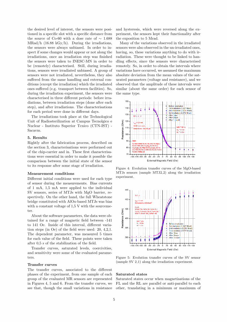
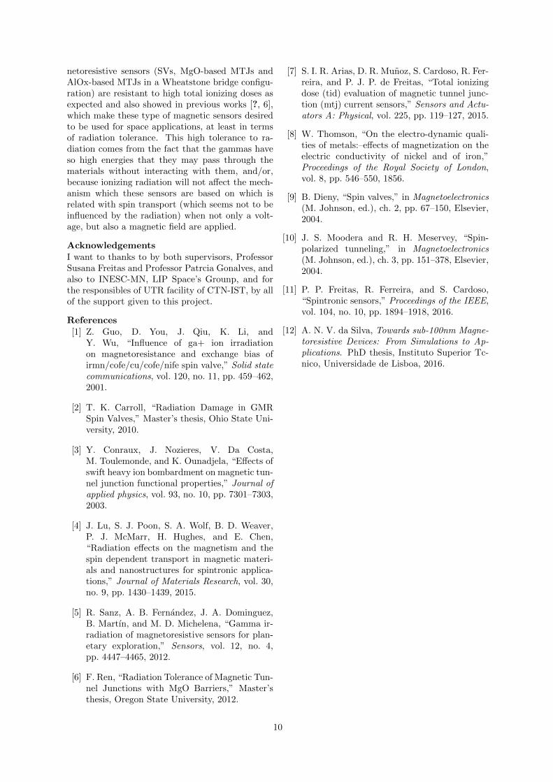
The transfer curves, associated to the differentphases of the experiment, from one sample of eachgroup of the evaluated MR sensors are representedin Figures 4, 5 and 6. From the transfer curves, wesee that, though the small variations in resistance
and hysteresis, which were reversed along the ex-periment, the sensors kept their functionality afterthe exposition to 5 Mrad.
Many of the variations observed in the irradiatedsensors were also observed in the un-irradiated ones,having, so, these variations anything to do with ir-radiation. These were thought to be linked to han-dling effects, since the sensors were characterisedremotely. So, in order to obtain the intervals wherevariations have occurred, we assumed the maximumabsolute deviation from the mean values of the sat-urated parameters (voltage and resistance), and weobserved that the amplitude of these intervals weresimilar (about the same order) for each sensor ofthe same type.
Figure 4: Evolution transfer curves of the MgO-basedMTJs sensors (sample MTJ2 2) along the irradiationexperiment.
Figure 5: Evolution transfer curves of the SV sensor(sample SV 2 1) along the irradiation experiment.
Saturated statesSaturated states occur when magnetisations of theFL and the RL are parallel or anti-parallel to eachother, translating in a minimum or maximum of
5
Figure 6: Evolution transfer curves of the WB sensor(sample WB 10) along the irradiation experiment.
electrical resistance identified by the plateaus in thetransport curves. The saturated states of the sen-sors are presented in Figures 7, 8, and 9. From theinspection of these we observe that:
• for the tree type of sensors evaluated, we seethat the parameters correspondent to the sat-urated states, resistance for the SVs and seriesof MgO-based MTJs, vary practically withinthe same interval (band) used to account forthe handling effects, with maximum absolutedeviations about their mean values of Rp andRap about: ∼ 2 and ∼ 1,5 Ω, ∼ 0,3 and ∼0,8 Ω, respectively. These variations are < 1% relative to the respective Rp and Rap meanvalues;
• for the irradiated WBs we noticed that the in-tervals were variations have occurred along theexperiment was insignificant compared withthe one associated to the un-irradiated samplewhich had a maximum absolute deviation of ∼6 mV for the Vmax and Vmin, considering, so,variations in the irradiated samples (one orderbellow) insignificant;
• for the sample MTJ 2 2 we noticed a distin-guishable superior value of Rap for the 3rd ir-radiation phase relative to the values in otherphases. Nevertheless, after this phase, the re-sistance has decreased and remained at thesame level during the remain characterisations.This bump in resistance was not verified in anyother MTJ sample.
MR signal and WB output differenceThe output signals of the sensors were also evalu-ated and are given by the MR ratios of the MTJsand SVs, and by the output difference of the WBs,presented in Figures 10, 11, and 12. Using the sametreatment done as before in order to account the
effects of handling for the resistances, an intervalwhere the values for the output signals of the ir-radiated sensors may vary was obtained. Again,in order to obtain the interval where variations oc-curred, the maximum absolute deviation relative tothe mean value of the output signal for each samplewas used.
Like for the saturated states, as we expected, theinterval where MR signal variations for the irradi-ated sensors occurred are practically the same as-sociated to the one observed for the un-irradiatedsample, as we may see in the Figures 10 and 11.
Coercivity
Coercivity of a sensors can be defined as the hys-teretic behaviour close to zero field. The MgO-based MTJ and SV irradiated sensors presented,practically, no coercivity. For the WBs we saw thatsome 1,5 Oe variations for the WB 1 and 13, as wecan see in Figure 13. Nevertheless, for the threeevaluated sensors no trend associated to irradia-tion was verified, what suggest us that, probably,these variations are not related with irradiations,but maybe with some intrinsic behaviour.
Transfer curve offset
The curves offset relative to zero field (which corre-sponds to the field of the middle-point of a curve)was another evaluated parameter and the results arepresented in Figures 14. Shifts in transfer curvesmay result from an effective coupling field conse-quence from the interactions between the magneticlayers, like, ferromagnetic Nel coupling between theFM layers separated by a spacer (FM / spacer /FM) induced from interface interactions, the cou-pling of the demagnetizing field of both FM layers,and the exchange bias coupling across the spacer de-scribed by RKKY-theory (where depending on thespacer thickness a ferromagnetic/antiferromagneticexchange bias coupling between the FM layers mayoccur).
From the inspection of this parameter, we mayalso consider that gamma irradiation did not haveany relevant effect, since the variations occurred inthe irradiated samples have practically the samemagnitude as the uncertainty associated to the field(0,5 Oe for the 1 Oe step field).
Sensitivity
In order to evaluate the sensitivity of the sensors,linear fittings of the transfer curves in a region closeto zero field (field range between -10 Oe to 10 Oe)where the data were more precisely obtained (withfield steps of 1 Oe) were done. Sensitivities are pre-sented in Figures 15, 16, and 17, and they reflectthe rotation of the free layer as the field is changing.The sensitivities were obtained for the two direc-tions which the field varied, and are denominated
6
Figure 7: Evolution of the saturated states, parallel (Rp) and anti-parallel (Rap) resistances for the MgO-basedMTJs (un-irradiated MTJ, MTJ 2 2 and 2 3) along the irradiation stages. The band represented in each graphrepresents the interval where variations were observed. These intervals have in consideration the maximumabsolute deviations relative to the mean value of Rp and Rap, where, for the MgO-based MTJs, maximumdeviations of ∼ 0,3 and ∼ 0,8 Ω were, respectively, obtained.
Figure 8: Evolution of the saturated states, parallel (Rp) and anti-parallel (Rap) resistances for the SVs (un-irradiated SV, SV 2 1 and 2 3) along the irradiation stages. The band represented in each graph represents theinterval where variations were observed. These intervals were considered to be the maximum absolute deviationrelative to the mean value of each sample. For the SVs, the intervals where variations are observed, are associatedto maximum absolute deviations of ∼ 2 and ∼ 1,5 Ω relative to Rp and Rap mean values, respectively.
Figure 9: Evolution of the saturated voltages, Vmin and Vmax, for the WBs (un-irradiated WB, WB 10 and13) along the irradiation stages. For the WBs the variations of the irradiated where considered insignificant (oneorder below) when compared with the ones verified for the un-irradiated sensor ∼ 6 mV for the Vmax and Vmin.
by up and down.
For sensitivity, the results practically do not showany significant variations or trend indicative of irra-diations effects. The small variations observed (ofthe order of 0,01 mV/Oe) are due other externalfactors like the handling of the sensors.
Here, we used the standard errors from the fits asthe uncertainty for each sensitivity. We notice, fromthe figures with the sensitivities, that along the ir-
radiation experiment there are some values that areno inserted in the uncertainties of the remains sen-sitivities. Nevertheless, since no significant varia-tions, as well as any trend associated to a possiblevision of radiation effects, were observed during theexperiment, it suggested that maybe other exter-nal factor had affected may have caused the smalldeviations observed in the sensitivities.
7
Figure 10: Evolution of the MR signal associated to the MgO-based MTJs along the irradiation stages. Thebands represented the interval where the variations occurred. For this case, these intervals bands are associatedto a maximum absolute deviations close to ∼ 1,1 %.
Figure 11: Evolution of the MR signal for the SVs along the irradiation stages. For the SVs the intervals wherevariations were observed, are associated to maximum absolute deviations close to ∼ 0,1 %.
Figure 12: Evolution of the output signal, ∆V0 = Vmax − Vmin, for the WBs along the irradiation stages.
Figure 13: Coercivity evolution for the WBs (un-irradiated WB, WB 1, 10 and 13) along the irradiationstages.
6. ConclusionFrom the analysis of the data presented in section5, no tested sample was found to suffer any relevant
degradation due to irradiation with 60Co gammas.The sensors kept their global performance intact,like we observed in the transfer curves, during theirradiation experiment. Some of these curves haveshown some changes, like variations of resistanceand, also, the appearance of the hysteresis-like be-haviour. Nevertheless, these changes were reversed.About the origin of these changes, it was concludethat they did not have anything to do with the ir-radiation since:
• through the inspection of the magneto-transport and sensor parameters (coercivity,curve offset, MR signal, saturated states, andsensitivity) we observed that, for the threetypes of evaluated sensors, though some of thethem had felt small variations, no explicit trendshowing any sign of potential gamma irradia-tion damage during the characterisations wasobserved neither within each group of sensorsnor among the four types;
8
Figure 14: Evolution of the transfer curve offset for (left) MgO-based MTJs, (middle) SVs, and (right) WBs alongthe irradiation stages.
Figure 15: Evolution of the sensitivity of the MgO-based MTJs along the irradiation stages.
Figure 16: Evolution of the sensitivity of the SVs along the irradiation stages.
Figure 17: Evolution of the sensitivities of the WBs along the irradiation stages.
• another aspect that may support the conclu-sion that the sensors did not suffer measurabledamage, comes from the comparison of the ir-radiated sensors with the non-irradiated ones(reference samples). The small changes whichwere verified in the irradiated sensors were alsoequally verified in the reference samples, beingin some cases even higher in these sensors;
From these two main points, we conclude thatmany of these changes have resulted from other ex-
ternal factors (mainly the handling of the sensors)which were not related with the irradiations, factorsthat were felt by the irradiated and non-irradiatedsamples. The fact that the sensors were not mea-sured at the same place where they were irradiatedplayed an important role in the observed changes.
So, due to these facts and also due to the factthat no concrete and well distinguishable signal ofradiation effect was actually noticed, we observedthat for the inspected range, the evaluated mag-
9
netoresistive sensors (SVs, MgO-based MTJs andAlOx-based MTJs in a Wheatstone bridge configu-ration) are resistant to high total ionizing doses asexpected and also showed in previous works [?, 6],which make these type of magnetic sensors desiredto be used for space applications, at least in termsof radiation tolerance. This high tolerance to ra-diation comes from the fact that the gammas haveso high energies that they may pass through thematerials without interacting with them, and/or,because ionizing radiation will not affect the mech-anism which these sensors are based on which isrelated with spin transport (which seems not to beinfluenced by the radiation) when not only a volt-age, but also a magnetic field are applied.
AcknowledgementsI want to thanks to by both supervisors, ProfessorSusana Freitas and Professor Patrcia Gonalves, andalso to INESC-MN, LIP Space’s Grounp, and forthe responsibles of UTR facility of CTN-IST, by allof the support given to this project.
References[1] Z. Guo, D. You, J. Qiu, K. Li, and
Y. Wu, “Influence of ga+ ion irradiationon magnetoresistance and exchange bias ofirmn/cofe/cu/cofe/nife spin valve,” Solid statecommunications, vol. 120, no. 11, pp. 459–462,2001.
[2] T. K. Carroll, “Radiation Damage in GMRSpin Valves,” Master’s thesis, Ohio State Uni-versity, 2010.
[3] Y. Conraux, J. Nozieres, V. Da Costa,M. Toulemonde, and K. Ounadjela, “Effects ofswift heavy ion bombardment on magnetic tun-nel junction functional properties,” Journal ofapplied physics, vol. 93, no. 10, pp. 7301–7303,2003.
[4] J. Lu, S. J. Poon, S. A. Wolf, B. D. Weaver,P. J. McMarr, H. Hughes, and E. Chen,“Radiation effects on the magnetism and thespin dependent transport in magnetic materi-als and nanostructures for spintronic applica-tions,” Journal of Materials Research, vol. 30,no. 9, pp. 1430–1439, 2015.
[5] R. Sanz, A. B. Fernandez, J. A. Dominguez,B. Martın, and M. D. Michelena, “Gamma ir-radiation of magnetoresistive sensors for plan-etary exploration,” Sensors, vol. 12, no. 4,pp. 4447–4465, 2012.
[6] F. Ren, “Radiation Tolerance of Magnetic Tun-nel Junctions with MgO Barriers,” Master’sthesis, Oregon State University, 2012.
[7] S. I. R. Arias, D. R. Munoz, S. Cardoso, R. Fer-reira, and P. J. P. de Freitas, “Total ionizingdose (tid) evaluation of magnetic tunnel junc-tion (mtj) current sensors,” Sensors and Actu-ators A: Physical, vol. 225, pp. 119–127, 2015.
[8] W. Thomson, “On the electro-dynamic quali-ties of metals:–effects of magnetization on theelectric conductivity of nickel and of iron,”Proceedings of the Royal Society of London,vol. 8, pp. 546–550, 1856.
[9] B. Dieny, “Spin valves,” in Magnetoelectronics(M. Johnson, ed.), ch. 2, pp. 67–150, Elsevier,2004.
[10] J. S. Moodera and R. H. Meservey, “Spin-polarized tunneling,” in Magnetoelectronics(M. Johnson, ed.), ch. 3, pp. 151–378, Elsevier,2004.
[11] P. P. Freitas, R. Ferreira, and S. Cardoso,“Spintronic sensors,” Proceedings of the IEEE,vol. 104, no. 10, pp. 1894–1918, 2016.
[12] A. N. V. da Silva, Towards sub-100nm Magne-toresistive Devices: From Simulations to Ap-plications. PhD thesis, Instituto Superior Tc-nico, Universidade de Lisboa, 2016.


![Uppsala University - DiVA portaluu.diva-portal.org/smash/get/diva2:576768/FULLTEXT02.pdfmemory circuits [19]. Other disadvantages with magnetoresistive sensors are their relatively](https://static.documents.pub/doc/80x56/60ffeb8cca0125006e0919b4/uppsala-university-diva-576768fulltext02pdf-memory-circuits-19-other-disadvantages.jpg)


