Radiation hardness of 3D poly-crystal diamond detectors S. Lagomarsino, S. Sciortino, M. Brianzi D.Passeri, A.Morozzi, L.Servoli INFN, Department of Physics University of Florence (IT) INFN, University of Perugia (IT) M. Bellini, C. Corsi Vladimir Cindro LENS – European Laboratory of Nonlinear Spectroscopy Joseph Stephan Insitute, Lubljiana (SLO)
Transcript
Radiation hardness of 3D poly-crystal
diamond detectors
S. Lagomarsino, S. Sciortino, M. Brianzi D.Passeri, A.Morozzi, L.Servoli INFN, Department of Physics University of Florence (IT) INFN, University of Perugia (IT)
M. Bellini, C. Corsi Vladimir Cindro LENS – European Laboratory of Nonlinear Spectroscopy Joseph Stephan Insitute, Lubljiana (SLO)
Fabrication of 3D Diamond detectors
The present approach to 3D-diamond detectors fabrication is based on a simple pulsed laser technique which creates graphitic structures in the bulk diamond.
T.V. Kononenko et al., Femtosecond laser microstructuring in the bulk of diamond, Diamond and Relat.
Mater. 18 (2009) 196–199
T.V. Kononenko et al., Three-dimensional laser writing in diamond bulk, Diamond and Related Materials 20
(2011) 264–268
A. Oh et al. A novel detector with graphitic electrodes in CVD diamond. Diamond and Related Materials 38
(2013) 9-13
B.Caylar, M.Pomorsky, P.Bergonzo. Laser processed three dimensional graphitic electrodes for diamond
radiation detectors. Appl. Phys. Lett. 103 (2013) 043504
S. Lagomarsino et al. Three-dimensional diamond detectors: charge collection efficiency of graphitic
This technique allows the easy implementation of the 3D concept in diamond detectors:
+ + +
- - -
- Shorter path and collection times: lower levels of charge trapping in the bulk
- Lower bias voltages
- Faster response These make 3D-detectors interesting for radiation tolerance characteristics
Fabrication of 3D Diamond detectors
We have integrated this approach with
1) A confocal visualization system which permits to align the system at a micrometric level and to control the lenght of the columns with a 10-20 m resolution
2) An alternative line for the micro-writing of superficial graphitic wires (Nd:YAG, 8ns-pulse duration).
Camera
800 nm
1064 n
m
width=10 m
thickness=10 m
depth =80m
Fabrication of 3D Diamond detectors
This approach allows the realization of all-carbon 3D diamond detectors
1) One session fabrication
2) No superficial treatments (plasma treatments)
3) No mask-aligning
For the purposes of the present research, also:
4) No metal activation under neutron irradiation
5) No re-metallization after radiation damage
Easy and fast tests after each irradiation session
Fabrication of 3D Diamond detectors
Resume of the results with 3D scCVD detectors
Perspectives and problems with pcCVD
Fabrication and test of 3D-pcCVD detectors
Expected behavior under neutron irradiation
Radiation tolerance of 3D-pcCVD detectors
First data by 3D-DOI detectors
Conclusions and acknowledgments
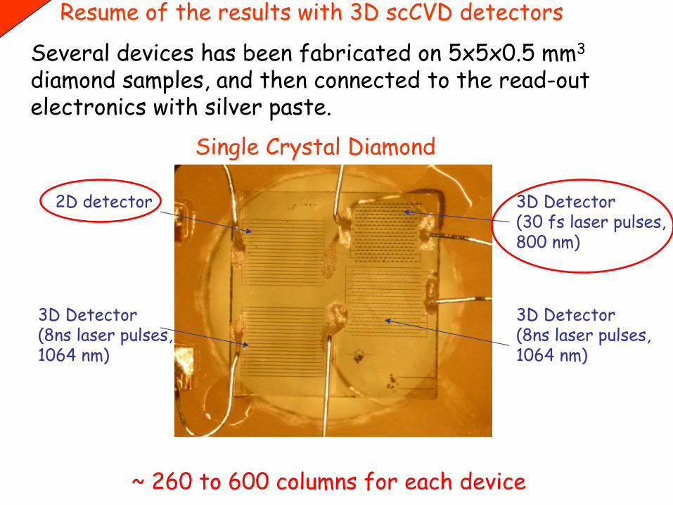
Several devices has been fabricated on 5x5x0.5 mm3 diamond samples, and then connected to the read-out electronics with silver paste.
Single Crystal Diamond
2D detector 3D Detector (30 fs laser pulses, 800 nm)
3D Detector (8ns laser pulses, 1064 nm)
3D Detector (8ns laser pulses, 1064 nm)
~ 260 to 600 columns for each device
Resume of the results with 3D scCVD detectors
Charge collection efficiency of -induced signals in diamond was tested for all the devices fabricated in SCr and PCr diamond.
Resume of the results with 3D scCVD detectors
The 3D columns created with the 30 fs 800 nm pulses exhibit full collection, as well as the reference planar contacts, but saturation takes place at 3V instead of 30 V.
95%.
3 V 30 V
Resume of the results with 3D scCVD detectors
Since we have a detector
- Exhibiting a S/N ratio of about 50 (at 1 s formation time)
- Transit time of the carriers <1ns
- Dark currents 50 fA/column
- Vbias = 3 V
Why to move to poly-crystalline diamond?
Resume of the results with 3D scCVD detectors
Perspectives with pcCVD diamond :
- Price and size (ratio sc/pc CVD 3, diameters of pcCVD wafers of order of inches)
- Shortening the carrier path from 500 m to 70-100 m (without detriment of the overall generated charge) could increase significantly the collected charge.
- pcCVD diamond presents a relatively higher resistance to radiation damage if compared with scCVD (both exhibit comparable efficiencies at 1016 cm-2 28 GeV protons fluence)
Perspectives and problems with pcCVD
Problems with pcCVD diamond:
On the contrary, in the 3D configuration, the reduction of the mean free path can be very relevant.
There has to be a maximum inter-electrode distance to obtain acceptable charge collection.
Perspectives and problems with pcCVD
Grain boundaries are surfaces which high concentration of trapping centers, but the columnar structure of the grains in pcCVD diamond reduces their relevance in conventional planar sensors (the most of the charges are not trapped at the grain boundaries)
Question: how close the columns have to be?
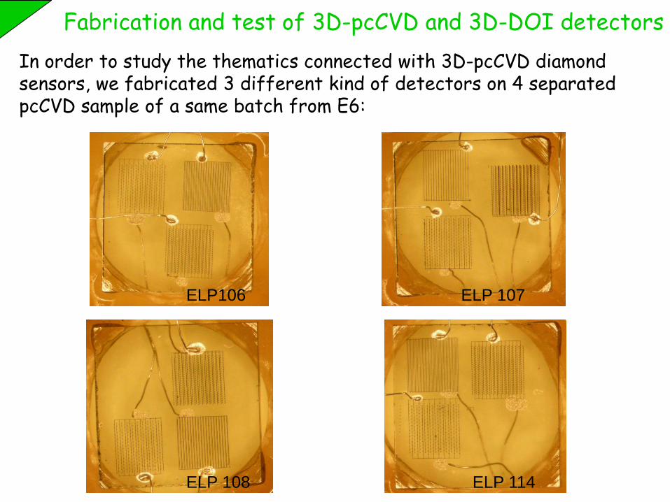
ELP106 ELP 107
ELP 108 ELP 114
Fabrication and test of 3D-pcCVD and 3D-DOI detectors
In order to study the thematics connected with 3D-pcCVD diamond sensors, we fabricated 3 different kind of detectors on 4 separated pcCVD sample of a same batch from E6:
70 m
114 m
100 m
160 m
2D
3D160x100
3D114x70
1.5 mm
1.5 mm
In order to study the thematics connected with 3D-pcCVD diamond sensors, We fabricated 3 different kind of detectors on 4 separated pcCVD sample of a same batch from E6:
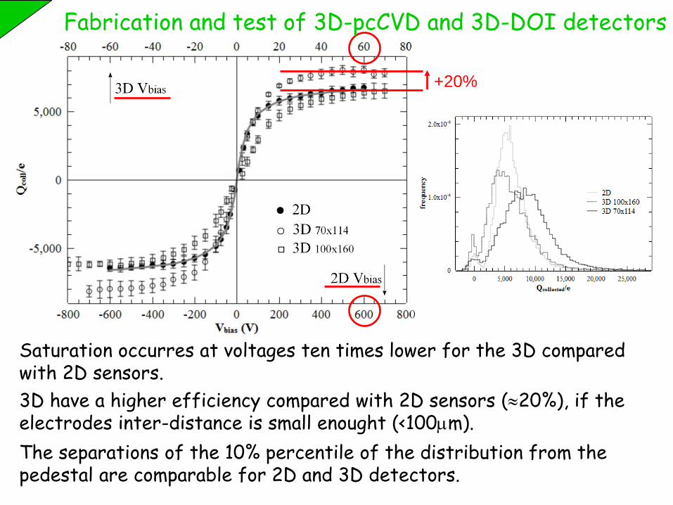
Fabrication and test of 3D-pcCVD and 3D-DOI detectors
3D have a higher efficiency compared with 2D sensors (20%), if the electrodes inter-distance is small enought (<100m).
Saturation occurres at voltages ten times lower for the 3D compared with 2D sensors.
The separations of the 10% percentile of the distribution from the pedestal are comparable for 2D and 3D detectors.
+20%
Fabrication and test of 3D-pcCVD and 3D-DOI detectors
Wgrain Wgrain
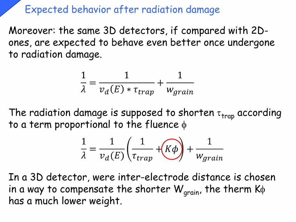
Moreover: the same 3D detectors, if compared with 2D-ones, are expected to behave even better once undergone to radiation damage.
Drift velocity (field dependent)
Mean trapping lenght at the grain boundaries (configuration dependent)
Expected behavior after radiation damage
Mean free path
In a 3D detector, were inter-electrode distance is chosen in a way to compensate the shorter Wgrain, the therm K has a much lower weight.
Moreover: the same 3D detectors, if compared with 2D-ones, are expected to behave even better once undergone to radiation damage.
The radiation damage is supposed to shorten trap according to a term proportional to the fluence
Expected behavior after radiation damage
We have fitted the 2D-sensor S-curve by means of the Hecht formula, in order to calculate trap and Wgrain
2D 3D160x100 3D114x35
trap
Wgrain 160 m
4.3 ns fitted
fitted
Expected behavior after radiation damage
2D 3D160x100 3D114x35
trap
Wgrain
Thus we simulated the charge-collection of 3D-sensors by means of a Monte Carlo algorithm using a three-dimensional finite-element calculation of the electric field, adjusting Wgrain in a way to reproduce the behavior at saturation
4.3 ns 4.3 ns fixed fixed
160 m
4.3 ns fitted
fitted = > Compatible with the columnar size and shape
25 m 25 m
fitted fitted
Expected behavior after radiation damage
Elem. cell
bulk trapping time (configuration-independent) fixed
Effective grain size (different in 3D and 2D) fitted
2D 3D160x100 3D114x35
trap
Wgrain
4.3 ns
160 m
4.3 ns 4.3 ns fixed fixed
25 m 25 m
fitted
fitted fitted fitted
Then we simulated the expected charge collected as a function of k (K depends on the radiation (energy, specie))
We expect, for high fluences, a signal up to 3 times higher for the 3D-sensors, compared to the conventional planar ones.
Expected behavior after radiation damage
3D114x70
3D160x100
2D
We have irradiated our samples at the Jozef Stefan Institute facility of Lubljiana (SLO), at 1MeV-equivalent neutron fluences up to 1.2 x1016cm-2.
Radiation tolerance of 3D-pcCVD detectors, preliminary results
It results a signal from 2 to 3 times higher for the 3D- compared to the 2D-sensors, depending on the fluence experimented.
Radiation tolerance of 3D-pcCVD detectors, preliminary results
We have irradiated our samples at the Jozef Stefan Institute facility of Lubljiana (SLO), at 1MeV-equivalent neutron fluences up to 1.2 x1016cm-2.
Comparison with the RD42 data, referred to 28-GeV protons, requires to take into account a hardness factor of about 6 of the 1-MeV neutrons in comparison to protons.
28 GeV proton fluence
1 MeV neutron fluence
Radiation tolerance of 3D-pcCVD detectors, preliminary results
We have irradiated our samples at the Jozef Stefan Institute facility of Lubljiana (SLO), at 1MeV-equivalent neutron fluences up to 1.2 x1016cm-2.
28 GeV proton fluence
1 MeV neutron fluence
It results that 3D diamond promises to collect at least a double charge than planar one also after proton fluences exceeding 2x1016 cm-2
Radiation tolerance of 3D-pcCVD detectors, preliminary results
We have irradiated our samples at the Jozef Stefan Institute facility of Lubljiana (SLO), at 1MeV-equivalent neutron fluences up to 1.2 x1016cm-2.
Comparison with the simulations gives a quite satisfactory accordance, at least at high fluences, confirming that the better behavior of 3D diamond is due to the lesser weight of the k factor.
28 GeV proton fluence
1 MeV neutron fluence
First data by 3D-DOI detectors
The properties of Diamond-On-Iridium, in which grain boundary formation is hampered by an appropriate texture-growth step, are placed somewhere in the middle between scCVD and pCVD diamond:
• CCE at the level of the best pCVD E6 samples
• Better homogeneity compared to pCVD
• Possibility to produce larger samples than scCVD
We fabricated a 3D 70x114 sensor and a planar sensor also in a DOI sample grown at Augsburg University
In this sample we have inserted an insulated column to also test the behavior of a 1-pixel sensor.
First data by 3D-DOI detectors
We began the measurements very recently, the preliminary results are quite interesting.
First data by 3D-DOI detectors
The sample is about 500 m thick: averall 90Sr- generated charge = 19400 e
Collected charge
2D (at 600 V) = 7600 e (39% CCE)
3D (at 140 V) = 11000 e (58% CCE), relative gain +50%
Results after pumping (>100 Gy -irradiation)
2D signal before pumping 4000 e (21 % CCE)
First data by 3D-DOI detectors
Signal vs. bias voltage characteristics:
Onset bias voltage at
25 V for the 3D sensor
asymmetric (-50 V; +150 V) for the 2D sensor
Suppression of the signal under the threshold partially due to polarization
Q/e
# events
3D bias
2D bias
Conclusions
3D pcCVD diamond sensors exhibit
- Better performance compared to the 2D, in term of saturation bias voltave (1 order of magnitude lower), saturation signal (20% higher), same S/N ratio and dark currents.
- Much higher radiation tolerance. (up to three times higher signals at 1.2x10¹⁶ 1MeV-neutrons/cm2)
- Fabrication of 3D pixel detectors
- Radiation hardness of 3D-DOI detectors?
3D-DOI diamond sensors exhibit
- Even better performances compared to the 2D (signal + 60%)
In the next future:
Acknowledgments
This work is partially supported by GSI, the Helmholtz Center for Heavy-Ion Research in Darmstadt, Germany, in the framework of the Detector Technology and System Platform.