Preprint typeset in JINST style - HYPER VERSION Radiation Tolerance of 65 nm CMOS Transistors M. Krohn a , B. Bentele a , D.C. Christian b* , J.P. Cumalat a , G. Deptuch b , F. Fahim b , J. Hoff b , A. Shenai b , S.R. Wagner a a Department of Physics, University of Colorado, Boulder, Colorado 80309-0390, U.S.A. b Fermi National Accelerator Laboratory, Batavia, IL 60510, U.S.A. E-mail: [email protected]ABSTRACT: We report on the effects of ionizing radiation on 65 nm CMOS transistors held at approximately -20 ◦ C during irradiation. The pattern of damage observed after a total dose of 1 Grad is similar to damage reported in room temperature exposures, but we observe less damage than was observed at room temperature. KEYWORDS: Radiation-hard electronics; Front-end electronics for detector readout. * Corresponding author FERMILAB-PUB-15-014-E ACCEPTED Operated by Fermi Research Alliance, LLC under Contract No. De-AC02-07CH11359 with the United States Department of Energy.
Transcript
Preprint typeset in JINST style - HYPER VERSION
Radiation Tolerance of 65 nm CMOS Transistors
M. Krohna, B. Bentelea, D.C. Christianb∗, J.P. Cumalata, G. Deptuchb, F. Fahimb, J.Hoffb, A. Shenaib, S.R. Wagnera
aDepartment of Physics, University of Colorado,Boulder, Colorado 80309-0390, U.S.A.
bFermi National Accelerator Laboratory,Batavia, IL 60510, U.S.A.E-mail: [email protected]
ABSTRACT: We report on the effects of ionizing radiation on 65 nm CMOS transistors held atapproximately −20 ◦C during irradiation. The pattern of damage observed after a total dose of 1Grad is similar to damage reported in room temperature exposures, but we observe less damagethan was observed at room temperature.
KEYWORDS: Radiation-hard electronics; Front-end electronics for detector readout.
∗Corresponding author
FERMILAB-PUB-15-014-E ACCEPTED
Operated by Fermi Research Alliance, LLC under Contract No. De-AC02-07CH11359 with the United States Department of Energy.
2. Apparatus and Technique 22.1 Test ASIC 22.2 ASIC package, test equipment, and measurement procedures 22.3 Irradiation 3
3. Analysis and Results 7
4. Summary 10
5. Acknowledgments 11
1. Introduction
The need for extremely radiation tolerant electronics is one of the major issues confronting highenergy physics in the era of High Luminosity running at the CERN [1] Large Hadron Collider(HL-LHC). Tests by Bonacini, et al. [2] at CERN, published in 2012, established 65 nm CMOS asthe leading candidate technology for HL-LHC electronics. Using an X-ray beam, Bonacini, et al.exposed 65 nm transistors to a total dose of 200 Mrad. Their results showed, with one exception,relatively small changes in transistor parameters for normal layout standard gate oxide thickness(core) transistors. The exception was a dramatic loss of maximum drain-source current in thenarrowest PMOS transistors. The CERN group concluded that 65 nm CMOS technology could beused for HL-LHC applications with no special design considerations, except that all core devicesshould have width greater than 360 nm.
The RD53 collaboration was formed in 2014 to further explore the feasibility of using 65 nmCMOS technology to design a pixel readout chip for use at the HL-LHC [3]. The group estab-lished a total ionizing dose tolerance goal of 1 Grad. The measurements reported in this paperwere done in the context of RD53. Discussions late in 2013 within RD53 centered on the fact thatthe data presented in reference [2], and also subsequent data collected by the CERN group and bya group from CPPM [4], contain evidence of significant room temperature annealing during thetime between X-ray exposures. Both CMS and ATLAS currently plan to operate their HL-LHCpixel vertex detectors at approximately −20 ◦C. This choice is because the silicon strip trackerswill operate at −20 ◦C in order to limit leakage current in the silicon sensors, which would oth-erwise require much more cooling and therefore more mass in the tracking volume. Concern wasexpressed that because of reduced annealing, 65 nm circuits might experience greater radiationdamage than had been observed in room temperature exposures if the circuits were maintained at−20 ◦C during irradiation.
– 1 –
We report the results of an irradiation of 65 nm transistors performed using the Gamma Irra-diation Facility[5] at Sandia National Laboratories [6]. The devices under test were maintained ata temperature .−20 ◦C during irradiation.
2. Apparatus and Technique
2.1 Test ASIC
A 65 nm CMOS Application Specific Integrated Circuit (ASIC) containing individual transistorsconnected to wire bond pads was designed at Fermilab and fabricated by the Taiwan SemiconductorManufacturing Company (TSMC)[7].1 The test ASIC was part of a multi-project wafer submittedto TSMC through the Metal Oxide Semiconductor Implementation Service (MOSIS)[8]. The chipwas divided into two parts, one part intended primarily for lifetime studies of devices operated atliquid argon temperature, and one part intended for radiation tolerance testing. Transistors intendedfor radiation tolerance testing were laid out in groups of similar transistors (for instance, NMOStransistors with channel length L = 60 nm and width W from 120 nm to 1000 nm). Within agroup, all transistors share a diode-protected gate pad, and an (unprotected) source/drain pad. Theother drain/source of every transistor is connected to its own (unprotected) wire bonding pad. Wetested PMOS and NMOS core (1.2 V) transistors, and NMOS I/O (2.5 V) transistors (with doublethickness gate oxide).
2.2 ASIC package, test equipment, and measurement procedures
The test ASICs were wire bonded into (64-pin) pin grid array (PGA) chip carriers so that theycould be irradiated on simple printed circuit boards (PCBs) containing only sockets for the ASICsand connectors for bias voltages. Transistor characteristics were measured by mounting one chipcarrier at a time on a test board containing switches that allowed individual transistors to be mea-sured independently. The number of pads on the test ASICs was too large to allow all pads to bewire bonded in one package, given the chosen chip carrier, so three different packages with differ-ent wire bonding patterns were made. One package had bonds only to devices intended for coldtests. NMOS transistors were wire bonded in the second package, and PMOS transistors were wirebonded in the third package. The devices intended for cold tests are all large transistors unlikely tobe used in a pixel readout ASIC. They have been excluded from this analysis.
A different PCB was used to test each ASIC package. A simplified schematic of the PCBused to test NMOS transistors is shown in Figure 1. The PCB used to test PMOS transistors wasvery similar. Two Keithley[10] 237 Source Measurement Units (SMUs)[11] were used, one tobias transistor gates, and one to measure drain-souce current. A Labview[12] program runningon a laptop computer was used to sequence and control the measurements. The two SMUs werecontrolled via General Purpose Interface Bus (GPIB)[13]. Logic on the test PCB was controlled viaUSB using a National Instruments[14] USB-6501 I/O board[15], connected to the test PCB by aribbon cable. Bias voltage for the protection diodes was generated by a voltage regulator on the testPCB from the 5 V provided by the laptop USB port. The Labview program controlled solid stateswitches on the test PCB that connected one of the SMUs to a single gate pad at a time; unused
1Our test chip was fabricated at TSMC fab 14; the devices tested earlier at CERN were fabricated at TSMC fab 12[9].
– 2 –
32 pin header 3M2534
5V GND Transistor select (binary number)
74AC111380 Decoder(s)
GND
1
GND
2
…
… TS3A24159
NC72Z04MSX GND SMU #2
Gates
10 posiFon rotary switch
TE ConnecFvity 2-‐435097-‐1
… SMU #1 C
DUT holder: 64 pin socket SSM CPG06402
Drains
Sources GND
Figure 1. Simplified schematic of the PCB used to measure NMOS transistor characteristics.
gates were grounded. The program controlled LEDs on the test PCB to indicate how mechanical(rotary) switches on the test PCB should be set to connect the other SMU to a single transistor drain(unused drains were left floating). All three voltage sources were referenced to a common groundplane on the test PCB, and the source pads for all transistors in a package were connected directlyto this ground. The fact that we did not separate the return current path for the two SMUs, togetherwith possible parasitic circuits involving the protection diodes and the solid state switches in theOFF state, made it impossible for us to accurately measure the leakage current of transistors in theASIC packages.
2.3 Irradiation
The Sandia National Laboratories Gamma Irradiation Facility (GIF) uses 60Co sources to providecontrolled doses of ionizing radiation. 60Co decays by beta decay to an excited state of 60Ni. 60Nirelaxes to the ground state by emitting two gamma rays of energy 1.17 and 1.33 MeV [16]. At theSandia GIF, 60Co is held in stainless steel “source pins” that are 3/8 inch diameter and 18 incheslong. A number of source pins are mounted in an array and to first order, none of the beta electronsescapes the steel source pins. When not in use, the sources are kept at the bottom of an 18 footdeep pool of deionized water which provides shielding. The facility has three shielded irradiationcells in a single high bay area above the shielding pool. Each irradiation cell has an opening in thefloor that allows a source array to be raised out of the water into the cell by an elevator. The cell
– 3 –
that was used in these irradiations contained an array of 40 source pins arranged in a straight line.The array contained approximately 225 kCi of 60Co. Our test ASICs were held inside stainlesssteel thermos bottles (see Figure 2) positioned approximately 2 inches from the face of the sourcearray.2 Cooling was provided by vortex tube coolers [17] mounted in holes drilled through theplastic thermos bottle lids.
The dose rate was 1425 rad/second as measured by an ion chamber placed inside one of thethermos bottles.3 The uniformity of the radiation field was checked by irradiating thermolumines-cent dosimeters (TLDs) taped to each of the chip carriers on the irradiation PCBs. The TLDs wereread at the Radiation Metrology Laboratory at Sandia National Laboratories. The nonuniformitywas measured to be less than 6% RMS by comparing the truncated mean (middle two of four) ofthe four TLDs at each chip carrier position to the average of truncated means, for measurementstaken at the start and end of the irradiation. This variation, which we did not correct for becauseit showed no obvious pattern at the different chip carrier positions, dominates the error on the ionchamber measurement. The TLD measurements also provided a check of the dose rate measuredwith the ion chamber.
Figure 2. Pictures are shown of a thermos bottle assembly, including an irradiation board with four chipcarriers, before insertion of the irradiation board into the thermos bottle. In the left photo, the red arrowpoints to the vortex tube[17] on top of the thermos bottle lid. In the right photo, the red arrow points to anantistatic bag which wraps the irradiation board and (LEMO) low-voltage cable before irradiation. Thesebags separate the boards and voltage cables from the not-very-dry thermos bottle environment, and provideprotection from the metal thermos bottle wall (the test structures are as close to the inner thermos bottle wallas is safe, but not touching). During irradiation, copper pipe was used to deliver air to the vortex tubes.
During irradiation, gamma rays interacted in the walls of the thermos bottles and directly
2The standard practice for 60Co irradiation calls for the electrical devices being tested to be shielded with 1.5mm oflead followed by 0.7 - 1.0 mm of aluminum[20] “in order to minimize dose enhancement effects caused by low-energyscattered radiation.” Our setup did not include a lead-aluminum shielding structure.
3All dosimetry was provided by Sandia National Laboratories.
– 4 –
heated the inside of the thermos bottles. In order to maintain the temperature of the test devices atless than −20 ◦C during long irradiations, especially during daytime when the outside temperaturewas ∼ 35 ◦C, it was necessary to precool the compressed air input to the vortex tubes and to insu-late the copper tubes carrying air to the vortex tubes. Figure 3 shows the temperature of the twothermos bottles during long irradiations. Temperatures were measured using a K-type thermocou-ple in each thermos bottle, read out and recorded with a Fluke 52 II digital thermometer[18]. Thecalibration error for K-type thermocouples used near−20 ◦C is±2.2 ◦C[19]. The precooling of thecompressed air was improved after the first two long irradiations, during which the temperature inone of the two thermos bottles reached −15 ◦C.
Figure 3. The temperature measured inside the two thermos bottles (#1 in blue and #2 in red) during longirradiations. No irradiation was performed during the day on (Saturday) June 8, or on June 9. The two spikeswhere the temperature reached about 8◦C in both thermos bottles for 30 minutes late on June 12 occurredbecause the compressed air unexpectedly shut off.
During irradiation the chip carriers were mounted in sockets on irradiation PCBs. Each irradi-ation PCB held four chip carriers (see Figure 2), two for PMOS packages, and one each for NMOSand cold transistor packages. Transistor bias voltages were provided by Keithley 237 SMUs (lo-cated outside the shielded irradiation cell) connected to the irradiation PCBs by 20 foot long triaxcables. The PMOS transistors were biased in two different ways. In one package, the drains,sources, and gates were held at 1.2 V and the substrate was grounded; the other package was bi-ased with all the gates and the substrate grounded, while the drains and sources were held at 1.2V. The gates of both the core NMOS and the I/O NMOS were biased at 1.2 V; all other nodeswere grounded. Twelve irradiations were performed over 15 days, as shown in Table 1. After eachirradiation step, a single characteristic curve was recorded for each transistor. All measurementswere made at room temperature. The drain-source voltage was set to 1.2 V and the drain-source
current was measured as the gate-source voltage was swept from 0 to 1.2 V. It took∼10 minutes totest the transistors in each package. The ASIC packages were kept at −20 ◦C in a freezer when notbeing tested or irradiated.
Pre-irradiation measurements of the transistors showed that a small number of transistors werebroken either in fabrication or in the wire bonding process. Approximately half of the transistorsthat were irradiated failed during the 15 days at Sandia. One group of 12 NMOS transistors wasbroken mechanically by mishandling. Most of the other transistors that failed also did so in groups,but without an obvious cause. We replaced the package containing the group of 12 failed NMOStransistors partway through the irradiation. The replacement package received a total dose of 878Mrad. Tables 2 and 3 list all of the transistors included in this study and note which transistorsfailed and when the failures occurred. Broken transistors were easily identified. For many, thedrain-source current was either very small or very large, independent of gate bias. For a smallernumber, the drain-source current varied approximately linearly with gate bias.
The most likely cause of transistor failures is electrostatic discharge (ESD). We took a numberof steps to reduce the probability of ESD, but our procedures had some deficiencies. The chipcarrier packages were transported in an antistatic box and when a package was mounted on, orremoved from a PCB, the work was done on a grounded antistatic mat by a person wearing a wristgrounding strap. The PCB was grounded before a chip carrier was inserted into or removed froma socket, but no ESD precautions were taken when the irradiation PCBs were inserted into thethermos bottles or when bias cables were connected. All transistor gate pads were diode protectedon-chip, but none of the source or drain pads was ESD protected. Moreover, bias for the on-chipprotection diodes was provided through only one pin of the PGA chip carriers. If this pin failedto make contact before other pins while a package was being inserted into a socket, the protectiondiodes may not have been biased when they were needed most.
After the irradiations, the devices were kept at−20 ◦C in a freezer that could be powered eitherby 120 V or by 12 V and transported to Fermilab. Once at Fermilab the transistors were removed
– 6 –
Table 2. NMOS transistors: Each entry in one of the last three columns corresponds to a transistor andindicates the dose accumulated before the transistor was broken. Transistors that were not broken have noentry. Zero indicates a transistor that was broken before irradiation. Transistors in the upper part of the tablehave standard thickness gate oxide; those in the lower part have gate oxide that is twice normal thickness.All transistors are standard layout unless otherwise indicated; ELT indicates enclosed layout. Transistorsthat share a gate pad are grouped together. IC2 received the full dose of 1.1 Grad; IC3 was replaced by IC1after a dose of 215 Mrad, so IC1 received 878 Mrad. IC1 and IC3 were irradiated in thermos #1; IC2 wasirradiated in thermos #2.
400/280 3 754500/280 3 754800/280 3 7541000/280 3 7545000/500 3 7545000/5000 3 7542220/280 ELT 3 7543380/1200 Zero Vt ELT 3 754400/280 Triple well 3 426 754800/280 Triple well 3 754
from the freezer and kept at room temperature for one week. Multiple measurements were takenduring this time. Then the transistors were held in an oven at 100 ◦C for another week and a finalset of measurements was made. This annealing schedule can be seen in Table 4. The transistorswere not biased during transport or annealing.
3. Analysis and Results
Two quantities were extracted from each transistor characteristic: the maximum drain-source cur-rent and the (saturation) threshold voltage Vth. The quadratic extrapolation method was used to
– 7 –
Table 3. PMOS transistors: Each entry in one of the last four columns corresponds to a transistor andindicates the dose accumulated before the transistor was broken. Transistors that were not broken have noentry. IC4 and IC6 were biased with Vs = Vd = Vg. IC5 and IC7 were biased with Vs = Vd = 1.2 V andVg =GND. All four packages received the full dose of 1.1 Grad. IC4 and IC5 were irradiated in thermos #2;IC6 and IC7 were irradiated in thermos #1.
Table 4. The annealing times and temperatures of the transistors.Annealing Schedule
June 16-24 −20◦C 8 DaysJune 24 - July 1 Room Temperature 7 DaysJuly 1-8 100 ◦C 7 Days
0 0.2 0.4 0.6 0.8 1 1.2
)1/
2 (
AId
s
0
0.002
0.004
0.006
0.008
0.01
0.012 Vth = 0.366V
Ids
Vgs(V)
)V1/
2A
(Vgs
)(∆
)/Id
s(
∆
0
0.002
0.004
0.006
0.008
0.01
0.012
0.014
0.016
(Vgs)∆)/Ids(∆
/dVgsIdsd
Figure 4. This figure illustrates the quadratic extrapolation method used to determine the (saturation) thresh-old voltage (Vth) of an NMOS transistor. The data shown is from the pre-irradiation measurement of the240/60 transistor in IC3. For PMOS transistors, |Ids| is used since Ids is negative.
determine the threshold voltage[21]. As shown in Figure 4, Vth is defined to be the voltage at which
a line tangent to the curve√|Ids| vs Vgs at the point of maximum d
√|Ids|
dVgsintercepts the Ids = 0
axis. We determined the slope of the curve by fitting it with a fifth order polynomial and dif-
– 8 –
ferentiating the fit function. In Figure 4, the red squares were computed using finite differences(√Ids(N+1)−
√Ids(N)
Vgs(N+1)−Vgs(N)
); the black line is the result of differentiating the fit to the curve
Figure 5. Transistor characteristic curves for total dose up to 1.1 Grad of (upper left) a 120/60 core PMOS,(upper right) a 360/60 core PMOS, and for total dose up to 878 Mrad of (lower left) a 240/60 core NMOS,and (lower right) a 1000/280 2.5 V NMOS.
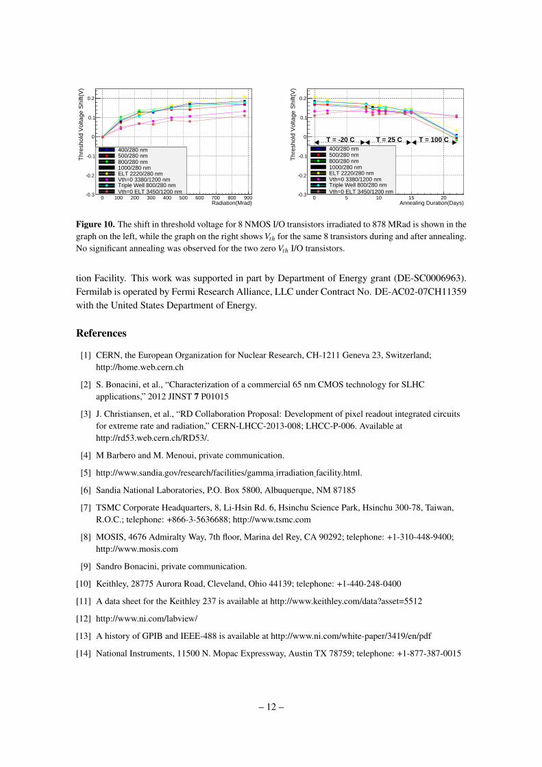
Figure 5 illustrates the radiation effects observed in our data. The most prominent effect is adecrease of the maximum drain-source current of core PMOS transistors. The fractional decreaseis largest for the smallest PMOS transistors; the maximum drain-source current of the smallestPMOS decreased by more than a factor of two. The maximum drain-source current of core NMOStransistors also decreased, but only by ∼ 5−10%. No significant threshold shift was observed forany of the core transistors, but the threshold voltage of NMOS I/O transistors increased by 100 -200 mV. No error bars are included in the figures because the uncertainty in the SMU measurementsis smaller than the symbols used to plot the measurements.
No significant difference was observed between the radiation-induced changes of PMOS tran-sistors biased during the irradiation with the gate in the ON state and PMOS transistors biased withthe gate in the OFF state. This is illustrated in Figure 6.
Figure 7 demonstrates the annealing effects observed in our data. Both the PMOS core tran-sistors and the NMOS I/O transistors recovered significantly during the annealing period.
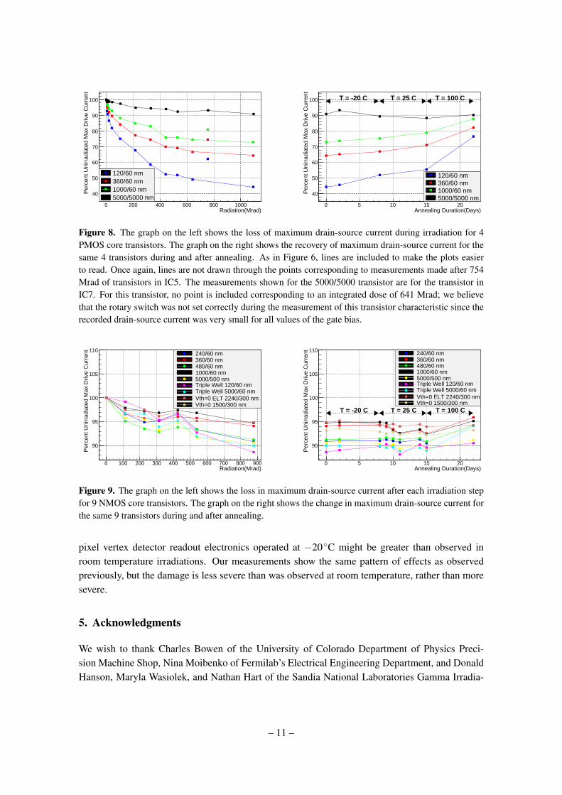
Figures 8 and 9 show the evolution of the maximum drain-source current for a representativeselection of PMOS and NMOS core transistors during irradiation and annealing. We did not ob-serve any significant differences in the effect of radiation on the various different types of NMOS
– 9 –
Radiation(Mrad)0 200 400 600 800 1000
Per
cent
Uni
rrad
iate
d M
ax D
rive
Cur
rent
50
60
70
80
90
100 Gate Bias = 1.2 V
Gate Bias = 1.2 V
Gate Bias = GND
Radiation(Mrad)0 200 400 600 800 1000
Per
cent
Uni
rrad
iate
d M
ax D
rive
Cur
rent
50
60
70
80
90
100 Gate Bias = 1.2 V
Gate Bias = 1.2 V
Gate Bias = GND
Figure 6. The change in maximum drain-source current for similar PMOS core transistors irradiated withdifferent gate bias voltages. The graph on the left is for 120/60 transistors and the graph on the right is for360/60 transistors. The lines connecting points do not represent a fit, and are included only to make theplots easier to read. The transistor characteristics measured for transistors in package IC5 after 754 Mradwas accumulated were all offset by current not likely to have passed through the transistors (this can be seenin Figure 5). Lines are not drawn through these points. The most likely source of these offsets is leakagecurrent due to moisture caused by condensation on the cold IC package.
Vgs(V)-1.2 -1 -0.8 -0.6 -0.4 -0.2 0
(A)
Ids
0
0.01
0.02
0.03
0.04
0.05
-310×0 Mrad1093 Mrad2 Days -20 C7 Days Room Temp7 Days 100 C
Vgs(V)0 0.2 0.4 0.6 0.8 1 1.2
Ids(
A)
0
0.01
0.02
0.03
0.04
0.05
0.06
-310×0 Mrad878 Mrad2 Days -20 C8 Days -20 C1 Day Room Temp2 Days Room Temp3 Days Room Temp6 Days Room Temp7 Days Room Temp7 Days 100 C
Figure 7. Transistor chararcteristic curves during the annealing period for (left) a 120/60 core PMOS and(right) a 1000/280 2.5 V NMOS.
transistors tested (normal layout, enclosed layout, triple well, and zero Vth). Figure 10 showsthe threshold shift of a representative selection of NMOS I/O transistors during irradiation andannealing.
4. Summary
Previous measurements have established 65 nm CMOS as the leading candidate technology for HL-LHC electronics. After an exposure of 200 Mrad, Bonacini, et al. reported [2], with one exception,only minor changes in transistor parameters. The exception was a significant loss of maximumdrain-source current by narrow PMOS core transistors. They reported a 50% reduction in maximumdrive current for a 120/60 PMOS core transistor and a 35% loss for a 360/60 PMOS core transistor.This irradiation of “cold” 65 nm CMOS transistors was motivated by a concern that damage to
– 10 –
Radiation(Mrad)0 200 400 600 800 1000
Per
cent
Uni
rrad
iate
d M
ax D
rive
Cur
rent
40
50
60
70
80
90
100
120/60 nm360/60 nm1000/60 nm5000/5000 nm
Annealing Duration(Days)0 5 10 15 20
Per
cent
Uni
rrad
iate
d M
ax D
rive
Cur
rent
40
50
60
70
80
90
100
120/60 nm360/60 nm1000/60 nm5000/5000 nm
T = -20 C T = 25 C T = 100 C
Figure 8. The graph on the left shows the loss of maximum drain-source current during irradiation for 4PMOS core transistors. The graph on the right shows the recovery of maximum drain-source current for thesame 4 transistors during and after annealing. As in Figure 6, lines are included to make the plots easierto read. Once again, lines are not drawn through the points corresponding to measurements made after 754Mrad of transistors in IC5. The measurements shown for the 5000/5000 transistor are for the transistor inIC7. For this transistor, no point is included corresponding to an integrated dose of 641 Mrad; we believethat the rotary switch was not set correctly during the measurement of this transistor characteristic since therecorded drain-source current was very small for all values of the gate bias.
110240/60 nm360/60 nm480/60 nm1000/60 nm5000/500 nmTriple Well 120/60 nmTriple Well 5000/60 nmVth=0 ELT 2240/300 nmVth=0 1500/300 nm
Annealing Duration(Days)0 5 10 15 20
Per
cent
Uni
rrad
iate
d M
ax D
rive
Cur
rent
90
95
100
105
110 240/60 nm360/60 nm480/60 nm1000/60 nm5000/500 nmTriple Well 120/60 nmTriple Well 5000/60 nmVth=0 ELT 2240/300 nmVth=0 1500/300 nm
T = -20 C T = 25 C T = 100 C
Figure 9. The graph on the left shows the loss in maximum drain-source current after each irradiation stepfor 9 NMOS core transistors. The graph on the right shows the change in maximum drain-source current forthe same 9 transistors during and after annealing.
pixel vertex detector readout electronics operated at −20 ◦C might be greater than observed inroom temperature irradiations. Our measurements show the same pattern of effects as observedpreviously, but the damage is less severe than was observed at room temperature, rather than moresevere.
5. Acknowledgments
We wish to thank Charles Bowen of the University of Colorado Department of Physics Preci-sion Machine Shop, Nina Moibenko of Fermilab’s Electrical Engineering Department, and DonaldHanson, Maryla Wasiolek, and Nathan Hart of the Sandia National Laboratories Gamma Irradia-
Figure 10. The shift in threshold voltage for 8 NMOS I/O transistors irradiated to 878 MRad is shown in thegraph on the left, while the graph on the right shows Vth for the same 8 transistors during and after annealing.No significant annealing was observed for the two zero Vth I/O transistors.
tion Facility. This work was supported in part by Department of Energy grant (DE-SC0006963).Fermilab is operated by Fermi Research Alliance, LLC under Contract No. DE-AC02-07CH11359with the United States Department of Energy.
References
[1] CERN, the European Organization for Nuclear Research, CH-1211 Geneva 23, Switzerland;http://home.web.cern.ch
[2] S. Bonacini, et al., “Characterization of a commercial 65 nm CMOS technology for SLHCapplications,” 2012 JINST 7 P01015
[3] J. Christiansen, et al., “RD Collaboration Proposal: Development of pixel readout integrated circuitsfor extreme rate and radiation,” CERN-LHCC-2013-008; LHCC-P-006. Available athttp://rd53.web.cern.ch/RD53/.
[4] M Barbero and M. Menoui, private communication.
[11] A data sheet for the Keithley 237 is available at http://www.keithley.com/data?asset=5512
[12] http://www.ni.com/labview/
[13] A history of GPIB and IEEE-488 is available at http://www.ni.com/white-paper/3419/en/pdf
[14] National Instruments, 11500 N. Mopac Expressway, Austin TX 78759; telephone: +1-877-387-0015
– 12 –
[15] A data sheet for the NI USB-6501 is available at http://www.ni.com/datasheet/pdf/en/ds-135
[16] K.A. Olive, et al. (Particle Data Group), Chin. Phys. C, 38, 090001 (2014), page 466
[17] Vortec 106-4-H vortex tubes were purchased from Vortec (www.vortec.com), part of the ITW AirManagement business unit of Illinois Tool Works.
[18] Fluke Corporation, 6920 Seaway Boulevard, Everett, WA 98206; telephone: +1-425 347-6100Specifications for the Fluke 52 digital thermometer are available athttp://en-us.fluke.com/products/thermometers/fluke-52-ii-thermometer.html#techspecs
[19] “Manual on the Use of Thermocouples in Temperature Measurement: 4th Edition,” ASTMInternational, West Conshohocken, PA, 2014 (1993).
[20] ASTM Standard F1892-12, 2012, “Standard Guide for Ionizing Radiation (Total Dose) EffectsTesting of Semiconductor Devices," ASTM International, West Conshohocken, PA,2014,DOI:10.1520/F1892-12, http://www.astm.org.
[21] Dieter K. Schroder, Semiconductor Material and Device Characterization, John Wiley and Sons, Inc.,New York 1998.