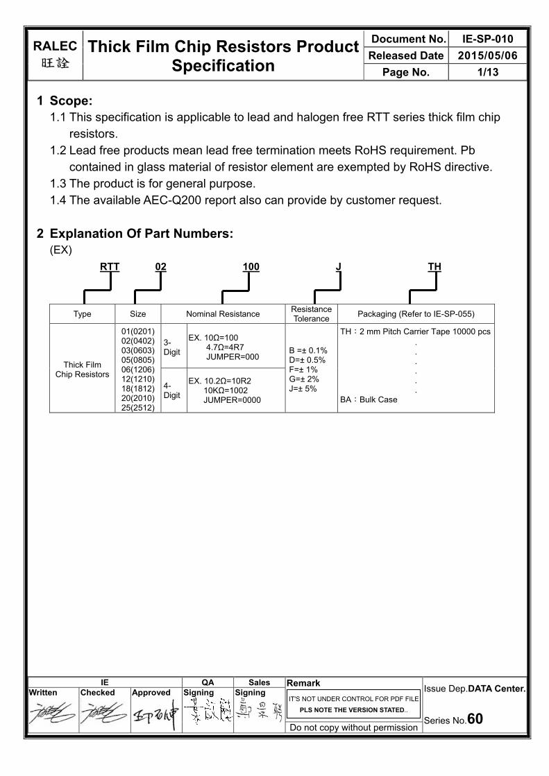
RALEC 旺詮 Thick Film Chip Resistors Product Specification Document No. IE-SP-010 Released Date 2015/05/06 Page No. 1/13 IE QA Sales Remark Issue Dep.DATA Center. Series No.60 Written Checked Approved Signing Signing Do not copy without permission IT'S NOT UNDER CONTROL FOR PDF FILE PLS NOTE THE VERSION STATED.. 1 Scope: 1.1 This specification is applicable to lead and halogen free RTT series thick film chip resistors. 1.2 Lead free products mean lead free termination meets RoHS requirement. Pb contained in glass material of resistor element are exempted by RoHS directive. 1.3 The product is for general purpose. 1.4 The available AEC-Q200 report also can provide by customer request. 2 Explanation Of Part Numbers: (EX) RTT 02 100 J TH Type Size Nominal Resistance Resistance Tolerance Packaging (Refer to IE-SP-055) Thick Film Chip Resistors 01(0201) 02(0402) 03(0603) 05(0805) 06(1206) 12(1210) 18(1812) 20(2010) 25(2512) 3- Digit EX. 10Ω=100 4.7Ω=4R7 JUMPER=000 B =± 0.1% D=± 0.5% F=± 1% G=± 2% J=± 5% TH:2 mm Pitch Carrier Tape 10000 pcs . . . . . . BA:Bulk Case 4- Digit EX. 10.2Ω=10R2 10KΩ=1002 JUMPER=0000
Transcript
RALEC 旺詮
Thick Film Chip Resistors Product Specification
Document No. IE-SP-010 Released Date 2015/05/06
Page No. 1/13
IE QA Sales Remark Issue Dep.DATA Center.
Series No.60
Written
Checked
Approved
Signing Signing
Do not copy without permission
IT'S NOT UNDER CONTROL FOR PDF FILE
PLS NOTE THE VERSION STATED..
1 Scope: 1.1 This specification is applicable to lead and halogen free RTT series thick film chip
resistors. 1.2 Lead free products mean lead free termination meets RoHS requirement. Pb
contained in glass material of resistor element are exempted by RoHS directive. 1.3 The product is for general purpose. 1.4 The available AEC-Q200 report also can provide by customer request.
2 Explanation Of Part Numbers:
(EX) RTT 02 100 J TH
Type Size Nominal Resistance ResistanceTolerance Packaging (Refer to IE-SP-055)
IT'S NOT UNDER CONTROL FOR PDF FILE PLS NOTE THE VERSION STATED..
3.3 Power Derating Curve: Type RTT01 (0201) Other
Operating Temperature
Range -55 ~ +125 -55 ~ +155
Explain For resistors operated in ambient temperatures above 70, power rating shall be derated in accordance with figure below.
For resistors operated in ambient temperatures above 70, power rating shall be derated in accordance with figure below.
Figure
100
80
60
40
20
020 40 60 80 100 120
125
Ambient temperature ( )
70
140 160-55
Rat
ed P
ower
(%)
100
80
60
40
20
020 40 60 80 100 120
155
70
140 160-55
Rat
ed P
ower
(%)
Ambient temperature ( )
3.4 Voltage Rating or Current Rating
3.4.1Resistance Range:≧1Ω Rated Voltage: The resistor shall have a DC continuous working voltage or a rms. AC continuous working voltage at commercial-line frequency and wave form corresponding to the power rating, as determined from the following
E = R×P E= Rated voltage (v) P= Power rating (w) R= Nominal resistance(Ω)
3.4.2Range:<1Ω
Rated Current: The resistor shall have a DC continuous working current or a rms. AC continuous working current at commercial-line frequency and wave form corresponding to the power rating, as determined from the following:
I= Rated current (A) P= Power rating (w) R= Nominal resistance(Ω)
RALEC 旺詮
Thick Film Chip Resistors Product Specification
Document No. IE-SP-010 Released Date 2015/05/06
Page No. 5/13
Remark
Issue Dep.DATA Center.
Series No.60 Do not copy without permission
IT'S NOT UNDER CONTROL FOR PDF FILE PLS NOTE THE VERSION STATED..
IT'S NOT UNDER CONTROL FOR PDF FILE PLS NOTE THE VERSION STATED..
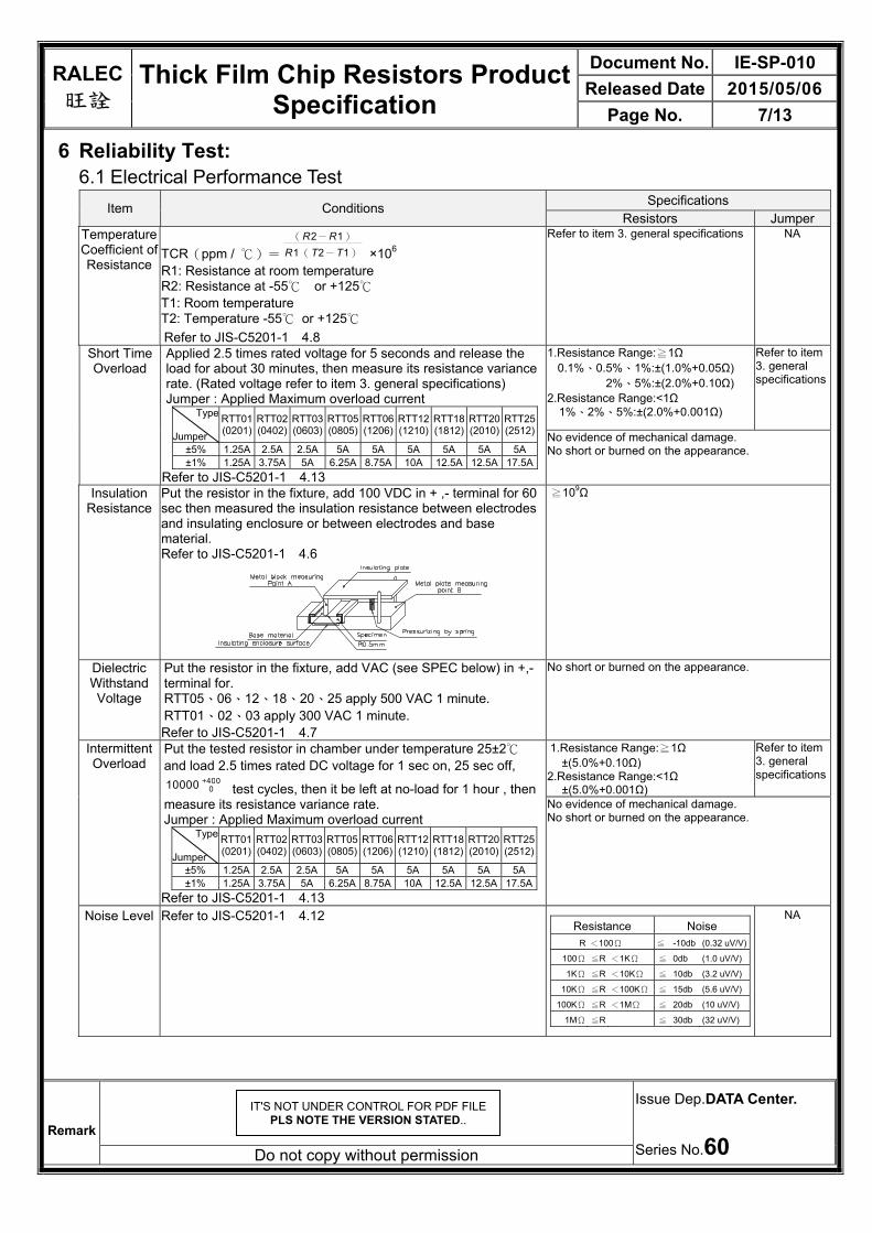
6 Reliability Test: 6.1 Electrical Performance Test
Item Conditions Specifications Resistors Jumper
Temperature Coefficient of Resistance
TCR(ppm / )=
(R2-R1)
R1(T2-T1) ×106 R1: Resistance at room temperature R2: Resistance at -55 or +125 T1: Room temperature T2: Temperature -55 or +125 Refer to JIS-C5201-1 4.8
Refer to item 3. general specifications NA
Short Time Overload
Applied 2.5 times rated voltage for 5 seconds and release the load for about 30 minutes, then measure its resistance variance rate. (Rated voltage refer to item 3. general specifications) Jumper : Applied Maximum overload current
No evidence of mechanical damage. No short or burned on the appearance.
Insulation Resistance
Put the resistor in the fixture, add 100 VDC in + ,- terminal for 60 sec then measured the insulation resistance between electrodes and insulating enclosure or between electrodes and base material. Refer to JIS-C5201-1 4.6
≧109Ω
Dielectric Withstand Voltage
Put the resistor in the fixture, add VAC (see SPEC below) in +,- terminal for. RTT05、06、12、18、20、25 apply 500 VAC 1 minute. RTT01、02、03 apply 300 VAC 1 minute. Refer to JIS-C5201-1 4.7
No short or burned on the appearance.
Intermittent Overload
Put the tested resistor in chamber under temperature 25±2 and load 2.5 times rated DC voltage for 1 sec on, 25 sec off, 10000 +400
0 test cycles, then it be left at no-load for 1 hour , then measure its resistance variance rate. Jumper : Applied Maximum overload current
No evidence of mechanical damage. No short or burned on the appearance.
Noise Level Refer to JIS-C5201-1 4.12 Resistance Noise
R <100Ω ≦ -10db (0.32 uV/V)
100Ω ≦R <1KΩ ≦ 0db (1.0 uV/V)
1KΩ ≦R <10KΩ ≦ 10db (3.2 uV/V)
10KΩ ≦R <100KΩ ≦ 15db (5.6 uV/V)
100KΩ ≦R <1MΩ ≦ 20db (10 uV/V)
1MΩ ≦R ≦ 30db (32 uV/V)
NA
RALEC 旺詮
Thick Film Chip Resistors Product Specification
Document No. IE-SP-010 Released Date 2015/05/06
Page No. 8/13
Remark
Issue Dep.DATA Center.
Series No.60 Do not copy without permission
IT'S NOT UNDER CONTROL FOR PDF FILE PLS NOTE THE VERSION STATED..
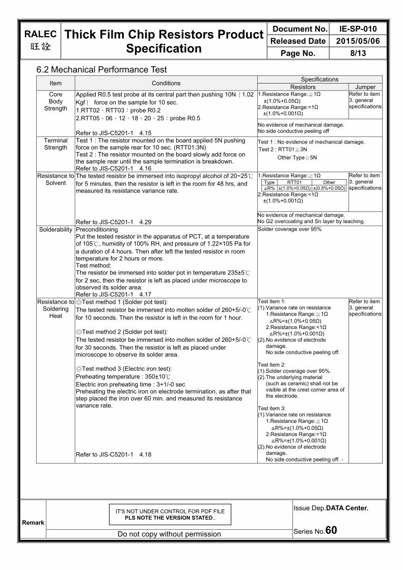
6.2 Mechanical Performance Test Item Conditions Specifications
Resistors Jumper Core Body
Strength
Applied R0.5 test probe at its central part then pushing 10N{1.02 Kgf} force on the sample for 10 sec. 1.RTT02、RTT03:probe R0.2 2.RTT05、06、12、18、20、25:probe R0.5
Refer to JIS-C5201-1 4.15
1.Resistance Range:≧1Ω ±(1.0%+0.05Ω)
2.Resistance Range:<1Ω ±(1.0%+0.001Ω)
Refer to item 3. general specifications
No evidence of mechanical damage. No side conductive peeling off
Terminal Strength
Test 1 : The resistor mounted on the board applied 5N pushing force on the sample rear for 10 sec. (RTT01:3N) Test 2 : The resistor mounted on the board slowly add force on the sample rear until the sample termination is breakdown. Refer to JIS-C5201-1 4.16
Test 1 : No evidence of mechanical damage. Test 2 : RTT01≧3N
Other Type≧5N
Resistance to Solvent
The tested resistor be immersed into isopropyl alcohol of 20~25 for 5 minutes, then the resistor is left in the room for 48 hrs, and measured its resistance variance rate. Refer to JIS-C5201-1 4.29
1.Resistance Range:≧1Ω Type RTT01 Other R% ±(1.0%+0.05Ω) ±(0.5%+0.05Ω)
2.Resistance Range:<1Ω ±(1.0%+0.001Ω)
Refer to item 3. general specifications
No evidence of mechanical damage. No G2 overcoating and Sn layer by leaching.
Solderability Preconditioning Put the tested resistor in the apparatus of PCT, at a temperature of 105, humidity of 100% RH, and pressure of 1.22×10⁵ Pa for a duration of 4 hours. Then after left the tested resistor in room temperature for 2 hours or more. Test method: The resistor be immersed into solder pot in temperature 235±5 for 2 sec, then the resistor is left as placed under microscope to observed its solder area. Refer to JIS-C5201-1 4.17
Solder coverage over 95%
Resistance to Soldering
Heat
Test method 1 (Solder pot test): The tested resistor be immersed into molten solder of 260+5/-0 for 10 seconds. Then the resistor is left in the room for 1 hour. Test method 2 (Solder pot test): The tested resistor be immersed into molten solder of 260+5/-0 for 30 seconds. Then the resistor is left as placed under microscope to observe its solder area. Test method 3 (Electric iron test): Preheating temperature : 350±10 Electric iron preheating time : 3+1/-0 sec Preheating the electric iron on electrode termination, as after that step placed the iron over 60 min. and measured its resistance variance rate. Refer to JIS-C5201-1 4.18
(2).No evidence of electrode damage. No side conductive peeling off.。
Refer to item 3. general specifications
RALEC 旺詮
Thick Film Chip Resistors Product Specification
Document No. IE-SP-010 Released Date 2015/05/06
Page No. 9/13
Remark
Issue Dep.DATA Center.
Series No.60 Do not copy without permission
IT'S NOT UNDER CONTROL FOR PDF FILE PLS NOTE THE VERSION STATED..
Item Conditions Specifications Resistors Jumper
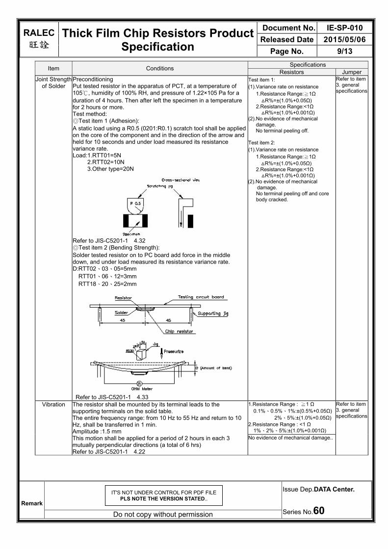
Joint Strength of Solder
Preconditioning Put tested resistor in the apparatus of PCT, at a temperature of 105, humidity of 100% RH, and pressure of 1.22×10⁵ Pa for a duration of 4 hours. Then after left the specimen in a temperature for 2 hours or more. Test method: Test item 1 (Adhesion): A static load using a R0.5 (0201:R0.1) scratch tool shall be applied on the core of the component and in the direction of the arrow and held for 10 seconds and under load measured its resistance variance rate. Load:1.RTT01=5N
2.RTT02=10N 3.Other type=20N
Refer to JIS-C5201-1 4.32 Test item 2 (Bending Strength): Solder tested resistor on to PC board add force in the middle down, and under load measured its resistance variance rate. D:RTT02、03、05=5mm
(2).No evidence of mechanical damage. No terminal peeling off and core body cracked.
Refer to item 3. general specifications
Vibration The resistor shall be mounted by its terminal leads to the supporting terminals on the solid table. The entire frequency range: from 10 Hz to 55 Hz and return to 10 Hz, shall be transferred in 1 min. Amplitude :1.5 mm This motion shall be applied for a period of 2 hours in each 3 mutually perpendicular directions (a total of 6 hrs) Refer to JIS-C5201-1 4.22
1.Resistance Range : ≧1 Ω 0.1%、0.5%、1%:±(0.5%+0.05Ω) 2%、5%:±(1.0%+0.05Ω)2.Resistance Range : <1 Ω 1%、2%、5%:±(1.0%+0.001Ω)
Refer to item 3. general specifications
No evidence of mechanical damage..
RALEC 旺詮
Thick Film Chip Resistors Product Specification
Document No. IE-SP-010 Released Date 2015/05/06
Page No. 10/13
Remark
Issue Dep.DATA Center.
Series No.60 Do not copy without permission
IT'S NOT UNDER CONTROL FOR PDF FILE PLS NOTE THE VERSION STATED..
6.3 Environmental Test Item Conditions
Specifications Resistors Jumper
Resistance to Dry Heat
Put tested resistor in chamber under temperature 155±5 for 1000 +48/-0 hours. Then leaving the tested resistor in room temperature for 60 minutes, and measure its resistance variance rate.(RTT01 for 125±3) Refer to JIS-C5201-1 4.25
1.Resistance Range:≧1Ω 0.1%、0.5%、1%:±(1.0%+0.05Ω)
2%、5%:±(2.0%+0.10Ω)2.Resistance Range:<1Ω
1%、2%、5%:±(1.0%+0.001Ω)
Refer to item 3. general specifications
No evidence of mechanical damage. No short or burned on the appearance.
Thermal Shock Put the tested resistor in the chamber under the Thermal Shock which shown in the following table shall be repeated 300 times consecutively. Then leaving the tested resistor in the room temperature for 1 hours, and measure its resistance variance rate.
Testing Condition Lowest Temperature -55±5 Highest Temperature 125±5
Temperature-retaining time 15 minutes each Refer to MIL-STD 202 Method 107
1.Resistance Range:≧1Ω 0.1%、0.5%、1%:±(0.5%+0.05Ω)
2%、5%:±(1.0%+0.05Ω)2.Resistance Range:<1Ω
1%、2%、5%:±(1.0%+0.001Ω)
Refer to item 3. general specifications
No evidence of mechanical damage. No short or burned on the appearance.
Loading Life in Moisture
Put the tested resistor in the chamber under temperature 40±2, relative humidity 90~95% and load the rated voltage for 90 minutes on, 30 minutes off, total 1000 hours. Then leaving the tested resistor in room temperature for 60 minutes, and measure its resistance variance rate. Refer to JIS-C5201-1 4.24
1.Resistance Range:≧1Ω Type RTT01 Other
Range
1%: ±(1.0%+0.05Ω) 5%: ±(3.0%+0.1Ω)
0.1%、0.5%、1%:±(0.5%+0.05Ω) 2%、5%: ±(2.0%+0.10Ω)
2.Resistance Range:<1Ω 1%、2%、5%:±(2.0%+0.001Ω)
Refer to item 3. general specifications
No evidence of mechanical damage. No short or burned on the appearance.
Load Life Put the tested resistor in chamber under temperature 70±2 and load the rated voltage for 90 minutes on, 30 minutes off, total 1000 hours. Then leaving the tested resistor in room temperature for 60 minutes, and measure its resistance variance rate. Refer to JIS-C5201-1 4.25
1.Resistance Range:≧1Ω Type RTT01 Other
Range
1%: ±(1.0%+0.05Ω) 5%: ±(3.0%+0.1Ω)
0.1%、0.5%、1%:±(0.5%+0.05Ω) 2%、5%: ±(2.0%+0.10Ω)
2.Resistance Range:<1Ω 1%、2%、5%:±(2.0%+0.001Ω)
Refer to item 3. general specifications
No evidence of mechanical damage. No short or burned on the appearance.
Low Temperature
Operation
Put the tested resistor in the chamber at room temperature 25.Decreasing the temperature to -55 and keep the temperature at -55 for 1 hour. Then load the rated voltage for 45 minutes on, and 15 minutes off. Then leaving the tested resistor in room temperature for 8±1 hours, and measure its resistance variance rate. Refer to MIL-R-55342D 4.7.4
1.Resistance Range:≧1Ω 0.1%、0.5%、1%:±(0.5%+0.05Ω)
2%、5%:±(1.0%+0.05Ω)2.Resistance Range:<1Ω
1%、2%、5%:±(1.0%+0.001Ω)
Refer to item 3. general specifications
No evidence of mechanical damage. No short or burned on the appearance.
Whisker Test Test item (Thermal Shock test): Testing Condition
Minimum storage temperature -55+0/-10 Maximum storage temperature 85+10/-0
Temperature-retaining time 10 min.Number of temperature cycles 1,500
Inspection: Inspect for whisker formation on specimens that underwent the acceleration test specified in subciause 4.2, with a magnifier (stereo microscope) of about 40 or higher magnification. If judgment is hard in this method, use a scanning electron microscope (SEM) of about 1,000 or higher magnification. By JESD Standard NO.22A121 class 2.
Max. 50μm
RALEC 旺詮
Thick Film Chip Resistors Product Specification
Document No. IE-SP-010 Released Date 2015/05/06
Page No. 11/13
Remark
Issue Dep.DATA Center.
Series No.60 Do not copy without permission
IT'S NOT UNDER CONTROL FOR PDF FILE PLS NOTE THE VERSION STATED..
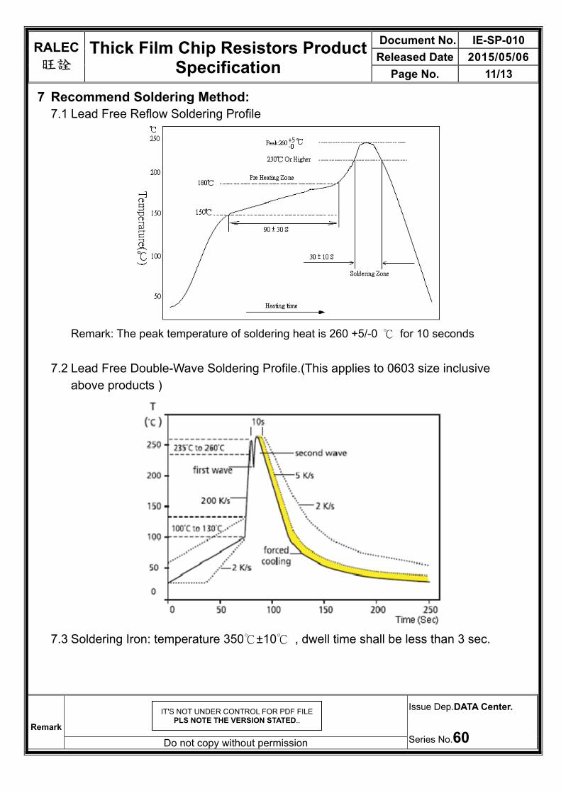
7 Recommend Soldering Method: 7.1 Lead Free Reflow Soldering Profile
Remark: The peak temperature of soldering heat is 260 +5/-0 for 10 seconds
7.2 Lead Free Double-Wave Soldering Profile.(This applies to 0603 size inclusive
above products )
7.3 Soldering Iron: temperature 350±10 , dwell time shall be less than 3 sec.
RALEC 旺詮
Thick Film Chip Resistors Product Specification
Document No. IE-SP-010 Released Date 2015/05/06
Page No. 12/13
Remark
Issue Dep.DATA Center.
Series No.60 Do not copy without permission
IT'S NOT UNDER CONTROL FOR PDF FILE PLS NOTE THE VERSION STATED..
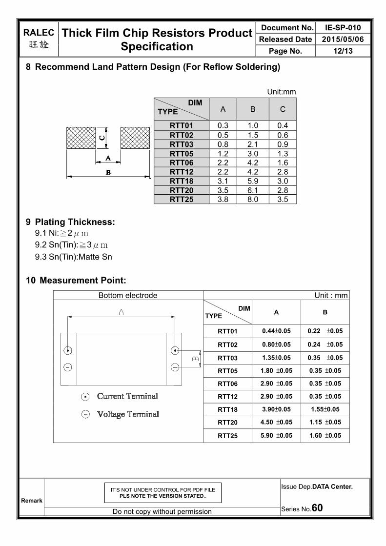
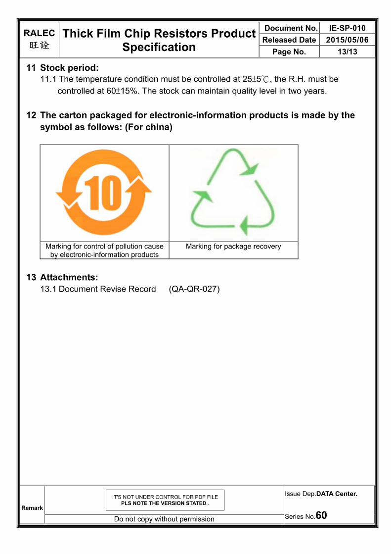
8 Recommend Land Pattern Design (For Reflow Soldering)