Rapid prototyping of multi-scale biomedical microdevices by combining additive manufacturing technologies Stefan Hengsbach & Andrés Díaz Lantada # Springer Science+Business Media New York 2014 Abstract The possibility of designing and manufacturing biomedical microdevices with multiple length-scale geome- tries can help to promote special interactions both with their environment and with surrounding biological systems. These interactions aim to enhance biocompatibility and overall per- formance by using biomimetic approaches. In this paper, we present a design and manufacturing procedure for obtaining multi-scale biomedical microsystems based on the combina- tion of two additive manufacturing processes: a conventional laser writer to manufacture the overall device structure, and a direct-laser writer based on two-photon polymerization to yield finer details. The process excels for its versatility, accu- racy and manufacturing speed and allows for the manufacture of microsystems and implants with overall sizes up to several millimeters and with details down to sub-micrometric struc- tures. As an application example we have focused on manufacturing a biomedical microsystem to analyze the im- pact of microtextured surfaces on cell motility. This process yielded a relevant increase in precision and manufacturing speed when compared with more conventional rapid prototyping procedures. Keywords Fractals . Surface topography . Material texture . Materials design . Computer-aided design . Additive manufacturing . Direct laser writing 1 Introduction Biomedical devices that include geometries and functions on multiple length scales and at different locations are able to interact with their environment and surrounding living sys- tems in a more controlled and accurate way. Multi-scale biomedical devices help to promote biomimetic approaches, as living organisms also exhibit forms and functions at differ- ent scales (Place et al. 2009), thus helping to improve aspects such as biocompatibility and overall performance. Therefore, progressive research into design and manufacturing strategies that promote hierarchical materials and structures and their integration into complex appliances is helping to improve both the diagnostic and therapeutic results of several biodevices. In biomedical sciences, fields such as prosthetics (Ponche et al. 2010; Anselme et al. 2010), health-monitoring and diagnosis (Reljin & Reljin 2002), tissue engineering (Hosseinkhani et al. 2010; Hosseinkhani et al. 2007) and even biofabrication (Borchers et al. 2012) are already starting to take advantage of multi-scale approaches, the applications of which are continuously evolving. Directly related to the concept of multi-scale geome- tries, material surface topography has an extraordinary influence on several relevant properties linked to final material (and device) performance. These properties in- clude friction coefficient (Archard 1974), wear resistance (Bushan et al. 1995), self-cleaning ability (Barthlott & Neinhuis 1997), biocompatibility (Buxboim & Discher 2010), optical response (Berginski et al. 2007), touch perception, overall aesthetic aspect and even flavor (Briones et al. 2006), to cite just a few. Thus, topography also plays a determinant role in material selection in engineering design, especially in the field of micro and nanosystem development for biomedical engineering, where the effects of topography on the incorporation of advanced properties are even more remarkable. S. Hengsbach Institute of Microstructure Technology, Karlsruhe Institute of Technology (KIT), Hermann-von-Helmholtz-Platz 1, 76344 Eggenstein-Leopoldshafen, Germany A. D. Lantada (*) Product Development Laboratory, Mechanical Engineering & Manufacturing Department, Universidad Politécnica de Madrid (UPM), José Gutiérrez Abascal, 28006 Madrid, Spain e-mail: [email protected]Biomed Microdevices DOI 10.1007/s10544-014-9864-2
Transcript
Rapid prototyping of multi-scale biomedical microdevicesby combining additive manufacturing technologies
Stefan Hengsbach & Andrés Díaz Lantada
# Springer Science+Business Media New York 2014
Abstract The possibility of designing and manufacturingbiomedical microdevices with multiple length-scale geome-tries can help to promote special interactions both with theirenvironment and with surrounding biological systems. Theseinteractions aim to enhance biocompatibility and overall per-formance by using biomimetic approaches. In this paper, wepresent a design and manufacturing procedure for obtainingmulti-scale biomedical microsystems based on the combina-tion of two additive manufacturing processes: a conventionallaser writer to manufacture the overall device structure, and adirect-laser writer based on two-photon polymerization toyield finer details. The process excels for its versatility, accu-racy and manufacturing speed and allows for the manufactureof microsystems and implants with overall sizes up to severalmillimeters and with details down to sub-micrometric struc-tures. As an application example we have focused onmanufacturing a biomedical microsystem to analyze the im-pact of microtextured surfaces on cell motility. This processyielded a relevant increase in precision and manufacturingspeed when compared with more conventional rapidprototyping procedures.
Biomedical devices that include geometries and functions onmultiple length scales and at different locations are able tointeract with their environment and surrounding living sys-tems in a more controlled and accurate way. Multi-scalebiomedical devices help to promote biomimetic approaches,as living organisms also exhibit forms and functions at differ-ent scales (Place et al. 2009), thus helping to improve aspectssuch as biocompatibility and overall performance. Therefore,progressive research into design and manufacturing strategiesthat promote hierarchical materials and structures and theirintegration into complex appliances is helping to improveboth the diagnostic and therapeutic results of severalbiodevices. In biomedical sciences, fields such as prosthetics(Ponche et al. 2010; Anselme et al. 2010), health-monitoringand diagnosis (Reljin & Reljin 2002), tissue engineering(Hosseinkhani et al. 2010; Hosseinkhani et al. 2007) and evenbiofabrication (Borchers et al. 2012) are already starting totake advantage of multi-scale approaches, the applications ofwhich are continuously evolving.
Directly related to the concept of multi-scale geome-tries, material surface topography has an extraordinaryinfluence on several relevant properties linked to finalmaterial (and device) performance. These properties in-clude friction coefficient (Archard 1974), wear resistance(Bushan et al. 1995), self-cleaning ability (Barthlott &Neinhuis 1997), biocompatibility (Buxboim & Discher2010), optical response (Berginski et al. 2007), touchperception, overall aesthetic aspect and even flavor(Briones et al. 2006), to cite just a few. Thus, topographyalso plays a determinant role in material selection inengineering design, especially in the field of micro andnanosystem development for biomedical engineering,where the effects of topography on the incorporation ofadvanced properties are even more remarkable.
S. HengsbachInstitute of Microstructure Technology, Karlsruhe Institute ofTechnology (KIT), Hermann-von-Helmholtz-Platz 1,76344 Eggenstein-Leopoldshafen, Germany
A. D. Lantada (*)Product Development Laboratory, Mechanical Engineering &Manufacturing Department, Universidad Politécnica de Madrid(UPM), José Gutiérrez Abascal, 28006 Madrid, Spaine-mail: [email protected]
Biomed MicrodevicesDOI 10.1007/s10544-014-9864-2
Normally, material surface topography is a consequence ofa material’s natural state. It can also be the result of machiningprocesses, chemical attacks or post-processes used to manu-facture a device or product. Several strategies for modifyingmaterial topographies and surface properties (towards hierar-chical materials, structures and multi-scale devices) have tak-en advantage of conventional surface micromachining(Madou 2002), laser ablation (Chandra et al. 2010),micromolding (Martin & Aksay 2005), biomimetictemplating (Pulsifier & Lakhtakia 2011), physical and chem-ical vapor deposition processes (Kwasny 2009), sol–gel pro-cedures (Jedlicka et al. 2007) and molecular self-assembly(Rahmawan et al. 2013). All these processes require enormoushands-on expertise and the final result depends on severalcontrol parameters whose interdependencies are normallycomplex to understand, characterize, model and master(Gad-el-Hak 2003). As can be seen from the previously citeddocuments, top-down and bottom-up approaches forcontrolling surface properties co-exist and in many casescomplement each other (Naik et al. 2009). The formerare more focused on mass-production (as they are de-rived from the microelectronic industry), while the latterprovide remarkable geometric versatility.
Combinations of top-down and bottom-up approaches arefrequent and have usually focused onmanufacturing the largermicrometric features by means of top-down processes(micromachining, etching, etc.). The smaller nanometric de-tails, such as for the rapid prototyping of patterned functionalnanostructures (Fan et al. 2000), are made using bottom-uptechniques (like CVD, PVD, sol–gel, self-assembly, ink-jetprinting). Normally these combinations are not aimed atobtaining 3D features at different scales, but at incorporatingsome surface patterns, 2D ½ geometries or some sort ofphysical-chemical functionality, such as enhancing bio-compatibility and implementing special actuating-sensingfunctions.
Currently, advances in computer-aided design and in high-precision additive manufacturing technologies based on layer-by-layer deposition or construction are opening new horizonsfor controlling surface topography. They are being used fromthe design stage and can be applied in a manner that is verydirect, rapid and simple. This is enabling the prototyping ofmulti-scale designs and hierarchical structures. Even thoughconventional computer-aided design packages are only capa-ble of handling Euclidean geometries and mainly rely onsimple operations (sketch based operations, extrusions, pads,holes, circular grooves, etc.) for obtaining “soft” solids andsurfaces, recent approaches relying on the use of matrix-basedprogramming have already proved to be useful for designingrough surfaces and textured objects adequately described byfractal geometries (Mandelbrot 1982a; Falconer 2003a). Inparallel, the continued progress in additive manufacturingtechnologies (also called “solid free-form fabrication” due to
the complex geometries attainable), especially during the lastdecade, has increased the range of materials capable of beingadditively processed and greatly promoted their precision,even down to nanometric features. This has implications inthe development of advanced materials and metamaterials,many of which benefit from multi-scale approaches(Bückmann et al. 2012; Röhrig et al. 2012).
Ultra-high precision additive manufacturing technologies,however, mainly direct-laser writing based on two-photonpolymerization, despite being capable of yielding nanometricdetails, are very slow and the attainable devices are normallysmaller than 1 mm3. Such tiny devices are normally aimed atvery specific studies (i.e. single-cell mechanical-biologicalexperiments). Obtaining successful implants, as well aseasy-to-handle microsystems, is still challenging since mostbiodevices and medical appliances, either for diagnostic or fortherapeutic tasks, are at least several mm3. On the other hand,industrial rapid prototyping (i.e. laser stereolithography,digital-light processing and selective laser sintering), in spiteof being fast and capable of yielding larger devices, is limitedtomanufacturing precisions typically in the 50–250μm range.It is thus still unable to produce biomedical microdevices withad hoc features for interacting at the molecular or even cellularlevel.
In this paper, we present a design and manufacturing pro-cedure for obtaining multi-scale biomedical microsystems thatis based on the combination of two additive manufacturingprocesses: a conventional laser writer to manufacture theoverall device structure, and a direct-laser writer based ontwo-photon polymerization to yield the smallest details. Theprocess stands out for its versatility, accuracy and manufactur-ing speed and allows for the manufacture of microsystems andimplants with overall sizes up to several millimeters and withdetails down to sub-micrometric structures. The followingsection explains the methods and materials used. We thenpresent our main results, propose some future directions anddetail our concluding remarks.
2 Materials and methods
2.1 Design process
As application example we have selected a biomedicalmicrosystem aimed at addressing the influence ofmicrotextures on cell motility. The system includes twomicrochambers connected by several microchannels to guidecell movement, each with a different texture at its bottom. Thecell motility experiment should begin adding cells to one ofthe chambers and growth factors to the other one, so as topromote cell movement from one chamber to another.
The design presented here is inspired by existing devices(Díaz 2013), though it has been adapted to scales better suited
Biomed Microdevices
to interacting at a cellular level. Previous designs and proto-types included 300-μmwide and 3-mm long channels andweremanufactured using conventional digital light processing. Fig-ure 1 shows the matrix-based design (see description below) ofmicrotextured channels, with the aforementioned preliminaryrapid prototype obtained by digital light processing, and cellculture results that exhibit adequate attachment of cells within atextured channel. One of the main limitations of this prelimi-nary device is that the microchannels are too wide for adequateassessment of cell motility, since several cells can enter the
channel at once. In addition, the microtextures attainable byconventional rapid prototyping have a typical height of 50–250μm, what is not perceived by single cells as a real texture.
For more adequate interactions at a cellular level, 30-μmwide channels and 1–5 μm high textures, similar to the di-mensions of pseudopods and cytoplasmatic deformations,would be advisable. At the same time, the overall device sizecannot be importantly reduced if it is to remain manipulable.Fulfilling both requirements suggests a multi-scale approach,as we will attempt to explain further on. This approach usesone technology and related material tomanufacture the overallstructure, and another technology and related material for thesmallest details.
The design process, then, also includes combinations ofdifferent processes. First, the overall structure, which mainlycomprises the different walls of the two circularmicrochambers and the six microchannels, is designed usingconventional 3D computer-aided design methods. The CADfiles can be converted into .stl (standard tessellation language)format, currently the most common file type used in 3Dadditive manufacturing. Different technologies including asdigital light processing, conventional laser stereolithography,selective laser sintering or melting and fused depositionmodeling allow .stl file as information input. The specificmethod chosen would depend on the desired material andprecision (in our case we used a Heidelberg InstrumentsDWL66fs laserwriter). There is also the possibility ofconverting the 3D design into a black-white mask for 2D½manufacture of the overall structure using lithographic ap-proaches typical to the electronic industry.
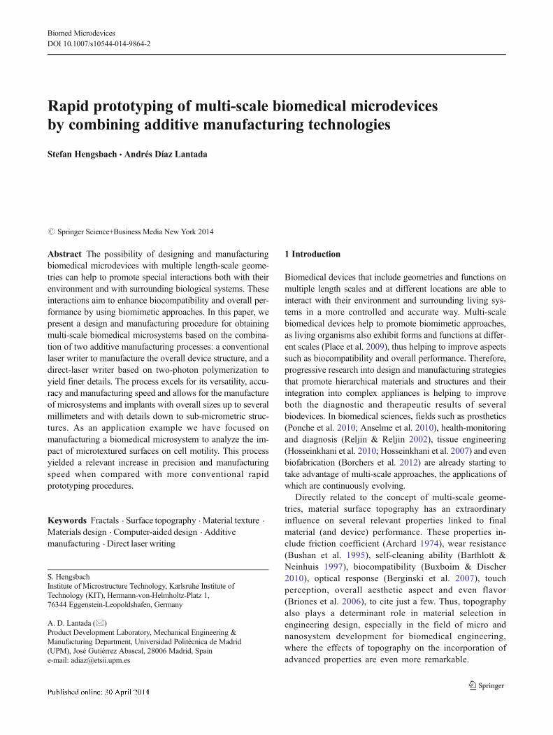
Subsequently, to incorporate the desired high-precisionmicrotextures (capable of interacting at a cellular level), addi-tional design operations rely on the generation of simplegeometries via matrix-based approaches. In such matrix-based designs the geometries are stored in the form of [X, Y,Z (x, y)] matrices, where X and Yare column vectors with thex and y components of the working grid, and Z (x, y) is acolumn vector whose components are the height values foreach (x, y) couple (spherical and cylindrical coordinates canbe used for the cases of spherical and cylindrical meshes).Then, fractal features can be introduced to incorporate con-trolled random textures to the initially regular meshes (z0), aspreviously detailed (Díaz Lantada et al. 2010). In this paperwe use fractional Brownian surface models (Mandelbrot1982b; Falconer 2003b) to incorporate the desired heightfluctuations by means of the following equation:
The models use several random functions (Ak, Bk, Ck) andcontrol constants (λ, α, m), and an initial height function “z0”can also be introduced. It is interesting to note that in fractional
Fig 1 Matrix-based design of microtextured channels. Rapid prototypeobtained by digital-light processing and results from cell culture, showingadequate attachment of cells within a textured channel. Adapted from: A.Díaz Lantada, Handbook on advanced design and manufacturing tech-nologies for biomedical devices, Springer, 2013
Biomed Microdevices
Brownian models (Mandelbrot 1982b; Falconer 2003b), thefractal dimension can be related to the exponent α, where D=3 - α, with 0<α<1. Therefore, higher values of “alfa” lead tomore “planar” surfaces or textures and lower values of “alfa”lead tomore “three-dimensional” or spiky surfaces or textures,as shown in Figs. 1a and 2b. Adequately assessing the mostbeneficial values of “alfa” for different applications is still amatter of research; for instance, our team has addressed itsimpact on cell culture (Díaz Lantada et al. 2011). By truncat-ing the aforementioned sum of infinite terms, basic fractalgeometries can be obtained in matrix form and further con-verted into recognizable CAD formats, typically .stl (standardtessellation language) .igs (initial graphics exchange specifi-cation) or .dxf (drawing exchange format). In our case thesurface generation has been programmed using Matlab (TheMathworks Inc.). The use of additional “mesh to solid” con-verters leads to the final solid files, which can be used asnormal CAD parts for further design, simulation, modelingand computer-aided manufacturing tasks. The process can beadapted to the surfaces of any computer-aided designed im-plant and multi-scale designs are possible, normally using
conventional Euclidean surfaces for micrometric – milimetricfeatures. The fractal term would usually be added for the100 nm – 10 μm range, in order to promote interactions atcellular level.
One problem associated with incorporating micrometrictextures and microstructures to computer-aided designs in-volves the final file size. For instance, a micrometric grid of300 ×300 points with a clearance between points of 1 μmleads to a .stl file of around 7 MB and to a .dxf file of around30 MB. For a useful part measuring several mm3, the incor-poration of a micrometric texture can result in file sizes ofseveral hundred MB or even a few GB, which is currentlyvery difficult to manage with computer-aided designresources.
The fact is that the “universal” .stl, .igs, .dxf and otherformats are not optimal, especially for fractal-based designs,which can be described and programmed with just one line ofcode. For instance a binary .stl file, similar to those we haveused, has typically an 80 character header (generally ignored,but which should not begin with the word “solid” because thatwill lead most software to assume that it is an ASCII .stl file).
Fig 2 a Microtextures as linessupported by pillars, asdetermined by the manufacturingtechnology. b Overview of thedifferent microtextures designedfor the channels in themicrosystem
Biomed Microdevices
Following the header, a 4 byte unsigned integer indicates thenumber of triangular facets in the file. After that integer, eachtriangle is described by twelve 32-bit-floating point numbers:three for the normal vector and then three for the Cartesiancoordinates of each vertex. In consequence, a vertex commonto four triangles of the surface is repeated four times in the .stlstructure and such description is not optimal. The convention-al CAD geometrical description of these designs unnecessar-ily increases file size. The shift to an algorithmic, rather thandescriptive, geometry is a key factor to promote materialproperties and structure by design and to the further applica-tion of these knowledge-based materials to product develop-ment (Lipson 2012).
Even though CAD resources can be utilized to almostdirectly convert the surfaces generated into solid .stl files, anysubsequent slicing of the geometry (a typical operation of thesoftware used to control layer-by-layer manufacturing ma-chines) leads to very slow and expensive manufacturing pro-cesses. In our case, a microtextured surface created on 30×300 μm2 channels in which points on the grid are separatedby 1 μm, once converted into a solid and sliced, leads to amanufacturing time ofmore than 50 h using direct laser writing.
In addition, the resist and direct laser writing process usedin this study require a distance between parallel written(polymerized) lines of 250 nm, meaning the initial matrix-based design (Fig. 1a) has to be adapted to the manufacturingprocess. Using a square grid (for each channel) of 30×300 μm2, in which the grid points are separated by 1 μm,the fractal surfaces are generated again and stored in matrixform. Each matrix is completed, as shown schematically inFig. 2a, by incorporating additional column vectors that storeinterpolated paths, separated by 250 nm, between the originalvectors separated by 1 μm. Vertical parallel lines, also sepa-rated by 250 nm, are generated under each fractal path so as toprovide a supporting structure for surface construction.
The design shown in Fig. 2b can be manufactured in just acouple of hours. This is an increase in production speed ofmorethan one order of magnitude when compared with the initialsolid model. Material and laser power consumption are alsoreduced by a similar rate. The time and material saved can beused to manufacture several prototypes so as to methodicallycompare the effects of different control parameters, such asfractal dimension, laser power used, pre-polymer employed orpost-processing operations. These can include the use of criticalpoint dryers or additional post-curing so as to precisely adjustthe prototypes to the final production stage. Additional detailsregarding the manufacturing process are included below.
2.2 Manufacturing process
Materials: For the initial stage in which the overall structure ofthe microdevices is manufactured, we used SU-8 spin coatedon a silicon wafer. SU-8 (MicroChem Corp.) is a commonly
used epoxy-based negative photoresist. It is highly functional,optically transparent and photo imageable to near UV(365 nm) radiation. Cured films or microstructures are veryresistant to solvents, acids and bases and have excellentthermal and mechanical stability. They are also importantfor the promotion of medical applications and studies inthe field of tissue repair and engineering (White R. SU-8Photoresist processing: Standard operating procedure.(Online), January, 19 2012).
For the detailed microtextures within the different chan-nels, a resist with a much lower voxel size than that of the SU-8 is needed. In our case, the resist is also linked to the two-photon polymerization process used. In this study we used theIP-Dip resist (NanoScribe GmbH and related data sheets foradditional information), a specially designed photoresist thatguarantees ideal focusing and has the highest resolution of anyNanoScribe IP-Photoresist (with feature sizes down to 150 nmand minimized shrinkage). This is because its refractive indexis matched to the focusing optic (Bückmann et al. 2012).
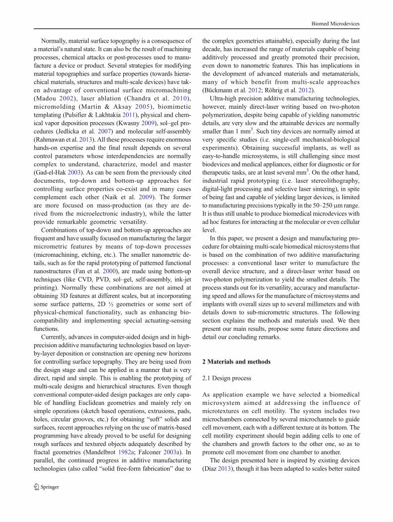
Process: The multi-scale manufacturing process followedis schematically described in Fig. 3 and consists mainly of thefollowing stages. First, a silicon wafer is spin coated with SU-8 and the overall structure of the microsystem is obtained afterphotopolymerization (using a Heidelberg InstrumentsDWL66fs laserwriter) and further development. Subsequent-ly, the channels are filled with the IP-Dip photoresist and themicrotextures are obtained using the Photonic ProfessionalSystem from NanoScribe GmbH, the first commercial directlaser writing system based on two-photon polymerization.NanoScribe GmbH (www.nanoscribe.de) was founded in2007 by scientists in the field of photonics as a spin-off com-pany of the Karlsruhe Institute of Technology (www.kit.edu).The company specializes in the innovative technique of 3Dlaser lithography and produces compact and easy-to-operatetable-top laser lithography systems (Photonic Professional).Final super critical drying and development lead to the desiredmulti-scaled microsystem.
The direct laser writing process is noted for its accuracyand versatility, since several resists and even polymer-ceramicmixtures can be manufactured. This process can also be usedadditively without the need for supporting structures, whichallows for the manufacture of especially complex parts withinner details. In short, when focused onto the volume of aphotosensitive material, the laser pulses initiate two-photonpolymerization via two-photon absorption and subsequentpolymerization, normally perceived as a change of resistviscosity. Polymerization only occurs at the focal point, wherethe intensity of the absorbed light is highest, thus enhancingthe accuracy. After illumination of the desired structures insidethe resist volume and final development (washing out of thenon-illuminated regions) the polymerized material remains inthe written 3D form (Ostendorf & Chichkov 2006;Hermatsweiler 2013).
It is important to note that the NanoScribe direct laserwriting technology writes the structures differently than con-ventional additive or “layer by layer” manufacturing technol-ogies. In other additive technologies, such as normal laserstereolithography, selective laser sintering or melting or ink-jet printing, the manufacturing process starts from a 3Dcomputer-aided design file, which is sliced into layers withthe help of ad hoc software. Then, the manufacturing isaccomplished layer by layer, by photopolimerization or depo-sition of material along the boundaries of each layer andsubsequent filling of layers with parallel lines of material. Inthe NanoScribe process, the structures are not written layer-by-layer, but by following three-dimensional paths connected
from the beginning to the end of the writing process. Thismeans that additional programming is usually needed to con-vert the original CAD files into writable structures, as alreadyschematized in Fig. 2. In addition, it is important to establishan adequate writing strategy in order to avoid writing throughalready polymerized resist. This can lead to unwanted opticaleffects because the polymerized resist has a different refractiveindex when compared to the unexposed resist.
As mentioned earlier, Matlab (TheMathworks Inc.) is usedto create the structures and also to create the informationexchange files that can be used directly in Nanoscribe Pho-tonic Professional. The advantage over using more conven-tional additive-manufacturing slicing software is that the
Fig. 3 Schematic depiction of themulti-scale rapid prototypingprocess
Biomed Microdevices
structure can be calculated and optimized based on the writingstrategy and taking into account energy and time savingissues. Time can be saved by wiring lines in the correct order.Another advantage is that additional control variables can beused and parameter variation can be easily promoted bywriting ad hoc programs. Parameter variation (i.e. distancebetween lines, structure scales, etc.) is especially useful forsystematic research and matrix-based designs are helpful forproviding this versatility and freedom of design. Finally, com-plex mathematical variables can be used to create complexstructures, in keeping with recent tendencies intended to min-imize .stl file size by resorting to algorithmic approaches(Lipson 2012).
The choice of laser power depends on the material beingprocessed and has a direct influence on the attainable voxel(here defined as the minimal building block in additive man-ufacture approaches) size. Lower powers lead to smaller voxelsizes, although to start the polymerization at one point, aminimum threshold has to be overcome. This threshold isthe minimum laser power that promotes enough energy den-sity at the focal point to start polymerization. Below thatpower, the possibility of two photons being absorbed at thefocus point is too low. If the density at the focal point is toohigh, inner explosions in the resist occur. In our case, for thefractal structures a minimal possible laser power of 5.5 mWwas chosen to create a very detailed surface. At optimalconditions a line width of 150 nm at an aspect ratio of 3.5can be reached.
One of the major problems in lithography involves shrink-ing, which affects the accuracy. There are two types of shrink,one linked to the material being processed and one linked tothe structure geometry. The former depends on the contractil-ity of the material being processed, and the latter is related topossible structure contractions and collapse during the manu-facture and subsequent development. There are also possibleadhesion effects.
Another limiting factor for some applications is the diffi-culty indirectly processing metals through direct laser writing.However, it is important to note that organic photoresists, likeSU-8 (MicroChem Corp.) or the IP-Photoresists (NanoScribeGmbH), hybrid materials, such as the Ormocere® organic–inorganic hybrid polymer family (Fraunhofer-Gesellschaft e.V.), and the amorphous semiconductor As2S3 are capable oftwo-photon polymerization, which provides a wide range ofpossibilities. In addition, through CVD/PVD coating process-es, or just by electroplating, final metallization is possible andcasting processes can also be used for additional versatility.Moreover, advanced research groups, as well as companies,are focusing on the continuous development of novel mate-rials, including photoelastomers, photopolymers and polymer-ceramic composites. These materials, even when used formedical applications, can be structured by means of directlaser writing (Ostendorf & Chichkov 2006).
3 Results
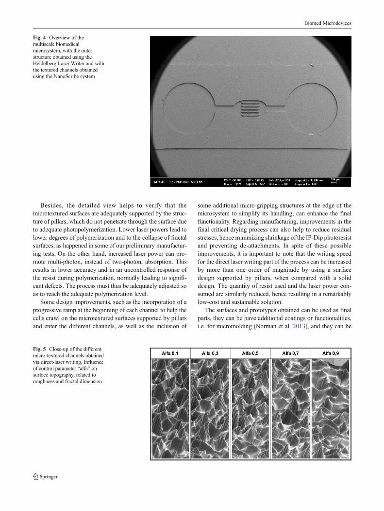
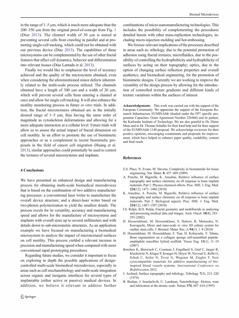
Figure 4 shows the final multiscale biomedical microsystemfor assessing the effect of surface texture on cell motility. Itsouter structure (circular chambers and channel walls) wasobtained using the Heidelberg Laser Writer, and the texturedchannels were created using the NanoScribe system. Figure 5shows several details from the different micro-textured chan-nels obtained via direct-laser writing and helps to highlight theinfluence of control parameter “alfa” on surface topography.This parameter is linked to roughness and fractal dimension.In short, higher values of “alfa” lead to more planar surfacesand lower values of “alfa” lead to more spiky surfaces. In ourcase we used a different value of “alfa” for each channel so asto control the textures of the different channels from the design(Fig. 2b) stage. Figure 5 shows the different values of “alfa”used: 0.1; 0.3; 0.5; 0.7 & 0.9, with related fractal dimensionsof 2.9; 2.7; 2.5; 2.3 & 2.1. An additional planar (with fractaldimension equal 2) was also included for use as a controlchannel in forthcoming in vitro trials.
The detailed images included in Figs. 5 and 6a help to showthe accuracy of the micro-texturing process. The similaritybetween the initial design and the final prototype validates theproposed approach for controlling surface topography inmicrosystems. It is interesting to note that the typical “steps”that can be seen in several additive manufactured deviceswhen using more conventional technologies, cannot be appre-ciated here. This is because the NanoScribe process does notwork using a sliced CAD file, but by writing lines in three-dimensional space (in a similar way as schematically depictedin Fig. 2a). Consequently, the process is additive but not “layerby layer”: instead of appreciating the different slices and steps,several lines can be perceived upon the different surfaces,according to the different paths followed by the laser. In anycase, for the purpose of the microsystem, these lines do notaffect the functionality as much as the layered and steppedgeometries usually obtained by other high-precision rapidprototyping technologies, including digital-light processingand micro-stereolithography.
The detailed image in Fig. 6b shows the fractalsurface and supporting pillars obtained by two-photonpolymerization of the previously rapid manufacturedmicrosystem structure of channels and chambers, whichshows the benefits of combining processes and materialstowards multi-scale microsystems. Some shrinking dur-ing the critical drying process (around 4 %) is presentand has led to some de-attachment between themicrotextured surfaces and the channel walls. Thisshrinking can be reduced to values of around 1-2 %by incorporating some additional outer pillars connectedto the surface. These pillars act as support structuresand absorb stress, as previous research has shown(Norman et al. 2013).
Biomed Microdevices
Besides, the detailed view helps to verify that themicrotextured surfaces are adequately supported by the struc-ture of pillars, which do not penetrate through the surface dueto adequate photopolymerization. Lower laser powers lead tolower degrees of polymerization and to the collapse of fractalsurfaces, as happened in some of our preliminary manufactur-ing tests. On the other hand, increased laser power can pro-mote multi-photon, instead of two-photon, absorption. Thisresults in lower accuracy and in an uncontrolled response ofthe resist during polymerization, normally leading to signifi-cant defects. The process must thus be adequately adjusted soas to reach the adequate polymerization level.
Some design improvements, such as the incorporation of aprogressive ramp at the beginning of each channel to help thecells crawl on the microtextured surfaces supported by pillarsand enter the different channels, as well as the inclusion of
some additional micro-gripping structures at the edge of themicrosystem to simplify its handling, can enhance the finalfunctionality. Regarding manufacturing, improvements in thefinal critical drying process can also help to reduce residualstresses, hence minimizing shrinkage of the IP-Dip photoresistand preventing de-attachments. In spite of these possibleimprovements, it is important to note that the writing speedfor the direct laser writing part of the process can be increasedby more than one order of magnitude by using a surfacedesign supported by pillars, when compared with a soliddesign. The quantity of resist used and the laser power con-sumed are similarly reduced, hence resulting in a remarkablylow-cost and sustainable solution.
The surfaces and prototypes obtained can be used as finalparts, they can be have additional coatings or functionalities,i.e. for micromolding (Norman et al. 2013), and they can be
Fig. 4 Overview of themultiscale biomedicalmicrosystem, with the outerstructure obtained using theHeidelberg Laser Writer and withthe textured channels obtainedusing the NanoScribe system
Fig. 5 Close-up of the differentmicro-textured channels obtainedvia direct-laser writing. Influenceof control parameter “alfa” onsurface topography, related toroughness and fractal dimension
Biomed Microdevices
used as green parts for obtaining replicas in other materials,depending on the application. For instance, following metallicchemical- or physical-vapor deposition to enhance surfaceconductivity, the surfaces can be electroplated with nickeland further used as inserts for injection molding of thermo-plastics or of ceramic powders with bonding agents beforefinal sintering. PDMS molds can be also directly obtained bycasting upon the surfaces and used as rapid molds for castingseveral polymers. Interesting functionalizations for furtherintegration with electronics (Simon et al. 2013) may also opennew horizons. These combinations of prototyping and mass-production processes will help to increase the range of appli-cations of these micro-textured surfaces, providing a wider
palette of materials whose surface topography can be preciselycontrolled from the design stage.
Future trials will focus on assessing the possibilities of thedesigned and manufactured microsystems by culturing realcells on them. The material is adequate for cell culture and themanufacturing precision allows for real interaction at thecellular level, as previous ground-breaking research hasshown (Klein et al. 2010). However, we still need to improvesome capabilities and resources from our labs involving mi-cromanipulation facilities, cell culture related equipment andthe cells themselves, in preparation for these trials. In any casethe device has the potential to address cell motility and theinfluence of surface topography on the cells, with roughness
Fig. 6 Close-up of the differentmicro-textured channels (upperimage) Close-up of the fractalsurface and supporting pillarsobtained by two-photonpolymerization of the previouslyrapid manufactured microsystemstructure of channels andchambers (lower image)
Biomed Microdevices
in the range of 1–5 μm,which is muchmore adequate than the200–350 μm from the original proof-of-concept from Fig. 1(Díaz 2013). The channel width of 30 μm is aimed atpreventing several cells from crawling in parallel and at pro-moting single-cell tracking, which could not be obtained withour previous device (Díaz 2013). The capabilities of thesemicrosystems can be complemented by the use of other fractalfeatures that affect cell dynamics, behavior and differentiationinto relevant tissues (Díaz Lantada et al. 2013).
Finally we would like to emphasize the level of accuracyachieved and the quality of the microsystem obtained, evenwhen considering the aforementioned minor defects inherent-ly related to the multi-scale process utilized. The channelsobtained have a length of 300 μm and a width of 30 μm,which will prevent several cells from entering a channel atonce and allow for single cell tracking. It will also enhance themotility monitoring process in future in vitro trials. In addi-tion, the fractal microtextures obtained are in the initiallydesired range of 1–5 μm, thus having the same order ofmagnitude as cytoskeleton deformations and allowing for amore adequate interaction at a cellular level. Future trials willallow us to assess the actual impact of fractal dimension oncell motility. In an effort to promote the use of biomimeticapproaches or as a complement to recent biomimetic pro-posals in the field of cancer cell migration (Huang et al.2013), similar approaches could potentially be used to controlthe textures of several microsystems and implants.
4 Conclusions
We have presented an enhanced design and manufacturingprocess for obtaining multi-scale biomedical microdevicesthat is based on the combination of two additive manufactur-ing processes: a conventional laser writer to manufacture theoverall device structure; and a direct-laser writer based ontwo-photon polymerization to yield the smallest details. Theprocess excels for its versatility, accuracy and manufacturingspeed and allows for the manufacture of microsystems andimplants with overall sizes up to several millimeters and withdetails down to sub-micrometric structures. As an applicationexample we have focused on manufacturing a biomedicalmicrosystem to analyze the impact of microtextured surfaceson cell motility. This process yielded a relevant increase inprecision and manufacturing speed when compared with moreconventional rapid prototyping procedures.
Regarding future studies, we consider it important to focuson exploring in depth the possible applications of design-controlled multi-scale biomedical microdevices, especially inareas such as cell mechanobiology and multi-scale integrationacross organic and inorganic interfaces for several types ofimplantable (either active or passive) medical devices. Inaddition, we believe it relevant to address further
combinations of micro-nanomanufacturing technologies. Thisincludes the possibility of complementing the proceduresdetailed herein with other mass-replication technologies, in-cluding micro-injection molding and hot-embossing.
We foresee relevant implications of the processes describedin areas such as: tribology, due to the potential promotion ofadhesion using fractal textures; microfluidics, due to the pos-sibility of controlling the hydrophobicity and hydrophilicity ofsurfaces by acting on their topography; optics, due to theoption of changing surface reflection properties and overallaesthetics; and biomedical engineering, for the promotion ofbiomimetic designs. Currently we are working to improve theversatility of the design process by allowing for the introduc-tion of controlled texture gradients and different kinds oftexture variations within the surfaces of interest.
Acknowledgements This work was carried out with the support of theEuropean Community. We appreciate the support of the European Re-search Infrastructure EUMINAfab (funded under the FP7 specific pro-gramme Capacities, Grant Agreement Number 226460) and its partner,the Karlsruhe Institute of Technology. We are also grateful to Dr. DieterMaas and to Dr. Thomas Schaller for their kind help and for their supportof the EUMINAfab 1140 proposal. We acknowledge reviewers for theirpositive opinions, encouraging commments and proposals for improve-ment, which have helped to enhance paper quality, readability, contentand final result.
References
E.S. Place, N. Evans, M. Stevens, Complexity in biomaterials for tissueengineering. Nat. Mater. 8, 457–469 (2009)
A. Ponche, M. Bigerelle, K. Anselme, Relative influence of surfacetopography and surface chemistry on ell response to bone implantmaterials. Part 1: Physico-chemical effects. Proc. IME. J. Eng. Med.224(12), 1471–1486 (2010)
K. Anselme, A. Ponche, M. Bigerelle, Relative influence of surfacetopography and surface chemistry on ell response to bone implantmaterials. Part 2: Biological aspects. Proc. IME. J. Eng. Med.224(12), 1487–1507 (2010)
I.S. Reljin, B.D. Reljin, Fractal geometry and multifractals in analyzingand processing medical data and images. Arch. Oncol. 10(4), 283–293 (2002)
H. Hosseinkhani, M. Hosseinkhani, S. Hattori, R. Matsuoka, N.Kawaguchi, Micro and nano-scale in vitro 3D culture system forcardiac stem cells. J. Biomed. Mater. Res. A 94(1), 1–8 (2010)
H. Hosseinkhani, M. Hosseinkhani, F. Tian, H. Kobayashi, Y. Tabata,Bone regeneration on a collagen sponge self-assembled peptide-amphiphile nanofiber hybrid scaffold. Tissue Eng. 13(1), 11–19(2007)
Borchers K, Bierwisch C, Cousteau J, Engelhard S, Graf C, Jaeger R,Klechowitz N, Kluger P, Krueger H, Meyer W, Novosel E, Refle O,Schuh C, Seiler N, Tovar G, Wegener M, Ziegler T. Newcytocompatible materials for additive manufacturing of bio-inspired blood vessels systems. International Conference onBiofabrication 2012.
J. Archard, Surface topography and tribology. Tribology 7(5), 213–220(1974)
B. Bushan, J. Israelachvili, U. Landman, Nanotribology: friction, wearand lubrication at the atomic scale. Nature 374, 607–616 (1995)
Biomed Microdevices
W. Barthlott, C. Neinhuis, Purity of the sacred lotus, or escape fromcontamination in biological surfaces. Planta 202, 1–8 (1997)
A. Buxboim, D.E. Discher, Stem cells feel the difference. Nat. Methods7(9), 695–697 (2010)
M. Berginski, J. Hüpkes, M. Schulte, G. Schöpe, H. Stiebig, B. Rech, Theeffect of front ZnO:Al surface texture and optical transparencyonefficient light trapping in silicon thin-film solar cells. J. Appl. Phys.101, 074903 (2007)
V. Briones, J.M. Aguilera, C. Brown, The effect of surface topography oncolor and gloss of chocolate samples. J. Food Eng. 77(4), 776–783(2006)
M.J. Madou, Fundamentals of microfabrication: The Science ofminiaturization, 2nd edn. (CRC Press, New York, 2002)
Chandra P, Lai K, Sunj HJ, Murthy NS, Kohn J. UV laser-ablated surfacetextures as potential regulator of cellular response. Biointerphases, 5(2), 53–59, (2010)
C.R. Martin, I.A. Aksay, Microchannel molding: A soft lithography-inspired approachto micrometer-scale patterning. J. Mater. Res.20(8), 1995–2003 (2005)
D.P. Pulsifier, A. Lakhtakia, Background and survey of bioreplicationtechniques. Bioinspir. Biomim 6(3), 031001 (2011)
W. Kwasny, Predicting properties of PVD and CVD coatings based onfractal quantitiesdescribing their surface. J. Achiev. Mater. Manuf.Eng 37(2), 125–192 (2009)
S.S. Jedlicka, J.L. McKenzie, S.L. Leavesley, K.M. Little, T.J. Webster,J.P. Robinson, D.E. Nivens, J.L. Rickus, Sol–gel derived materials assubstrates for neuronal differentiation: effects of surface features andprotein conformation. J. Mater. Chem. 16(31), 3221–3230 (2007)
Y. Rahmawan, L. Xu, S. Yang, Self-assembly of nanostructures towardstransparent, superhydrophobic surfaces. J. Mater. Chem. A 1(9),2955–2969 (2013)
M. Gad-el-Hak, The MEMS Handbook (CRC Press, New York, 2003)V.M. Naik, R. Mukherjee, A. Majumder, A. Sharma, Super functional
materials: Creation and controlof wettability, adhesion and opticaleffectsby meso-texturing of surfaces. Curr. Trends. Sci. (129–148)(2009). Platinum Jubilee Special
H. Fan, Y. Lu, A. Stump, S.T. Reed, T. Baer, R. Schunk, V. Perez-Luna,G.P. López, J. Brinker, Nature 405, 56–60 (2000)
B. Mandelbrot, The Fractal Geometry of Nature (W.H. Freeman, SanFrancisco, 1982a)
Falconer K. Fractal Geometry: Mathematical Foundations andApplications. John Wiley & Sons Ltd., 2003.
T. Bückmann, N. Stenger, M. Kadic, J. Kaschke, A. Frölich, T.Kennerknecht, C. Eberl, M. Thiel, M. Wegener, Tailored 3D
mechanical metamaterials made by dip-in direct-laser-writing opti-cal lithography. Adv. Mater. 24, 2710–2714 (2012)
M. Röhrig, M. Thiel, M. Worgull, H. Hölscher, Hierarchical structures:3D direct laser writing of nano-microstructured hierarchical gecko-mimicking surface. Small 8(19), 3009–3015 (2012)
Díaz Lantada A. Handbook on advanced design and manufacturingtechnologies for biomedical devices. Springer, 2013
A. Díaz Lantada, J.L. Endrino, A.A. Mosquera, P. Lafont, Design andrapid prototyping of DLC coated fractal surfaces for tissue engineer-ing applications. J. Phys. Conf. Ser. 252(1), 012003 (2010)
B. Mandelbrot, The Fractal Geometry of Nature (W.H. Freeman, SanFrancisco, 1982b)
Falconer K. Fractal Geometry: Mathematical Foundations andApplications. John Wiley & Sons Ltd., 2003.
A. Díaz Lantada, J. Endrino, V. Sánchez-Vaquero, A.A. Mosquera, P.Lafont Morgado, J.P. García Ruíz, Tissue engineering using novelDLC-coated rapid prototyped scaffolds. Plasma. Processes. Polym.9(1), 98–107 (2011)
H. Lipson, Frontiers in additive manufacturing, the shape of things tocome. The Bridge 42(1), 5–12 (2012)
White R. SU-8 Photoresist processing: Standard operating procedure.(Online), January, 19, 2012.
A. Ostendorf, B.N. Chichkov, Two-photon polymerization: A new ap-proach to micromachining. Photonics. Spectr. (October) (2006)
M. Hermatsweiler, Laserlithografie als Innovationstreiber fürSchlüsseltechnologien. Laser. Technik. J. (September) (2013)
J.J. Norman, S.O. Choi, N.T. Tong, A.R. Aiyar, S.R. Patel, M.R.Prausnitz, M.G. Allen, Hollow microneedles for intradermal injec-tion fabricated by sacrificial micromolding and selective electrode-position. Biomed. Microdevices 15(2), 203–210 (2013)
D. Simon, T. Ware, R. Marcotte, B.R. Lund, D.W. Smith, M. Di Prima,R.L. Rennaker, W. Voit, A comparison of polymer substrates forphotolithographic processing of flexible bioelectronics. Biomed.Microdevices 15(6), 925–939 (2013)
F. Klein, T. Striebel, Z. Jiang, C.M. Franz, G. Von Freymann, M.Bastmeyer, Elastic fully three-dimensional microstructure scaffoldsfor cell force measurements. Adv. Mater. 22, 868–871 (2010)
A. Díaz Lantada, B. Pareja Sánchez, C. GómezMurillo, J. Urbieta Sotillo,Fractals in tissue engineering: Towards biomimetic cell-culture ma-trices, microsystems and microstructured implants. Expert. Rev.Med. Devices. 10(5), 629–648 (2013)
Huang TQ, Qu X, Liu J, Chen S. 3D printing of biomimetic microstruc-tures for cancer cell migration. Biomedical Microdevices, DOI 10.1007/s10544-013-9812-6, (Online), October, 29, 2013.