Page 1
RC Snubber Design using Root-Loci Approach for
Synchronous Buck SMPS
by
Yen-Ming Chen
A thesis
presented to the University of Waterloo in fulfillment of the
thesis requirement for the degree of Master of Applied Science
in Electrical & Computer Engineering
Waterloo, Ontario, Canada, 2005 Yen-Ming Chen 2005
Page 2
ii
I hereby declare that I am the sole author of this thesis. This is a true copy of the thesis, including any required final revisions, as accepted by my examiners. I understand that my thesis may be made electronically available to the public.
Page 3
iii
ABSTRACT
This thesis presents an analytical approach using Root-Loci method for designing
optimum passive series RC snubbers for continuous-current synchronous buck switch mode
power supply (SMPS).
Synchronous buck SMPS is the most popular power converter topology found in modern
consumer electronics. It offers relatively good efficiency to target the high-current and low-
voltage requirements while it is also relatively inexpensive to implement.
Passive series RC snubbers are simple, efficient and cost-effective open-loop equalizer
circuit for synchronous buck SMPS. Its purpose is to control and to balance between the rate
of rise and the overshoots of transient switching waveform in order to optimize efficiency and
reliability
Existing methods of RC snubber design are solely based on second-order approximation.
It is investigated in this research that this approximation is highly inaccurate in SMPS
applications because higher order equivalent models are required for the load path of the
SMPS. The results using the RC snubbers obtained from existing method are shown to be
unsatisfactory without correlation to the calculations and simulations based on second-order
approximation. Optimum RC values obtained using Root-Loci approach presented in this
thesis are shown to correlate to both Spice simulation and lab measurements.
Page 4
iv
ACKNOWLEDGEMENTS
Pursuing this academic degree has been a lengthy journey. Over the past three and an half
years, it has been challenging to manage the contrary priorities between my full-time job and
my part-time degree, and to deliver my performance for both.
I dedicate this thesis to my lovely wife, Annie Hsing-Rou Chen, for her unconditional and
uncompromised supports and encouragements during these years. I would also like to thank
my cousin, Yen-Wen Wang, and my brother-in-law, Jay Hsin-Chieh Lu, for being the two of
the closest and most supportive family members for sharing my daily burdens so I can fully
concentrate during this difficult time.
I would also like to thanks my director, Salim Lakhani, and my manager, George Reesor,
of Board Engineering at ATI Technologies, for continuously having confidence in me and for
their supports with vision which fulfils both my career and my academic goals. I also thank
my friends, Jian Li and Nino Zahirovic for many valuable technical discussions related to this
research topic.
Last and most importantly of all, I would like to express my sincere gratitude to my
supervisor Professor Safieddin Safavi-Naeini of University of Waterloo for his invaluable
guidance, advice and support throughout my postgraduate program.
Page 5
v
TO MY LOVELY WIFE
ANNIE CHEN
Page 6
vi
TABLE OF CONTENTS
ABSTRACT...........................................................................................................iii
ACKNOWLEDGMENTS.........................................................................................iv
TABLE OF CONTENTS .........................................................................................vi
LIST OF TABLES................................................................................................viii
LIST OF FIGURES ................................................................................................ix
1 INTRODUCTION .............................................................................................1
1.1 Motivations and Objectives........................................................................1
1.2 Dissertation Outline....................................................................................5
1.3 Fundamentals of Switch Mode Power Supply (SMPS) .............................7
Buck (Step-Down) SMPS .............................................................................7
Ideal Continuous-Mode Buck SMPS............................................................8
Synchronous Buck or synchronous rectification SMPS .............................12
1.4 The Potential Hazards due to Transient Switching Behaviour ................16
1.5 The Benefits of Simple Dissipative Voltage Snubber .............................19
1.6 Literature Surveys & Existing Methods of Snubber Designs ..................21
Classical Snubber Theory, Design and Application ...................................22
Optimum Snubber for Second-Order Circuit..............................................25
Second-order RC Snubber Design suggested by Industry..........................27
Snubber Design from the Lab Approach ....................................................27
2 LINEAR SECOND-ORDER SMPS LOAD-PATH APPROXIMATION...............29
2.1 N-channel MOSFET Approximation .......................................................29
High-Side NMOS (QH) ..............................................................................32
Low-Side NMOS (QL)................................................................................33
Page 7
vii
2.2 Second-Order Equivalent Circuit of Load Path .......................................34
2.3 Determining RLC Values of Second-Order Equivalent ..........................35
Obtaining from Supplier .............................................................................36
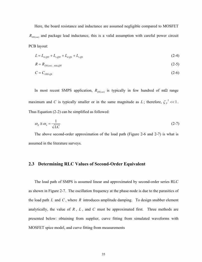
Curve Fitting from Simulated Waveform with MOSFET Spice Model.....37
Curve Fitting from Measured Waveform....................................................39
2.4 Second-Order Load Path Equivalent........................................................41
3 SECOND-ORDER SNUBBER RESISTOR DESIGN...........................................43
4 HIGHER-ORDER SNUBBER DESIGN USING ROOT-LOCI.............................47
4.1 Snubber Resistor Design Criteria.............................................................47
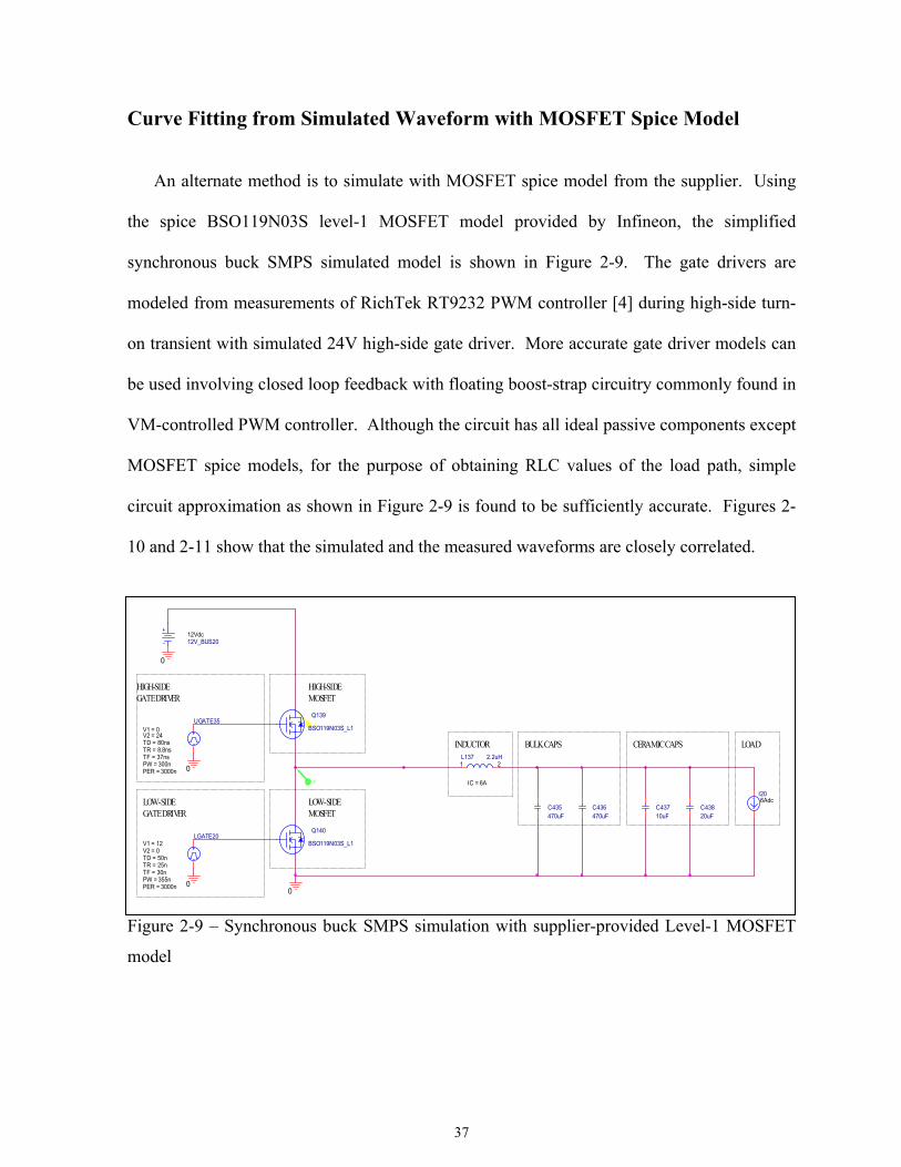
4.2 Snubber Capacitor Design Criteria ..........................................................54
4.3 Final Snubber RC Value Verification ......................................................60
4.4 Snubber Design without Snubber Resistor ..............................................61
4.5 Optimum Snubber Resistor using Maxim’s Approach ............................65
5 SNUBBER CAPACITOR BOUNDARY CRITERIA USING CIRCUIT THEORY ...66
5.1 The Upper Bound of Snubber Capacitor..................................................66
Maximum Resistive Power Dissipation......................................................68
Minimum Average Resistive Power Dissipation ........................................72
Resistive One-Time Pulse Power Dissipation ............................................72
5.2 The Lower Bound of Snubber Capacitor .................................................74
6 CONCLUSION ...............................................................................................75
REFERENCES......................................................................................................77
Page 8
viii
LIST OF TABLES Table 3-1 – Snubber Resistor Calculation for 2nd-order Approximation ............................... 44
Table 5-1 – Calculated and simulated resistor power dissipation............................................ 71
Table 5-2 – Measured temperature of snubber resistor............................................................ 72
Page 9
ix
LIST OF FIGURES
Figure 1-1 – Number of transistors in the microprocessors increases exponentially ................ 1
Figure 1-2 – CPU Current demand increases and supply voltages decrease in order to reduce
power consumption ............................................................................................................. 2
Figure 1-3 – Fundamental synchronous buck SMPS topology.................................................. 3
Figure 1-4 – Switching operation and voltage spikes of synchronous buck SMPS................... 3
Figure 1-5 – Synchronous buck SMPS with passive RC snubber circuit .................................. 4
Figure 1-6 – Basic buck SMPS concept..................................................................................... 8
Figure 1-7 – Buck SMPS operation switching waveforms........................................................ 9
Figure 1-8 – Typical Synchronous Buck SMPS Circuit .......................................................... 14
Figure 1-9 – Synchronous Buck SMPS switching waveforms without parasitics................... 15
Figure 1-10 – Synchronous buck SMPS load path current ...................................................... 16
Figure 1-11 – Synchronous Buck SMPS switching waveforms with parasitics...................... 17
Figure 1-12 – The schematic of the SMPS load path .............................................................. 18
Figure 1-13 – Second-order snubber design approach............................................................. 23
Figure 1-14 – Effect of power dissipation in Rsnubber due to Csnubber................................ 26
Figure 2-1 – General N-channel-MOSFET model .................................................................. 30
Figure 2-2 – Typical NMOS turn-on waveform ...................................................................... 31
Figure 2-3 – High-Side NMOS equivalent model during turn-on ........................................... 32
Figure 2-4 – NMOS diode recovery waveform ....................................................................... 33
Figure 2-5 – Low-Side NMOS equivalent model during High-Side NMOS turn-on.............. 33
Figure 2-6 – Equivalent circuit representing the resonance condition during switching......... 34
Figure 2-7 – Simplified second-order circuit representing the resonance condition during
switching ........................................................................................................................... 34
Figure 2-8 – Infineon BSO119N03S MOSFET datasheet figures........................................... 36
Figure 2-9 – Synchronous buck SMPS simulation with supplier-provided Level-1 MOSFET
model ................................................................................................................................. 37
Figure 2-10 – Simulated SMPS phase-node oscillation with Level-1 MOSFET model ......... 38
Page 10
x
Figure 2-11 – Measured SMPS phase-node oscillation ........................................................... 38
Figure 2-12 – Simplified second-order LC circuit................................................................... 38
Figure 2-13 – Schematic of the SMPS implementation........................................................... 40
Figure 2-14 – PCB layout of the SMPS load path snapshoot .................................................. 40
Figure 2-15 – Equivalent second-order RLC circuit representing SMPS load path................ 41
Figure 2-16 – Simulated phase-node oscillation and input current of Level-1 MOSFET model
and second-order model .................................................................................................... 42
Figure 3-1 – Second-order approach of snubber resistor ......................................................... 43
Figure 3-2 – Simulated waveform (in red) with snubber resistor of 2.32R based on 2nd-order
approximation.................................................................................................................... 44
Figure 3-3 – Simplified equivalent SMPS load path with snubber resistor............................. 45
Figure 3-4 – Second-order RLC oscillatory circuit with and without snubber resistor ........... 46
Figure 3-5 – Third-order RLC oscillatory circuit with and without snubber........................... 46
Figure 4-1 – Root-Loci of third-order approximation with changing snubber resistor ........... 48
Figure 4-2 – Root-Loci of third-order approximation with changing Rsnubber ..................... 49
Figure 4-3 – MOSFET-model Spice schematic with snubber resistor .................................... 49
Figure 4-4 – Third-order Spice schematic with snubber resistor............................................. 50
Figure 4-5 – MOSFET-model and 3rd-order simulation with snubber resistor correlated with
Root-Loci plot ................................................................................................................... 50
Figure 4-6 – Step-response comparison for various characteristic-equation-root locations in
the s-plane.......................................................................................................................... 51
Figure 4-7 – MOSFET-model simulation sweeping Rsnubber correlated with Root-Loci
predicted optimum value ................................................................................................... 53
Figure 4-8 – MOSFET-model Spice schematic with snubber resistor and capacitor .............. 54
Figure 4-9 – 4th-order Spice schematic with snubber resistor and capacitor .......................... 54
Figure 4-10 – Root-Loci of forth-order approximation with changing Csnubber with fixed
0.7Ω Rsnubber................................................................................................................... 55
Figure 4-11 – Root-Loci of forth-order approximation with changing Csnubber with fixed
0.7Ω Rsnubber (details)..................................................................................................... 57
Page 11
xi
Figure 4-12 – Measurement vs. MOSFET and forth-order simulation – 0.7Ω + 2.2nF .......... 59
Figure 4-13 – Measurement vs. MOSFET and forth-order simulation – 0.7Ω + 10nF ........... 59
Figure 4-14 – Measurement vs. MOSFET and forth-order simulation – 0.7Ω + 22nF ........... 59
Figure 4-15 – Root-Loci of 4th-order approximation with changing Rsnubber with fixed 22nF
Csnubber............................................................................................................................ 60
Figure 4-16 – Ideal and real equivalent circuit representation of SMPS load path with
Csnubber alone .................................................................................................................. 61
Figure 4-17 – Root-Loci of 3rd-order approximation with changing Csnubber without
Rsnubber............................................................................................................................ 63
Figure 4-18 – MOSFET-model Spice schematic with snubber capacitor alone...................... 63
Figure 4-19 – 3rd-order Spice schematic with snubber capacitor alone.................................. 63
Figure 4-20 – MOSFET and third-order simulation with snubber capacitor alone (unstable) 64
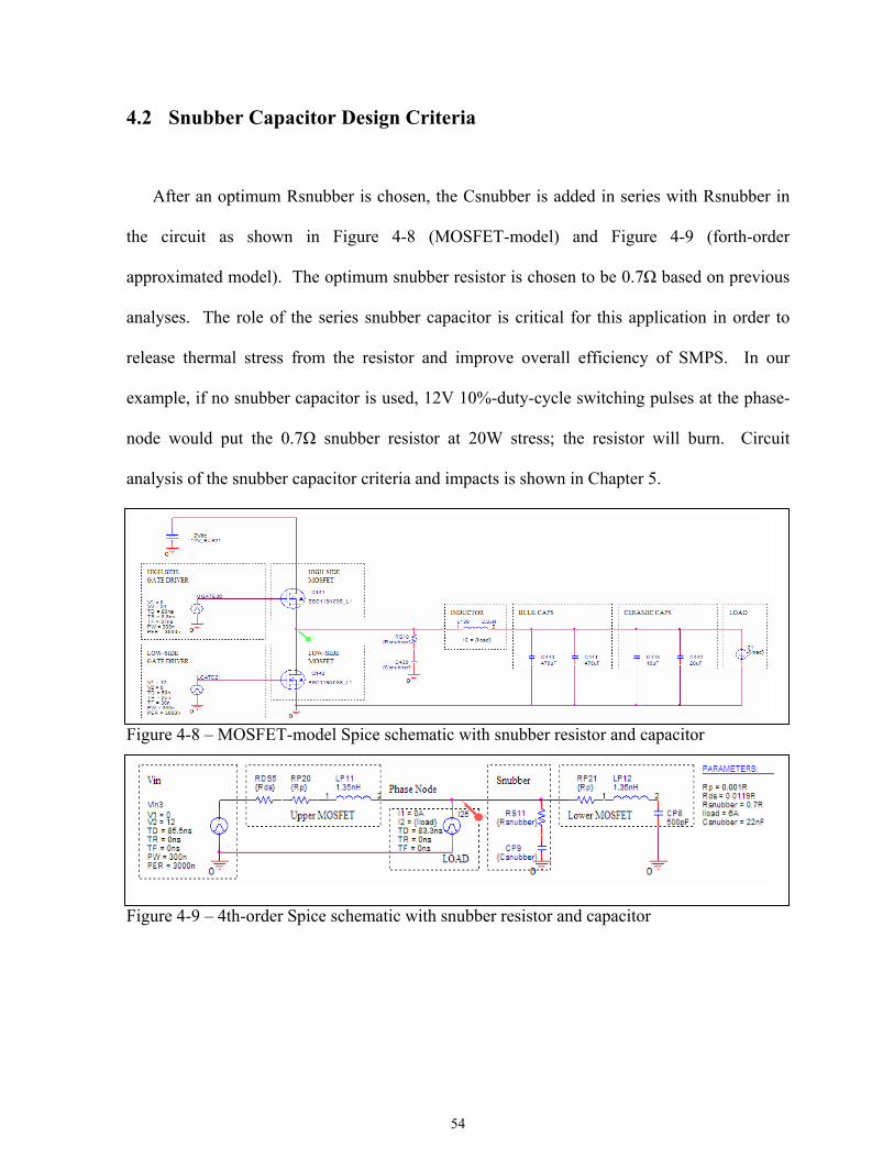
Figure 5-1 – MOSFET model simulation showing Vcsnubber waveform varying Csnubber
with 0.7Ω Rsnubber........................................................................................................... 67
Figure 5-2 – Timing for calculating maximum Rsnubber power dissipation .......................... 68
Figure 5-3 – Simulation of resistor power dissipation............................................................. 70
Figure 5-4 – Resistor pulsed power characteristic ................................................................... 73
Page 12
1
1 INTRODUCTION
1.1 Motivations and Objectives
Advances in microprocessor technology and modern electronics continue to challenge the
design of power supplies of these devices. Complying with Moore’s Law, which states that
“transistor density doubles every eighteen months” (Figure 1-1), average and dynamic current
demand and current skew rate requirement inevitability increase as number of transistor
doubles; and with smaller transistor size, voltage requirement naturally decreases in order to
reduce overall power consumption (Figure 1-2). Synchronous buck switch mode power
supply (SMPS) has therefore become the most commonly used power supply topology used
in these modern circuits, as its efficiency addresses these high-current low-voltage
requirements to deliver a cost-effective solution.
Figure 1-1 – Number of transistors in the microprocessors increases exponentially
Page 13
2
Figure 1-2 – CPU Current demand increases and supply voltages decrease in order to reduce power consumption
With the benefit synchronous buck SMPS brings alone, it has some drawbacks. Its
operation inevitably creates noises and ripples in the circuit due to switching voltage and
current, and the transient switching actions can also cause operational instability and
unreliability to the devices and to the circuit if it is improperly designed.
The fundamental synchronous buck SMPS topology is shown in Figure 1-3. The
frequency of operation and the duty-cycle of the two switches are determined by the
integrated-circuit controller based the desired output voltage and feedback. As the switches
turn on and off, pulsating voltage is created at the phase-node or the switch-node. This
voltage is then low-pass LC-filtered to create near-DC output voltage. Voltage spikes and
ringing are commonly found at the phase-node during switching as shown in Figure 1-4. This
waveform creates undesirable overshoots that can damage the controller, violate the
breakdown voltage and increase power dissipation of the switch, cause spurious turn-on due
to parasitic coupling causing shoot-through current, and create potential EMI issues.
CPU Supplied Voltage CPU Current Demand
1991 1993 1995 1997 1999 2001
Page 14
3
Figure 1-3 – Fundamental synchronous buck SMPS topology
Figure 1-4 – Switching operation and voltage spikes of synchronous buck SMPS
Swithcing Frequency and
Duty-Cycle Controller
FEEDBACK or SENSE
HIGH-SWITCH CONTROL
LOW-SWITCH CONTROL
PHASE-NODEor
SWITCH-NODE
HIGH-SIDE SWITCH
INDUCTOR
VIN
VOUT
LOADOUTPUT
CAPS
LOW-SIDE SWITCH
Page 15
4
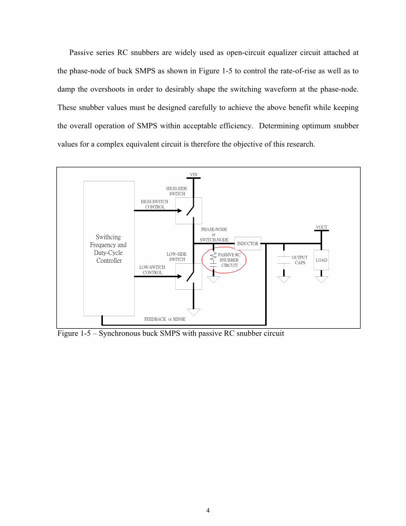
Passive series RC snubbers are widely used as open-circuit equalizer circuit attached at
the phase-node of buck SMPS as shown in Figure 1-5 to control the rate-of-rise as well as to
damp the overshoots in order to desirably shape the switching waveform at the phase-node.
These snubber values must be designed carefully to achieve the above benefit while keeping
the overall operation of SMPS within acceptable efficiency. Determining optimum snubber
values for a complex equivalent circuit is therefore the objective of this research.
Figure 1-5 – Synchronous buck SMPS with passive RC snubber circuit
Swithcing Frequency and
Duty-Cycle Controller
FEEDBACK or SENSE
HIGH-SWITCH CONTROL
LOW-SWITCH CONTROL
PHASE-NODEor
SWITCH-NODE
HIGH-SIDE SWITCH
INDUCTOR
VIN
VOUT
LOADOUTPUT
CAPS
PASSIVE RC SNUBBER CIRCUIT
LOW-SIDE SWITCH
Page 16
5
1.2 Dissertation Outline
The remaining of Chapter 1 summarizes the background of the synchronous buck SMPS
theory where the design challenges and the potential hazards due its transient switching
operation are introduced. The benefits of the added snubbers are presented, and this leads to
the introduction of the simple dissipative passive RC snubber. This snubber is most widely
applied, efficient and cost-effective solution to improve reliability of the SMPS by shaping
the transient switching waveforms. Following the SMPS introduction, the summary of
literature surveys shows that exiting RC snubber design methods assume the system with or
without added snubber can be accurately approximated by second-order equivalent circuit.
These methods are usually based on iterative measurements under the second-order
assumption, and this approximation is later shown in Chapter 3 in simulations and
measurements to be highly inaccurate for this application. Many circuits require to be
approximated with higher order equivalent circuits instead of simple second-order equivalent
circuit; the load path of the continuous-current-mode synchronous buck SMPS being the
example.
Chapter 2 justifies that the load path of the synchronous buck SMPS can be approximated
with second-order equivalent circuit. This model is required to be established first before RC
snubbers are added to the circuit. This approximation starts from the non-linear elements in
the load path during transient switching, mainly the upper and the lower MOSFETs; the
approximation of these MOSFETs to only passive linear elements is obtained based on
MOSFET physical structure and switching characteristics. The remaining of the chapter
presents three methods to obtain the value of the elements in the equivalent circuit. The
Page 17
6
simulated waveform of the final second-order equivalent circuit is shown to closely correlate
to both Spice model simulated waveform and measurements.
Chapter 3 derives the second-order approximation approach of finding optimum RC
snubbers presented in literature survey. This chapter also demonstrates that the values
obtained based on this approximation do not yield expected result for synchronous buck
SMPS. This chapter justifies and validates that the linear second-order approximation of
SMPS load path is only accurate without the snubber elements; however, this assumption
does not hold with added snubbers, hence the existing methodology is oversimplifying. A
more rigorous or higher order equivalent approximation is therefore needed for the overall
circuit after adding RC snubbers.
Chapter 4 presents an analytical design approach using Root-Loci analysis where the
optimum RC values are obtained for continuous-mode NMOS synchronous buck SMPS.
Trade-off of determining these optimum selections is discussed, and calculated values are
confirmed in simulations and measurements with good correlations.
Chapter 5 discusses some analytical methods from circuit theory which aims to determine
the boundary of RC values which are critical in practical quick design calculations.
Chapter 6 summarizes the thesis and references used within this thesis are listed at after
Chapter 6.
The proposed analytical approach is currently being applied to SMPS designs in various
consumer products in graphic board development of ATI Technologies Inc.
Page 18
7
1.3 Fundamentals of Switch Mode Power Supply (SMPS)
A switch mode power supply (SMPS) or switching regulator is a circuit that uses an
energy-storage element to transfer energy from input to output based on a control and a switch
modulation techniques. While linear power supply (or linear regulator) can only step down
from input power, the basic topologies are step up (boost), step down (buck), or invert output
voltage (fly-back) with respect to input voltage. In the thesis, only buck SMPS is discussed.
Buck (Step-Down) SMPS
The benefit of buck SMPS over linear power supply (or linear regulator) is its efficiency.
A buck SMPS achieves higher efficiency compared to linear regulator because of its
switching operation that minimizes the average input current. Linear regulator has the
average input current equal to the average output current; therefore, efficiency is lost in power
dissipation roughly equal to ( ) OUTOUTIN IVV ⋅− due to the input/output voltage drop. Its
efficiency is simply equal to the output voltage divided by the input voltage. For low-output-
voltage and high-current applications in most electronic products today, this loss is simply
unacceptable.
The drawbacks of SMPS in general are mainly the noise or ripple due to its switching
operation and the transient spikes or ringing due to circuit elements or board parasitics.
Page 19
8
The continuous-current-mode (or simply continuous-mode) buck SMPS is defined when
the output current never goes to zero; where as the discontinuous-mode SMPS has output
current reaching zero. The design of the snubber circuit presented in this thesis applies to
more commonly used continuous-mode SMPS; discontinuous-mode SMPS has additional
ringing due to current discontinuity where the effectiveness and impacts of the snubber are
not quantified in this thesis; the discontinuous operation is therefore not discussed.
Ideal Continuous-Mode Buck SMPS
The ideal buck (or step-down) SMPS is shown in Figure 1-6 [11]. It consists of the
controller integrated circuit, the switch, the inductor, the diode, and the load capacitor.
Instead of delivering the required output current from the input directly (or linearly, as the
name linear regulator derived from), an on/off switch draws the current from the input at a
certain duty cycle; the pulsating voltage produced by the switching actions is then low-pass
LC-filtered to provide near-DC output voltage with some defined acceptable ripple peak-to-
peak voltage. The benefit is the low average input current to achieve higher efficiency.
Figure 1-6 – Basic buck SMPS concept
Page 20
9
The current paths and the voltage/current waveforms of the continuous-mode operating
waveforms are shown in Figure 1-7. When the switch is on, the voltage ( )OUTIN VV − appears
across the inductor, and the inductor current increases with a slope equal to ( ) LVV OUTIN − .
When the switch turns off, the current cannot change instantaneously and continues to flow
through the inductor into the load with the ideal diode (no forward voltage drop) providing
the return current path. Therefore, the voltage across the inductor is theoretically
OUTOUT VV −=−0 and the inductor current decreases with a slope equal to LVOUT . The load
current LOADLOAD iI = in this ideal scenario is a constant current which is the summation of the
inductor current Li and the capacitor current Ci .
Figure 1-7 – Buck SMPS operation switching waveforms
There are several important idealizations on the waveforms shown in Figure 1-5. Ideal
components have been assumed, i.e., the input voltage source has zero impedance, the switch
Page 21
10
has zero on-resistance, the diode has no forward drop, and there is zero turn-on and turn-off
rise-time.
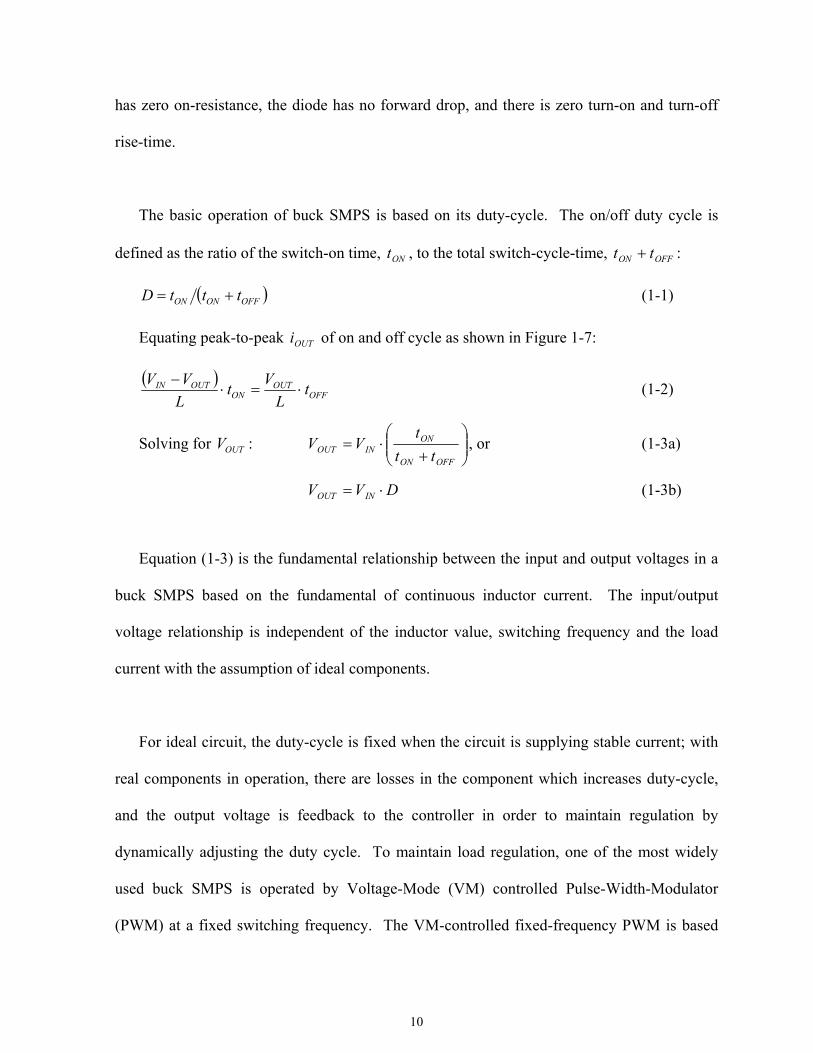
The basic operation of buck SMPS is based on its duty-cycle. The on/off duty cycle is
defined as the ratio of the switch-on time, ONt , to the total switch-cycle-time, OFFON tt + :
( )OFFONON tttD += (1-1)
Equating peak-to-peak OUTi of on and off cycle as shown in Figure 1-7:
( )OFF
OUTON
OUTIN tL
VtLVV
⋅=⋅− (1-2)
Solving for OUTV :
+
⋅=OFFON
ONINOUT tt
tVV , or (1-3a)
DVV INOUT ⋅= (1-3b)
Equation (1-3) is the fundamental relationship between the input and output voltages in a
buck SMPS based on the fundamental of continuous inductor current. The input/output
voltage relationship is independent of the inductor value, switching frequency and the load
current with the assumption of ideal components.
For ideal circuit, the duty-cycle is fixed when the circuit is supplying stable current; with
real components in operation, there are losses in the component which increases duty-cycle,
and the output voltage is feedback to the controller in order to maintain regulation by
dynamically adjusting the duty cycle. To maintain load regulation, one of the most widely
used buck SMPS is operated by Voltage-Mode (VM) controlled Pulse-Width-Modulator
(PWM) at a fixed switching frequency. The VM-controlled fixed-frequency PWM is based
Page 22
11
on an error amplifier which negatively responds to the error between the output voltage
feedback and a reference voltage. As the output voltage increases, the duty cycle decreases to
reduce output voltage; and vise-versa. The response is under the designed closed-loop
bandwidth of SMPS. With a fixed operation, the noise spectrum of PWM is relatively
narrow and the output voltage ripple can be easily maintained within the peak-to-peak
specification using simple LC low-pass filters.
The VM-mode fixed-frequency PWM operation shown above is the most popular of many
control and switch modulation techniques; therefore, it is used though out the thesis as an
example, but the design of the snubber circuit as shown in Figure 1-5 presented in this thesis
is irrelevant to the types of control and/or switch modulation technique.
In addition to the basic operation of buck SMPS shown above, there are some important
characteristics emphasized below between the average and the instantaneous input/output
current relationship which directly relates to this thesis.
The instantaneous inductor current Li is equal to the instantaneous output current OUTi ,
which is the sum of the diode Di and the switch SWi instantaneous currents. It is also
important to realize that the instantaneous input current is the switch current SWIN ii = ; this
input current is equal to the instantaneous inductor or the instantaneous output current during
the ON-time, ONt , and this input current is zero during OFF-time, OFFt , i.e.,
OUTLSWIN iiii === for ONtt = (1-4)
0=INi for OFFtt = (1-5)
Page 23
12
Although it appears to be quite obvious, Equation (1-4) is an important characteristic of
buck SMPS operation which could sometimes be overlooked or wrongly assumed to have
average input current applied instead of instantaneous input current in some calculations. The
output current is continuous, while the input current is pulsating; the average input current is
always less than the average output current; the factor is the duty-cycle D .
OUTIN II < or OUTIN IDI =⋅ (1-6)
The basic principle of any power supply is that the input power equals to the output power
times the efficiency. Equating Equations (1-3b) and (1-6), the input and output power of
SMSP is theoretically identical; therefore, the efficiency of an ideal SMPS is 100%.
Synchronous Buck or synchronous rectification SMPS
Ideal buck SMPS presented above is not physically realizable. In the real circuit, both the
switch and the diode have voltage drops across them when conducting, which creates internal
power dissipation and loss of efficiency. In practical designs, the switch is commonly
realized by a N-channel MOSFET; therefore, the overall power loss during the ON state is
partially contributed by the MOSFET conduction loss which is defined to be the average of
the instantaneous switch current SWi squared times the on resistance )(onDSR of the MOSFET
times the duty cycle D .
DRdttit
DRdttit
P ONdst
OUTON
ONdst
SWON
C
ONON
⋅⋅
=⋅⋅
= ∫∫ )(
2
)(
2
)(1)(1
DRI ONdsOUT ⋅⋅= )(2 (1-7)
Page 24
13
During the OFF state, current flowing thru the diode develops forward voltage drop which
causes the main power dissipation:
( )Ddttit
VPOFFt
OUTOFF
diodediode −⋅
⋅∆= ∫ 1)(1
( )DIV OUTdiode −⋅⋅∆= 1 (1-8)
When the duty cycle is less than 50%, which is in the case of most low-voltage SMPS
applications today because this uses the full advantage of the better efficiency SMPS delivers,
the power loss across the diode becomes significant. MOSFET technology today is capable
to achieve much lower voltage drop when operating in ohmic region with low )(onDSR
compared to the forward voltage drop of the diode. Even if Schottky diode is used, with low
voltage drop of less than 0.5V, the power loss is still much higher compared to on-resistive
drop of the MOSFET. When the diode is replaced by a MOSFET, this is the fundamental
topology of synchronous-rectifier or synchronous-switch buck SMPS.
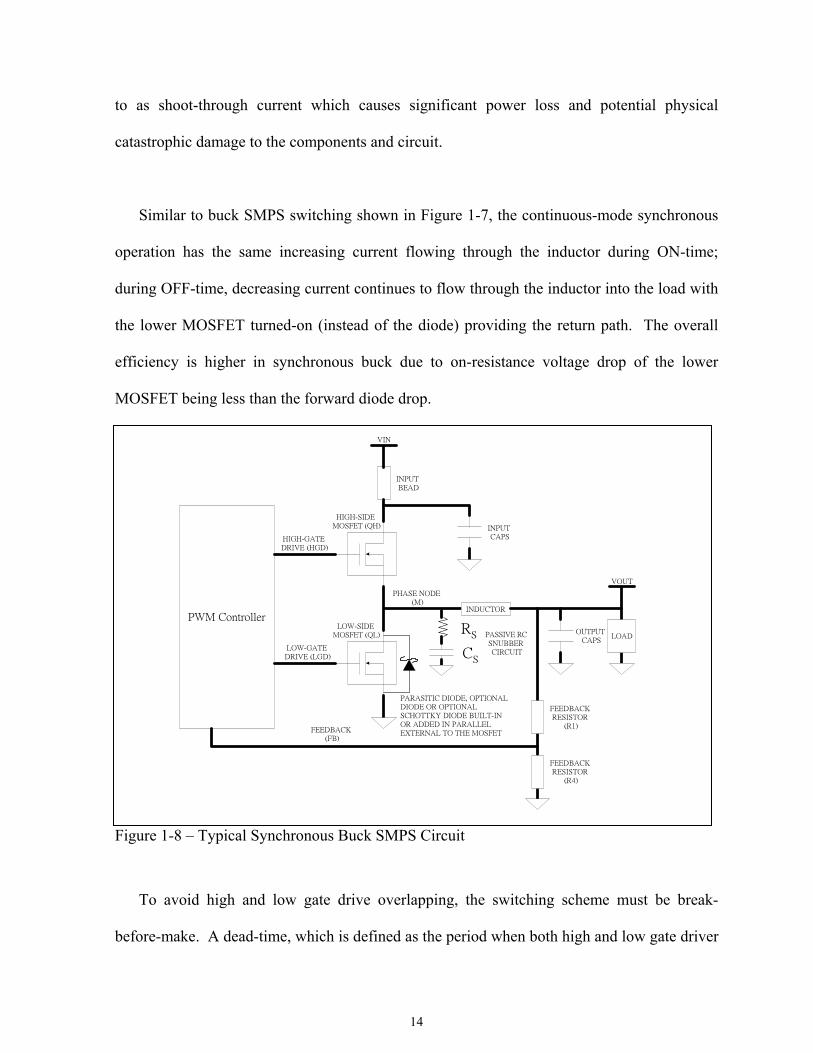
Figure 1-8 shows the typical synchronous buck SMPS circuit where the two N-channel
MOSFETs are used as switches commonly referred to Upper/High/Top-Side MOSFET and
Lower/Low/Bottom-Side MOSFET. This thesis is limited to more commonly-used NMOS-
only synchronous buck SMPS; therefore, the following discussion is limited by this
assumption. The controller shown is a VM-mode synchronous buck PWM controller which
consists of two gate drivers synchronously switching the MOSFETs. The synchronous
operation of the gate drivers must be non-overlapping to prevent cross-conduction current.
This is the event when both switches are turned-on and the current spike is typically referred
Page 25
14
to as shoot-through current which causes significant power loss and potential physical
catastrophic damage to the components and circuit.
Similar to buck SMPS switching shown in Figure 1-7, the continuous-mode synchronous
operation has the same increasing current flowing through the inductor during ON-time;
during OFF-time, decreasing current continues to flow through the inductor into the load with
the lower MOSFET turned-on (instead of the diode) providing the return path. The overall
efficiency is higher in synchronous buck due to on-resistance voltage drop of the lower
MOSFET being less than the forward diode drop.
Figure 1-8 – Typical Synchronous Buck SMPS Circuit
To avoid high and low gate drive overlapping, the switching scheme must be break-
before-make. A dead-time, which is defined as the period when both high and low gate driver
PWM Controller
FEEDBACK (FB)
HIGH-GATE DRIVE (HGD)
LOW-GATE DRIVE (LGD)
PHASE NODE (M)
HIGH-SIDE MOSFET (QH)
LOW-SIDE MOSFET (QL)
INDUCTOR
INPUT CAPS
INPUT BEAD
VIN
VOUT
LOADOUTPUT
CAPSPASSIVE RC SNUBBER CIRCUIT
FEEDBACK RESISTOR
(R1)
FEEDBACK RESISTOR
(R4)
PARASITIC DIODE, OPTIONAL DIODE OR OPTIONAL SCHOTTKY DIODE BUILT-IN OR ADDED IN PARALLEL EXTERNAL TO THE MOSFET
RS
CS
Page 26
15
are off between either one of them being on, must be implemented to assure reliability at the
cost of efficiency. The switching waveform of synchronous buck SMPS is shown in Figure
1-9. The switch-node or the phase-node (the source of the upper MOSFET or the drain of the
lower MOSFET) waveform shows that the voltage drop during ONt , OFFt and timeDeadt − are
respectively QHONdsOUT RI )(⋅ , QLONdsOUT RI )(⋅ and QLdiodeFDV )( . From the reliability viewpoint,
a long dead-time assures that the overlapping will not occur; however, during the dead-time,
the current must continue to flow through the body diode of the lower MOSFET when it is
turned off which has higher voltage drop and creates higher power dissipation compared to
the MOSFET on-resistive power dissipation. The trade-off of longer dead-time is obviously
higher losses and poorer overall efficiency.
One improvement is to add an external parallel Schottky diode across the lower MOSFET
to reduce the voltage drop and to offload the lower MOSFET during dead-time and to
improve overall efficiency. Modern MOSFET also has built-in parallel Schottky diodes for
this purpose. The diode forward voltage drop referred in Figure 1-9 can either be the
MOSFET parasitic body-diode, external parallel diode, or a built-in-MOSFET diode.
Figure 1-9 – Synchronous Buck SMPS switching waveforms without parasitics
Page 27
16
1.4 The Potential Hazards due to Transient Switching Behaviour
The switching waveforms of synchronous buck SMPS were shown previously without
considering device, circuit or layout parasitics. Prior to the turn-on of the upper MOSFET,
during the dead-time, the load current completes the loop through the diode of the bottom
MOSFET as shown in Figure 1-9. When the upper MOSFET turns on, current through the
upper MOSFET first charges the body diode or the external diode, and the inrush rate of
change of current through the load path (shown in Figure 1-10) reverses the potential at the
phase-node quickly from negative QLdiodeFDV )(− to positive ( )QHONdsOUTIN RIV )(⋅− and causes
voltage spikes at the phase-node as shown in Figure 1-11. As the efficiency of power
supplies are designed to improve, the good practice is to keep the overall circuit resistances as
low as possible; therefore, with the sudden change of current, the equivalent low stray
inductances in the load path have the potential to generate large voltage overshoots and long
decay times.
Figure 1-10 – Synchronous buck SMPS load path current
PWM Controller
FEEDBACK (FB)
HIGH-GATE DRIVE (HGD)
LOW-GATE DRIVE (LGD)
PHASE NODE (M)
HIGH-SIDE MOSFET (QH)
LOW-SIDE MOSFET (QL)
INDUCTOR
INPUT CAPS
INPUT BEAD
VIN
VOUT
LOADOUTPUT
CAPSSNUBBER CIRCUIT
FEEDBACK RESISTOR
(R1)
FEEDBACK RESISTOR
(R4)
LOAD PATH
Page 28
17
Figure 1-11 – Synchronous Buck SMPS switching waveforms with parasitics
The inductor L can be assumed a constant current source during this transient; therefore,
the equivalent stray inductances of the load path are dominated by the package lead
inductances of the two power MOSFETs while the PCB trace inductances are often
minimized and considered negligible by careful board layout. Figure 1-10 shows the transient
switching load path, which is the path of current during turn-on transient when the inductor is
remained continuous, and Figure 1-12 shows the schematic of the load path with equivalent
stray inductances approximated by the drain and source lead inductances (lead resistance
omitted) of the MOSFETs [1].
These voltage spikes on the phase-node create the following potential SMPS design issues:
• It can violate the breakdown voltage or the Safe Operating Area (SOA) of the lower
MOSFET; and the spikes have potential to destroy the lower MOSFET.
• The peak voltage at the phase-node is also a significant criteria for the selection of the
PWM controller and the technology it is based on. The phase is sometimes monitored
Page 29
18
by PWM controller and the ringing on this node could create undesirable coupling
effect in the PWM IC
• It increases power dissipation of the switches or MOSFETs
• It can develop spurious turn-on due to parasitic coupling between Cgd and Cgs, this
induced voltage can exceed the turn-on threshold voltage of the lower MOSFET as
shown in Figure 1-11 and cause simultaneous turn-on of both MOSFETs. This creates
shoot-through current
• It has potential EMI issue
Modern electronics continue to raise higher transient current requirements. Higher
operating frequency allows higher close-loop bandwidth which results better response in order
to meet the strict dynamic load requirement. Higher frequency increases number of on/off
transitions and increases the occurances of these potential hazards.
Figure 1-12 – The schematic of the SMPS load path
Page 30
19
1.5 The Benefits of Simple Dissipative Voltage Snubber
There are many types of snubber circuits. Dissipative snubbers are those which dissipate
the energy they absorb in a resistor which may be either voltage or current snubbers and may
be either polarized or non-polarized [5]. The most practical, simplest and most widely used is
the non-polarized dissipative voltage snubber which consists of a series RC components. It
provides damping of the parasitic resonances in the power stage placed across the lower
MOSFET in the case of synchronous buck SMPS as shown in Figure 1-8. It is applicable
both to rate of rise control and to damping, and it is both performance and cost efficient for
synchronous buck SMPS. Other types of snubbers, such as non-dissipative (resonance) or
polarized snubbers, generally do not provide damping; they are more applicable for resonant
energy recovery or for other types of SMPS.
Simple dissipative RC voltage snubbers, hereafter referred to as RC snubbers, in general
serve to protect and improve the signal integrity of SMPS. The transient spikes and
oscillations are observed at the phase-node during switching; therefore, the RC snubbers can
be designed as an open-loop compensation circuit to damp the overshoots and improve overall
waveform. Their basic intent is to absorb energy from the reactive elements in the circuit and
its overall goal is to control the effects of circuit resonance and to enhance the transient
switching waveforms for higher reliability.
Page 31
20
The benefits of RC snubber in buck SMPS can be categorised in the following areas:
• Signal Integrity: It shapes and predicts the transient waveform during the switching
operation of SMPS in order to reduce or eliminate voltage and current spikes and
ringing by controlling the rate of change of voltage and current.
• Power Dissipation Transfer: It transfers power dissipation from the switch to a resistor
in order to release thermal stresses of switching passive or active elements to improve
overall reliability of the circuit.
• EMI: It reduces potential EMI problem by damping or eliminating high-frequency
ringing
With all the benefits it brings, obviously, there are drawbacks in using snubber circuits.
Mainly, the RC snubber absorbs energy during each voltage transition and can reduce the
overall efficiency of SMPS.
Page 32
21
1.6 Literature Surveys & Existing Methods of Snubber Designs
While many RC combinations are capable of providing acceptable performance, care must
be used in choosing the value of R (hereafter referred to as snubber resistor or Rsnubber) and
C (hereafter referred to as snubber capacitor or Csnubber) to optimize the overall performance.
Improperly used snubbers can cause unreliable circuit operation, physical damage to the
semiconductor device or to the passive RC snubber elements.
Some literature research was done during the course of finding a more analytical approach
to calculate for optimum RC snubber values; these surveys were focused on papers published
later than 1990 so applications and assumptions are more comparable to modern power circuit
design for microelectronic rather than high-voltage power supplies.
All approaches were found to be based on the assumption that the original circuit before
adding the snubbers can be approximated by second-order system. Most literatures reference
to the paper “Snubber Circuits: Theory, Design and Application” published by Philip C. Todd
[5]. The approach is the classical snubber design and will be summarised in details because
of its influence and adaptation to other researches. Some other existing methods of snubber
designs and theirw assumptions are also discussed.
As all methods are based on second-order approximation, the later chapter will present
derivation of this approximation as well as simulation and measurement using RC snubber
values obtained based on this assumption. The second-order assumption applying to the case
Page 33
22
of synchronous buck SMPS can be hold quite accurately before the snubber elements are
added; however, the same approximation is found to be very inaccurate for calculating
snubber element because adding RC turns the overall circuit into higher order. The correlated
results in later section clearly show the approximation has significant error for this application;
therefore, a more rigorous analytical method is required.
Classical Snubber Theory, Design and Application
The classical snubber theory and design are presented in this paper as well as different
categories of snubber and its usage [5]. The simple RC snubber presented in this thesis is
categorised as a “rate-of-rise control and damping dissipative voltage snubber”. The main
application of this type of RC snubber is damping the resonance of parasitic elements in the
power circuit.
The second-order snubber circuit design approach presented in the classical approach is
shown in Figure 1-14. When a step response Vin is applied to the Circuit (A), the original
second-order oscillatory circuit, Node P, oscillates as shown in Waveform (A). To damp this
oscillation, it is suggested that the values of the snubber components be optimized
experimentally. Starting with a small value of capacitor, placing it in the circuit, as shown in
Circuit (B), and observing the voltage waveform as the value of the capacitor increases until
the frequency of the ringing to be damped is halved, as shown in Waveform (B). The circuit
capacitance is now four times the original value, so the additional capacitance is three times
the original capacitance (C1 in Figure 1-14), which is typically the parasitic capacitance. If
Page 34
23
the original circuit inductance (L1 in Figure 1-14) is unkown, it may be validated from the
two resonant frequencies and the two values of capacitance by approximating the damped
frequency to the natural frequency for second-order circuit, LCnd 1=≅ ωω . The
characteristic impedance can now be calculated and the value of the snubber resistance is
optimally equal to the characteristic impedance of the parasitic resonance which it is intended
to damp, CLRS ≈ , as shown in Circuit and Waveform (C). These are the values for the
optimum snubbers [5]. The waveform of Node P3 with snubbers is shaped as desired.
Figure 1-13 – Second-order snubber design approach
Page 35
24
This method for calculating optimum RC snubber values has been widely adopted by
most applications since the paper is published. The value of the resistor is suggested to be the
characteristic impedance of the parasitic resonance which it is intended to damp. This is an
assumption based on second-order approximation and this approximation is derived in a later
chapter. The snubber capacitance must be larger then the resonant circuit capacitance but
must be small enough so that the power dissipation of the resistor is kept to a minimum. The
power dissipation in the resistor increases with the value of capacitance. The snubber
capacitance will generally be two to four times of the dominant circuit capacitance.
parasiticSparasitic CCC 42 << , where parasiticC is the capacitance of the original second-order
oscillatory circuit. This is also based on second-order approximation.
Finding an exact expression for the power dissipation of the resistor is a mathematically
difficult but it may be estimated. The capacitor in a snubber stores energy and it charges and
discharges. By the principle of conservation of charge, an amount of energy equal to that
stored will be dissipated for each charge and discharge cycle. This amount of power
dissipation is independent of the value of the resistor. The maximum power dissipation may
be calculated from the capacitance, the charging voltage and the switching frequency to be
2CSMAX VfCP ⋅⋅= , where SC is the snubber capacitance, CV is the voltage that the capacitor
charges to on each switching transition, and f is the switching frequency. This is assuming
that the time constant of the snubber SS CR=τ is short compared to the switching period but
is much longer compared to the voltage rise time so a significant power is dissipated in the
resistor during switching. This equation is derived in Chapter 5. Minimum power dissipation
can be calculated based on the average current through the snubber resistor. By averaging the
Page 36
25
absolute value of the charge and discharge currents over the time period, SMIN RIP 2=
SCSSCSS RVCfRVfCRQf 22222 4)2()2( ==∆⋅= . This is used when the time constant of the
snubber SS CR=τ is on the order of the rise time of the voltage. The actual power dissipation
of the snubber resistor will be in bewteen these two estimations.
Optimum Snubber for Second-Order Circuit
The snubber resistor value suggested in this reference paper [6] is identically referenced
from the classical snubber design. It is suggested to be optimally set to the characteristic
impedance of the resonant parasitic CLRS ≈ based on second-order approximation. The
approach of optimizing the snubber capacitor also has the same reasoning, but explaining in a
frequency spectrum domain. The snubber capacitor is however suggested to be roughly π2
or 6 times the parasitic capacitor parasiticS CC 6≈ instead. As shown in Figure 1-15, comparing
Circuit (C) where parasiticCCS 32 = to Circuit (D) where parasiticCCS 63 = , the peak power
dissipated in the snubber resistor increases as the RC time constant of the snubber increases.
The benefit is some improvements on the overshoot at Node P4 compared to Node P3.
Page 37
26
Figure 1-14 – Effect of power dissipation in Rsnubber due to Csnubber
Page 38
27
Second-order RC Snubber Design suggested by Industry
The application note published by Maxim Semiconductor [7] mainly targets for DC-DC
flyback converter applications. Some similar guidelines are given for optimum RC value
selection; again based on second-order approximation. The RC time constant of the snubber
should be small compared to the switching period but long compared to the voltage rise time.
The snubber capacitance must be larger than the parasitic resonance capacitance, but small
enough to minimize dissipation in the snubber resistor. The snubber capacitance is generally
chosen to be at least 3 to 4 times the value of the parasitic resonant capacitor of the original
circuit, parasiticSparasitic CCC 43 << .
It is also suggested the following general guidelines:
• Snubber capacitors of similar capacitance can be paralleled to reduce circuit
inductance.
• Snubber resistor should have very low inductance; wirewound resistors should be
avoided, to reduce overshoots and ringing.
• The layout should not introduce stray inductance, especially in high current paths.
Snubber Design from the Lab Approach
This practical approach published by Maxim Semiconductor [8] shows an iterative lab
approach to determine the components of the original LC parasitic values creating the
resonant tank. This is also reference to the classical design of adding capacitance across it
until the ringing frequency is cut in half. In addition, it also recommends that, if further
Page 39
28
reduction in ringing voltage is desired, adding capacitance to the tank until a three-fold
reduction in ringing frequency is obtained can be considered. This reduction will be at the
expense of power loss because the circuit needs to drive 9 times more capacitance. This can
be expected as shown in Figure 1-15 earlier comparing snubber capacitor having 3 times vs. 6
times of the value of paracitic capacitance.
After the inductance is obtained, it is suggested to add a series damping resistance to the
capacitor until an acceptable damping is reached. The optimum snubber resistor to damp the
overshoot is suggested to be twice the inductive impedance at the new resonant frequency.
LfZ CsnubberwithL _2π= (1-9)
LS ZR 2= (1-10)
This approach of finding snubber resistor is different from the characteristic impedance
approach, and it is evaluated in this thesis and compared with method presented in this thesis;
it was found to be quite accurate if snubber capacitor was determined accurately at first place.
Page 40
29
2 LINEAR SECOND-ORDER SMPS LOAD-PATH APPROXIMATION
Before designing the snubbers using the proposed Root-Loci method for the synchronous
buck SMPS, the non-linear elements in the load path during transient switching, mainly the
upper and the bottom MOSFETs, must be approximated by equivalent circuit with only
passive linear elements. This chapter discusses how this approximation is obtained based on
MOSFET physical structure and switching characteristics.
2.1 N-channel MOSFET Approximation
It is our interest to use a linear MOSFET model to approximate the switching operation of
the SMPS applicable only for snubber circuit design.. The snubber design is targeted for
circuit behaviour during the switching time, and the transient rise-time is much shorter than
the switching period of the SMPS operation as shown in Figure 1-9 and 1-11. This allows us
to simplify the analysis because the current in the inductor does not change much during the
transition and it can therefore be replaced by a current source, which is an open circuit to the
load path. The period of our interest is when the lower MOSFET has turned off in the
previous switching cycle and the upper MOSFET is turning on. Specifically, the equivalent
circuit of our interest starts from the dead-time where the lower MOSFET is off, the load
current continues to flow through the body-diode or the external diode across the lower
MOSFET, and the upper MOSFET is starting to turn on; while the end of the switching is
when the upper MOSFET is completely on. The discussion is limited for dual-NMOS
synchronous buck SMPS which is commonly used.
Page 41
30
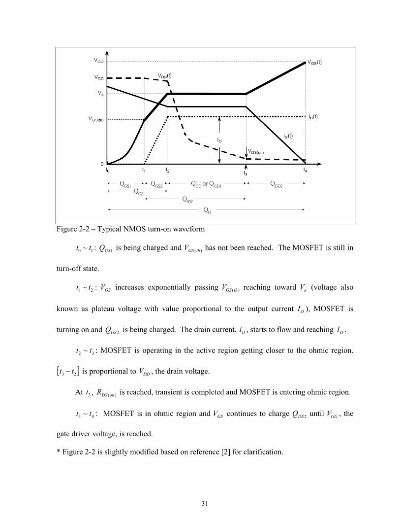
The general NMOS model is shown in Figure 2-1 with the characteristic capacitances
extracted from the MOSFET structure and parasitic inductances extracted from the MOSFET
package. The definition of capacitance commonly specified in the datasheet., issC , ossC and
rssC , are shown. Figure 2-2 shows the typical )(tVGS , )(tiG , )(tVDS and )(tiD waveforms of
the n-channel MOSFET during turn-on [4]*. This transient period is divided into 4 sections.
Figure 2-1 – General N-channel-MOSFET model
In Figure 2-2, 21 GSGSGS QQQ += is the total gate-to-source charge, 21 GDGDGD QQQ += is
the total gate-to-drain charge, which is commonly approximated by 1GDGD QQ ≅ . The total
gate charge, GDGSG QQQ += , is charges required to turn on a N-channel MOSFET. The total
charge is often broken into sub-charges verses time to better correspond them to the voltage
and current transient waveforms during MOSFET turn-on as shown in Figure 2-2. These sub-
charges are usually defined individually in MOSFET supplier’s datasheet in order to
characterize GDGSGDGSGDGSSW QQQQQQQ +≈+≈+= 2/212 more accurately. SWQ ,
commonly known as the switch charge, directly determines to the upper MOSFET switching
loss which is the most significant power loss in synchronous buck SMPS today.
Page 42
31
Figure 2-2 – Typical NMOS turn-on waveform
10 ~ tt : 1GSQ is being charged and )(thGSV has not been reached. The MOSFET is still in
turn-off state.
21 ~ tt : GSV increases exponentially passing )(thGSV reaching toward aV (voltage also
known as plateau voltage with value proportional to the output current OI ), MOSFET is
turning on and 2GSQ is being charged. The drain current, Di , starts to flow and reaching OI .
32 ~ tt : MOSFET is operating in the active region getting closer to the ohmic region.
[ ]23 tt − is proportional to DDV , the drain voltage.
At 3t , )(onDSR is reached, transient is completed and MOSFET is entering ohmic region.
43 ~ tt : MOSFET is in ohmic region and GSV continues to charge 2DSQ until GGV , the
gate driver voltage, is reached.
* Figure 2-2 is slightly modified based on reference [2] for clarification.
QGS1
QGS2
QGD
or QGD1
QSW
QGS
QG
QGD2
Page 43
32
High-Side NMOS (QH)
Referring back to Figures 1-9 and 1-11, during the dead-time before high-side is tuned on,
the drain-source voltage of the high-side NMOS is )( )(_ QLDiodeFDINnodephaseINds VVVVV −−=−=
INV> , so the drain-source capacitance, dsC , has been fully charged before switching starts.
Referring to Figure 2-2, the gate-source capacitance or charge, gsC or GSQ , , is fully charged
by 2t . Between 2t and 4t , the gate-drain capacitance, gdC is still been charged, but as shown
in Figure 2-3, the gate current charging the gate-drain capacitance is irrelevant to a model
which represent the load path. At 3t , the transient is completed and the high-side NMOS is
completely turned on where the ohmic region is reached. Therefore, the model for NMOS at
3t is simply package inductance in series with minimum on-resistance.
Figure 2-3 – High-Side NMOS equivalent model during turn-on
Page 44
33
Low-Side NMOS (QL)
The output or load current flows through the parasitic diode of the low-side NMOS during
the dead-time. During the high-side NMOS turn-on, the gate-source capacitance, gsC , is not
being charged because both the gate and source voltage are grounded. Before 1t , the high
gate driver is bringing phase-node potential from QLdiodeFDV )(− to 0V as shown in Figures 1-9
and 1-11. Between 1t and 3t , votlage at phase-node is rised from 0V to OUTQHonDSDD IRV )(− ,
the gate-drain, gdC , and gate-source, gsC , capacitances, i.e., gsgdoss CCC += , are being
charged while the parasitic diode of lower NMOS is also being recovered. The diode
recovery current waveform is shown in Figure 2-4. The effect of the diode recovery is
ignored for the equivalent model representing low-side NMOS during switching; this
approximation is acceptable for designing snubber circuit. Figure 2-5 shows the
approximated equivalent circuit of low-side NMOS during high-side NMOS turn-on.
Figure 2-4 – NMOS diode recovery waveform
Figure 2-5 – Low-Side NMOS equivalent model during High-Side NMOS turn-on
Figure 2-4 Figure 2-5
Page 45
34
2.2 Second-Order Equivalent Circuit of Load Path
Combining the above approximations, Figure 2-6 represents the load path of the NMOS
synchronous buck SMPS and its resonance condition during high-side NMOS turning on. It
is intuitively simplified in Figure 2-7 which is a second-order series RLC resonance circuit
with the natural and damping frequencies defined as:
LCn1
=ω (2-1)
21 Pnd ζωω −⋅= (2-2)
where the damping coefficient due to parasitic is LCR
P 2=ζ (2-3)
Figure 2-6 – Equivalent circuit representing the resonance condition during switching
Figure 2-7 – Simplified second-order circuit representing the resonance condition during
switching
Figure 2-6
R
L
C
Vin
t = 0
Figure 2-7
Page 46
35
Here, the board resistance and inductance are assumed negligible compared to MOSFET
)(onDSR and package lead inductance, this is a valid assumption with careful power circuit
PCB layout:
QLsQLdQHsQHd LLLLL ,,,, +++= (2-4)
QHonDSRR min,_)(= (2-5)
QLOSSCC ,= (2-6)
In most recent SMPS application, )(onDSR is typically in few hundred of mΩ range
maximum and C is typically smaller or in the same magnitude as L ; therefore, 12 <<Pζ .
Thus Equation (2-2) can be simplified as followed:
LCnd1
=≅ ωω (2-7)
The above second-order approximation of the load path (Figure 2-6 and 2-7) is what is
assumed in the literature surveys.
2.3 Determining RLC Values of Second-Order Equivalent
The load path of SMPS is assumed linear and approximated by second-order series RLC
as shown in Figure 2-7. The oscillation frequency at the phase-node is due to the parasitics of
the load path L and C , where R introduces amplitude damping. To design snubber element
analytically, the value of R , L , and C must be approximated first. Three methods are
presented below: obtaining from supplier, curve fitting from simulated waveforms with
MOSFET spice model, and curve fitting from measurements
Page 47
36
Obtaining from Supplier
The straight forward approach is to obtain these RLC parameters from the supplier. C
should be given in the datasheet, but the total parasitic L is usually not. L should roughly be
the same for the same MOSFET package from the same MOSFET supplier. It should be
noted that the value of L greatly depends on the number of bounding wires in the package; if
the bounding structure changes, L could change significantly. To obtain C values from the
datasheet, using Infineon MOSFET BSO119N03S as an example for 12V QHGSV , and inV , as
shown in Figure 2-8 below extracted from datasheet [3], Ω≅ mR onDS 9.11)( and
pFCC OSS 500≅= . Package stray parasitic L is not shown in datasheet which need to be
obtained from curve fitting methods.
Figure 2-8 – Infineon BSO119N03S MOSFET datasheet figures
Page 48
37
Curve Fitting from Simulated Waveform with MOSFET Spice Model
An alternate method is to simulate with MOSFET spice model from the supplier. Using
the spice BSO119N03S level-1 MOSFET model provided by Infineon, the simplified
synchronous buck SMPS simulated model is shown in Figure 2-9. The gate drivers are
modeled from measurements of RichTek RT9232 PWM controller [4] during high-side turn-
on transient with simulated 24V high-side gate driver. More accurate gate driver models can
be used involving closed loop feedback with floating boost-strap circuitry commonly found in
VM-controlled PWM controller. Although the circuit has all ideal passive components except
MOSFET spice models, for the purpose of obtaining RLC values of the load path, simple
circuit approximation as shown in Figure 2-9 is found to be sufficiently accurate. Figures 2-
10 and 2-11 show that the simulated and the measured waveforms are closely correlated.
Figure 2-9 – Synchronous buck SMPS simulation with supplier-provided Level-1 MOSFET
model
V
I
INDUCTOR
12V_BUS2012Vdc
I206Adc
LGATE20
TD = 50n
TF = 30nPW = 355nPER = 3000n
V1 = 12
TR = 25n
V2 = 0
UGATE35
TD = 80ns
TF = 37nsPW = 300nPER = 3000n
V1 = 0
TR = 8.8ns
V2 = 24
00
0
0
1 2L137 2.2uH
IC = 6A
Q139
BSO119N03S_L1
Q140
BSO119N03S_L1
LOAD
C436470uF
C435470uF
HIGH-SIDEMOSFET
BULK CAPS CERAMIC CAPS
LOW-SIDEMOSFET
C43820uF
C43710uF
HIGH-SIDEGATE DRIVER
LOW-SIDEGATE DRIVER
Page 49
38
Figure 2-10 – Simulated SMPS phase-node oscillation with Level-1 MOSFET model
Figure 2-11 – Measured SMPS phase-node oscillation
From the simulated oscillation frequency of 137MHz as shown in Figure 2-10, L can be
approximated from Equation (2-7) to be 2.7nH. With the capacitor value, pFCC OSS 500≅= ,
obtained from the MOSFET datasheet and nHLL totalstray 7.2_ ≈= , the simplified LC
oscillatory circuit without damping component is obtained as shown in Figure 2-12 and the
oscillation frequency (red trace of Figure 2-12) closely fits the simulated waveform with
spice-MOSFET model (green trace of Figure 2-12, phase-node from Figure 2-9 circuit).
Figure 2-12 – Simplified second-order LC circuit
Figure 2-10 Figure 2-11
Page 50
39
Correlation in Figure 2-12 shows that simple LC second-order equivalent circuit is
sufficiently accurate to model the load-path of the synchronous buck SMPS when high-side
NMOS is turning on; nevertheless, this equivalent circuit cannot represent the synchronous
buck SMPS load-path if additional elements, such as snubbers, are added to the circuit. In
Todd’s paper as shown in Figure 1-14, snubbers are connected in parallel with the capacitor at
node A of Figure 2-12. It is intuitive that the node A is not an accurate representation of the
phase-node of the SMPS load path simply because the stray inductance should be equally
distributed across the two NMOS as shown in Figure 2-6. Before a model that is more closely
representing the actual load path is developed, another method of approximating LC values
can be obtained from measurements if the MOSFET spice model is not available.
Curve Fitting from Measured Waveform
In the case when spice circuit cannot be easily constructed due to lack of models, the
oscillation frequency can be measured accurately from the oscilloscope and, similar to the
simulated approach, using the typical OSSC value obtained from MOSFET datasheet, the total
stray inductance can be approximated.
The actual circuit implementation of the synchronous buck SMPS used through out the
snubber design is presented here. The schematic and PCB layout of the design with RichTek
RT9232 PWM controller and Infineon BSO119N03S NMOS are shown in Figures 2-13 and
2-14. The schematic of PWM controller section is omitted as it is irrelevant, only the two
MOSFET driver pins are shown. The measured oscillation was previously shown in Figure 2-
Page 51
40
11 which correlates with simulated model of Figure 2-10. This results the same L
approximation of 2.7nH.
Figure 2-13 – Schematic of the SMPS implementation
Figure 2-14 – PCB layout of the SMPS load path snapshoot
Page 52
41
2.4 Second-Order Load Path Equivalent
The simple LC model of Figure 2-12 is modified to equally distribute the stray inductance
as shown in Figure 2-15, the voltage and current sources in the equivalent circuit are needed
to properly model current and voltage initial states of the current flowing through the low-side
NMOS diode during dead-time.
Damping resistances, PR , with arbitrary values are added in the model of Figure 2-15 in
order to obtain damping characteristic closely fitting the waveform to the MOSFET model.
As the turn-on transient is completed by 3t , the minimum on-resistance of the high-side
NMOS is reached and it is not sufficiently large enough to explain the damping as shown in
the MOSFET model. A more complete model would have to include the effects due to the
diode recovery and the parasitic bipolar transistor of the low-side NMOS under a sudden
increase of voltage at the phase-node. This requires complex non-linear MOSFET modeling
which is shown unnecessary and redundant for the purpose of snubber design. The model
presented in Figure 2-15 is sufficient to capture the transient behavior and it is also simple
enough to use Root-Loci method to design snubbers.
Figure 2-15 – Equivalent second-order RLC circuit representing SMPS load path
Page 53
42
Figure 2-16 shows simulated waveforms of voltage and current during switching. The red
simulated phase-node voltage from second-order approximation (circuit of Figure 2-15) is
closely fitting the green voltage waveform simulated with level-1 MOSFET model (circuit of
Figure 2-9). The current waveforms of both MOSFET and second-order models are also
shown to be closely correlated.
Figure 2-16 – Simulated phase-node oscillation and input current of Level-1 MOSFET model
and second-order model
This oscillation frequency and its peaks are the target noise source which the snubber
circuit is designed for; however, as snubber elements are attached at the phase-node, the load
path including the snubber elements can not be accurately modeled as a second-order
approximation. The following chapter demonstrates the method commonly adapted in
classical snubber design where the method assumes that the second-order approximation still
holds with snubber elements added to the circuit.
Page 54
43
3 SECOND-ORDER SNUBBER RESISTOR DESIGN
Figure 3-1 shows the approach that many sources demonstrated for snubber design based
on second order LC tank circuit approximation with added snubber resistor SR across the
parasitic capacitor [5]. The output/input transfer function has the form of a second order
response:
Figure 3-1 – Second-order approach of snubber resistor
( ) 22
2
2 211
1
11
11
)(nnS
n
SSS
SS
ssLCCR
ss
LC
sLsC
RsC
R
sCR
sCR
sHωωζ
ω++
=
+
+
=+
+
⋅
+
⋅
= (3-1)
The suggested approach uses the oscillatory frequency measured before the snubber
resistor is added; 137MHz in our example. The snubber resistance is then solved by selecting
the desired damping coefficient due to snubber resistor Sζ . Typical 5.0=Sζ is used to
obtain a balance between an acceptable damped oscillation and optimum resistive power
dissipation.
CL
CR
SnSS ζωζ 2
12
1== (3-2)
L
CVINR
sV
OUT
Page 55
44
It is simulated and experimented that the above second-order oscillatory circuit is highly
inaccurate to apply in snubber design. The value of the snubber resistor calculated is much
higher which the waveform with added snubber resistor added does not correspond to the
damping coefficient it should represent. Furthermore, the waveform shows a damped
frequency of 146MHz, which contradicts Equation (2-7) where the damped frequency should
not exceed the natural frequency of 137MHz for a second-order oscillatory circuit.
Table 3-1 – Snubber Resistor Calculation for 2nd-order Approximation
Figure 3-2 – Simulated waveform with snubber resistor of 2.32R based on 2nd-order
approximation.
(The amount of damping does not correspond to the damping coefficient of 0.5)
The second-order assumption calculates the snubber resistor added in parallel with the
parasitic capacitor alone; however, in synchronous buck SMPS application as shown in
Figure 3-3, the lower MOSFET stray inductor is in series with the capacitor parallel to the
snubber resistor.
Snubber Resistor for 2nd-order Approximation
InputOutput
Parameters Values Unit Comments
LS C_oss 5.00E-10 Ff_resonant 1.37E+08 Hz Simulated/MeasuredL_stray 2.70E-09 H f = 1/(2*pi*sqrt(L*C))R_snubber 2.32E+00 Ohms zeta set to 0.5 Table 3-1
Figure 3-2
Page 56
45
Figure 3-3 – Simplified equivalent SMPS load path with snubber resistor
Simulated waveforms of simple RLC oscillatory circuits in Figures 3-4 and 3-5 show that
while the calculated snubber resistor from Equation (3-2) yield good results in second-order
circuit Figure 3-4, it does not yield expected damping in a third-order approximation Figure
3-5 which represents the SMPS application. Both approximations without the snubber
resistor resonances at 137MHz as before, the damped waveform of the second-order circuit
corresponds to a damping coefficient of 0.5 with an expected lower damped frequency of
119MHz while the damped waveform of the third-order circuit still rings with higher damped
frequency of 139MHz. This further demonstrates that second-order calculation at best gives
only a preliminary initial snubber resistor which needs further tweaking.
CP
LP=L
stray/2
RS
VIN
VOUT
LLS
= L
D,LS +
L
S,LS
CP
LHS = LD,HS + LS,HS
VIN
VOUT
LP=L
stray/2
Page 57
46
Figure 3-4 – Second-order RLC oscillatory circuit with and without snubber resistor
Figure 3-5 – Third-order RLC oscillatory circuit with and without snubber
Page 58
47
4 HIGHER-ORDER SNUBBER DESIGN USING ROOT-LOCI
4.1 Snubber Resistor Design Criteria
The output/input transfer function based on Figure 3-3 with the snubber resistor SR ,
discarding the parasitic PR , is a third-order circuit where the snubber resistor SR does not
follow Equation (3-2) of the second-order assumption. The output/input transfer function of
Figure 3-3 is:
PP
S
PPP
S
PP
S
P
S
PPS
PPS
PPS
PPS
R
CLRs
CLs
LRs
CLRs
LR
sLsCsL
RsCsL
R
sCsLR
sCsLR
sH2
23
22
1211
11
)(+++
+=
+
+
++
⋅
+
++
⋅= (4-1)
The characteristic equation of the above third order transfer function is:
0122
23 =+++PP
S
PPP
S
CLRs
CLs
LRs (4-2)
Since the value, or the sensitivity of the change of the value, of SR to the overall system is
our interest, the characteristic equation above can be rearrange by dividing both sides of the
equations by the terms that do not contain SR as shown below.
01
2
13
22
=+
++
sCL
s
CLRs
LR
PP
PP
S
P
S
or 01
12
13
22
=+
+
+s
CLs
CLs
LR
PP
PPPS
, which is expressed as
0)(
)(1 =+sP
sQRS (4-3)
Page 59
48
Where PPP CL
sL
sQ 22 12)( += and s
CLssP
PP
1)( 3 +=
Equation (4-3) is a general Root-Locus problem. With known approximated values of PL
and PC obtained from curve-fitting in earlier section, the root-loci plot is shown in Figure 4-1.
The Root-Loci plot shows three branches for third-order system. The branches in green
and red are more dominant for the larger value of Rsnubber, but the effect of the real root
cannot be ignored completely because it is not at least 5 to 10 times further than the dominant
complex conjugate roots.
Figure 4-1 – Root-Loci of third-order approximation with changing snubber resistor
Before the optimum value of the snubber resistor is discussed, some correlations between
the Root-Loci plot and time-domain waveform are shown. The Root-Loci plot of Equation
(4-1) with R=0.85Ω is shown in Figure 4-2 where it indicates that the oscillation frequency
with added snubber resistor is 169MHz. Figure 4-3 is the Spice-MOSFET-model circuit with
Rss = [0:0.01:3,100]; L = 2.70E-9; Cp = 5E-10; Lp = L/2; Q = [2/Lp 0 1/(Lp*Lp*Cp)]; P = [1 0 1/(Lp*Cp) 0]; H = tf(Q,P) rlocus(H,Rss)
Page 60
49
added snubber resistor and Figure 4-4 is the third-order approximation with added snubber
resistor. The simulated results of these circuits are shown in Figure 4-5 where the green
waveform corresponds to circuit Figure 4-3 and the red waveform corresponds to circuit
Figure 4-4. It can be seen that the oscillation frequency of 169MHz found in Root-Loci plot
in Figure 4-2 corresponds to both green and red simulated waveform in Figure 4-5; and the
green waveform correspond visually to a damping coefficient of 0.203 as predicted in the
complex roots.
Figure 4-2 – Root-Loci of third-order approximation with changing Rsnubber
Figure 4-3 – MOSFET-model Spice schematic with snubber resistor
Rs = 0.85; q2 = Rs/Lp; q1 = 0; q0 = Rs/(Lp*Lp*Cp); p3 = 1; p2 = 2*Rs/Lp; p1 = (Lp*Cp)^-1; p0 = Rs/(Lp*Lp*Cp); q = [q2 q1 q0]; p = [p3 p2 p1 p0]; h = tf(q,p) rlocus(h) Transfer function: 6.296e008 s^2 + 9.328e026 --------------------------------------------- s^3 + 1.259e009 s^2 + 1.481e018 s + 9.328e026 f = 1.06e9/(2*pi) f = 1.6870e+008
Page 61
50
Figure 4-4 – Third-order Spice schematic with snubber resistor
Figure 4-5 – MOSFET-model and 3rd-order simulation with snubber resistor correlated with
Root-Loci plot
For optimal transient waveform, the voltage overshoot due to a step input should be low.
Referring to Figure 4-6 showing step-response comparison for various characteristic-
equation-root-locations in the s-plane [11], the first forth responses can help explaining the
contribution of each branch of the Root-Loci plot of Figure 4-1.
Page 62
51
Figure 4-6 – Step-response comparison for various characteristic-equation-root locations in
the s-plane
Page 63
52
The optimum value of Rsnubber is determined to be in the range of 0.5~0.85Ω because
the complex root pair is farthest away from the imaginary axis while the real root is not
relatively too far away from the imaginary axis as well. For the complex roots alone,
assuming the real root is far enough to be ignored, 0.85Ω is optimum value which gives the
lowest first overshoot amplitude underdamped waveform with shortest settling time because it
is farthest away from the imaginary axis (comparing 3rd and 4th responses in Figure 4-6).
However, the effect of real root become more significant when the resistor value is slightly
smaller then 0.85Ω; moving from 0.85Ω down to 0.5Ω, even though the complex roots
increase the amplitude and settling time, which appears to be less desirable, the real root also
moves toward the imaginary axis with a more-overdamped exponential waveform (comparing
1st and 2nd responses in Figure 4-6). The complex pair creates a decaying oscillating sine
waveform that rides on top of the exponential one. If the slow wave is damped sufficiently,
the sum of the two waveforms will have a lower first peak. The overall result would be a
preferred trade-off when these waveforms are superimposed; it has optimum oscillatory
transient waveform with lowest first overshoot amplitude.
As shown in Figure 4-7, simulated result of Figure 4-3 sweeping Rsnubber. Rsnubber
values between 0.4Ω and 0.85Ω yields quite desirable waveforms. As Rsnubber gets too
small, as predicted in Root-Loci, the real root becomes dominant and the waveform becomes
completely overdamped; this is undesirable because it creates loss in SMPS efficiency
without any benefit.
Page 64
53
Figure 4-7 – MOSFET-model simulation sweeping Rsnubber correlated with Root-Loci
predicted optimum value
Page 65
54
4.2 Snubber Capacitor Design Criteria
After an optimum Rsnubber is chosen, the Csnubber is added in series with Rsnubber in
the circuit as shown in Figure 4-8 (MOSFET-model) and Figure 4-9 (forth-order
approximated model). The optimum snubber resistor is chosen to be 0.7Ω based on previous
analyses. The role of the series snubber capacitor is critical for this application in order to
release thermal stress from the resistor and improve overall efficiency of SMPS. In our
example, if no snubber capacitor is used, 12V 10%-duty-cycle switching pulses at the phase-
node would put the 0.7Ω snubber resistor at 20W stress; the resistor will burn. Circuit
analysis of the snubber capacitor criteria and impacts is shown in Chapter 5.
Figure 4-8 – MOSFET-model Spice schematic with snubber resistor and capacitor
Figure 4-9 – 4th-order Spice schematic with snubber resistor and capacitor
Page 66
55
A new Root-Loci plot is created in Figure 4-10 based on the new system transfer function
shown below varying the Csnubber value this time with Rsnubber fixed at 0.7Ω. It shows that
with added snubber capacitor, the system is now a forth-order equivalent circuit.
+
+++
+++
++
+
+
+
=
222
234
2223
11122
11
)(
PSPP
P
S
P
P
S
PPPP
SP
SPP
P
P
S
PSPPP
S
PSP
S
RS
LCCs
CR
CR
CR
Ls
LCLRR
CLs
LR
LRs
LCCs
LCRs
LCs
LR
sH (4-4)
The characteristic equation:
+
+++
+++
++ 22
22
34 11122
PSPP
P
S
P
P
S
PPPP
SP
SPP
P
P
S
LCCs
CR
CR
CR
Ls
LCLRR
CLs
LR
LRs (4-5)
Dividing both sides of the equation by the terms that do not contain SC yields.
0112
121
1
22
234
222
=
+
++
++
+
+
+s
CR
CR
Ls
LCLRRs
LR
LRs
LCs
LRs
LC
P
P
P
S
PPPP
SP
P
P
P
S
PPP
P
PS (4-6)
Figure 4-10 – Root-Loci of forth-order approximation with changing Csnubber with fixed
0.7Ω Rsnubber
Xss = [5000000:100000:10000000000]; L = 2.70E-9; Cp = 5E-10; Lp = L/2; Rs = 0.7; Rp = 0.0119; p4 = 1; p3 = (2*Rs/Lp+Rp/Lp); p2 = (Rs*Rp/(Lp*Lp)+1/(Lp*Cp)); p1 = 1/(Lp*Lp)*(Rs/Cp+Rp/Cp); p0 = 0; q2 = 2/Lp; q1 = Rp/(Lp*Lp); q0 = 1/(Lp*Lp*Cp); q = [q2 q1 q0]; p = [p4 p3 p2 p1 p0]; h = tf(q,p) rlocus(h, Xss)
Page 67
56
The transient waveform of the system with RC snubber is now a forth order system. At a
small Csnubber value, there are two complex conjugate pairs. One pair (blue and green) has
higher frequency than the other (light blue and red). As Csnubber value increases, one
complex pair with lower frequency becomes real.
For optimum waveform of low first overshoot with a step input, superposition of
overshoots created by two pairs of complex roots should be avoided. This could be achieved
by setting the slow pair of roots to real (the only pair that can be made real), thus the
contribution of these roots now creates overdamped exponential waveform instead of
underdamp (comparing 2nd and 3rd responses in Figure 4-6). When Csnubber is 10nF (Gain =
1/Cs = 1e8) shown in Figure 4-10, this is the critical and minimum snubber capacitor value
that puts the slow pair on real axis; the slow pair is now critically damped while the fast pair
determines the overshoot. Increasing the capacitor value moves one of the real roots closer to
the imaginary axis and creates an overdamped (1st response in Figure 4-6) while the complex
roots creates higher overshoots (comparing 3rd and 4th responses in Figure 4-6). Overall, this
is the range of the snubber capacitor value that gives an optimum waveform. Similar to the
previous analysis on Rsnubber, Csnubber value is picked optimally so that the two real roots
are larger than the value that gives critically damped to create a more-overdamped
exponential waveform.
The Root-Loci plot with changing Csnubber at fixed 0.7Ω Rsnubber is shown in more
details in Figure 4-11 to compare to measurements and simulation captures shown in Figures
4-12, 4-13 and 4-14, where Csnubber varying from 2.2nF to 10nF to 22nF respectively with a
Page 68
57
fixed Rsnubber of 0.7Ω. For Figures 4-12, 4-13 and 4-14, measured waveforms are on the
left-hand side and simulated waveforms are on the right-hand side where green traces are
from Spice-MOSFET-model of Figure 4-8 and red traces are from 4th-order approximation of
Figure 4-9. As shown in Figure 4-13, Csnubber is 10nF, the waveform correlates to the
slower-frequency complex root branch turning to real root in Root-Loci on Figure 4-11; both
measurements and simulations show a high first overshoot about 6V overshoot on 12V rail,
which is about 50% as predicted in Root-Loci plot (51.6%). Around 160MHz is measured
correlated with around 180MHz simulated and predicted in Root-Loci (1.12e9 rad/s) plot.
Figure 4-11 – Root-Loci of forth-order approximation with changing Csnubber with fixed
0.7Ω Rsnubber (details)
Page 69
58
Figure 4-12 shows Csnubber at 2.2nF, smaller than the critical value of 10nF, which Root-
Loci has four complex roots, it can be observed in both measurements and simulations that
the fast frequency (180MHz measured correlated with Root-Loci 200MHz or 1.27e9 rad/s)
superimposed on a slower frequency (60MHz measured and 80MHz or 5.58e8 rad/s Root-
Loci, simulations are off most likely due to aliasing of two frequencies). The overshoot
increases to 8V (67%) as expected where this value cannot be easily observed from Root-Loci
due to 2 sets of complex roots.
Figure 4-14 shows the optimum snubber capacitor value of roughly 22nF. The frequency
is around 160MHz measured and 180MHz simulated and predicted in Root-Loci (1.12e9
rad/s). The overshoot decreases to 4V (33%) and the overshoot value cannot be predicted
from the complex roots of Root-Loci plot because the real roots (overdamped waveform) is
now dominant over the complex roots. Overall, these measurements and simulations very
closely correlate with what is predicted in Root-Loci plot.
Increasing Csnubber further would make the real root more dominant, turn the overall
waveform to be overdamped, as Figures 4-12, 4-13 and 4-14 show, and reduce overall SMPS
efficiency. In addition, higher snubber capacitor will also put more stress on the snubber
resistor power dissipation during switching with little or no benefit. This is significant for
choosing resistor footprint size.
Page 70
59
Figure 4-12 – Measurement vs. MOSFET and forth-order simulation – 0.7Ω + 2.2nF
Figure 4-13 – Measurement vs. MOSFET and forth-order simulation – 0.7Ω + 10nF
Figure 4-14 – Measurement vs. MOSFET and forth-order simulation – 0.7Ω + 22nF
Page 71
60
4.3 Final Snubber RC Value Verification
The snubber R and C are optimally determined individually as shown previously. Re-
arranging the Characteristic Equation (4-5) of the forth-order circuit slightly by dividing both
sides of the equation by the terms that do not contain SR this time with SC fixed at 22nF, the
Root-Loci plot is shown in Figure 4-15.
Figure 4-15 – Root-Loci of 4th-order approximation with changing Rsnubber with fixed 22nF
Csnubber
As it is shown, our chosen R value (Gain) maintained to be an optimum value in series
with snubber C. This is a verification to ensure that by introducing snubber C does not affect
the optimum snubber R. The optimum values are acceptable and reccursive design is not
required.
Page 72
61
4.4 Snubber Design without Snubber Resistor
This is to investigate the effect of the Csnubber without Rsnubber which is a
simplification used in some practical designs. Figure 4-16 shows the equivalent circuit of
adding Csnubber without Rsnubber. The figure on the left is an ideal scenario which is not
realizable, whereas the figure on the left represents the real capacitor with parasitic series ESR.
This section is to show that ideally with only capacitor alone, the circuit is proved to be
undamped based on Root-Loci. However, in practice, due to the parasitic ESR of the
capacitor, some damping will be observed. It will be shown that the waveform would still be
undesirable unless the ESR is large enough to be close to the optimum snubber resistor value
required.
Figure 4-16 – Ideal and real equivalent circuit representation of SMPS load path with
Csnubber alone
CP
LP
CS
VIN
VOUT
LP
CP
LP
CS
VIN
VOUT
LP
CS_ESR
Page 73
62
The transfer function with the snubber capacitor along is:
+
++
+
+
=
223
22
11111
11
)(
PSPSPPSP
PSPPSCS
LCCs
CCLs
CLs
LCCs
LCsH (4-7)
The characteristic equation:
0111112
23 =
+
++
+
PSPSPPSP LCCs
CCLs
CLs (4-8)
Dividing both sides of the characteristic equation by the terms that do not contain SC yield
01
1111
13
22
=
+
+
+
+s
LCs
LCs
Ls
LC
PP
PPPPS (4-9)
The Root-Loci plot is shown in Figure 4-17 where there are two identical pure complex
roots and zeros. Referring to the forth response of Figure 4-6, this shows that any value of
Csnubber will make the system undamped. Correlation of this prediction from Root-Loci is
shown with simulated waveforms with MOSFET model (Figure 4-18) and third-order
approximation (Figure 4-19).
Page 74
63
Figure 4-17 – Root-Loci of 3rd-order approximation with changing Csnubber without
Rsnubber
Figure 4-18 – MOSFET-model Spice schematic with snubber capacitor alone
Figure 4-19 – 3rd-order Spice schematic with snubber capacitor alone
Xss = [1000000:100000000:10000000000]; L = 2.70E-9; Lp = L/2; Cp = 5E-10; q2 = (1/Lp); q1 = (1/Lp); q0 = 1/(Lp*Lp*Cp); p3 = 1; p2 = 0; p1 = 1/(Lp*Cp); p0 = 0; q = [q2 q1 q0]; p = [p3 p2 p1 p0]; h = tf(q,p) rp = roots(p) rq = roots(q) rlocus(h, Xss) rp = 1.0e+009 * 0 0 + 1.2172i 0 - 1.2172i rq = 1.0e+009 * -0.0000 + 1.2172i -0.0000 - 1.2172i
Page 75
64
Unsurprisingly, the simulated waveforms shown in Figure 4-20 are almost undamped with
a Csnubber of 22nF, which was previously determined to be the optimum value.
Figure 4-20 – MOSFET and third-order simulation with snubber capacitor alone (unstable)
Obviously, an ideal Csnubber without any series parasitic resistance shown above is not
realizable. If a real capacitor is used, Root-Loci plot of Figure 4-15 can be borrowed to
explain the effect. It clearly shows in Root-Loci that small value of R would create high-
oscillatory waveforms unless the ESR of the capacitor happens to be close to the optimum
snubber resistor range.
Page 76
65
4.5 Optimum Snubber Resistor using Maxim’s Approach
Using the approach presented in Maxim’s Application Note 907 discussed in Literature
Surveys & Existing Methods of Snubber Designs section, it is suggested that the optimum
snubber resistor to damp the overshoot is twice the inductive impedance at the resonant
frequency with the added Csnubber alone. This approach is different from most of second-
order approximation, and it is therefore discuss here for comparison.
Taking the optimum snubber capacitor value of 22nF as previously determined, the Root-
Loci plot of the Csnubber alone shows a resonance frequency of roughly 26MHz. From
Equations (1-9) and (1-10):
Ω=≈= − 44.0)7.2)(26(22 96_ eeLfZ Csnubberwith ππ
Ω== 88.02 LZRsnubber
The snubber resistor value is actually predicted quite closely to Root-Loci result.
However, it is important to realize that the snubber capacitor value used in this calculation
was 22nF determined from Root-Loci result presented in this thesis to begin with. The
original Maxim’s recommendation of the snubber capacitor was to add capacitor to the circuit
until the original ringing frequency is cut in half. The original frequency was measured and
simulated to be 137MHz as shown in Figure 2-10 and 2-11, if the Maxim approach of
estimating the snubber capacitor were used instead of the method presented in this thesis, the
new frequency after the capacitor would have been 137MHz/2 = 68.5MHz; the optimum
snubber resistor would have then be calculated to be 2.32Ω instead.
Page 77
66
5 SNUBBER CAPACITOR BOUNDARY CRITERIA USING CIRCUIT
THEORY
Previous chapter uses Root-Loci approach to obtain snubber design criteria. The
minimum snubber capacitor value was chosen by moving a pair of complex roots on real axis
and the upper bound was determined from simulations or measurements. This chapter
investigates if snubber capacitor value boundaries can be determined using circuit approach.
5.1 The Upper Bound of Snubber Capacitor
The purpose of the snubber capacitor is to release thermal stress of the snubber resistor.
The smaller the capacitor value is, the faster it is charged and the lower the resistive power
loss is in the snubber resistor. From the circuit analysis, the upper bound of the snubber
capacitor value can be determined based on how much power the resistor is designed to
handle. As shown in Figure 5-1, the exponentially-charged voltage at the snubber capacitor
(VCsnubber) during switching reduces the voltage drop across the snubber resistor (Vphase-
VCsnubber). As soon as the capacitor is fully charged after transient turn-on or turn-off of the
upper MOSFET, the resistor is released from its thermal stress until the next switching occurs.
Simulation on Figure 5-1 with Csnubber value varying from 2.2nF to 50nF show the variation
of Vcsnubber waveforms (charging voltage at the snubber capacitor with respect to ground).
Looking at the Vphase-VCsnubber in the case of Csnubber = 50nF, power dissipated in the
snubber resistor is expected to increase with minimum benefit on the shape of the Vphase
waveform. On the other hand, 2.2nF has significant first overshoot because the capacitor is
Page 78
67
charged up too quickly compensating the benefit of snubber network. Both 10nF and 22nF
show adaquate waveform shape slightly lower first overshoot on 22nF at the cost of higher
thermal stress on the resistor. These correlates closely with Figures 4-12. 4-13 and 4-14.
Figure 5-1 – MOSFET model simulation showing VCsnubber waveform varying Csnubber
with 0.7Ω Rsnubber
To calculate for the upper bound of the snubber capacitor value based on the allowable
snubber resistor power requirement, we can determine for the maximum power dissipation of
the resistor for the entire switching period.
Page 79
68
Maximum Resistive Power Dissipation
From Figure 5-2, the maximum power dissipated in the resistor can be approximated.
This gives the worse-case wattage of the snubber resistor assuming step-response Vphase
voltage with 99% rise-time VCsnubber, based on %99)1( 5 ≈− −e . The upper limit of the
integral is 5 times the RC snubber time constant or RC5 , where R is the snubber resistor and
C is the snubber capacitor.
( ) ( )∫⋅≈
RC RsnubberSMPSMAXRsnubber dt
RtVfP
5
0
2
_)(2 (5-1)
( ) ( )∫
−⋅≈
RC CsnubberphaseSMPS dt
RtVV
f5
0
2max_ )(
2
( ) ∫
−−
⋅≈
−RCRCt
phasephaseSMPS dteVVR
f5
0
2
max_max_ 112
( ) ( )RC
RCt
phaseSMPS
RCRC
tphase
SMPS eRCR
Vfdte
RV
f5
0
22max_5
0
22max_
222
−
⋅=
⋅≈
−−
∫( ))5(22
max_ 1 −−⋅⋅⋅≈ eVfC phaseSMPS
( )2max__ phaseSMPSMAXRsnubber VfCP ⋅⋅≈ (5-2)
Figure 5-2 – Timing for calculating maximum Rsnubber power dissipation
Voltage
Time0
Vin - UVdsmin
~ = Vin
Vphase = LVds
VCsnubber = Vphase * [ 1 - exp( -t /RC)]
VRsnubber = |Vphase - VCsnubber|
Page 80
69
Equation (5-2) yields the same result as what is given in Todd’s paper, where the snubber
resistor is assumed to dissipate in worse case the charging and discharging of the total energy
stored in the snubber capacitor, SMPSMAXPhaseMAXRsnubber fVCP
⋅⋅= 2
__ 212 . Applying Equation
(5-2) to our example, kHzf SMPS 300= and VVphase 12max_ = with a standard-805-footprint
film resistor which has a rated power dissipation of WP MAXRsnubber 125.0_ = , the upper bound
of the snubber capacitor is only nFCsnubber 9.2max_ = .
With a 805-foorprint-resistor, the boundary of the maximum capacitor value is much
smaller than what we had calculated in Root-Loci. As shown in simulated and measured
waveforms in previous chapter, a snubber capacitor of 2.9nF would not have any
improvement to the switching waveform, this indicates that the size of the snubber resistor
should be increased to handle more power. The maximum power has linear relationship with
the capacitance; therefore, for an optimum 22nF we obtained from Root-Loci plot, the resistor
must be 1W-rated; this means significant PCB real-estate for typical micro-electronic circuit
today. For the above reasoning, 10nF snubber capacitor is the optimum value with significant
advantage in terms of power dissipation. The trade-off is obviously the waveform shape as
discussed in previous chapter but it is shown in Figures 4-13 and 4-14 that both 10nF and
22nF can provide adaquate damping.
Figure 5-3 (Circuit 1) shows the simplest circuit to evaluate the average power dissipated
in the resistor for a RC circuit with pulsating source. The results are shown in Table 5-1
which are within the maximum calculated values. Figure 5-3 (Circuit 2) shows the circuit
Page 81
70
which represents closer to the application of SMPS snubbers with Level-1 MOSFET models.
The average power dissipated in the snubber resistor with various snubber values are shown
in Table 5-1 to compare with the calculated values.
Figure 5-3 – Simulation of resistor power dissipation
Circuit 1 – RC with pulsating source
Circuit 2 – SMPS snubbers with Level-1 MOSFET model
Page 82
71
Table 5-1 compares the calculated snubber resistor power dissipation from Equation (5-2)
with the various simulated results of the simple RC circuit (Circuit 1) and the SMPS circuit
(Circuit 2) of Figure 5-3. As expected, all values simulated with Circuit 1 is within the
calculated boundary, comparing the case of 0.7Ω+10nF vs. 1.5Ω+10nF, the power in the 1.5Ω
resistor increases due to higher RMS voltage profile; but it is still bounded by the maximum
power based on conservation of energy in snubber capacitor. With Circuit 2, the average
power is close to estimated values which can be explained by the overshoots and ringing at
the phase-node and the ideal 12vdc source at the drain of the upper MOSFET. In real
implementation, as the block diagram shown in Figure 1-8 and the schematic shown in Figure
2-13, the input bead connected at the drain of the upper MOSFET would limit the transient
current can also reduce the dissipated power.
Table 5-1 – Calculated and simulated resistor power dissipation
Table 5-2 shows the results of measured temperatures of 805-footprint-0.125W-rated of
various snubber values. The temperature does not have insigificant dependancy to the
snubber resistor value the these ranges. 0.7Ω+10nF snubbers have a temperature of 63
degreeC which appears low for a calculated and simulated value of 0.43W. This can be
explained by the fact that the power rating of the resistor is determined based on the worse-
case thermal capability of the resistor without considering the actual layout. When the
Calculated from Equation (5-2)
Simulated results from Circuit 1 of Figure 5-3
Simulated results from Circuit 2 of Figure 5-3
Snubber Resistor Snubber Resistor Snubber ResistorSnubber Capacitor 0.7Ω
Snubber Capacitor 0.7Ω 1.5Ω
Snubber Capacitor 0.7Ω
10nF 0.43W 10nF 0.29W 0.36W 10nF 0.43W 22nF 0.95W 22nF 0.79W 0.88W 22nF 0.95W 47nF 2.03W 47nF 1.87W 1.95W 47nF 2W
Page 83
72
resistor is mounted on Printed Circuit Board (PCB) as shown in Figure 2-14, the copper island
of the phase-node serves as a local heatsink to the resistor.
Table 5-2 – Measured temperature of snubber resistor
Minimum Average Resistive Power Dissipation
For our application where the RC time constant, nseCR SSS 7107.0 9 ≈⋅== −τ , is in the
same order of the rise-time of the phase voltage, Todd’s paper suggestes that the minimum
power of the resistor would be SCSSCSSSMIN RVCfRVfCRQfRIP 222222 4)2()2( ==∆⋅==
based on the average current. WVnFKPMIN 02.0)7.0()12()22()300(4 222 <Ω= with our
values. The simulation results of Table 5-1 indicates that the minimum power dissipation
serves little to no usefulness because they are closer to the boundary of maximum power
dissipation.
Resistive One-Time Pulse Power Dissipation
Another approach to evaluate the allowable power dissipated in the resistor is to use one-
time pulse power characteristics. This is a specification of the resistor indicating the limit of
wattage which a particular type of resistor will not flame at the first application of power.
Although pulses are repeated in our application based on switching frequency and duty-cycle,
it must be assumed that each pulse is an one-time pulse when the period of its occurance is
much longer than the pulse width to use this approach.
Snubber Resistor Snubber Capacitor 0.7Ω 1.5Ω
10nF 63 degC n/a 22nF 75 degC 74 degC 47nF 123 degC n/a
Page 84
73
The peak power during switching is calculated as:
WVR
VP phase
peakRsnubber 2067.0
12 22
_ ≈Ω
== (5-3)
Figure 5-4 shown below [9] is a particular type of the resistor from a manufacturer used
here as an example. A 805-footprint resistor can sustain 200W of power under a sµ10 -width
pulse. In our application, the pulse is only few tens of nanoseconds, which is also a decaying
shape rather than a squared pulse; therefore, a 805-footprint resistor is acceptable using this
approximation.
Figure 5-4 – Resistor pulsed power characteristic
It would be more reasonable to apply one-time pulse power approximation when the
frequency is slow and the duty-cycle is around 50% where one-time pulse can be safetly
assumed. For our scenario, at 300kHz and 10% duty-cycle, the maximum power dissipation
based on Equation (5-2) gives more safe margin. A 1206-footprint-0.5W-rated resistor is
recommended.
Page 85
74
5.2 The Lower Bound of Snubber Capacitor
Referring to the literature surveys, if second-order assumption is applied with added
snubbers, the value of the capacitor is suggested between 2~9 times of the parasitic
capacitance of the original circuit. However, with Root-Loci method, snubber capacitor of
value nF10 is suggested as the minimum value (without considering practical limitation due
to power dissipation on the snubber resistor), which is already 20 times the parasitic
capacitance of pF500 . There is a minimum required RC time constant, which must be
greater than the rise-time of the voltage where the snubbers apply to. For a quick back-of-
envelop calculation, for a typical voltage rise-time of 10ns, if OhmRS 1= , then
nFC MINS 10_ = .
For our application, due to consideration of practical power limitation of the snubber
resistor, the selected optimum snubber capacitor is acutally at its minimum boundary.
Page 86
75
6 CONCLUSION
This thesis presents a new analytical approach for designing passive RC snubbers for
continuous-current voltage-mode synchronous buck SMPS. This approach uses Root-Loci
method when the overall circuit after adding snubber elements need to be represented with
higher than second-order equivalent circuit. It is demonstrated in this thesis that the method is
accurate, the design trade-offs are analytically intuitive and the results are easily obtained
with aid of commercial mathematical tools such as Matlab.
It is also proven in the thesis that exiting RC snubber design method, which based on the
assumption that the system with added snubbers can still be approximated accurately by
second-order equivalent circuit, does not provide expected outcome for this application. The
effect of RC snubbers with value obtained from this approximation contradicts the principle
of second-order equivalent circuit and the waveforms are not improved with these values.
The simulated and measured results using Root-Loci method presented correlate with
expected results with desirable waveform shapes. While the optimum snubber values are
suggested from Root-Loci plot, the minimum snubber values are bounded by the RC time
constant to the voltage rise-time, and the maximum snubber values are bounded by power
dissipation of the snubber elements.
Some improvements can be done to correlate MOSFET parasitics (the key parameter is
the lead inductance) with more samples or with different types of packaging technology.
Page 87
76
Board parasitics can also be included in the analysis as well as a non-ideal input voltage or
current source for the power supply. The design method can be verified with other power
supply topologies (boost, flyback, etc) or some investigations can be done to cover other
operational modes (e.g., discontinouse-current). EMI signatures with or without snubbers can
be studied to confirm if spikes and ringing of switching operation have significant compliance
impact. This research can also be further exteded for higher DC load current where more
complex linear models might be required to capture other MOSFET parameters such as
reverse recovery or intrinsic parasitic p-n-p transistor which are currently ignored in this
thesis. A more indepth study and comparison of different types of MOSFET technology (e.g.,
body diode vs. Schoktty diode) with several leading suppliers can also capture other
unforeseen dependancies and can help verify the robustness of this design method.
The approach presented in this thesis is currently being applied to switch mode power
supply designs in various consumer graphic board products at ATI Technologies Inc. The
design is proven with expected performance with optimum cost and good production yield.
Page 88
77
REFERENCES
[1] G. Nöbauer, D. Ahlers, and J. Sevillano-Ruiz, “A method to determine parasitic inductances in
buck converter topologies”, Infineon Technologies, June 2004
[2] K.S.Oh, “AN9010 - MOSFET Basics”, Fairchild Semiconductor, July 2000
[3] “Datasheet BSO119N03S”, Infineon Technologies, Oct. 2003
[4] “Datasheet RT9232 Programmable Frequency Synchronous Buck PWM Controller”, RichTek
Technologies, Nov. 2004
[5] Philip C. Todd, “Snubber Circuits: Theory, Design and Application”, May 1993
[6] Jim Hagerman, “Calculating Optimum Snubbers”, Hagerman Technology, Dec. 1994
[7] “AN848 - Snubber Circuits Suppress Voltage Transient Spikes in Multiple Output DC-DC
Flyback Converter Power Supplies”, Maxim Semiconductor, Nov. 2001
[8] “AN907 - R-C Snubbing for the Lab”, Maxim Semiconductor, Dec. 2001
[9] “Pulsed Power Characteristics” NIC Component Corp, Nov. 2002
[10] Benjamin C. Kuo and Farid Golnaraghi, “Automatic Control Systems – Eighth Edition”, Wiley,
2002
[11] William McMurray, “Optimum Snubbers for Power Semicondocturs”, IEEE IAS Transactions,
Vol. IA-8, No. 5, Sept/Oct 1972, pp. 593-600
[12] Bendien, Van Der Broeck and Fregien, “Recovery Circuit for Snubber Energy in Power
Electronic Application with High Switching Freuqencies”, IEEE Transactions on Power
Electronics, VOL. 3, NO. 1, January 1988, pp. 26-30
[13] Irving M. Gottlieb, “Power Supplies, Switching Regulators, Inverters, and Converters”, Second
Edition, McGraw Hill, 1994
[14] Marty Brown, “Practical Switching Power Supply Design”, Academic Press, 1990
[15] Marty Brown, “Power Supply Cookbook”, Butterworth-Heinemann, 1994
[16] John D. Lenk, “Simplified Design of Switching Power Supplies”, Butterworth-Heinemann, 1995
[17] Keith Billings, “Switchmode Power Supply Handbook”, McGraw-Hill, 1989
[18] George Chryssis, “High-Frequency Switching Power Supplies: Theory and Design”, Second
Edition, McGraw-Hill, 1989
[19] Abraham I. Pressman, “Switching Power Supply Design”, McGraw-Hill, 1991