• Continuous Short-Circuit Protection• Wide Common-Mode and Differential Voltage
Ranges• No Frequency Compensation Required• Low Power Consumption• No Latch-Up• Unity-Gain Bandwidth . . . 3 MHz Typ• Gain and Phase Match Between Amplifiers• Low Noise . . . 8 nV/√Hz Typ at 1 kHz
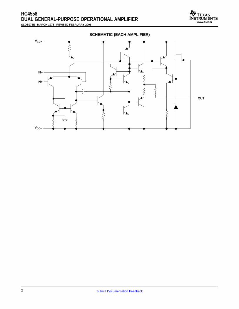
The RC4558 device is a dual general-purpose operational amplifier, with each half electrically similar to theµA741, except that offset null capability is not provided.
The high common-mode input voltage range and the absence of latch-up make this amplifier ideal forvoltage-follower applications. The device is short-circuit protected, and the internal frequency compensationensures stability without external components.
ORDERING INFORMATION
TA PACKAGE (1) ORDERABLE PART NUMBER TOP-SIDE MARKING
MSOP/VSSOP – DGK Reel of 2500 RC4558DGKR YR_ (2)
PDIP – P Tube of 50 RC4558P RC4558P
Tube of 75 RC4558DSOIC – D RC4558
0°C to 70°C Reel of 2500 RC4558DR
SOP – PS Reel of 2000 RC4558PSR R4558
Tube of 150 RC4558PWTSSOP – PW R4558
Reel of 2000 RC4558PWR
MSOP/VSSOP – DGK Reel of 2500 RC4558IDGKR YS_ (2)
PDIP – P Tube of 50 RC4558IP RC4558IP
Tube of 75 RC4558ID–40°C to 85°C SOIC – D R4558I
Reel of 2500 RC4558IDR
Tube of 150 RC4558IPWTSSOP – PW R4558I
Reel of 2000 RC4558IPWR
(1) Package drawings, standard packing quantities, thermal data, symbolization, and PCB design guidelines are available atwww.ti.com/sc/package.
(2) The actual top-side marking has one additional character that designates the assembly/test site.
Please be aware that an important notice concerning availability, standard warranty, and use in critical applications of TexasInstruments semiconductor products and disclaimers thereto appears at the end of this data sheet.
over operating free-air temperature range (unless otherwise noted)
MIN MAX UNIT
VCC+ 18Supply voltage (2) V
VCC– –18
VID Differential input voltage (3) ±30 V
VI Input voltage (any input) (2) (4) ±15 V
Duration of output short circuit to ground, one amplifier at a time (5) Unlimited
D package 97
DGK package 172
θJA Package thermal impedance (6) (7) P package 85 °C/W
PS package 95
PW package 149
TJ Operating virtual junction temperature 150 °C
Tstg Storage temperature range –65 150 °C
(1) Stresses beyond those listed under Absolute Maximum Ratings may cause permanent damage to the device. These are stress ratingsonly, and functional operation of the device at these or any other conditions beyond those indicated under Recommended OperatingConditions is not implied. Exposure to absolute-maximum-rated conditions for extended periods may affect device reliability.
(2) All voltage values, unless otherwise noted, are with respect to the midpoint between VCC+ and VCC–.(3) Differential voltages are at IN+ with respect to IN–.(4) The magnitude of the input voltage must never exceed the magnitude of the supply voltage or 15 V, whichever is less.(5) Temperature and/or supply voltages must be limited to ensure that the dissipation rating is not exceeded.(6) Maximum power dissipation is a function of TJ (max), θJA, and TA. The maximum allowable power dissipation at any allowable ambient
temperature is PD = (TJ (max) – TA)/θJA. Operating at the absolute maximum TJ of 150°C can affect reliability.(7) The package thermal impedance is calculated in accordance with JESD 51-7.
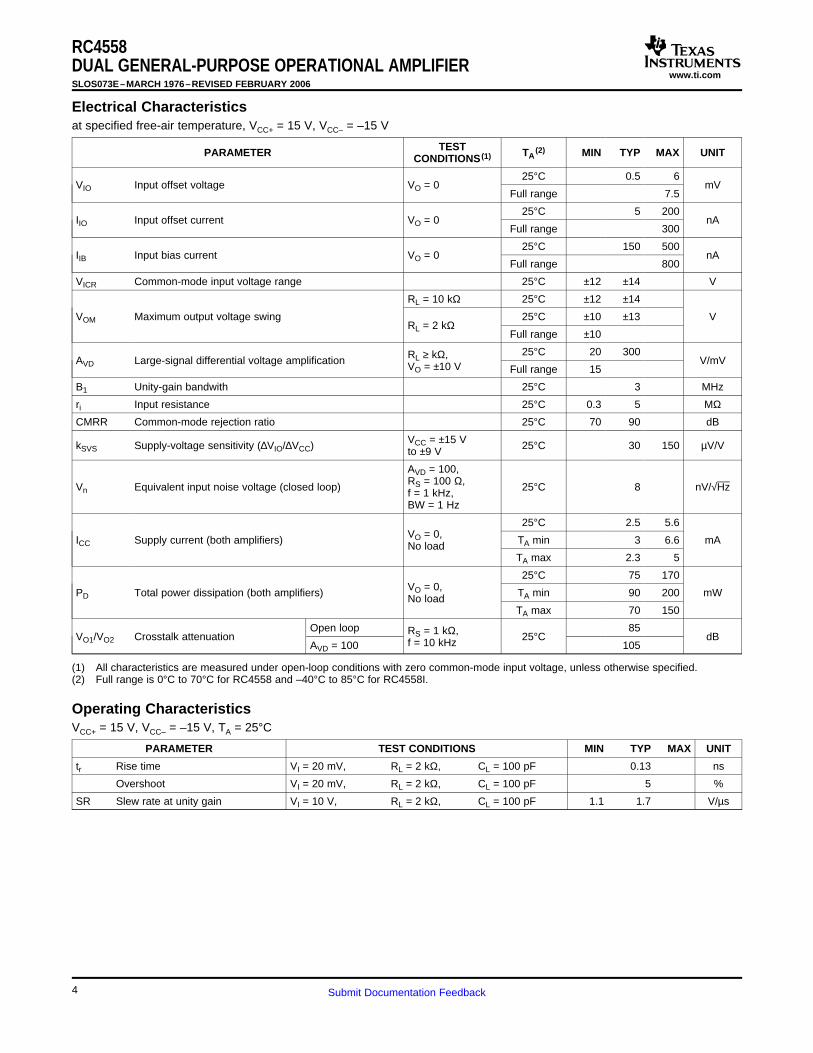
(1) All characteristics are measured under open-loop conditions with zero common-mode input voltage, unless otherwise specified.(2) Full range is 0°C to 70°C for RC4558 and –40°C to 85°C for RC4558I.
VCC+ = 15 V, VCC– = –15 V, TA = 25°C
PARAMETER TEST CONDITIONS MIN TYP MAX UNIT
tr Rise time VI = 20 mV, RL = 2 kΩ, CL = 100 pF 0.13 ns
Overshoot VI = 20 mV, RL = 2 kΩ, CL = 100 pF 5 %
SR Slew rate at unity gain VI = 10 V, RL = 2 kΩ, CL = 100 pF 1.1 1.7 V/µs
Orderable Device Status (1) Package Type PackageDrawing
Pins Package Qty Eco Plan (2) Lead/Ball Finish
MSL Peak Temp (3) Samples
(Requires Login)
RC4558PWRE4 ACTIVE TSSOP PW 8 2000 Green (RoHS& no Sb/Br)
CU NIPDAU Level-1-260C-UNLIM Contact TI Distributoror Sales Office
RC4558PWRG4 ACTIVE TSSOP PW 8 2000 Green (RoHS& no Sb/Br)
CU NIPDAU Level-1-260C-UNLIM Contact TI Distributoror Sales Office
RC4558Y OBSOLETE DIESALE Y 0 TBD Call TI Call TI Samples Not Available (1) The marketing status values are defined as follows:ACTIVE: Product device recommended for new designs.LIFEBUY: TI has announced that the device will be discontinued, and a lifetime-buy period is in effect.NRND: Not recommended for new designs. Device is in production to support existing customers, but TI does not recommend using this part in a new design.PREVIEW: Device has been announced but is not in production. Samples may or may not be available.OBSOLETE: TI has discontinued the production of the device.
(2) Eco Plan - The planned eco-friendly classification: Pb-Free (RoHS), Pb-Free (RoHS Exempt), or Green (RoHS & no Sb/Br) - please check http://www.ti.com/productcontent for the latest availabilityinformation and additional product content details.TBD: The Pb-Free/Green conversion plan has not been defined.Pb-Free (RoHS): TI's terms "Lead-Free" or "Pb-Free" mean semiconductor products that are compatible with the current RoHS requirements for all 6 substances, including the requirement thatlead not exceed 0.1% by weight in homogeneous materials. Where designed to be soldered at high temperatures, TI Pb-Free products are suitable for use in specified lead-free processes.Pb-Free (RoHS Exempt): This component has a RoHS exemption for either 1) lead-based flip-chip solder bumps used between the die and package, or 2) lead-based die adhesive used betweenthe die and leadframe. The component is otherwise considered Pb-Free (RoHS compatible) as defined above.Green (RoHS & no Sb/Br): TI defines "Green" to mean Pb-Free (RoHS compatible), and free of Bromine (Br) and Antimony (Sb) based flame retardants (Br or Sb do not exceed 0.1% by weightin homogeneous material)
(3) MSL, Peak Temp. -- The Moisture Sensitivity Level rating according to the JEDEC industry standard classifications, and peak solder temperature.
Important Information and Disclaimer:The information provided on this page represents TI's knowledge and belief as of the date that it is provided. TI bases its knowledge and belief on informationprovided by third parties, and makes no representation or warranty as to the accuracy of such information. Efforts are underway to better integrate information from third parties. TI has taken andcontinues to take reasonable steps to provide representative and accurate information but may not have conducted destructive testing or chemical analysis on incoming materials and chemicals.TI and TI suppliers consider certain information to be proprietary, and thus CAS numbers and other limited information may not be available for release.
In no event shall TI's liability arising out of such information exceed the total purchase price of the TI part(s) at issue in this document sold by TI to Customer on an annual basis.
NOTES: A. All linear dimensions are in millimeters.B. This drawing is subject to change without notice.C. Body dimensions do not include mold flash or protrusion not to exceed 0,15.D. Falls within JEDEC MO-153
IMPORTANT NOTICE
Texas Instruments Incorporated and its subsidiaries (TI) reserve the right to make corrections, modifications, enhancements, improvements,and other changes to its products and services at any time and to discontinue any product or service without notice. Customers shouldobtain the latest relevant information before placing orders and should verify that such information is current and complete. All products aresold subject to TI’s terms and conditions of sale supplied at the time of order acknowledgment.
TI warrants performance of its hardware products to the specifications applicable at the time of sale in accordance with TI’s standardwarranty. Testing and other quality control techniques are used to the extent TI deems necessary to support this warranty. Except wheremandated by government requirements, testing of all parameters of each product is not necessarily performed.
TI assumes no liability for applications assistance or customer product design. Customers are responsible for their products andapplications using TI components. To minimize the risks associated with customer products and applications, customers should provideadequate design and operating safeguards.
TI does not warrant or represent that any license, either express or implied, is granted under any TI patent right, copyright, mask work right,or other TI intellectual property right relating to any combination, machine, or process in which TI products or services are used. Informationpublished by TI regarding third-party products or services does not constitute a license from TI to use such products or services or awarranty or endorsement thereof. Use of such information may require a license from a third party under the patents or other intellectualproperty of the third party, or a license from TI under the patents or other intellectual property of TI.
Reproduction of TI information in TI data books or data sheets is permissible only if reproduction is without alteration and is accompaniedby all associated warranties, conditions, limitations, and notices. Reproduction of this information with alteration is an unfair and deceptivebusiness practice. TI is not responsible or liable for such altered documentation. Information of third parties may be subject to additionalrestrictions.
Resale of TI products or services with statements different from or beyond the parameters stated by TI for that product or service voids allexpress and any implied warranties for the associated TI product or service and is an unfair and deceptive business practice. TI is notresponsible or liable for any such statements.
TI products are not authorized for use in safety-critical applications (such as life support) where a failure of the TI product would reasonablybe expected to cause severe personal injury or death, unless officers of the parties have executed an agreement specifically governingsuch use. Buyers represent that they have all necessary expertise in the safety and regulatory ramifications of their applications, andacknowledge and agree that they are solely responsible for all legal, regulatory and safety-related requirements concerning their productsand any use of TI products in such safety-critical applications, notwithstanding any applications-related information or support that may beprovided by TI. Further, Buyers must fully indemnify TI and its representatives against any damages arising out of the use of TI products insuch safety-critical applications.
TI products are neither designed nor intended for use in military/aerospace applications or environments unless the TI products arespecifically designated by TI as military-grade or "enhanced plastic." Only products designated by TI as military-grade meet militaryspecifications. Buyers acknowledge and agree that any such use of TI products which TI has not designated as military-grade is solely atthe Buyer's risk, and that they are solely responsible for compliance with all legal and regulatory requirements in connection with such use.
TI products are neither designed nor intended for use in automotive applications or environments unless the specific TI products aredesignated by TI as compliant with ISO/TS 16949 requirements. Buyers acknowledge and agree that, if they use any non-designatedproducts in automotive applications, TI will not be responsible for any failure to meet such requirements.
Following are URLs where you can obtain information on other Texas Instruments products and application solutions: