Plasmas and Polymers, Vol. 2, No. 4, 1997 Real-Time Measurement of Thin Film Thickness During Plasma Processing 1 M. Sarfaty,2 C. Baum,2 R. Breun, 2 N. Hershkowitz,2 J. L. Shohet, 2 K. Nagpal, 3 T. L. Vincent,3 P. P. Khargonekar3 Received September 26,1996; accepted May 30, 1997 1 Paper based on the results presented during the workshop of the Engineering Research Center for Plasma-Aided Manufacturing held in Madison, Wisconsin in Spring 1996. 2 Engineering Research Center for Plasma-Aided Manufacturing, University of Wisconsin- Madison, Madison, Wisconsin 53706. 3 Department of Electrical Engineering and Computer Science, University of Michigan, Ann Arbor, Michigan 48109. An in situ single point two-color laser interferometer is used to monitor in real- time the thickness of thin transparent films during processing. The instantaneous change of film thickness is determined by comparing the measured laser reflection interference to that calculated by a model. The etch or deposition rates of the film are determined within 1-2 seconds. The film thickness is also determined in real-time from the phase difference of the reflected laser intensity between the two laser colors. Use of two-color laser interferometry improves the accuracy of the calculated etch or growth rates of the film considerably. Moreover, the two colors provide a clear distinction between film etching and deposition, which may often occur during the same process, and can not be determined by a single color interferometer. The uniformity of the film's etch or deposition rates across the substrate is monitored by an in situ full-wafer image interferometer. The combined use of these two sensors provide instantaneous information of the film thickness, etch or growth rates, as well as time averaged uniformity of the process rates. This diagnostic setup is very useful for process development and monitoring, which is also suitable for manufacturing environment, and can be used for real- time process control. KEY WORDS: Laser interferometer; full wafer imaging interferometer; film etching and deposition rates; film thickness; film uniformity; real-time monitoring. 229 1084-0184/97/1200-0229$12.50/0 C 1997 Plenum Publishing Corporation
Transcript
Plasmas and Polymers, Vol. 2, No. 4, 1997
Real-Time Measurement of Thin Film ThicknessDuring Plasma Processing1
M. Sarfaty,2 C. Baum,2 R. Breun,2 N. Hershkowitz,2J. L. Shohet,2 K. Nagpal,3 T. L. Vincent,3P. P. Khargonekar3
Received September 26,1996; accepted May 30, 1997
1 Paper based on the results presented during the workshop of the Engineering Research Centerfor Plasma-Aided Manufacturing held in Madison, Wisconsin in Spring 1996.
2 Engineering Research Center for Plasma-Aided Manufacturing, University of Wisconsin-Madison, Madison, Wisconsin 53706.
3 Department of Electrical Engineering and Computer Science, University of Michigan, AnnArbor, Michigan 48109.
An in situ single point two-color laser interferometer is used to monitor in real-time the thickness of thin transparent films during processing. The instantaneouschange of film thickness is determined by comparing the measured laser reflectioninterference to that calculated by a model. The etch or deposition rates of thefilm are determined within 1-2 seconds. The film thickness is also determinedin real-time from the phase difference of the reflected laser intensity between thetwo laser colors. Use of two-color laser interferometry improves the accuracy ofthe calculated etch or growth rates of the film considerably. Moreover, the twocolors provide a clear distinction between film etching and deposition, whichmay often occur during the same process, and can not be determined by a singlecolor interferometer. The uniformity of the film's etch or deposition rates acrossthe substrate is monitored by an in situ full-wafer image interferometer. Thecombined use of these two sensors provide instantaneous information of the filmthickness, etch or growth rates, as well as time averaged uniformity of the processrates. This diagnostic setup is very useful for process development and monitoring,which is also suitable for manufacturing environment, and can be used for real-time process control.
KEY WORDS: Laser interferometer; full wafer imaging interferometer; filmetching and deposition rates; film thickness; film uniformity; real-time monitoring.
2291084-0184/97/1200-0229$12.50/0 C 1997 Plenum Publishing Corporation
1. INTRODUCTION
Real-time monitoring and control of film etching or deposition is oneof the most important goals of thin-film processing. In situ sensors, capableof directly monitoring the film's properties in real-time, are the key elementto improve the stability of a process to produce the required film quality aswell as to increase the product yield. Plasma processing of materials is arelatively complex and sensitive process that depends on a large parameterspace. Therefore, real-time monitoring and control are necessary to compen-sate for changes and drifts that commonly occur in these processes. In orderto achieve reliable process control an appropriate in situ sensor should beused. The diagnostic sensor has to have the sensitivity, resolution and temporalresponse to match the desired process objectives. Laser Reflectance Interfer-ometry (LRI), being a noninvasive and nondestructive diagnostic technique,is a very useful and relatively easy to use diagnostic to monitor, in real-time,the thickness of the film.
LRI has long been used to monitor thin film etching(1-3) as well asdeposition of films such as amorphous silicon(4) and diamond(5) films, but iscommonly used to find the time-averaged etch(6) and deposition(4,5) rates. Inthis paper, we extract real-time information from the LRI data, that enablesus to calculate instantaneous etching or deposition rates. The real-time algo-rithm for process rate determination is based on a recent work(7,8) that isoptimized for transparent thin films to allow fast data processing. The tech-nique is applicable to any type of a thin transparent film composed of singleor multi-layer stacks. The instantaneous rate obtained by this sensor, typicallywithin a second, will be used as an input for a real-time process controlalgorithm. The fast rate calculation is important when a very thin film, fractionof a fringe (single periodic cycle), is grown or etched at a relatively fast rate,which limits the available time for calculation. Also, the dependence of theprocess rate on various tool parameters, such as rf-power, pressure, flow rates,and gas additives concentrations, enables a quick real-time characterization ofthe process.
Laser interferometry is commonly used as a single point measurement,thereby, it is insensitive to non-uniformity across the substrate. To monitorthe uniformity of the average process rates during film etching or depositionan in situ Full Wafer Image Interferometer(9) (FWII) is used. The FWII usesa spectrally filtered plasma light emission to detect the interference of lightreflected from the top and the bottom of the film. A single wavelength,usually the strong line emission of the plasma, is selected by an interferencefilter. Optical lenses image the desired area of the film onto a CCD detectorcapturing the light reflectance from distinct regions on the substrate. Theuniformity of the time averaged process rates across the sampled area is
230 Sarfaty et al.
determined from the power spectrum of the recorded periodic data for eachof the imaged points. The rates are time averaged over the measured periodictraces, requiring at least one interference fringe.
The two-color LRI and the FWII are used as complementary opticaldiagnostics. The FWII provides time averaged process rates at many pointsacross the substrate. The multiple-point calculations and statistics are carriedout after data acquisition is completed. The two-color LRI sensor determinesinstantaneous, model-based, process rates, which are calculated continuouslywith data acquisition while varying the tool parameters. To obtain a similarinformation with the FWII will require several wafers and longer time tocarry multiple step-wise scans of the tool parameters with a couple of periodicfringes at each step. Moreover, in bright plasma discharges the use of externalcoherent light sources that can be time modulated is advantageous for highersignal-to-noise data.
2. EXPERIMENTAL SETUP
The experiments presented here were performed in a cylindrically sym-metric Magnetically Confined Inductively Coupled Plasma (MCICP) tool.(10)
The plasma in the MCICP tool is produced by inductively coupled rf fields(13.56 MHz) generated by a four turn spiral coil antenna. The planar antennais placed above the 32 cm diameter quartz window that forms the top of theMCICP tool. The upper half of the MCICP side wall is surrounded by amultidipole magnetic bucket of 24 azimuthally alternating magnetic poles (5kG) equally distributed around the chamber. The magnetic enclosure of thechamber wall enhances the plasma density and improves its uniformity.
A load-lock chamber is connected to the lower half of the chamber. Theprocessed 4-inch wafers are transported to the wafer chuck through a manualgate valve. The wafer chuck is helium backside-cooled and the wafers areclamped to it electrostatically during the plasma processing. The axial motionof the wafer stage transports the wafers from the loading port to the magneti-cally confined plasma region. Two rf-power supplies and matching networksare used in the system, one is connected to the inductive coil antenna (up to1.5 kW) and the other to the wafer chuck (up to 0.5 kW). The details of theMCICP system are described in Ref. 8. The computer controlled tool parame-ters during plasma processing are RF-power to the coil and the chuck, thegas flow rate and pressure.
A two-color, red (632.8 nm, 1.0 mW) and green (543.5 nm, 0.3 mW),He-Ne laser interferometer, shown in Fig. 1, is the in situ diagnostic toolused to measure the thin-film thickness in real-time. The periodic modulationof the reflected laser intensity results from interference between light reflectedfrom the top of the film and the interface between the film and the substrate
Real-Time Measurement of Thin Film Thickness During Plasma Processing 231
232
Fig. 1. Schematic of the two-color laser interferometer and the full wafer imaging inter-ferometer (FWII) diagnostic systems.
Sarfaty et al.
as the film's thickness is changing. The laser light is bright enough to dominateother sources of stray light from the plasma emission, yet, of a sufficientlow energy density not to disrupt the film properties and the involved filmchemistry.
A cubic beam splitter is used to merge the two He-Ne laser beams, thered and the green, into a single spot on the wafer. The combined laser beamis introduced and reflected from the wafer surface at 0.5° off normal throughthe quartz plate on top of the MCICP tool. The reflected laser beam is splitinto two arms each directed to a photodiode detector. Green and red interfer-ence filters select the appropriate wavelength for each of the photodiodes.The red and green interference signals between the top and the bottom ofthe film on the wafer are digitally sampled at 10 Hz and recorded by acomputer using Lab View software. The perpendicular orientation of the inter-ferometer beam relative to the processed substrate eliminates the need fordiagnostic chamber windows, thus greatly simplifying the installation of sucha sensor in an industrial tool equipped with optical access. Also, by keepingthe orientation perpendicular to the wafer surface the sensitivity of the sensorto changes in film thickness is maximized. Furthermore, data analysis issimplified as the measured LRI trace is independent of laser polarization andangle of incidence. The incident intensity of both lasers is monitored forsignal reference, in practice, however, the intensity was very stable. Thenonfocused beam of the combined lasers illuminates a spot size of 1-2 mm
on the substrate. The large transparent quartz window and the assembly of themirrors provide optical access to any segment of the 100 mm diameter wafer.
As will be shown in the next section, the use of two lasers of differentcolors, as opposed to one, improves the accuracy of the calculated rate ofchange of film thickness, and provides a real-time measure of the thin-filmthickness as well as distinguishing between film etching and deposition. Anex situ multiwavelength ellipsometer is used to determine index of refractionof unknown films and the its constancy after plasma treatment. The filmthickness estimated in real-time by the two-color laser interferometer wasverified by the ex situ ellipsometer at various stages of film etching ordeposition.
The uniformity of the process is monitored in real-time across the sub-strate using a Full Wafer Imaging Interferometer (FWII) 1000-IS manufac-tured by Low Entropy Systems.(9) The FWII consists of a computer controlledCCD detector equipped with an interference filter and imaging optics. TheCCD camera and the light collection optics are mounted on top of theMCICP tool, as shown in Fig. 1, collecting reflected light perpendicular tothe processed substrate. A 5 nm bandwidth interference filter, usually centeredat the strongest line emission of the plasma, is the light source used both tomonitor the thin film interference pattern and to detect optical emission etch-endpoint. Each of the 4000 pixels of the CCD detector images a small regionon the substrate determined by the imaging optics. The measured periodicmodulation of the reflected light intensity is fast Fourier transformed to yieldthe process power spectrum, i.e., the time averaged etch or growth rates. Theinformation gathered and analyzed from all of the CCD pixels shows theuniformity of the process rates across the sampled area.
3. RESULTS AND DISCUSSION
3.1. Laser Reflectance Interference Model
To interpret in real-time the reflected laser interference signal as filmthickness changes, a Lab View computer program was developed. The com-puter simulation that models the laser reflectance signal from a genericmultilayer film follows the matrix method developed in Ref. 11. A similarapproach was made in Ref. 12 for numerical simulation of optical etch ratemonitoring. The matrix method reduces any stack of film layers to threelayers including the substrate. However, the experiments described in thispaper are made with a single film layer deposited on a silicon wafer as shownin Fig. 2. Therefore, the ratio of the reflected to the incident light amplitudeis given simply by
Real-Time Measurement of Thin Film Thickness During Plasma Processing 233
234 Sarfaty et al.
Fig. 2. Thin-film laser reflectance model of a single film.
where r01(X) and r12(X) are the complex Fresnel reflection coefficients deter-mined by the film and substrate complex indices of refraction, n1 and n2,respectively, at the appropriate laser wavelength.
The index of refraction of an unknown film that is deposited on a bare siliconsubstrate is first determined ex situ by a multiwavelength ellipsometer andthen entered into the real-time algorithm. The proper index of refraction foreach of the laser colors was used in the code. The constancy of the film'sindex of refraction during plasma deposition or etching was verified bycomparing the real-time estimated film thickness with ex situ ellipsometryof the films at several different stages of the process. The wavelength andtime dependent phase shift between the laser light reflected from the top andbottom of the film, S1(X,t), is given by
for laser wavelength y, film index of refraction n1(h), and time varyingthickness d(t). The phase shift term, as defined in Eq. (4), reflects the timedependent change of the film thickness during processing. The detected laserreflectance intensity IR is equal to
The modeled LRI traces of both the green and the red lasers are shown in
Real-Time Measurement of Thin Film Thickness During Plasma Processing 235
Fig. 3a, for etching/depositing one micron of SiO2 film on a silicon wafer.The time dependent phase shift, 81(t), that accounts for the measured LRIsignals is calculated using Eq. (6).
The time derivative of 8,(X,0, as long as the index of refraction is timeindependent [see Eq. (4)] is directly related to the variations of the filmthickness during the process. The phase of the LRI traces determined by Eq.(6) for both laser colors as a function of film's thickness is shown in Fig. 3b.
More than having two independent measurements of the film thicknesswith two colors, the periodicity difference of the two lasers, which scales ash/2 n1(X), improves considerably the real-time estimation of the time depen-dent film thickness. This is achieved by partially avoiding the relatively flatpeak sections of the interference pattern, as shown in Fig. 3a. The flat LRIpeaks are less sensitive to film thickness variations, as the observed intensityhardly changes with film thickness. Since the flat peaks appear at differentfilm thickness for each of the laser colors, a selective use of the measured
Fig. 3. Calculated laser reflectance traces of red (solid-line) and green (dotted-line) laserinterference produced by deposition or etching of 1 um SiO2 film on a silicon substrate, (a)The relative intensities of the two laser colors as a function of film thickness; (b) The phaseof the two-color laser reflectance traces. The phase difference between the red and the greentraces, shown in arrows, at any given phase is a measure of the film thickness.
LRI traces, minimize the contribution of the peaks to the real-time estimateof film thickness variations. Moreover, the phase difference between the LRIpattern of the two laser colors, as seen in Fig. 3b, is directly related to theabsolute film thickness. The arrows in Fig. 3b show an example of phasedifference between the peaks of the two-color LRI phase trace as a functionof absolute film thickness. This information, together with the estimated filmetch or deposition rate, provides a real-time measure of the film thickness.The periodicity of the phase difference between the two laser colors for SiO2
film limits the maximum film thickness that is uniquely determined to —1.1microns. Knowing the absolute thickness of the film in real-time eliminatesthe need for end point detection of film etching, since film thickness can bepredicted at any time during the process. Also, the change of the relativephase between the two-color LRI traces makes it possible to distinguishbetween film etching and deposition, which is not possible when a single-color LRI is used.
For a film of constant index of refraction the LRI technique interpretsthe measured intensity variations as film thickness changes. The typical noisein the measured LRI signals of —5% limits the average uncertainty of filmthickness to be of the order of 1/10 of a fringe or —0.5 rad in phase. Asmentioned earlier the uncertainty is larger at the flat peaks of the LRI signalsand smaller at the linear parts. The corresponding film thickness resolutionis X/20 n1(X), which is about 20 nm and 8 nm for SiO2 and polysilicon films,respectively, monitored by these laser colors. The film thickness resolutionis improved for films with index of refraction higher than that of SiO2 (1.46),as long as the film remains transparent. Also, a shorter laser wavelengthimproves the thickness resolution by the combined effects of reduced wave-length and increased index of refraction at shorter wavelength.
Using this model, we compare, in real-time, the measured data with themodel prediction to determine the film thickness and the instantaneous etchor deposition rate. The peak amplitude of the measured periodic signal mayvary during the process and between processes due to changes of windowtransparency as well as light scattering of the processed substrate. The algo-rithm therefore follows the peaks of the measured signals and updates theirvalues in real-time to allow accurate process rate calculations. An exponen-tially weighted moving average filter is used to smooth the measured data.The smooth data is peak scaled to match the peak-normalized LRI modelvalues. A second filter, a single-step-prediction Kalman filter, is used forprocess rate calculation to prevent large fluctuations in the estimated processrate due to signal's noise. The time derivative of the phase transformed LRItrace provides the process rates. The gain of each of the filters is optimizedby the program for each of the laser colors according to their noise level toyield better rate estimates. Modeling and comparison with the measured LRI
236 Sarfaty et al.
Real-Time Measurement of Thin Film Thickness During Plasma Processing 237
signals is carried out simultaneously for the two laser colors. The weightedresults of each of the colors are combined to give the instantaneous processrates and film thickness. A more detailed description of the real-time ratecomputation algorithm will be given in future publication.
3.2. Real-Time Measurements of Film Etching and Deposition Rates
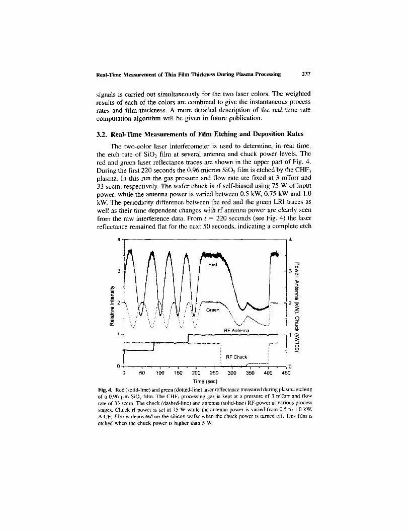
The two-color laser interferometer is used to determine, in real time,the etch rate of SiO2 film at several antenna and chuck power levels. Thered and green laser reflectance traces are shown in the upper part of Fig. 4.During the first 220 seconds the 0.96 micron SiO2 film is etched by the CHF3
plasma. In this run the gas pressure and flow rate are fixed at 3 mTorr and33 seem, respectively. The wafer chuck is rf self-biased using 75 W of inputpower, while the antenna power is varied between 0.5 kW, 0.75 kW and 1.0kW. The periodicity difference between the red and the green LRI traces aswell as their time dependent changes with rf antenna power are clearly seenfrom the raw interference data. From t = 220 seconds (see Fig. 4) the laserreflectance remained flat for the next 50 seconds, indicating a complete etch
Fig. 4. Red (solid-line) and green (dotted-line) laser reflectance measured during plasma etchingof a 0.96 n.m SiO2 film. The CHF3 processing gas is kept at a pressure of 3 mTorr and flowrate of 33 sccm. The chuck (dashed-line) and antenna (solid-line) RF-power at various processstages. Chuck rf power is set at 75 W while the antenna power is varied from 0.5 to 1.0 kW.A CFj film is deposited on the silicon wafer when the chuck power is turned off. This film isetched when the chuck power is higher than 5 W.
238 Sarfaty et al.
of the SiO2 film. At t = 270 seconds, the chuck power is turned off whilethe if antenna is kept at 1.0 kW. When the chuck power is turned off, a CFX
film starts to grow on the bare silicon wafer. This film is etched slowly when10 W of RF-power is applied to the wafer chuck and much more rapidly at75 W.
The instantaneous etch rates of SiO2, calculated for the first 220 secondsdata of the process described in Fig. 4, are shown in Fig. 5. The RF-powerapplied to the wafer chuck is 75 W and the corresponding rf antenna poweris plotted below the etch rates. The dashed and dotted lines represent thecalculated instantaneous etch rate using the green and the red lasers, respec-tively. The red laser trace, shown in Fig. 4, is noisier than the green laserwhich accounts for the difference seen in the estimated etch rate. The etchrate, shown in thick solid line, is the weighted combination of the separateetch rate results of the two lasers. Etch rate variations of 5-10% observedduring constant rf antenna power stage are typical to data with ~5% noise.Also, the initial slow rise time of the red laser etch estimation is due to theflat peak of the original red LRI trace, see Fig. 4, which is less sensitive toetch rate changes and is usually more noisy. The uncertainty in the final(thick line) etch rate calculation is half that of the red laser for this particularrun. The time response of the etch rate calculation is 5-10 seconds as seen
Fig. 5. Real-time etch rates of SiO2 film as a function of antenna rf power at a constant chuckpower of 75 W. The time dependent etch rates calculated with a single green (dashed-line) andred (dotted-line) laser reflectance and the combined rate (solid-line) are compared. The timeaveraged etch rates every half fringe for both colors are shown as solid points.
Fig. 6. Real-time thickness of the etched SiO2 film determined by the instantaneous etch ratesand the phase difference between the traces of the two-color laser reflectance. The time pointsof antenna rf-power changes are shown as vertical lines.
near the new set points of the antenna power. A faster response can beobtained but it introduces larger variations of the estimated etch rate for thecurrent quality of data points. The time response can be optimized to variousprocess rates by improving signal-to-noise ratio and varying the data samplingrate. The dark data points shown in Fig. 5 are the time averaged etch ratesdetermined every half fringe of film etching for both laser colors. The ratevariations between the two colors and from the instantaneous values aremainly due to peak detection uncertainties.
The instantaneous thickness of the etched SiO2 film, calculated in real-time, is given in Fig. 6 for the same first 220 seconds of data of the processdescribed in Fig. 4. The film thickness is derived from the phase differencebetween the LRI traces of the red and green lasers and the instantaneousetch rates given in Fig. 5. The changes in rf-power to the antenna are shownas vertical lines.
The two-color laser interferometer can be used, in real-time, to evaluateprocess rates as a function of any desired tool variable. In Fig. 7 the real-time etch rate of SiO2 is determined for a time varying wafer-chuck power.The red and green LRI data are the periodically varying traces shown in Fig.7 while the chuck power is the linear ramp rising from 0 W to 120 W. Duringthe first 60 seconds, the small initial fringe in Fig. 7 corresponds to a CFX
film that is deposited on top of the original SiO2 film at chuck power below
Real-Time Measurement of Thin Film Thickness During Plasma Processing 239
5 W and is etched at higher chuck power. Film deposition is represented bynegative etch rate and etching by positive values. At t = 60 seconds thereflected intensity reaches the initial value, which is the beginning of theetching of the SiO2 film. The dependence of SiO2 etch rate on chuck poweris determined, in real-time, in one continuous run using a single wafer.Similarly the rf power to the antenna, the gas flow rate and pressure, gasadditives, etc. were varied during the process, and the etch or growth rateof the associated film was calculated in real-time. This procedure simplifiesand considerably reduces the time required to develop, characterize, andoptimize a process.
A typical process of CFX film deposition is shown in Fig. 8 for fixedtool conditions. The antenna power is set at 1.0 kW and no rf power isapplied to the wafer chuck. The CHF3 gas flow is fixed at 40 seem and thepressure at 4 m Torn The instantaneous deposition rate of the CFX film variesin the range of 1.8-2.0 nm/s and is etched at a rate of —16 nm/s when aconstant 75 W of RF-power is applied to the wafer chuck. The values forthe refractive index and extinction coefficient of the CFX film at a wavelengthof 633 nm are 1.402 and 0.00447, respectively. These values were measuredby an ex situ multi-wavelength ellipsometer.
Fig. 7. Real-time calculated etch rates of SiO2 film (thick solid-line) for a linearly rising chuckpower from 0-120 W and a fixed antenna power of 750 W. The CHF3 processing gas is setat a pressure of 4 m Torr and flow rate of 30 seem. Also shown are the red (solid-line) andgreen (dotted-line) laser interference measured during the process characterization run.
240 Sarfaty et al.
Real-Time Measurement of Thin Film Thickness During Plasma Processing 241
Fig. 8. Real-time process rates (thick solid-line) calculated during deposition and etching ofCF, film using CHF, at a pressure of 4 mTorr and flow rate of 40 seem. The antenna poweris constant at 750 W; the chuck power is set to zero during film deposition (f < 735 sec.),and 75 W during film etching (f > 735 sec.). The red (solid-line) and green (dotted-line) laserreflectance traces measured during the process are shown.
The reflectance of both of the lasers decrease during the relatively long(720 seconds) deposition time, and maintained at the same peak intensityduring the relatively fast etching phase (100 seconds). The decrease of thelight intensity with time may result from film absorption, however, thereflected intensity does not reach the initial value after the film is completelyetched. Moreover, film absorption will manifest in LRI traces as a shrinkingenvelope similar to wave damping traces of oscillating waveforms. Also, themeasured low extinction coefficient of the CF, film can not explain theobserved decrease of the LRI traces. Therefore, it is more likely that laserscattering due to roughening of the film's surface(13) or of the quartz window,as well as coating of the window during the relatively long time scales, isthe reason for the observed drop in the LRI intensity during film deposition.A comparison similar to the study made in Ref. 13, between surface roughnessmeasured by atomic force microscopy and LRI traces, is required to determinethe reason for this behavior. However, the instantaneous deposition rates canstill be derived from these traces by re-scaling the measured LRI envelopeto the peak-normalized model traces. The computer program detects andupdates in real-time, the peaks of the measured LRI traces and re-scales themprior to the comparison with the model traces. The re-scaling of the measured
LRI is very important to avoid errors in the calculated etch or growth ratesof the film. Without proper peak scaling the phase information of the measuredLRI traces is misinterpreted and the comparison to the normalized modelwill be incorrect.
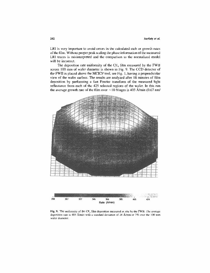
The deposition rate uniformity of the CFX film measured by the FWIIacross 100 mm of wafer diameter is shown in Fig. 9. The CCD detector ofthe FWII is placed above the MCICP tool, see Fig. 1, having a perpendicularview of the wafer surface. The results are analyzed after 18 minutes of filmdeposition by performing a fast Fourier transform of the measured lightreflectance from each of the 425 selected regions of the wafer. In this runthe average growth rate of the film over ~ 10 fringes is 403 A/min (0.67 nm/
Fig. 9. The uniformity of the CFX film deposition measured in situ by the FWII. The averagedeposition rate is 403 A/min with a standard deviation of 28 A/min or 7% over the 100 mmwafer diameter.
242 Sarfaty et at.
s) with a standard deviation of 7%. Similar instantaneous deposition rates inthe range of 0.6—0.7 nm/s were determined with the two-color laser interfer-ometer. The thickness of the deposited film (730 nm) determined by theFWII and the two-color laser interferometer was verified by the ex situmultiwavelength ellipsometry.
4. CONCLUSIONS
An in situ single point two-color laser interferometer is used to monitor,in real time, the thickness of thin transparent films during plasma processing.The rate of change of film thickness is determined instantaneously by compar-ing the measured and modeled laser reflectance interference from the filmand the substrate. The use of two different laser wavelengths provides higheraccuracy of the calculated rates and a clear distinction between film etchingand deposition. The film thickness is uniquely determined from the phasedifference in the reflected laser intensity between the two laser colors andthe measured etch rates. The local rate information is complemented by anin situ FWII, which uses a single wavelength of the plasma light emissionto determine the uniformity of the average process rates across the substrate.The post-process analysis of the FWII data requires a couple of fringes todetermine the average process rates, which may not be available for thinfilms of less than a single fringe. Also, the relatively fast response of thetwo-color laser interferometer to changes in the process rates makes it adesirable sensor for real-time process characterization and control. The combi-nation of both sensors provides real-time instantaneous local informationof film thickness, etch or growth rates, and global average uniformity ofthe process.
ACKNOWLEDGMENTS
The authors would like to thank P. Sandstrom for the construction ofthe electronic circuits used for computer control of the MCICP tool and fordata acquisition. We thank R. Parker for his technical assistance with theMCICP tool and the optical setup. This work was supported by the NationalScience Foundation under Grant No. EEC-8721545.
REFERENCES
1. H. H. Busta, Proc. Soc. Photo-opt. Intrum. Eng. 276. 164 (1981).2. P. J. Marcoux and P. D. Foo), Proc. Soc. Photo-opt. Intrum. Eng. 276, 170 (1981).3. M. Sternheim, W. Van Gelder. and A. W. Hartman. J. Electmchem. Soc. 130, 66 (1983).
Real-Time Measurement of Thin Film Thickness During Plasma Processing 243
4. G. Bruno. P. Capezzuto, G. Cicala, and F. Cramarossa, Plasma. Chem. and Plasma Process.6, 109 (1986).
5. B. R. Stoner, B. E. Williams, S. D. Walter, K. Niskimura, and J. T. Glass. J. Mater. Res.7, 257 (1995).
6. V. M. Donnely, D. L. Flamm, W. C. Dautremont-Smith. and D. ]. Werder, J. Appl. Phys.55, 242 (1984).
7. T. L. Vincent, P. P. Khargonekar, and F. L. Terry, Diagnostic Techniques for SemiconductorMaterial Processing II, S. W. Pang et al. (eds). Material Research Society. 87 (1996).
8. T. L. Vincent, P. P. Khargonekar, and F. L. Terry. IEEE Trans. Semiconductor Manufacturing,10(1997).
9. I. Tepermeister. W. T. Conner. T. Alzaben, H. Barnard, K. Gehlert. and D. Scipione, SolidState Technol. p. 63 (1996).
10. C. Lai. B. Brumnmeir. and R. C. Woods. J. Vac. Sci. Technol. A13, 2086 (1995).11. O. S. Heavens. Optical Properties of Thin Solid Films. Dover Publications. New York
(1991) . Republication of original text London: Butterworths Scientific Publications (1955).12. P. A. Heimann and R. J. Schutz, J. Electrochem. Soc. 131. 881 (1984).13. C. D. Zuiker. D. M. Greun, and A. R. Krauss, MRS Bull. XX, 29 (1995).


![Meyer-Neldel Rule in plasma Polythiophene thin filmsganic films formed by plasma, particularly in thin polymeric films . Pinto [8]explained the semiconductor [7] Pinto [8]explained](https://static.documents.pub/doc/80x56/5fe24fc5db0b443c095d66bb/meyer-neldel-rule-in-plasma-polythiophene-thin-films-ganic-films-formed-by-plasma.jpg)


